US8144528B2 - Memory with data control - Google Patents
Memory with data controlDownload PDFInfo
- Publication number
- US8144528B2 US8144528B2US12/699,627US69962710AUS8144528B2US 8144528 B2US8144528 B2US 8144528B2US 69962710 AUS69962710 AUS 69962710AUS 8144528 B2US8144528 B2US 8144528B2
- Authority
- US
- United States
- Prior art keywords
- packet
- command
- data
- input
- strobe signal
- Prior art date
- Legal status (The legal status is an assumption and is not a legal conclusion. Google has not performed a legal analysis and makes no representation as to the accuracy of the status listed.)
- Active, expires
Links
Images


Classifications
- G—PHYSICS
- G11—INFORMATION STORAGE
- G11C—STATIC STORES
- G11C7/00—Arrangements for writing information into, or reading information out from, a digital store
- G11C7/10—Input/output [I/O] data interface arrangements, e.g. I/O data control circuits, I/O data buffers
- G11C7/1078—Data input circuits, e.g. write amplifiers, data input buffers, data input registers, data input level conversion circuits
- G—PHYSICS
- G11—INFORMATION STORAGE
- G11C—STATIC STORES
- G11C7/00—Arrangements for writing information into, or reading information out from, a digital store
- G11C7/10—Input/output [I/O] data interface arrangements, e.g. I/O data control circuits, I/O data buffers
- G—PHYSICS
- G11—INFORMATION STORAGE
- G11C—STATIC STORES
- G11C7/00—Arrangements for writing information into, or reading information out from, a digital store
- G11C7/10—Input/output [I/O] data interface arrangements, e.g. I/O data control circuits, I/O data buffers
- G11C7/1078—Data input circuits, e.g. write amplifiers, data input buffers, data input registers, data input level conversion circuits
- G11C7/109—Control signal input circuits
- G—PHYSICS
- G11—INFORMATION STORAGE
- G11C—STATIC STORES
- G11C7/00—Arrangements for writing information into, or reading information out from, a digital store
- G11C7/22—Read-write [R-W] timing or clocking circuits; Read-write [R-W] control signal generators or management
- G—PHYSICS
- G11—INFORMATION STORAGE
- G11C—STATIC STORES
- G11C16/00—Erasable programmable read-only memories
- G11C16/02—Erasable programmable read-only memories electrically programmable
- G11C16/06—Auxiliary circuits, e.g. for writing into memory
- G11C16/10—Programming or data input circuits
- G11C16/102—External programming circuits, e.g. EPROM programmers; In-circuit programming or reprogramming; EPROM emulators
- G—PHYSICS
- G11—INFORMATION STORAGE
- G11C—STATIC STORES
- G11C2207/00—Indexing scheme relating to arrangements for writing information into, or reading information out from, a digital store
- G11C2207/10—Aspects relating to interfaces of memory device to external buses
- G11C2207/107—Serial-parallel conversion of data or prefetch
- G—PHYSICS
- G11—INFORMATION STORAGE
- G11C—STATIC STORES
- G11C2216/00—Indexing scheme relating to G11C16/00 and subgroups, for features not directly covered by these groups
- G11C2216/12—Reading and writing aspects of erasable programmable read-only memories
- G11C2216/30—Reduction of number of input/output pins by using a serial interface to transmit or receive addresses or data, i.e. serial access memory
Definitions
- memory systemsoften comprise a controller and one or more memory devices.
- the controllertypically contains circuitry configured to generate signals that are used to direct the memory devices to store and retrieve information.
- the memory devicestypically store the information in memory that is contained in the memory devices.
- the memorymay be volatile or non-volatile.
- a memory device that contains volatile memoryoften loses the stored information when power is removed from the device.
- a memory device containing non-volatile memoryoften retains the stored information even when power is removed from the device.
- data and control signalsare transferred between the controller and memory devices in parallel using a parallel bus.
- a parallel busoften, many wires are used to implement the bus and, depending on the layout of the memory system, the wires may extend for some length.
- FIG. 1is a block diagram of an example of a memory system that may be used with an embodiment of the invention
- FIG. 2is a block diagram of an example of a memory device that may implement an embodiment of the invention
- FIG. 3is a flow chart of a sequence of steps that may be used to input a command packet into a memory device in accordance with an embodiment of the invention
- FIG. 4is a timing diagram that illustrates timing information that may be used to input a command packet into a memory device in accordance with an embodiment of the invention
- FIG. 5is a flow chart of a sequence of steps that may be used to input a write data packet into a memory device in accordance with an embodiment of the invention
- FIG. 6is a timing diagram that illustrates timing information that may be used to input a write data packet into a memory device in accordance with an embodiment of the invention
- FIG. 7is a flow chart of a sequence of steps that may be used to output a read data packet from a memory device in accordance with an embodiment of the invention.
- FIG. 8is a timing diagram that illustrates timing information that may be used to output a read data packet from a memory device in accordance with an embodiment of the invention
- FIGS. 9A-Bare a flow chart of a sequence of steps that may be used to store data in a memory device in accordance with an embodiment of the invention.
- FIG. 10is a timing diagram that illustrates timing information that may be used to store data in a memory device in accordance with an embodiment of the invention.
- FIGS. 11A-Bare a flow chart of a sequence of steps that may be used to retrieve data from a memory device in accordance with an embodiment of the invention.
- FIG. 12is a timing diagram that illustrates timing information that may be used to retrieve data from a memory device in accordance with an embodiment of the invention
- FIGS. 13A-Bare a flow chart of a sequence of steps that may be used to pause and resume the inputting of a write data packet into a memory device in accordance with an embodiment of the invention.
- FIG. 14is a timing diagram that illustrates timing information that may be used to pause and resume the inputting of a write data packet into a memory device in accordance with an embodiment of the invention.
- commandsare used to direct the memory devices to perform various operations (e.g., read data, write data).
- the commandsare typically embedded in a serial data stream that is transferred from a controller to the memory devices via a serial bus.
- Parameters that are associated with the commande.g., addresses, data
- the command and parameter informationmay be “tagged” with codes so that they may be identified by the memory devices. For example, a two-bit code may precede a command in the serial stream to indicate that the information following the code is a command. Likewise, data and address information may each be preceded in the stream with codes to identify this information.
- serial bus designOne problem with the above-described serial bus design is that the codes in the serial bit stream tend to add a significant amount of overhead to the command and parameter information carried in the stream. For example, if a two-bit code is used to identify a 4-bit command, the overhead added by the code is fifty percent. Moreover, adding the codes to the bit stream may impact performance and consume valuable space in the bit stream that may be otherwise used to carry other information, such as additional commands and their associated parameters as well as additional data.
- a memory devicecomprises memory, a first data link, a first input, a second input, a second data link, a first output and a second output.
- the first data linkis configured to input one or more packets into the memory device.
- a packetrelates to a sequence of data (e.g., bytes of data) that may be formatted to contain various information, such as commands, parameters, data and so on.
- the first inputis configured to input a command strobe signal into the memory device.
- the command strobe signaldelineates a command packet (i.e., indicates the start and end of the packet) that is input into the memory device at the first data link.
- a command packetis illustratively a packet that contains a command that may be executed by the memory device.
- the command packetmay also contain various parameter information associated with the command, such as address information.
- the second inputis configured to input a data strobe signal into the memory device.
- the data strobe signaldelineates a write data packet that is input into the memory device at the first data link.
- a write data packetis illustratively a packet that contains data that may be stored in the device's memory.
- the second data linkis configured to output information, such as packets and status, from the memory device. Packets that are output from the device may include command packets that are bypassed by the device and read data packets.
- a read data packetis illustratively a packet that contains data that may have been read from the device's memory.
- the first outputis configured to output a command strobe signal that is bypassed by the memory device.
- the second outputis configured to output a data strobe signal that is bypassed by the memory device.
- Bypassed command packetsare illustratively output from the device simultaneously with bypassed command strobe signals which delineate the command packets.
- read data packetsare illustratively output from the memory device simultaneously with bypassed data strobe signals which delineate the read data packets.
- FIG. 1is a block diagram of an example of a memory system that may be used with an embodiment of the invention.
- System 100comprises a controller 110 connected to a memory device 200 via a series of electrical connections.
- the controller 110comprises circuitry configured to generate various control signals and packets that are used to store data in the memory device 200 and retrieve stored data from the device 200 .
- the control signals and packetsare transferred between the memory device 200 and the controller 110 via the electrical connections.
- the packetsmay include command packets that contain commands and associated parameters that are used, for example, to direct the memory device 200 to store data into and retrieve data from memory contained in the device 200 .
- the packetsmay include write data packets that contain data that are to be stored in the memory and read data packets that contain data that have been retrieved from the memory.
- NAND flash memoryNOR flash memory
- AND flash memoryserial flash memory
- Divided Bit-line NOR (DiNOR) flash memoryDynamic Random Access Memory (DRAM), Synchronous RAM (SRAM), Ferro-electric RAM (FRAM), Magnetic RAM (MRAM), Phase Change RAM (PCRAM), Read Only Memory (ROM), Electrically Erasable Programmable ROM (EEPROM) and so on.
- DRAMDynamic Random Access Memory
- SRAMSynchronous RAM
- FRAMFerro-electric RAM
- MRAMMagnetic RAM
- PCRAMPhase Change RAM
- ROMRead Only Memory
- EEPROMElectrically Erasable Programmable ROM
- FIG. 2is a block diagram of an example of a memory device 200 that may implement an embodiment of the invention.
- Memory device 200comprises various circuitry including circuitry configured to store and retrieve data in response to commands that are input into the device 200 . More specifically, memory device 200 comprises an internal voltage generator 260 , a row/column pre-decoder and array control 230 , row decoders 210 , page buffer 217 , memory 205 , column decoders 220 , data control unit and registers 225 , configuration register 235 , command and address processing unit 240 , input and output data processing unit 245 , control interface 250 and input and output buffers 255 .
- the internal voltage generator 260comprises circuitry configured to generate various voltage levels used by various circuitry contained in the memory device 200 .
- the row/column pre-decoders and array control 230comprise circuitry configured to pre-decode row address and column address information that is transferred from the command and address processing unit 240 .
- the row decoders 210comprise circuitry configured to perform final decoding of row address information provided by the row/column pre-decoders 230 .
- the final decoded row address informationis used to select a location in memory 205 were data is to be stored or retrieved.
- the column decoders 220comprise circuitry configured to perform final decoding of column address information provided by the row/column pre-decoders 230 .
- the final decoded column address informationis used to select a specific column in the page buffer 217 .
- the data control unit and registers 225comprise circuitry configured to process and store information that is transferred to and from the page buffer 217 .
- the page buffer 217is a data buffer that comprises circuitry configured to temporarily hold (1) write data that is to be stored into memory 205 and (2) read data that is retrieved from memory 205 .
- Memory 205comprises circuitry configured to implement a data storage that may be used to store data.
- Memory 205may include one or more memory banks that are used to store the data.
- the memory 205may be volatile or non-volatile.
- Datais illustratively stored (written) into and retrieved (read) from memory 205 on a per page basis.
- a pageis 2112 bytes in length. It should be noted that other page sizes are used in other embodiments of the invention. It should be also noted that in other embodiments of the invention, data is stored and retrieved from memory on a non-page basis.
- the configuration register 235comprises circuitry configured to store various configurable (programmable) and/or read-only configuration information associated with the device 200 .
- This informationillustratively includes a device address that is associated with the memory device 200 and link-width information that specifies a width of the device's Dn input data link and the device's Qn output data link.
- the link width informationspecifies the number of bits of information that may be simultaneously clocked into the device 200 at the Dn input or clocked out of the device 200 at the Qn output. For example, if the specified link width is one bit, then one bit of information may be clocked into the Dn input or clocked out of the Qn output at a time. Likewise, for example, if the specified link width is eight bits, then eight bits of information may be clocked into the Dn input or clocked out of the Qn output at a time.
- the command and address processing unit 240comprises circuitry configured to process commands contained in command packets that are input into the device 200 .
- This processingillustratively includes executing the commands and processing (e.g., decoding) row and column address information from address information that may be contained in the command packets.
- the processed row and column informationis transferred by the command and address processing unit 240 to the row/column pre-decoders and array control 230 to, inter alia, select various locations in memory 205 where data is stored and retrieved.
- the input and output data processing unit 245comprises circuitry configured to process data transferred to and from the device 200 . This processing illustratively includes serializing and de-serializing the data.
- Control interface 250comprises circuitry configured to implement various inputs and outputs of the device 200 .
- the inputsinclude an RST# input, CE# input, CK input, CK# input, CSI input and DSI input.
- the outputsinclude a CSO output, a DSO output, an optional CKO output and an optional CKO# output.
- Signals that may be input into the device 200include a reset signal, a chip enable signal, a clock input signal and its inverse, a command strobe signal and a data strobe signal which are input into the device 200 via the device's RST#, CE#, CK, CK#, CSI and DSI inputs, respectively.
- Signals that may be output from the device 200include a clock output signal and its inverse, a command strobe signal and a data strobe signal which are output from the device 200 via the device's CKO, CKO#, CSO, and DSO outputs, respectively.
- the reset signalmay be used to reset the device 200 .
- Inputting an activated reset signal (e.g., setting the signal to a logical low state) into the device 200 at the device's RST# inputcauses the device 200 to reset.
- the chip enable signalmay be used to enable the device 200 .
- Inputting an activated chip enable signal into the device 200 at the device's CE# inputcauses the device 200 to be enabled (operative). Enabling a device 200 activates internal clock signals in the device 200 and makes the device 200 capable of accepting and processing commands.
- Inputting a deactivated chip enable signal into the device 200 at the device's CE# inputdisables the device 200 , deactivates the device's internal clock signals and makes the device 200 inoperative (e.g., incapable of accepting and processing commands).
- the clock input signal and its inverseare external system clock signals that may be used to provide an external clock to the device 200 .
- the clock input signal and its inverseare differential clock signals meaning that one is the complement of the other.
- Command and data packetsmay be synchronously input into or output from the device 200 using the clock input signal or its inverse.
- statusmay be synchronously output from the device using the clock input signal or its inverse.
- the clock output signal and its inverseare copies of the clock input signal and its inverse, respectively.
- a command strobe signal that is inputted into a device 200may be used to delineate a command packet that is inputted into the device 200 at the device's Dn input.
- a command strobe signal that is outputted from a device 200is a copy of a command strobe signal that is inputted into the device 200 .
- a command strobe signal that is outputted from a device 200may be used to delineate a command packet that is output (bypassed) by the device 200 at the device's Qn output.
- a data strobe signal that is inputted into a device 200may be used to delineate a write data packet that is inputted into the device 200 at the device's Dn input.
- a data strobe signal that is outputted from a device 200is a copy of a data strobe signal that is inputted into the device 200 .
- a data strobe signal that is outputted from a device 200may be used to delineate a read data packet that is output from the device 200 at the device's Qn output.
- a data strobe signal that is outputted from a device 200may be used to indicate status is output from the device 200 at the device's Qn output.
- the Dn inputis a data link that is used to input packets (e.g., write data packets, command packets) into the device 200 .
- a packetis illustratively input into the device 200 at the Dn input by clocking a portion of the packet into the device 200 at a transition of the clock input signal or its inverse.
- the size of the portion that is clocked into the device 200 at a timedepends on the width of the data link as specified in the configuration register 235 . For example, if the data link is specified as being one bit wide, then the size of the portion is one bit and one bit of the packet is clocked into the device 200 at a time. Likewise, for example, if the data link width is eight bits wide, then the size of the portion is eight bits and eight bits of the packet are clocked into the device at a time.
- the transition of the clock signal that is used to clock the portion of the packet into the device 200depends on the data rate arrangement used for the device 200 .
- a portion of the packetmay be clocked into the device 200 at each upward or downward transition of CK or CK#.
- DDRdouble data rate
- a portion of the packetmay be clocked into device 200 at each upward and downward transition of CK or CK#.
- QDRquad data rate
- ODRocta data rate
- the Qn outputis a data link that is used to output information (e.g., bypassed command packets, read data packets, status) from the memory device 200 .
- the amount of information that is output from the device 200 at a timedepends on the width of the data link. Thus, for example, if the data link is one bit wide then a single bit of information is output from the device 200 at a time. Likewise, if the width of the data link is multiple bits wide, then multiple bits of information are output from the device 200 at a time.
- Informationis illustratively output from the device 200 at the Qn output by clocking a portion of the information out of the device 200 at a transition of the clock input signal or its inverse.
- the amount of information that is clocked out of the device 200 at a timedepends on the width of the data link as specified in the configuration register 235 . For example, if the data link is one bit wide, then one bit of information is clocked out of the device 200 at a time. Likewise, for example, if the data link width is eight bits wide, then eight bits of information are clocked out of the device 200 at a time.
- the transition of the clock signal that is used to clock the information out of the device 200depends on the data rate arrangement used for the device 200 .
- a portion of the informationmay be clocked out of the device 200 at each upward or downward transition of CK or CK#.
- a portion of the informationmay be clocked out of the device 200 at each upward and downward transition of CK or CK#.
- other data rate arrangementsmay be used to clock information out of the device 200 including a QDR arrangement, an ODR arrangement and so on.
- the CSI, DSI and Dn inputs and, the CSO, DSO and Qn outputs togethercomprise a serial link interface for device 200 .
- the device 200may contain one or more serial link interfaces and the serial link interfaces may operate independently of each other.
- control interface 250receives an activated command strobe signal at the device's CSI input, generates an internal command strobe signal (int_CSI), from the activated command strobe signal and transfers the internal command strobe signal to the input and output buffers 255 to condition the buffers 255 to receive (clock in) a command packet at the device's Dn input.
- the input and output buffers 255clock the command packet into the device 200 and transfer the command packet to the command and address processing unit 240 via an internal serial “data in” (sdin) bus.
- the command and address processing unit 240processes the command packet including parsing address information that may be contained in the packet and executing a command contained in the packet.
- the command and processing unit 240transfers the parsed address information to the row/column pre-decoders and array control 230 . If the parsed address information contains a row address, the row/column pre-decoders and array control 230 transfers the row address to the row decoders 210 which select a page in memory 205 associated with the row address. If the parsed address information contains a column address, the row/column pre-decoders and array control 230 transfers the column address to the column decoders 220 which select a starting column in the page buffer 217 associated with the column address.
- the command and address processing unit 240places the device 200 in a write mode by generating a write signal and transferring the write signal to the input and output data processing unit 245 to direct the unit 245 to receive a write data packet containing write data that is to be written into memory 205 .
- the command and address processing unit 240transfers the column address contained in the command packet to the row/column pre-decoders and array control 230 to select a starting column in the page buffer 217 where the write data is to be written.
- a data strobe signal that is received at the device's DSI inputis converted into an internal data strobe signal (int_DSI) by the control interface 250 .
- the control interface 250then transfers the internal data strobe signal to the input and output buffers 255 to direct the buffers 255 to receive the write data packet.
- the input and output buffers 255receive (clock in) the write data packet at the device's Dn input and transfer the write data packet to the input and output data processing unit 245 via the sdin bus.
- the input and output data processing unit 245de-serializes the write data packet and transfers the write data contained therein to the data control unit and registers 225 .
- the data control unit and registers 225transfer the write data to the page buffer 217 starting at the column address selected by the column decoders 220 .
- a command packet containing a page program command and a row address that is later received by the device 200is transferred to the command and address processing unit 240 which (1) executes the page program command, (2) transfers the row address to the row/column pre-decoders and array control 230 to select a page in memory 205 where the write data is to be written and (3) directs the data control unit and registers 225 to write the write data contained in the page buffer 217 into the selected page in memory 205 .
- a command packet, received by the device 200contains a page read command
- the command and address processing unit 240generates a read signal and transfers the read signal to the input and output data processing unit 245 .
- the command and address processing unit 240transfers a row address contained in the command packet to the row/column pre-decoders and array control 230 to select a row in memory where the read data is stored.
- the read data at the selected rowis read from memory 205 and placed in the page buffer 217 .
- the input and output data processing unit 245serializes the read data and transfers the serialized read data to the input and output buffers 255 via an internal serial “data out” (sdout) bus.
- a command packet containing a burst data read command and a column address that is later received by the device 200is transferred to the command and address processing unit 240 which (1) executes the burst data read command and (2) places the device 200 in a read mode by generating a read signal and transferring the read signal to the input and output data processing unit 245 to direct the unit 245 to output the read data to the input and output buffers 255 .
- the input and output data processing unit 245receives the read signal, serializes the read data and transfers the serialized read data to the input and output buffers 255 .
- a data strobe signal received at the device's DSI inputis converted into an internal data strobe signal (int_DSI) by the control interface 250 .
- the control interface 250transfers the internal data strobe signal to the input and output buffers 255 to direct the buffers 255 to output the serialized read data.
- the input and output buffers 255output (clock out) the serialized read data from the device 200 at the device's Qn output.
- Table 1illustrates an example of information that may be contained in a command packet that is input into a device 200 .
- the device addressis used to a address command packet to one or more devices 200 in a system.
- the device addressmay be a unicast address that is used to address the command packet to a particular device 200 .
- the addressmay be a multicast address that is used to address the command packet to one or more devices 200 that belong to a particular multicast group.
- a device 200 that receives a command packet that is (1) addressed to the device 200 or (2) addressed to a multicast group to which the device 200 belongsperforms (executes) the command contained in the command packet.
- the device addressmay be omitted.
- the device addressmay be necessary in order to identify those devices 200 in the system that are to perform the command.
- the commandis used to direct the device 200 to perform a particular operation.
- a page read commandmay be used to direct the device 200 to read a page of data from the device's memory 205 and place the data in the device's page buffer 217 .
- a burst data read commandmay be used to direct the device 200 to output data contained in the device's page buffer 217 from the device 200 at the device's Qn output.
- a commandis represented in a command packet by an operation (OP) code.
- the row addressis used to specify a starting memory location contained in memory 205 where the command is to be performed. For example, for a page read command, the row address specifies a starting address of a page in memory 205 where data is read.
- the column addressspecifies a starting address of a column in the page buffer 217 where the operation is performed. For example, for a burst data read command, the column address specifies a starting column in the page buffer 217 where data is read.
- Table 2illustrates example formats that may be used to format a command packet that is input into a device 200 .
- a command packet that may be used to direct a device 200 to perform a page read operationmay contain a one-byte device address (DA) associated with the device 200 , followed by a one-byte OP code (i.e., 00h) that indicates a page read command and followed by a three-byte row address (RA) which specifies a row address associated with the command.
- DAdevice address
- RAthree-byte row address
- a command packet that may be used to direct a device 200 to perform a burst data read operationmay contain a one-byte device address associated with the device 200 , followed by a one-byte OP code (i.e., 20h) that indicates a burst data read command and followed by a two-byte column address (CA) which specifies a column address associated with the command.
- a one-byte OP codei.e., 20h
- CAtwo-byte column address
- FIG. 3is a flow chart of a sequence of steps that may be used to input a command packet into the memory device 200 in system 100 in accordance with an embodiment of the invention.
- the sequencebegins at step 305 and proceeds to step 310 where the controller 110 outputs (1) an activated command strobe signal at the controller's CSO output and (2) a first portion of the command packet at the controller's Qn output.
- the memory device 200receives the command strobe signal at its CSI input and inputs (clocks) the first portion of the command packet into the device 200 at its Dn input, as described above.
- the controller 110determines if the last portion of the command packet has been outputted from the memory controller 110 . If not, the sequence proceeds to step 340 where the controller 110 outputs the next portion of the command packet and the memory device inputs 200 the next portion into the device 200 , as described above.
- step 330the controller 110 determines that the last portion of the command packet has been outputted from the controller 110 , the sequence proceeds to step 350 where the controller outputs a deactivated command strobe signal at its CSO output to indicate the end of the command packet.
- step 360the memory device 200 receives the deactivated command strobe signal at its CSI input and concludes the entire command packet has been input into the device 200 . The sequence ends at step 395 .
- FIG. 4is a timing diagram that illustrates timing information that may be used to input a command packet into a memory device 200 in accordance with an embodiment of the invention.
- the command packetcontains device address (DA), command (CMD) and address (ADDR) information.
- An activated command strobe signalis input into the memory device 200 at the device's CSI input. While the command strobe signal is activated, a portion of the command packet present at the device's Dn input is clocked into the device 200 at a clock edge associated with the clock signal that is present at the CK or CK# inputs. Subsequent portions of the command packet are clocked into the device 200 at subsequent clock transitions.
- the number of bits of the command packet that comprise the portiondepends on the width of Dn specified in the configuration register 235 .
- Time t ISrepresents an input setup time and time t IH represents an input hold time for the portion of the command packet that is presented at the Dn input.
- the command strobe signalis activated for the duration of the command packet and is used to delineate the command packet.
- the command strobe signalis deactivated after the last portion of the command packet has been clocked into the device 200 .
- the device 200bypasses the command strobe signal by outputting a copy of the command strobe signal at the device's CSO output at a time t IOL (input/output latency time) which is a latency time from the time the command strobe signal was input into the device 200 .
- a time t IOLinput/output latency time
- device 200bypasses the command packet by clocking the command packet out of the device 200 portion-by-portion, as described above, at the device's Qn output at each edge of a clock signal that is present at the CK or CK# inputs.
- the number of bits that comprise the portiondepends on the width of Qn specified in the configuration register 235 , as described above.
- the time t OHrepresents a hold time where the information outputted at the Qn output is valid.
- the time t OArepresents an output access time.
- a command packetis some multiple of bytes in length and each byte may be input into the device 200 using four clock cycles.
- the activated command strobe signalis present at the device's CSI input and CSO output for some multiple of four clock cycles for each command packet depending on the length of the command packet. If, for example, the command packet is five bytes in length, the activated command strobe signal is present at the device's CSI input and CSO output for twenty clock cycles each.
- FIG. 5is a flow chart of a sequence of steps that may be used to input a write data packet into the memory device 200 in system 100 in accordance with an embodiment of the invention.
- the sequencebegins at step 505 and proceeds to step 510 where the controller 110 outputs an activated data strobe signal at the controller's DSO output and outputs a first portion of the write data packet at the controller's Qn output.
- the memory device 200receives the activated data strobe signal at the device's DSI input and inputs the first portion of the write data packet into the device 200 at the device's Dn input, as described above.
- the controller 110determines if the last portion of the write data packet has been outputted from the memory controller 110 . If not, the sequence proceeds to step 540 where the controller 110 outputs the next portion of the write data packet and the memory device 200 inputs the next portion into the device 200 , as described above.
- step 530the controller 110 determines that the last portion of the write data packet has been outputted from the memory controller 110 , the sequence proceeds to step 550 where the controller outputs a deactivated data strobe signal at the controller's DSO output to indicate the end of the write data packet.
- step 560the memory device 200 receives the deactivated data strobe signal at the device's DSI input and concludes the write data packet has been input into the device. The sequence ends at step 595 .
- FIG. 6is a timing diagram that illustrates timing information that may be used to input a write data packet into a memory device 200 in accordance with an embodiment of the invention. While the data strobe signal is activated at the device's DSI input, the portion of the data packet present at the device's Dn input is clocked into the device 200 at a clock edge associated with the clock signal present at the CK or CK# inputs. Subsequent portions of the write data packet are clocked into the device 200 at subsequent clock transitions. The number of bits of the write data packet that comprise the portion depends on the width of Dn, as noted above.
- Time t ISrepresents a setup time and time t IH represents a hold time for the portion of the write data packet that is presented at the Dn input.
- the data strobe signalis activated for the duration of the write data packet and is used to delineate the write data packet.
- the data strobe signalis deactivated after the last portion of the write data packet has been clocked into the memory device 200 .
- the write data packetis input into the memory device 200 while the device 200 is in a write mode.
- the memory device 200enters the write mode in response to executing a command (e.g., a burst data load start command, a burst data load command).
- the write modeis a mode where the memory device 200 is configured to (1) receive (input) a write data packet via the device's Dn input and (2) transfer write data contained in the write data packet to the page buffer 217 . While the device 200 is in the write mode, the DSO and Qn outputs are configured to maintain a steady state and not be affected by the state of the write data packet while it is input into the device 200 .
- the device 200exits the write mode by executing another command (e.g., a page program command) contained in another command packet that is later input into the device 200 .
- another commande.g., a page program command
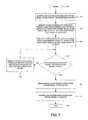
- FIG. 7is a flow chart of a sequence of steps that may be used to output a read data packet from the memory device 200 in system 100 in accordance with an embodiment of the invention.
- the sequencebegins at step 705 and proceeds to step 710 where the controller 110 requests the read data packet from the device by outputting an activated data strobe signal for the length of the read data packet at the controller's DSO output.
- the activated data strobe signaldelineates the requested read data packet.
- memory device 200receives the activated data strobe signal at the device's DSI input, outputs a copy of the activated data strobe signal at the device's DSO output and outputs a first portion of the data packet at the device's Qn output, as described above.
- the controller 110receives the copy of the activated data strobe signal from the device 200 at the controller's DSI input and clocks in the first portion of the read data packet at the controller's Dn input at a transition of a clock signal present at the controller's CK or CK# input.
- the memory device 200determines if a last portion of the read data packet has been outputted from the memory device 200 . If not, the sequence proceeds to step 750 where the memory device 200 outputs the next portion of the read data packet and the controller 110 inputs this next portion of the read data packet into the controller 110 , as described above. The sequence then returns to step 740 .
- step 740the memory device 200 determines that the last portion of the read data packet has been outputted by the memory device 200 .
- the sequenceproceeds to step 760 where the memory device 200 outputs a deactivated data strobe signal at its DSO output.
- step 770the controller 110 receives the deactivated data strobe signal at its DSI input and concludes the read data packet has been outputted from the device 200 . The sequence ends at step 795 .
- FIG. 8is a timing diagram that illustrates timing information that may be used to output a read data packet from a memory device 200 in accordance with an embodiment of the invention.
- a data strobe signalis activated and received by the device 200 at the device's DSI input, as described above.
- the time t ISrepresents a setup time for the activated data strobe signal and the time t IH represents a hold time for activated data strobe signal.
- the device 200outputs a copy of the activated data strobe signal at the device's DSO output.
- the outputted data strobe signalis activated for the same duration as the received activated data strobe signal.
- Time t OLis an output latency time that represents a time from when the activated data strobe signal was recognized by the device 200 to the time that a first portion of the read data packet is present at the device's Qn output. At each clock transition, a portion of the read data packet is presented at the device's Qn output.
- Time t OArepresents an output access time and time t OH represents an output hold time for the portion of the read data packet that is presented at the device's Qn output.
- the read data packetis output from the device 200 while the device 200 is in a read mode.
- the device 200enters the read mode by executing a command, such as a burst data read command, and exits the read mode when another command is input into the device 200 .
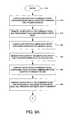
- FIGS. 9A-Bare a flow chart of a sequence of steps that may be used to store data in the memory device 200 in system 100 in accordance with an embodiment of an invention.
- the sequencebegins at step 905 and proceeds to step 910 where the controller 110 outputs a command packet containing a burst data load start command and a column address, as described above.
- the memory device 200inputs the command packet, as described above, and processes it including entering a write mode.
- the controller 110outputs a write data packet, containing data to be written into the device's memory 205 , to the memory device 200 , as described above.
- the memory device 200inputs the write data packet, at step 925 , as described above, and transfers write data contained in the write data packet to the device's page buffer 217 starting at the column address specified in the command packet.
- the controller 110outputs a command packet containing a page program command and a row address.
- the memory device 200inputs the command packet, as described above, and processes it including transferring the contents of the page buffer to memory 205 starting at the location specified by the row address contained in the command packet.
- the controller 110outputs a command packet, containing a read status register command, to the memory device 200 .
- the read status register commandmay be used to direct the device 200 to output a status of the device 200 .
- the memory device 200inputs the command packet, as described above, and processes it including entering a read mode.
- the controller 110requests the status from the device 200 by outputting an activated data strobe signal at its DSO output, as described above.
- the device 200receives the request (i.e., the activated data strobe signal) at its DSI input and outputs the requested status at its Qn output.
- the controller 110inputs the requested status at its Dn input.
- the controller 110determines if the status indicates that the memory device 200 is ready.
- the memory device 200outputs a status that indicates the device 200 is ready after it has completed writing the data to memory 205 . If the status does not indicate that the device 200 is ready, the sequence returns to step 955 . Otherwise, the sequence proceeds to step 970 where the controller 110 outputs a deactivated data strobe signal at its DSO output and concludes the data has been written into the device's memory 205 .
- the sequenceends at step 995 .
- FIG. 10is a timing diagram that illustrates timing information that may be used to store data into a memory device 200 in accordance with an embodiment of the invention.
- a command packetthat is addressed to the device 200 and contains a burst data load start command and a column address, is inputted into the device 200 , as described above.
- the column addressindicates a starting address in the device's page buffer 217 where the data is to be written. Since the command packet is addressed to the device 200 , the device 200 processes the command and enters a write mode which is designated in the timing diagram as time T 1 through T 2 .
- An activated data strobe signalis input into the device 200 at the device's DSI input at a time t CDS which is a CSI to DSI separation time and a write data packet, containing the data to be written into the device's memory 205 , is inputted into the device 200 at the device's Dn input, as described above.
- the data contained in the write data packetis placed in the device's page buffer 217 starting at the starting column address specified in the command packet.
- a command packetcontaining the device's device address, a page program command and a row address, is input into the device 200 , as described above.
- the command packetis inputted into the device 200 after a time interval t DCS which is a DSI to CSI separation time.
- the page program commanddirects the device 200 to write the data contained in the page buffer 217 into the device's memory 205 starting at the row address contained in the command packet.
- a command packet, containing a read status command,is then input into device 200 , as described above.
- the read status commandcauses the device 200 to enter a read mode (designated in the diagram as time T 3 through T 4 ) and output the status of the device 200 (e.g., busy, ready) at the device's Qn output.
- An activated data strobe signalis input into the device 200 at the device's DSI input, as described above, to request that the device 200 output the status.
- the data strobe signalis activated after a time t CDS which is a CSI to DSI separation time. While device 200 is busy writing the data into memory 205 , the device 200 reports a busy status at the device's Qn output.
- the device 200After the device 200 has finished writing the data into memory 205 , the device 200 reports a ready status at the device's Qn output. After the device reports a ready status, the data strobe signal that is input into the device's DSI input is deactivated. The next command that is inputted into the device 200 causes the device to exit the read mode.
- FIGS. 11A-Bare a flow chart of a sequence of steps that may be used to retrieve data from the memory device 200 in system 100 in accordance with an embodiment of the invention.
- the sequencebegins at step 1105 and proceeds to step 1110 where the controller 110 outputs a command packet containing a page read command and a row address.
- the memory device 200inputs the command packet, as described above, and processes it including retrieving data from memory 205 , starting at the row address contained in the command packet, and transferring the retrieved data to the device's page buffer 217 .
- the controller 110outputs a command packet containing a read status command.
- the memory device 200inputs the command packet, as described above, and processes it including entering a read mode.
- the controller 110requests the status of the device, as described above.
- the memory device 200receives the request and outputs the status at the device's Qn output, as described above.
- the controller 110inputs the status and examines it.
- the controller 110determines if the status indicates the device 200 is ready.
- the device 200indicates a ready status after it has completed the page read command. If the status does not indicate the device 200 is ready, the sequence returns to step 1135 ; otherwise, the sequence proceeds to step 1150 ( FIG. 11B ) where the controller 110 outputs a command packet containing a burst data read command and a column address.
- the memory device 200inputs the command packet containing the burst data read command and column address, as described above, and exits the read mode associated with the read status command.
- the memory device 200processes the command packet, containing the burst data read command and column address, including entering a read mode (associated with the burst data read command) and retrieving the data from the page buffer 217 starting at the column address specified in the command packet.
- the controller 110requests data from the memory device 200 by outputting an activated data strobe signal, as described above.
- the memory device 200receives the request and outputs a read data packet, containing the retrieved data, to the controller 110 , as described above.
- the controller 110receives the read data packet containing the retrieved data. The sequence ends at step 1195 .
- FIG. 12is a timing diagram that illustrates timing information that may be used to retrieve data from a memory device 200 in accordance with an embodiment of the invention.
- An activated command strobe signalis input into the device 200 at the device's CSI input and a command packet, containing a page read command and a row address, is input into the device 200 at the device's Dn input, as described above.
- the row addressis used to select a page in memory 205 that contains the data that is retrieved.
- the device 200processes the command packet including retrieving the data from memory 205 starting at a page indicated by the row address and transferring the data to the device's page buffer 217 .
- a command packet, containing a read status command,is then input into the device 200 , as described above.
- the device 200enters a read mode (illustrated in the timing diagram as the time T 1 to T 2 ) and outputs the status of the device 200 (e.g., busy, ready) at the device's Qn output, as described above. While the device 200 is busy reading data from memory 205 , the device 200 reports a busy status at the device's Qn output. Time t R indicates a time where data is being read from memory 205 and transferred to the device's page buffer 217 . After the device 200 has finished reading the data from memory 205 and transferring the data to the page buffer 217 , the device 200 reports a ready status at the device's Qn output.
- a command packet, containing a burst data read command and a column address,is then input into the device 200 , as described above. Note that the read mode associated with the read status command is exited at the time an activated CSI signal is input into the device 200 .
- the burst data read commandplaces the device 200 into a read mode, associated with the burst data read command, (illustrated in the diagram the time T 3 to T 4 ) and causes data contained in the page buffer 217 to be output from the device 200 .
- the column address contained in the command packetrepresents a starting address in the page buffer 217 where data is read.
- An activated data strobe signalis then received by the device 200 at the device's DSI input and, (1) the device 200 outputs the received activated data strobe signal at the device's DSO output and (2) outputs a read data packet, containing the data, at the device's Qn output, as described above.
- a successive command packet that is input into the device 200causes the device to exit the read mode associated with the burst data read command.
- FIGS. 13A-Bare a flow chart of a sequence of steps that may be used to pause and resume the inputting of a write data packet into the memory device 200 in system 100 in accordance with an embodiment of the invention.
- the sequencebegins at step 1305 and proceeds to step 1310 where the controller 110 outputs an activated data strobe signal at the controller's DSO output and outputs a first portion of the write data packet to the memory device 200 , as described above.
- the memory device 200receives the activated data strobe signal at its DSI input and inputs the first portion of the data packet into the device 200 , as described above.
- the controller 110determines if a last portion of the data packet has been outputted from the controller 110 . If so, the sequence proceeds to step 1325 where the controller 110 deactivates the outputted data strobe signal and step 1330 where the memory device 200 receives the deactivated data strobe signal and concludes the data packet has been inputted into the memory device 200 . The sequence ends at step 1395 .
- step 1320the controller 110 determines that the last portion of the write data packet has not been outputted from the controller 110 . If not, the sequence proceeds to step 1340 where the controller 110 outputs the next portion of the write data packet to the memory device 200 and the next portion is inputted into the memory device 200 , as described above. The sequence then returns to step 1320 .
- step 1335the controller 110 determines that it should pause outputting the write data packet
- the sequenceproceeds to step 1345 where the controller 110 deactivates the data strobe signal outputted at its DSO output.
- step 1350the device 200 receives the deactivated data strobe signal at its DSI input and enters a pause state. While in the pause state, the device 200 pauses inputting the write data packet at its Dn input.
- step 1355the controller 110 determines if it should resume outputting the write data packet to the memory device 200 . If not, the sequence returns to step 1355 . Otherwise, the sequence proceeds to step 1360 where the controller 110 outputs an activated data strobe signal at its DSO output and outputs the next portion of the write data packet at its Qn output, as described above.
- step 1365the memory device 200 receives the activated data strobe signal at its DSI input and inputs the next portion of the write data packet into the device 200 , as described above. The sequence then returns to step 1320 .
- FIG. 14is a timing diagram that illustrates timing information that may be used to pause and resume the inputting of a write data packet into a memory device 200 in accordance with an embodiment of the invention. Note that the timing diagram illustrates an example of timing information associated with inputting a 2112 byte data packet into the device 200 in three 704-byte bursts where the first 704 bytes of the data packet is inputted in the first burst, the second 704-bytes of the data packet is inputted in the second burst and the third 704 bytes of the data packet in inputted in the third burst.
- a command packetcontaining a burst data load start command and a column address, is inputted into the device 200 , as described above.
- the device 200processes the command packet including entering a write mode which is indicated in the diagram as time T 1 to T 2 .
- An activated data strobe signalis then input into the device 200 at the device's DSI input, the first 704 bytes of the write data packet are input into device 200 and transferred to the device's page buffer 217 , as described above.
- the data strobe signalis deactivated to suspend inputting the write data packet into the device 200 .
- the data strobe signalis reactivated and the next 704 bytes of the write data packet are inputted into the device 200 and transferred to the device's page buffer 217 , as described above.
- the data strobe signalis deactivated to suspend inputting the write data packet into the device 200 .
- the data strobe signalis reactivated and the remaining 704 bytes of the write data packet are inputted into the device 200 and transferred to the device's page buffer 217 , as described above.
- a command packet containing a page program commandis then input into the device 200 , as described above, to direct the device 200 to write the data in the page buffer 217 into the device's memory 205 .
- a command packet, containing a read status commandis input into the device 200 , as described above, to acquire the device's status and determine if the device 200 is ready.
- the device 200reports a ready status after the page program operation has completed.
- the page program operationcompletes when the data is written into the device's memory 205 .
Landscapes
- Dram (AREA)
- Read Only Memory (AREA)
- Logic Circuits (AREA)
- Communication Control (AREA)
- Information Retrieval, Db Structures And Fs Structures Therefor (AREA)
- Information Transfer Systems (AREA)
Abstract
Description
| TABLE 1 |
| Example Command Packet Information |
| Device | Column | ||||
| Command/Operation | Address | OP Code | Row Address | Address | |
| Page Read | Valid | 00h | Valid | — | |
| Page Read for Copy | Valid | 10h | Valid | — | |
| Burst Data Read | Valid | 20h | — | Valid | |
| Burst Data Load Start | Valid | 40h | — | Valid | |
| Burst Data Load | Valid | 50h | — | Valid | |
| Valid | 60h | Valid | — | ||
| Block Erase Address | Valid | 80h | Valid | — | |
| Input | |||||
| Page-pair Erase Address | Valid | 90h | Valid | — | |
| Input | |||||
| Erase | Valid | A0h | — | — | |
| Operation Abort | Valid | C0h | — | — | |
| Read Status Register | Valid | F0h | — | — | |
| Read Device Information | Valid | F4h | — | — | |
| Register | |||||
| Read Link Configuration | Valid | F7h | — | — | |
| Register | |||||
| Write Link Configuration | Valid | FFh | — | — | |
| Register | |||||
| TABLE 2 |
| Example Command Packet Formats |
| 1st | 2nd | 3rd | 4th | 5th | ||
| Command/Operation | Byte | Byte | Byte | Byte | Byte | |
| DA | 00h | RA | RA | RA | ||
| Page Read for Copy | DA | 10h | RA | RA | RA | |
| Burst | DA | 20h | CA | CA | — | |
| Burst Data | DA | 40h | CA | CA | — | |
| Burst Data Load | DA | 50h | CA | CA | — | |
| DA | 60h | RA | RA | RA | ||
| Block Erase Address Input | DA | 80h | RA | RA | RA | |
| Page-pair Erase Address | DA | 90h | RA | RA | RA | |
| Input | ||||||
| Erase | DA | A0h | — | — | — | |
| Operation Abort | DA | C0h | — | — | — | |
| Read Status Register | DA | F0h | — | — | — | |
| Read Device Information | DA | F4h | — | — | — | |
| Register | ||||||
| Read Link Configuration | DA | F7h | — | — | — | |
| Register | ||||||
| Write Link Configuration | DA | FFh | — | — | — | |
| Register | ||||||
Claims (28)
Priority Applications (1)
| Application Number | Priority Date | Filing Date | Title |
|---|---|---|---|
| US12/699,627US8144528B2 (en) | 2007-07-18 | 2010-02-03 | Memory with data control |
Applications Claiming Priority (2)
| Application Number | Priority Date | Filing Date | Title |
|---|---|---|---|
| US11/779,587US7688652B2 (en) | 2007-07-18 | 2007-07-18 | Storage of data in memory via packet strobing |
| US12/699,627US8144528B2 (en) | 2007-07-18 | 2010-02-03 | Memory with data control |
Related Parent Applications (1)
| Application Number | Title | Priority Date | Filing Date |
|---|---|---|---|
| US11/779,587ContinuationUS7688652B2 (en) | 2007-07-18 | 2007-07-18 | Storage of data in memory via packet strobing |
Publications (2)
| Publication Number | Publication Date |
|---|---|
| US20100202224A1 US20100202224A1 (en) | 2010-08-12 |
| US8144528B2true US8144528B2 (en) | 2012-03-27 |
Family
ID=40259238
Family Applications (2)
| Application Number | Title | Priority Date | Filing Date |
|---|---|---|---|
| US11/779,587Active2028-05-17US7688652B2 (en) | 2007-07-18 | 2007-07-18 | Storage of data in memory via packet strobing |
| US12/699,627Active2027-09-02US8144528B2 (en) | 2007-07-18 | 2010-02-03 | Memory with data control |
Family Applications Before (1)
| Application Number | Title | Priority Date | Filing Date |
|---|---|---|---|
| US11/779,587Active2028-05-17US7688652B2 (en) | 2007-07-18 | 2007-07-18 | Storage of data in memory via packet strobing |
Country Status (7)
| Country | Link |
|---|---|
| US (2) | US7688652B2 (en) |
| EP (1) | EP2183747A4 (en) |
| KR (2) | KR20100046005A (en) |
| CN (2) | CN101849262B (en) |
| CA (1) | CA2693929A1 (en) |
| TW (1) | TWI466129B (en) |
| WO (1) | WO2009009865A1 (en) |
Cited By (1)
| Publication number | Priority date | Publication date | Assignee | Title |
|---|---|---|---|---|
| US9471484B2 (en) | 2012-09-19 | 2016-10-18 | Novachips Canada Inc. | Flash memory controller having dual mode pin-out |
Families Citing this family (26)
| Publication number | Priority date | Publication date | Assignee | Title |
|---|---|---|---|---|
| KR101529291B1 (en) | 2008-02-27 | 2015-06-17 | 삼성전자주식회사 | Flash memory device and flash memory system including the same |
| US8521979B2 (en) | 2008-05-29 | 2013-08-27 | Micron Technology, Inc. | Memory systems and methods for controlling the timing of receiving read data |
| US20090296514A1 (en)* | 2008-05-29 | 2009-12-03 | Chih-Hui Yeh | Method for accessing a memory chip |
| US7979757B2 (en) | 2008-06-03 | 2011-07-12 | Micron Technology, Inc. | Method and apparatus for testing high capacity/high bandwidth memory devices |
| US7855931B2 (en) | 2008-07-21 | 2010-12-21 | Micron Technology, Inc. | Memory system and method using stacked memory device dice, and system using the memory system |
| US8756486B2 (en) | 2008-07-02 | 2014-06-17 | Micron Technology, Inc. | Method and apparatus for repairing high capacity/high bandwidth memory devices |
| US8289760B2 (en) | 2008-07-02 | 2012-10-16 | Micron Technology, Inc. | Multi-mode memory device and method having stacked memory dice, a logic die and a command processing circuit and operating in direct and indirect modes |
| US8127204B2 (en) | 2008-08-15 | 2012-02-28 | Micron Technology, Inc. | Memory system and method using a memory device die stacked with a logic die using data encoding, and system using the memory system |
| US7957173B2 (en) | 2008-10-14 | 2011-06-07 | Mosaid Technologies Incorporated | Composite memory having a bridging device for connecting discrete memory devices to a system |
| US8134852B2 (en) | 2008-10-14 | 2012-03-13 | Mosaid Technologies Incorporated | Bridge device architecture for connecting discrete memory devices to a system |
| US8200925B2 (en)* | 2008-10-31 | 2012-06-12 | Mosaid Technologies Incorporated | Data mirroring in serial-connected memory system |
| US8549209B2 (en) | 2008-11-04 | 2013-10-01 | Mosaid Technologies Incorporated | Bridging device having a configurable virtual page size |
| US8521980B2 (en)* | 2009-07-16 | 2013-08-27 | Mosaid Technologies Incorporated | Simultaneous read and write data transfer |
| US8843692B2 (en)* | 2010-04-27 | 2014-09-23 | Conversant Intellectual Property Management Inc. | System of interconnected nonvolatile memories having automatic status packet |
| WO2011137541A1 (en)* | 2010-05-07 | 2011-11-10 | Mosaid Technologies Incorporated | Method and apparatus for concurrently reading a plurality of memory devices using a single buffer |
| US8463959B2 (en) | 2010-05-31 | 2013-06-11 | Mosaid Technologies Incorporated | High-speed interface for daisy-chained devices |
| US8400808B2 (en) | 2010-12-16 | 2013-03-19 | Micron Technology, Inc. | Phase interpolators and push-pull buffers |
| US8825967B2 (en)* | 2011-12-08 | 2014-09-02 | Conversant Intellectual Property Management Inc. | Independent write and read control in serially-connected devices |
| KR20150024350A (en)* | 2012-05-29 | 2015-03-06 | 컨버전트 인텔렉츄얼 프로퍼티 매니지먼트 인코포레이티드 | Ring topology status indication |
| CN103680577A (en)* | 2012-09-11 | 2014-03-26 | 华邦电子股份有限公司 | Storage medium and access system |
| US9281020B2 (en)* | 2012-10-29 | 2016-03-08 | Winbond Electronics Corp. | Storage medium and accessing system utilizing the same |
| US9171597B2 (en) | 2013-08-30 | 2015-10-27 | Micron Technology, Inc. | Apparatuses and methods for providing strobe signals to memories |
| KR102129968B1 (en)* | 2013-11-29 | 2020-07-03 | 에스케이하이닉스 주식회사 | Semiconductor Memory Apparatus and Input / Output Control Circuit Therefor |
| KR102251809B1 (en) | 2014-05-28 | 2021-05-13 | 삼성전자주식회사 | Memory system, memory interface device and interfacing method in memory system |
| KR102398201B1 (en) | 2017-06-30 | 2022-05-17 | 삼성전자주식회사 | Storage device managing simple job without intervention of processor |
| KR20250026739A (en)* | 2023-08-17 | 2025-02-25 | 한국과학기술원 | Flash-based storage device and method for flash memory interconnection based on packet communication |
Citations (67)
| Publication number | Priority date | Publication date | Assignee | Title |
|---|---|---|---|---|
| US4041473A (en)* | 1974-05-16 | 1977-08-09 | Honeywell Information Systems Italia | Computer input/output control apparatus |
| US4174536A (en) | 1977-01-21 | 1979-11-13 | Massachusetts Institute Of Technology | Digital communications controller with firmware control |
| US4573147A (en) | 1982-03-30 | 1986-02-25 | Fujitsu Limited | Semiconductor memory device |
| US4679173A (en) | 1984-03-13 | 1987-07-07 | Kabushiki Kaisha Toshiba | Sequential access LSI memory circuit for pattern generator |
| US4796231A (en) | 1985-01-22 | 1989-01-03 | Texas Instruments Incorporated | Serial accessed semiconductor memory with reconfigurable shift registers |
| US4899316A (en) | 1985-12-26 | 1990-02-06 | Nec Corporation | Semiconductor memory device having serial writing scheme |
| US5038299A (en) | 1986-10-30 | 1991-08-06 | Tokyo Electric Co., Ltd. | Serial/parallel transfer apparatus |
| US5136292A (en) | 1989-03-15 | 1992-08-04 | Oki Electric Industry Co., Ltd. | Serial data receiving circuit for serial to parallel conversion |
| US5243703A (en) | 1990-04-18 | 1993-09-07 | Rambus, Inc. | Apparatus for synchronously generating clock signals in a data processing system |
| US5319598A (en) | 1990-12-10 | 1994-06-07 | Hughes Aircraft Company | Nonvolatile serially programmable devices |
| US5336951A (en) | 1991-05-03 | 1994-08-09 | Lattice Semiconductor Corporation | Structure and method for multiplexing pins for in-system programming |
| US5384735A (en) | 1992-10-02 | 1995-01-24 | Samsung Electronics Co., Ltd. | Data output buffer of a semiconductor memory device |
| US5430859A (en) | 1991-07-26 | 1995-07-04 | Sundisk Corporation | Solid state memory system including plural memory chips and a serialized bus |
| US5452259A (en) | 1993-11-15 | 1995-09-19 | Micron Technology Inc. | Multiport memory with pipelined serial input |
| US5473577A (en) | 1993-03-20 | 1995-12-05 | Hitachi, Ltd. | Serial memory |
| US5596724A (en) | 1994-02-04 | 1997-01-21 | Advanced Micro Devices | Input/output data port with a parallel and serial interface |
| US5768212A (en) | 1995-08-11 | 1998-06-16 | Nec Corporation | Semiconductor memory |
| US5771199A (en) | 1995-12-29 | 1998-06-23 | Samsung Electronics Co., Ltd. | Integrated circuit memory devices having improved dual memory bank control capability and methods of operating same |
| US5844846A (en) | 1997-04-30 | 1998-12-01 | Lg Semicon Co., Ltd. | Data output buffer for memory device |
| US5844858A (en) | 1995-09-11 | 1998-12-01 | Samsung Electronics, Co., Ltd. | Semiconductor memory device and read and write methods thereof |
| US5872994A (en) | 1995-11-10 | 1999-02-16 | Nec Corporation | Flash memory incorporating microcomputer having on-board writing function |
| US5878240A (en) | 1995-05-11 | 1999-03-02 | Lucent Technologies, Inc. | System and method for providing high speed memory access in a multiprocessor, multimemory environment |
| US5938750A (en) | 1996-06-28 | 1999-08-17 | Intel Corporation | Method and apparatus for a memory card bus design |
| US5959890A (en) | 1997-08-08 | 1999-09-28 | Mitsubishi Denki Kabushiki Kaisha | Non-volatile semiconductor memory device |
| US5964857A (en) | 1997-05-30 | 1999-10-12 | Quality Semiconductor, Inc. | Priority encoder for a content addressable memory system |
| US6064627A (en) | 1996-09-26 | 2000-05-16 | Mitsubishi Denki Kabushiki Kaisha | Synchronous semiconductor memory device |
| US6091660A (en) | 1997-10-02 | 2000-07-18 | Hitachi, Ltd. | Semiconductor integrated circuit device |
| US6102963A (en) | 1997-12-29 | 2000-08-15 | Vantis Corporation | Electrically erasable and reprogrammable, nonvolatile integrated storage device with in-system programming and verification (ISPAV) capabilities for supporting in-system reconfiguring of PLD's |
| US6215726B1 (en) | 1999-08-20 | 2001-04-10 | Mitsubishi Denki Kabushiki Kaisha | Semiconductor device with internal clock generating circuit capable of generating internal clock signal with suppressed edge-to-edge jitter |
| WO2001069411A2 (en) | 2000-03-10 | 2001-09-20 | Arc International Plc | Memory interface and method of interfacing between functional entities |
| US6304921B1 (en) | 1998-12-07 | 2001-10-16 | Motorola Inc. | System for serial peripheral interface with embedded addressing circuit for providing portion of an address for peripheral devices |
| US6449213B1 (en) | 2000-09-18 | 2002-09-10 | Intel Corporation | Memory interface having source-synchronous command/address signaling |
| US20040001380A1 (en) | 2002-06-28 | 2004-01-01 | Oswald Becca | Method and apparatus for interconnecting content addressable memory devices |
| US20040019736A1 (en) | 2002-07-23 | 2004-01-29 | Dug-Soo Kim | Portable flash memory with extended memory capacity |
| US20040039854A1 (en) | 1998-03-02 | 2004-02-26 | Lexar Media, Inc. | Flash memory card with enhanced operating mode detection and user-friendly interfacing system |
| US6763426B1 (en) | 2001-12-27 | 2004-07-13 | Cypress Semiconductor Corporation | Cascadable content addressable memory (CAM) device and architecture |
| US20040148482A1 (en) | 2003-01-13 | 2004-07-29 | Grundy Kevin P. | Memory chain |
| US6807613B1 (en) | 2000-08-21 | 2004-10-19 | Mircon Technology, Inc. | Synchronized write data on a high speed memory bus |
| US20040252689A1 (en) | 2003-06-11 | 2004-12-16 | Bok-Gue Park | Memory system with reduced pin count |
| US20050073899A1 (en) | 2003-10-01 | 2005-04-07 | Yqa Limited | Data storage device |
| US20050138267A1 (en) | 2003-12-23 | 2005-06-23 | Bains Kuljit S. | Integral memory buffer and serial presence detect capability for fully-buffered memory modules |
| US20050160218A1 (en) | 2004-01-20 | 2005-07-21 | Sun-Teck See | Highly integrated mass storage device with an intelligent flash controller |
| US6965539B2 (en) | 2003-08-25 | 2005-11-15 | Hynix Semiconductor Inc. | Write path scheme in synchronous DRAM |
| US20060020740A1 (en) | 2004-07-22 | 2006-01-26 | International Business Machines Corporation | Multi-node architecture with daisy chain communication link configurable to operate in unidirectional and bidirectional modes |
| US6996644B2 (en) | 2001-06-06 | 2006-02-07 | Conexant Systems, Inc. | Apparatus and methods for initializing integrated circuit addresses |
| US20060044872A1 (en) | 2004-09-02 | 2006-03-02 | Nazarian Hagop A | NAND flash depletion cell structure |
| US7032039B2 (en) | 2002-10-30 | 2006-04-18 | Atmel Corporation | Method for identification of SPI compatible serial memory devices |
| US7031221B2 (en) | 2003-12-30 | 2006-04-18 | Intel Corporation | Fixed phase clock and strobe signals in daisy chained chips |
| US7058776B2 (en) | 2002-07-30 | 2006-06-06 | Samsung Electronics Co., Ltd. | Asynchronous memory using source synchronous transfer and system employing the same |
| US7130958B2 (en) | 2003-12-02 | 2006-10-31 | Super Talent Electronics, Inc. | Serial interface to flash-memory chip using PCI-express-like packets and packed data for partial-page writes |
| US7194581B2 (en) | 2003-06-03 | 2007-03-20 | Intel Corporation | Memory channel with hot add/remove |
| WO2007036047A1 (en) | 2005-09-30 | 2007-04-05 | Mosaid Technologies Incorporated | Multiple independent serial link memory |
| US7202545B2 (en) | 2003-08-28 | 2007-04-10 | Infineon Technologies Ag | Memory module and method for operating a memory module |
| US7239576B2 (en) | 2005-01-27 | 2007-07-03 | Spansion Llc | Memory device and method of controlling the same |
| US20070153576A1 (en) | 2005-09-30 | 2007-07-05 | Hakjune Oh | Memory with output control |
| US7245553B2 (en) | 2004-08-31 | 2007-07-17 | Micron Technology, Inc. | Memory system and method for strobing data, command and address signals |
| US20070165457A1 (en) | 2005-09-30 | 2007-07-19 | Jin-Ki Kim | Nonvolatile memory system |
| US20080019189A1 (en) | 2006-07-19 | 2008-01-24 | Sandisk Corporation | Method of High-Performance Flash Memory Data Transfer |
| US7334070B2 (en) | 2004-10-29 | 2008-02-19 | International Business Machines Corporation | Multi-channel memory architecture for daisy chained arrangements of nodes with bridging between memory channels |
| US20080049505A1 (en)* | 2006-08-22 | 2008-02-28 | Mosaid Technologies Incorporated | Scalable memory system |
| US20080144411A1 (en) | 2005-09-26 | 2008-06-19 | Rambus Inc. | Memory Module Including A Plurality Of Integrated Circuit Memory Devices And A Plurality Of Buffer Devices In A Matrix Topology |
| US7433258B2 (en) | 2003-10-10 | 2008-10-07 | Datasecure Llc. | Posted precharge and multiple open-page RAM architecture |
| US20090180483A1 (en)* | 2008-01-11 | 2009-07-16 | Mosaid Technologies, Inc. | Ring-of-clusters network topologies |
| US20100011174A1 (en)* | 2008-07-08 | 2010-01-14 | Mosaid Technologies Incorporated | Mixed data rates in memory devices and systems |
| US7836340B2 (en)* | 2007-11-15 | 2010-11-16 | Mosaid Technologies Incorporated | Methods and systems for failure isolation and data recovery in a configuration of series-connected semiconductor devices |
| US7889578B2 (en)* | 2007-10-17 | 2011-02-15 | Mosaid Technologies Incorporated | Single-strobe operation of memory devices |
| US7894294B2 (en)* | 2008-01-23 | 2011-02-22 | Mosaid Technologies Incorporated | Operational mode control in serial-connected memory based on identifier |
Family Cites Families (4)
| Publication number | Priority date | Publication date | Assignee | Title |
|---|---|---|---|---|
| KR100382736B1 (en)* | 2001-03-09 | 2003-05-09 | 삼성전자주식회사 | Semiconductor memory device having different data rates in read operation and write operation |
| KR100520677B1 (en)* | 2003-04-28 | 2005-10-11 | 주식회사 하이닉스반도체 | Data input device in a synchronous semiconductor memory device and method of inputting a data using the same |
| KR100522426B1 (en)* | 2003-04-29 | 2005-10-20 | 주식회사 하이닉스반도체 | Write data aligning circuit in semiconductor memory device |
| KR100554845B1 (en)* | 2003-12-15 | 2006-03-03 | 주식회사 하이닉스반도체 | DSP signal generation circuit of semiconductor memory device and method for generating same |
- 2007
- 2007-07-18USUS11/779,587patent/US7688652B2/enactiveActive
- 2008
- 2008-06-16TWTW097122418Apatent/TWI466129B/enactive
- 2008-07-07CNCN200880105697.1Apatent/CN101849262B/enactiveActive
- 2008-07-07KRKR1020107002967Apatent/KR20100046005A/ennot_activeAbandoned
- 2008-07-07CNCN201410054281.9Apatent/CN103761986A/enactivePending
- 2008-07-07KRKR20157004360Apatent/KR20150038167A/ennot_activeCeased
- 2008-07-07WOPCT/CA2008/001239patent/WO2009009865A1/enactiveApplication Filing
- 2008-07-07EPEP08783176Apatent/EP2183747A4/ennot_activeWithdrawn
- 2008-07-07CACA2693929Apatent/CA2693929A1/ennot_activeAbandoned
- 2010
- 2010-02-03USUS12/699,627patent/US8144528B2/enactiveActive
Patent Citations (77)
| Publication number | Priority date | Publication date | Assignee | Title |
|---|---|---|---|---|
| US4041473A (en)* | 1974-05-16 | 1977-08-09 | Honeywell Information Systems Italia | Computer input/output control apparatus |
| US4174536A (en) | 1977-01-21 | 1979-11-13 | Massachusetts Institute Of Technology | Digital communications controller with firmware control |
| US4573147A (en) | 1982-03-30 | 1986-02-25 | Fujitsu Limited | Semiconductor memory device |
| US4679173A (en) | 1984-03-13 | 1987-07-07 | Kabushiki Kaisha Toshiba | Sequential access LSI memory circuit for pattern generator |
| US4796231A (en) | 1985-01-22 | 1989-01-03 | Texas Instruments Incorporated | Serial accessed semiconductor memory with reconfigurable shift registers |
| US4899316A (en) | 1985-12-26 | 1990-02-06 | Nec Corporation | Semiconductor memory device having serial writing scheme |
| US5038299A (en) | 1986-10-30 | 1991-08-06 | Tokyo Electric Co., Ltd. | Serial/parallel transfer apparatus |
| US5136292A (en) | 1989-03-15 | 1992-08-04 | Oki Electric Industry Co., Ltd. | Serial data receiving circuit for serial to parallel conversion |
| US5243703A (en) | 1990-04-18 | 1993-09-07 | Rambus, Inc. | Apparatus for synchronously generating clock signals in a data processing system |
| US5319598A (en) | 1990-12-10 | 1994-06-07 | Hughes Aircraft Company | Nonvolatile serially programmable devices |
| US5336951A (en) | 1991-05-03 | 1994-08-09 | Lattice Semiconductor Corporation | Structure and method for multiplexing pins for in-system programming |
| US5430859A (en) | 1991-07-26 | 1995-07-04 | Sundisk Corporation | Solid state memory system including plural memory chips and a serialized bus |
| US6317812B1 (en) | 1991-07-26 | 2001-11-13 | Karl M. J. Lofgren | Device and method for controlling solid-state memory system |
| US5806070A (en) | 1991-07-26 | 1998-09-08 | Sandisk Corporation | Device and method for controlling solid-state memory system |
| US6715044B2 (en) | 1991-07-26 | 2004-03-30 | Sandisk Corporation | Device and method for controlling solid-state memory system |
| US6148363A (en) | 1991-07-26 | 2000-11-14 | Sandisk Corporation | Device and method for controlling solid-state memory system |
| US5384735A (en) | 1992-10-02 | 1995-01-24 | Samsung Electronics Co., Ltd. | Data output buffer of a semiconductor memory device |
| US5473577A (en) | 1993-03-20 | 1995-12-05 | Hitachi, Ltd. | Serial memory |
| US5452259A (en) | 1993-11-15 | 1995-09-19 | Micron Technology Inc. | Multiport memory with pipelined serial input |
| US5596724A (en) | 1994-02-04 | 1997-01-21 | Advanced Micro Devices | Input/output data port with a parallel and serial interface |
| US5878240A (en) | 1995-05-11 | 1999-03-02 | Lucent Technologies, Inc. | System and method for providing high speed memory access in a multiprocessor, multimemory environment |
| US5768212A (en) | 1995-08-11 | 1998-06-16 | Nec Corporation | Semiconductor memory |
| US5844858A (en) | 1995-09-11 | 1998-12-01 | Samsung Electronics, Co., Ltd. | Semiconductor memory device and read and write methods thereof |
| US5872994A (en) | 1995-11-10 | 1999-02-16 | Nec Corporation | Flash memory incorporating microcomputer having on-board writing function |
| US5771199A (en) | 1995-12-29 | 1998-06-23 | Samsung Electronics Co., Ltd. | Integrated circuit memory devices having improved dual memory bank control capability and methods of operating same |
| US5938750A (en) | 1996-06-28 | 1999-08-17 | Intel Corporation | Method and apparatus for a memory card bus design |
| US6064627A (en) | 1996-09-26 | 2000-05-16 | Mitsubishi Denki Kabushiki Kaisha | Synchronous semiconductor memory device |
| US5844846A (en) | 1997-04-30 | 1998-12-01 | Lg Semicon Co., Ltd. | Data output buffer for memory device |
| US5964857A (en) | 1997-05-30 | 1999-10-12 | Quality Semiconductor, Inc. | Priority encoder for a content addressable memory system |
| US5959890A (en) | 1997-08-08 | 1999-09-28 | Mitsubishi Denki Kabushiki Kaisha | Non-volatile semiconductor memory device |
| US6091660A (en) | 1997-10-02 | 2000-07-18 | Hitachi, Ltd. | Semiconductor integrated circuit device |
| US6102963A (en) | 1997-12-29 | 2000-08-15 | Vantis Corporation | Electrically erasable and reprogrammable, nonvolatile integrated storage device with in-system programming and verification (ISPAV) capabilities for supporting in-system reconfiguring of PLD's |
| US20040039854A1 (en) | 1998-03-02 | 2004-02-26 | Lexar Media, Inc. | Flash memory card with enhanced operating mode detection and user-friendly interfacing system |
| US7111085B2 (en) | 1998-03-02 | 2006-09-19 | Lexar Media, Inc. | Flash memory card with enhanced operating mode detection and user-friendly interfacing system |
| US6304921B1 (en) | 1998-12-07 | 2001-10-16 | Motorola Inc. | System for serial peripheral interface with embedded addressing circuit for providing portion of an address for peripheral devices |
| US6215726B1 (en) | 1999-08-20 | 2001-04-10 | Mitsubishi Denki Kabushiki Kaisha | Semiconductor device with internal clock generating circuit capable of generating internal clock signal with suppressed edge-to-edge jitter |
| WO2001069411A2 (en) | 2000-03-10 | 2001-09-20 | Arc International Plc | Memory interface and method of interfacing between functional entities |
| US6807613B1 (en) | 2000-08-21 | 2004-10-19 | Mircon Technology, Inc. | Synchronized write data on a high speed memory bus |
| US6449213B1 (en) | 2000-09-18 | 2002-09-10 | Intel Corporation | Memory interface having source-synchronous command/address signaling |
| US6996644B2 (en) | 2001-06-06 | 2006-02-07 | Conexant Systems, Inc. | Apparatus and methods for initializing integrated circuit addresses |
| US6763426B1 (en) | 2001-12-27 | 2004-07-13 | Cypress Semiconductor Corporation | Cascadable content addressable memory (CAM) device and architecture |
| US20040001380A1 (en) | 2002-06-28 | 2004-01-01 | Oswald Becca | Method and apparatus for interconnecting content addressable memory devices |
| US20040019736A1 (en) | 2002-07-23 | 2004-01-29 | Dug-Soo Kim | Portable flash memory with extended memory capacity |
| US7058776B2 (en) | 2002-07-30 | 2006-06-06 | Samsung Electronics Co., Ltd. | Asynchronous memory using source synchronous transfer and system employing the same |
| US7032039B2 (en) | 2002-10-30 | 2006-04-18 | Atmel Corporation | Method for identification of SPI compatible serial memory devices |
| US7308524B2 (en)* | 2003-01-13 | 2007-12-11 | Silicon Pipe, Inc | Memory chain |
| US20040148482A1 (en) | 2003-01-13 | 2004-07-29 | Grundy Kevin P. | Memory chain |
| US7194581B2 (en) | 2003-06-03 | 2007-03-20 | Intel Corporation | Memory channel with hot add/remove |
| US20040252689A1 (en) | 2003-06-11 | 2004-12-16 | Bok-Gue Park | Memory system with reduced pin count |
| US6965539B2 (en) | 2003-08-25 | 2005-11-15 | Hynix Semiconductor Inc. | Write path scheme in synchronous DRAM |
| US7202545B2 (en) | 2003-08-28 | 2007-04-10 | Infineon Technologies Ag | Memory module and method for operating a memory module |
| US20050073899A1 (en) | 2003-10-01 | 2005-04-07 | Yqa Limited | Data storage device |
| US7433258B2 (en) | 2003-10-10 | 2008-10-07 | Datasecure Llc. | Posted precharge and multiple open-page RAM architecture |
| US7130958B2 (en) | 2003-12-02 | 2006-10-31 | Super Talent Electronics, Inc. | Serial interface to flash-memory chip using PCI-express-like packets and packed data for partial-page writes |
| US20050138267A1 (en) | 2003-12-23 | 2005-06-23 | Bains Kuljit S. | Integral memory buffer and serial presence detect capability for fully-buffered memory modules |
| US7031221B2 (en) | 2003-12-30 | 2006-04-18 | Intel Corporation | Fixed phase clock and strobe signals in daisy chained chips |
| US20050160218A1 (en) | 2004-01-20 | 2005-07-21 | Sun-Teck See | Highly integrated mass storage device with an intelligent flash controller |
| US20060020740A1 (en) | 2004-07-22 | 2006-01-26 | International Business Machines Corporation | Multi-node architecture with daisy chain communication link configurable to operate in unidirectional and bidirectional modes |
| US7254663B2 (en) | 2004-07-22 | 2007-08-07 | International Business Machines Corporation | Multi-node architecture with daisy chain communication link configurable to operate in unidirectional and bidirectional modes |
| US7245553B2 (en) | 2004-08-31 | 2007-07-17 | Micron Technology, Inc. | Memory system and method for strobing data, command and address signals |
| US20060044872A1 (en) | 2004-09-02 | 2006-03-02 | Nazarian Hagop A | NAND flash depletion cell structure |
| US7334070B2 (en) | 2004-10-29 | 2008-02-19 | International Business Machines Corporation | Multi-channel memory architecture for daisy chained arrangements of nodes with bridging between memory channels |
| US7239576B2 (en) | 2005-01-27 | 2007-07-03 | Spansion Llc | Memory device and method of controlling the same |
| US20080144411A1 (en) | 2005-09-26 | 2008-06-19 | Rambus Inc. | Memory Module Including A Plurality Of Integrated Circuit Memory Devices And A Plurality Of Buffer Devices In A Matrix Topology |
| US20080279003A1 (en) | 2005-09-30 | 2008-11-13 | Mosaid Technologies Incorporated | Multiple independent serial link memory |
| US20070165457A1 (en) | 2005-09-30 | 2007-07-19 | Jin-Ki Kim | Nonvolatile memory system |
| US20070153576A1 (en) | 2005-09-30 | 2007-07-05 | Hakjune Oh | Memory with output control |
| US20070076479A1 (en) | 2005-09-30 | 2007-04-05 | Mosaid Technologies Incorporated | Multiple independent serial link memory |
| WO2007036047A1 (en) | 2005-09-30 | 2007-04-05 | Mosaid Technologies Incorporated | Multiple independent serial link memory |
| US7515471B2 (en) | 2005-09-30 | 2009-04-07 | Mosaid Technologies Incorporated | Memory with output control |
| US20080019189A1 (en) | 2006-07-19 | 2008-01-24 | Sandisk Corporation | Method of High-Performance Flash Memory Data Transfer |
| US20080049505A1 (en)* | 2006-08-22 | 2008-02-28 | Mosaid Technologies Incorporated | Scalable memory system |
| US7889578B2 (en)* | 2007-10-17 | 2011-02-15 | Mosaid Technologies Incorporated | Single-strobe operation of memory devices |
| US7836340B2 (en)* | 2007-11-15 | 2010-11-16 | Mosaid Technologies Incorporated | Methods and systems for failure isolation and data recovery in a configuration of series-connected semiconductor devices |
| US20090180483A1 (en)* | 2008-01-11 | 2009-07-16 | Mosaid Technologies, Inc. | Ring-of-clusters network topologies |
| US7894294B2 (en)* | 2008-01-23 | 2011-02-22 | Mosaid Technologies Incorporated | Operational mode control in serial-connected memory based on identifier |
| US20100011174A1 (en)* | 2008-07-08 | 2010-01-14 | Mosaid Technologies Incorporated | Mixed data rates in memory devices and systems |
Non-Patent Citations (41)
| Title |
|---|
| "HyperTransport TM I/O Link Specification", Revision 2.00, Document No. HTC20031217-0036-0010, Hypertransport Technology Consortium, pp. 1-325, Apr. 27, 2005. |
| "HyperTransport TM I/O Link Specification", Revision 3.00, Document No. HTC20051222-0046-0008, Hypertransport Technology Consortium, pp. 1-428, Apr. 21, 2006. |
| "IEEE Standard for High-Bandwidth Memory Interface Based on Scalable Coherent Interface (SCI) Signaling Technology (RamLink)", IEEE Std. 1596.4-1996, The Institute of Electrical Electronics Engineers, Inc., pp. 1-98, (Mar. 1996). |
| Atmel Corp., "High Speed Small Sectored SPI Flash Memory", pp. 1-23, 2006. |
| Atmel, "8-megabit 2.5-volt Only or 2.7-volt Only DataFlash®," Technical Specification, Atmel, Rev. 2225H-DFLSH pp. 1-33, (2004). |
| Atmel, "Two-wire Serial EEPROM", pp. 1-26, 2006. |
| Diamond, S.L., "SyncLink: High: High-speed DRAM for the Future", Micro Standards, IEEE Micro, pp. 74-75, Dec. 1996. |
| Intel Corporation, "Intel® Advanced+ Boot Block Flash Memory (C3)", May 2005, pp. 1-72. |
| International Search Report, Form PCT/ISA/210, pp. 1, Oct. 2008. |
| Kennedy, J., et al., "A 2Gb/s Point-to-Point Heterogeneous Voltage Capable DRAM Interface for Capacity-Scalable Memory Subsystems", ISSCC 2004/Session 1/DRAM/11.8, IEEE International Solid-State Circuits Conference, Feb. 15-19, vol. 1, pp. 1-10, 2004. |
| Kim, et al., Notice of Allowance from United States Patent and Trademark Office for U.S. Appl. No. 12/179,835, communication dated Mar. 23, 2010, pp. 1-8. |
| Kim, et al., United States Patent and Trademark Office, Office Action for U.S. Appl. No. 12/179,835, communication dated Jan. 13, 2010, pp. 1-6. |
| Kim, Jae-Kwan, et al., "A 3.6Gb/s/pin Simultaneous Bidirectional (SBD) I/O Interface for High-Speed DRAM", ISSCC 2004/Session 22/DSL and Multi-Gb/s I/O 22.7, IEEE International Solid-State Circuits Conference Feb. 15-19, vol. 1, pp. 1-8, 2004. |
| King, et al., "Communicating with Daisy Chained MCP42XXX Digital Potentiometers", Microchip AN747, pp. 1-8, 2001. |
| M25p20, "2Mbit, Low Voltage, Serial Flash Memory with 40 Mhz SPI Bus Interface," Technical Specification, STMicroelectronics Group of Companies, pp. 1-40, Aug. 2005. |
| Microchip Technology Inc., "Microchip Product Description 24AA1025/24LC1025/24FC1025", pp. 1-22, 2006. |
| M-Systems Flash Disk Pioneers Ltd., "DiskOnChip H1 4Gb (512MByte) and 8Gb (1 GByte) High Capacity Flash Disk with NAND and x2 Technology", Data Sheet, Rev. 0.5 (Preliminary), pp. 1-66, 2005. |
| Oh, et al. United States Patent and Trademark Office, Office Action for U.S. Appl. No. 11/583,354, communication dated Apr. 9, 2008, pp. 1-11. |
| Oh, et al., Notice of Allowance from United States Patent and Trademark Office for U.S. Appl. No. 12/275,701, communication dated Feb. 23, 2010, pp. 1-4. |
| Oh, et al., Notice of Allowance from United States Patent and Trademark Office for U.S. Appl. No. 12/275,701, communication dated Jun. 16, 2010, pp. 1-6. |
| Oh, et al., Office Action from United States Patent and Trademark Office for U.S. Appl. No. 12/275,701, communication dated Jul. 10, 2009, pp. 1-8. |
| Oh, et al., United States Patent and Trademark Office, Notice of Allowance for U.S. Appl. No. 11/583,354, communication dated Oct. 10, 2008, pp. 1-5. |
| Oshima, et al., "High-Speed Memory Architectures for Multimedia Applications", Circuits & Devices, IEEE 8755-3996/97, pp. 8-13, Jan. 1997. |
| Pyeon, et al., Office Action from United States Patent and Trademark Office for U.S. Appl. No. 11/496,278, communication dated Feb. 18, 2010, pp. 1-15. |
| Pyeon, et al., Office Action from United States Patent and Trademark Office for U.S. Appl. No. 11/496,278, communication dated Jul. 22, 2010, pp. 1-16. |
| Pyeon, et al., Office Action from United States Patent and Trademark Office for U.S. Appl. No. 11/594,564, communication dated Apr. 1, 2010, pp. 1-14. |
| Pyeon, et al., United States Patent and Trademark Office, Final Office Action for U.S. Appl. No. 11/496,278, communication dated Dec. 31, 2008, pp. 1-13. |
| Pyeon, et al., United States Patent and Trademark Office, Final Office Action for U.S. Appl. No. 11/594,564, communication dated Jun. 1, 2009, pp. 1-15. |
| Pyeon, et al., United States Patent and Trademark Office, Notice of Allowance for U.S. Appl. No. 11/496,278, communication dated Sep. 21, 2009, pp. 1-11. |
| Pyeon, et al., United States Patent and Trademark Office, Office Action for U.S. Appl. No. 11/496,278, communication dated Jun. 30, 2008, pp. 1-15. |
| Pyeon, et al., United States Patent and Trademark Office, Office Action for U.S. Appl. No. 11/496,278, communication dated May 14, 2009, pp. 1-14. |
| Pyeon, et al., United States Patent and Trademark Office, Office Action for U.S. Appl. No. 11/594,564, communication dated Dec. 1, 2008, pp. 1-15. |
| Pyeon, et al., United States Patent and Trademark Office, Office Action for U.S. Appl. No. 11/594,564, communication dated Sep. 2, 2009, pp. 1-14. |
| Samsung Electronics Co. Ltd, "256M × 8 Bit / 128 M × 16 Bit / 512M × 8 Bit NAND Flash Memory", K9K4G08U1M, May 6, 2005, pp. 1-41. |
| Samsung Electronics Co. Ltd, OneNAND4G(KFW4G16Q2M-DEB6), OneNAND2G(KFH2G16Q2M-DEB6), OneNAND1G(KFW1G16Q2M-DEB6) Flash Memory, OneNAND(TM) Specification Ver. 1.2, pp. 1-125, Dec. 23, 2005. |
| Samsung Electronics Co. Ltd, OneNAND4G(KFW4G16Q2M-DEB6), OneNAND2G(KFH2G16Q2M-DEB6), OneNAND1G(KFW1G16Q2M-DEB6) Flash Memory, OneNAND™ Specification Ver. 1.2, pp. 1-125, Dec. 23, 2005. |
| Samsung Electronics, "DDR2 Fully Buffered DIMM 240pin FBDIMMS based on 512Mb C-die" Rev. 1.3, Sep. 2006, pp. 1-32, Sep. 2006. |
| Samsung Electronics, "K9XXGO8UXM Preliminary Flash Memory," Technical Specification, Samsung Electronics, 43 pages. |
| Silicon Storage Technology, Inc. "SSTs 16Mbit SPI Serial Flash (SST25VF016B-16Mbit SPI Serial Flash.pdf)", pp. 1-28, 2005. |
| The I2C-Bus Specification, Version 2.1, Philips Semiconductors, pp. 1-46, Jan. 2000. |
| Toshiba, "2GBIT (256M × 8 Bits) CMOS NAND E2PROM", TH58NVG1S3AFT05, May 19, 2003, pp. 1-32. |
Cited By (1)
| Publication number | Priority date | Publication date | Assignee | Title |
|---|---|---|---|---|
| US9471484B2 (en) | 2012-09-19 | 2016-10-18 | Novachips Canada Inc. | Flash memory controller having dual mode pin-out |
Also Published As
| Publication number | Publication date |
|---|---|
| US7688652B2 (en) | 2010-03-30 |
| KR20100046005A (en) | 2010-05-04 |
| KR20150038167A (en) | 2015-04-08 |
| CN101849262A (en) | 2010-09-29 |
| US20090021992A1 (en) | 2009-01-22 |
| TWI466129B (en) | 2014-12-21 |
| CA2693929A1 (en) | 2009-01-22 |
| EP2183747A1 (en) | 2010-05-12 |
| TW200917275A (en) | 2009-04-16 |
| CN101849262B (en) | 2014-03-26 |
| WO2009009865A8 (en) | 2010-03-04 |
| CN103761986A (en) | 2014-04-30 |
| EP2183747A4 (en) | 2011-07-13 |
| WO2009009865A1 (en) | 2009-01-22 |
| US20100202224A1 (en) | 2010-08-12 |
Similar Documents
| Publication | Publication Date | Title |
|---|---|---|
| US8144528B2 (en) | Memory with data control | |
| US11600323B2 (en) | Non-volatile memory device with concurrent bank operations | |
| US10223003B2 (en) | Method and system for accessing a flash memory device | |
| US11948629B2 (en) | Non-volatile memory device with concurrent bank operations | |
| HK1196995A (en) | Memory with data control |
Legal Events
| Date | Code | Title | Description |
|---|---|---|---|
| AS | Assignment | Owner name:MOSAID TECHNOLOGIES INCORPORATED, CANADA Free format text:ASSIGNMENT OF ASSIGNORS INTEREST;ASSIGNOR:OH, HAKJUNE;REEL/FRAME:023922/0702 Effective date:20070716 Owner name:MOSAID TECHNOLOGIES INCORPORATED, CANADA Free format text:CHANGE OF ADDRESS;ASSIGNOR:MOSAID TECHNOLOGIES INCORPORATED;REEL/FRAME:023922/0705 Effective date:20090209 | |
| AS | Assignment | Owner name:MOSAID TECHNOLOGIES INCORPORATED, CANADA Free format text:ASSIGNMENT OF ASSIGNORS INTEREST;ASSIGNOR:OH, HAKJUNE;REEL/FRAME:024275/0327 Effective date:20070716 | |
| FEPP | Fee payment procedure | Free format text:PAYOR NUMBER ASSIGNED (ORIGINAL EVENT CODE: ASPN); ENTITY STATUS OF PATENT OWNER: LARGE ENTITY | |
| AS | Assignment | Owner name:ROYAL BANK OF CANADA, CANADA Free format text:U.S. INTELLECTUAL PROPERTY SECURITY AGREEMENT (FOR NON-U.S. GRANTORS) - SHORT FORM;ASSIGNORS:658276 N.B. LTD.;658868 N.B. INC.;MOSAID TECHNOLOGIES INCORPORATED;REEL/FRAME:027512/0196 Effective date:20111223 | |
| STCF | Information on status: patent grant | Free format text:PATENTED CASE | |
| AS | Assignment | Owner name:CONVERSANT INTELLECTUAL PROPERTY MANAGEMENT INC., Free format text:CHANGE OF NAME;ASSIGNOR:MOSAID TECHNOLOGIES INCORPORATED;REEL/FRAME:032439/0638 Effective date:20140101 | |
| AS | Assignment | Owner name:CONVERSANT IP N.B. 276 INC., CANADA Free format text:RELEASE OF SECURITY INTEREST;ASSIGNOR:ROYAL BANK OF CANADA;REEL/FRAME:033484/0344 Effective date:20140611 Owner name:CONVERSANT INTELLECTUAL PROPERTY MANAGEMENT INC., Free format text:RELEASE OF SECURITY INTEREST;ASSIGNOR:ROYAL BANK OF CANADA;REEL/FRAME:033484/0344 Effective date:20140611 Owner name:CONVERSANT IP N.B. 868 INC., CANADA Free format text:RELEASE OF SECURITY INTEREST;ASSIGNOR:ROYAL BANK OF CANADA;REEL/FRAME:033484/0344 Effective date:20140611 | |
| AS | Assignment | Owner name:CONVERSANT INTELLECTUAL PROPERTY MANAGEMENT INC., CANADA Free format text:CHANGE OF ADDRESS;ASSIGNOR:CONVERSANT INTELLECTUAL PROPERTY MANAGEMENT INC.;REEL/FRAME:033678/0096 Effective date:20140820 Owner name:CONVERSANT INTELLECTUAL PROPERTY MANAGEMENT INC., Free format text:CHANGE OF ADDRESS;ASSIGNOR:CONVERSANT INTELLECTUAL PROPERTY MANAGEMENT INC.;REEL/FRAME:033678/0096 Effective date:20140820 | |
| AS | Assignment | Owner name:ROYAL BANK OF CANADA, AS LENDER, CANADA Free format text:U.S. PATENT SECURITY AGREEMENT (FOR NON-U.S. GRANTORS);ASSIGNOR:CONVERSANT INTELLECTUAL PROPERTY MANAGEMENT INC.;REEL/FRAME:033706/0367 Effective date:20140611 Owner name:CPPIB CREDIT INVESTMENTS INC., AS LENDER, CANADA Free format text:U.S. PATENT SECURITY AGREEMENT (FOR NON-U.S. GRANTORS);ASSIGNOR:CONVERSANT INTELLECTUAL PROPERTY MANAGEMENT INC.;REEL/FRAME:033706/0367 Effective date:20140611 | |
| FPAY | Fee payment | Year of fee payment:4 | |
| AS | Assignment | Owner name:CPPIB CREDIT INVESTMENTS, INC., CANADA Free format text:AMENDED AND RESTATED U.S. PATENT SECURITY AGREEMENT (FOR NON-U.S. GRANTORS);ASSIGNOR:CONVERSANT INTELLECTUAL PROPERTY MANAGEMENT INC.;REEL/FRAME:046900/0136 Effective date:20180731 | |
| AS | Assignment | Owner name:CONVERSANT INTELLECTUAL PROPERTY MANAGEMENT INC., CANADA Free format text:RELEASE OF U.S. PATENT AGREEMENT (FOR NON-U.S. GRANTORS);ASSIGNOR:ROYAL BANK OF CANADA, AS LENDER;REEL/FRAME:047645/0424 Effective date:20180731 Owner name:CONVERSANT INTELLECTUAL PROPERTY MANAGEMENT INC., Free format text:RELEASE OF U.S. PATENT AGREEMENT (FOR NON-U.S. GRANTORS);ASSIGNOR:ROYAL BANK OF CANADA, AS LENDER;REEL/FRAME:047645/0424 Effective date:20180731 | |
| MAFP | Maintenance fee payment | Free format text:PAYMENT OF MAINTENANCE FEE, 8TH YEAR, LARGE ENTITY (ORIGINAL EVENT CODE: M1552); ENTITY STATUS OF PATENT OWNER: LARGE ENTITY Year of fee payment:8 | |
| AS | Assignment | Owner name:CONVERSANT INTELLECTUAL PROPERTY MANAGEMENT INC., CANADA Free format text:RELEASE BY SECURED PARTY;ASSIGNOR:CPPIB CREDIT INVESTMENTS INC.;REEL/FRAME:054444/0018 Effective date:20201028 | |
| AS | Assignment | Owner name:MOSAID TECHNOLOGIES INCORPORATED, CANADA Free format text:CHANGE OF NAME;ASSIGNOR:CONVERSANT INTELLECTUAL PROPERTY INC.;REEL/FRAME:056610/0258 Effective date:20210401 | |
| AS | Assignment | Owner name:MOSAID TECHNOLOGIES INCORPORATED, CANADA Free format text:CORRECTIVE ASSIGNMENT TO CORRECT THE CONVEYING PARTY'S NAME PREVIOUSLY RECORDED AT REEL: 056610 FRAME: 0258. ASSIGNOR(S) HEREBY CONFIRMS THE CHANGE OF NAME;ASSIGNOR:CONVERSANT INTELLECTUAL PROPERTY MANAGEMENT INC.;REEL/FRAME:064783/0161 Effective date:20210401 | |
| MAFP | Maintenance fee payment | Free format text:PAYMENT OF MAINTENANCE FEE, 12TH YEAR, LARGE ENTITY (ORIGINAL EVENT CODE: M1553); ENTITY STATUS OF PATENT OWNER: LARGE ENTITY Year of fee payment:12 |