US8144126B2 - Reducing sleep current in a capacitance sensing system - Google Patents
Reducing sleep current in a capacitance sensing systemDownload PDFInfo
- Publication number
- US8144126B2 US8144126B2US11/801,115US80111507AUS8144126B2US 8144126 B2US8144126 B2US 8144126B2US 80111507 AUS80111507 AUS 80111507AUS 8144126 B2US8144126 B2US 8144126B2
- Authority
- US
- United States
- Prior art keywords
- sensor elements
- capacitance
- mode
- sensor
- group
- Prior art date
- Legal status (The legal status is an assumption and is not a legal conclusion. Google has not performed a legal analysis and makes no representation as to the accuracy of the status listed.)
- Active, expires
Links
Images


Classifications
- G—PHYSICS
- G06—COMPUTING OR CALCULATING; COUNTING
- G06F—ELECTRIC DIGITAL DATA PROCESSING
- G06F1/00—Details not covered by groups G06F3/00 - G06F13/00 and G06F21/00
- G06F1/26—Power supply means, e.g. regulation thereof
- G06F1/32—Means for saving power
- G06F1/3203—Power management, i.e. event-based initiation of a power-saving mode
- G06F1/3234—Power saving characterised by the action undertaken
- G06F1/325—Power saving in peripheral device
- G06F1/3262—Power saving in digitizer or tablet
- G—PHYSICS
- G06—COMPUTING OR CALCULATING; COUNTING
- G06F—ELECTRIC DIGITAL DATA PROCESSING
- G06F3/00—Input arrangements for transferring data to be processed into a form capable of being handled by the computer; Output arrangements for transferring data from processing unit to output unit, e.g. interface arrangements
- G06F3/01—Input arrangements or combined input and output arrangements for interaction between user and computer
- G06F3/03—Arrangements for converting the position or the displacement of a member into a coded form
- G06F3/033—Pointing devices displaced or positioned by the user, e.g. mice, trackballs, pens or joysticks; Accessories therefor
- G06F3/0354—Pointing devices displaced or positioned by the user, e.g. mice, trackballs, pens or joysticks; Accessories therefor with detection of 2D relative movements between the device, or an operating part thereof, and a plane or surface, e.g. 2D mice, trackballs, pens or pucks
- G06F3/03548—Sliders, in which the moving part moves in a plane
- G—PHYSICS
- G06—COMPUTING OR CALCULATING; COUNTING
- G06F—ELECTRIC DIGITAL DATA PROCESSING
- G06F3/00—Input arrangements for transferring data to be processed into a form capable of being handled by the computer; Output arrangements for transferring data from processing unit to output unit, e.g. interface arrangements
- G06F3/01—Input arrangements or combined input and output arrangements for interaction between user and computer
- G06F3/03—Arrangements for converting the position or the displacement of a member into a coded form
- G06F3/041—Digitisers, e.g. for touch screens or touch pads, characterised by the transducing means
- G06F3/042—Digitisers, e.g. for touch screens or touch pads, characterised by the transducing means by opto-electronic means
- G—PHYSICS
- G09—EDUCATION; CRYPTOGRAPHY; DISPLAY; ADVERTISING; SEALS
- G09G—ARRANGEMENTS OR CIRCUITS FOR CONTROL OF INDICATING DEVICES USING STATIC MEANS TO PRESENT VARIABLE INFORMATION
- G09G3/00—Control arrangements or circuits, of interest only in connection with visual indicators other than cathode-ray tubes
- G09G3/20—Control arrangements or circuits, of interest only in connection with visual indicators other than cathode-ray tubes for presentation of an assembly of a number of characters, e.g. a page, by composing the assembly by combination of individual elements arranged in a matrix no fixed position being assigned to or needed to be assigned to the individual characters or partial characters
- H—ELECTRICITY
- H03—ELECTRONIC CIRCUITRY
- H03K—PULSE TECHNIQUE
- H03K17/00—Electronic switching or gating, i.e. not by contact-making and –breaking
- H03K17/94—Electronic switching or gating, i.e. not by contact-making and –breaking characterised by the way in which the control signals are generated
- H03K17/96—Touch switches
- H03K17/962—Capacitive touch switches
- H03K17/9622—Capacitive touch switches using a plurality of detectors, e.g. keyboard
- G—PHYSICS
- G06—COMPUTING OR CALCULATING; COUNTING
- G06F—ELECTRIC DIGITAL DATA PROCESSING
- G06F2203/00—Indexing scheme relating to G06F3/00 - G06F3/048
- G06F2203/041—Indexing scheme relating to G06F3/041 - G06F3/045
- G06F2203/04106—Multi-sensing digitiser, i.e. digitiser using at least two different sensing technologies simultaneously or alternatively, e.g. for detecting pen and finger, for saving power or for improving position detection
- G—PHYSICS
- G06—COMPUTING OR CALCULATING; COUNTING
- G06F—ELECTRIC DIGITAL DATA PROCESSING
- G06F2203/00—Indexing scheme relating to G06F3/00 - G06F3/048
- G06F2203/041—Indexing scheme relating to G06F3/041 - G06F3/045
- G06F2203/04108—Touchless 2D- digitiser, i.e. digitiser detecting the X/Y position of the input means, finger or stylus, also when it does not touch, but is proximate to the digitiser's interaction surface without distance measurement in the Z direction
- G—PHYSICS
- G06—COMPUTING OR CALCULATING; COUNTING
- G06F—ELECTRIC DIGITAL DATA PROCESSING
- G06F3/00—Input arrangements for transferring data to be processed into a form capable of being handled by the computer; Output arrangements for transferring data from processing unit to output unit, e.g. interface arrangements
- G06F3/01—Input arrangements or combined input and output arrangements for interaction between user and computer
- G06F3/03—Arrangements for converting the position or the displacement of a member into a coded form
- G06F3/041—Digitisers, e.g. for touch screens or touch pads, characterised by the transducing means
- G06F3/044—Digitisers, e.g. for touch screens or touch pads, characterised by the transducing means by capacitive means
- G—PHYSICS
- G09—EDUCATION; CRYPTOGRAPHY; DISPLAY; ADVERTISING; SEALS
- G09G—ARRANGEMENTS OR CIRCUITS FOR CONTROL OF INDICATING DEVICES USING STATIC MEANS TO PRESENT VARIABLE INFORMATION
- G09G2330/00—Aspects of power supply; Aspects of display protection and defect management
- G09G2330/02—Details of power systems and of start or stop of display operation
- G09G2330/021—Power management, e.g. power saving
- G09G2330/022—Power management, e.g. power saving in absence of operation, e.g. no data being entered during a predetermined time
Definitions
- This inventionrelates to the field of user interface devices and, in particular, to touch-sensor devices.
- Computing devicessuch as notebook computers, personal data assistants (PDAs), kiosks, and mobile handsets, have user interface devices, which are also known as human interface devices (HID).
- user interface deviceswhich are also known as human interface devices (HID).
- HIDhuman interface devices
- One such user interface deviceis a remote control having multiple buttons for controlling a separate device, such as a television (TV), video cassette recorder (VCR), digital video recorder (DVR), digital video disc (DVD) player receiver, computer, radio, lights, fans, industrial equipment, or the like.
- TVtelevision
- VCRvideo cassette recorder
- DVRdigital video recorder
- DVDdigital video disc
- Conventional remote controlsare limited to having mechanical buttons.
- Capacitance sensingis used in wide variety of user interface applications. Examples include touchpads on notebook computers, touchscreens, slider controls used for menu navigation in cellular phones, personal music players, and other hand held electronic devices.
- One type of capacitance touch-sensor deviceoperates by way of capacitance sensing utilizing capacitive sensors. The capacitance detected by a capacitive sensor changes as a function of the proximity of a conductive object to the sensor.
- the conductive objectcan be, for example, a stylus or a user's finger.
- the touch-sensor devicesmay include single sensor elements or elements arranged in multiple dimensions for detecting a presence of the conductive object on the touch-sensor device.
- an electrical signal representative of the capacitance detected by each capacitive sensoris processed by a processing device, which in turn produces electrical or optical signals representative of activation, position, or the like of the conductive object in relation to the touch-sensor device, such as a touch-sensor pad.
- a processing devicewhich in turn produces electrical or optical signals representative of activation, position, or the like of the conductive object in relation to the touch-sensor device, such as a touch-sensor pad.
- a touch-sensor strip, slider, or buttonoperates on the same capacitance-sensing principle.
- Capacitance sensinghas been implemented in a wide variety of electronic devices to replace mechanical buttons in the electronic devices. Capacitance sensing has many advantages over conventional cursor control devices, mechanical switches, and rotary encoders. A principal such advantage is the lack of moving parts, which allows capacitance sensing to provide great improvements in reliability since there are no moving parts to wear out.
- a capacitance sensing systemdetects changes in capacitance between a sensing element and electrical ground. For example, in a cap sense button, when the users' finger is in close proximity to the sensor element, a capacitance is formed between the sensor element and the finger—and as the finger is effectively at a ground potential, a detectable capacitance to ground is present when the user's finger is close to the sensor element. In a touchpad or slider, the position of the user's finger is detected by measuring the difference in capacitance to ground between a number of sensing elements arranged as an array.
- capacitance sensing systemssometimes consume more power in the “sleep” mode than do their mechanical equivalents.
- a remote controlsuch as a typical audio-visual remote control used to control a TV, VCR, DVD, etc.
- a devicemay have 40 buttons, including the digits 0-9, volume up/down, channel up/down, etc.
- the mechanical switcheswould be arranged as an array of eight by five (8 ⁇ 5) buttons, with “scan” and “sense” rows and columns of switches. When no button is pressed, the remote control is in the lowest possible power-consumption state in order to maximize battery life.
- FIG. 1Aillustrates a block diagram of a conventional remote control 100 having multiple buttons.
- the multiple buttonsare implemented using a key matrix 102 .
- the key matrix 102as described in more detail with respect to FIGS. 1B , 1 C, and 1 D, is coupled to a microcontroller unit (MCU) 101 .
- the MCU 101is coupled to power circuitry that may include a power source, such as one or more batteries, a power transistor, and a diode.
- the MCU 101may be an embedded controller that performs a variety of tasks, all of which help to cut down on the overall system overhead.
- the MCU 101may monitor the buttons and report to the main computer whenever a button is pressed or released.
- FIG. 1Billustrates a conventional key matrix 102 of FIG. 1 .
- the conventional key matrix 102includes multiple rows (X 0 -X 2 ) 101 ( 0 )- 101 ( 2 ), and multiple columns (Y 0 -Y 2 ) 102 ( 0 )- 102 ( 2 ). All the rows 101 ( 0 )- 101 ( 2 ) are each connected to a pull-up resistor (e.g., 103 ( 0 )- 103 ( 2 )), and all the columns 102 ( 0 )- 102 ( 2 ) are each connected to a pull-down transistor (e.g., 104 ( 0 )- 104 ( 2 )), such as an N-Channel MOSFET.
- a pull-up resistore.g., 103 ( 0 )- 103 ( 2 )
- a pull-down transistore.g., 104 ( 0 )- 104 ( 2 )
- buttons 105 ( 0 )- 105 ( 8 )there are multiple buttons 105 ( 0 )- 105 ( 8 ).
- the corresponding row and column (X, Y)are shorted together.
- the row Xwill read “0,” otherwise the row X is “1.”
- Each buttonsits over two isolated contacts of its corresponding row and column in the scan matrix. When a button is pressed, the two contacts are shorted together, and the row and column of the button are electrically connected.
- FIG. 1Cillustrates scan results for no buttons pressed on a conventional key matrix.
- the controllerwrites a scan pattern 109 out to the column lines consisting of all “1”s and one “0” which is shifted through each column.
- no buttonsare pressed, resulting in all “1”s in the scan results 110 being read at the row lines.
- FIG. 1Dillustrates scan results for a button 111 pressed on a conventional key matrix.
- the controllerwrites a scan pattern 112 out to the column lines consisting of all “1”s and one “0” which is shifted through each column.
- the scan results 113are then read at the row lines. If a “0” is propagated to a row line, then the button 111 at the intersection of that column and row has been pressed.
- the controllermust wake periodically (e.g., typically every 100 milliseconds (ms)) and measure the capacitance on each button in order to detect whether or not a finger is present.
- msmilliseconds
- a measurementmay take 250 microseconds ( ⁇ s) including the time taken to make the actual measurement and the associated processing time. Therefore, in a 40-button system it may take 10 ms to detect whether or not a button has been pressed. If the controller consumes 2.5 milliamps (mA) while performing such scanning, the average current consumption of the device when no button is pressed is approximately 250 micro amps ( ⁇ A).
- mAmilliamps
- ⁇ Amicro amps
- the key matricescannot be built in very small areas because it is limited by the pull-up resistor and mechanical button for each button.
- the mechanical button of each buttonmay have an area of about 0.5 centimeters (cm) ⁇ 0.5 cm.
- FIG. 1Aillustrates a block diagram of a conventional remote control having multiple buttons.
- FIG. 1Billustrates a key matrix of a conventional keyboard.
- FIG. 1Cillustrates scan results for no keyboard keys pressed on a conventional key matrix.
- FIG. 1Dillustrates scan results for a keyboard key pressed on a conventional key matrix.
- FIG. 2illustrates a block diagram of one embodiment of an electronic system having a processing device for detecting a presence of a conductive object.
- FIG. 3Aillustrates a varying capacitance sensor element.
- FIG. 3Billustrates one embodiment of a sensing device coupled to a processing device.
- FIG. 3Cillustrates one embodiment of a relaxation oscillator for measuring capacitance on a sensor element.
- FIG. 3Dillustrates a schematic of one embodiment of a circuit including a sigma-delta modulator and a digital filter for measuring capacitance on a sensor element.
- FIG. 4Aillustrates a block diagram of one embodiment of an electronic device including a processing device that includes a capacitance sensor for measuring the capacitance on a touch panel in a first mode.
- FIG. 4Billustrates the electronic device of FIG. 4A in a second mode.
- FIG. 5illustrates a block diagram of one embodiment of an electronic device including a processing device that includes capacitance sensors for measuring the capacitance on a slider.
- FIG. 6illustrates a block diagram of one embodiment of an electronic device including a processing device that includes two capacitance sensors for measuring the capacitance on a sensor array.
- FIG. 7illustrates a flow chart of one embodiment of a method for coupling a group of sensor elements together when in a reduced power mode.
- Described hereinare an apparatus and a method for reducing power consumption in a capacitance sensing device in a reduced power mode.
- the following descriptionsets forth numerous specific details such as examples of specific systems, components, methods, and so forth, in order to provide a good understanding of several embodiments of the present invention. It will be apparent to one skilled in the art, however, that at least some embodiments of the present invention may be practiced without these specific details. In other instances, well-known components or methods are not described in detail or are presented in simple block diagram format in order to avoid unnecessarily obscuring the present invention. Thus, the specific details set forth are merely exemplary. Particular implementations may vary from these exemplary details and still be contemplated to be within the spirit and scope of the present invention.
- Embodiments of a method and apparatusare described to couple a group of sensor elements together in one mode to collectively measure a capacitance on the group of sensor elements, in addition to individually measuring a capacitance on each of the sensor elements in another mode.
- the apparatusincludes a processing device, and multiple sensor elements coupled to the processing device. The processing device may be individually coupled to the processing device in a first mode, and a group of sensor elements are collectively coupled to the processing device in a second mode when a presence of a conductive object is not detected on the multiple sensor elements in the first mode.
- Touch-sensitive devicesoperate on a scanning basis.
- Each sensor elementis connected to the capacitance sensing circuit in turn through an electronic switch, and its capacitance is measured.
- a “coarse” measurement of capacitanceis made, measuring the capacitance of each of the sensor elements in turn. If this coarse measure measurement is greater than a certain pre-determined minimum value, then a more accurate measurement is made of the capacitance on all of the sensor elements.
- this coarse measure measurementis greater than a certain pre-determined minimum value, then a more accurate measurement is made of the capacitance on all of the sensor elements.
- a group of the sensor elementsare connected together, and a single “coarse” measurement of the total aggregate capacitance on the group of sensor elements is made. If the total aggregate capacitance is greater than a pre-determined minimum value, then scanning the sensor elements individually can be used to determine which button has been pressed, or where on the slider or touchpad the finger is located.
- the group of sensor elementscan be all of the sensor elements in the touch-sensitive device. This may be done in some cases where the touch-sensor buttons are separated from one another (e.g., not adjacent to one another) and a finger on or near one button does not cause significant rise in capacitance on the other separated buttons. Alternatively, when the sensor elements are sufficiently close together, a detectable change in capacitance may be measured using less than all of the sensor elements, for example, 1 ⁇ 2, 1 ⁇ 3, 1 ⁇ 4, or other fractions of the sensor elements can be coupled together in alternating or non-alternating patters.
- every other sensor elementis coupled together to collectively measure the capacitance, and a finger on or near an unconnected sensor element does cause significant rise in capacitance on the alternating coupled sensor elements to measure a detectable change in capacitance.
- half of the sensor elementsmay be coupled together for collectively measuring the capacitance on the slider (e.g., “coarse” measurement) in the second mode, and all of the sensor elements are individually measured in the first mode.
- the time taken to determine whether a finger has recently become presentis greatly reduced.
- the power consumption in “sleep” modeis similarly reduced, such as by reducing the “sleep” current in the “sleep” mode.
- the “sleep” modeis a reduced power mode, as compared to the active or normal mode.
- the parasitic capacitance of the sensor elements to groundmay be greater when all of the sensor elements are connected together than for an individual sensor element, and the time taken to measure the capacitance may be proportional to the capacitance to ground.
- the time taken to measure the capacitance of all 40 buttons connected togethermay be 500 ⁇ s, as opposed to the 250 ⁇ s for an individual button.
- the “sleep” currentmay be reduced from 250 ⁇ A to 12.5 ⁇ A.
- the embodiments described hereinmay provide an advantage of using capacitance sensing in remote control and other battery-operated devices because the power consumption in the reduced power mode is reduced.
- the embodiments described hereinhave other applications apart from reducing sleep current.
- the capacitance between the combined area and a finger that is close, but not touching the sensor elementsis much greater than between the finger and a single sensor element.
- the capacitance on the connected sensor elementscan be more accurately measured than the capacitance on the single sensor element.
- This characteristicmay be used to provide additional features, such as, for example, a remote control could potentially detect a hand moved over it at several inches distance. This could be used to turn on a backlight, enabling a user to locate the remote control in a dark room simply by waving a hand over the approximate location of the remote control, for example, on a side table.
- the embodiments described hereinmay be used to detect and interpret gestures made in the air over the touch-sensitive device (e.g., touchpad); such gestures could be separate from and independent of the usual gestures typically recognized by the touch-sensitive device.
- the page-up and page-down gesturesare activated by waving a finger or hand over the top of the touch-sensitive device (e.g., touchpad) without touching the surface.
- other types of gesturesmay be implemented.
- the capacitance sensing applicationsmay use a pair of capacitance sensing circuits, allowing two buttons (or sensor elements of a touchpad or a slider) to be sensed simultaneously.
- half of the sensor elements active in “sleep” modemay be connected to each of the sensing circuits, and two “coarse” capacitance measurements are made simultaneously. This may have the advantage of reducing the time taken to make the capacitance measurement, as the parasitic capacitance of each group is less than the parasitic capacitance when both groups are combined.
- the embodiments described hereinmay provide an advantage over conventional capacitance sensing systems by reducing sleep current to a level where capacitance sensing becomes a viable option for in applications where the current consumption of conventional capacitance sensing systems is unacceptably high.
- the embodiments described hereinmay also provide the benefit of increasing battery life of the device.
- the embodiments described hereinmay also enable detection of conductive objects (e.g., fingers or hands) at greater distances than conventional systems.
- the embodiments described hereinare different than sensing devices that use a 2-stage sensing process.
- the sensor elementsare divided into multiple groups, and each group of sensor elements is connected together and the aggregate capacitance of each group is measured to determine in which group the finger is detected. Then when it has been determined in which group the finger is located, each of the sensor elements of that group is sensed individually.
- only a single group of sensor elementse.g., a fraction or all of the sensor elements
- the embodiments described hereinalso only measure a group of coupled sensor elements when no conductive object is detected on the device.
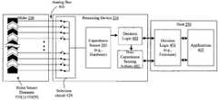
- FIG. 2illustrates a block diagram of one embodiment of an electronic system having a processing device for detecting a presence of a conductive object.
- Electronic system 200includes processing device 210 , touch-sensor pad 220 , touch-sensor slider 230 , touch-sensor buttons 240 , host processor 250 , embedded controller 260 , and non-capacitance sensor elements 270 .
- the processing device 210may include analog and/or digital general purpose input/output (“GPIO”) ports 207 .
- GPIO ports 207may be programmable.
- GPIO ports 207may be coupled to a Programmable Interconnect and Logic (“PIL”), which acts as an interconnect between GPIO ports 207 and a digital block array of the processing device 210 (not illustrated).
- PILProgrammable Interconnect and Logic
- the digital block arraymay be configured to implement a variety of digital logic circuits (e.g., DAC, digital filters, digital control systems) using, in one embodiment, configurable user modules (“UMs”).
- the digital block arraymay be coupled to a system bus (not illustrated).
- Processing device 210may also include memory, such as random access memory (RAM) 205 and program flash 204 .
- RAM 205may be static RAM (SRAM) or the like, and program flash 204 may be a non-volatile storage, or the like, which may be used to store firmware (e.g., control algorithms executable by processing core 202 to implement operations described herein).
- Processing device 210may also include a memory controller unit (MCU) 203 coupled to memory and the processing core 202 .
- MCUmemory controller unit
- the processing device 210may also include an analog block array (not illustrated).
- the analog block arrayis also coupled to the system bus.
- Analog block arrayalso may be configured to implement a variety of analog circuits (e.g., ADC, analog filters) using, in one embodiment, configurable UMs.
- the analog block arraymay also be coupled to the GPIO 207 .
- capacitance sensor 201may be integrated into processing device 210 .
- Capacitance sensor 201may include analog I/O for coupling to an external component, such as touch-sensor pad 220 , touch-sensor slider 230 , touch-sensor buttons 240 , and/or other devices.
- Capacitance sensor 201 and processing device 210are described in more detail below.
- the embodiments described hereinare not limited to touch-sensor pads for notebook implementations, but can be used in other capacitive sensing implementations, for example, the sensing device may be a touch screen, a touch-sensor slider 230 , or a touch-sensor button 240 (e.g., capacitance sensing button). It should also be noted that the embodiments described herein may be implemented in other sensing technologies than capacitive sensing, such as resistive, optical imaging, surface acoustical wave (SAW), infrared, dispersive signal, and strain gauge technologies.
- SAWsurface acoustical wave
- the operations described hereinare not limited to notebook pointer operations, but can include other operations, such as lighting control (dimmer), temperature or environmental control, volume control, graphic equalizer control, speed control, or other control operations requiring gradual or discrete adjustments.
- these embodiments of capacitive sensing implementationsmay be used in conjunction with non-capacitive sensing elements, including but not limited to pick buttons, sliders (ex. display brightness and contrast), scroll-wheels, multi-media control (ex. volume, track advance, etc.) handwriting recognition and numeric keypad operation.
- the electronic system 200includes a touch-sensor pad 220 coupled to the processing device 210 via bus 221 .
- Touch-sensor pad 220may include a two-dimension sensor array.
- the two-dimension sensor arrayincludes multiple sensor elements, organized as rows and columns.
- the electronic system 200includes a touch-sensor slider 230 coupled to the processing device 210 via bus 231 .
- Touch-sensor slider 230may include a single-dimension sensor array.
- the single-dimension sensor arrayincludes multiple sensor elements, organized as rows, or alternatively, as columns.
- the electronic system 200includes touch-sensor buttons 240 coupled to the processing device 210 via bus 241 .
- Touch-sensor button 240may include a single-dimension or multi-dimension sensor array.
- the single- or multi-dimension sensor arrayincludes multiple sensor elements.
- the sensor elementsmay be coupled together to detect a presence of a conductive object over the entire surface of the sensing device.
- the touch-sensor button 240has a single sensor element to detect the presence of the conductive object.
- the touch-sensor button 240may be a capacitance sensor element. Capacitance sensor elements may be used as non-contact sensors. These sensor elements, when protected by an insulating layer, offer resistance to severe environments.
- the electronic system 200may include any combination of one or more of the touch-sensor pad 220 , touch-sensor slider 230 , and/or touch-sensor button 240 .
- the electronic system 200may also include non-capacitance sensor elements 270 coupled to the processing device 210 via bus 271 .
- the non-capacitance sensor elements 270may include buttons, light emitting diodes (LEDs), and other user interface devices, such as a mouse, a keyboard, a display, or other functional keys that do not require capacitance sensing.
- buses 271 , 241 , 231 , and 221may be a single bus. Alternatively, these buses may be configured into any combination of one or more separate buses.
- the processing device 210may also provide value-added functionality such as keyboard control integration, LEDs, battery charger, and general purpose I/O, as illustrated as non-capacitance sensor elements 270 .
- Non-capacitance sensor elements 270are coupled to the GPIO 207 .
- Processing device 210may include internal oscillator/clocks 206 and communication block 208 .
- the oscillator/clocks block 206provides clock signals to one or more of the components of processing device 210 .
- Communication block 208may be used to communicate with an external component, such as a host processor 250 , via host interface (I/F) 251 .
- processing block 210may also be coupled to embedded controller 260 to communicate with the external components, such as host 250 .
- Interfacing to the host 250can be through various methods. In one exemplary embodiment, interfacing with the host 250 may be done using a standard PS/2 interface to connect to an embedded controller 260 , which in turn sends data to the host 250 via a low pin count (LPC) interface.
- LPClow pin count
- interfacingmay be done using a universal serial bus (USB) interface directly coupled to the host 250 via host interface 251 .
- the processing device 210may communicate to external components, such as the host 250 using industry standard interfaces, such as USB, PS/2, inter-integrated circuit (I2C) bus, system packet interfaces (SPI), or the like.
- the host 250 and/or embedded controller 260may be coupled to the processing device 210 with a ribbon or flex cable from an assembly, which houses the sensing device and processing device.
- the processing device 210is configured to communicate with the embedded controller 260 or the host 250 to send and/or receive data.
- the datamay be a command or alternatively a signal.
- the electronic system 200may operate in both standard-mouse compatible and enhanced modes.
- the standard-mouse compatible modeutilizes the HID class drivers already built into the Operating System (OS) software of host 250 . These drivers enable the processing device 210 and sensing device to operate as a standard pointer control user interface device, such as a two-button PS/2 mouse.
- the enhanced modemay enable additional features such as scrolling or disabling the sensing device, such as when a mouse is plugged into the notebook.
- the processing device 210may be configured to communicate with the embedded controller 260 or the host 250 , using non-OS drivers, such as dedicated touch-sensor pad drivers, or other drivers known by those of ordinary skill in the art.
- the processing device 210may operate to communicate data (e.g., commands or signals) using hardware, software, and/or firmware, and the data may be communicated directly to the processing device of the host 250 , such as a host processor, or alternatively, may be communicated to the host 250 via drivers of the host 250 , such as OS drivers, or other non-OS drivers. It should also be noted that the host 250 may directly communicate with the processing device 210 via host interface 251 .
- the data sent to the host 250 from the processing device 210includes click, double-click, movement of the pointer, scroll-up, scroll-down, scroll-left, scroll-right, step Back, and step Forward.
- the data sent to the host 250includes the position or location of the conductive object on the sensing device.
- other user interface device commandsmay be communicated to the host 250 from the processing device 210 . These commands may be based on gestures occurring on the sensing device that are recognized by the processing device, such as tap, push, hop, drag, and zigzag gestures. Alternatively, other commands may be recognized. Similarly, signals may be sent that indicate the recognition of these operations.
- a tap gesturemay be when the finger (e.g., conductive object) is on the sensing device for less than a threshold time. If the time the finger is placed on the touchpad is greater than the threshold time it may be considered to be a movement of the pointer, in the x- or y-axes. Scroll-up, scroll-down, scroll-left, and scroll-right, step back, and step-forward may be detected when the absolute position of the conductive object is within a pre-defined area, and movement of the conductive object is detected.
- Processing device 210may reside on a common carrier substrate such as, for example, an integrated circuit (IC) die substrate, a multi-chip module substrate, or the like. Alternatively, the components of processing device 210 may be one or more separate integrated circuits and/or discrete components. In one exemplary embodiment, processing device 210 may be a Programmable System on a Chip (PSoC®) processing device, developed by Cypress Semiconductor Corporation, San Jose, Calif. Alternatively, processing device 210 may be one or more other processing devices known by those of ordinary skill in the art, such as a microprocessor or central processing unit, a controller, special-purpose processor, digital signal processor (DSP), an application specific integrated circuit (ASIC), a field programmable gate array (FPGA), or the like. In an alternative embodiment, for example, the processing device may be a network processor having multiple processors including a core unit and multiple microengines. Additionally, the processing device may include any combination of general-purpose processing device(s) and special-purpose processing device(s).
- POPProgrammable System
- processing device 210is not limited to having a configuration of a processing device coupled to a host, but may include a system that measures the capacitance on the sensing device and sends the raw data to a host computer where it is analyzed by an application. In effect the processing that is done by processing device 210 may also be done in the host. In another embodiment, the processing device 210 is the host.
- the method and apparatus described hereinmay be implemented in a fully self-contained touch-sensor pad, which outputs fully processed x/y movement and gesture data signals or data commands to a host.
- the method and apparatusmay be implemented in a touch-sensor pad, which outputs x/y movement data and also finger presence data to a host, and where the host processes the received data to detect gestures.
- the method and apparatusmay be implemented in a touch-sensor pad, which outputs raw capacitance data to a host, where the host processes the capacitance data to compensate for quiescent and stray capacitance, and calculates x/y movement and detects gestures by processing the capacitance data.
- the method and apparatusmay be implemented in a touch-sensor pad, which outputs pre-processed capacitance data to a host, where the touchpad processes the capacitance data to compensate for quiescent and stray capacitance, and the host calculates x/y movement and detects gestures from the pre-processed capacitance data.
- the touchpadprocesses the capacitance data to compensate for quiescent and stray capacitance
- the hostcalculates x/y movement and detects gestures from the pre-processed capacitance data.
- other configurationsare possible.
- the electronic system that includes the embodiments described hereinmay be implemented in a conventional laptop touch-sensor pad.
- itmay be implemented in a wired or wireless keyboard integrating a touch-sensor pad, which is itself connected to a host.
- the processing described above as being performed by the “host”may be performed in part or in whole by the keyboard controller, which may then pass fully processed, pre-processed or unprocessed data to the system host.
- the embodimentsmay be implemented in a mobile handset (e.g., cellular or mobile phone) or other electronic devices where the touch-sensor pad may operate in one of two or more modes.
- the touch-sensor padmay operate either as a touch-sensor pad for x/y positioning and gesture recognition, or as a keypad or other arrays of touch-sensor buttons and/or sliders.
- the touch-sensor padalthough configured to operate in the two modes, may be configured to be used only as a keypad.
- Capacitance sensor 201may be integrated into the processing device 210 , or alternatively, in a separate IC. Alternatively, descriptions of capacitance sensor 201 may be generated and compiled for incorporation into other integrated circuits. For example, behavioral level code describing capacitance sensor 201 , or portions thereof, may be generated using a hardware description language, such as VHDL or Verilog, and stored to a machine-accessible medium (e.g., Flash ROM, CD-ROM, hard disk, floppy disk, etc.). Furthermore, the behavioral level code can be compiled into register transfer level (“RTL”) code, a netlist, or even a circuit layout and stored to a machine-accessible medium. The behavioral level code, the RTL code, the netlist, and the circuit layout all represent various levels of abstraction to describe capacitance sensor 201 .
- VHDLhardware description language
- Veriloge.g., Verilog
- electronic system 200may include all the components described above. Alternatively, electronic system 200 may include only some of the components described above, or include additional components not listed herein.
- electronic system 200may be used in a notebook computer.
- the electronic devicemay be used in other applications, such as a mobile handset, a personal data assistant (PDA), a kiosk, a keyboard, a television, a remote control, a monitor, a handheld multi-media device, a handheld video player, a handheld gaming device, or a control panel.
- PDApersonal data assistant
- kioska keyboard
- televisiona remote control
- monitora monitor
- handheld multi-media devicea handheld video player
- handheld gaming devicea control panel
- capacitance sensor 201may be a capacitance sensing relaxation oscillator (CSR).
- CSRcapacitance sensing relaxation oscillator
- the CSRmay be coupled to an array of sensor elements using a current-programmable relaxation oscillator, an analog multiplexer, digital counting functions, and high-level software routines to compensate for environmental and physical sensor element variations.
- the sensor arraymay include combinations of independent sensor elements, sliding sensor elements (e.g., touch-sensor slider), and touch-sensor sensor element pads (e.g., touch pad or touch screen) implemented as a pair of orthogonal sliding sensor elements.
- the CSRmay include physical, electrical, and software components.
- the physical componentsmay include the physical sensor element itself, typically a pattern constructed on a printed circuit board (PCB) with an insulating cover, a flexible membrane, or a transparent overlay.
- PCBprinted circuit board
- the electrical componentmay include an oscillator or other means to convert a capacitance into a measured value.
- the electrical componentmay also include a counter or timer to measure the oscillator output.
- the software componentmay include detection and compensation algorithms to convert the count value into a sensor element detection decision (also referred to as switch detection decision). For example, in the case of slider sensor elements or X-Y touch-sensor sensor element pads, a calculation for finding position of the conductive object to greater resolution than the physical pitch of the sensor elements may be used.
- relaxation oscillatorthere are various known methods for measuring capacitance. Although some embodiments described herein are described using a relaxation oscillator, the present embodiments are not limited to using relaxation oscillators, but may include other methods, such as current versus voltage phase shift measurement, resistor-capacitor charge timing, capacitive bridge divider, charge transfer, sigma-delta modulators, charge-accumulation circuits, or the like.
- the current versus voltage phase shift measurementmay include driving the capacitance through a fixed-value resistor to yield voltage and current waveforms that are out of phase by a predictable amount.
- the drive frequencycan be adjusted to keep the phase measurement in a readily measured range.
- the resistor-capacitor charge timingmay include charging the capacitor through a fixed resistor and measuring timing on the voltage ramp. Small capacitance values may require very large resistors for reasonable timing.
- the capacitive bridge dividermay include driving the capacitor under test through a fixed reference capacitor. The reference capacitor and the capacitor under test form a voltage divider.
- the voltage signalmay be recovered with a synchronous demodulator, which may be done in the processing device 210 .
- the charge transfermay be conceptually similar to an R-C charging circuit.
- C Pis the capacitance being sensed.
- C SUMis the summing capacitor, into which charge is transferred on successive cycles. At the start of the measurement cycle, the voltage on C SUM is discharged. The voltage on C SUM increases exponentially (and only slightly) with each clock cycle. The time for this voltage to reach a specific threshold is measured with a counter. Additional details regarding these alternative embodiments have not been included so as to not obscure the present embodiments, and because these alternative embodiments for measuring capacitance are known by those of ordinary skill in the art.
- FIG. 3Aillustrates a varying capacitance sensor element.
- a capacitance sensor element 300is a pair of adjacent conductors 301 and 302 .
- a conductive object 303e.g., finger
- the capacitance between the electrodes when no conductive object 303 is presentis the base capacitance C P that may be stored as a baseline value.
- the baseline capacitance value C Pmay be subtracted from the total capacitance when the conductive object 303 is present to determine the change in capacitance (e.g., capacitance variation C F ) when the conductive object 303 is present and when the conductive object 303 is not present on the sensor element. Effectively, the capacitance variation C F can be measured to determine whether a conductive object 303 is present or not (e.g., sensor activation) on the sensor element 300 .
- Capacitance sensor element 300may be used in a capacitance sensor array.
- the capacitance sensor arrayis a set of capacitors where one side of each capacitor is connected to a system ground.
- the capacitance sensor element 300is used in the sensor array, when the conductor 301 is sensed, the conductor 302 is connected to ground, and when the conductor 302 is sensed, the conductor 301 is connected to ground.
- the sensor elementis used for a touch-sensor button, the sensor element is sensed and the sensed button area may be surrounded by a fixed ground.
- the presence of the conductive object 303increases the capacitance (C P +C F ) of the sensor element 300 to ground. Determining sensor element activation is then a matter of measuring change in the capacitance (C F ) or capacitance variation.
- Sensor element 300is also known as a grounded variable capacitor.
- the conductive object 303 in this embodimenthas been illustrated as a finger.
- this techniquemay be applied to any conductive object, for example, a conductive door switch, position sensor, or conductive pen in a stylus tracking system (e.g., stylus).
- the capacitance sensor element 300is known as a projected capacitance sensor.
- the capacitance sensor element 300may be a surface capacitance sensor that does not make use of rows or columns, but instead makes use of a single linearized field, such as the surface capacitance sensor described in U.S. Pat. No. 4,293,734.
- the surface capacitance sensormay be used in touch screen applications.
- FIG. 3Billustrates one embodiment of a capacitance sensor element 307 coupled to a processing device 210 .
- Capacitance sensor element 307illustrates the capacitance as seen by the processing device 210 on the capacitance sensing pin 306 .
- a conductive object 303e.g., finger
- C Fcapacitance
- This groundmay be a floating ground.
- C Pcapacitance
- the grounded conductormay be coupled to the processing device 210 using GPIO pin 308 .
- the conductors 305may be metal, or alternatively, the conductors may be conductive ink (e.g., carbon ink), conductive ceramic (e.g., transparent conductors of indium tin oxide (ITO)), conductive polymers, or the like.
- the grounded conductormay be an adjacent sensor element.
- the grounded conductormay be other grounding mechanisms, such as a surrounding ground plane. Accordingly, the processing device 210 can measure the change in capacitance, capacitance variation C F , as the conductive object is in proximity to one of the conductors 305 .
- dielectric material 304Above and below the conductor that is closest to the conductive object 303 is dielectric material 304 .
- the dielectric material 304 above the conductor 305can be an overlay.
- the overlaymay be non-conductive material used to protect the circuitry from environmental conditions and electrostatic discharge (ESD), and to insulate the user's finger (e.g., conductive object) from the circuitry.
- Capacitance sensor element 307may be a sensor element of a touch-sensor pad, a touch-sensor slider, or a touch-sensor button.
- FIG. 3Cillustrates one embodiment of a relaxation oscillator.
- the relaxation oscillator 350is formed by the capacitance to be measured on capacitor 351 , a charging current source 352 , a comparator 353 , and a reset switch 354 (also referred to as a discharge switch).
- capacitor 351is representative of the capacitance measured on a sensor element of a sensor array.
- the relaxation oscillatoris coupled to drive a charging current (Ic) 357 in a single direction onto a device under test (“DUT”) capacitor, capacitor 351 .
- Iccharging current
- DUTdevice under test
- Equation (1)describes the relation between current, capacitance, voltage, and time for a charging capacitor.
- CdVI c dt (1)
- the relaxation oscillatorbegins by charging the capacitor 351 , at a fixed current Ic 357 , from a ground potential or zero voltage until the voltage across the capacitor 351 at node 355 reaches a reference voltage or threshold voltage, V TH 360 .
- V TH 360a reference voltage or threshold voltage
- the relaxation oscillatorallows the accumulated charge at node 355 to discharge (e.g., the capacitor 351 to “relax” back to the ground potential) and then the process repeats itself.
- the output of comparator 353asserts a clock signal F OUT 356 (e.g., F OUT 356 goes high), which enables the reset switch 354 . This discharges the capacitor at node 355 to ground and the charge cycle starts again.
- the relaxation oscillatoroutputs a relaxation oscillator clock signal (F OUT 356 ) having a frequency (f RO ) dependent upon capacitance C of the capacitor 351 and charging current Ic 357 .
- the comparator trip time of the comparator 353 and reset switch 354add a fixed delay.
- the output of the comparator 353is synchronized with a reference system clock to guarantee that the reset time is long enough to completely discharge capacitor 351 .
- f ROchanges proportionally according to Equation (1).
- f REFthe frequency of a known reference system clock signal
- equations (2) and (3) belowdescribe that a change in frequency between F OUT 356 and REF CLK is proportional to a change in capacitance of the capacitor 351 .
- a frequency comparatormay be coupled to receive relaxation oscillator clock signal (F OUT 356 ) and REF CLK, compare their frequencies f RO and f REF , respectively, and output a signal indicative of the difference ⁇ f between these frequencies. By monitoring ⁇ f one can determine whether the capacitance of the capacitor 351 has changed.
- the relaxation oscillator 350may be built using a programmable timer (e.g., 555 timer) to implement the comparator 353 and reset switch 354 .
- the relaxation oscillator 350may be built using other circuitry. Relaxation oscillators are known by those of ordinary skill in the art, and accordingly, additional details regarding their operation have not been included so as to not obscure the present embodiments.
- the capacitor charging current for the relaxation oscillator 350may be generated in a register programmable current output DAC (also known as IDAC).
- the current source 352may be a current DAC or IDAC.
- the IDAC output currentmay be set by an 8-bit value provided by the processing device 210 , such as from the processing core 202 .
- the 8-bit valuemay be stored in a register, in memory, or the like.
- the two “conductors” (e.g., 301 and 302 ) of the sensing capacitorare actually adjacent sensor elements that are electrically isolated (e.g., PCB pads or traces), as indicated in FIG. 3A .
- one of these conductorsis connected to a system ground.
- Layouts for touch-sensor slider (e.g., linear slide sensor elements) and touch-sensor pad applicationshave sensor elements that may be immediately adjacent. In these cases, all of the sensor elements that are not active are connected to a system ground through the GPIO 207 of the processing device 210 dedicated to that pin.
- equation (4)The dimensions of equation (4) are in meters. This is a very simple model of the capacitance. The reality is that there are fringing effects that substantially increase the sensor element-to-ground (and PCB trace-to-ground) capacitance.
- a baseline update routinewhich compensates for this variation, may be provided in the high-level APIs.
- the relaxation oscillator output signal 356may be fed to a digital counter for measurement. There are two methods for counting the relaxation oscillator output signal 356 : frequency measurement and period measurement. Additional details of the relaxation oscillator and digital counter are known by those of ordinary skill in the art, and accordingly a detailed description regarding them has not been included.
- the embodiments described hereinare not limited to using relaxation oscillators, but may include other sensing circuitry for measuring capacitance, such as versus voltage phase shift measurement, resistor-capacitor charge timing, capacitive bridge divider, charge transfer, sigma-delta modulators, charge-accumulation circuits, or the like.
- FIG. 3Dillustrates a schematic of one embodiment of a circuit 375 including a sigma-delta modulator 360 and a digital filter 390 for measuring capacitance on a sensor element 351 .
- Circuit 375includes a switching circuit 370 , switching clock source 380 , sigma-delta modulator 360 , and digital filter 390 for measuring the capacitance on sensor element 351 .
- Sensor element 351may be a sensor element of a sensor array, and is represented as a switching capacitor C X in the modulator feedback loop. Alternatively, sensor element 351 may be a single sensor element, such as used in a touch-sensor button.
- Switching circuit 370includes two switches Sw 1 371 and Sw 2 372 .
- the switches Sw 1 371 and Sw 2 372operate in two, non-overlapping phases (also known as break-before-make configuration). These switches together with sensing capacitor C x 351 form the switching capacitor equivalent resistor, which provides the modulator capacitor C mod 363 of sigma-delta modulator 360 charge current (as illustrated in FIG. 3D ) or discharge current (not illustrated) during one of the two phases.
- the sigma-delta modulator 360includes the comparator 361 , latch 362 , modulator capacitor C mod 363 , modulator feedback resistor 365 , which may also be referred to as bias resistor 365 , and voltage source 366 .
- the output of the comparatormay be configured to toggle when the voltage on the modulator capacitor 363 crosses a reference voltage 364 .
- the reference voltage 364may be a pre-programmed value, and may be configured to be programmable.
- the sigma-delta modulator 360also includes a latch 362 coupled to the output of the comparator 361 to latch the output of the comparator 361 for a given amount of time, and provide as an output, output 392 .
- the latchmay be configured to latch the output of the comparator based on a clock signal from the gate circuit 382 (e.g., oscillator signal from the oscillator 381 ).
- the sigma-delta modulator 360includes a synchronized latch that operates to latch an output of the comparator for a pre-determined length of time. The output of the comparator may be latched for measuring or sampling the output signal of the comparator 361 by the digital filter 390 .
- Sigma-delta modulator 360is configured to keep the voltage on the modulator capacitor 363 close to reference voltage V ref 364 by alternatively connecting the switching capacitor resistor (e.g., switches Sw 1 371 and Sw 2 372 and sensing capacitor C x 351 ) to the modulator capacitor 363 .
- the output 392 of the sigma-delta modulator 360(e.g., output of latch 362 ) is feedback to the switching clock circuit 380 , which controls the timing of the switching operations of switches Sw 1 371 and Sw 2 372 of switching circuit 370 .
- the switching clock circuit 380includes an oscillator 381 and gate 382 .
- the switching clock circuit 380may include a clock source, such as a spread spectrum clock source (e.g., pseudo-random signal (PRS)), a frequency divider, a pulse width modulator (PWM), or the like.
- the output 392 of the sigma-delta modulator 360is used with an oscillator signal to gate a control signal 393 , which switches the switches Sw 1 371 and Sw 2 372 in a non-overlapping manner (e.g., two, non-overlapping phases).
- the output 392 of the sigma-delta modulator 360is also output to digital filter 390 , which filters and/or converts the output into the digital code 391 .
- the modulator capacitor 363has zero voltage and switching capacitor resistor (formed by sensing capacitor Cx 351 , and switches Sw 1 371 and Sw 2 372 ) is connected between Vdd line 366 and modulator capacitor 363 .
- This connectionallows the voltage on the modulator capacitor 363 to rise.
- the comparator 361toggles and gates the control signal 393 of the switches Sw 1 371 and Sw 2 372 , stopping the charge current. Because the current via bias resistors R b 365 continues to flow, the voltage on modulator capacitor 363 starts dropping. When it drops below the reference voltage 364 , the output of the comparator 361 switches again, enabling the modulator capacitor 363 to start charging.
- the latch 362 and the comparator 361set the sample frequency of the sigma-delta modulator 360 .
- the digital filter 390is coupled to receive the output 392 of the sigma-delta modulator 360 .
- the output 392 of the sigma-delta modulator 360may be a single bit bit-stream, which can be filtered and/or converted to numerical values using a digital filter 390 .
- the digital filter 390is a counter.
- the standard Sinc digital filtercan be used.
- the digital filteris a decimator.
- other digital filtersmay be used for filtering and/or converting the output 392 of the sigma-delta modulator 360 to provide the digital code 391 .
- the output 392may be output to the decision logic 402 or other components of the processing device 210 , or to the decision logic 451 or other components of the host 250 to process the bitstream output of the sigma-delta modulator 360 .
- the sigma-delta modulator 360keeps these currents equal in the average by keeping the voltage on the modulator 363 equal to, or close to, the reference voltage V ref 364 .
- the current of the bias resistor R b 365is:
- Equation (8)can be rewritten in the following form:
- Equation (10)determines the minimum sensing capacitance value, which can be measured with the proposed method at given parameters set:
- the resolution of this methodmay be determined by the sigma-delta modulator duty cycle measurement resolution, which is represented in the following equations:
- the duty cyclehas a 12-bit resolution and the capacitance resolution is 0.036 pF.
- ⁇ s0.1 microseconds
- other types of digital filtersmay be used, for example, by using the Sinc 2 filter, the scanning time at the same resolution may be reduced approximately 4 times. To do this the sensing method should have suitable measurement speed.
- a good measurement ratemay be accomplished by using a double integrator as the digital filter 390 .
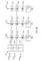
- FIG. 4Aillustrates a block diagram of one embodiment of an electronic device 400 including a processing device 210 that includes a capacitance sensor 201 for measuring the capacitance on a touch panel 410 in a first mode 430 .
- the electronic device 400includes the touch panel 410 , which includes multiple touch-sensor buttons (e.g., similar to touch-sensor buttons 240 of FIG. 2 ), processing device 210 , and host 250 .
- Touch panel 410includes sensor elements 355 ( 1 )- 355 (N), where N is a positive integer value that represents the number of touch-sensor buttons of the touch panel 410 .
- Each sensor element 355corresponds to a button of the touch panel 410 .
- the buttonsare described as being part of a touch panel, alternatively, the buttons may be separated in multiple touch panels or the buttons may be individually mounted on the device without the use of a touch panel.
- the sensor elements 355 ( 1 )- 355 (N) of touch panel 410are coupled to multiple pins of the processing device 210 via an analog bus 401 . Each of the sensor elements 355 are coupled to a pin on the processing device 210 .
- the analog bus 401is coupled to a selection circuit 420 .
- the selection circuit 420may be configured to couple the sensor elements 355 individually to the capacitance sensor 201 during the first mode 430 (illustrated in FIG. 4A ), and configured to collectively couple a group of sensor elements to the capacitance sensor 201 during the second mode 440 (illustrated in FIG. 4B ). For example in the first mode 430 , as illustrated in FIG.
- the first sensor element 355 ( 1 )is selected (as indicated by the black sensor element of the touch panel 410 ), and coupled to the capacitance sensor 201 to measure the capacitance on the first sensor element 355 ( 1 ).
- the selection circuit 420opens the switch that connects the first sensor element 355 ( 1 ) to the capacitance sensor 201 , and closes another switch that connects the capacitance sensor 201 to a subsequent sensor element. This is repeated to individually measure the capacitance on each of the sensor elements 355 during the first mode 430 .
- the processing device 210is configured to perform a capacitance measurement on each of the sensor elements 355 ( 1 )- 355 (N) during each sensing interval when in the first mode 430 .
- the selection circuit 420is configured to sequentially select the individual sensor elements. In another embodiment, the selection circuit 420 is configured to sequentially select sets of sensor elements, such as rows or columns, as described below.
- the selection circuit 420may be configured to provide charge current or voltage to the selected sensor elements and to measure a capacitance on the selected sensor elements. In one exemplary embodiment, the selection circuit 420 is a multiplexer array. Alternatively, the selection circuit may be other circuitry inside or outside the capacitance sensor 201 to select the sensor element(s) to be measured.
- the capacitance sensor 201may be used to measure capacitance on all or less than all of the sensor elements of the touch panel 410 .
- multiple capacitance sensors 201may be used to measure capacitance on all or less than all of the sensor elements of the touch panel 410 .
- the selection circuit 420is configured to connect the sensor elements that are not being measured to the system ground. This may be done in conjunction with a dedicated pin in the GPIO port 207 .
- the processing device 210further includes a decision logic block 402 .
- the operations of decision logic block 402may be implemented in firmware; alternatively, it may be implemented in hardware or software.
- the decision logic block 402may be configured to receive the digital code or counts from the capacitance sensor 201 , and to determine the state of the touch panel 410 , such as whether a conductive object is detected on the touch panel 410 , which button has been pressed on the touch panel 410 , or the like.
- the processing device 201may send the raw data to the host 250 , as described above.
- Host 250may include decision logic 451 .
- the operations of decision logic 451may also be implemented in firmware, hardware, and/or software.
- the hostmay include high-level APIs in applications 452 that perform routines on the received data, such as compensating for sensitivity differences, other compensation algorithms, baseline update routines, start-up and/or initialization routines, interpolations operations, scaling operations, or the like.
- the operations described with respect to the decision logic 402may be implemented in decision logic 451 , applications 452 , or in other hardware, software, and/or firmware external to the processing device 210 .
- the processing device 210may also include a non-capacitance sensing actions block 403 .
- This blockmay be used to process and/or receive/transmit data to and from the host 250 .
- additional componentsmay be implemented to operate with the processing device 210 along with the touch panel 410 (e.g., keyboard, keypad, mouse, trackball, LEDs, displays, or the like).
- the sensor elementse.g., capacitors 355 ( 1 )-(N)
- the digital code or count values for each sensor element with no activationare stored as a baseline array (C P ).
- the presence of a finger on the sensor elementis determined by the difference in counts between a stored value for no sensor element activation and the acquired value with sensor element activation, referred to here as ⁇ n.
- the sensitivity of a single sensor elementis approximately:
- ⁇ nshould be large enough for reasonable resolution and clear indication of sensor element activation. This drives sensor element construction decisions.
- C Fshould be as large a fraction of C P as possible. Since C F is determined by finger area and distance from the finger to the sensor element's conductive traces (through the over-lying insulator), the baseline capacitance C P should be minimized.
- the baseline capacitance C Pincludes the capacitance of the sensor element pad plus any parasitics, including routing and chip pin capacitance.
- the first mode 430is a normal mode of operation of the electronic device 400 .
- the first mode 430is a “fine” measurement mode and is when the electronic device is active, as opposed to being in “sleep” mode (as described below).
- FIG. 4Billustrates the electronic device 400 of FIG. 4A in a second mode 440 .
- the selection circuit 420is configured to couple all of the sensor elements 355 ( 1 )- 355 (N) to the capacitance sensor 201 using individual switches. Instead of measuring the capacitance on each of the sensor elements individually as done in the first mode 430 , the capacitance sensor 201 collectively measures a total aggregate capacitance on the coupled sensor elements 355 ( 1 )- 355 (N) in the second mode 440 . For example, as illustrated in FIG.
- all the sensor elements 355 ( 1 )-(N)are selected (as indicated by the black sensor elements of the touch panel 410 ), and coupled to the capacitance sensor 201 to collectively measure the capacitance on all the sensor elements 355 ( 1 )- 355 (N).
- the processing device 210is configured to perform a single capacitance measurement on all the sensor elements 355 ( 1 )- 355 (N) during each sensing interval when in the second mode 440 .
- FIGS. 4A and 4Billustrate all the sensor elements 355 ( 1 )- 355 (N) being coupled together during the second mode 440
- a fraction of all the sensor elements 355 ( 1 )- 355 (N)may be coupled together during the second mode 440 .
- the processing device 210may be configured to individually measure a capacitance on each of the sensor elements 355 ( 1 )- 355 (N) of the electronic device 400 in the first mode 430 .
- the processing device 210may also be configured to couple a group of (e.g., all or a fraction of) the sensor elements 355 ( 1 )-(N), and collectively measure an aggregate capacitance on the group of sensor elements in the second mode 440 .
- the group of sensor elementsmay be coupled together and the aggregate capacitance measured when a presence of a conductive object is not detected on the sensor elements during the first mode 430 (e.g., no conductive object is detected while individually measuring the capacitance on each of the sensor elements).
- the electronic device 400may be placed in a “sleep” mode (e.g., reduced power mode) when the conductive object is not present on the electronic device 400 .
- the electronic device 400may be placed in the “sleep” mode after a certain number of individual sensing cycles have resulted in no conductive object being detected on the electronic device 400 .
- “sleep” modee.g., second mode 440
- the electronic device 400can periodically scan the group of coupled sensor elements to determine if a conductive object is present on the electronic device 400 .
- the electronic device 400When the electronic device 400 detects the presence of the conductive object in “sleep” mode (e.g., conductive object is detected while collectively measuring a capacitance on the group of sensor elements), the electronic device 400 may be placed in a normal or active mode (e.g., first mode 430 ).
- a normal or active modee.g., first mode 430
- the electronic device 400continues to individually measure the capacitance on each of the sensor elements and is placed in the “sleep” mode (e.g., second mode 440 ) for a period of time when the conductive object is not present on the device during the first mode 430 .
- the electronic device 400may be placed in the “sleep” mode (e.g., second mode 440 ) after the electronic device 400 has not detected a conductive object on the device after a predetermined period of time.
- the electronic device 400may be placed in the “sleep” mode after the electronic device 400 has not detected a conductive object on the device after a certain number, N, individual sensing cycles.
- Nnumber
- the electronic device 400In the second mode 440 , the electronic device 400 collectively measures a capacitance on the group of sensor elements after the period of time has lapsed. If the electronic device 400 does not detect a presence of a conductive object during the second mode 440 , the electronic device 400 may sleep for another period of time. After this period of time, the electronic device 400 wakes and collectively measures a capacitance on the group of sensor elements. Once the electronic device 400 detects a presence of the conductive object during the second mode 440 , the electronic device 400 transitions to the first mode 430 to individually measure a capacitance on each of the sensor elements.
- the processing device 210while in the second mode 440 , performs a baseline measurement on the group of sensor elements after the group of sensor elements are coupled together.
- the baseline measurementmay be representative of the capacitance on the group of sensor elements when a conductive object is not present on the electronic device 400 .
- the baseline measurementmay be measured to account for parasitic capacitance in the device.
- the baseline measurementmay be compared against the capacitance measurements made during the second mode 440 . For example, when the group of sensor elements is subsequently measured, if the collectively measured capacitance on the group of sensor elements is greater than the baseline measurement, then a presence of a conductive object is detected on the electronic device. If the collectively measured capacitance is greater than the baseline measurement, the electronic device 400 may transition to the first mode 430 to individually measure a capacitance on each of the sensor elements.
- the collectively measured capacitancecan be compared to a threshold above the baseline measurement. For example, if the collectively measured capacitance is greater than the threshold above the baseline measurement, then a presence of a conductive object is detected, and the electronic device 400 can transition to the first mode 430 to individually measure the capacitance on each of the sensor elements. Conversely, if the collective measured capacitance is less than the baseline measurement or less than the threshold above the baseline measurement, then a presence of a conductive object is not detected, and the electronic device 400 remains in the second mode 440 . The electronic device 400 may be placed in the “sleep” mode for a period of time if the collectively measured capacitance on the group sensor elements is equal to or less than the baseline measurement or the threshold above the baseline measurement.
- the electronic device 400transitions from the first mode 430 to the second mode 440 when the presence of the conductive object is not detected on the sensor elements while individually measuring the capacitance on each of the sensor elements in the first mode 430 . In another embodiment, the electronic device 400 transitions from the second mode 440 to the first mode 430 when the presence of the conductive object is detected on the group of sensor elements while collectively measuring the capacitance on the group of sensor elements in the second mode 440 . As described above, the group of sensor elements may include all or a fraction of the sensor elements 355 .
- FIG. 5illustrates a block diagram of one embodiment of an electronic device 500 including a processing device 210 that includes capacitance sensors 201 for measuring the capacitance on a slider 230 .
- the electronic device 500is similar to the electronic device 400 , except the processing device 210 is coupled to the slider 230 via the selection circuit 420 , instead of the touch panel 410 .
- the slider 230 of FIG. 5includes multiple sensor elements 555 ( 1 )- 555 (N), where N is a positive integer value that represents the number of sensor elements.
- the slider 230may be a single-dimension sensor array including the sensor elements 555 ( 1 )- 555 (N).
- the single-dimension sensor arraymay provide output data to the analog bus 401 of the processing device 210 (e.g., via lines 231 of FIG. 2 ).
- the slider 230may be used for control requiring gradual or discrete adjustments. Examples include a lighting control (dimmer), temperature control, volume control, graphic equalizer, and speed control. Slider controls may also be used for scrolling functions in menus of data.
- These sensor elementsmay be mechanically adjacent to one another. Activation of one sensor element may result in partial activation of physically adjacent sensor elements. The actual position in the sliding sensor element is found by computing the centroid location of the set of sensor elements activated, as described below.
- the decision logic block 402may be configured to receive the digital code or counts from the capacitance sensor 201 , and to determine the state of the slider 230 , such as whether a conductive object is detected on the slider 230 , such as which sensor element has been pressed, where the conductive object was detected on the slider 230 (e.g., determining the X-, Y-coordinates of the presence of the conductive object), determining absolute or relative position of the conductive object, whether the conductive object is performing a pointer operation, whether a gesture has been recognized on the slider 230 (e.g., click, double-click, movement of the pointer, scroll-up, scroll-down, scroll-left, scroll-right, step Back, step Forward, tap, push, hop, zigzag gestures, et), or the like.
- the state of the slider 230such as whether a conductive object is detected on the slider 230 , such as which sensor element has been pressed, where the conductive object was detected on the slider 230 (e.
- the selection circuit 420is configured to couple each of the sensor elements to the capacitance sensor 201 of the processing device either individually for sequential measurements of the sensor elements in the first mode 430 or collectively for measurements of the coupled sensor elements in the second mode 440 .
- half of the sensor elements 555 ( 1 )- 555 (N)are selected (as indicated by the black sensor elements of the slider 230 ) in the second mode 440 , and coupled to the capacitance sensor 201 to measure the aggregate capacitance on the coupled sensor elements.
- each of the sensor elements 555 ( 1 )- 555 (N)are sequentially selected and coupled to the capacitance sensor 201 of the processing device 210 to individually measure the capacitance on each of the sensor elements 555 ( 1 )- 555 (N).
- the processing device 210is configured to perform a capacitance measurement on each of the sensor elements 555 ( 1 )- 555 (N) during each sensing interval when in the first mode 430 , and to perform a single capacitance measurement on the coupled sensor elements 555 ( 1 )- 555 (N) (e.g., half of the sensor elements) during each sensing interval when in the second mode 440 .
- FIG. 5illustrate half of the sensor elements 555 ( 1 )- 555 (N) being coupled together during the second mode 440
- other fractions or all of the sensor elements 555 ( 1 )- 555 (N)may be coupled together during the second mode 440 .
- Coupling less than all of the sensor elements (e.g., a fraction of all the sensor elements) in the second mode 440may have the advantage of reducing the background parasitic capacitance to ground in the electronic device 500 , and thus reduce the time taken to make the single measurement in the second mode 440 , as compared to coupling all the sensor elements, and thus further reduce the sleep current
- FIG. 6illustrates a block diagram of one embodiment of an electronic device 600 including a processing device 210 that includes two capacitance sensors 201 for measuring the capacitance on a sensor array 610 .
- the electronic device 600is similar to the electronic devices 400 and 500 , except the processing device 210 is coupled to the sensor array 610 using two selection circuits 420 and 620 and two capacitance sensors 201 .
- the sensor array 610is implemented in the touch-sensor pad 220 , as described with respect to FIG. 2 .
- the sensor array 610may be implemented in other capacitance sensing devices.
- the sensor array 610is a two-dimension sensor array including the sensor elements 655 ( 1 )- 655 (N), where N is a positive integer value that represents the number of sensor elements of the two-dimension sensor array.
- the two-dimension sensor array 610may provide output data to the analog bus 401 of the processing device 210 (e.g., via bus 221 ).
- the sensing array 610may be used for similar operation as described above with respect to the touch-sensor pad 220 .
- the decision logic block 402may be configured to receive the digital code or counts from the capacitance sensor 201 , and to determine the state of the sensor array 610 , such as whether a conductive object is detected on the sensor array 610 , which sensor element of the sensor array 610 has been pressed, where the conductive object was detected on the sensor array 610 (e.g., determining the X-, Y-coordinates of the presence of the conductive object), determining absolute or relative position of the conductive object, whether the conductive object is performing a pointer operation, whether a gesture has been recognized on the sensor array 610 (e.g., click, double-click, movement of the pointer, scroll-up, scroll-down, scroll-left, scroll-right, step Back, step Forward, tap, push, hop, zigzag gestures, etc), or the like.
- the selection circuit 420is configured to couple each of the sensor elements to the capacitance sensor 201 of the processing device either individually for sequential measurements of the sensor elements in the first mode 430 or collectively for measurements of the coupled sensor elements in the second mode 440 .
- the selection circuits 420 and 620are configured to couple each of the sensor elements to the capacitance sensors 201 as sets of sensor elements, such as a row or column of sensor elements.
- the selection circuits 420 and 620are configured to substantially simultaneously measure two sets of sensor elements at a time. For example, as illustrated in FIG.
- a first row 601 and a first column 602are selected in the first mode 430 , and coupled to the capacitance sensors 201 , respectively, to individually measure the capacitance on the first row and the first column of sensor elements.
- the selection circuits 420 and 620each open the switch that connects the respective capacitance sensor 201 to the first row 601 and first column 602 , and closes another switch that connects the respective capacitance sensor 201 to a subsequent row and a subsequent column, respectively. This is repeated to individually measure the capacitance on each of the rows and each of the columns of the sensor array 610 during the first mode 430 .
- the processing device 210is configured to perform a capacitance measurement on each of the rows and columns during each sensing interval when in the first mode 430 . However, in the second mode 440 , all of the rows are coupled together to collectively measure an aggregate capacitance on the rows of the sensor array 610 . Similarly, in the second mode 440 , all of the columns are coupled together to collectively measure an aggregate capacitance on the columns of the sensor array 610 . In one embodiment, the processing device 210 is configured to perform a single capacitance measurement on all the rows of the sensor array 610 during each sensing interval when in the second mode 440 .
- the processing device 210is configured to perform a single capacitance measurement on all the columns of the sensor array 610 during each sensing interval when in the second mode 440 .
- the processing device 210is configured to perform both measurements of the all the rows and all the columns during each sensing interval when in the second mode 440 .
- FIG. 6illustrates all of the rows or all of the columns of the sensor array 610 being coupled together during the second mode 440
- fractions of all of the rows or fractions of all of the columnsmay be coupled together during the second mode 440 .
- half of the columnsare coupled together and coupled to the first capacitance sensor 201
- half of the rowsare coupled together and coupled to the second capacitance sensor 201 .
- Coupling less than all of the rows and/or columns (e.g., a fraction of all the rows or columns of sensor elements) in the second mode 440may have the advantage of reducing the background parasitic capacitance to ground in the electronic device 600 , and thus reduce the time taken to make the capacitance measurement(s) in the second mode 440 , as compared to coupling all the rows and/or all the columns of sensor elements.
- the sensor arraymay be a grid-like pattern of sensor elements (e.g., capacitive elements) used in conjunction with the processing device 210 to detect a presence of a conductive object, such as a finger, to a resolution greater than that which is native.
- the touch-sensor pad layout patternmay be disposed to maximize the area covered by conductive material, such as copper, in relation to spaces necessary to define the rows and columns of the sensor array.
- the arrayis first scanned to verify that a given sensor element location is valid. The requirement is for some number of adjacent sensor element signals to be above a noise threshold. When the strongest signal is found, this signal and those immediately adjacent are used to compute a centroid:
- Centroidn i - 1 ⁇ ( i - 1 ) + n i ⁇ i + n i + 1 ⁇ ( i + 1 ) n i - 1 + n i ⁇ i + n i + 1 ( 15 )
- the calculated valuemay be fractional.
- the centroid valuemay be multiplied by a calculated or predetermined scalar. It may be more efficient to combine the interpolation and scaling operations into a single calculation and report this result directly in the desired scale. This may be handled in the high-level APIs. Alternatively, other methods may be used to interpolate the position of the conductive object.
- FIG. 7illustrates a flow chart of one embodiment of a method 700 for coupling a group of sensor elements together when in a reduced power mode.
- Method 700starts in operation 701 , and starts to measure a capacitance on each of the sensor elements in turn, operation 702 .
- the processing device 210then performs conductive object detection algorithms, operation 703 .
- the detection algorithmsmay include whether a presence of the conductive object is present on the device, which sensor element, and corresponding button, has been activated, which the location of the presence of the conductive object on the device, whether a gesture is recognized, or the like.
- the method 700determines whether a conductive object detection algorithm detected the presence of the conductive object, operation 704 .
- the processing device 210sends button press data to the host 250 , and returns to measure a capacitance of each sensor element in turn in operation 702 .
- the processing device 210connects all (or a fraction of all) of the sensor elements together, operation 706 . This may be done using the selection circuit 420 .
- a baseline measurementis performed, operation 707 .
- the baseline measurementis representative of the aggregate capacitance on the coupled sensor elements when no conductive object is present on the device.
- the baseline measurementaccounts for the parasitic capacitance of the coupled sensor elements.
- the capacitanceis collectively measured on the coupled sensor elements, operation 708 .
- the method 700determines if the collective capacitance is greater than the baseline measurement performed in operation 707 , operation 709 .
- a threshold above the baseline measurementmay be used. If the collective capacitance is greater than the baseline measurement or the threshold above the baseline measurement, the method returns to measuring a capacitance of each of the sensor elements in turn of operation 702 .
- the method 700places the device in the reduced power mode (e.g., “sleep” mode) for a period of time (e.g., 100 ms), operation 710 . After the period of time has lapsed, the device wakes and measures the collective capacitance again in operation 708 . This process is repeated until a presence of a conductive object is detecting using the group of sensor elements. Once the conductive object is detected, then the method returns to individually measuring each of the sensor elements.
- the reduced power modee.g., “sleep” mode
- a period of timee.g. 100 ms
- the methodincludes individually measuring a capacitance on each of the sensor elements of a touch-sensor device in a first mode, and collectively measuring the capacitance on the group of sensor elements in a second mode.
- the second modemay be a lower power mode than the first mode.
- the second modeincludes a reduced power mode that allows the power in the device to be reduced as compared to when the device is in the first mode.
- the methodincludes individually measuring a capacitance on each of the sensor elements of a touch-sensor device.
- the methodalso includes coupling together a group of sensor elements, such as all of or a fraction of all of the sensor elements of the device when a presence of a conductive object is not detected on the sensor elements while individually measuring a capacitance on each of the sensor elements.
- the methodincludes collectively measuring a capacitance on the group of sensor elements. This may be done to reduce the amount of power consumption to determine if a conductive object is present or not on the device.
- the devicecan be placed in a reduced power mode for a period of time, periodically waking to make a coarse measurement of whether a conductive object is present or not. This reduces the power consumption of the device.
- the methodincludes transitioning from the first mode to the second mode when the presence of the conductive object is not detected on the sensor elements while individually measuring the capacitance on each of the sensor elements in the first mode.
- the methodmay also include transitioning from the second mode to the first mode when the presence of the conductive object is detected on the group of sensor elements while collectively measuring the capacitance on the group of sensor elements in the second mode.
- the methodincludes transitioning to the second mode from the first mode when a presence of a conductive object is not detected after a period of time in the first mode.
- Embodiments of the present inventioninclude various operations. These operations may be performed by hardware components, software, firmware, or a combination thereof.
- the term “coupled to”may mean coupled directly or indirectly through one or more intervening components. Any of the signals provided over various buses described herein may be time multiplexed with other signals and provided over one or more common buses. Additionally, the interconnection between circuit components or blocks may be shown as buses or as single signal lines. Each of the buses may alternatively be one or more single signal lines and each of the single signal lines may alternatively be buses.
- Certain embodimentsmay be implemented as a computer program product that may include instructions stored on a machine-readable medium. These instructions may be used to program a general-purpose or special-purpose processor to perform the described operations.
- a machine-readable mediumincludes any mechanism for storing or transmitting information in a form (e.g., software, processing application) readable by a machine (e.g., a computer).
- the machine-readable mediummay include, but is not limited to, magnetic storage medium (e.g., floppy diskette); optical storage medium (e.g., CD-ROM); magneto-optical storage medium; read-only memory (ROM); random-access memory (RAM); erasable programmable memory (e.g., EPROM and EEPROM); flash memory; electrical, optical, acoustical, or other form of propagated signal (e.g., carrier waves, infrared signals, digital signals, etc.); or another type of medium suitable for storing electronic instructions.
- magnetic storage mediume.g., floppy diskette
- optical storage mediume.g., CD-ROM
- magneto-optical storage mediume.g., magneto-optical storage medium
- ROMread-only memory
- RAMrandom-access memory
- EPROM and EEPROMerasable programmable memory
- flash memoryelectrical, optical, acoustical, or other form of propagated signal (e.g., carrier waves, in
- some embodimentsmay be practiced in distributed computing environments where the machine-readable medium is stored on and/or executed by more than one computer system.
- the information transferred between computer systemsmay either be pulled or pushed across the communication medium connecting the computer systems.
Landscapes
- Engineering & Computer Science (AREA)
- Theoretical Computer Science (AREA)
- General Engineering & Computer Science (AREA)
- Physics & Mathematics (AREA)
- General Physics & Mathematics (AREA)
- Human Computer Interaction (AREA)
- Computer Hardware Design (AREA)
- Position Input By Displaying (AREA)
Abstract
Description
CdV=Icdt (1)
ΔC∝Δf, where (2)
Δf=fRO−fREF. (3)
The
where fsis the operation frequency of the switches (e.g., switching circuit370). If the
In the operation mode,
or taking into account that the
The Equation (8) can be rewritten in the following form:
or after rewriting relatively ΔCx, we obtain:
Claims (32)
Priority Applications (5)
| Application Number | Priority Date | Filing Date | Title |
|---|---|---|---|
| US11/801,115US8144126B2 (en) | 2007-05-07 | 2007-05-07 | Reducing sleep current in a capacitance sensing system |
| US13/049,556US8976124B1 (en) | 2007-05-07 | 2011-03-16 | Reducing sleep current in a capacitance sensing system |
| US14/606,767US9575606B1 (en) | 2007-05-07 | 2015-01-27 | Reducing sleep current in a capacitance sensing system |
| US16/130,235US10788937B2 (en) | 2007-05-07 | 2018-09-13 | Reducing sleep current in a capacitance sensing system |
| US16/990,933US12181943B2 (en) | 2007-05-07 | 2020-08-11 | Reducing sleep current in a capacitance sensing system |
Applications Claiming Priority (1)
| Application Number | Priority Date | Filing Date | Title |
|---|---|---|---|
| US11/801,115US8144126B2 (en) | 2007-05-07 | 2007-05-07 | Reducing sleep current in a capacitance sensing system |
Related Child Applications (1)
| Application Number | Title | Priority Date | Filing Date |
|---|---|---|---|
| US13/049,556ContinuationUS8976124B1 (en) | 2007-05-07 | 2011-03-16 | Reducing sleep current in a capacitance sensing system |
Publications (2)
| Publication Number | Publication Date |
|---|---|
| US20080277171A1 US20080277171A1 (en) | 2008-11-13 |
| US8144126B2true US8144126B2 (en) | 2012-03-27 |
Family
ID=39968504
Family Applications (5)
| Application Number | Title | Priority Date | Filing Date |
|---|---|---|---|
| US11/801,115Active2029-10-12US8144126B2 (en) | 2007-05-07 | 2007-05-07 | Reducing sleep current in a capacitance sensing system |
| US13/049,556Active2028-10-12US8976124B1 (en) | 2007-05-07 | 2011-03-16 | Reducing sleep current in a capacitance sensing system |
| US14/606,767ActiveUS9575606B1 (en) | 2007-05-07 | 2015-01-27 | Reducing sleep current in a capacitance sensing system |
| US16/130,235ActiveUS10788937B2 (en) | 2007-05-07 | 2018-09-13 | Reducing sleep current in a capacitance sensing system |
| US16/990,933Active2027-12-12US12181943B2 (en) | 2007-05-07 | 2020-08-11 | Reducing sleep current in a capacitance sensing system |
Family Applications After (4)
| Application Number | Title | Priority Date | Filing Date |
|---|---|---|---|
| US13/049,556Active2028-10-12US8976124B1 (en) | 2007-05-07 | 2011-03-16 | Reducing sleep current in a capacitance sensing system |
| US14/606,767ActiveUS9575606B1 (en) | 2007-05-07 | 2015-01-27 | Reducing sleep current in a capacitance sensing system |
| US16/130,235ActiveUS10788937B2 (en) | 2007-05-07 | 2018-09-13 | Reducing sleep current in a capacitance sensing system |
| US16/990,933Active2027-12-12US12181943B2 (en) | 2007-05-07 | 2020-08-11 | Reducing sleep current in a capacitance sensing system |
Country Status (1)
| Country | Link |
|---|---|
| US (5) | US8144126B2 (en) |
Cited By (61)
| Publication number | Priority date | Publication date | Assignee | Title |
|---|---|---|---|---|
| US20080246723A1 (en)* | 2007-04-05 | 2008-10-09 | Baumbach Jason G | Integrated button activation sensing and proximity sensing |
| US20090064809A1 (en)* | 2007-09-07 | 2009-03-12 | Lear Corporation | Rotary control knob assembly |
| US20100060301A1 (en)* | 2007-11-27 | 2010-03-11 | Frederick Johannes Bruwer | Noise rejection |
| US20100328255A1 (en)* | 2009-06-30 | 2010-12-30 | Sony Corporation | Touch detection device and display device having touch sensor function |
| US20110074609A1 (en)* | 2009-09-28 | 2011-03-31 | Microchip Technology Incorporated | Capacitive key touch sensing using analog inputs and digital outputs |
| US20130147732A1 (en)* | 2008-01-28 | 2013-06-13 | Cypress Semiconductor Corporation | Touch sensing |
| US8493351B2 (en) | 2006-03-30 | 2013-07-23 | Cypress Semiconductor Corporation | Apparatus and method for reducing average scan rate to detect a conductive object on a sensing device |
| US8570052B1 (en) | 2008-02-27 | 2013-10-29 | Cypress Semiconductor Corporation | Methods and circuits for measuring mutual and self capacitance |
| US8570053B1 (en) | 2007-07-03 | 2013-10-29 | Cypress Semiconductor Corporation | Capacitive field sensor with sigma-delta modulator |
| US8692563B1 (en) | 2008-02-27 | 2014-04-08 | Cypress Semiconductor Corporation | Methods and circuits for measuring mutual and self capacitance |
| US20150049032A1 (en)* | 2010-06-16 | 2015-02-19 | Martin J. SIMMONS | Touch-Screen Panel with Multiple Sense Units and Related Methods |
| US8976124B1 (en) | 2007-05-07 | 2015-03-10 | Cypress Semiconductor Corporation | Reducing sleep current in a capacitance sensing system |
| US9166621B2 (en) | 2006-11-14 | 2015-10-20 | Cypress Semiconductor Corporation | Capacitance to code converter with sigma-delta modulator |
| US9176636B1 (en) | 2014-10-22 | 2015-11-03 | Cypress Semiconductor Corporation | Low power capacitive sensor button |
| US20160026295A1 (en)* | 2014-07-23 | 2016-01-28 | Cypress Semiconductor Corporation | Generating a baseline compensation signal based on a capacitive circuit |
| US20160077664A1 (en)* | 2014-09-15 | 2016-03-17 | Qeexo, Co. | Method and apparatus for resolving touch screen ambiguities |
| US9494627B1 (en) | 2006-03-31 | 2016-11-15 | Monterey Research, Llc | Touch detection techniques for capacitive touch sense systems |
| US9500686B1 (en) | 2007-06-29 | 2016-11-22 | Cypress Semiconductor Corporation | Capacitance measurement system and methods |
| US9606663B2 (en) | 2008-09-10 | 2017-03-28 | Apple Inc. | Multiple stimulation phase determination |
| US9715306B2 (en) | 2008-09-10 | 2017-07-25 | Apple Inc. | Single chip multi-stimulus sensor controller |
| US20170220193A1 (en)* | 2013-03-10 | 2017-08-03 | Apple Inc. | Multiple Controllers for a Capacitive Sensing Device |
| US9785217B2 (en) | 2012-09-28 | 2017-10-10 | Synaptics Incorporated | System and method for low power input object detection and interaction |
| US20170371451A1 (en)* | 2014-08-21 | 2017-12-28 | Cypress Semiconductor Corporation | Providing a baseline capacitance for a capacitance sensing channel |
| US9990084B2 (en) | 2007-06-13 | 2018-06-05 | Apple Inc. | Touch detection using multiple simultaneous stimulation signals |
| US20180173342A1 (en)* | 2016-12-20 | 2018-06-21 | Lg Display Co., Ltd. | Touch circuit, touch sensing device, and touch sensing method |
| US10042476B2 (en)* | 2008-09-10 | 2018-08-07 | Apple Inc. | Channel scan architecture for multiple stimulus multi-touch sensor panels |
| US10282024B2 (en) | 2014-09-25 | 2019-05-07 | Qeexo, Co. | Classifying contacts or associations with a touch sensitive device |
| US10386969B1 (en) | 2008-09-26 | 2019-08-20 | Cypress Semiconductor Corporation | System and method to measure capacitance of capacitive sensor array |
| US10444862B2 (en) | 2014-08-22 | 2019-10-15 | Synaptics Incorporated | Low-profile capacitive pointing stick |
| US10599251B2 (en) | 2014-09-11 | 2020-03-24 | Qeexo, Co. | Method and apparatus for differentiating touch screen users based on touch event analysis |
| US10642407B2 (en) | 2011-10-18 | 2020-05-05 | Carnegie Mellon University | Method and apparatus for classifying touch events on a touch sensitive surface |
| US10642404B2 (en) | 2015-08-24 | 2020-05-05 | Qeexo, Co. | Touch sensitive device with multi-sensor stream synchronized data |
| US10871850B2 (en) | 2007-01-03 | 2020-12-22 | Apple Inc. | Simultaneous sensing arrangement |
| US10942603B2 (en) | 2019-05-06 | 2021-03-09 | Qeexo, Co. | Managing activity states of an application processor in relation to touch or hover interactions with a touch sensitive device |
| US10949029B2 (en) | 2013-03-25 | 2021-03-16 | Qeexo, Co. | Method and apparatus for classifying a touch event on a touchscreen as related to one of multiple function generating interaction layers |
| US11009989B2 (en) | 2018-08-21 | 2021-05-18 | Qeexo, Co. | Recognizing and rejecting unintentional touch events associated with a touch sensitive device |
| US11029785B2 (en) | 2014-09-24 | 2021-06-08 | Qeexo, Co. | Method for improving accuracy of touch screen event analysis by use of spatiotemporal touch patterns |
| US11092657B2 (en) | 2018-03-29 | 2021-08-17 | Cirrus Logic, Inc. | Compensation of changes in a resonant phase sensing system including a resistive-inductive-capacitive sensor |
| US11171641B2 (en)* | 2019-06-03 | 2021-11-09 | Cirrus Logic, Inc. | Compensation for air gap changes and temperature changes in a resonant phase detector |
| US11175698B2 (en) | 2013-03-19 | 2021-11-16 | Qeexo, Co. | Methods and systems for processing touch inputs based on touch type and touch intensity |
| US11204670B2 (en) | 2018-03-29 | 2021-12-21 | Cirrus Logic, Inc. | False triggering prevention in a resonant phase sensing system |
| US11231815B2 (en) | 2019-06-28 | 2022-01-25 | Qeexo, Co. | Detecting object proximity using touch sensitive surface sensing and ultrasonic sensing |
| US11262864B2 (en) | 2013-03-25 | 2022-03-01 | Qeexo, Co. | Method and apparatus for classifying finger touch events |
| US11402946B2 (en) | 2019-02-26 | 2022-08-02 | Cirrus Logic, Inc. | Multi-chip synchronization in sensor applications |
| US11507199B2 (en) | 2021-03-30 | 2022-11-22 | Cirrus Logic, Inc. | Pseudo-differential phase measurement and quality factor compensation |
| US11536758B2 (en) | 2019-02-26 | 2022-12-27 | Cirrus Logic, Inc. | Single-capacitor inductive sense systems |
| US11537242B2 (en) | 2018-03-29 | 2022-12-27 | Cirrus Logic, Inc. | Q-factor enhancement in resonant phase sensing of resistive-inductive-capacitive sensors |
| US11579030B2 (en) | 2020-06-18 | 2023-02-14 | Cirrus Logic, Inc. | Baseline estimation for sensor system |
| US11592423B2 (en) | 2020-01-29 | 2023-02-28 | Qeexo, Co. | Adaptive ultrasonic sensing techniques and systems to mitigate interference |
| US11619519B2 (en) | 2021-02-08 | 2023-04-04 | Cirrus Logic, Inc. | Predictive sensor tracking optimization in multi-sensor sensing applications |
| US11808669B2 (en) | 2021-03-29 | 2023-11-07 | Cirrus Logic Inc. | Gain and mismatch calibration for a phase detector used in an inductive sensor |
| US11821761B2 (en) | 2021-03-29 | 2023-11-21 | Cirrus Logic Inc. | Maximizing dynamic range in resonant sensing |
| US11836290B2 (en) | 2019-02-26 | 2023-12-05 | Cirrus Logic Inc. | Spread spectrum sensor scanning using resistive-inductive-capacitive sensors |
| US11835410B2 (en) | 2020-06-25 | 2023-12-05 | Cirrus Logic Inc. | Determination of resonant frequency and quality factor for a sensor system |
| US11854738B2 (en) | 2021-12-02 | 2023-12-26 | Cirrus Logic Inc. | Slew control for variable load pulse-width modulation driver and load sensing |
| US11868540B2 (en) | 2020-06-25 | 2024-01-09 | Cirrus Logic Inc. | Determination of resonant frequency and quality factor for a sensor system |
| US11979115B2 (en) | 2021-11-30 | 2024-05-07 | Cirrus Logic Inc. | Modulator feedforward compensation |
| US12130159B2 (en) | 2018-08-22 | 2024-10-29 | Cirrus Logic Inc. | Detecting and adapting to changes in a resonant phase sensing system having a resistive-inductive-capacitive sensor |
| US12210702B2 (en) | 2022-11-24 | 2025-01-28 | Samsung Display Co., Ltd. | Electronic device |
| US12295102B1 (en) | 2018-03-29 | 2025-05-06 | Cirrus Logic Inc. | Far field interference cancellation for resistive-inductive-capacitive sensors |
| US12442683B2 (en) | 2022-11-03 | 2025-10-14 | Cirrus Logic Inc. | Single-capacitor inductive sense systems |
Families Citing this family (60)
| Publication number | Priority date | Publication date | Assignee | Title |
|---|---|---|---|---|
| US9772667B2 (en) | 2007-06-13 | 2017-09-26 | Apple Inc. | Integrated multi-touch surface having varying sensor granularity |
| WO2009006557A1 (en)* | 2007-07-03 | 2009-01-08 | Cypress Semiconductor Corporation | Method for improving scan time and sensitivity in touch sensitive user interface device |
| US8089289B1 (en) | 2007-07-03 | 2012-01-03 | Cypress Semiconductor Corporation | Capacitive field sensor with sigma-delta modulator |
| TWI378378B (en)* | 2008-03-19 | 2012-12-01 | Egalax Empia Technology Inc | Device and method for preventing the influence of conducting material from point detection of projected capacitive touch panel |
| US9454256B2 (en)* | 2008-03-14 | 2016-09-27 | Apple Inc. | Sensor configurations of an input device that are switchable based on mode |
| US9645431B2 (en) | 2008-03-19 | 2017-05-09 | Egalax_Empia Technology Inc. | Touch display and method for driving a plurality of touch driving electrodes of touch display |
| US9329732B2 (en)* | 2008-03-19 | 2016-05-03 | Egalax—Empia Technology Inc. | Device and method for detecting touch screen |
| US9715310B2 (en) | 2008-03-19 | 2017-07-25 | Egalax_Empia Technology Inc. | Touch controller, touch system, and method for detecting a touch screen |
| TWI412987B (en)* | 2008-11-28 | 2013-10-21 | Htc Corp | Portable electronic device and method for waking up the same through touch screen from sleep mode |
| DE102008063366B4 (en)* | 2008-12-30 | 2022-04-28 | Huf Hülsbeck & Fürst Gmbh & Co. Kg | Device for contactless actuation of a tailgate of a motor vehicle and method for actuating a tailgate of a motor vehicle and motor vehicle |
| US8427450B2 (en) | 2009-01-12 | 2013-04-23 | Microchip Technology Incorporated | Capacitive touch sensing and light emitting diode drive matrix |
| TWI501121B (en)* | 2009-07-21 | 2015-09-21 | Pixart Imaging Inc | Gesture recognition method and touch system incorporating the same |
| US8723827B2 (en) | 2009-07-28 | 2014-05-13 | Cypress Semiconductor Corporation | Predictive touch surface scanning |
| US9069405B2 (en)* | 2009-07-28 | 2015-06-30 | Cypress Semiconductor Corporation | Dynamic mode switching for fast touch response |
| US8723825B2 (en) | 2009-07-28 | 2014-05-13 | Cypress Semiconductor Corporation | Predictive touch surface scanning |
| US9013441B2 (en)* | 2010-08-24 | 2015-04-21 | Cypress Semiconductor Corporation | Smart scanning for a capacitive sensing array |
| TWI590133B (en)* | 2010-12-31 | 2017-07-01 | 樂金顯示科技股份有限公司 | Apparatus and method for driving touch sensor |
| US9965094B2 (en) | 2011-01-24 | 2018-05-08 | Microsoft Technology Licensing, Llc | Contact geometry tests |
| US9542092B2 (en) | 2011-02-12 | 2017-01-10 | Microsoft Technology Licensing, Llc | Prediction-based touch contact tracking |
| KR101721533B1 (en)* | 2011-02-24 | 2017-03-30 | 삼성전자주식회사 | Method and apparatus for adjusting touch sensitivity of touch sensor in portable terminal |
| US8930734B1 (en)* | 2011-03-30 | 2015-01-06 | Google Inc. | Managing power states of a computing device |
| US8681122B2 (en)* | 2011-04-19 | 2014-03-25 | Cypress Semiconductor Corporation | Capacitive sensing with programmable logic for touch sense arrays |
| US9377905B1 (en)* | 2011-05-31 | 2016-06-28 | Parade Technologies, Ltd. | Multiplexer for a TX/RX capacitance sensing panel |
| US8487909B2 (en) | 2011-07-27 | 2013-07-16 | Cypress Semiconductor Corporation | Method and apparatus for parallel scanning and data processing for touch sense arrays |
| TWI474252B (en)* | 2011-10-06 | 2015-02-21 | Intelligent GUI touch method and system | |
| CN103049153B (en) | 2011-10-14 | 2016-08-17 | 禾瑞亚科技股份有限公司 | Device and method for detecting touch screen |
| FR2981765B1 (en)* | 2011-10-20 | 2013-12-27 | Stantum | METHOD FOR ACQUIRING DATA OF A MATRIX TOUCH SENSOR, IN PARTICULAR FOR A TOUCH SCREEN |
| KR101328348B1 (en) | 2011-11-04 | 2013-11-11 | 삼성전기주식회사 | Touch sensing apparatus and operating method thereof |
| US9785281B2 (en) | 2011-11-09 | 2017-10-10 | Microsoft Technology Licensing, Llc. | Acoustic touch sensitive testing |
| CN103425360B (en)* | 2012-05-18 | 2016-07-06 | 艾默生电气公司 | Capacitive touch screen for temperature controller |
| US9229576B2 (en)* | 2012-10-09 | 2016-01-05 | Stmicroelectronics Asia Pacific Pte Ltd | Apparatus and method for preventing false touches in touch screen systems |
| PL2722985T3 (en)* | 2012-10-16 | 2016-07-29 | Diehl Ako Stiftung Gmbh & Co | Method of differential measurement of voltage levels of capacitive change. |
| JP6012437B2 (en)* | 2012-11-29 | 2016-10-25 | シナプティクス・ジャパン合同会社 | Semiconductor device and electronic equipment |
| KR20140080257A (en) | 2012-12-20 | 2014-06-30 | 엘지전자 주식회사 | Electronic apparatus and display lighting control method |
| US9417740B2 (en)* | 2013-01-03 | 2016-08-16 | Nokia Technologies Oy | Capacitive sensing apparatus with a shield electrode |
| US9110547B1 (en) | 2013-01-15 | 2015-08-18 | American Megatrends Inc. | Capacitance sensing device |
| US9323353B1 (en) | 2013-01-15 | 2016-04-26 | American Megatrends, Inc. | Capacitance sensing device for detecting a three-dimensional location of an object |
| US20140354310A1 (en)* | 2013-05-29 | 2014-12-04 | Microsoft Corporation | Capacitive Sensor Testing |
| US9304575B2 (en) | 2013-11-26 | 2016-04-05 | Apple Inc. | Reducing touch sensor panel power consumption |
| US9105255B2 (en)* | 2013-12-20 | 2015-08-11 | Sharp Kabushiki Kaisha | Discriminative capacitive touch panel |
| KR102313098B1 (en)* | 2014-02-18 | 2021-10-14 | 케임브리지 터치 테크놀로지스 리미티드 | Dynamic switching of power modes for touch screens using force touch |
| AU2015312344B2 (en) | 2014-09-02 | 2018-04-19 | Apple Inc. | Semantic framework for variable haptic output |
| US9746961B2 (en)* | 2014-12-19 | 2017-08-29 | Apex Material Technology Corp. | Background signal processing system and background signal processing method |
| US10795471B2 (en)* | 2015-01-05 | 2020-10-06 | Synaptics Incorporated | Modulating a reference voltage to perform capacitive sensing |
| US20170060288A1 (en)* | 2015-08-26 | 2017-03-02 | Ramaprasad SUBRAMANIAN | Capacitive touch sensing with lumped sensors |
| DK179823B1 (en) | 2016-06-12 | 2019-07-12 | Apple Inc. | Devices, methods, and graphical user interfaces for providing haptic feedback |
| DK179489B1 (en) | 2016-06-12 | 2019-01-04 | Apple Inc. | Devices, methods and graphical user interfaces for providing haptic feedback |
| DK201670720A1 (en) | 2016-09-06 | 2018-03-26 | Apple Inc | Devices, Methods, and Graphical User Interfaces for Generating Tactile Outputs |
| TWI669640B (en)* | 2016-11-03 | 2019-08-21 | 禾瑞亞科技股份有限公司 | Touch panel, touch screen and electronic system |
| US10444873B2 (en) | 2016-11-04 | 2019-10-15 | Microsoft Technology Licensing, Llc | Active stylus synchronization |
| FR3059455B1 (en)* | 2016-11-29 | 2020-09-25 | Continental Automotive France | PRESENCE DETECTION METHOD AND DEVICE FOR MOTOR VEHICLES |
| US10591250B2 (en)* | 2016-12-19 | 2020-03-17 | Crosman Corporation | Switchless sensing for electronic devices used with deterrent devices |
| US20180335879A1 (en)* | 2017-05-17 | 2018-11-22 | Himax Technologies Limited | In-cell touch and display apparatus, common voltage provider, and providing method thereof |
| US10705129B2 (en) | 2017-09-13 | 2020-07-07 | Toshiba Memory Corporation | Techniques for testing PLP capacitors |
| CN108259044B (en)* | 2018-02-26 | 2021-09-07 | 上海东软载波微电子有限公司 | Touch key scanning method and device and computer readable storage medium |
| CN108762560B (en)* | 2018-05-25 | 2021-01-29 | 京东方科技集团股份有限公司 | Touch panel, control method thereof and display device |
| US11119606B2 (en)* | 2019-08-20 | 2021-09-14 | Synaptics Incorporated | Background capacitance compensation |
| FR3105691A1 (en)* | 2019-12-20 | 2021-06-25 | Isorg | Method of controlling a matrix detector, and matrix detector |
| US11983060B2 (en)* | 2021-10-15 | 2024-05-14 | Cypress Semiconductor Corporation | Systems and method for always-on sensing user interface |
| US20250044902A1 (en)* | 2023-07-13 | 2025-02-06 | Joshua Anthony Roehrig | Input device with programmable strips for performing operations on a display of an electronic device |
Citations (178)
| Publication number | Priority date | Publication date | Assignee | Title |
|---|---|---|---|---|
| US4103252A (en) | 1976-11-26 | 1978-07-25 | Xerox Corporation | Capacitive touch-activated transducer system including a plurality of oscillators |
| US4264903A (en) | 1978-06-12 | 1981-04-28 | General Electric Company | Capacitive touch control and display |
| US4283713A (en) | 1979-01-15 | 1981-08-11 | Tektronix, Inc. | Waveform acquisition circuit |
| US4293734A (en) | 1979-02-23 | 1981-10-06 | Peptek, Incorporated | Touch panel system and method |
| US4438404A (en) | 1982-01-04 | 1984-03-20 | Tektronix, Inc. | Signal sampling system |
| US4475151A (en) | 1982-11-04 | 1984-10-02 | Harald Philipp | Switching amplifier circuit |
| US4497575A (en) | 1982-11-01 | 1985-02-05 | Tektronix, Inc. | Optical fiber test instrument calibrator |
| US4736097A (en) | 1987-02-02 | 1988-04-05 | Harald Philipp | Optical motion sensor |
| US4736191A (en) | 1985-08-02 | 1988-04-05 | Karl E. Matzke | Touch activated control method and apparatus |
| US4773024A (en) | 1986-06-03 | 1988-09-20 | Synaptics, Inc. | Brain emulation circuit with reduced confusion |
| US4876534A (en) | 1988-02-05 | 1989-10-24 | Synaptics Incorporated | Scanning method and apparatus for current signals having large dynamic range |
| US4879461A (en) | 1988-04-25 | 1989-11-07 | Harald Philipp | Energy field sensor using summing means |
| US4935702A (en) | 1988-12-09 | 1990-06-19 | Synaptics, Inc. | Subthreshold CMOS amplifier with offset adaptation |
| US4953928A (en) | 1989-06-09 | 1990-09-04 | Synaptics Inc. | MOS device for long-term learning |
| US4962342A (en) | 1989-05-04 | 1990-10-09 | Synaptics, Inc. | Dynamic synapse for neural network |
| US5049758A (en) | 1988-12-09 | 1991-09-17 | Synaptics, Incorporated | Adaptable CMOS winner-take all circuit |
| US5055827A (en) | 1990-02-20 | 1991-10-08 | Harald Philipp | Fiber optic security system |
| US5059920A (en) | 1988-12-09 | 1991-10-22 | Synaptics, Incorporated | CMOS amplifier with offset adaptation |
| US5068622A (en) | 1988-12-09 | 1991-11-26 | Synaptics, Incorporated | CMOS amplifier with offset adaptation |
| US5073759A (en) | 1988-12-09 | 1991-12-17 | Synaptics, Incorporated | Adaptable current mirror |
| US5083044A (en) | 1989-03-10 | 1992-01-21 | Synaptics, Incorporated | Synaptic element and array |
| US5095284A (en) | 1990-09-10 | 1992-03-10 | Synaptics, Incorporated | Subthreshold CMOS amplifier with wide input voltage range |
| US5097305A (en) | 1991-02-19 | 1992-03-17 | Synaptics Corporation | Integrating photosensor and imaging system having wide dynamic range |
| US5107149A (en) | 1990-12-18 | 1992-04-21 | Synaptics, Inc. | Linear, continuous-time, two quadrant multiplier |
| US5109261A (en) | 1988-12-09 | 1992-04-28 | Synaptics, Incorporated | CMOS amplifier with offset adaptation |
| US5119038A (en) | 1988-12-09 | 1992-06-02 | Synaptics, Corporation | CMOS current mirror with offset adaptation |
| US5120996A (en) | 1989-03-10 | 1992-06-09 | Synaptics, Incorporated | Synaptic element and array |
| US5122800A (en) | 1989-01-26 | 1992-06-16 | Harald Philipp | Variable successive approximation converter |
| US5126685A (en) | 1990-12-18 | 1992-06-30 | Synaptics, Incorporated | Circuits for linear conversion between voltages and currents |
| US5146106A (en) | 1988-12-09 | 1992-09-08 | Synaptics, Incorporated | CMOS winner-take all circuit with offset adaptation |
| US5160899A (en) | 1988-12-09 | 1992-11-03 | Synaptics, Incorporated | Adaptable MOS current mirror |
| US5165054A (en) | 1990-12-18 | 1992-11-17 | Synaptics, Incorporated | Circuits for linear conversion between currents and voltages |
| US5166562A (en) | 1991-05-09 | 1992-11-24 | Synaptics, Incorporated | Writable analog reference voltage storage device |
| US5204549A (en) | 1992-01-28 | 1993-04-20 | Synaptics, Incorporated | Synaptic element including weight-storage and weight-adjustment circuit |
| US5237879A (en) | 1991-10-11 | 1993-08-24 | At&T Bell Laboratories | Apparatus for dynamically varying the resolution of a tactile sensor array |
| US5243554A (en) | 1991-05-09 | 1993-09-07 | Synaptics, Incorporated | Writable analog reference voltage storage device |
| US5248873A (en) | 1991-06-10 | 1993-09-28 | Synaptics, Incorporated | Integrated device for recognition of moving objects |
| US5260592A (en) | 1991-02-19 | 1993-11-09 | Synaptics, Incorporated | Integrating photosensor and imaging system having wide dynamic range with varactors |
| US5270963A (en) | 1988-08-10 | 1993-12-14 | Synaptics, Incorporated | Method and apparatus for performing neighborhood operations on a processing plane |
| US5274371A (en) | 1991-01-29 | 1993-12-28 | Industrial Technology Research Institute | Extended time-shared scanning keyboard interface |
| US5276407A (en) | 1991-02-19 | 1994-01-04 | Synaptics, Incorporated | Sense amplifier |
| US5289023A (en) | 1991-02-19 | 1994-02-22 | Synaptics, Incorporated | High-density photosensor and contactless imaging array having wide dynamic range |
| US5303329A (en) | 1991-12-10 | 1994-04-12 | Synaptics, Incorporated | Continuous synaptic weight update mechanism |
| US5305017A (en) | 1989-08-16 | 1994-04-19 | Gerpheide George E | Methods and apparatus for data input |
| US5331215A (en) | 1988-12-09 | 1994-07-19 | Synaptics, Incorporated | Electrically adaptable neural network with post-processing circuitry |
| US5336936A (en) | 1992-05-06 | 1994-08-09 | Synaptics, Incorporated | One-transistor adaptable analog storage element and array |
| US5339213A (en) | 1992-11-16 | 1994-08-16 | Cirque Corporation | Portable computer touch pad attachment |
| US5349303A (en) | 1993-07-02 | 1994-09-20 | Cirque Corporation | Electrical charge transfer apparatus |
| US5374787A (en) | 1992-06-08 | 1994-12-20 | Synaptics, Inc. | Object position detector |
| US5381515A (en) | 1988-12-09 | 1995-01-10 | Synaptics, Incorporated | Two layer neural network comprised of neurons with improved input range and input offset |
| US5384467A (en) | 1992-10-16 | 1995-01-24 | AVL Gesellschaft fur Verbrennungskraftmaschinen und Messtechnik m.b.H. Prof.Dr.Dr.h.c. Hans List | Optoelectronic measuring device for monitoring a combustion chamber |
| US5408194A (en) | 1993-06-25 | 1995-04-18 | Synaptics, Incorporated | Adaptive analog minimum/maximum selector and subtractor circuit |
| US5488204A (en) | 1992-06-08 | 1996-01-30 | Synaptics, Incorporated | Paintbrush stylus for capacitive touch sensor pad |
| US5541878A (en) | 1991-05-09 | 1996-07-30 | Synaptics, Incorporated | Writable analog reference voltage storage device |
| US5543591A (en) | 1992-06-08 | 1996-08-06 | Synaptics, Incorporated | Object position detector with edge motion feature and gesture recognition |
| US5543588A (en) | 1992-06-08 | 1996-08-06 | Synaptics, Incorporated | Touch pad driven handheld computing device |
| US5543590A (en) | 1992-06-08 | 1996-08-06 | Synaptics, Incorporated | Object position detector with edge motion feature |
| US5555907A (en) | 1995-06-02 | 1996-09-17 | Philipp; Harald | Divided box for valve controller |
| US5565658A (en)* | 1992-07-13 | 1996-10-15 | Cirque Corporation | Capacitance-based proximity with interference rejection apparatus and methods |
| US5566702A (en) | 1994-12-30 | 1996-10-22 | Philipp; Harald | Adaptive faucet controller measuring proximity and motion |
| US5682032A (en) | 1996-02-22 | 1997-10-28 | Philipp; Harald | Capacitively coupled identity verification and escort memory apparatus |
| US5730165A (en) | 1995-12-26 | 1998-03-24 | Philipp; Harald | Time domain capacitive field detector |
| US5748185A (en) | 1996-07-03 | 1998-05-05 | Stratos Product Development Group | Touchpad with scroll and pan regions |
| US5757368A (en) | 1995-03-27 | 1998-05-26 | Cirque Corporation | System and method for extending the drag function of a computer pointing device |
| US5767457A (en) | 1995-11-13 | 1998-06-16 | Cirque Corporation | Apparatus and method for audible feedback from input device |
| US5796183A (en) | 1996-01-31 | 1998-08-18 | Nartron Corporation | Capacitive responsive electronic switching circuit |
| US5812698A (en) | 1995-05-12 | 1998-09-22 | Synaptics, Inc. | Handwriting recognition system and method |
| US5844265A (en) | 1996-07-11 | 1998-12-01 | Synaptics, Incorporated | Sense amplifier for high-density imaging array |
| US5854625A (en) | 1996-11-06 | 1998-12-29 | Synaptics, Incorporated | Force sensing touchpad |
| US5861875A (en) | 1992-07-13 | 1999-01-19 | Cirque Corporation | Methods and apparatus for data input |
| US5861583A (en) | 1992-06-08 | 1999-01-19 | Synaptics, Incorporated | Object position detector |
| US5864392A (en) | 1995-12-15 | 1999-01-26 | Avl List Gmbh | Method for optically detecting gas bubbles moving in a coolant |
| US5872561A (en) | 1997-03-31 | 1999-02-16 | Allen-Bradley Company, Llc | Fast scanning switch matrix |
| US5880411A (en) | 1992-06-08 | 1999-03-09 | Synaptics, Incorporated | Object position detector with edge motion feature and gesture recognition |
| US5889236A (en) | 1992-06-08 | 1999-03-30 | Synaptics Incorporated | Pressure sensitive scrollbar feature |
| US5914708A (en) | 1996-04-04 | 1999-06-22 | Cirque Corporation | Computer input stylus method and apparatus |
| US5914465A (en) | 1992-06-08 | 1999-06-22 | Synaptics, Inc. | Object position detector |
| US5920310A (en) | 1996-11-15 | 1999-07-06 | Synaptics, Incorporated | Electronic device employing a touch sensitive transducer |
| US5920309A (en) | 1996-01-04 | 1999-07-06 | Logitech, Inc. | Touch sensing method and apparatus |
| US5926566A (en) | 1996-11-15 | 1999-07-20 | Synaptics, Inc. | Incremental ideographic character input method |
| US5942733A (en) | 1992-06-08 | 1999-08-24 | Synaptics, Inc. | Stylus input capacitive touchpad sensor |
| US5943052A (en) | 1997-08-12 | 1999-08-24 | Synaptics, Incorporated | Method and apparatus for scroll bar control |
| US5969513A (en) | 1998-03-24 | 1999-10-19 | Volterra Semiconductor Corporation | Switched capacitor current source for use in switching regulators |
| WO2000002188A1 (en) | 1998-07-02 | 2000-01-13 | Cirque Corporation | Kiosk touch pad |
| US6028271A (en) | 1992-06-08 | 2000-02-22 | Synaptics, Inc. | Object position detector with edge motion feature and gesture recognition |
| US6037929A (en) | 1996-08-30 | 2000-03-14 | Alps Electric Co., Ltd. | Coordinate input system and method of controlling same |
| US6185450B1 (en) | 1998-01-26 | 2001-02-06 | Physio-Control Manufacturing Corporation | Digital sliding pole fast-restore for an electrocardiograph display |
| US6188228B1 (en) | 1997-11-21 | 2001-02-13 | Harald Philipp | Hammer having integral stud and mains sensor |
| US6188391B1 (en) | 1998-07-09 | 2001-02-13 | Synaptics, Inc. | Two-layer capacitive touchpad and method of making same |
| US6222528B1 (en) | 1997-03-07 | 2001-04-24 | Cirque Corporation | Method and apparatus for data input |
| US6239389B1 (en) | 1992-06-08 | 2001-05-29 | Synaptics, Inc. | Object position detection system and method |
| US6249447B1 (en) | 1999-08-13 | 2001-06-19 | Tyco Electronics Logistics Ag | System and method for determining output current and converter employing the same |
| US6280391B1 (en) | 1999-02-08 | 2001-08-28 | Physio-Control Manufacturing Corporation | Method and apparatus for removing baseline wander from an egg signal |
| US6288707B1 (en) | 1996-07-29 | 2001-09-11 | Harald Philipp | Capacitive position sensor |
| US6304014B1 (en) | 1997-10-02 | 2001-10-16 | Synaptics (Uk) Limited | Motor control system |
| US6320184B1 (en) | 1998-07-09 | 2001-11-20 | Avl List Gmbh | Optoelectric measuring device for monitoring combustion processes |
| US6323846B1 (en) | 1998-01-26 | 2001-11-27 | University Of Delaware | Method and apparatus for integrating manual input |
| US6326859B1 (en) | 1999-07-01 | 2001-12-04 | Telefonaktiebolaget Lm Ericsson (Publ) | Oscillator circuit having trimmable capacitor array receiving a reference current |
| US6377009B1 (en) | 1999-09-08 | 2002-04-23 | Harald Philipp | Capacitive closure obstruction sensor |
| US6380929B1 (en) | 1996-09-20 | 2002-04-30 | Synaptics, Incorporated | Pen drawing computer input device |
| US20020063688A1 (en) | 1999-11-04 | 2002-05-30 | Synaptics Incorporated | Capacitive mouse |
| US6430305B1 (en) | 1996-12-20 | 2002-08-06 | Synaptics, Incorporated | Identity verification methods |
| US6441073B1 (en) | 1999-08-17 | 2002-08-27 | Taki Chemical Co., Ltd. | Biological materials |
| US6452514B1 (en) | 1999-01-26 | 2002-09-17 | Harald Philipp | Capacitive sensor and array |
| US6457355B1 (en) | 1999-08-27 | 2002-10-01 | Harald Philipp | Level sensing |
| US6466036B1 (en) | 1998-11-25 | 2002-10-15 | Harald Philipp | Charge transfer capacitance measurement circuit |
| US6473069B1 (en) | 1995-11-13 | 2002-10-29 | Cirque Corporation | Apparatus and method for tactile feedback from input device |
| US6489899B1 (en) | 1994-05-14 | 2002-12-03 | Synaptics (Uk) Limited | Position detector |
| US6498720B2 (en) | 2001-01-04 | 2002-12-24 | Cirque Corporation | Connector and support system for a touchpad keyboard for use with portable electronic appliances |
| US6499359B1 (en) | 2001-07-09 | 2002-12-31 | Nartron Corporation | Compressible capacitance sensor for determining the presence of an object |
| US6522128B1 (en) | 1997-10-15 | 2003-02-18 | Synaptics (Uk) Limited | Position sensor having compact arrangement of coils |
| US6523416B2 (en) | 2000-08-31 | 2003-02-25 | Kawasaki Steel Corporation | Method for setting shape and working stress, and working environment of steel member |
| US6535200B2 (en) | 1999-01-25 | 2003-03-18 | Harald Philipp | Capacitive position sensor |
| US6534970B1 (en) | 1998-05-22 | 2003-03-18 | Synaptics (Uk) Limited | Rotary position sensor and transducer for use therein |
| US20030062889A1 (en) | 1996-12-12 | 2003-04-03 | Synaptics (Uk) Limited | Position detector |
| US6570557B1 (en) | 2001-02-10 | 2003-05-27 | Finger Works, Inc. | Multi-touch system and method for emulating modifier keys via fingertip chords |
| US6574095B2 (en) | 2000-06-13 | 2003-06-03 | Alps Electric Co., Ltd. | Input device having keyboard and touch pad |
| US6639586B2 (en) | 2000-04-11 | 2003-10-28 | Cirque Corporation | Efficient entry of characters from a large character set into a portable information appliance |
| US6642857B1 (en) | 2000-01-19 | 2003-11-04 | Synaptics Incorporated | Capacitive pointing stick |
| US6649924B1 (en) | 1999-09-28 | 2003-11-18 | Avl List Gmbh | Optoelectronic measuring device |
| US6667740B2 (en) | 1998-11-27 | 2003-12-23 | Synaptics (Uk) Limited | Position sensor |
| US6673308B2 (en) | 2000-08-30 | 2004-01-06 | Kabushiki Kaisha Toshiba | Nickel-base single-crystal superalloys, method of manufacturing same and gas turbine high temperature parts made thereof |
| US6677932B1 (en) | 2001-01-28 | 2004-01-13 | Finger Works, Inc. | System and method for recognizing touch typing under limited tactile feedback conditions |
| US6680731B2 (en) | 2000-01-11 | 2004-01-20 | Cirque Corporation | Flexible touchpad sensor grid for conforming to arcuate surfaces |
| US6704005B2 (en) | 2000-08-11 | 2004-03-09 | Alps Electric Co., Ltd. | Input device which allows button input operation and coordinate input operation to be performed in the same operation plane |
| US6705511B1 (en) | 1997-05-28 | 2004-03-16 | Synaptics (Uk) Limited | Transducer and method of manufacture |
| US6714817B2 (en) | 2001-08-31 | 2004-03-30 | Medtronic Physio-Control Manufacturing Corp. | Hard paddle for an external defibrillator |
| US6730863B1 (en) | 1999-06-22 | 2004-05-04 | Cirque Corporation | Touchpad having increased noise rejection, decreased moisture sensitivity, and improved tracking |
| US6788521B2 (en) | 2001-09-28 | 2004-09-07 | Fujitsu Quantum Devices Limited | Capacitor and method for fabricating the same |
| US6788221B1 (en) | 1996-06-28 | 2004-09-07 | Synaptics (Uk) Limited | Signal processing apparatus and method |
| US20040178989A1 (en) | 2002-10-20 | 2004-09-16 | Shahoian Erik J. | System and method for providing rotational haptic feedback |
| US6798218B2 (en) | 2000-05-23 | 2004-09-28 | Semiconductor Ideas To Market (Itom) B.V. | Circuit for measuring absolute spread in capacitors implemented in planary technology |
| US6809275B1 (en) | 2002-05-13 | 2004-10-26 | Synaptics, Inc. | Rotary and push type input device |
| US6825890B2 (en) | 2002-03-18 | 2004-11-30 | Alps Electric Co., Ltd. | Transparent coordinate input device and liquid crystal display device incorporating the same |
| US20050024341A1 (en) | 2001-05-16 | 2005-02-03 | Synaptics, Inc. | Touch screen with user interface enhancement |
| US6856433B2 (en) | 2002-09-10 | 2005-02-15 | Pioneer Corporation | Holographic recording medium and holographic recording/reproducing apparatus using the same |
| US20050052429A1 (en) | 2003-08-21 | 2005-03-10 | Harald Philipp | Capacitive position sensor |
| US6873203B1 (en) | 2003-10-20 | 2005-03-29 | Tyco Electronics Corporation | Integrated device providing current-regulated charge pump driver with capacitor-proportional current |
| US6893724B2 (en) | 2003-03-11 | 2005-05-17 | Grand Tek Advance Material Science Co., Ltd. | Silicone-polyester-polysilicate hybrid compositions for thermal resistance coating |
| US6904570B2 (en) | 2001-06-07 | 2005-06-07 | Synaptics, Inc. | Method and apparatus for controlling a display of data on a display screen |
| US6903402B2 (en) | 2002-03-28 | 2005-06-07 | Fujitsu Quantum Devices, Ltd. | Interdigital capacitor having a cutting target portion |
| US6949811B2 (en) | 2002-03-28 | 2005-09-27 | Fujitsu Quantum Devices Limited | Device having interdigital capacitor |
| US6969978B2 (en) | 2003-03-17 | 2005-11-29 | Rf Micro Devices, Inc. | DC-DC converter with reduced electromagnetic interference |
| US20050270273A1 (en)* | 2003-06-13 | 2005-12-08 | Victor Marten | Sensor for capacitive touch pad pointing device |
| US20060032680A1 (en) | 2004-08-16 | 2006-02-16 | Fingerworks, Inc. | Method of increasing the spatial resolution of touch sensitive devices |
| US20060066582A1 (en) | 2004-09-24 | 2006-03-30 | Apple Computer, Inc. | Raw data track pad device and system |
| US7030860B1 (en) | 1999-10-08 | 2006-04-18 | Synaptics Incorporated | Flexible transparent touch sensing system for electronic devices |
| US7046230B2 (en) | 2001-10-22 | 2006-05-16 | Apple Computer, Inc. | Touch pad handheld device |
| US20060139469A1 (en)* | 2004-12-27 | 2006-06-29 | Sony Corporation | Drive method for solid-state imaging device, solid-state imaging device, and imaging apparatus |
| US7119550B2 (en) | 2004-05-14 | 2006-10-10 | Fujitsu Limited | Capacitance difference detecting circuit and MEMS sensor |
| US7133140B2 (en) | 2001-10-02 | 2006-11-07 | Fraunhofer-Gesellschaft Zur Foerderung Der Angewandten Forschung E.V. | Apparatus and measurement procedure for the fast, quantitative, non-contact topographic investigation of semiconductor wafers and other mirror like surfaces |
| US7133793B2 (en) | 2003-07-24 | 2006-11-07 | Synaptics (Uk) Limited | Magnetic calibration array |
| US7141968B2 (en) | 2003-10-07 | 2006-11-28 | Quasar Federal Systems, Inc. | Integrated sensor system for measuring electric and/or magnetic field vector components |
| US20060273804A1 (en) | 2003-06-20 | 2006-12-07 | Commissariat A L'energie Atomique | Capacitive measuring sensor and associated ,measurement method |
| US7151528B2 (en) | 1999-06-22 | 2006-12-19 | Cirque Corporation | System for disposing a proximity sensitive touchpad behind a mobile phone keypad |
| US7158056B2 (en) | 2004-07-08 | 2007-01-02 | Cypress Semiconductor Corporation | Method and apparatus for scanning a key or button matrix |
| US7253643B1 (en)* | 2006-07-19 | 2007-08-07 | Cypress Semiconductor Corporation | Uninterrupted radial capacitive sense interface |
| US20070229468A1 (en) | 2006-03-30 | 2007-10-04 | Cypress Semiconductor Corporation | Apparatus and method for reducing average scan rate to detect a conductive object on a sensing device |
| US7288977B2 (en) | 2005-01-21 | 2007-10-30 | Freescale Semiconductor, Inc. | High resolution pulse width modulator |
| US7298124B2 (en) | 2004-12-01 | 2007-11-20 | Semiconductor Components Industries, L.L.C. | PWM regulator with discontinuous mode and method therefor |
| US20070268272A1 (en)* | 2006-05-19 | 2007-11-22 | N-Trig Ltd. | Variable capacitor array |
| US20080007434A1 (en) | 2006-07-10 | 2008-01-10 | Luben Hristov | Priority and Combination Suppression Techniques (PST/CST) for a Capacitive Keyboard |
| US20080024455A1 (en)* | 2006-07-25 | 2008-01-31 | Lee Mark R | Technique for increasing the sensitivity of capacitive sensor arrays |
| US20080062140A1 (en)* | 2006-06-09 | 2008-03-13 | Apple Inc. | Touch screen liquid crystal display |
| US20080088595A1 (en)* | 2006-10-12 | 2008-04-17 | Hua Liu | Interconnected two-substrate layer touchpad capacitive sensing device |
| US7453444B2 (en)* | 2001-07-09 | 2008-11-18 | 3M Innovative Properties Company | Touch screen with selective touch sources |
| US7466307B2 (en) | 2002-04-11 | 2008-12-16 | Synaptics Incorporated | Closed-loop sensor on a solid-state object position detector |
| US7499040B2 (en) | 2003-08-18 | 2009-03-03 | Apple Inc. | Movable touch pad with added functionality |
| US20090085894A1 (en)* | 2007-09-28 | 2009-04-02 | Unidym, Inc. | Multipoint nanostructure-film touch screen |
| US20090096758A1 (en)* | 2004-05-06 | 2009-04-16 | Steve Hotelling | Multipoint touchscreen |
| US20090289902A1 (en)* | 2008-05-23 | 2009-11-26 | Synaptics Incorporated | Proximity sensor device and method with subregion based swipethrough data entry |
| US20090309851A1 (en)* | 2008-06-17 | 2009-12-17 | Jeffrey Traer Bernstein | Capacitive Sensor Panel Having Dynamically Reconfigurable Sensor Size and Shape |
| US20090322351A1 (en)* | 2008-06-27 | 2009-12-31 | Mcleod Scott C | Adaptive Capacitive Sensing |
| US7643011B2 (en)* | 2007-01-03 | 2010-01-05 | Apple Inc. | Noise detection in multi-touch sensors |
| US20100033423A1 (en)* | 2006-08-25 | 2010-02-11 | Kyocera Corporation | Portable Electronic Apparatus and Input Operation Determining Method |
| US7730401B2 (en) | 2001-05-16 | 2010-06-01 | Synaptics Incorporated | Touch screen with user interface enhancement |
| US7825905B2 (en)* | 2003-08-21 | 2010-11-02 | Atmel Corporation | Anisotropic touch screen element |
| US20100302198A1 (en)* | 2007-08-13 | 2010-12-02 | Nuvoton Technology Corporation | Power Efficient Capacitive Detection |
Family Cites Families (245)
| Publication number | Priority date | Publication date | Assignee | Title |
|---|---|---|---|---|
| US3696908A (en) | 1970-11-09 | 1972-10-10 | Sperry Rand Corp | Capacitive key |
| US3660801A (en) | 1971-01-11 | 1972-05-02 | Noma World Wide Inc | One-piece socket for decorative light |
| US3750113A (en) | 1971-11-12 | 1973-07-31 | Becton Dickinson Co | Capacitive keyboard |
| US3875472A (en)* | 1973-06-29 | 1975-04-01 | Owens Illinois Inc | Method of and system for light pen read-out and tablet writing of multicelled gaseous discharge display/memory device |
| US3979745A (en) | 1974-02-22 | 1976-09-07 | Westronics, Inc. | System and method for linearizing analog measurements during analog-to-digital conversion |
| US3921167A (en) | 1974-06-14 | 1975-11-18 | Ibm | Capacitive circuitboard |
| US4163222A (en) | 1976-02-27 | 1979-07-31 | Amkey, Incorporated | Synchronous phase detected keyboard |
| US4090092A (en) | 1976-07-16 | 1978-05-16 | General Electric Company | Shielding arrangement for a capacitive touch switch device |
| US4039940A (en) | 1976-07-30 | 1977-08-02 | General Electric Company | Capacitance sensor |
| US4157539A (en) | 1976-10-14 | 1979-06-05 | The Singer Company | Charge rate, capacitive switch system |
| US4113378A (en) | 1977-03-02 | 1978-09-12 | Itek Corporation | Linear exposure control system |
| US4235871A (en) | 1978-02-24 | 1980-11-25 | Papahadjopoulos Demetrios P | Method of encapsulating biologically active materials in lipid vesicles |
| US4175239A (en) | 1978-04-12 | 1979-11-20 | P. R. Mallory & Co. Inc. | Detection means for touch control switches |
| US4266144A (en) | 1979-05-14 | 1981-05-05 | Emhart Industries, Inc. | Detection means for multiple capacitive sensing devices |
| US4305135A (en) | 1979-07-30 | 1981-12-08 | International Business Machines Corp. | Program controlled capacitive keyboard variable threshold sensing system |
| US4405918A (en) | 1980-03-03 | 1983-09-20 | Texas Instruments Incorporated | Current sensing of capacitive keyboard arrays |
| US4340777A (en) | 1980-12-08 | 1982-07-20 | Bell Telephone Laboratories, Incorporated | Dynamic position locating system |
| US4495485A (en) | 1980-12-12 | 1985-01-22 | General Electric Company | Touch control arrangement for data entry |
| US4405917A (en) | 1981-04-28 | 1983-09-20 | Honeywell Inc. | Matrix screening and grounding arrangement and method |
| US4550221A (en) | 1983-10-07 | 1985-10-29 | Scott Mabusth | Touch sensitive control device |
| US4560830A (en) | 1983-12-22 | 1985-12-24 | Schlumberger Technology Corporation | Digitizer tablet with coarse and fine position determination |
| JPH07109572B2 (en) | 1984-02-29 | 1995-11-22 | 東京プレス工業株式会社 | Capacity keyboard |
| GB8409877D0 (en) | 1984-04-17 | 1984-05-31 | Binstead Ronald Peter | Capacitance effect keyboard |
| DE3587802T2 (en) | 1984-07-19 | 1994-09-01 | Aisin Seiki | Device absorbing torsional fluctuations. |
| FR2581491A1 (en) | 1985-05-02 | 1986-11-07 | Lewiner Jacques | IMPROVEMENTS TO ELECTRONIC IDENTIFICATION ASSEMBLIES OF CAPACITIVE KEYBOARDS |
| US4879508A (en) | 1986-04-04 | 1989-11-07 | Mitutoyo Corporation | Capacitance-type measuring device for absolute measurement of positions |
| US4908574A (en)* | 1986-09-03 | 1990-03-13 | Extrude Hone Corporation | Capacitor array sensors for determining conformity to surface shape |
| US4879505A (en) | 1986-12-23 | 1989-11-07 | Analog Devices, Inc. | Temperature and power supply compensation circuit for integrated circuits |
| US4742331A (en) | 1986-12-23 | 1988-05-03 | Analog Devices, Inc. | Digital-to-time converter |
| US4772983A (en) | 1987-04-20 | 1988-09-20 | Linear Measurements, Inc. | Method and article for a nearly zero temperature coefficient pressure transducer |
| US4920399A (en) | 1988-09-12 | 1990-04-24 | Linear Integrated Systems, Inc. | Conductance-modulated integrated transistor structure |
| US4977480A (en) | 1988-09-14 | 1990-12-11 | Fuji Koki Mfg. Co., Ltd. | Variable-capacitance type sensor and variable-capacitance type sensor system using the same |
| US4940980A (en) | 1989-05-05 | 1990-07-10 | Analog Devices, Inc. | Input stage for flash A/D converter |
| US5499026A (en) | 1990-01-11 | 1996-03-12 | Varitronix Limited | Conductive touch pad with capacitive blocking filter |
| US5386584A (en) | 1990-06-14 | 1995-01-31 | Chips And Technologies, Inc. | Interrupt-generating keyboard scanner using an image RAM |
| US5089757A (en) | 1991-03-15 | 1992-02-18 | Maxtor Corporation | Synchronous digital detection of position error signal |
| JP2821714B2 (en) | 1991-07-09 | 1998-11-05 | マイクロ・リニア・コーポレーション | Power MOSFET drive circuit to reduce cross conduction current |
| US6597347B1 (en) | 1991-11-26 | 2003-07-22 | Itu Research Inc. | Methods and apparatus for providing touch-sensitive input in multiple degrees of freedom |
| US5294889A (en) | 1992-03-27 | 1994-03-15 | Tandy Corporation | Battery operated capacitance measurement circuit |
| US7532205B2 (en)* | 1992-06-08 | 2009-05-12 | Synaptics, Inc. | Object position detector with edge motion feature and gesture recognition |
| US7911456B2 (en) | 1992-06-08 | 2011-03-22 | Synaptics Incorporated | Object position detector with edge motion feature and gesture recognition |
| US5463388A (en)* | 1993-01-29 | 1995-10-31 | At&T Ipm Corp. | Computer mouse or keyboard input device utilizing capacitive sensors |
| US5572205A (en) | 1993-03-29 | 1996-11-05 | Donnelly Technology, Inc. | Touch control system |
| US5412387A (en)* | 1993-04-06 | 1995-05-02 | Analog Devices, Inc. | Error reduction in switched capacitor digital-to-analog converter systems by balanced sampling |
| US5424756A (en) | 1993-05-14 | 1995-06-13 | Ho; Yung-Lung | Track pad cursor positioning device and method |
| US5844415A (en) | 1994-02-03 | 1998-12-01 | Massachusetts Institute Of Technology | Method for three-dimensional positions, orientation and mass distribution |
| US5508700A (en) | 1994-03-17 | 1996-04-16 | Tanisys Technology, Inc. | Capacitance sensitive switch and switch array |
| GB9406702D0 (en) | 1994-04-05 | 1994-05-25 | Binstead Ronald P | Multiple input proximity detector and touchpad system |
| US5694063A (en) | 1994-08-11 | 1997-12-02 | Ltx Corporation | High speed IDDQ monitor circuit |
| US6269449B1 (en)* | 1994-12-02 | 2001-07-31 | Dell Usa, L.P. | Capacitive wake-up mechanism for hand held data entry unit |
| JP3015276B2 (en) | 1995-04-11 | 2000-03-06 | 株式会社ワコム | Sensor coil scanning method for coordinate input device |
| US5684487A (en) | 1995-06-05 | 1997-11-04 | Analog Devices, Incorporated | A/D converter with charge-redistribution DAC and split summation of main and correcting DAC outputs |
| US5790107A (en)* | 1995-06-07 | 1998-08-04 | Logitech, Inc. | Touch sensing method and apparatus |
| US5856822A (en) | 1995-10-27 | 1999-01-05 | 02 Micro, Inc. | Touch-pad digital computer pointing-device |
| JP3251489B2 (en) | 1996-02-16 | 2002-01-28 | シャープ株式会社 | Coordinate input device |
| DE19611977A1 (en) | 1996-03-26 | 1997-10-02 | Basf Ag | Detergent booster for detergents |
| US5672959A (en) | 1996-04-12 | 1997-09-30 | Micro Linear Corporation | Low drop-out voltage regulator having high ripple rejection and low power consumption |
| US5763924A (en) | 1996-05-09 | 1998-06-09 | Linear Technology Corporation | Circuits and methods for compensating non-linear capacitances to minimize harmonic distortion |
| US5670915A (en) | 1996-05-24 | 1997-09-23 | Microchip Technology Incorporated | Accurate RC oscillator having peak - to - peak voltage control |
| US6067019A (en) | 1996-11-25 | 2000-05-23 | Hill-Rom, Inc. | Bed exit detection apparatus |
| US5949264A (en) | 1996-11-29 | 1999-09-07 | Lo; Dennis C. | Digital phase detector and charge pump system reset and balanced current source matching methods and systems |
| US6803905B1 (en)* | 1997-05-30 | 2004-10-12 | International Business Machines Corporation | Touch sensitive apparatus and method for improved visual feedback |
| US7840912B2 (en) | 2006-01-30 | 2010-11-23 | Apple Inc. | Multi-touch gesture dictionary |
| US8479122B2 (en) | 2004-07-30 | 2013-07-02 | Apple Inc. | Gestures for touch sensitive input devices |
| JP3264884B2 (en) | 1998-05-11 | 2002-03-11 | 三菱電機株式会社 | Capacitance detection circuit |
| US6271719B1 (en) | 1998-09-02 | 2001-08-07 | Linear Technology Corporation | Operational filter building block |
| US6271720B1 (en) | 1998-09-02 | 2001-08-07 | Linear Technology Corporation | Operational filter building block |
| GB0007679D0 (en) | 2000-03-30 | 2000-05-17 | Electrotextiles Comp Ltd | Data input device |
| US6459424B1 (en)* | 1999-08-10 | 2002-10-01 | Hewlett-Packard Company | Touch-sensitive input screen having regional sensitivity and resolution properties |
| US6504530B1 (en) | 1999-09-07 | 2003-01-07 | Elo Touchsystems, Inc. | Touch confirming touchscreen utilizing plural touch sensors |
| US6404578B1 (en) | 1999-09-28 | 2002-06-11 | Koninklijke Philips Electronics N.V. | Circuit for reduction and optimization of write-to-read settling times in magnetic medium storage devices |
| US6424338B1 (en) | 1999-09-30 | 2002-07-23 | Gateway, Inc. | Speed zone touchpad |
| US6731121B1 (en) | 1999-10-15 | 2004-05-04 | Microsensors Corp. | Highly configurable capacitive transducer interface circuit |
| US6441682B1 (en) | 1999-11-23 | 2002-08-27 | Micro Linear Corporation | Active polyphase filter with transconductor cross-coupling of filter sections |
| US6445257B1 (en) | 1999-11-23 | 2002-09-03 | Micro Linear Corporation | Fuse-trimmed tank circuit for an integrated voltage-controlled oscillator |
| MXPA02005431A (en) | 1999-12-02 | 2003-02-12 | Elo Touchsystems Inc | Apparatus and method to improve resolution of infrared touch systems. |
| US6839052B1 (en)* | 2000-01-19 | 2005-01-04 | Stmicroelectronics, Inc. | Two dimensional solid state capacitive sensor array |
| JP4352562B2 (en) | 2000-03-02 | 2009-10-28 | 株式会社デンソー | Signal processing device |
| GB2365133B (en) | 2000-03-30 | 2002-07-17 | Electrotextiles Co Ltd | Input device |
| JP4401529B2 (en) | 2000-04-10 | 2010-01-20 | パナソニック株式会社 | Laminate voltage measuring device |
| US6342817B1 (en) | 2000-10-06 | 2002-01-29 | Linear Technology Corporation | Precision oscillator circuits and methods with switched capacitor frequency control and frequency-setting resistor |
| US6614313B2 (en) | 2000-10-06 | 2003-09-02 | Linear Technology Corporation | Precision oscillator circuits and methods with switched capacitor frequency control and frequency-setting resistor |
| US6344773B1 (en) | 2000-10-20 | 2002-02-05 | Linear Technology Corporation | Flexible monolithic continuous-time analog low-pass filter with minimal circuitry |
| US6674383B2 (en) | 2000-11-01 | 2004-01-06 | Onix Microsystems, Inc. | PWM-based measurement interface for a micro-machined electrostatic actuator |
| WO2002047942A2 (en) | 2000-11-16 | 2002-06-20 | Donnelly Corporation | Vehicle compartment occupancy detection system |
| JP2002168893A (en) | 2000-11-30 | 2002-06-14 | Agilent Technologies Japan Ltd | High accuracy capacity measurement device and method |
| EP2056209B1 (en) | 2000-12-11 | 2013-02-13 | Linear Technology Corporation | Circuits and methods for interconnecting bus systems |
| US6975123B1 (en) | 2000-12-20 | 2005-12-13 | Maxtor Corporation | Method and apparatus for calibrating piezoelectric driver in dual actuator disk drive |
| DE10101695A1 (en) | 2001-01-15 | 2002-07-18 | Basf Ag | Heterogeneous catalyzed gas phase production of (meth)acrolein and/or meth(acrylic acid) using mixed oxide catalyst formed into geometrically shaped article of specific geometric characteristics |
| US6624640B2 (en) | 2001-02-07 | 2003-09-23 | Fluke Corporation | Capacitance measurement |
| US6522187B1 (en) | 2001-03-12 | 2003-02-18 | Linear Technology Corporation | CMOS switch with linearized gate capacitance |
| US6879930B2 (en)* | 2001-03-30 | 2005-04-12 | Microsoft Corporation | Capacitance touch slider |
| US6498590B1 (en)* | 2001-05-24 | 2002-12-24 | Mitsubishi Electric Research Laboratories, Inc. | Multi-user touch surface |
| US6459321B1 (en) | 2001-06-28 | 2002-10-01 | Linear Technology Corporation | Gate protection clamping circuits and techniques with controlled output discharge current |
| JP4336066B2 (en) | 2001-07-11 | 2009-09-30 | 株式会社豊田中央研究所 | Capacitive sensor device |
| JP2003099185A (en) | 2001-09-20 | 2003-04-04 | Alps Electric Co Ltd | Input device |
| JP4074166B2 (en) | 2001-09-25 | 2008-04-09 | 三星電子株式会社 | EMI reduction PLL |
| JP4532039B2 (en) | 2001-09-28 | 2010-08-25 | シャープ株式会社 | Resist stripping method and thin film circuit element forming method |
| US7254775B2 (en)* | 2001-10-03 | 2007-08-07 | 3M Innovative Properties Company | Touch panel system and method for distinguishing multiple touch inputs |
| JP4035418B2 (en) | 2001-10-31 | 2008-01-23 | 株式会社本田電子技研 | Proximity switch and object detection device |
| US6522083B1 (en) | 2001-11-08 | 2003-02-18 | Linear Technology Corp. | Driver circuitry with tuned output impedance |
| US6762752B2 (en) | 2001-11-29 | 2004-07-13 | N-Trig Ltd. | Dual function input device and method |
| US20050023145A1 (en) | 2003-05-07 | 2005-02-03 | Microfabrica Inc. | Methods and apparatus for forming multi-layer structures using adhered masks |
| US6864691B2 (en) | 2001-12-14 | 2005-03-08 | I F M Electronic Gmbh | Circuit arrangement for detecting the capacitance or capacitance change of a capacitive circuit element or component |
| US6720777B2 (en) | 2002-02-15 | 2004-04-13 | Rosemount Inc. | Bridged capacitor sensor measurement circuit |
| JP3808785B2 (en) | 2002-02-21 | 2006-08-16 | 株式会社東芝 | Pre-pit signal generation circuit, semiconductor integrated circuit, recording / reproducing apparatus, and pre-pit signal generation method |
| EP1351389A1 (en) | 2002-04-02 | 2003-10-08 | Dialog Semiconductor GmbH | Method and circuit for compensating mosfet capacitance variations in integrated circuits |
| US6853566B2 (en) | 2002-04-18 | 2005-02-08 | Ricoh Company, Ltd. | Charge pump circuit and power supply circuit |
| US7006078B2 (en) | 2002-05-07 | 2006-02-28 | Mcquint, Inc. | Apparatus and method for sensing the degree and touch strength of a human body on a sensor |
| US6879215B1 (en) | 2002-05-10 | 2005-04-12 | Linear Technology Corporation | Synthetic circuit component and amplifier applications |
| TWI304559B (en)* | 2002-05-24 | 2008-12-21 | Waltop Int Corp | |
| US7327352B2 (en) | 2002-06-14 | 2008-02-05 | 3M Innovative Properties Company | Linearized conductive surface |
| US11275405B2 (en) | 2005-03-04 | 2022-03-15 | Apple Inc. | Multi-functional hand-held device |
| US7129714B2 (en) | 2002-07-02 | 2006-10-31 | Baxter Larry K | Capacitive measurement system |
| US7821425B2 (en) | 2002-07-12 | 2010-10-26 | Atmel Corporation | Capacitive keyboard with non-locking reduced keying ambiguity |
| DE60301831T2 (en) | 2002-07-12 | 2006-08-10 | Philipp, Harald, Southampton | Capacitive keyboard with reduced ambiguity in input |
| US6998545B2 (en)* | 2002-07-19 | 2006-02-14 | E.G.O. North America, Inc. | Touch and proximity sensor control systems and methods with improved signal and noise differentiation |
| US20040017355A1 (en) | 2002-07-24 | 2004-01-29 | Youngtack Shim | Cursor control systems and methods |
| US20040024341A1 (en) | 2002-07-31 | 2004-02-05 | Scott Jacobs | Protective device |
| US7202859B1 (en) | 2002-08-09 | 2007-04-10 | Synaptics, Inc. | Capacitive sensing pattern |
| EP1408443B1 (en) | 2002-10-07 | 2006-10-18 | Sony France S.A. | Method and apparatus for analysing gestures produced by a human, e.g. for commanding apparatus by gesture recognition |
| US6690066B1 (en) | 2002-10-18 | 2004-02-10 | Texas Instruments Incorporated | Minimization and linearization of ESD parasitic capacitance in integrated circuits |
| US7075523B2 (en)* | 2002-10-28 | 2006-07-11 | Semtech New York Corporation | Data acquisition from capacitive touch pad |
| AU2003279414A1 (en) | 2002-11-19 | 2004-06-15 | Baolab Microsystems S.L. | Miniature relay and corresponding uses thereof |
| GB0229236D0 (en)* | 2002-12-12 | 2003-01-22 | Koninkl Philips Electronics Nv | AMLCD with integrated touch input |
| US7362313B2 (en) | 2003-01-17 | 2008-04-22 | 3M Innovative Properties Company | Touch simulation system and method |
| TWI252419B (en) | 2003-01-30 | 2006-04-01 | Elan Microelectronics Corp | User-programmable input device with keypad |
| US6897673B2 (en) | 2003-03-19 | 2005-05-24 | Lsi Logic Corporation | Method and integrated circuit for capacitor measurement with digital readout |
| WO2004095700A2 (en) | 2003-04-21 | 2004-11-04 | Quorum Systems, Inc. | Reconfigurable baseband filter |
| US7129935B2 (en) | 2003-06-02 | 2006-10-31 | Synaptics Incorporated | Sensor patterns for a capacitive sensing apparatus |
| DE10336335B4 (en) | 2003-08-08 | 2015-03-12 | Huf Hülsbeck & Fürst Gmbh & Co. Kg | Locking device for vehicles |
| US20070152977A1 (en) | 2005-12-30 | 2007-07-05 | Apple Computer, Inc. | Illuminated touchpad |
| US7036096B1 (en) | 2003-09-08 | 2006-04-25 | Sun Microsystems, Inc. | Estimating capacitances using information including feature sizes extracted from a netlist |
| US7075316B2 (en)* | 2003-10-02 | 2006-07-11 | Alps Electric Co., Ltd. | Capacitance detector circuit, capacitance detection method, and fingerprint sensor using the same |
| US8400406B1 (en)* | 2003-11-03 | 2013-03-19 | Imaging Systems Technology, Inc. | IR touch |
| JP4364609B2 (en)* | 2003-11-25 | 2009-11-18 | アルプス電気株式会社 | Capacitance detection circuit and fingerprint sensor using the same |
| EP1548409A1 (en) | 2003-12-23 | 2005-06-29 | Dialog Semiconductor GmbH | Differential capacitance measurement |
| US6958594B2 (en) | 2004-01-21 | 2005-10-25 | Analog Devices, Inc. | Switched noise filter circuit for a DC-DC converter |
| TWI247184B (en) | 2004-04-16 | 2006-01-11 | Toppoly Optoelectronics Corp | Method for manufacturing LCD device with integrated touch panel |
| US6914547B1 (en) | 2004-05-04 | 2005-07-05 | Analog Devices, Inc. | Triple resistor string DAC architecture |
| US6970120B1 (en) | 2004-06-12 | 2005-11-29 | Nordic Semiconductor Asa | Method and apparatus for start-up of analog-to-digital converters |
| US7006938B2 (en) | 2004-06-16 | 2006-02-28 | Ami Semiconductor, Inc. | Reactive sensor modules using Pade' Approximant based compensation and providing module-sourced excitation |
| US6970126B1 (en) | 2004-06-25 | 2005-11-29 | Analog Devices, Inc. | Variable capacitance switched capacitor input system and method |
| JP4473669B2 (en) | 2004-07-28 | 2010-06-02 | 株式会社リコー | Constant voltage circuit, constant current source, amplifier and power supply circuit using the constant voltage circuit |
| US7498822B2 (en) | 2004-08-16 | 2009-03-03 | Ying Lau Lee | Linear capacitance measurement and touchless switch |
| US7323886B2 (en) | 2004-08-16 | 2008-01-29 | Ying Lau Lee | Linear capacitance measurement and touchless switch |
| US7635828B2 (en) | 2004-09-30 | 2009-12-22 | Siemens Energy & Automation, Inc. | Methods for correcting slow roll |
| GB2419433A (en) | 2004-10-20 | 2006-04-26 | Glasgow School Of Art | Automated Gesture Recognition |
| JP4604739B2 (en) | 2005-01-28 | 2011-01-05 | アイシン精機株式会社 | Capacitance detection device |
| US7539513B2 (en) | 2005-02-02 | 2009-05-26 | National Telephone Products, Inc. | Portable phone with ergonomic image projection system |
| US7952564B2 (en)* | 2005-02-17 | 2011-05-31 | Hurst G Samuel | Multiple-touch sensor |
| US7831070B1 (en)* | 2005-02-18 | 2010-11-09 | Authentec, Inc. | Dynamic finger detection mechanism for a fingerprint sensor |
| JP4024814B2 (en) | 2005-02-24 | 2007-12-19 | シャープ株式会社 | Charge pump type DC / DC converter circuit |
| KR101354316B1 (en) | 2005-03-04 | 2014-01-22 | 애플 인크. | Multi-functional hand-held device |
| US7151276B2 (en) | 2005-03-09 | 2006-12-19 | 3M Innovative Properties Company | Semiconductors containing perfluoroether acyl oligothiophene compounds |
| US7567240B2 (en) | 2005-05-31 | 2009-07-28 | 3M Innovative Properties Company | Detection of and compensation for stray capacitance in capacitive touch sensors |
| US7439962B2 (en) | 2005-06-01 | 2008-10-21 | Synaptics Incorporated | Touch pad with flexible substrate |
| US7301350B2 (en) | 2005-06-03 | 2007-11-27 | Synaptics Incorporated | Methods and systems for detecting a capacitance using sigma-delta measurement techniques |
| US7449895B2 (en) | 2005-06-03 | 2008-11-11 | Synaptics Incorporated | Methods and systems for detecting a capacitance using switched charge transfer techniques |
| US7288946B2 (en) | 2005-06-03 | 2007-10-30 | Synaptics Incorporated | Methods and systems for detecting a capacitance using sigma-delta measurement techniques |
| US7710397B2 (en) | 2005-06-03 | 2010-05-04 | Apple Inc. | Mouse with improved input mechanisms using touch sensors |
| GB2428306B (en)* | 2005-07-08 | 2007-09-26 | Harald Philipp | Two-dimensional capacitive position sensor |
| US20070063876A1 (en) | 2005-08-24 | 2007-03-22 | Wong Alex K | Multiple sensing element touch sensor |
| US20070074913A1 (en)* | 2005-10-05 | 2007-04-05 | Geaghan Bernard O | Capacitive touch sensor with independently adjustable sense channels |
| TW200715176A (en)* | 2005-10-07 | 2007-04-16 | Elan Microelectronics Corp | Method for compensating sensitivity of sensor of touch panel |
| KR100720643B1 (en) | 2005-10-20 | 2007-05-21 | 삼성전자주식회사 | Secondary intermodulation distortion correction circuit |
| US7225090B2 (en) | 2005-10-28 | 2007-05-29 | Agilent Technologies, Inc. | Method for measuring capacitance and equivalent parallel resistance |
| US7307485B1 (en) | 2005-11-14 | 2007-12-11 | Cypress Semiconductor Corporation | Capacitance sensor using relaxation oscillators |
| US7868874B2 (en)* | 2005-11-15 | 2011-01-11 | Synaptics Incorporated | Methods and systems for detecting a position-based attribute of an object using digital codes |
| US7656168B2 (en) | 2005-11-28 | 2010-02-02 | Avago Technologies General Ip (Singapore) Pte. Ltd. | Neutralizing electromagnetic noise for a capacitive input device |
| US20070132737A1 (en) | 2005-12-09 | 2007-06-14 | Mulligan Roger C | Systems and methods for determining touch location |
| US7312616B2 (en) | 2006-01-20 | 2007-12-25 | Cypress Semiconductor Corporation | Successive approximate capacitance measurement circuit |
| US7301351B2 (en) | 2006-02-10 | 2007-11-27 | Milliken & Company | Printed capacitive sensor |
| US8067948B2 (en) | 2006-03-27 | 2011-11-29 | Cypress Semiconductor Corporation | Input/output multiplexer bus |
| US8111243B2 (en) | 2006-03-30 | 2012-02-07 | Cypress Semiconductor Corporation | Apparatus and method for recognizing a tap gesture on a touch sensing device |
| US20070229470A1 (en) | 2006-03-31 | 2007-10-04 | Warren Snyder | Capacitive touch sense device having polygonal shaped sensor elements |
| US8264466B2 (en) | 2006-03-31 | 2012-09-11 | 3M Innovative Properties Company | Touch screen having reduced visibility transparent conductor pattern |
| US8040142B1 (en) | 2006-03-31 | 2011-10-18 | Cypress Semiconductor Corporation | Touch detection techniques for capacitive touch sense systems |
| US7342212B2 (en)* | 2006-03-31 | 2008-03-11 | Micron Technology, Inc. | Analog vertical sub-sampling in an active pixel sensor (APS) image sensor |
| US20070229469A1 (en) | 2006-03-31 | 2007-10-04 | Ryan Seguine | Non-planar touch sensor pad |
| US9395905B2 (en) | 2006-04-05 | 2016-07-19 | Synaptics Incorporated | Graphical scroll wheel |
| CN1832349A (en) | 2006-04-19 | 2006-09-13 | 北京希格玛晶华微电子有限公司 | Capacitor measuring touch sensing identifying method and implementing device |
| US20070247431A1 (en) | 2006-04-20 | 2007-10-25 | Peter Skillman | Keypad and sensor combination to provide detection region that overlays keys |
| US8279180B2 (en)* | 2006-05-02 | 2012-10-02 | Apple Inc. | Multipoint touch surface controller |
| US8803813B2 (en) | 2006-05-10 | 2014-08-12 | Cypress Semiconductor Corporation | Sensing device |
| KR101374887B1 (en) | 2006-05-16 | 2014-03-13 | 삼성디스플레이 주식회사 | Display panel |
| US8059015B2 (en)* | 2006-05-25 | 2011-11-15 | Cypress Semiconductor Corporation | Capacitance sensing matrix for keyboard architecture |
| US8537121B2 (en)* | 2006-05-26 | 2013-09-17 | Cypress Semiconductor Corporation | Multi-function slider in touchpad |
| US8259078B2 (en) | 2006-06-09 | 2012-09-04 | Apple Inc. | Touch screen liquid crystal display |
| US8068097B2 (en) | 2006-06-27 | 2011-11-29 | Cypress Semiconductor Corporation | Apparatus for detecting conductive material of a pad layer of a sensing device |
| US20080007529A1 (en) | 2006-07-07 | 2008-01-10 | Tyco Electronics Corporation | Touch sensor |
| US8040321B2 (en) | 2006-07-10 | 2011-10-18 | Cypress Semiconductor Corporation | Touch-sensor with shared capacitive sensors |
| US8564544B2 (en) | 2006-09-06 | 2013-10-22 | Apple Inc. | Touch screen device, method, and graphical user interface for customizing display of content category icons |
| US20080084400A1 (en) | 2006-10-10 | 2008-04-10 | Outland Research, Llc | Touch-gesture control of video media play on handheld media players |
| US8284165B2 (en)* | 2006-10-13 | 2012-10-09 | Sony Corporation | Information display apparatus with proximity detection performance and information display method using the same |
| US8547114B2 (en)* | 2006-11-14 | 2013-10-01 | Cypress Semiconductor Corporation | Capacitance to code converter with sigma-delta modulator |
| US8902172B2 (en)* | 2006-12-07 | 2014-12-02 | Cypress Semiconductor Corporation | Preventing unintentional activation of a touch-sensor button caused by a presence of conductive liquid on the touch-sensor button |
| US8072429B2 (en) | 2006-12-22 | 2011-12-06 | Cypress Semiconductor Corporation | Multi-axial touch-sensor device with multi-touch resolution |
| US7920129B2 (en)* | 2007-01-03 | 2011-04-05 | Apple Inc. | Double-sided touch-sensitive panel with shield and drive combined layer |
| US8125456B2 (en)* | 2007-01-03 | 2012-02-28 | Apple Inc. | Multi-touch auto scanning |
| US8542211B2 (en)* | 2007-01-03 | 2013-09-24 | Apple Inc. | Projection scan multi-touch sensor array |
| US7848825B2 (en) | 2007-01-03 | 2010-12-07 | Apple Inc. | Master/slave mode for sensor processing devices |
| US7692638B2 (en)* | 2007-01-03 | 2010-04-06 | Apple Inc. | Error compensation for multi-touch surfaces |
| US7812827B2 (en)* | 2007-01-03 | 2010-10-12 | Apple Inc. | Simultaneous sensing arrangement |
| US8094128B2 (en)* | 2007-01-03 | 2012-01-10 | Apple Inc. | Channel scan logic |
| US7855718B2 (en)* | 2007-01-03 | 2010-12-21 | Apple Inc. | Multi-touch input discrimination |
| US8049732B2 (en)* | 2007-01-03 | 2011-11-01 | Apple Inc. | Front-end signal compensation |
| US8144129B2 (en) | 2007-01-05 | 2012-03-27 | Apple Inc. | Flexible touch sensing circuits |
| US8970503B2 (en) | 2007-01-05 | 2015-03-03 | Apple Inc. | Gestures for devices having one or more touch sensitive surfaces |
| US7907125B2 (en) | 2007-01-05 | 2011-03-15 | Microsoft Corporation | Recognizing multiple input point gestures |
| US7956847B2 (en) | 2007-01-05 | 2011-06-07 | Apple Inc. | Gestures for controlling, manipulating, and editing of media files using touch sensitive devices |
| US7924271B2 (en) | 2007-01-05 | 2011-04-12 | Apple Inc. | Detecting gestures on multi-event sensitive devices |
| US8058937B2 (en)* | 2007-01-30 | 2011-11-15 | Cypress Semiconductor Corporation | Setting a discharge rate and a charge rate of a relaxation oscillator circuit |
| US20080180399A1 (en) | 2007-01-31 | 2008-07-31 | Tung Wan Cheng | Flexible Multi-touch Screen |
| US20080196945A1 (en)* | 2007-02-21 | 2008-08-21 | Jason Konstas | Preventing unintentional activation of a sensor element of a sensing device |
| US8860683B2 (en)* | 2007-04-05 | 2014-10-14 | Cypress Semiconductor Corporation | Integrated button activation sensing and proximity sensing |
| TW200907823A (en) | 2007-04-11 | 2009-02-16 | Silverbrook Res Pty Co Ltd | Sensing device having capacitive force sensor |
| WO2008135713A1 (en) | 2007-05-07 | 2008-11-13 | Qrg Limited | Two-dimensional position sensor |
| US8144126B2 (en) | 2007-05-07 | 2012-03-27 | Cypress Semiconductor Corporation | Reducing sleep current in a capacitance sensing system |
| US8400408B2 (en) | 2007-06-13 | 2013-03-19 | Apple Inc. | Touch screens with transparent conductive material resistors |
| US8059101B2 (en) | 2007-06-22 | 2011-11-15 | Apple Inc. | Swipe gestures for touch screen keyboards |
| US7804307B1 (en) | 2007-06-29 | 2010-09-28 | Cypress Semiconductor Corporation | Capacitance measurement systems and methods |
| US8169238B1 (en) | 2007-07-03 | 2012-05-01 | Cypress Semiconductor Corporation | Capacitance to frequency converter |
| US8089289B1 (en) | 2007-07-03 | 2012-01-03 | Cypress Semiconductor Corporation | Capacitive field sensor with sigma-delta modulator |
| US7667468B1 (en) | 2007-07-24 | 2010-02-23 | Cypress Semiconductor Corporation | Capacitive sensor with ratiometric voltage references |
| FR2920483B1 (en) | 2007-08-30 | 2009-10-30 | Snecma Sa | GENERATION OF ELECTRICITY IN A TURBOMACHINE |
| WO2009060454A2 (en) | 2007-11-07 | 2009-05-14 | N-Trig Ltd. | Multi-point detection on a single-point detection digitizer |
| US8093914B2 (en) | 2007-12-14 | 2012-01-10 | Cypress Semiconductor Corporation | Compensation circuit for a TX-RX capacitive sensor |
| US8082566B2 (en) | 2007-12-19 | 2011-12-20 | Verizon Patent And Licensing Inc. | Input based function preview apparatuses, systems, and methods |
| US9075483B2 (en) | 2007-12-21 | 2015-07-07 | Apple Inc. | Negative pixel compensation |
| JP4715850B2 (en)* | 2008-01-15 | 2011-07-06 | ソニー株式会社 | Display device, driving method thereof, and electronic apparatus |
| US8358142B2 (en) | 2008-02-27 | 2013-01-22 | Cypress Semiconductor Corporation | Methods and circuits for measuring mutual and self capacitance |
| US20090284478A1 (en) | 2008-05-15 | 2009-11-19 | Microsoft Corporation | Multi-Contact and Single-Contact Input |
| TWI442293B (en) | 2008-07-09 | 2014-06-21 | Egalax Empia Technology Inc | Method and device for capacitive sensing |
| TWI387914B (en) | 2008-08-13 | 2013-03-01 | Au Optronics Corp | Projective capacitive touch apparatus, and method for identifying multi-touched positions |
| US8692776B2 (en) | 2008-09-19 | 2014-04-08 | Apple Inc. | Correction of parasitic capacitance effect in touch sensor panels |
| US8659557B2 (en) | 2008-10-21 | 2014-02-25 | Atmel Corporation | Touch finding method and apparatus |
| US8462135B1 (en)* | 2009-01-08 | 2013-06-11 | Cypress Semiconductor Corporation | Multi-touch disambiguation |
| TWI528250B (en) | 2009-06-25 | 2016-04-01 | Elan Microelectronics Corp | Object Detector and Method for Capacitive Touchpad |
| US9069405B2 (en) | 2009-07-28 | 2015-06-30 | Cypress Semiconductor Corporation | Dynamic mode switching for fast touch response |
| US8723825B2 (en) | 2009-07-28 | 2014-05-13 | Cypress Semiconductor Corporation | Predictive touch surface scanning |
| US8723827B2 (en) | 2009-07-28 | 2014-05-13 | Cypress Semiconductor Corporation | Predictive touch surface scanning |
| TWI434207B (en) | 2010-03-25 | 2014-04-11 | Novatek Microelectronics Corp | Touch sensing system, electronic touch apparatus, and touch sensing method |
| JP5545009B2 (en)* | 2010-04-28 | 2014-07-09 | ソニー株式会社 | Sensor device and information display device |
| US9116581B2 (en) | 2011-08-24 | 2015-08-25 | Cypress Semiconductor Corporation | Edge accuracy in a capacitive sense array |
- 2007
- 2007-05-07USUS11/801,115patent/US8144126B2/enactiveActive
- 2011
- 2011-03-16USUS13/049,556patent/US8976124B1/enactiveActive
- 2015
- 2015-01-27USUS14/606,767patent/US9575606B1/enactiveActive
- 2018
- 2018-09-13USUS16/130,235patent/US10788937B2/enactiveActive
- 2020
- 2020-08-11USUS16/990,933patent/US12181943B2/enactiveActive
Patent Citations (207)
| Publication number | Priority date | Publication date | Assignee | Title |
|---|---|---|---|---|
| US4103252A (en) | 1976-11-26 | 1978-07-25 | Xerox Corporation | Capacitive touch-activated transducer system including a plurality of oscillators |
| US4264903A (en) | 1978-06-12 | 1981-04-28 | General Electric Company | Capacitive touch control and display |
| US4283713A (en) | 1979-01-15 | 1981-08-11 | Tektronix, Inc. | Waveform acquisition circuit |
| US4293734A (en) | 1979-02-23 | 1981-10-06 | Peptek, Incorporated | Touch panel system and method |
| US4438404A (en) | 1982-01-04 | 1984-03-20 | Tektronix, Inc. | Signal sampling system |
| US4497575A (en) | 1982-11-01 | 1985-02-05 | Tektronix, Inc. | Optical fiber test instrument calibrator |
| US4475151A (en) | 1982-11-04 | 1984-10-02 | Harald Philipp | Switching amplifier circuit |
| US4736191A (en) | 1985-08-02 | 1988-04-05 | Karl E. Matzke | Touch activated control method and apparatus |
| US4773024A (en) | 1986-06-03 | 1988-09-20 | Synaptics, Inc. | Brain emulation circuit with reduced confusion |
| US4802103A (en) | 1986-06-03 | 1989-01-31 | Synaptics, Inc. | Brain learning and recognition emulation circuitry and method of recognizing events |
| US4736097A (en) | 1987-02-02 | 1988-04-05 | Harald Philipp | Optical motion sensor |
| US4876534A (en) | 1988-02-05 | 1989-10-24 | Synaptics Incorporated | Scanning method and apparatus for current signals having large dynamic range |
| US4879461A (en) | 1988-04-25 | 1989-11-07 | Harald Philipp | Energy field sensor using summing means |
| US5270963A (en) | 1988-08-10 | 1993-12-14 | Synaptics, Incorporated | Method and apparatus for performing neighborhood operations on a processing plane |
| US5119038A (en) | 1988-12-09 | 1992-06-02 | Synaptics, Corporation | CMOS current mirror with offset adaptation |
| US5331215A (en) | 1988-12-09 | 1994-07-19 | Synaptics, Incorporated | Electrically adaptable neural network with post-processing circuitry |
| US5049758A (en) | 1988-12-09 | 1991-09-17 | Synaptics, Incorporated | Adaptable CMOS winner-take all circuit |
| US5381515A (en) | 1988-12-09 | 1995-01-10 | Synaptics, Incorporated | Two layer neural network comprised of neurons with improved input range and input offset |
| US5059920A (en) | 1988-12-09 | 1991-10-22 | Synaptics, Incorporated | CMOS amplifier with offset adaptation |
| US5068622A (en) | 1988-12-09 | 1991-11-26 | Synaptics, Incorporated | CMOS amplifier with offset adaptation |
| US5073759A (en) | 1988-12-09 | 1991-12-17 | Synaptics, Incorporated | Adaptable current mirror |
| US5146106A (en) | 1988-12-09 | 1992-09-08 | Synaptics, Incorporated | CMOS winner-take all circuit with offset adaptation |
| US4935702A (en) | 1988-12-09 | 1990-06-19 | Synaptics, Inc. | Subthreshold CMOS amplifier with offset adaptation |
| US5160899A (en) | 1988-12-09 | 1992-11-03 | Synaptics, Incorporated | Adaptable MOS current mirror |
| US5109261A (en) | 1988-12-09 | 1992-04-28 | Synaptics, Incorporated | CMOS amplifier with offset adaptation |
| US5122800A (en) | 1989-01-26 | 1992-06-16 | Harald Philipp | Variable successive approximation converter |
| US5120996A (en) | 1989-03-10 | 1992-06-09 | Synaptics, Incorporated | Synaptic element and array |
| US5083044A (en) | 1989-03-10 | 1992-01-21 | Synaptics, Incorporated | Synaptic element and array |
| US4962342A (en) | 1989-05-04 | 1990-10-09 | Synaptics, Inc. | Dynamic synapse for neural network |
| US4962342B1 (en) | 1989-05-04 | 1992-09-15 | Synaptics Inc | |
| US4953928A (en) | 1989-06-09 | 1990-09-04 | Synaptics Inc. | MOS device for long-term learning |
| US5305017A (en) | 1989-08-16 | 1994-04-19 | Gerpheide George E | Methods and apparatus for data input |
| US5055827A (en) | 1990-02-20 | 1991-10-08 | Harald Philipp | Fiber optic security system |
| US5095284A (en) | 1990-09-10 | 1992-03-10 | Synaptics, Incorporated | Subthreshold CMOS amplifier with wide input voltage range |
| US5165054A (en) | 1990-12-18 | 1992-11-17 | Synaptics, Incorporated | Circuits for linear conversion between currents and voltages |
| US5126685A (en) | 1990-12-18 | 1992-06-30 | Synaptics, Incorporated | Circuits for linear conversion between voltages and currents |
| US5107149A (en) | 1990-12-18 | 1992-04-21 | Synaptics, Inc. | Linear, continuous-time, two quadrant multiplier |
| US5274371A (en) | 1991-01-29 | 1993-12-28 | Industrial Technology Research Institute | Extended time-shared scanning keyboard interface |
| US5097305A (en) | 1991-02-19 | 1992-03-17 | Synaptics Corporation | Integrating photosensor and imaging system having wide dynamic range |
| US5276407A (en) | 1991-02-19 | 1994-01-04 | Synaptics, Incorporated | Sense amplifier |
| US5289023A (en) | 1991-02-19 | 1994-02-22 | Synaptics, Incorporated | High-density photosensor and contactless imaging array having wide dynamic range |
| US5324958A (en) | 1991-02-19 | 1994-06-28 | Synaptics, Incorporated | Integrating imaging systgem having wide dynamic range with sample/hold circuits |
| US5260592A (en) | 1991-02-19 | 1993-11-09 | Synaptics, Incorporated | Integrating photosensor and imaging system having wide dynamic range with varactors |
| US5763909A (en) | 1991-02-19 | 1998-06-09 | Synaptics, Incorporated | Integrating imaging system with phototransistor having wide dynamic range |
| US5166562A (en) | 1991-05-09 | 1992-11-24 | Synaptics, Incorporated | Writable analog reference voltage storage device |
| US5541878A (en) | 1991-05-09 | 1996-07-30 | Synaptics, Incorporated | Writable analog reference voltage storage device |
| US5629891A (en) | 1991-05-09 | 1997-05-13 | Synaptics, Incorporated | Writable analog reference voltage storage device |
| US5243554A (en) | 1991-05-09 | 1993-09-07 | Synaptics, Incorporated | Writable analog reference voltage storage device |
| US5248873A (en) | 1991-06-10 | 1993-09-28 | Synaptics, Incorporated | Integrated device for recognition of moving objects |
| US5237879A (en) | 1991-10-11 | 1993-08-24 | At&T Bell Laboratories | Apparatus for dynamically varying the resolution of a tactile sensor array |
| US5303329A (en) | 1991-12-10 | 1994-04-12 | Synaptics, Incorporated | Continuous synaptic weight update mechanism |
| US5204549A (en) | 1992-01-28 | 1993-04-20 | Synaptics, Incorporated | Synaptic element including weight-storage and weight-adjustment circuit |
| US6023422A (en) | 1992-05-06 | 2000-02-08 | Synaptics, Inc. | Method for changing the weight of a synaptic element |
| US5864242A (en) | 1992-05-06 | 1999-01-26 | Synaptics Incorporated | One-transistor adaptable analog storage element and array |
| US5336936A (en) | 1992-05-06 | 1994-08-09 | Synaptics, Incorporated | One-transistor adaptable analog storage element and array |
| US5543591A (en) | 1992-06-08 | 1996-08-06 | Synaptics, Incorporated | Object position detector with edge motion feature and gesture recognition |
| US5841078A (en) | 1992-06-08 | 1998-11-24 | Synaptics, Inc. | Object position detector |
| US5488204A (en) | 1992-06-08 | 1996-01-30 | Synaptics, Incorporated | Paintbrush stylus for capacitive touch sensor pad |
| US6414671B1 (en) | 1992-06-08 | 2002-07-02 | Synaptics Incorporated | Object position detector with edge motion feature and gesture recognition |
| US5543588A (en) | 1992-06-08 | 1996-08-06 | Synaptics, Incorporated | Touch pad driven handheld computing device |
| US5543590A (en) | 1992-06-08 | 1996-08-06 | Synaptics, Incorporated | Object position detector with edge motion feature |
| US7109978B2 (en) | 1992-06-08 | 2006-09-19 | Synaptics, Inc. | Object position detector with edge motion feature and gesture recognition |
| US5374787A (en) | 1992-06-08 | 1994-12-20 | Synaptics, Inc. | Object position detector |
| US5914465A (en) | 1992-06-08 | 1999-06-22 | Synaptics, Inc. | Object position detector |
| US5942733A (en) | 1992-06-08 | 1999-08-24 | Synaptics, Inc. | Stylus input capacitive touchpad sensor |
| US5648642A (en) | 1992-06-08 | 1997-07-15 | Synaptics, Incorporated | Object position detector |
| US6380931B1 (en) | 1992-06-08 | 2002-04-30 | Synaptics Incorporated | Object position detector with edge motion feature and gesture recognition |
| US5889236A (en) | 1992-06-08 | 1999-03-30 | Synaptics Incorporated | Pressure sensitive scrollbar feature |
| US6610936B2 (en) | 1992-06-08 | 2003-08-26 | Synaptics, Inc. | Object position detector with edge motion feature and gesture recognition |
| EP0574213B1 (en) | 1992-06-08 | 1999-03-24 | Synaptics, Inc. | Object position detector |
| US5861583A (en) | 1992-06-08 | 1999-01-19 | Synaptics, Incorporated | Object position detector |
| US5495077A (en) | 1992-06-08 | 1996-02-27 | Synaptics, Inc. | Object position and proximity detector |
| US6750852B2 (en) | 1992-06-08 | 2004-06-15 | Synaptics, Inc. | Object position detector with edge motion feature and gesture recognition |
| US5880411A (en) | 1992-06-08 | 1999-03-09 | Synaptics, Incorporated | Object position detector with edge motion feature and gesture recognition |
| US6028271A (en) | 1992-06-08 | 2000-02-22 | Synaptics, Inc. | Object position detector with edge motion feature and gesture recognition |
| US6239389B1 (en) | 1992-06-08 | 2001-05-29 | Synaptics, Inc. | Object position detection system and method |
| US5861875A (en) | 1992-07-13 | 1999-01-19 | Cirque Corporation | Methods and apparatus for data input |
| US5565658A (en)* | 1992-07-13 | 1996-10-15 | Cirque Corporation | Capacitance-based proximity with interference rejection apparatus and methods |
| US5384467A (en) | 1992-10-16 | 1995-01-24 | AVL Gesellschaft fur Verbrennungskraftmaschinen und Messtechnik m.b.H. Prof.Dr.Dr.h.c. Hans List | Optoelectronic measuring device for monitoring a combustion chamber |
| US5339213A (en) | 1992-11-16 | 1994-08-16 | Cirque Corporation | Portable computer touch pad attachment |
| US5408194A (en) | 1993-06-25 | 1995-04-18 | Synaptics, Incorporated | Adaptive analog minimum/maximum selector and subtractor circuit |
| US5349303A (en) | 1993-07-02 | 1994-09-20 | Cirque Corporation | Electrical charge transfer apparatus |
| US6888538B2 (en) | 1994-05-14 | 2005-05-03 | Synaptics (Uk) Limited | Position sensor |
| US6489899B1 (en) | 1994-05-14 | 2002-12-03 | Synaptics (Uk) Limited | Position detector |
| US7030782B2 (en) | 1994-05-14 | 2006-04-18 | Synaptics (Uk) Limited | Position detector |
| US5566702A (en) | 1994-12-30 | 1996-10-22 | Philipp; Harald | Adaptive faucet controller measuring proximity and motion |
| US5757368A (en) | 1995-03-27 | 1998-05-26 | Cirque Corporation | System and method for extending the drag function of a computer pointing device |
| US5812698A (en) | 1995-05-12 | 1998-09-22 | Synaptics, Inc. | Handwriting recognition system and method |
| US5555907A (en) | 1995-06-02 | 1996-09-17 | Philipp; Harald | Divided box for valve controller |
| US5767457A (en) | 1995-11-13 | 1998-06-16 | Cirque Corporation | Apparatus and method for audible feedback from input device |
| US6473069B1 (en) | 1995-11-13 | 2002-10-29 | Cirque Corporation | Apparatus and method for tactile feedback from input device |
| US5864392A (en) | 1995-12-15 | 1999-01-26 | Avl List Gmbh | Method for optically detecting gas bubbles moving in a coolant |
| US5730165A (en) | 1995-12-26 | 1998-03-24 | Philipp; Harald | Time domain capacitive field detector |
| US5920309A (en) | 1996-01-04 | 1999-07-06 | Logitech, Inc. | Touch sensing method and apparatus |
| US5796183A (en) | 1996-01-31 | 1998-08-18 | Nartron Corporation | Capacitive responsive electronic switching circuit |
| US5682032A (en) | 1996-02-22 | 1997-10-28 | Philipp; Harald | Capacitively coupled identity verification and escort memory apparatus |
| US5914708A (en) | 1996-04-04 | 1999-06-22 | Cirque Corporation | Computer input stylus method and apparatus |
| US6788221B1 (en) | 1996-06-28 | 2004-09-07 | Synaptics (Uk) Limited | Signal processing apparatus and method |
| US5748185A (en) | 1996-07-03 | 1998-05-05 | Stratos Product Development Group | Touchpad with scroll and pan regions |
| US6097432A (en) | 1996-07-11 | 2000-08-01 | Synaptics, Inc. | Sense amplifier for high-density imaging array |
| US5844265A (en) | 1996-07-11 | 1998-12-01 | Synaptics, Incorporated | Sense amplifier for high-density imaging array |
| US6288707B1 (en) | 1996-07-29 | 2001-09-11 | Harald Philipp | Capacitive position sensor |
| US6037929A (en) | 1996-08-30 | 2000-03-14 | Alps Electric Co., Ltd. | Coordinate input system and method of controlling same |
| US6380929B1 (en) | 1996-09-20 | 2002-04-30 | Synaptics, Incorporated | Pen drawing computer input device |
| US5854625A (en) | 1996-11-06 | 1998-12-29 | Synaptics, Incorporated | Force sensing touchpad |
| US5926566A (en) | 1996-11-15 | 1999-07-20 | Synaptics, Inc. | Incremental ideographic character input method |
| US6148104A (en) | 1996-11-15 | 2000-11-14 | Synaptics, Inc. | Incremental ideographic character input method |
| US6028959A (en) | 1996-11-15 | 2000-02-22 | Synaptics, Inc. | Incremental ideographic character input method |
| US5920310A (en) | 1996-11-15 | 1999-07-06 | Synaptics, Incorporated | Electronic device employing a touch sensitive transducer |
| US20030062889A1 (en) | 1996-12-12 | 2003-04-03 | Synaptics (Uk) Limited | Position detector |
| US6430305B1 (en) | 1996-12-20 | 2002-08-06 | Synaptics, Incorporated | Identity verification methods |
| US6222528B1 (en) | 1997-03-07 | 2001-04-24 | Cirque Corporation | Method and apparatus for data input |
| US5872561A (en) | 1997-03-31 | 1999-02-16 | Allen-Bradley Company, Llc | Fast scanning switch matrix |
| US6705511B1 (en) | 1997-05-28 | 2004-03-16 | Synaptics (Uk) Limited | Transducer and method of manufacture |
| US5943052A (en) | 1997-08-12 | 1999-08-24 | Synaptics, Incorporated | Method and apparatus for scroll bar control |
| US6304014B1 (en) | 1997-10-02 | 2001-10-16 | Synaptics (Uk) Limited | Motor control system |
| US6522128B1 (en) | 1997-10-15 | 2003-02-18 | Synaptics (Uk) Limited | Position sensor having compact arrangement of coils |
| US6188228B1 (en) | 1997-11-21 | 2001-02-13 | Harald Philipp | Hammer having integral stud and mains sensor |
| US6323846B1 (en) | 1998-01-26 | 2001-11-27 | University Of Delaware | Method and apparatus for integrating manual input |
| US6185450B1 (en) | 1998-01-26 | 2001-02-06 | Physio-Control Manufacturing Corporation | Digital sliding pole fast-restore for an electrocardiograph display |
| US5969513A (en) | 1998-03-24 | 1999-10-19 | Volterra Semiconductor Corporation | Switched capacitor current source for use in switching regulators |
| US6534970B1 (en) | 1998-05-22 | 2003-03-18 | Synaptics (Uk) Limited | Rotary position sensor and transducer for use therein |
| WO2000002188A1 (en) | 1998-07-02 | 2000-01-13 | Cirque Corporation | Kiosk touch pad |
| US6262717B1 (en) | 1998-07-02 | 2001-07-17 | Cirque Corporation | Kiosk touch pad |
| US6188391B1 (en) | 1998-07-09 | 2001-02-13 | Synaptics, Inc. | Two-layer capacitive touchpad and method of making same |
| US6320184B1 (en) | 1998-07-09 | 2001-11-20 | Avl List Gmbh | Optoelectric measuring device for monitoring combustion processes |
| US6466036B1 (en) | 1998-11-25 | 2002-10-15 | Harald Philipp | Charge transfer capacitance measurement circuit |
| US6667740B2 (en) | 1998-11-27 | 2003-12-23 | Synaptics (Uk) Limited | Position sensor |
| US6535200B2 (en) | 1999-01-25 | 2003-03-18 | Harald Philipp | Capacitive position sensor |
| US6452514B1 (en) | 1999-01-26 | 2002-09-17 | Harald Philipp | Capacitive sensor and array |
| US6280391B1 (en) | 1999-02-08 | 2001-08-28 | Physio-Control Manufacturing Corporation | Method and apparatus for removing baseline wander from an egg signal |
| US6730863B1 (en) | 1999-06-22 | 2004-05-04 | Cirque Corporation | Touchpad having increased noise rejection, decreased moisture sensitivity, and improved tracking |
| US7151528B2 (en) | 1999-06-22 | 2006-12-19 | Cirque Corporation | System for disposing a proximity sensitive touchpad behind a mobile phone keypad |
| US6326859B1 (en) | 1999-07-01 | 2001-12-04 | Telefonaktiebolaget Lm Ericsson (Publ) | Oscillator circuit having trimmable capacitor array receiving a reference current |
| US6249447B1 (en) | 1999-08-13 | 2001-06-19 | Tyco Electronics Logistics Ag | System and method for determining output current and converter employing the same |
| US6441073B1 (en) | 1999-08-17 | 2002-08-27 | Taki Chemical Co., Ltd. | Biological materials |
| US6457355B1 (en) | 1999-08-27 | 2002-10-01 | Harald Philipp | Level sensing |
| US6377009B1 (en) | 1999-09-08 | 2002-04-23 | Harald Philipp | Capacitive closure obstruction sensor |
| US6649924B1 (en) | 1999-09-28 | 2003-11-18 | Avl List Gmbh | Optoelectronic measuring device |
| US7030860B1 (en) | 1999-10-08 | 2006-04-18 | Synaptics Incorporated | Flexible transparent touch sensing system for electronic devices |
| US7212189B2 (en) | 1999-11-04 | 2007-05-01 | Synaptics Incorporated | Capacitive mouse |
| US6587093B1 (en) | 1999-11-04 | 2003-07-01 | Synaptics Incorporated | Capacitive mouse |
| US20020063688A1 (en) | 1999-11-04 | 2002-05-30 | Synaptics Incorporated | Capacitive mouse |
| US6680731B2 (en) | 2000-01-11 | 2004-01-20 | Cirque Corporation | Flexible touchpad sensor grid for conforming to arcuate surfaces |
| US6642857B1 (en) | 2000-01-19 | 2003-11-04 | Synaptics Incorporated | Capacitive pointing stick |
| US6639586B2 (en) | 2000-04-11 | 2003-10-28 | Cirque Corporation | Efficient entry of characters from a large character set into a portable information appliance |
| US6798218B2 (en) | 2000-05-23 | 2004-09-28 | Semiconductor Ideas To Market (Itom) B.V. | Circuit for measuring absolute spread in capacitors implemented in planary technology |
| US6574095B2 (en) | 2000-06-13 | 2003-06-03 | Alps Electric Co., Ltd. | Input device having keyboard and touch pad |
| US6704005B2 (en) | 2000-08-11 | 2004-03-09 | Alps Electric Co., Ltd. | Input device which allows button input operation and coordinate input operation to be performed in the same operation plane |
| US6673308B2 (en) | 2000-08-30 | 2004-01-06 | Kabushiki Kaisha Toshiba | Nickel-base single-crystal superalloys, method of manufacturing same and gas turbine high temperature parts made thereof |
| US6523416B2 (en) | 2000-08-31 | 2003-02-25 | Kawasaki Steel Corporation | Method for setting shape and working stress, and working environment of steel member |
| US6498720B2 (en) | 2001-01-04 | 2002-12-24 | Cirque Corporation | Connector and support system for a touchpad keyboard for use with portable electronic appliances |
| US6677932B1 (en) | 2001-01-28 | 2004-01-13 | Finger Works, Inc. | System and method for recognizing touch typing under limited tactile feedback conditions |
| US6570557B1 (en) | 2001-02-10 | 2003-05-27 | Finger Works, Inc. | Multi-touch system and method for emulating modifier keys via fingertip chords |
| US20050024341A1 (en) | 2001-05-16 | 2005-02-03 | Synaptics, Inc. | Touch screen with user interface enhancement |
| US7730401B2 (en) | 2001-05-16 | 2010-06-01 | Synaptics Incorporated | Touch screen with user interface enhancement |
| US6904570B2 (en) | 2001-06-07 | 2005-06-07 | Synaptics, Inc. | Method and apparatus for controlling a display of data on a display screen |
| US6499359B1 (en) | 2001-07-09 | 2002-12-31 | Nartron Corporation | Compressible capacitance sensor for determining the presence of an object |
| US7453444B2 (en)* | 2001-07-09 | 2008-11-18 | 3M Innovative Properties Company | Touch screen with selective touch sources |
| US6714817B2 (en) | 2001-08-31 | 2004-03-30 | Medtronic Physio-Control Manufacturing Corp. | Hard paddle for an external defibrillator |
| US6788521B2 (en) | 2001-09-28 | 2004-09-07 | Fujitsu Quantum Devices Limited | Capacitor and method for fabricating the same |
| US7133140B2 (en) | 2001-10-02 | 2006-11-07 | Fraunhofer-Gesellschaft Zur Foerderung Der Angewandten Forschung E.V. | Apparatus and measurement procedure for the fast, quantitative, non-contact topographic investigation of semiconductor wafers and other mirror like surfaces |
| US7046230B2 (en) | 2001-10-22 | 2006-05-16 | Apple Computer, Inc. | Touch pad handheld device |
| US6825890B2 (en) | 2002-03-18 | 2004-11-30 | Alps Electric Co., Ltd. | Transparent coordinate input device and liquid crystal display device incorporating the same |
| US6949811B2 (en) | 2002-03-28 | 2005-09-27 | Fujitsu Quantum Devices Limited | Device having interdigital capacitor |
| US6903402B2 (en) | 2002-03-28 | 2005-06-07 | Fujitsu Quantum Devices, Ltd. | Interdigital capacitor having a cutting target portion |
| US7609253B2 (en)* | 2002-04-11 | 2009-10-27 | Synaptics Incorporated | Closed-loop sensor on a solid-state object position detector |
| US7466307B2 (en) | 2002-04-11 | 2008-12-16 | Synaptics Incorporated | Closed-loop sensor on a solid-state object position detector |
| US6809275B1 (en) | 2002-05-13 | 2004-10-26 | Synaptics, Inc. | Rotary and push type input device |
| US6856433B2 (en) | 2002-09-10 | 2005-02-15 | Pioneer Corporation | Holographic recording medium and holographic recording/reproducing apparatus using the same |
| US20040178989A1 (en) | 2002-10-20 | 2004-09-16 | Shahoian Erik J. | System and method for providing rotational haptic feedback |
| US6893724B2 (en) | 2003-03-11 | 2005-05-17 | Grand Tek Advance Material Science Co., Ltd. | Silicone-polyester-polysilicate hybrid compositions for thermal resistance coating |
| US6969978B2 (en) | 2003-03-17 | 2005-11-29 | Rf Micro Devices, Inc. | DC-DC converter with reduced electromagnetic interference |
| US7580030B2 (en)* | 2003-06-13 | 2009-08-25 | Semtech Corporation | Sensor for capacitive touch pad pointing device |
| US20050270273A1 (en)* | 2003-06-13 | 2005-12-08 | Victor Marten | Sensor for capacitive touch pad pointing device |
| US20060273804A1 (en) | 2003-06-20 | 2006-12-07 | Commissariat A L'energie Atomique | Capacitive measuring sensor and associated ,measurement method |
| US7133793B2 (en) | 2003-07-24 | 2006-11-07 | Synaptics (Uk) Limited | Magnetic calibration array |
| US7499040B2 (en) | 2003-08-18 | 2009-03-03 | Apple Inc. | Movable touch pad with added functionality |
| US20050052429A1 (en) | 2003-08-21 | 2005-03-10 | Harald Philipp | Capacitive position sensor |
| US7825905B2 (en)* | 2003-08-21 | 2010-11-02 | Atmel Corporation | Anisotropic touch screen element |
| US7141968B2 (en) | 2003-10-07 | 2006-11-28 | Quasar Federal Systems, Inc. | Integrated sensor system for measuring electric and/or magnetic field vector components |
| US7141987B2 (en) | 2003-10-07 | 2006-11-28 | Quantum Applied Science And Research, Inc. | Sensor system for measurement of one or more vector components of an electric field |
| US6873203B1 (en) | 2003-10-20 | 2005-03-29 | Tyco Electronics Corporation | Integrated device providing current-regulated charge pump driver with capacitor-proportional current |
| US7663607B2 (en) | 2004-05-06 | 2010-02-16 | Apple Inc. | Multipoint touchscreen |
| US20090096758A1 (en)* | 2004-05-06 | 2009-04-16 | Steve Hotelling | Multipoint touchscreen |
| US7119550B2 (en) | 2004-05-14 | 2006-10-10 | Fujitsu Limited | Capacitance difference detecting circuit and MEMS sensor |
| US7158056B2 (en) | 2004-07-08 | 2007-01-02 | Cypress Semiconductor Corporation | Method and apparatus for scanning a key or button matrix |
| US7932897B2 (en) | 2004-08-16 | 2011-04-26 | Apple Inc. | Method of increasing the spatial resolution of touch sensitive devices |
| US20060032680A1 (en) | 2004-08-16 | 2006-02-16 | Fingerworks, Inc. | Method of increasing the spatial resolution of touch sensitive devices |
| US20060066582A1 (en) | 2004-09-24 | 2006-03-30 | Apple Computer, Inc. | Raw data track pad device and system |
| US7298124B2 (en) | 2004-12-01 | 2007-11-20 | Semiconductor Components Industries, L.L.C. | PWM regulator with discontinuous mode and method therefor |
| US20060139469A1 (en)* | 2004-12-27 | 2006-06-29 | Sony Corporation | Drive method for solid-state imaging device, solid-state imaging device, and imaging apparatus |
| US7288977B2 (en) | 2005-01-21 | 2007-10-30 | Freescale Semiconductor, Inc. | High resolution pulse width modulator |
| US20070229468A1 (en) | 2006-03-30 | 2007-10-04 | Cypress Semiconductor Corporation | Apparatus and method for reducing average scan rate to detect a conductive object on a sensing device |
| US20070268272A1 (en)* | 2006-05-19 | 2007-11-22 | N-Trig Ltd. | Variable capacitor array |
| US20080062140A1 (en)* | 2006-06-09 | 2008-03-13 | Apple Inc. | Touch screen liquid crystal display |
| US20080007434A1 (en) | 2006-07-10 | 2008-01-10 | Luben Hristov | Priority and Combination Suppression Techniques (PST/CST) for a Capacitive Keyboard |
| US7253643B1 (en)* | 2006-07-19 | 2007-08-07 | Cypress Semiconductor Corporation | Uninterrupted radial capacitive sense interface |
| US20080024455A1 (en)* | 2006-07-25 | 2008-01-31 | Lee Mark R | Technique for increasing the sensitivity of capacitive sensor arrays |
| US20100033423A1 (en)* | 2006-08-25 | 2010-02-11 | Kyocera Corporation | Portable Electronic Apparatus and Input Operation Determining Method |
| US20080088595A1 (en)* | 2006-10-12 | 2008-04-17 | Hua Liu | Interconnected two-substrate layer touchpad capacitive sensing device |
| US7643011B2 (en)* | 2007-01-03 | 2010-01-05 | Apple Inc. | Noise detection in multi-touch sensors |
| US20100302198A1 (en)* | 2007-08-13 | 2010-12-02 | Nuvoton Technology Corporation | Power Efficient Capacitive Detection |
| US20090085894A1 (en)* | 2007-09-28 | 2009-04-02 | Unidym, Inc. | Multipoint nanostructure-film touch screen |
| US20090289902A1 (en)* | 2008-05-23 | 2009-11-26 | Synaptics Incorporated | Proximity sensor device and method with subregion based swipethrough data entry |
| US20090309851A1 (en)* | 2008-06-17 | 2009-12-17 | Jeffrey Traer Bernstein | Capacitive Sensor Panel Having Dynamically Reconfigurable Sensor Size and Shape |
| US20090322351A1 (en)* | 2008-06-27 | 2009-12-31 | Mcleod Scott C | Adaptive Capacitive Sensing |
Non-Patent Citations (30)
| Title |
|---|
| "CY8C21x34 Data Sheet", Cypess Semiconductor Corporation, CSR User Module, CSR v1.0, Oct. 6, 2005, pp. 1-36. |
| "IBM PC keyboard", Wikipedia, the free encyclopedia, 3 pages, http://en.wikipedia.org/wiki/PC-keyboard dated May 19, 2006; 3 pages. |
| "The Virtual Keyboard: I-Tech Bluetooth/Serial Virtual Laser Keyboard available now!", The Virtual Laser Keyboard (VKB) online worldwide shop, http://www.virtual-laser-keyboard.com, 4 pages, downloaded Apr. 13, 2006. |
| Chapweske, Adam, "The PS/2 Mouse Interface", PS/2 Mouse Interfacing, 2001, 10 pages. |
| CSD User Module Data Sheet, CSD v1.0, Oct. 23, 2006, pp. 1-58. |
| CSR User Module Data Sheet, CSR v1.0, CY8C21x34 Data Sheet, Oct. 6, 2006, pp. 1-36. |
| Cypress Semiconductor Corporation, "FAN Controller CG6457AMand CG6462AM," PSoC(TM) Mixed0Signal Array Preliminary Data Sheet, pp. 1-25, May 24, 2005; 25 pages. |
| Cypress Semiconductor Corporation, "PsOC Mixed-Signal Controllers," Product Description, pp. 1-2, http;//www.cypress.com/portal/server.pt?space=CommunityPage&control=SetCommunity&CommunityID=209&PageID=214&gid=13&fid=24&category=false, (Sep. 27, 2005); 2 pages. |
| Dave Van Ess, "Understanding Switched Capacitor Analog Blocks", Cypress Application Note AN2041, Revision B, Mar. 30, 2004, pp. 1-1. |
| Dennis Seguine, "Capacitive Switch San", Cypress Application Note AN2233a, Revision B, Apr. 14, 2005, pp. 1-6. |
| Mark Lee, "CapSense Best Practices", Cypress Application Note AN2394, Rev.**, Oct. 19, 2006, pp. 1-10. |
| Ryan Seguine, et al., "Layout Guidelines for PSoC(TM) CapSense(TM)", Cypress Application Note AN2292, Revision B, Oct. 31, 2005, pp. 1-15. |
| Ryan Seguine, et al., "Layout Guidelines for PSoC™ CapSense™", Cypress Application Note AN2292, Revision B, Oct. 31, 2005, pp. 1-15. |
| Sedra, Adel S. et al., "Microelectronic Circuits," 3rd Edition, Oxford University Press, pp. xiii-xx and 861-883, 1991; 20 pages. |
| USPTO Final Rejection for U.S. Appl. No. 11/493,350 dated Jul. 12, 2011; 12 pages. |
| USPTO Non-Final Rejection for U.S. Appl. No. 11/396,179 dated Mar. 19, 2009; 25 pages. |
| USPTO Non-Final Rejection for U.S. Appl. No. 11/442,212 dated Feb. 25, 2011; 13 pages. |
| USPTO Non-Final Rejection for U.S. Appl. No. 11/493,350 dated Jun. 16, 2010; 8 pages. |
| USPTO Non-Final Rejection for U.S. Appl. No. 11/493,350 dated Mar. 30, 2011; 11 pages. |
| USPTO Non-Final Rejection for U.S. Appl. No. 11/493,350 Nov. 9, 2010; 9 pages. |
| USPTO Notice of Allowance for U.S. Appl. No. 10/888,666 dated Aug. 2, 2006; 11 pages. |
| USPTO Notice of Allowance for U.S. Appl. No. 11/396,179 dated Feb. 3, 2011; 10 pages. |
| USPTO Notice of Allowance for U.S. Appl. No. 11/396,179 dated Jul. 1, 2011; 11 pages. |
| USPTO Notice of Allowance for U.S. Appl. No. 11/396,179 dated May 20, 2010; 10 pages. |
| USPTO Notice of Allowance for U.S. Appl. No. 11/396,179 dated Oct. 13, 2011; 7 pages. |
| USPTO Notice of Allowance for U.S. Appl. No. 11/396,179 dated Oct. 8, 2009; 7 pages. |
| USPTO Notice of Allowance for U.S. Appl. No. 11/489,944 dated Apr. 9, 2007; 7 pages. |
| USPTO Notice of Allowance for U.S. Appl. No. 11/489,944 dated May 24, 2007; 2 pages. |
| USPTO Requirement for Restriction for U.S. Appl. No. 11/396,179 dated Feb. 3, 2009; 6 pages. |
| Van Ess, David, "Simulating a 555 Timer with PSoC(TM)," Cypress Semiconductor Corporation, Application Note AN2286, pp. 1-10, May 19, 2005; 10 pages. |
Cited By (99)
| Publication number | Priority date | Publication date | Assignee | Title |
|---|---|---|---|---|
| US8493351B2 (en) | 2006-03-30 | 2013-07-23 | Cypress Semiconductor Corporation | Apparatus and method for reducing average scan rate to detect a conductive object on a sensing device |
| US9152284B1 (en) | 2006-03-30 | 2015-10-06 | Cypress Semiconductor Corporation | Apparatus and method for reducing average scan rate to detect a conductive object on a sensing device |
| US9494627B1 (en) | 2006-03-31 | 2016-11-15 | Monterey Research, Llc | Touch detection techniques for capacitive touch sense systems |
| US9166621B2 (en) | 2006-11-14 | 2015-10-20 | Cypress Semiconductor Corporation | Capacitance to code converter with sigma-delta modulator |
| US11675454B2 (en) | 2007-01-03 | 2023-06-13 | Apple Inc. | Simultaneous sensing arrangement |
| US10871850B2 (en) | 2007-01-03 | 2020-12-22 | Apple Inc. | Simultaneous sensing arrangement |
| US20080246723A1 (en)* | 2007-04-05 | 2008-10-09 | Baumbach Jason G | Integrated button activation sensing and proximity sensing |
| US8860683B2 (en)* | 2007-04-05 | 2014-10-14 | Cypress Semiconductor Corporation | Integrated button activation sensing and proximity sensing |
| US8878811B1 (en)* | 2007-04-05 | 2014-11-04 | Cypress Semiconductor Corporation | Integrated normal sensing and proximity sensing on a multi-dimensional sensor array |
| US12181943B2 (en) | 2007-05-07 | 2024-12-31 | Cypress Semiconductor Corporation | Reducing sleep current in a capacitance sensing system |
| US10788937B2 (en) | 2007-05-07 | 2020-09-29 | Cypress Semiconductor Corporation | Reducing sleep current in a capacitance sensing system |
| US8976124B1 (en) | 2007-05-07 | 2015-03-10 | Cypress Semiconductor Corporation | Reducing sleep current in a capacitance sensing system |
| US10747355B2 (en) | 2007-06-13 | 2020-08-18 | Apple Inc. | Touch detection using multiple simultaneous stimulation signals |
| US9990084B2 (en) | 2007-06-13 | 2018-06-05 | Apple Inc. | Touch detection using multiple simultaneous stimulation signals |
| US11775109B2 (en) | 2007-06-13 | 2023-10-03 | Apple Inc. | Touch detection using multiple simultaneous stimulation signals |
| US11106308B2 (en) | 2007-06-13 | 2021-08-31 | Apple Inc. | Touch detection using multiple simultaneous stimulation signals |
| US9500686B1 (en) | 2007-06-29 | 2016-11-22 | Cypress Semiconductor Corporation | Capacitance measurement system and methods |
| US11549975B2 (en) | 2007-07-03 | 2023-01-10 | Cypress Semiconductor Corporation | Capacitive field sensor with sigma-delta modulator |
| US8570053B1 (en) | 2007-07-03 | 2013-10-29 | Cypress Semiconductor Corporation | Capacitive field sensor with sigma-delta modulator |
| US10025441B2 (en) | 2007-07-03 | 2018-07-17 | Cypress Semiconductor Corporation | Capacitive field sensor with sigma-delta modulator |
| US20090064809A1 (en)* | 2007-09-07 | 2009-03-12 | Lear Corporation | Rotary control knob assembly |
| US8336424B2 (en)* | 2007-09-07 | 2012-12-25 | Lear Corporation | Rotary control knob assembly |
| US20100060301A1 (en)* | 2007-11-27 | 2010-03-11 | Frederick Johannes Bruwer | Noise rejection |
| US8395395B2 (en) | 2007-11-27 | 2013-03-12 | Azoteq (Pty) Ltd. | Noise rejection and parasitic capacitance removal implementations |
| US9760192B2 (en)* | 2008-01-28 | 2017-09-12 | Cypress Semiconductor Corporation | Touch sensing |
| US8525798B2 (en) | 2008-01-28 | 2013-09-03 | Cypress Semiconductor Corporation | Touch sensing |
| US20130147732A1 (en)* | 2008-01-28 | 2013-06-13 | Cypress Semiconductor Corporation | Touch sensing |
| US9423427B2 (en) | 2008-02-27 | 2016-08-23 | Parade Technologies, Ltd. | Methods and circuits for measuring mutual and self capacitance |
| US9494628B1 (en) | 2008-02-27 | 2016-11-15 | Parade Technologies, Ltd. | Methods and circuits for measuring mutual and self capacitance |
| US8692563B1 (en) | 2008-02-27 | 2014-04-08 | Cypress Semiconductor Corporation | Methods and circuits for measuring mutual and self capacitance |
| US8570052B1 (en) | 2008-02-27 | 2013-10-29 | Cypress Semiconductor Corporation | Methods and circuits for measuring mutual and self capacitance |
| US9606663B2 (en) | 2008-09-10 | 2017-03-28 | Apple Inc. | Multiple stimulation phase determination |
| US9715306B2 (en) | 2008-09-10 | 2017-07-25 | Apple Inc. | Single chip multi-stimulus sensor controller |
| US10042472B2 (en) | 2008-09-10 | 2018-08-07 | Apple Inc. | Single-chip multi-stimulus sensor controller |
| US10042476B2 (en)* | 2008-09-10 | 2018-08-07 | Apple Inc. | Channel scan architecture for multiple stimulus multi-touch sensor panels |
| US10386969B1 (en) | 2008-09-26 | 2019-08-20 | Cypress Semiconductor Corporation | System and method to measure capacitance of capacitive sensor array |
| US11029795B2 (en) | 2008-09-26 | 2021-06-08 | Cypress Semiconductor Corporation | System and method to measure capacitance of capacitive sensor array |
| US9274653B2 (en)* | 2009-06-30 | 2016-03-01 | Japan Display, Inc. | Touch detection device and display device having touch sensor function |
| US20100328255A1 (en)* | 2009-06-30 | 2010-12-30 | Sony Corporation | Touch detection device and display device having touch sensor function |
| US8310381B2 (en)* | 2009-09-28 | 2012-11-13 | Microchip Technology Incorporated | Capacitive key touch sensing using analog inputs and digital outputs |
| US20110074609A1 (en)* | 2009-09-28 | 2011-03-31 | Microchip Technology Incorporated | Capacitive key touch sensing using analog inputs and digital outputs |
| US10185417B2 (en)* | 2010-06-16 | 2019-01-22 | Atmel Corporation | Touch-screen panel with multiple controllers |
| US10754457B2 (en) | 2010-06-16 | 2020-08-25 | Neodrón Limited | Touch-screen panel with multiple sense units and related methods |
| US20150049032A1 (en)* | 2010-06-16 | 2015-02-19 | Martin J. SIMMONS | Touch-Screen Panel with Multiple Sense Units and Related Methods |
| US10642407B2 (en) | 2011-10-18 | 2020-05-05 | Carnegie Mellon University | Method and apparatus for classifying touch events on a touch sensitive surface |
| US9785217B2 (en) | 2012-09-28 | 2017-10-10 | Synaptics Incorporated | System and method for low power input object detection and interaction |
| US20170220193A1 (en)* | 2013-03-10 | 2017-08-03 | Apple Inc. | Multiple Controllers for a Capacitive Sensing Device |
| US10965285B2 (en) | 2013-03-10 | 2021-03-30 | Apple Inc. | Multiple controllers for a capacitive sensing device |
| US11418191B2 (en) | 2013-03-10 | 2022-08-16 | Apple Inc. | Multiple controllers for a capacitive sensing device |
| US10540036B2 (en)* | 2013-03-10 | 2020-01-21 | Apple Inc. | Multiple controllers for a capacitive sensing device |
| US11175698B2 (en) | 2013-03-19 | 2021-11-16 | Qeexo, Co. | Methods and systems for processing touch inputs based on touch type and touch intensity |
| US11262864B2 (en) | 2013-03-25 | 2022-03-01 | Qeexo, Co. | Method and apparatus for classifying finger touch events |
| US10949029B2 (en) | 2013-03-25 | 2021-03-16 | Qeexo, Co. | Method and apparatus for classifying a touch event on a touchscreen as related to one of multiple function generating interaction layers |
| US20160026295A1 (en)* | 2014-07-23 | 2016-01-28 | Cypress Semiconductor Corporation | Generating a baseline compensation signal based on a capacitive circuit |
| US10429998B2 (en)* | 2014-07-23 | 2019-10-01 | Cypress Semiconductor Corporation | Generating a baseline compensation signal based on a capacitive circuit |
| US11481066B2 (en)* | 2014-08-21 | 2022-10-25 | Cypress Semiconductor Corporation | Providing a baseline capacitance for a capacitance sensing channel |
| US20170371451A1 (en)* | 2014-08-21 | 2017-12-28 | Cypress Semiconductor Corporation | Providing a baseline capacitance for a capacitance sensing channel |
| US11054938B2 (en)* | 2014-08-21 | 2021-07-06 | Cypress Semiconductor Corporation | Providing a baseline capacitance for a capacitance sensing channel |
| US10444862B2 (en) | 2014-08-22 | 2019-10-15 | Synaptics Incorporated | Low-profile capacitive pointing stick |
| US10599251B2 (en) | 2014-09-11 | 2020-03-24 | Qeexo, Co. | Method and apparatus for differentiating touch screen users based on touch event analysis |
| US11619983B2 (en)* | 2014-09-15 | 2023-04-04 | Qeexo, Co. | Method and apparatus for resolving touch screen ambiguities |
| US20160077664A1 (en)* | 2014-09-15 | 2016-03-17 | Qeexo, Co. | Method and apparatus for resolving touch screen ambiguities |
| US11029785B2 (en) | 2014-09-24 | 2021-06-08 | Qeexo, Co. | Method for improving accuracy of touch screen event analysis by use of spatiotemporal touch patterns |
| US10282024B2 (en) | 2014-09-25 | 2019-05-07 | Qeexo, Co. | Classifying contacts or associations with a touch sensitive device |
| US9176636B1 (en) | 2014-10-22 | 2015-11-03 | Cypress Semiconductor Corporation | Low power capacitive sensor button |
| US10558313B2 (en) | 2014-10-22 | 2020-02-11 | Cypress Semiconductor Corporation | Low power capacitive sensor button |
| US10116307B2 (en) | 2014-10-22 | 2018-10-30 | Cypress Semiconductor Corporation | Low power capacitive sensor button |
| US10642404B2 (en) | 2015-08-24 | 2020-05-05 | Qeexo, Co. | Touch sensitive device with multi-sensor stream synchronized data |
| US10496230B2 (en)* | 2016-12-20 | 2019-12-03 | Lg Display Co., Ltd. | Touch circuit, touch sensing device, and touch sensing method |
| US20180173342A1 (en)* | 2016-12-20 | 2018-06-21 | Lg Display Co., Ltd. | Touch circuit, touch sensing device, and touch sensing method |
| US11204670B2 (en) | 2018-03-29 | 2021-12-21 | Cirrus Logic, Inc. | False triggering prevention in a resonant phase sensing system |
| US12295102B1 (en) | 2018-03-29 | 2025-05-06 | Cirrus Logic Inc. | Far field interference cancellation for resistive-inductive-capacitive sensors |
| US11092657B2 (en) | 2018-03-29 | 2021-08-17 | Cirrus Logic, Inc. | Compensation of changes in a resonant phase sensing system including a resistive-inductive-capacitive sensor |
| US11537242B2 (en) | 2018-03-29 | 2022-12-27 | Cirrus Logic, Inc. | Q-factor enhancement in resonant phase sensing of resistive-inductive-capacitive sensors |
| US11009989B2 (en) | 2018-08-21 | 2021-05-18 | Qeexo, Co. | Recognizing and rejecting unintentional touch events associated with a touch sensitive device |
| US12130159B2 (en) | 2018-08-22 | 2024-10-29 | Cirrus Logic Inc. | Detecting and adapting to changes in a resonant phase sensing system having a resistive-inductive-capacitive sensor |
| US11836290B2 (en) | 2019-02-26 | 2023-12-05 | Cirrus Logic Inc. | Spread spectrum sensor scanning using resistive-inductive-capacitive sensors |
| US11402946B2 (en) | 2019-02-26 | 2022-08-02 | Cirrus Logic, Inc. | Multi-chip synchronization in sensor applications |
| US11536758B2 (en) | 2019-02-26 | 2022-12-27 | Cirrus Logic, Inc. | Single-capacitor inductive sense systems |
| US10942603B2 (en) | 2019-05-06 | 2021-03-09 | Qeexo, Co. | Managing activity states of an application processor in relation to touch or hover interactions with a touch sensitive device |
| US11171641B2 (en)* | 2019-06-03 | 2021-11-09 | Cirrus Logic, Inc. | Compensation for air gap changes and temperature changes in a resonant phase detector |
| US11595037B2 (en) | 2019-06-03 | 2023-02-28 | Cirrus Logic, Inc. | Compensation for air gap changes and temperature changes in a resonant phase detector |
| US11418184B2 (en)* | 2019-06-03 | 2022-08-16 | Cirrus Logic, Inc. | Compensation for air gap changes and temperature changes in a resonant phase detector |
| US11231815B2 (en) | 2019-06-28 | 2022-01-25 | Qeexo, Co. | Detecting object proximity using touch sensitive surface sensing and ultrasonic sensing |
| US11543922B2 (en) | 2019-06-28 | 2023-01-03 | Qeexo, Co. | Detecting object proximity using touch sensitive surface sensing and ultrasonic sensing |
| US11592423B2 (en) | 2020-01-29 | 2023-02-28 | Qeexo, Co. | Adaptive ultrasonic sensing techniques and systems to mitigate interference |
| US12163923B2 (en) | 2020-01-29 | 2024-12-10 | Qeexo, Co. | Adaptive ultrasonic sensing techniques and systems to mitigate interference |
| US11579030B2 (en) | 2020-06-18 | 2023-02-14 | Cirrus Logic, Inc. | Baseline estimation for sensor system |
| US11868540B2 (en) | 2020-06-25 | 2024-01-09 | Cirrus Logic Inc. | Determination of resonant frequency and quality factor for a sensor system |
| US11835410B2 (en) | 2020-06-25 | 2023-12-05 | Cirrus Logic Inc. | Determination of resonant frequency and quality factor for a sensor system |
| US11619519B2 (en) | 2021-02-08 | 2023-04-04 | Cirrus Logic, Inc. | Predictive sensor tracking optimization in multi-sensor sensing applications |
| US12085525B2 (en) | 2021-03-29 | 2024-09-10 | Cirrus Logic Inc. | Gain and mismatch calibration for a phase detector used in an inductive sensor |
| US11821761B2 (en) | 2021-03-29 | 2023-11-21 | Cirrus Logic Inc. | Maximizing dynamic range in resonant sensing |
| US11808669B2 (en) | 2021-03-29 | 2023-11-07 | Cirrus Logic Inc. | Gain and mismatch calibration for a phase detector used in an inductive sensor |
| US11507199B2 (en) | 2021-03-30 | 2022-11-22 | Cirrus Logic, Inc. | Pseudo-differential phase measurement and quality factor compensation |
| US11979115B2 (en) | 2021-11-30 | 2024-05-07 | Cirrus Logic Inc. | Modulator feedforward compensation |
| US11854738B2 (en) | 2021-12-02 | 2023-12-26 | Cirrus Logic Inc. | Slew control for variable load pulse-width modulation driver and load sensing |
| US12442683B2 (en) | 2022-11-03 | 2025-10-14 | Cirrus Logic Inc. | Single-capacitor inductive sense systems |
| US12210702B2 (en) | 2022-11-24 | 2025-01-28 | Samsung Display Co., Ltd. | Electronic device |
Also Published As
| Publication number | Publication date |
|---|---|
| US20190012010A1 (en) | 2019-01-10 |
| US12181943B2 (en) | 2024-12-31 |
| US8976124B1 (en) | 2015-03-10 |
| US20210026431A1 (en) | 2021-01-28 |
| US20080277171A1 (en) | 2008-11-13 |
| US10788937B2 (en) | 2020-09-29 |
| US9575606B1 (en) | 2017-02-21 |
Similar Documents
| Publication | Publication Date | Title |
|---|---|---|
| US12181943B2 (en) | Reducing sleep current in a capacitance sensing system | |
| US8860683B2 (en) | Integrated button activation sensing and proximity sensing | |
| US10928953B2 (en) | Capacitance to code converter with sigma-delta modulator | |
| US8058937B2 (en) | Setting a discharge rate and a charge rate of a relaxation oscillator circuit | |
| US8902173B2 (en) | Pointing device using capacitance sensor | |
| US20080196945A1 (en) | Preventing unintentional activation of a sensor element of a sensing device | |
| US9747026B1 (en) | Low pin count solution using capacitance sensing matrix for keyboard architecture | |
| US8068097B2 (en) | Apparatus for detecting conductive material of a pad layer of a sensing device | |
| US8599144B2 (en) | Grounded button for capacitive sensor | |
| US20080143681A1 (en) | Circular slider with center button | |
| US8004497B2 (en) | Two-pin buttons | |
| US8121283B2 (en) | Tapered capacitive sensing structure | |
| US8169421B2 (en) | Apparatus and method for detecting a touch-sensor pad gesture | |
| US8717302B1 (en) | Apparatus and method for recognizing a gesture on a sensing device | |
| US20090008161A1 (en) | Capacitive sensor array and gesture recognition | |
| US20080036473A1 (en) | Dual-slope charging relaxation oscillator for measuring capacitance | |
| US20170235404A1 (en) | Feedback mechanism for user detection of reference location on a sensing device |
Legal Events
| Date | Code | Title | Description |
|---|---|---|---|
| AS | Assignment | Owner name:CYPRESS SEMICONDUCTOR CORPORATION, CALIFORNIA Free format text:ASSIGNMENT OF ASSIGNORS INTEREST;ASSIGNOR:WRIGHT, DAVID G.;REEL/FRAME:019364/0323 Effective date:20070504 | |
| STCF | Information on status: patent grant | Free format text:PATENTED CASE | |
| AS | Assignment | Owner name:MORGAN STANLEY SENIOR FUNDING, INC., NEW YORK Free format text:PATENT SECURITY AGREEMENT;ASSIGNOR:CYPRESS SEMICONDUCTOR CORPORATION;REEL/FRAME:028863/0870 Effective date:20120822 | |
| AS | Assignment | Owner name:MORGAN STANLEY SENIOR FUNDING, INC., NEW YORK Free format text:SECURITY INTEREST;ASSIGNORS:CYPRESS SEMICONDUCTOR CORPORATION;SPANSION LLC;REEL/FRAME:035240/0429 Effective date:20150312 | |
| FPAY | Fee payment | Year of fee payment:4 | |
| MAFP | Maintenance fee payment | Free format text:PAYMENT OF MAINTENANCE FEE, 8TH YEAR, LARGE ENTITY (ORIGINAL EVENT CODE: M1552); ENTITY STATUS OF PATENT OWNER: LARGE ENTITY Year of fee payment:8 | |
| AS | Assignment | Owner name:MUFG UNION BANK, N.A., CALIFORNIA Free format text:ASSIGNMENT AND ASSUMPTION OF SECURITY INTEREST IN INTELLECTUAL PROPERTY;ASSIGNOR:MORGAN STANLEY SENIOR FUNDING, INC.;REEL/FRAME:050896/0366 Effective date:20190731 | |
| AS | Assignment | Owner name:MORGAN STANLEY SENIOR FUNDING, INC., NEW YORK Free format text:CORRECTIVE ASSIGNMENT TO CORRECT THE 8647899 PREVIOUSLY RECORDED ON REEL 035240 FRAME 0429. ASSIGNOR(S) HEREBY CONFIRMS THE SECURITY INTERST;ASSIGNORS:CYPRESS SEMICONDUCTOR CORPORATION;SPANSION LLC;REEL/FRAME:058002/0470 Effective date:20150312 | |
| AS | Assignment | Owner name:SPANSION LLC, CALIFORNIA Free format text:RELEASE BY SECURED PARTY;ASSIGNOR:MUFG UNION BANK, N.A.;REEL/FRAME:059410/0438 Effective date:20200416 Owner name:CYPRESS SEMICONDUCTOR CORPORATION, CALIFORNIA Free format text:RELEASE BY SECURED PARTY;ASSIGNOR:MUFG UNION BANK, N.A.;REEL/FRAME:059410/0438 Effective date:20200416 | |
| MAFP | Maintenance fee payment | Free format text:PAYMENT OF MAINTENANCE FEE, 12TH YEAR, LARGE ENTITY (ORIGINAL EVENT CODE: M1553); ENTITY STATUS OF PATENT OWNER: LARGE ENTITY Year of fee payment:12 |