US8144094B2 - Liquid crystal display backplane layouts and addressing for non-standard subpixel arrangements - Google Patents
Liquid crystal display backplane layouts and addressing for non-standard subpixel arrangementsDownload PDFInfo
- Publication number
- US8144094B2 US8144094B2US12/147,286US14728608AUS8144094B2US 8144094 B2US8144094 B2US 8144094B2US 14728608 AUS14728608 AUS 14728608AUS 8144094 B2US8144094 B2US 8144094B2
- Authority
- US
- United States
- Prior art keywords
- row
- subpixel
- subpixels
- liquid crystal
- crystal display
- Prior art date
- Legal status (The legal status is an assumption and is not a legal conclusion. Google has not performed a legal analysis and makes no representation as to the accuracy of the status listed.)
- Expired - Lifetime, expires
Links
Images


Classifications
- G—PHYSICS
- G02—OPTICS
- G02F—OPTICAL DEVICES OR ARRANGEMENTS FOR THE CONTROL OF LIGHT BY MODIFICATION OF THE OPTICAL PROPERTIES OF THE MEDIA OF THE ELEMENTS INVOLVED THEREIN; NON-LINEAR OPTICS; FREQUENCY-CHANGING OF LIGHT; OPTICAL LOGIC ELEMENTS; OPTICAL ANALOGUE/DIGITAL CONVERTERS
- G02F1/00—Devices or arrangements for the control of the intensity, colour, phase, polarisation or direction of light arriving from an independent light source, e.g. switching, gating or modulating; Non-linear optics
- G02F1/01—Devices or arrangements for the control of the intensity, colour, phase, polarisation or direction of light arriving from an independent light source, e.g. switching, gating or modulating; Non-linear optics for the control of the intensity, phase, polarisation or colour
- G02F1/13—Devices or arrangements for the control of the intensity, colour, phase, polarisation or direction of light arriving from an independent light source, e.g. switching, gating or modulating; Non-linear optics for the control of the intensity, phase, polarisation or colour based on liquid crystals, e.g. single liquid crystal display cells
- G02F1/133—Constructional arrangements; Operation of liquid crystal cells; Circuit arrangements
- G02F1/136—Liquid crystal cells structurally associated with a semi-conducting layer or substrate, e.g. cells forming part of an integrated circuit
- G02F1/1362—Active matrix addressed cells
- G02F1/1368—Active matrix addressed cells in which the switching element is a three-electrode device
- G—PHYSICS
- G09—EDUCATION; CRYPTOGRAPHY; DISPLAY; ADVERTISING; SEALS
- G09G—ARRANGEMENTS OR CIRCUITS FOR CONTROL OF INDICATING DEVICES USING STATIC MEANS TO PRESENT VARIABLE INFORMATION
- G09G3/00—Control arrangements or circuits, of interest only in connection with visual indicators other than cathode-ray tubes
- G09G3/20—Control arrangements or circuits, of interest only in connection with visual indicators other than cathode-ray tubes for presentation of an assembly of a number of characters, e.g. a page, by composing the assembly by combination of individual elements arranged in a matrix no fixed position being assigned to or needed to be assigned to the individual characters or partial characters
- G09G3/34—Control arrangements or circuits, of interest only in connection with visual indicators other than cathode-ray tubes for presentation of an assembly of a number of characters, e.g. a page, by composing the assembly by combination of individual elements arranged in a matrix no fixed position being assigned to or needed to be assigned to the individual characters or partial characters by control of light from an independent source
- G09G3/36—Control arrangements or circuits, of interest only in connection with visual indicators other than cathode-ray tubes for presentation of an assembly of a number of characters, e.g. a page, by composing the assembly by combination of individual elements arranged in a matrix no fixed position being assigned to or needed to be assigned to the individual characters or partial characters by control of light from an independent source using liquid crystals
- G09G3/3611—Control of matrices with row and column drivers
- G09G3/3648—Control of matrices with row and column drivers using an active matrix
- G—PHYSICS
- G09—EDUCATION; CRYPTOGRAPHY; DISPLAY; ADVERTISING; SEALS
- G09G—ARRANGEMENTS OR CIRCUITS FOR CONTROL OF INDICATING DEVICES USING STATIC MEANS TO PRESENT VARIABLE INFORMATION
- G09G2300/00—Aspects of the constitution of display devices
- G09G2300/04—Structural and physical details of display devices
- G09G2300/0421—Structural details of the set of electrodes
- G09G2300/0426—Layout of electrodes and connections
- G—PHYSICS
- G09—EDUCATION; CRYPTOGRAPHY; DISPLAY; ADVERTISING; SEALS
- G09G—ARRANGEMENTS OR CIRCUITS FOR CONTROL OF INDICATING DEVICES USING STATIC MEANS TO PRESENT VARIABLE INFORMATION
- G09G2300/00—Aspects of the constitution of display devices
- G09G2300/04—Structural and physical details of display devices
- G09G2300/0439—Pixel structures
- G09G2300/0452—Details of colour pixel setup, e.g. pixel composed of a red, a blue and two green components
- G—PHYSICS
- G09—EDUCATION; CRYPTOGRAPHY; DISPLAY; ADVERTISING; SEALS
- G09G—ARRANGEMENTS OR CIRCUITS FOR CONTROL OF INDICATING DEVICES USING STATIC MEANS TO PRESENT VARIABLE INFORMATION
- G09G3/00—Control arrangements or circuits, of interest only in connection with visual indicators other than cathode-ray tubes
- G09G3/20—Control arrangements or circuits, of interest only in connection with visual indicators other than cathode-ray tubes for presentation of an assembly of a number of characters, e.g. a page, by composing the assembly by combination of individual elements arranged in a matrix no fixed position being assigned to or needed to be assigned to the individual characters or partial characters
- G09G3/34—Control arrangements or circuits, of interest only in connection with visual indicators other than cathode-ray tubes for presentation of an assembly of a number of characters, e.g. a page, by composing the assembly by combination of individual elements arranged in a matrix no fixed position being assigned to or needed to be assigned to the individual characters or partial characters by control of light from an independent source
- G09G3/36—Control arrangements or circuits, of interest only in connection with visual indicators other than cathode-ray tubes for presentation of an assembly of a number of characters, e.g. a page, by composing the assembly by combination of individual elements arranged in a matrix no fixed position being assigned to or needed to be assigned to the individual characters or partial characters by control of light from an independent source using liquid crystals
- G09G3/3607—Control arrangements or circuits, of interest only in connection with visual indicators other than cathode-ray tubes for presentation of an assembly of a number of characters, e.g. a page, by composing the assembly by combination of individual elements arranged in a matrix no fixed position being assigned to or needed to be assigned to the individual characters or partial characters by control of light from an independent source using liquid crystals for displaying colours or for displaying grey scales with a specific pixel layout, e.g. using sub-pixels
- G—PHYSICS
- G09—EDUCATION; CRYPTOGRAPHY; DISPLAY; ADVERTISING; SEALS
- G09G—ARRANGEMENTS OR CIRCUITS FOR CONTROL OF INDICATING DEVICES USING STATIC MEANS TO PRESENT VARIABLE INFORMATION
- G09G3/00—Control arrangements or circuits, of interest only in connection with visual indicators other than cathode-ray tubes
- G09G3/20—Control arrangements or circuits, of interest only in connection with visual indicators other than cathode-ray tubes for presentation of an assembly of a number of characters, e.g. a page, by composing the assembly by combination of individual elements arranged in a matrix no fixed position being assigned to or needed to be assigned to the individual characters or partial characters
- G09G3/34—Control arrangements or circuits, of interest only in connection with visual indicators other than cathode-ray tubes for presentation of an assembly of a number of characters, e.g. a page, by composing the assembly by combination of individual elements arranged in a matrix no fixed position being assigned to or needed to be assigned to the individual characters or partial characters by control of light from an independent source
- G09G3/36—Control arrangements or circuits, of interest only in connection with visual indicators other than cathode-ray tubes for presentation of an assembly of a number of characters, e.g. a page, by composing the assembly by combination of individual elements arranged in a matrix no fixed position being assigned to or needed to be assigned to the individual characters or partial characters by control of light from an independent source using liquid crystals
- G09G3/3611—Control of matrices with row and column drivers
- G09G3/3614—Control of polarity reversal in general
Definitions
- FIG. 1Ashows a conventional RGB stripe panel with 1 ⁇ 1 dot inversion.
- FIG. 1Bshows a conventional RGB stripe panel with 1 ⁇ 2 dot inversion.
- FIG. 2shows a panel having a novel subpixel repeating group of even number of subpixels in a first (row) direction with a conventional 1 ⁇ 1 dot inversion scheme.
- FIG. 3shows the panel of FIG. 2 with a novel TFT backplane layout.
- FIG. 4depicts the operation of the panel of FIG. 3 during two row-writes.
- FIG. 5depicts another embodiment of a TFT backplane layout with a 1 ⁇ 1 dot inversion scheme.
- FIG. 6depicts the panel of FIG. 5 with a 1 ⁇ 2 dot inversion scheme.
- FIG. 7depicts a panel wherein at least two regions are defined with TFTs constructed in the a first region of a pixel and TFTs constructed in a second region of a pixel.
- FIGS. 8 through 15depict a general technique for remapping TFT to a backplane layout so as to effect a desired dot inversion scheme on a panel having a novel subpixel repeating group.
- FIGS. 16A and 16Bshow a particular embodiment of a TFT backplane layout on a panel having a novel subpixel repeating group with a 1 ⁇ 2 dot inversion scheme.
- FIG. 16Cshows yet another embodiment of a TFT backplane layout with a novel subpixel repeating group affecting a 1 ⁇ 2 dot inversion scheme.
- FIGS. 17A , 17 B, and 17 Cshow particular TFTs having a double source/drain structure.
- FIG. 18shows a TFT with a double gate structure.
- FIGS. 19A and 19Bshow TFT structures in a normal orientation and a reverse orientation respectively.
- FIGS. 20A and 20Bshow TFT structures in a normal orientation and a reverse orientation with an added gate crossover in the normal orientation to balance any parasitic capacitance found in the reverse orientation.
- FIGS. 21A and 21Bshow TFT structures in a normal orientation and a reverse orientation with one fewer gate crossover in the reverse orientation to match any parasitic capacitance in the normal orientation.
- FIG. 22shows one novel pixel element design having a corner removed from the pixel to balance parasitic capacitances.
- FIG. 23shows yet another novel pixel element design having multiple corners removed to balance parasitic capacitances.
- FIG. 24shows yet another novel pixel structure in which at least one extra line is added to shield the pixel element from parasitic effects.
- FIG. 1Ashows a conventional RGB stripe structure on panel 100 for an Active Matrix Liquid Crystal Display (AMLCD) having thin film transistors (TFTs) 116 to activate individual colored subpixels—red 104 , green 106 and blue 108 subpixels respectively.
- AMLCDActive Matrix Liquid Crystal Display
- TFTsthin film transistors
- a red, a green and a blue subpixelform a repeating group of subpixels 102 that comprise the panel.
- each subpixelis connected to a column line (each driven by a column driver 110 ) and a row line (e.g. 112 and 114 ).
- a dot inversion schemeto reduce crosstalk and flicker.
- FIG. 1Adepicts one particular dot inversion scheme—i.e. 1 ⁇ 1 dot inversion—that is indicated by a “+” and a “ ⁇ ” polarity given in the center of each subpixel.
- Each row lineis typically connected to a gate (not shown in FIG. 1A ) of TFT 116 .
- Image datadelivered via the column lines—are typically connected to the source of each TFT.
- Image datais written to the panel a row at a time and is given a polarity bias scheme as indicated herein as either ODD (“O”) or EVEN (“E”) schemes.
- ODDODD
- EEVEN
- row 112is being written with ODD polarity scheme at a given time while row 114 is being written with EVEN polarity scheme at a next time.
- the polaritiesalternate ODD and EVEN schemes a row at a time in this 1 ⁇ 1 dot inversion scheme.
- FIG. 1Bdepicts another conventional RGB stripe panel having another dot inversion scheme—i.e. 1 ⁇ 2 dot inversion.
- the polarity schemechanges over the course of two rows—as opposed to every row, as in 1 ⁇ 1 dot inversion.
- both dot inversion schemesa few observations are noted: (1) in 1 ⁇ 1 dot inversion, every two physically adjacent subpixels (in both the horizontal and vertical direction) are of different polarity; (2) in 1 ⁇ 2 dot inversion, every two physically adjacent subpixels in the horizontal direction are of different polarity; (3) across any given row, each successive colored subpixel has an opposite polarity to its neighbor.
- two successive red subpixels along a rowwill be either (+, ⁇ ) or ( ⁇ ,+).
- FIG. 2shows a panel comprising a repeat subpixel grouping 202 , as further described in the '353 application.
- repeat subpixel grouping 202is an eight subpixel repeat group, comprising a checkerboard of red and blue subpixels with two columns of reduced-area green subpixels in between. If the standard 1 ⁇ 1 dot inversion scheme is applied to a panel comprising such a repeat grouping (as shown in FIG. 2 ), then it becomes apparent that the property described above for RGB striped panels (namely, that successive colored pixels in a row and/or column have different polarities) is now violated. This condition may cause a number of visual defects noticed on the panel —particularly when certain image patterns are displayed.
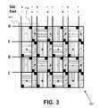
- FIG. 3A first embodiment of an AMLCD panel 300 is shown in FIG. 3 .
- Box 302encloses four TFTs 116 that drive their associated four colored subpixels.
- the gates of each TFT 116are connected to a row line in such a manner as to have same colored subpixels—successively staggered—across each row affect opposite polarity.
- This effectis shown in FIG. 4 , for example, with red subpixels 408 , 410 , and 412 , etc. receiving ( ⁇ , +, ⁇ , . . . ) polarities during a row write to line 404 .
- the same effectis shown for blue subpixels across line 404 .
- any parasitic capacitances(for example, as between the gate and the drain of the TFT, CGD, and as between the pixel and the gate line, CG-Pixel.) that occur across a row/gate line with are minimized by having the same number of “+” and “ ⁇ ” polarities connected to the row/gate line.
- the TFTs 116 in repeating group 302are formed at the intersection of a pair of row and column lines at a given quadrant of the subpixel.
- the upper red subpixel in group 302has its TFT formed in the first quadrant; while the upper green subpixel has its TFT formed in the third quadrant.
- one embodimentis to find a suitable remapping of the TFT backplane from their usual placement in one quadrant, so that the remapping may use any number of quadrants greater than one.
- FIG. 4depicts how panel 300 operates over the course of two successive row-writes.
- row 402sends an active gate signal down to the connected TFTs and their associated subpixels (shown in BOLD hatching) on an EVEN cycle.
- all of the green subpixels in two rowsare activated.
- the TFTshave been advantageously replaced so that two bordering green subpixels in the vertical direction have opposite polarities. So, for example, green subpixel 406 has a “+” polarity; while green subpixel 408 has a “ ⁇ ” polarity.
- the polarities of all of the green subpixels connected to row line 402are balanced—i.e. the number of “+” polarity green subpixels equals the number of “ ⁇ ” polarity green subpixels.
- row line 404sends an active gate signal to its connected TFTs and their associated subpixels (also shown in BOLD hatching) on an ODD cycle. Again, given the replacement of the TFTs, each two adjacent subpixels in the vertical direction have opposite polarity. Additionally, as described above, same colored subpixels that are successively staggered along a row line are of opposite polarity.
- FIG. 5Yet another embodiment comprising a TFT replacement (i.e. off from the traditional manner of consistently placing TFTs in a single position relative to the subpixels —such as the upper left hand corner) is shown in FIG. 5 .
- the repeat grouping of TFTs in this arrangementare shown as block 502 .
- Similar corrective polarity conditions as noted for FIGS. 3 and 4are found with the TFT placement of FIG. 5 .
- every two red subpixelsalternate polarity—e.g. red subpixels 510 and 512 have “+” polarity; while red subpixels 514 and 516 have “ ⁇ ” polarity.
- TFT placementsthere are a number of different TFT placements that will achieve the same effects. Each such TFT placement (or TFT “remapping”) is contemplated within the scope of the present invention and, as such, the present invention should not be limited to any particular TFT placement or remapping.
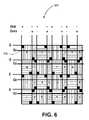
- FIG. 6is yet another embodiment of TFT remapping on panel 600 that may take into account additional parasitic capacitance effects between pixel and the CS electrode 602 .
- two successive row/gate linesare driven by a given polarity scheme (O or E).
- the polarity of each subpixelis shown in its center. It will be noted that along any given row (and hence along a given CS line), successive same colored subpixels alternate polarity.
- FIG. 7Another TFT remapping that may produce similar beneficial effects is shown in FIG. 7 .
- the panel 700is partitioned into sections (e.g. 702 , 704 ) that place the TFTs of their associated subpixels in corners such that the polarity at the two columns at the partition line repeats.
- column 710 and 712have the same polarities of subpixels going down the respective columns.
- the number of subpixels across a row defining a given partitionis small enough, the accumulated parasitic capacitances in that partition may be sufficiently below a visually detectable (or at least manageable) level.
- This partitioning across a panelmight occur a number of times in order to keep those parasitics at a low enough level.
- this panelcould have a 1 ⁇ 2 dot inversion scheme—thereby effectively solving vertical crosstalk (i.e. whereby same colored subpixels have same polarity in a given column).
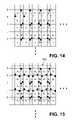
- FIGS. 8 through 15outline a general procedure for developing many different embodiments of TFT remappings that may effect reduced parasitic capacitance in an panel having even modulus for a subpixel repeating group.
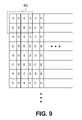
- a repeating subpixel grouping 902is placed upon the grid in FIG. 9 .
- any repeating groupwould suffice here; but preferably one with an even number of subpixels across a row.
- a dot inversion schemeis selected in FIG. 10 —in this case, a 1 ⁇ 2 dot inversion scheme is selected with two polarity schemes or “phases” —O and E. Additionally, these two phases are repeated for every two row/gate lines—O, O, E, E, etc. If 1 ⁇ 1 dot inversion were desired, then the phases would alternate every row/gate line.
- any symmetries in the repeat groupingare now to be considered.
- every other columnis a line of blue subpixels.
- a possible symmetry to consideris in the other columns of alternating red and green subpixels.
- the first two red and green subpixelscould assume a set of four possible polarity values.
- 2N combinations of polaritiesmay or should be considered.
- FIG. 12the polarities in one of the columns of same colored subpixels are considered.
- a listing of possible polaritiesare shown in list 1202 for the second column of blue subpixels—and the first four such blue subpixels in the column are considered.
- the listcould be exhaustive of the possibilities of polarities and certainly another number other than four may be considered.
- One OK combination 1204is selected, solely for exemplary purposes, for grid 1206 .
- FIG. 13shows an initial selection of TFT placements on the grid.
- the polarities accorded to each intersection of a row/gate line and a column/data lineare placed on the grid—as either a “+” or a “ ⁇ ”. It is noted that any TFT placed in any quadrant around an intersection point will effect the same polarity on its associated subpixel.
- the subpixels in FIG. 12 that have been assigned a polaritythere is a degree of freedom in selecting which intersection to place the TFT. For example, red subpixel 1302 has been assigned a “+” polarity and there are two possible intersections 1304 and 1306 at which to place its associated TFT.
- the TFTis selected to be placed at intersection 1304 .
- the placement of TFTscould be affected by many possible factors—for example, the desire to minimally impact design rules, to minimize ill effect (e.g. parasitic capacitances), etc.
- the other TFTs for the polarity-assigned subpixels in FIG. 13have also been placed—as one possible embodiment and selection thereof. Of course, other embodiments/selections are also possible.
- FIG. 14extends this process of TFT placement to the remaining blue subpixels on the grid. Although there are other selections possible, this particular selection was made with the idea of balancing the polarities across any given row. As may be seen, the blue subpixels polarities balance out across any given row/gate line.
- FIG. 15fills in the remaining red and green subpixel TFT placements. One possible goal is to assign the remaining TFTs in a grouping that may be repeated across the entire panel to form the backplane. One such repeat grouping is 1502 in FIG. 15 .
- Grouping 1502is an 8 ⁇ 4 subpixel grouping that seeks to balance polarities across all subpixels in the row and column directions, as well as balancing polarities within each single color subpixel sub-gird in the row and column directions. It will be appreciated that by following the general procedure outlined above and exploiting the various degrees of freedom in design choice, many possible TFT placements or remappings are possible to develop a suitable TFT grid.
- FIG. 16Ashows one possible TFT remapping grid effecting a 1 ⁇ 2 dot inversion scheme.
- FIG. 16Bshows how the remapping grid might be implemented on a panel with a little greater detail.
- TFT 1602 and 1604are possibly susceptible to some uneven effects that might be introduced during the manufacturing process. For example, if the gate metal or pixel electrode masks are translated upwards during manufacturing, then it may be possible for reduced parasitic capacitance for TFT 1602 and its associated pixel and for increased parasitic capacitance for TFT 1604 and its associated pixel. If the errors in parasitics are out of tolerance bounds, then the yield of manufacturing such panels with unconventional TFT remappings might decrease. Thus, it may desirable to redesign the TFT structure as described below in order to abate any uneven effects as noted above.
- FIG. 16Cshows another embodiment of a panel having a novel subpixel repeating group 1650 .
- the patternlooks like:
- FIG. 17Adepicts the “double TFT” arrangement 1700 of the '451 patent.
- Source line 1704connects to the TFT via source electrode 1706 .
- Two gate electrodes 1708are connected to gate line 1702 .
- Two drain electrodes 1710connect to the pixel and are formed such that the two gate electrodes 1708 affect conduction from the source electrode to the drain electrodes when activated. It is noted that there are two crossover regions 1712 that are connected to TFT may produce additional parasitic capacitance between the gate and the source.
- FIGS. 17B and 17Cprovide different alternative embodiments for the double TFT structure to the one shown in FIG. 17A .
- This structurewill enable reduced source to gate capacitance, which can cause crosstalk in certain images.
- the gate to drain crossoverwill be less damaging to image quality.
- One advantage of the embodiment of FIG. 17Cis that there is only one crossover 1732 that may reduce parasitic capacitance.
- FIG. 18depicts a TFT 1800 made in the manner taught in the '297 patent.
- gate line 1802delivers the gate signal to gate electrode 1808 .
- Source line 1804sends image data to source electrodes 1806 .
- the gate electrodeis activated, the image data is transferred to the pixel via the drain electrode 1810 .
- this TFT embodimentcontains only one gate crossover 1812 which aids in reducing parasitic capacitance.
- FIGS. 19 through 21Another set of TFT redesigns are shown in FIGS. 19 through 21 to handle the unevenness of parasitic capacitance that might be introduced by the above described TFT remapping.
- TFTsare remapped on the panel, it is possible for some TFTs on the panel to be implemented in different corners or quadrants of a pixel area. For example, some TFTs may be constructed in the upper left hand corner of the pixel area, some in the upper right hand corner of the pixel area and so on. If all such TFTs were constructed the same way, then it would be likely that the source-drain orientation would be reversed for left hand corner and right hand corner implementation. Such non-uniformity of construction might introduce uneven parasitic capacitance in the case of a given TFT misalignment.
- FIG. 19is one embodiment of a TFT built with a reverse orientation 1902 as compared with a TFT built with a typical orientation 1904 .
- TFT 1904is constructed within the upper left hand corner of its associated pixel in the usual manner—i.e. without any crossovers to avoid any introduced parasitic capacitance. It is noted that the source (S) and drain (D) electrodes are placed in a left-to-right fashion.
- TFT 1902is shown constructed in the upper right hand corner of a pixel area in a reverse orientation—i.e. a crossover 1914 from source line 1906 is constructed so that the source electrode 1910 and drain electrode 1912 are also in left-to-right fashion.
- TFTs 1902 and 1904will receive the same amount of added parasitic capacitance—thus, keeping the panel's defects uniform. It will be appreciated that although TFT 1902 and TFT 1904 are depicted side-by-side and connected to the same column, this is primarily for explanatory purposes. It is unlikely that two adjoining subpixels would share the same column/data line—thus, TFT 1904 and its associated pixel is provided to show the distinction between a normal TFT orientation and TFT 1902 in a reverse orientation.
- FIG. 20shows another embodiment of TFTs 1902 and 1904 .
- a new crossover 2002is added to TFT 1904 so as to balance the added parasitic capacitance via crossover 1914 .
- FIG. 21is yet another embodiment of TFTs 1902 and 1904 .
- the gate electrode crossover 1914has been removed in favor of a gate line crossover 2102 which may have a lesser impact on individual pixel elements.
- FIGS. 22 and 23are embodiments of pixel elements with corners 2210 and 2310 removed to match the one corner removed containing the TFT structure. These pixel elements as designed here may balance the parasitic capacitances more than a normal pixel structure.
- FIG. 24is another embodiment of a pixel structure that employs at least one extra metal line 2410 that may help to shield the pixel element from the parasitic capacitances between the gate lines and the pixel element. Additionally, if a dot inversion scheme is employed, then the opposing polarities on both lines 2410 will also help to balance any parasitic capacitance between the source lines and the pixel elements.
Landscapes
- Physics & Mathematics (AREA)
- Engineering & Computer Science (AREA)
- Nonlinear Science (AREA)
- General Physics & Mathematics (AREA)
- Chemical & Material Sciences (AREA)
- Crystallography & Structural Chemistry (AREA)
- Mathematical Physics (AREA)
- Microelectronics & Electronic Packaging (AREA)
- Optics & Photonics (AREA)
- Computer Hardware Design (AREA)
- Theoretical Computer Science (AREA)
- Control Of Indicators Other Than Cathode Ray Tubes (AREA)
- Liquid Crystal (AREA)
- Liquid Crystal Display Device Control (AREA)
- Devices For Indicating Variable Information By Combining Individual Elements (AREA)
Abstract
Description
This application is a continuation of U.S. patent application Ser. No. 10/456,838, filed on Jun. 6, 2003, and claims the benefit of priority thereof and is now issued as U.S. Pat. No. 7,397,455 which is hereby incorporated by reference.
The present application is related to commonly owned (and filed on even date) United States Patent Applications: (1) United States Patent Publication No. 2004/0246213 (“the '213 application”) U.S. patent application Ser. No. 10/455,925 entitled “DISPLAY PANEL HAVING CROSSOVER CONNECTIONS EFFECTING DOT INVERSION”; (2) U.S. Pat. No. 7,218,301 (“the '301 patent”) U.S. patent application Ser. No. 10/455,931 entitled “SYSTEM AND METHOD OF PERFORMING DOT INVERSION WITH STANDARD DRIVERS AND BACKPLANE ON NOVEL DISPLAY PANEL LAYOUTS”; (3) U.S. Pat. No. 7,209,105 (“the '105 patent”) U.S. patent application Ser. No. 10/455,927 entitled “SYSTEM AND METHOD FOR COMPENSATING FOR VISUAL EFFECTS UPON PANELS HAVING FIXED PATTERN NOISE WITH REDUCED QUANTIZATION ERROR”; (4) U.S. Pat. No. 7,187,353 (“the '353 patent”) U.S. patent application Ser. No. 10/456,806 entitled “DOT INVERSION ON NOVEL DISPLAY PANEL LAYOUTS WITH EXTRA DRIVERS”; and (5) United States Patent Publication No. 2004/0246280 (“the '280 application”) U.S. patent application Ser. No. 10/456,839 entitled “IMAGE DEGRADATION CORRECTION IN NOVEL LIQUID CRYSTAL DISPLAYS,” which are hereby incorporated herein by reference.
In commonly owned United States Patent Applications: (1) U.S. Pat. No. 6,903,754 (“the '754 patent”) U.S. patent application Ser. No. 09/916,232 entitled “ARRANGEMENT OF COLOR PIXELS FOR FULL COLOR IMAGING DEVICES WITH SIMPLIFIED ADDRESSING,” filed Jul. 25, 2001; (2) United States Patent Publication No. 2003/0128225 (“the '225 application”) U.S. patent application Ser. No. 10/278,353 entitled “IMPROVEMENTS TO COLOR FLAT PANEL DISPLAY SUB-PIXEL ARRANGEMENTS AND LAYOUTS FOR SUB-PIXEL RENDERING WITH INCREASED MODULATION TRANSFER FUNCTION RESPONSE,” filed Oct. 22, 2002; (3) United States Patent Publication No. 2003/0128179 (“the '179 application”) U.S. patent application Ser. No. 10/278,352, entitled “IMPROVEMENTS TO COLOR FLAT PANEL DISPLAY SUB-PIXEL ARRANGEMENTS AND LAYOUTS FOR SUB-PIXEL RENDERING WITH SPLIT BLUE SUB-PIXELS,” filed Oct. 22, 2002; (4) United States Patent Publication No. 2004/0051724 (“the '724 application”) U.S. patent application Ser. No. 10/243,094, entitled “IMPROVED FOUR COLOR ARRANGEMENTS AND EMITTERS FOR SUB-PIXEL RENDERING,” filed Sep. 13, 2002; (5) United States Patent Publication No. 2003/0117423 (“the '423 application”) U.S. patent application Ser. No. 10/278,328, entitled “IMPROVEMENTS TO COLOR FLAT PANEL DISPLAY SUB-PIXEL ARRANGEMENTS AND LAYOUTS WITH REDUCED BLUE LUMINANCE WELL VISIBILITY,” filed Oct. 22, 2002; (6) U.S. Pat. No. 7,283,142 (“the '142 patent”) U.S. patent application Ser. No. 10/278,393, entitled “COLOR DISPLAY HAVING HORIZONTAL SUB-PIXEL ARRANGEMENTS AND LAYOUTS,” filed Oct. 22, 2002; (7) United States Patent Publication No. 2004/0080479 (“the '479 application”) U.S. patent application Ser. No. 10/347,001 entitled “IMPROVED SUB-PIXEL ARRANGEMENTS FOR STRIPED DISPLAYS AND METHODS AND SYSTEMS FOR SUB-PIXEL RENDERING SAME,” filed Jan. 16, 2003, novel sub-pixel arrangements are therein disclosed for improving the cost/performance curves for image display devices and herein incorporated by reference.
These improvements are particularly pronounced when coupled with sub-pixel rendering (SPR) systems and methods further disclosed in those applications and in commonly owned United States Patent Applications: (1) U.S. Pat. No. 7,123,277 (“the '277 patent”) U.S. patent application Ser. No. 10/051,612, entitled “CONVERSION OF A SUB-PIXEL FORMAT DATA TO ANOTHER SUB-PIXEL DATA FORMAT,” filed Jan. 16, 2002; (2) U.S. Pat. No. 7,221,381 (“the '381 patent”) U.S. patent application Ser. No. 10/150,355, entitled “METHODS AND SYSTEMS FOR SUB-PIXEL RENDERING WITH GAMMA ADJUSTMENT,” filed May 17, 2002; (3) U.S. Pat. No. 7,184,066 (“the '066 patent”) U.S. patent application Ser. No. 10/215,843, entitled “METHODS AND SYSTEMS FOR SUB-PIXEL RENDERING WITH ADAPTIVE FILTERING,” filed Aug. 8, 2002; (4) United States Patent Publication No. 2004/0196302 (“the '302 application”) U.S. patent application Ser. No. 10/379,767, entitled “SYSTEMS AND METHODS FOR TEMPORAL SUB-PIXEL RENDERING OF IMAGE DATA” filed Mar. 4, 2003; (5) U.S. Pat. No. 7,167,186 (“the '186 patent”) U.S. patent application Ser. No. 10/379,765, entitled “SYSTEMS AND METHODS FOR MOTION ADAPTIVE FILTERING,” filed Mar. 4, 2003; (6) U.S. Pat. No. 6,917,368 (“the '368 patent”) U.S. patent application Ser. No. 10/379,766 entitled “SUB-PIXEL RENDERING SYSTEM AND METHOD FOR IMPROVED DISPLAY VIEWING ANGLES” filed Mar. 4, 2003; (7) U.S. Pat. No. 7,352,374 (“the '374 patent”) U.S. patent application Ser. No. 10/409,413 entitled “IMAGE DATA SET WITH EMBEDDED PRE-SUBPIXEL RENDERED IMAGE” filed Apr. 7, 2003, which are hereby incorporated herein by reference.
The accompanying drawings, which are incorporated in, and constitute a part of this specification illustrate exemplary implementations and embodiments of the invention and, together with the description, serve to explain principles of the invention.
Reference will now be made in detail to implementations and embodiments, examples of which are illustrated in the accompanying drawings. Wherever possible, the same reference numbers will be used throughout the drawings to refer to the same or like parts.
As also shown, each subpixel is connected to a column line (each driven by a column driver110) and a row line (e.g.112 and114). In the field of AMLCD panels, it is known to drive the panel with a dot inversion scheme to reduce crosstalk and flicker.FIG. 1A depicts one particular dot inversion scheme—i.e. 1×1 dot inversion—that is indicated by a “+” and a “−” polarity given in the center of each subpixel. Each row line is typically connected to a gate (not shown inFIG. 1A ) ofTFT 116. Image data—delivered via the column lines—are typically connected to the source of each TFT. Image data is written to the panel a row at a time and is given a polarity bias scheme as indicated herein as either ODD (“O”) or EVEN (“E”) schemes. As shown,row 112 is being written with ODD polarity scheme at a given time whilerow 114 is being written with EVEN polarity scheme at a next time. The polarities alternate ODD and EVEN schemes a row at a time in this 1×1 dot inversion scheme.
In order to affect improved performance, several embodiments are herein described. A first embodiment of anAMLCD panel 300 is shown inFIG. 3 .Box 302 encloses fourTFTs 116 that drive their associated four colored subpixels. As may be seen, the gates of eachTFT 116 are connected to a row line in such a manner as to have same colored subpixels—successively staggered—across each row affect opposite polarity. This effect is shown inFIG. 4 , for example, withred subpixels line 404. The same effect is shown for blue subpixels acrossline 404. One possible benefit of this condition is that any parasitic capacitances (for example, as between the gate and the drain of the TFT, CGD, and as between the pixel and the gate line, CG-Pixel.) that occur across a row/gate line with are minimized by having the same number of “+” and “−” polarities connected to the row/gate line.
It is further seen inFIG. 3 that theTFTs 116 in repeatinggroup 302 are formed at the intersection of a pair of row and column lines at a given quadrant of the subpixel. For example, the upper red subpixel ingroup 302 has its TFT formed in the first quadrant; while the upper green subpixel has its TFT formed in the third quadrant. To affect a dot inversion scheme on a subpixel repeating group of an even number of subpixels in a row or column direction, one embodiment is to find a suitable remapping of the TFT backplane from their usual placement in one quadrant, so that the remapping may use any number of quadrants greater than one.
During the next row-write (as shown inpanel 300 on the right hand side),row line 404 sends an active gate signal to its connected TFTs and their associated subpixels (also shown in BOLD hatching) on an ODD cycle. Again, given the replacement of the TFTs, each two adjacent subpixels in the vertical direction have opposite polarity. Additionally, as described above, same colored subpixels that are successively staggered along a row line are of opposite polarity.
Yet another embodiment comprising a TFT replacement (i.e. off from the traditional manner of consistently placing TFTs in a single position relative to the subpixels —such as the upper left hand corner) is shown inFIG. 5 . The repeat grouping of TFTs in this arrangement are shown asblock 502. With this arrangement, similar corrective polarity conditions as noted forFIGS. 3 and 4 are found with the TFT placement ofFIG. 5 . For example, along row/gate line 504, every two red subpixels alternate polarity—e.g.red subpixels red subpixels
Another TFT remapping that may produce similar beneficial effects is shown inFIG. 7 . In this case, thepanel 700 is partitioned into sections (e.g.702,704) that place the TFTs of their associated subpixels in corners such that the polarity at the two columns at the partition line repeats. Thus, for example,column
Any symmetries in the repeat grouping are now to be considered. For example, inFIG. 11 , it is noted that every other column is a line of blue subpixels. Thus, a possible symmetry to consider is in the other columns of alternating red and green subpixels. Now, consider all possible combinations of polarities for the first two subpixels in the columns of interest. InFIG. 11 for example, the first two red and green subpixels could assume a set of four possible polarity values. In general, if the first N subpixels in relevant rows or columns are considered, then 2N combinations of polarities may or should be considered.
Other symmetries may also be taken into consideration. InFIG. 12 , the polarities in one of the columns of same colored subpixels are considered. A listing of possible polarities are shown inlist 1202 for the second column of blue subpixels—and the first four such blue subpixels in the column are considered. The list could be exhaustive of the possibilities of polarities and certainly another number other than four may be considered. As it may be advantageous to balance the polarities down a given column—all of those possibilities with a balanced number of polarities are noted as “OK”. OneOK combination 1204 is selected, solely for exemplary purposes, forgrid 1206.
- R G B G
- R G B G
- B G R G
- B G R G
When a 1×1 dot inversion scheme is applied to this repeat grouping, vertical crosstalk problems are solved. Additionally, all the TFTs may be place on the same side of the pixel structure—which may reduce some parasitic effects or imbalances.
One known attempt to correct for TFT misalignments and any associated increase in parasitic capacitance is found in U.S. Pat. No. 5,191,451 to Katayama et al.FIG. 17A depicts the “double TFT”arrangement 1700 of the '451 patent. Source line1704 connects to the TFT viasource electrode 1706. Twogate electrodes 1708 are connected togate line 1702. Twodrain electrodes 1710 connect to the pixel and are formed such that the twogate electrodes 1708 affect conduction from the source electrode to the drain electrodes when activated. It is noted that there are twocrossover regions 1712 that are connected to TFT may produce additional parasitic capacitance between the gate and the source. As discussed in the '451 patent, any vertical misalignment of the TFT placement is somewhat corrected by this double TFT arrangement as is discussed therein.FIGS. 17B and 17C provide different alternative embodiments for the double TFT structure to the one shown inFIG. 17A . This structure will enable reduced source to gate capacitance, which can cause crosstalk in certain images. The gate to drain crossover will be less damaging to image quality. One advantage of the embodiment ofFIG. 17C is that there is only onecrossover 1732 that may reduce parasitic capacitance.
Another manner of reducing the ill effects of TFT misalignment is shown in U.S. Pat. No. 5,097,297 to Nakazawa.FIG. 18 depicts aTFT 1800 made in the manner taught in the '297 patent. As may be seen inFIG. 18 ,gate line 1802 delivers the gate signal togate electrode 1808.Source line 1804 sends image data to sourceelectrodes 1806. When the gate electrode is activated, the image data is transferred to the pixel via thedrain electrode 1810. It is noted that this TFT embodiment contains only onegate crossover 1812 which aids in reducing parasitic capacitance.
Another set of TFT redesigns are shown inFIGS. 19 through 21 to handle the unevenness of parasitic capacitance that might be introduced by the above described TFT remapping. As TFTs are remapped on the panel, it is possible for some TFTs on the panel to be implemented in different corners or quadrants of a pixel area. For example, some TFTs may be constructed in the upper left hand corner of the pixel area, some in the upper right hand corner of the pixel area and so on. If all such TFTs were constructed the same way, then it would be likely that the source-drain orientation would be reversed for left hand corner and right hand corner implementation. Such non-uniformity of construction might introduce uneven parasitic capacitance in the case of a given TFT misalignment.
Claims (20)
1. A liquid crystal display comprising:
a display panel substantially comprising a plurality of a subpixel repeating group; the subpixel repeating group comprises at least two rows, each of said rows further comprising an even number of subpixels; wherein each row of subpixels comprises at least two same-colored subpixels;
each said subpixel having an associated thin film transistor (TFT) connected to a row line and a column line; said thin film transistor being formed in a corner of said subpixel in one of a group of quadrants with respect to said subpixel, the group comprising a first quadrant, a second quadrant, a third quadrant and a fourth quadrant;
driver circuitry configured to send image signals and polarity signals to said subpixels; and
wherein said display panel is partitioned into a plurality of sections along a row direction wherein said subpixels in each at a first section have their associated TFTs in a first quadrant and said subpixels in a second section have their TFTs in a second quadrant such that the polarity signal sent to same colored subpixels in said first section are different from polarity signals sent to same colored subpixels in said second section.
2. The liquid crystal display ofclaim 1 wherein said polarity signal comprises a 1×1 dot inversion polarity signal.
3. The liquid crystal display ofclaim 1 wherein said polarity signal comprises a 1×2 dot inversion polarity signal.
4. The liquid crystal display ofclaim 1 wherein the partitioning of said display panel occurs with frequency across said row direction such that parasitic capacitance effects are substantially abated.
5. The liquid crystal display ofclaim 1 , wherein said subpixels in said first section are connected to an odd-numbered column line, and said subpixels in said second section are connected to an even-numbered column line.
6. The liquid crystal display ofclaim 1 , wherein said subpixels in said first section are connected to an even-numbered column line, and said subpixels in said second section are connected to an odd-numbered column line.
7. The liquid crystal display ofclaim 1 , wherein said subpixel repeating group comprises a first subpixel having a first color, a second subpixel having a second color different from the first color, a third color subpixel having a third color different from the first and second colors and a fourth subpixel having the third color in each of said rows.
8. The liquid crystal display ofclaim 7 , wherein the first color is red, the second color is green and the third color is blue.
9. The liquid crystal display ofclaim 7 , wherein the third subpixel has a size smaller than each of the first subpixel and the second subpixel, and the fourth subpixel has a size substantially the same as the third subpixel.
10. The liquid crystal display ofclaim 7 , wherein the first subpixel in a first row and the second subpixel in a second row are disposed in a same column.
11. The liquid crystal display ofclaim 10 , wherein the third subpixel in a first row and the third subpixel in a second row are disposed in a same column.
12. The liquid crystal display ofclaim 11 , wherein the third subpixel of the first row is disposed between the first and second subpixels, and the second subpixel of the first row is disposed between the third and fourth subpixels.
13. The liquid crystal display ofclaim 12 , wherein the first and second subpixels of the first row are connected to a first row line, and the third and fourth subpixels of the first row are connected to a second row line.
14. The liquid crystal display ofclaim 13 , wherein the third and fourth subpixels of the second row are connected to the first row line, and the first and second subpixels of the second row are connected to a third row line.
15. The liquid crystal display ofclaim 12 , wherein the first subpixel of the first row is connected to a first column line, and the second subpixel of the second row, which is disposed in the same column as the first subpixel of the first row, is connected to a second column line.
16. The liquid crystal display ofclaim 15 , wherein the third subpixel of the second row is connected to the second column line, and the third subpixel of the first row, which is disposed in the same column as the third subpixel of the second row, is connected to a third column line.
17. The liquid crystal display ofclaim 12 , wherein the first and third subpixels of the first row are connected to a first row line, and the second and fourth subpixels of the first row are connected to a second row line.
18. The liquid crystal display ofclaim 7 , wherein the first subpixel in a first row and the first subpixel in a second row are disposed in a same column.
19. The liquid crystal display ofclaim 18 , wherein the third subpixel in a first row and the third subpixel in a second row are disposed in a same column.
20. The liquid crystal display ofclaim 19 , wherein the third subpixel of the first row is disposed between the first and second subpixels, and the second subpixel of the first row is disposed between the third and fourth subpixels.
Priority Applications (1)
| Application Number | Priority Date | Filing Date | Title |
|---|---|---|---|
| US12/147,286US8144094B2 (en) | 2003-06-06 | 2008-06-26 | Liquid crystal display backplane layouts and addressing for non-standard subpixel arrangements |
Applications Claiming Priority (2)
| Application Number | Priority Date | Filing Date | Title |
|---|---|---|---|
| US10/456,838US7397455B2 (en) | 2003-06-06 | 2003-06-06 | Liquid crystal display backplane layouts and addressing for non-standard subpixel arrangements |
| US12/147,286US8144094B2 (en) | 2003-06-06 | 2008-06-26 | Liquid crystal display backplane layouts and addressing for non-standard subpixel arrangements |
Related Parent Applications (1)
| Application Number | Title | Priority Date | Filing Date |
|---|---|---|---|
| US10/456,838ContinuationUS7397455B2 (en) | 2003-06-06 | 2003-06-06 | Liquid crystal display backplane layouts and addressing for non-standard subpixel arrangements |
Publications (2)
| Publication Number | Publication Date |
|---|---|
| US20080252581A1 US20080252581A1 (en) | 2008-10-16 |
| US8144094B2true US8144094B2 (en) | 2012-03-27 |
Family
ID=33490247
Family Applications (2)
| Application Number | Title | Priority Date | Filing Date |
|---|---|---|---|
| US10/456,838Expired - LifetimeUS7397455B2 (en) | 2003-06-06 | 2003-06-06 | Liquid crystal display backplane layouts and addressing for non-standard subpixel arrangements |
| US12/147,286Expired - LifetimeUS8144094B2 (en) | 2003-06-06 | 2008-06-26 | Liquid crystal display backplane layouts and addressing for non-standard subpixel arrangements |
Family Applications Before (1)
| Application Number | Title | Priority Date | Filing Date |
|---|---|---|---|
| US10/456,838Expired - LifetimeUS7397455B2 (en) | 2003-06-06 | 2003-06-06 | Liquid crystal display backplane layouts and addressing for non-standard subpixel arrangements |
Country Status (4)
| Country | Link |
|---|---|
| US (2) | US7397455B2 (en) |
| CN (1) | CN1799080B (en) |
| TW (1) | TWI310535B (en) |
| WO (1) | WO2004109635A1 (en) |
Cited By (3)
| Publication number | Priority date | Publication date | Assignee | Title |
|---|---|---|---|---|
| US20160174331A1 (en)* | 2014-12-13 | 2016-06-16 | Vp Assets Limited | Pixel structure |
| CN110456586A (en)* | 2019-08-22 | 2019-11-15 | 京东方科技集团股份有限公司 | Display substrate, display panel and display device |
| US11237445B2 (en) | 2006-09-29 | 2022-02-01 | Semiconductor Energy Laboratory Co., Ltd. | Display device and electronic device |
Families Citing this family (50)
| Publication number | Priority date | Publication date | Assignee | Title |
|---|---|---|---|---|
| US7417648B2 (en)* | 2002-01-07 | 2008-08-26 | Samsung Electronics Co. Ltd., | Color flat panel display sub-pixel arrangements and layouts for sub-pixel rendering with split blue sub-pixels |
| US8035599B2 (en) | 2003-06-06 | 2011-10-11 | Samsung Electronics Co., Ltd. | Display panel having crossover connections effecting dot inversion |
| US20040246280A1 (en) | 2003-06-06 | 2004-12-09 | Credelle Thomas Lloyd | Image degradation correction in novel liquid crystal displays |
| US7187353B2 (en) | 2003-06-06 | 2007-03-06 | Clairvoyante, Inc | Dot inversion on novel display panel layouts with extra drivers |
| US7218301B2 (en) | 2003-06-06 | 2007-05-15 | Clairvoyante, Inc | System and method of performing dot inversion with standard drivers and backplane on novel display panel layouts |
| US7791679B2 (en)* | 2003-06-06 | 2010-09-07 | Samsung Electronics Co., Ltd. | Alternative thin film transistors for liquid crystal displays |
| US7397455B2 (en) | 2003-06-06 | 2008-07-08 | Samsung Electronics Co., Ltd. | Liquid crystal display backplane layouts and addressing for non-standard subpixel arrangements |
| US7209105B2 (en) | 2003-06-06 | 2007-04-24 | Clairvoyante, Inc | System and method for compensating for visual effects upon panels having fixed pattern noise with reduced quantization error |
| KR101039023B1 (en)* | 2004-04-19 | 2011-06-03 | 삼성전자주식회사 | Liquid crystal display |
| KR101100890B1 (en)* | 2005-03-02 | 2012-01-02 | 삼성전자주식회사 | LCD and its driving method |
| US7511716B2 (en) | 2005-04-29 | 2009-03-31 | Sony Corporation | High-resolution micro-lens 3D display with shared sub-pixel color signals |
| TWI343027B (en) | 2005-05-20 | 2011-06-01 | Samsung Electronics Co Ltd | Display systems with multiprimary color subpixel rendering with metameric filtering and method for adjusting image data for rendering onto display as well as method for adjusting intensity values between two sets of colored subpixels on display to minimi |
| KR101189273B1 (en)* | 2005-09-07 | 2012-10-09 | 삼성디스플레이 주식회사 | Driving apparatus for display device and display device including the same |
| KR101182771B1 (en)* | 2005-09-23 | 2012-09-14 | 삼성전자주식회사 | Liquid crystal display panel and method of driving the same and liquid crystal display apparatus using the same |
| EP1770676B1 (en) | 2005-09-30 | 2017-05-03 | Semiconductor Energy Laboratory Co., Ltd. | Display device and electronic device |
| WO2007047537A2 (en) | 2005-10-14 | 2007-04-26 | Clairvoyante, Inc. | Improved gamut mapping and subpixel rendering systems and methods |
| KR20070063169A (en)* | 2005-12-14 | 2007-06-19 | 삼성전자주식회사 | Liquid crystal display |
| US8605017B2 (en) | 2006-06-02 | 2013-12-10 | Samsung Display Co., Ltd. | High dynamic contrast display system having multiple segmented backlight |
| US20080024408A1 (en)* | 2006-07-25 | 2008-01-31 | Tpo Displays Corp. | Systems for displaying images and driving method thereof |
| TWI338804B (en) | 2006-08-14 | 2011-03-11 | Au Optronics Corp | Liquid crystal display sheet |
| US7567370B2 (en)* | 2007-07-26 | 2009-07-28 | Hewlett-Packard Development Company, L.P. | Color display having layer dependent spatial resolution and related method |
| US8295594B2 (en) | 2007-10-09 | 2012-10-23 | Samsung Display Co., Ltd. | Systems and methods for selective handling of out-of-gamut color conversions |
| TWI396912B (en)* | 2008-01-31 | 2013-05-21 | Novatek Microelectronics Corp | Lcd with sub-pixels rearrangement |
| JP2009300748A (en)* | 2008-06-13 | 2009-12-24 | Hitachi Displays Ltd | Display and liquid crystal display |
| TWI393107B (en)* | 2008-07-02 | 2013-04-11 | Au Optronics Corp | Liquid crystal display device |
| KR101252091B1 (en)* | 2008-10-28 | 2013-04-12 | 엘지디스플레이 주식회사 | Liquid crystal display of horizontal electronic fieldapplying type |
| WO2011007613A1 (en)* | 2009-07-17 | 2011-01-20 | シャープ株式会社 | Display device and display device driving method |
| CN102725681B (en) | 2010-01-29 | 2015-01-28 | 夏普株式会社 | Liquid crystal display device |
| TWI407224B (en)* | 2010-07-28 | 2013-09-01 | Au Optronics Corp | Liquid crystal display panel, pixel array substrate and pixel structure thereof |
| FR2971862B1 (en)* | 2011-02-22 | 2016-01-22 | Commissariat Energie Atomique | LIQUID CRYSTAL DISPLAY MATRIX WITH IRREGULAR OPENING GEOMETRY |
| US8797247B2 (en)* | 2011-05-16 | 2014-08-05 | Motorola Solutions, Inc. | Perceived display resolution of a color electronic matrix display |
| CN102231030B (en)* | 2011-07-07 | 2013-04-10 | 南京中电熊猫液晶显示科技有限公司 | Pixel structure of thin film transistor liquid crystal display |
| CN202189199U (en) | 2011-07-27 | 2012-04-11 | 深圳市华星光电技术有限公司 | Liquid crystal display panel |
| CN102903318B (en) | 2011-07-29 | 2015-07-08 | 深圳云英谷科技有限公司 | Display sub-pixel arrangement and its presentation method |
| KR101964766B1 (en) | 2011-08-16 | 2019-04-03 | 삼성디스플레이 주식회사 | Display device and driving method thereof |
| TWI550571B (en) | 2011-11-09 | 2016-09-21 | 友達光電股份有限公司 | Three-dimension display panel and driving method thereof |
| TWI597552B (en)* | 2012-01-20 | 2017-09-01 | 群康科技(深圳)有限公司 | Pixel structures |
| US9165526B2 (en) | 2012-02-28 | 2015-10-20 | Shenzhen Yunyinggu Technology Co., Ltd. | Subpixel arrangements of displays and method for rendering the same |
| KR102005550B1 (en)* | 2012-11-22 | 2019-07-31 | 삼성디스플레이 주식회사 | Organic Light Emitting Display Device |
| CN103969900B (en)* | 2013-01-25 | 2017-07-21 | 乐金显示有限公司 | Liquid crystal display device and driving method thereof |
| KR102127762B1 (en)* | 2013-10-02 | 2020-06-30 | 삼성디스플레이 주식회사 | Flat panel display device |
| KR102263258B1 (en)* | 2014-08-25 | 2021-06-10 | 삼성디스플레이 주식회사 | Organic Light Emitting Display Device and Driving Method Thereof |
| KR20160083325A (en)* | 2014-12-30 | 2016-07-12 | 삼성디스플레이 주식회사 | Display apparatus and method of processing data thereof |
| TWI557719B (en)* | 2015-01-27 | 2016-11-11 | 聯詠科技股份有限公司 | Display panel and display apparatus thereof |
| CN105989787B (en)* | 2015-02-05 | 2019-07-19 | 联咏科技股份有限公司 | display panel and display device thereof |
| CN105185288A (en) | 2015-08-28 | 2015-12-23 | 京东方科技集团股份有限公司 | Pixel array, display driving unit, driving method and display device |
| KR102280009B1 (en)* | 2017-05-24 | 2021-07-21 | 삼성전자주식회사 | Display panel having zig-zag connection structure and display device including the same |
| US10621932B1 (en)* | 2018-10-12 | 2020-04-14 | Novatek Microelectronics Corp. | Sub-pixel rendering data conversion apparatus and method |
| CN110111755A (en)* | 2019-06-18 | 2019-08-09 | 厦门天马微电子有限公司 | A kind of display panel, its driving method and display device |
| CN111653584B (en)* | 2020-06-18 | 2022-08-05 | 厦门天马微电子有限公司 | Display panel, manufacturing method thereof and display device |
Citations (188)
| Publication number | Priority date | Publication date | Assignee | Title |
|---|---|---|---|---|
| US3971065A (en) | 1975-03-05 | 1976-07-20 | Eastman Kodak Company | Color imaging array |
| US4353062A (en) | 1979-05-04 | 1982-10-05 | U.S. Philips Corporation | Modulator circuit for a matrix display device |
| GB2133912A (en) | 1982-12-15 | 1984-08-01 | Citizen Watch Co Ltd | Color display device |
| GB2146478A (en) | 1983-09-08 | 1985-04-17 | Sharp Kk | LCD display devices |
| EP0158366A2 (en) | 1984-04-13 | 1985-10-16 | Sharp Kabushiki Kaisha | Color liquid-crystal display apparatus |
| EP0203005A1 (en) | 1985-05-20 | 1986-11-26 | Roger Menn | Tricolour electroluminescent matrix screen and method for its manufacture |
| US4773737A (en) | 1984-12-17 | 1988-09-27 | Canon Kabushiki Kaisha | Color display panel |
| US4781438A (en) | 1987-01-28 | 1988-11-01 | Nec Corporation | Active-matrix liquid crystal color display panel having a triangular pixel arrangement |
| US4792728A (en) | 1985-06-10 | 1988-12-20 | International Business Machines Corporation | Cathodoluminescent garnet lamp |
| US4800375A (en) | 1986-10-24 | 1989-01-24 | Honeywell Inc. | Four color repetitive sequence matrix array for flat panel displays |
| US4822142A (en) | 1986-12-23 | 1989-04-18 | Hosiden Electronics Co. Ltd. | Planar display device |
| EP0322106A2 (en) | 1987-11-28 | 1989-06-28 | THORN EMI plc | Display device |
| US4853592A (en) | 1988-03-10 | 1989-08-01 | Rockwell International Corporation | Flat panel display having pixel spacing and luminance levels providing high resolution |
| US4886343A (en) | 1988-06-20 | 1989-12-12 | Honeywell Inc. | Apparatus and method for additive/subtractive pixel arrangement in color mosaic displays |
| US4908609A (en) | 1986-04-25 | 1990-03-13 | U.S. Philips Corporation | Color display device |
| US4920409A (en) | 1987-06-23 | 1990-04-24 | Casio Computer Co., Ltd. | Matrix type color liquid crystal display device |
| US4965565A (en) | 1987-05-06 | 1990-10-23 | Nec Corporation | Liquid crystal display panel having a thin-film transistor array for displaying a high quality picture |
| US5006840A (en) | 1984-04-13 | 1991-04-09 | Sharp Kabushiki Kaisha | Color liquid-crystal display apparatus with rectilinear arrangement |
| US5052785A (en) | 1989-07-07 | 1991-10-01 | Fuji Photo Film Co., Ltd. | Color liquid crystal shutter having more green electrodes than red or blue electrodes |
| US5083853A (en) | 1987-11-18 | 1992-01-28 | International Business Machines Corporation | Color liquid crystal display device having light-shielding conductive layers |
| US5097297A (en) | 1988-03-18 | 1992-03-17 | Seiko Epson Corporation | Thin film transistor |
| US5113274A (en) | 1988-06-13 | 1992-05-12 | Mitsubishi Denki Kabushiki Kaisha | Matrix-type color liquid crystal display device |
| US5124695A (en) | 1986-09-20 | 1992-06-23 | Thorn Emi Plc | Display device |
| US5184114A (en) | 1982-11-04 | 1993-02-02 | Integrated Systems Engineering, Inc. | Solid state color display system and light emitting diode pixels therefor |
| US5191451A (en) | 1990-04-20 | 1993-03-02 | Sharp Kabushiki Kaisha | Active matrix display device having drain electrodes of the pair of tfts being symmetrically formed with respect to the central plane to prevent the flicker due to the different parasitic capacitances |
| US5311337A (en) | 1992-09-23 | 1994-05-10 | Honeywell Inc. | Color mosaic matrix display having expanded or reduced hexagonal dot pattern |
| US5315418A (en) | 1992-06-17 | 1994-05-24 | Xerox Corporation | Two path liquid crystal light valve color display with light coupling lens array disposed along the red-green light path |
| US5334996A (en) | 1989-12-28 | 1994-08-02 | U.S. Philips Corporation | Color display apparatus |
| US5341153A (en) | 1988-06-13 | 1994-08-23 | International Business Machines Corporation | Method of and apparatus for displaying a multicolor image |
| US5384266A (en) | 1992-12-11 | 1995-01-24 | U.S. Philips Corporation | Electronic device manufacture using ion implantation |
| US5398066A (en) | 1993-07-27 | 1995-03-14 | Sri International | Method and apparatus for compression and decompression of digital color images |
| US5436747A (en) | 1990-08-16 | 1995-07-25 | International Business Machines Corporation | Reduced flicker liquid crystal display |
| EP0671650A2 (en) | 1994-03-11 | 1995-09-13 | Canon Information Systems Research Australia Pty Ltd. | A luminance weighted discrete level display |
| US5459595A (en) | 1992-02-07 | 1995-10-17 | Sharp Kabushiki Kaisha | Active matrix liquid crystal display |
| US5461503A (en) | 1993-04-08 | 1995-10-24 | Societe D'applications Generales D'electricite Et De Mecanique Sagem | Color matrix display unit with double pixel area for red and blue pixels |
| US5485293A (en) | 1993-09-29 | 1996-01-16 | Honeywell Inc. | Liquid crystal display including color triads with split pixels |
| US5535028A (en) | 1993-04-03 | 1996-07-09 | Samsung Electronics Co., Ltd. | Liquid crystal display panel having nonrectilinear data lines |
| US5563621A (en) | 1991-11-18 | 1996-10-08 | Black Box Vision Limited | Display apparatus |
| US5579027A (en) | 1992-01-31 | 1996-11-26 | Canon Kabushiki Kaisha | Method of driving image display apparatus |
| US5646702A (en) | 1994-10-31 | 1997-07-08 | Honeywell Inc. | Field emitter liquid crystal display |
| US5648793A (en) | 1992-01-08 | 1997-07-15 | Industrial Technology Research Institute | Driving system for active matrix liquid crystal display |
| EP0812114A1 (en) | 1995-12-21 | 1997-12-10 | Sony Corporation | Solid-state image sensor, method for driving the same, and solid-state camera device and camera system |
| US5739802A (en) | 1995-05-24 | 1998-04-14 | Rockwell International | Staged active matrix liquid crystal display with separated backplane conductors and method of using the same |
| US5754163A (en) | 1994-08-26 | 1998-05-19 | Lg Electronics Inc. | Liquid crystal display controlling apparatus |
| US5754226A (en) | 1994-12-20 | 1998-05-19 | Sharp Kabushiki Kaisha | Imaging apparatus for obtaining a high resolution image |
| US5767829A (en) | 1994-08-23 | 1998-06-16 | U.S. Philips Corporation | Liquid crystal display device including drive circuit for predetermining polarization state |
| US5808594A (en) | 1994-09-26 | 1998-09-15 | Canon Kabushiki Kaisha | Driving method for display device and display apparatus |
| US5818405A (en) | 1995-11-15 | 1998-10-06 | Cirrus Logic, Inc. | Method and apparatus for reducing flicker in shaded displays |
| US5818968A (en) | 1995-03-20 | 1998-10-06 | Sony Corporation | High-efficiency coding method, high-efficiency coding apparatus, recording and reproducing apparatus, and information transmission system |
| US5877512A (en) | 1995-07-28 | 1999-03-02 | Samsung Electronics Co., Ltd. | Liquid crystal display device having uniform parasitic capacitance between pixels |
| EP0899604A2 (en) | 1997-08-28 | 1999-03-03 | Canon Kabushiki Kaisha | Color display apparatus |
| DE19746329A1 (en) | 1997-09-13 | 1999-03-18 | Gia Chuong Dipl Ing Phan | Display device for e.g. video |
| US5899550A (en) | 1996-08-26 | 1999-05-04 | Canon Kabushiki Kaisha | Display device having different arrangements of larger and smaller sub-color pixels |
| US5949396A (en) | 1996-12-28 | 1999-09-07 | Lg Semicon Co., Ltd. | Thin film transistor-liquid crystal display |
| DE29909537U1 (en) | 1999-05-31 | 1999-09-09 | Phan, Gia Chuong, Hongkong | Display and its control |
| US5971546A (en) | 1996-06-15 | 1999-10-26 | Lg Electronics Inc. | Image display device |
| US6002446A (en) | 1997-02-24 | 1999-12-14 | Paradise Electronics, Inc. | Method and apparatus for upscaling an image |
| US6005692A (en) | 1997-05-29 | 1999-12-21 | Stahl; Thomas D. | Light-emitting diode constructions |
| US6023315A (en) | 1995-07-04 | 2000-02-08 | Sharp Kabushiki Kaisha | Spatial light modulator and directional display |
| US6037719A (en) | 1998-04-09 | 2000-03-14 | Hughes Electronics Corporation | Matrix-addressed display having micromachined electromechanical switches |
| US6064363A (en) | 1997-04-07 | 2000-05-16 | Lg Semicon Co., Ltd. | Driving circuit and method thereof for a display device |
| US6069670A (en) | 1995-05-02 | 2000-05-30 | Innovision Limited | Motion compensated filtering |
| US6088050A (en) | 1996-12-31 | 2000-07-11 | Eastman Kodak Company | Non-impact recording apparatus operable under variable recording conditions |
| EP0878969A3 (en) | 1997-05-15 | 2000-07-19 | Matsushita Electric Industrial Co., Ltd. | LED display device and method for controlling the same |
| US6097367A (en) | 1996-09-06 | 2000-08-01 | Matsushita Electric Industrial Co., Ltd. | Display device |
| US6108122A (en) | 1998-04-29 | 2000-08-22 | Sharp Kabushiki Kaisha | Light modulating devices |
| US6115092A (en) | 1999-09-15 | 2000-09-05 | Rainbow Displays, Inc. | Compensation for edge effects and cell gap variation in tiled flat-panel, liquid crystal displays |
| US6147664A (en) | 1997-08-29 | 2000-11-14 | Candescent Technologies Corporation | Controlling the brightness of an FED device using PWM on the row side and AM on the column side |
| US6151001A (en) | 1998-01-30 | 2000-11-21 | Electro Plasma, Inc. | Method and apparatus for minimizing false image artifacts in a digitally controlled display monitor |
| DE19923527A1 (en) | 1999-05-21 | 2000-11-23 | Leurocom Visuelle Informations | Display device for characters and symbols using matrix of light emitters, excites emitters of mono colors in multiplex phases |
| US6160535A (en) | 1997-06-16 | 2000-12-12 | Samsung Electronics Co., Ltd. | Liquid crystal display devices capable of improved dot-inversion driving and methods of operation thereof |
| WO2001010112A2 (en) | 1999-07-30 | 2001-02-08 | Microsoft Corporation | Methods and apparatus for filtering and caching data representing images |
| US6188385B1 (en) | 1998-10-07 | 2001-02-13 | Microsoft Corporation | Method and apparatus for displaying images such as text |
| US6219019B1 (en) | 1996-09-05 | 2001-04-17 | Kabushiki Kaisha Toshiba | Liquid crystal display apparatus and method for driving the same |
| US6225973B1 (en) | 1998-10-07 | 2001-05-01 | Microsoft Corporation | Mapping samples of foreground/background color image data to pixel sub-components |
| US6225967B1 (en) | 1996-06-19 | 2001-05-01 | Alps Electric Co., Ltd. | Matrix-driven display apparatus and a method for driving the same |
| US6236390B1 (en) | 1998-10-07 | 2001-05-22 | Microsoft Corporation | Methods and apparatus for positioning displayed characters |
| US6243070B1 (en) | 1998-10-07 | 2001-06-05 | Microsoft Corporation | Method and apparatus for detecting and reducing color artifacts in images |
| US6243055B1 (en) | 1994-10-25 | 2001-06-05 | James L. Fergason | Optical display system and method with optical shifting of pixel position including conversion of pixel layout to form delta to stripe pattern by time base multiplexing |
| WO2001052546A2 (en) | 2000-01-10 | 2001-07-19 | Koninklijke Philips Electronics N.V. | Image interpolation and decimation using a continuously variable delay filter and combined with a polyphase filter |
| DE20109354U1 (en) | 2000-06-27 | 2001-08-09 | Giantplus Technology Co., Ltd., Toufen Chen, Miaoli | Color flat screen with two-color filter |
| US20010015716A1 (en) | 1997-09-30 | 2001-08-23 | Dong-Gyu Kim | Liquid crystal display and a method for driving the same |
| US20010017607A1 (en) | 1999-12-31 | 2001-08-30 | Kwon Keuk-Sang | Liquid crystal display device having quad type color filters |
| US6327008B1 (en) | 1995-12-12 | 2001-12-04 | Lg Philips Co. Ltd. | Color liquid crystal display unit |
| US20010048764A1 (en) | 1999-01-12 | 2001-12-06 | Claude Betrisey | Methods apparatus and data structures for enhancing the resolution of images to be rendered on patterned display devices |
| US6332030B1 (en) | 1998-01-15 | 2001-12-18 | The Regents Of The University Of California | Method for embedding and extracting digital data in images and video |
| US20010052897A1 (en) | 2000-06-19 | 2001-12-20 | Taketoshi Nakano | Column electrode driving circuit for use with image display device and image display device incorporating the same |
| US6335719B1 (en) | 1998-07-04 | 2002-01-01 | Lg. Philips Lcd Co., Ltd. | Method and apparatus for driving liquid crystal panel in dot inversion |
| US6340998B1 (en) | 1998-05-20 | 2002-01-22 | Samsung Display Devices Co., Ltd | Thin film transistor liquid crystal display including at least three transistors associated with an unit pixel |
| US6342876B1 (en) | 1998-10-21 | 2002-01-29 | Lg. Phillips Lcd Co., Ltd | Method and apparatus for driving liquid crystal panel in cycle inversion |
| US20020015110A1 (en) | 2000-07-28 | 2002-02-07 | Clairvoyante Laboratories, Inc. | Arrangement of color pixels for full color imaging devices with simplified addressing |
| US6348929B1 (en) | 1998-01-16 | 2002-02-19 | Intel Corporation | Scaling algorithm and architecture for integer scaling in video |
| US20020030780A1 (en) | 1996-10-29 | 2002-03-14 | Shinichi Nishida | Active matrix liquid crystal display panel |
| US6377262B1 (en) | 1999-07-30 | 2002-04-23 | Microsoft Corporation | Rendering sub-pixel precision characters having widths compatible with pixel precision characters |
| US6388644B1 (en) | 1999-02-24 | 2002-05-14 | U.S. Philips Corporation | Color display device |
| US6392717B1 (en) | 1997-05-30 | 2002-05-21 | Texas Instruments Incorporated | High brightness digital display system |
| US6396505B1 (en) | 1998-10-07 | 2002-05-28 | Microsoft Corporation | Methods and apparatus for detecting and reducing color errors in images |
| WO2002059685A2 (en) | 2001-01-26 | 2002-08-01 | International Business Machines Corporation | Adjusting subpixel intensity values based upon luminance characteristics of the subpixels in liquid crystal displays |
| TW499664B (en) | 2000-10-31 | 2002-08-21 | Au Optronics Corp | Drive circuit of liquid crystal display panel and liquid crystal display |
| US6469756B1 (en) | 2000-11-17 | 2002-10-22 | Intel Corporation | Compensating for aperture parallax distortion in tiled displays |
| US6469766B2 (en) | 2000-12-18 | 2002-10-22 | Three-Five Systems, Inc. | Reconfigurable microdisplay |
| US20020158997A1 (en) | 1999-12-24 | 2002-10-31 | Tetsuo Fukami | Liquid crystal device |
| EP1261014A2 (en) | 2001-05-12 | 2002-11-27 | Philips Corporate Intellectual Property GmbH | Plasma display panel with pixel-forming matrix-array |
| WO2002099557A2 (en) | 2001-06-07 | 2002-12-12 | Genoa Technologies Ltd. | System and method of data conversion for wide gamut displays |
| WO2002101644A2 (en) | 2001-06-11 | 2002-12-19 | Genoa Technologies Ltd. | Device, system and method for color display |
| US20030006978A1 (en) | 2001-07-09 | 2003-01-09 | Tatsumi Fujiyoshi | Image-signal driving circuit eliminating the need to change order of inputting image data to source driver |
| US20030011603A1 (en) | 2001-06-20 | 2003-01-16 | Noriyuki Koyama | Character display apparatus, character display method, character display program, and recording medium therefor |
| US20030016310A1 (en) | 2001-07-11 | 2003-01-23 | Lee Joun Ho | Liquid crystal display device |
| US20030034992A1 (en) | 2001-05-09 | 2003-02-20 | Clairvoyante Laboratories, Inc. | Conversion of a sub-pixel format data to another sub-pixel data format |
| WO2003014819A1 (en) | 2001-08-07 | 2003-02-20 | Samsung Electronics Co., Ltd. | A liquid crystal display |
| US6545653B1 (en) | 1994-07-14 | 2003-04-08 | Matsushita Electric Industrial Co., Ltd. | Method and device for displaying image signals and viewfinder |
| US20030071943A1 (en) | 2001-10-12 | 2003-04-17 | Lg.Philips Lcd., Ltd. | Data wire device of pentile matrix display device |
| US6552706B1 (en) | 1999-07-21 | 2003-04-22 | Nec Corporation | Active matrix type liquid crystal display apparatus |
| WO2003034380A2 (en) | 2001-10-19 | 2003-04-24 | Koninklijke Philips Electronics N.V. | Method of and display processing unit for displaying a colour image and a display apparatus comprising such a display processing unit |
| US20030077000A1 (en) | 2001-10-18 | 2003-04-24 | Microsoft Corporation | Generating resized images using ripple free image filtering |
| US20030090581A1 (en) | 2000-07-28 | 2003-05-15 | Credelle Thomas Lloyd | Color display having horizontal sub-pixel arrangements and layouts |
| US6570584B1 (en) | 2000-05-15 | 2003-05-27 | Eastman Kodak Company | Broad color gamut display |
| WO2003050605A1 (en) | 2001-11-23 | 2003-06-19 | Samsung Electronics Co., Ltd. | A thin film transistor array for a liquid crystal display |
| US20030117423A1 (en) | 2001-12-14 | 2003-06-26 | Brown Elliott Candice Hellen | Color flat panel display sub-pixel arrangements and layouts with reduced blue luminance well visibility |
| US20030128179A1 (en) | 2002-01-07 | 2003-07-10 | Credelle Thomas Lloyd | Color flat panel display sub-pixel arrangements and layouts for sub-pixel rendering with split blue sub-pixels |
| WO2003056383A1 (en) | 2001-12-24 | 2003-07-10 | Samsung Electronics Co., Ltd. | A liquid crystal display |
| US20030128225A1 (en) | 2002-01-07 | 2003-07-10 | Credelle Thomas Lloyd | Color flat panel display sub-pixel arrangements and layouts for sub-pixel rendering with increased modulation transfer function response |
| US20030146893A1 (en) | 2002-01-30 | 2003-08-07 | Daiichi Sawabe | Liquid crystal display device |
| US6624828B1 (en) | 1999-02-01 | 2003-09-23 | Microsoft Corporation | Method and apparatus for improving the quality of displayed images through the use of user reference information |
| US20030189537A1 (en) | 2002-04-08 | 2003-10-09 | Yun Sang Chang | Liquid crystal display and driving method thereof |
| US20030214499A1 (en) | 1999-05-26 | 2003-11-20 | Olympus Optical Co., Ltd. | Color reproduction system for making color display of four or more primary colors based on input tristimulus values |
| US20030218618A1 (en) | 1997-09-13 | 2003-11-27 | Phan Gia Chuong | Dynamic pixel resolution, brightness and contrast for displays using spatial elements |
| US6674430B1 (en) | 1998-07-16 | 2004-01-06 | The Research Foundation Of State University Of New York | Apparatus and method for real-time volume processing and universal 3D rendering |
| JP2004004822A (en) | 2002-05-04 | 2004-01-08 | Samsung Electronics Co Ltd | Four-color drive liquid crystal display device and display panel used therefor (LIQUID CRYSTALD DISPLAY SUSING 4 COLORAND PANEL FOR THE SAME) |
| EP1381020A2 (en) | 1999-04-28 | 2004-01-14 | Barco N.V. | Method for displaying images on a display device, as well as a display device used therefor |
| US20040008208A1 (en) | 1999-02-01 | 2004-01-15 | Bodin Dresevic | Quality of displayed images with user preference information |
| US6680761B1 (en) | 2000-01-24 | 2004-01-20 | Rainbow Displays, Inc. | Tiled flat-panel display having visually imperceptible seams, optimized for HDTV applications |
| WO2004017129A1 (en) | 2002-08-14 | 2004-02-26 | Samsung Electronics Co., Ltd. | Pixel array for display device and liquid crystal display |
| WO2004021323A2 (en) | 2002-08-30 | 2004-03-11 | Samsung Electronics Co., Ltd. | Liquid crystal display and driving method thereof |
| JP2004078218A (en) | 2002-08-14 | 2004-03-11 | Samsung Electronics Co Ltd | Liquid crystal display |
| US20040046714A1 (en) | 2001-05-09 | 2004-03-11 | Clairvoyante Laboratories, Inc. | Color flat panel display sub-pixel arrangements and layouts |
| US6714212B1 (en) | 1993-10-05 | 2004-03-30 | Canon Kabushiki Kaisha | Display apparatus |
| US6714206B1 (en) | 2001-12-10 | 2004-03-30 | Silicon Image | Method and system for spatial-temporal dithering for displays with overlapping pixels |
| US6714243B1 (en) | 1999-03-22 | 2004-03-30 | Biomorphic Vlsi, Inc. | Color filter pattern |
| US20040061710A1 (en) | 2000-06-12 | 2004-04-01 | Dean Messing | System for improving display resolution |
| WO2004027503A1 (en) | 2002-09-18 | 2004-04-01 | Samsung Electronics Co., Ltd. | Liquid crystal display |
| US20040075764A1 (en) | 2002-10-18 | 2004-04-22 | Patrick Law | Method and system for converting interlaced formatted video to progressive scan video using a color edge detection scheme |
| US6727878B2 (en) | 2000-02-04 | 2004-04-27 | Nec Lcd Technologies, Ltd. | Liquid crystal display |
| US6738204B1 (en) | 2003-05-16 | 2004-05-18 | Toppoly Optoelectronics Corp. | Arrangement of color elements for a color filter |
| US20040094766A1 (en) | 2002-11-14 | 2004-05-20 | Samsung Electronics Co., Ltd. | Liquid crystal display and thin film transistor array panel therefor |
| US20040095521A1 (en) | 2002-11-20 | 2004-05-20 | Keun-Kyu Song | Four color liquid crystal display and panel therefor |
| US20040104873A1 (en) | 2002-12-03 | 2004-06-03 | Lg.Philips Co., Ltd. | Apparatus and method data-driving for liquid crystal display device |
| US20040108818A1 (en) | 2002-12-10 | 2004-06-10 | Eastman Kodak Company | Color OLED display having repeated patterns of colored light emitting elements |
| US6750875B1 (en) | 1999-02-01 | 2004-06-15 | Microsoft Corporation | Compression of image data associated with two-dimensional arrays of pixel sub-components |
| US20040114046A1 (en) | 2002-12-17 | 2004-06-17 | Samsung Electronics Co., Ltd. | Method and apparatus for rendering image signal |
| US20040140983A1 (en) | 2003-01-22 | 2004-07-22 | Credelle Thomas Lloyd | System and methods of subpixel rendering implemented on display panels |
| US6771028B1 (en) | 2003-04-30 | 2004-08-03 | Eastman Kodak Company | Drive circuitry for four-color organic light-emitting device |
| US20040150651A1 (en) | 1997-09-13 | 2004-08-05 | Phan Gia Chuong | Dynamic pixel resolution, brightness and contrast for displays using spatial elements |
| US20040155895A1 (en) | 2003-02-06 | 2004-08-12 | Chih-Chang Lai | Method and apparatus for imrpoving resolution of display unit |
| US20040179160A1 (en) | 2003-03-13 | 2004-09-16 | Samsung Electronics Co., Ltd. | Four color liquid crystal display and panel therefor |
| US20040189664A1 (en) | 2003-03-25 | 2004-09-30 | Frisken Sarah F. | Method for antialiasing a set of objects represented as a set of two-dimensional distance fields in object-order |
| US20040189662A1 (en) | 2003-03-25 | 2004-09-30 | Frisken Sarah F. | Method for antialiasing an object represented as a two-dimensional distance field in object-order |
| WO2004086128A1 (en) | 2003-03-24 | 2004-10-07 | Samsung Electronics Co., Ltd. | Four color liquid crystal display |
| US6804407B2 (en) | 2000-02-04 | 2004-10-12 | Eastman Kodak Company | Method of image processing |
| US20040213449A1 (en) | 2003-02-03 | 2004-10-28 | Photon Dynamics, Inc. | Method and apparatus for optical inspection of a display |
| US20040223005A1 (en) | 2003-03-25 | 2004-11-11 | Lee Baek-Woon | Apparatus and method of driving display device |
| US20040246404A1 (en)* | 2003-06-06 | 2004-12-09 | Elliott Candice Hellen Brown | Liquid crystal display backplane layouts and addressing for non-standard subpixel arrangements |
| US20040246279A1 (en) | 2003-06-06 | 2004-12-09 | Credelle Thomas Lloyd | Dot inversion on novel display panel layouts with extra drivers |
| US20040246278A1 (en) | 2003-06-06 | 2004-12-09 | Elliott Candice Hellen Brown | System and method for compensating for visual effects upon panels having fixed pattern noise with reduced quantization error |
| US20040247070A1 (en) | 1997-11-26 | 2004-12-09 | Fazle Ali | Computed tomography fluoroscopy system |
| US20040246381A1 (en) | 2003-06-06 | 2004-12-09 | Credelle Thomas Lloyd | System and method of performing dot inversion with standard drivers and backplane on novel display panel layouts |
| US20040246213A1 (en) | 2003-06-06 | 2004-12-09 | Credelle Thomas Lloyd | Display panel having crossover connections effecting dot inversion |
| US20040246280A1 (en) | 2003-06-06 | 2004-12-09 | Credelle Thomas Lloyd | Image degradation correction in novel liquid crystal displays |
| US20040263528A1 (en) | 2003-06-26 | 2004-12-30 | Murdoch Michael J. | Method for transforming three color input signals to four or more output signals for a color display |
| US20050007539A1 (en) | 2003-05-15 | 2005-01-13 | Satoshi Taguchi | Electro-optical device, electronic apparatus, and method of manufacturing the electro-optical device |
| US20050024380A1 (en) | 2003-07-28 | 2005-02-03 | Lin Lin | Method for reducing random access memory of IC in display devices |
| US20050040760A1 (en) | 2003-05-15 | 2005-02-24 | Satoshi Taguchi | Electro-optical device and electronic apparatus device |
| US20050068477A1 (en) | 2003-09-25 | 2005-03-31 | Kyoung-Ju Shin | Liquid crystal display |
| US20050083356A1 (en) | 2003-10-16 | 2005-04-21 | Nam-Seok Roh | Display device and driving method thereof |
| US6885380B1 (en) | 2003-11-07 | 2005-04-26 | Eastman Kodak Company | Method for transforming three colors input signals to four or more output signals for a color display |
| WO2005050296A1 (en) | 2003-11-20 | 2005-06-02 | Samsung Electronics Co., Ltd. | Apparatus and method of converting image signal for six color display device, and six color display device having optimum subpixel arrangement |
| US6903378B2 (en) | 2003-06-26 | 2005-06-07 | Eastman Kodak Company | Stacked OLED display having improved efficiency |
| US20050140634A1 (en) | 2003-12-26 | 2005-06-30 | Nec Corporation | Liquid crystal display device, and method and circuit for driving liquid crystal display device |
| US20050151752A1 (en) | 1997-09-13 | 2005-07-14 | Vp Assets Limited | Display and weighted dot rendering method |
| US6930676B2 (en) | 2001-06-18 | 2005-08-16 | Koninklijke Philips Electronics N.V. | Anti motion blur display |
| US6937217B2 (en) | 2001-03-27 | 2005-08-30 | Koninklijke Philips Electronics N.V. | Display device and method of displaying an image |
| US20050219274A1 (en) | 2003-12-30 | 2005-10-06 | Samsung Electronics Co., Ltd. | Apparatus and method of converting image signal for four-color display device, and display device including the same |
| US6995346B2 (en) | 2002-12-11 | 2006-02-07 | Dialog Semiconductor Gmbh | Fixed pattern noise compensation with low memory requirements |
| US7129955B2 (en) | 2001-10-23 | 2006-10-31 | Matsushita Electric Industrial Co., Ltd. | Image displaying method and image displaying device |
| US7151518B2 (en) | 2001-09-13 | 2006-12-19 | Hitachi, Ltd. | Liquid crystal display device and driving method of the same |
| US20070229430A1 (en)* | 2006-03-31 | 2007-10-04 | Wintek Corporation | Multi-domain liquid crystal display |
| US20090051638A1 (en)* | 2006-02-02 | 2009-02-26 | Sharp Kabushiki Kaisha | Display device |
| US20090102769A1 (en)* | 2007-10-23 | 2009-04-23 | Nec Lcd Technologies, Ltd. | Image display device, and image display method used for same |
Family Cites Families (14)
| Publication number | Priority date | Publication date | Assignee | Title |
|---|---|---|---|---|
| US557A (en)* | 1838-01-09 | James macgregor | ||
| JPS606685A (en) | 1983-06-24 | 1985-01-14 | Otsuka Pharmaceut Co Ltd | Carbostyril derivative |
| JPS60107022U (en) | 1983-12-23 | 1985-07-20 | 太平洋セメント株式会社 | belt cleaner |
| JPH06102503B2 (en) | 1985-12-24 | 1994-12-14 | 古河電気工業株式会社 | Adhesive tape sticking device |
| JPH0467091A (en)* | 1990-07-09 | 1992-03-03 | Internatl Business Mach Corp <Ibm> | Liquid crystal display unit |
| US5481275A (en)* | 1992-11-02 | 1996-01-02 | The 3Do Company | Resolution enhancement for video display using multi-line interpolation |
| JPH06324649A (en) | 1993-05-14 | 1994-11-25 | Sony Corp | Solid-state display device |
| JPH08202317A (en) | 1995-01-31 | 1996-08-09 | Mitsubishi Electric Corp | Liquid crystal display device and driving method thereof |
| US5874986A (en)* | 1996-06-26 | 1999-02-23 | At&T Corp | Method for communicating audiovisual programs over a communications network |
| JPH1068931A (en) | 1996-08-28 | 1998-03-10 | Sharp Corp | Active matrix type liquid crystal display |
| JP3504496B2 (en)* | 1998-05-11 | 2004-03-08 | アルプス電気株式会社 | Driving method and driving circuit for liquid crystal display device |
| JP2001228457A (en) | 1999-12-08 | 2001-08-24 | Sharp Corp | Liquid crystal display |
| JP3596677B2 (en)* | 2000-10-06 | 2004-12-02 | セイコーエプソン株式会社 | Image processing apparatus, image processing method, program, and recording medium |
| US7102605B2 (en)* | 2002-09-30 | 2006-09-05 | Nanosys, Inc. | Integrated displays using nanowire transistors |
- 2003
- 2003-06-06USUS10/456,838patent/US7397455B2/ennot_activeExpired - Lifetime
- 2004
- 2004-06-04WOPCT/US2004/017796patent/WO2004109635A1/enactiveApplication Filing
- 2004-06-04CNCN2004800149970Apatent/CN1799080B/ennot_activeExpired - Lifetime
- 2004-06-04TWTW093116110Apatent/TWI310535B/ennot_activeIP Right Cessation
- 2008
- 2008-06-26USUS12/147,286patent/US8144094B2/ennot_activeExpired - Lifetime
Patent Citations (229)
| Publication number | Priority date | Publication date | Assignee | Title |
|---|---|---|---|---|
| US3971065A (en) | 1975-03-05 | 1976-07-20 | Eastman Kodak Company | Color imaging array |
| US4353062A (en) | 1979-05-04 | 1982-10-05 | U.S. Philips Corporation | Modulator circuit for a matrix display device |
| US5184114A (en) | 1982-11-04 | 1993-02-02 | Integrated Systems Engineering, Inc. | Solid state color display system and light emitting diode pixels therefor |
| GB2133912A (en) | 1982-12-15 | 1984-08-01 | Citizen Watch Co Ltd | Color display device |
| US4642619A (en) | 1982-12-15 | 1987-02-10 | Citizen Watch Co., Ltd. | Non-light-emitting liquid crystal color display device |
| GB2146478A (en) | 1983-09-08 | 1985-04-17 | Sharp Kk | LCD display devices |
| US4651148A (en) | 1983-09-08 | 1987-03-17 | Sharp Kabushiki Kaisha | Liquid crystal display driving with switching transistors |
| EP0158366A2 (en) | 1984-04-13 | 1985-10-16 | Sharp Kabushiki Kaisha | Color liquid-crystal display apparatus |
| US5006840A (en) | 1984-04-13 | 1991-04-09 | Sharp Kabushiki Kaisha | Color liquid-crystal display apparatus with rectilinear arrangement |
| US5144288A (en) | 1984-04-13 | 1992-09-01 | Sharp Kabushiki Kaisha | Color liquid-crystal display apparatus using delta configuration of picture elements |
| US5311205A (en) | 1984-04-13 | 1994-05-10 | Sharp Kabushiki Kaisha | Color liquid-crystal display apparatus with rectilinear arrangement |
| US4773737A (en) | 1984-12-17 | 1988-09-27 | Canon Kabushiki Kaisha | Color display panel |
| US4874986A (en) | 1985-05-20 | 1989-10-17 | Roger Menn | Trichromatic electroluminescent matrix screen, and method of manufacture |
| EP0203005A1 (en) | 1985-05-20 | 1986-11-26 | Roger Menn | Tricolour electroluminescent matrix screen and method for its manufacture |
| US4792728A (en) | 1985-06-10 | 1988-12-20 | International Business Machines Corporation | Cathodoluminescent garnet lamp |
| US4908609A (en) | 1986-04-25 | 1990-03-13 | U.S. Philips Corporation | Color display device |
| US5124695A (en) | 1986-09-20 | 1992-06-23 | Thorn Emi Plc | Display device |
| US4800375A (en) | 1986-10-24 | 1989-01-24 | Honeywell Inc. | Four color repetitive sequence matrix array for flat panel displays |
| US4822142A (en) | 1986-12-23 | 1989-04-18 | Hosiden Electronics Co. Ltd. | Planar display device |
| US4781438A (en) | 1987-01-28 | 1988-11-01 | Nec Corporation | Active-matrix liquid crystal color display panel having a triangular pixel arrangement |
| US4965565A (en) | 1987-05-06 | 1990-10-23 | Nec Corporation | Liquid crystal display panel having a thin-film transistor array for displaying a high quality picture |
| US4920409A (en) | 1987-06-23 | 1990-04-24 | Casio Computer Co., Ltd. | Matrix type color liquid crystal display device |
| US5083853A (en) | 1987-11-18 | 1992-01-28 | International Business Machines Corporation | Color liquid crystal display device having light-shielding conductive layers |
| US5142392A (en) | 1987-11-18 | 1992-08-25 | International Business Machines Corporation | Color liquid crystal display having light shielding layers and method of manufacturing thereof |
| EP0322106A2 (en) | 1987-11-28 | 1989-06-28 | THORN EMI plc | Display device |
| US4853592A (en) | 1988-03-10 | 1989-08-01 | Rockwell International Corporation | Flat panel display having pixel spacing and luminance levels providing high resolution |
| US5097297A (en) | 1988-03-18 | 1992-03-17 | Seiko Epson Corporation | Thin film transistor |
| US5113274A (en) | 1988-06-13 | 1992-05-12 | Mitsubishi Denki Kabushiki Kaisha | Matrix-type color liquid crystal display device |
| US5341153A (en) | 1988-06-13 | 1994-08-23 | International Business Machines Corporation | Method of and apparatus for displaying a multicolor image |
| US4886343A (en) | 1988-06-20 | 1989-12-12 | Honeywell Inc. | Apparatus and method for additive/subtractive pixel arrangement in color mosaic displays |
| US5052785A (en) | 1989-07-07 | 1991-10-01 | Fuji Photo Film Co., Ltd. | Color liquid crystal shutter having more green electrodes than red or blue electrodes |
| US5334996A (en) | 1989-12-28 | 1994-08-02 | U.S. Philips Corporation | Color display apparatus |
| US5191451A (en) | 1990-04-20 | 1993-03-02 | Sharp Kabushiki Kaisha | Active matrix display device having drain electrodes of the pair of tfts being symmetrically formed with respect to the central plane to prevent the flicker due to the different parasitic capacitances |
| US5436747A (en) | 1990-08-16 | 1995-07-25 | International Business Machines Corporation | Reduced flicker liquid crystal display |
| US5563621A (en) | 1991-11-18 | 1996-10-08 | Black Box Vision Limited | Display apparatus |
| US5648793A (en) | 1992-01-08 | 1997-07-15 | Industrial Technology Research Institute | Driving system for active matrix liquid crystal display |
| US5579027A (en) | 1992-01-31 | 1996-11-26 | Canon Kabushiki Kaisha | Method of driving image display apparatus |
| US5459595A (en) | 1992-02-07 | 1995-10-17 | Sharp Kabushiki Kaisha | Active matrix liquid crystal display |
| US5315418A (en) | 1992-06-17 | 1994-05-24 | Xerox Corporation | Two path liquid crystal light valve color display with light coupling lens array disposed along the red-green light path |
| US5311337A (en) | 1992-09-23 | 1994-05-10 | Honeywell Inc. | Color mosaic matrix display having expanded or reduced hexagonal dot pattern |
| US5384266A (en) | 1992-12-11 | 1995-01-24 | U.S. Philips Corporation | Electronic device manufacture using ion implantation |
| US5535028A (en) | 1993-04-03 | 1996-07-09 | Samsung Electronics Co., Ltd. | Liquid crystal display panel having nonrectilinear data lines |
| US5461503A (en) | 1993-04-08 | 1995-10-24 | Societe D'applications Generales D'electricite Et De Mecanique Sagem | Color matrix display unit with double pixel area for red and blue pixels |
| US5398066A (en) | 1993-07-27 | 1995-03-14 | Sri International | Method and apparatus for compression and decompression of digital color images |
| US5485293A (en) | 1993-09-29 | 1996-01-16 | Honeywell Inc. | Liquid crystal display including color triads with split pixels |
| US6714212B1 (en) | 1993-10-05 | 2004-03-30 | Canon Kabushiki Kaisha | Display apparatus |
| EP0671650A2 (en) | 1994-03-11 | 1995-09-13 | Canon Information Systems Research Australia Pty Ltd. | A luminance weighted discrete level display |
| US6008868A (en) | 1994-03-11 | 1999-12-28 | Canon Kabushiki Kaisha | Luminance weighted discrete level display |
| US6545653B1 (en) | 1994-07-14 | 2003-04-08 | Matsushita Electric Industrial Co., Ltd. | Method and device for displaying image signals and viewfinder |
| US5767829A (en) | 1994-08-23 | 1998-06-16 | U.S. Philips Corporation | Liquid crystal display device including drive circuit for predetermining polarization state |
| US5754163A (en) | 1994-08-26 | 1998-05-19 | Lg Electronics Inc. | Liquid crystal display controlling apparatus |
| US5808594A (en) | 1994-09-26 | 1998-09-15 | Canon Kabushiki Kaisha | Driving method for display device and display apparatus |
| US6243055B1 (en) | 1994-10-25 | 2001-06-05 | James L. Fergason | Optical display system and method with optical shifting of pixel position including conversion of pixel layout to form delta to stripe pattern by time base multiplexing |
| US5646702A (en) | 1994-10-31 | 1997-07-08 | Honeywell Inc. | Field emitter liquid crystal display |
| US5754226A (en) | 1994-12-20 | 1998-05-19 | Sharp Kabushiki Kaisha | Imaging apparatus for obtaining a high resolution image |
| US5818968A (en) | 1995-03-20 | 1998-10-06 | Sony Corporation | High-efficiency coding method, high-efficiency coding apparatus, recording and reproducing apparatus, and information transmission system |
| US6069670A (en) | 1995-05-02 | 2000-05-30 | Innovision Limited | Motion compensated filtering |
| US5739802A (en) | 1995-05-24 | 1998-04-14 | Rockwell International | Staged active matrix liquid crystal display with separated backplane conductors and method of using the same |
| US6023315A (en) | 1995-07-04 | 2000-02-08 | Sharp Kabushiki Kaisha | Spatial light modulator and directional display |
| US5877512A (en) | 1995-07-28 | 1999-03-02 | Samsung Electronics Co., Ltd. | Liquid crystal display device having uniform parasitic capacitance between pixels |
| US5818405A (en) | 1995-11-15 | 1998-10-06 | Cirrus Logic, Inc. | Method and apparatus for reducing flicker in shaded displays |
| US6327008B1 (en) | 1995-12-12 | 2001-12-04 | Lg Philips Co. Ltd. | Color liquid crystal display unit |
| US6198507B1 (en) | 1995-12-21 | 2001-03-06 | Sony Corporation | Solid-state imaging device, method of driving solid-state imaging device, camera device, and camera system |
| EP0812114A1 (en) | 1995-12-21 | 1997-12-10 | Sony Corporation | Solid-state image sensor, method for driving the same, and solid-state camera device and camera system |
| US5971546A (en) | 1996-06-15 | 1999-10-26 | Lg Electronics Inc. | Image display device |
| US6225967B1 (en) | 1996-06-19 | 2001-05-01 | Alps Electric Co., Ltd. | Matrix-driven display apparatus and a method for driving the same |
| US5899550A (en) | 1996-08-26 | 1999-05-04 | Canon Kabushiki Kaisha | Display device having different arrangements of larger and smaller sub-color pixels |
| US6219019B1 (en) | 1996-09-05 | 2001-04-17 | Kabushiki Kaisha Toshiba | Liquid crystal display apparatus and method for driving the same |
| US6097367A (en) | 1996-09-06 | 2000-08-01 | Matsushita Electric Industrial Co., Ltd. | Display device |
| US20020030780A1 (en) | 1996-10-29 | 2002-03-14 | Shinichi Nishida | Active matrix liquid crystal display panel |
| US5949396A (en) | 1996-12-28 | 1999-09-07 | Lg Semicon Co., Ltd. | Thin film transistor-liquid crystal display |
| US6088050A (en) | 1996-12-31 | 2000-07-11 | Eastman Kodak Company | Non-impact recording apparatus operable under variable recording conditions |
| US6002446A (en) | 1997-02-24 | 1999-12-14 | Paradise Electronics, Inc. | Method and apparatus for upscaling an image |
| US6064363A (en) | 1997-04-07 | 2000-05-16 | Lg Semicon Co., Ltd. | Driving circuit and method thereof for a display device |
| EP0878969A3 (en) | 1997-05-15 | 2000-07-19 | Matsushita Electric Industrial Co., Ltd. | LED display device and method for controlling the same |
| US6144352A (en) | 1997-05-15 | 2000-11-07 | Matsushita Electric Industrial Co., Ltd. | LED display device and method for controlling the same |
| US6005692A (en) | 1997-05-29 | 1999-12-21 | Stahl; Thomas D. | Light-emitting diode constructions |
| US6392717B1 (en) | 1997-05-30 | 2002-05-21 | Texas Instruments Incorporated | High brightness digital display system |
| US6160535A (en) | 1997-06-16 | 2000-12-12 | Samsung Electronics Co., Ltd. | Liquid crystal display devices capable of improved dot-inversion driving and methods of operation thereof |
| EP0899604A2 (en) | 1997-08-28 | 1999-03-03 | Canon Kabushiki Kaisha | Color display apparatus |
| US6326981B1 (en) | 1997-08-28 | 2001-12-04 | Canon Kabushiki Kaisha | Color display apparatus |
| US6147664A (en) | 1997-08-29 | 2000-11-14 | Candescent Technologies Corporation | Controlling the brightness of an FED device using PWM on the row side and AM on the column side |
| DE19746329A1 (en) | 1997-09-13 | 1999-03-18 | Gia Chuong Dipl Ing Phan | Display device for e.g. video |
| US20040150651A1 (en) | 1997-09-13 | 2004-08-05 | Phan Gia Chuong | Dynamic pixel resolution, brightness and contrast for displays using spatial elements |
| US6661429B1 (en) | 1997-09-13 | 2003-12-09 | Gia Chuong Phan | Dynamic pixel resolution for displays using spatial elements |
| US20050151752A1 (en) | 1997-09-13 | 2005-07-14 | Vp Assets Limited | Display and weighted dot rendering method |
| US20030218618A1 (en) | 1997-09-13 | 2003-11-27 | Phan Gia Chuong | Dynamic pixel resolution, brightness and contrast for displays using spatial elements |
| US20010015716A1 (en) | 1997-09-30 | 2001-08-23 | Dong-Gyu Kim | Liquid crystal display and a method for driving the same |
| US20040247070A1 (en) | 1997-11-26 | 2004-12-09 | Fazle Ali | Computed tomography fluoroscopy system |
| US6332030B1 (en) | 1998-01-15 | 2001-12-18 | The Regents Of The University Of California | Method for embedding and extracting digital data in images and video |
| US6348929B1 (en) | 1998-01-16 | 2002-02-19 | Intel Corporation | Scaling algorithm and architecture for integer scaling in video |
| US6151001A (en) | 1998-01-30 | 2000-11-21 | Electro Plasma, Inc. | Method and apparatus for minimizing false image artifacts in a digitally controlled display monitor |
| US6037719A (en) | 1998-04-09 | 2000-03-14 | Hughes Electronics Corporation | Matrix-addressed display having micromachined electromechanical switches |
| US6108122A (en) | 1998-04-29 | 2000-08-22 | Sharp Kabushiki Kaisha | Light modulating devices |
| US6340998B1 (en) | 1998-05-20 | 2002-01-22 | Samsung Display Devices Co., Ltd | Thin film transistor liquid crystal display including at least three transistors associated with an unit pixel |
| US6335719B1 (en) | 1998-07-04 | 2002-01-01 | Lg. Philips Lcd Co., Ltd. | Method and apparatus for driving liquid crystal panel in dot inversion |
| US6674430B1 (en) | 1998-07-16 | 2004-01-06 | The Research Foundation Of State University Of New York | Apparatus and method for real-time volume processing and universal 3D rendering |
| US6239783B1 (en) | 1998-10-07 | 2001-05-29 | Microsoft Corporation | Weighted mapping of image data samples to pixel sub-components on a display device |
| US6243070B1 (en) | 1998-10-07 | 2001-06-05 | Microsoft Corporation | Method and apparatus for detecting and reducing color artifacts in images |
| US6225973B1 (en) | 1998-10-07 | 2001-05-01 | Microsoft Corporation | Mapping samples of foreground/background color image data to pixel sub-components |
| US6236390B1 (en) | 1998-10-07 | 2001-05-22 | Microsoft Corporation | Methods and apparatus for positioning displayed characters |
| US6278434B1 (en) | 1998-10-07 | 2001-08-21 | Microsoft Corporation | Non-square scaling of image data to be mapped to pixel sub-components |
| US6219025B1 (en) | 1998-10-07 | 2001-04-17 | Microsoft Corporation | Mapping image data samples to pixel sub-components on a striped display device |
| US6188385B1 (en) | 1998-10-07 | 2001-02-13 | Microsoft Corporation | Method and apparatus for displaying images such as text |
| US20020093476A1 (en) | 1998-10-07 | 2002-07-18 | Bill Hill | Gray scale and color display methods and apparatus |
| US6396505B1 (en) | 1998-10-07 | 2002-05-28 | Microsoft Corporation | Methods and apparatus for detecting and reducing color errors in images |
| US6342876B1 (en) | 1998-10-21 | 2002-01-29 | Lg. Phillips Lcd Co., Ltd | Method and apparatus for driving liquid crystal panel in cycle inversion |
| US6393145B2 (en) | 1999-01-12 | 2002-05-21 | Microsoft Corporation | Methods apparatus and data structures for enhancing the resolution of images to be rendered on patterned display devices |
| US20010048764A1 (en) | 1999-01-12 | 2001-12-06 | Claude Betrisey | Methods apparatus and data structures for enhancing the resolution of images to be rendered on patterned display devices |
| US6624828B1 (en) | 1999-02-01 | 2003-09-23 | Microsoft Corporation | Method and apparatus for improving the quality of displayed images through the use of user reference information |
| US20040008208A1 (en) | 1999-02-01 | 2004-01-15 | Bodin Dresevic | Quality of displayed images with user preference information |
| US6674436B1 (en) | 1999-02-01 | 2004-01-06 | Microsoft Corporation | Methods and apparatus for improving the quality of displayed images through the use of display device and display condition information |
| US6750875B1 (en) | 1999-02-01 | 2004-06-15 | Microsoft Corporation | Compression of image data associated with two-dimensional arrays of pixel sub-components |
| US6388644B1 (en) | 1999-02-24 | 2002-05-14 | U.S. Philips Corporation | Color display device |
| US6714243B1 (en) | 1999-03-22 | 2004-03-30 | Biomorphic Vlsi, Inc. | Color filter pattern |
| EP1381020A2 (en) | 1999-04-28 | 2004-01-14 | Barco N.V. | Method for displaying images on a display device, as well as a display device used therefor |
| DE19923527A1 (en) | 1999-05-21 | 2000-11-23 | Leurocom Visuelle Informations | Display device for characters and symbols using matrix of light emitters, excites emitters of mono colors in multiplex phases |
| US20030214499A1 (en) | 1999-05-26 | 2003-11-20 | Olympus Optical Co., Ltd. | Color reproduction system for making color display of four or more primary colors based on input tristimulus values |
| DE29909537U1 (en) | 1999-05-31 | 1999-09-09 | Phan, Gia Chuong, Hongkong | Display and its control |
| US6552706B1 (en) | 1999-07-21 | 2003-04-22 | Nec Corporation | Active matrix type liquid crystal display apparatus |
| WO2001010112A2 (en) | 1999-07-30 | 2001-02-08 | Microsoft Corporation | Methods and apparatus for filtering and caching data representing images |
| US6377262B1 (en) | 1999-07-30 | 2002-04-23 | Microsoft Corporation | Rendering sub-pixel precision characters having widths compatible with pixel precision characters |
| US6115092A (en) | 1999-09-15 | 2000-09-05 | Rainbow Displays, Inc. | Compensation for edge effects and cell gap variation in tiled flat-panel, liquid crystal displays |
| US20020158997A1 (en) | 1999-12-24 | 2002-10-31 | Tetsuo Fukami | Liquid crystal device |
| US20010017607A1 (en) | 1999-12-31 | 2001-08-30 | Kwon Keuk-Sang | Liquid crystal display device having quad type color filters |
| WO2001052546A2 (en) | 2000-01-10 | 2001-07-19 | Koninklijke Philips Electronics N.V. | Image interpolation and decimation using a continuously variable delay filter and combined with a polyphase filter |
| US6680761B1 (en) | 2000-01-24 | 2004-01-20 | Rainbow Displays, Inc. | Tiled flat-panel display having visually imperceptible seams, optimized for HDTV applications |
| US6727878B2 (en) | 2000-02-04 | 2004-04-27 | Nec Lcd Technologies, Ltd. | Liquid crystal display |
| US6804407B2 (en) | 2000-02-04 | 2004-10-12 | Eastman Kodak Company | Method of image processing |
| US6570584B1 (en) | 2000-05-15 | 2003-05-27 | Eastman Kodak Company | Broad color gamut display |
| US7110012B2 (en) | 2000-06-12 | 2006-09-19 | Sharp Laboratories Of America, Inc. | System for improving display resolution |
| US20040061710A1 (en) | 2000-06-12 | 2004-04-01 | Dean Messing | System for improving display resolution |
| US20010052897A1 (en) | 2000-06-19 | 2001-12-20 | Taketoshi Nakano | Column electrode driving circuit for use with image display device and image display device incorporating the same |
| DE20109354U1 (en) | 2000-06-27 | 2001-08-09 | Giantplus Technology Co., Ltd., Toufen Chen, Miaoli | Color flat screen with two-color filter |
| US20030090581A1 (en) | 2000-07-28 | 2003-05-15 | Credelle Thomas Lloyd | Color display having horizontal sub-pixel arrangements and layouts |
| US20020015110A1 (en) | 2000-07-28 | 2002-02-07 | Clairvoyante Laboratories, Inc. | Arrangement of color pixels for full color imaging devices with simplified addressing |
| TW499664B (en) | 2000-10-31 | 2002-08-21 | Au Optronics Corp | Drive circuit of liquid crystal display panel and liquid crystal display |
| US6590555B2 (en) | 2000-10-31 | 2003-07-08 | Au Optronics Corp. | Liquid crystal display panel driving circuit and liquid crystal display |
| US6469756B1 (en) | 2000-11-17 | 2002-10-22 | Intel Corporation | Compensating for aperture parallax distortion in tiled displays |
| US6469766B2 (en) | 2000-12-18 | 2002-10-22 | Three-Five Systems, Inc. | Reconfigurable microdisplay |
| WO2002059685A2 (en) | 2001-01-26 | 2002-08-01 | International Business Machines Corporation | Adjusting subpixel intensity values based upon luminance characteristics of the subpixels in liquid crystal displays |
| US20020149598A1 (en) | 2001-01-26 | 2002-10-17 | Greier Paul F. | Method and apparatus for adjusting subpixel intensity values based upon luminance characteristics of the subpixels for improved viewing angle characteristics of liquid crystal displays |
| US6937217B2 (en) | 2001-03-27 | 2005-08-30 | Koninklijke Philips Electronics N.V. | Display device and method of displaying an image |
| US20030034992A1 (en) | 2001-05-09 | 2003-02-20 | Clairvoyante Laboratories, Inc. | Conversion of a sub-pixel format data to another sub-pixel data format |
| US20040046714A1 (en) | 2001-05-09 | 2004-03-11 | Clairvoyante Laboratories, Inc. | Color flat panel display sub-pixel arrangements and layouts |
| EP1261014A2 (en) | 2001-05-12 | 2002-11-27 | Philips Corporate Intellectual Property GmbH | Plasma display panel with pixel-forming matrix-array |
| WO2002099557A2 (en) | 2001-06-07 | 2002-12-12 | Genoa Technologies Ltd. | System and method of data conversion for wide gamut displays |
| US20040174389A1 (en) | 2001-06-11 | 2004-09-09 | Ilan Ben-David | Device, system and method for color display |
| WO2002101644A2 (en) | 2001-06-11 | 2002-12-19 | Genoa Technologies Ltd. | Device, system and method for color display |
| US6930676B2 (en) | 2001-06-18 | 2005-08-16 | Koninklijke Philips Electronics N.V. | Anti motion blur display |
| US20030011603A1 (en) | 2001-06-20 | 2003-01-16 | Noriyuki Koyama | Character display apparatus, character display method, character display program, and recording medium therefor |
| US20030006978A1 (en) | 2001-07-09 | 2003-01-09 | Tatsumi Fujiyoshi | Image-signal driving circuit eliminating the need to change order of inputting image data to source driver |
| US20030016310A1 (en) | 2001-07-11 | 2003-01-23 | Lee Joun Ho | Liquid crystal display device |
| US20040021804A1 (en) | 2001-08-07 | 2004-02-05 | Hong Mun-Pyo | Liquid crystal display |
| WO2003014819A1 (en) | 2001-08-07 | 2003-02-20 | Samsung Electronics Co., Ltd. | A liquid crystal display |
| US6833890B2 (en) | 2001-08-07 | 2004-12-21 | Samsung Electronics Co., Ltd. | Liquid crystal display |
| US7151518B2 (en) | 2001-09-13 | 2006-12-19 | Hitachi, Ltd. | Liquid crystal display device and driving method of the same |
| US6836300B2 (en) | 2001-10-12 | 2004-12-28 | Lg.Philips Lcd Co., Ltd. | Data wire of sub-pixel matrix array display device |
| US20030071943A1 (en) | 2001-10-12 | 2003-04-17 | Lg.Philips Lcd., Ltd. | Data wire device of pentile matrix display device |
| US20030077000A1 (en) | 2001-10-18 | 2003-04-24 | Microsoft Corporation | Generating resized images using ripple free image filtering |
| US20040239813A1 (en) | 2001-10-19 | 2004-12-02 | Klompenhouwer Michiel Adriaanszoon | Method of and display processing unit for displaying a colour image and a display apparatus comprising such a display processing unit |
| WO2003034380A2 (en) | 2001-10-19 | 2003-04-24 | Koninklijke Philips Electronics N.V. | Method of and display processing unit for displaying a colour image and a display apparatus comprising such a display processing unit |
| US7129955B2 (en) | 2001-10-23 | 2006-10-31 | Matsushita Electric Industrial Co., Ltd. | Image displaying method and image displaying device |
| WO2003050605A1 (en) | 2001-11-23 | 2003-06-19 | Samsung Electronics Co., Ltd. | A thin film transistor array for a liquid crystal display |
| US20040239837A1 (en) | 2001-11-23 | 2004-12-02 | Hong Mun-Pyo | Thin film transistor array for a liquid crystal display |
| US6714206B1 (en) | 2001-12-10 | 2004-03-30 | Silicon Image | Method and system for spatial-temporal dithering for displays with overlapping pixels |
| US20030117423A1 (en) | 2001-12-14 | 2003-06-26 | Brown Elliott Candice Hellen | Color flat panel display sub-pixel arrangements and layouts with reduced blue luminance well visibility |
| US6850294B2 (en) | 2001-12-24 | 2005-02-01 | Samsung Electronics Co., Ltd. | Liquid crystal display |
| WO2003056383A1 (en) | 2001-12-24 | 2003-07-10 | Samsung Electronics Co., Ltd. | A liquid crystal display |
| US20040085495A1 (en) | 2001-12-24 | 2004-05-06 | Nam-Seok Roh | Liquid crystal display |
| US20030128225A1 (en) | 2002-01-07 | 2003-07-10 | Credelle Thomas Lloyd | Color flat panel display sub-pixel arrangements and layouts for sub-pixel rendering with increased modulation transfer function response |
| US20030128179A1 (en) | 2002-01-07 | 2003-07-10 | Credelle Thomas Lloyd | Color flat panel display sub-pixel arrangements and layouts for sub-pixel rendering with split blue sub-pixels |
| US20030146893A1 (en) | 2002-01-30 | 2003-08-07 | Daiichi Sawabe | Liquid crystal display device |
| US20030189537A1 (en) | 2002-04-08 | 2003-10-09 | Yun Sang Chang | Liquid crystal display and driving method thereof |
| JP2004004822A (en) | 2002-05-04 | 2004-01-08 | Samsung Electronics Co Ltd | Four-color drive liquid crystal display device and display panel used therefor (LIQUID CRYSTALD DISPLAY SUSING 4 COLORAND PANEL FOR THE SAME) |
| US20040169807A1 (en) | 2002-08-14 | 2004-09-02 | Soo-Guy Rho | Liquid crystal display |
| US20050162600A1 (en)* | 2002-08-14 | 2005-07-28 | Soo-Guy Rho | Liquid crystal display |
| WO2004017129A1 (en) | 2002-08-14 | 2004-02-26 | Samsung Electronics Co., Ltd. | Pixel array for display device and liquid crystal display |
| US6888604B2 (en) | 2002-08-14 | 2005-05-03 | Samsung Electronics Co., Ltd. | Liquid crystal display |
| JP2004078218A (en) | 2002-08-14 | 2004-03-11 | Samsung Electronics Co Ltd | Liquid crystal display |
| WO2004021323A2 (en) | 2002-08-30 | 2004-03-11 | Samsung Electronics Co., Ltd. | Liquid crystal display and driving method thereof |
| WO2004027503A1 (en) | 2002-09-18 | 2004-04-01 | Samsung Electronics Co., Ltd. | Liquid crystal display |
| US20040075764A1 (en) | 2002-10-18 | 2004-04-22 | Patrick Law | Method and system for converting interlaced formatted video to progressive scan video using a color edge detection scheme |
| US20040094766A1 (en) | 2002-11-14 | 2004-05-20 | Samsung Electronics Co., Ltd. | Liquid crystal display and thin film transistor array panel therefor |
| US6989876B2 (en) | 2002-11-20 | 2006-01-24 | Samsung Electronics Co., Ltd. | Four color liquid crystal display and panel therefor |
| US20040095521A1 (en) | 2002-11-20 | 2004-05-20 | Keun-Kyu Song | Four color liquid crystal display and panel therefor |
| US20040104873A1 (en) | 2002-12-03 | 2004-06-03 | Lg.Philips Co., Ltd. | Apparatus and method data-driving for liquid crystal display device |
| US6867549B2 (en) | 2002-12-10 | 2005-03-15 | Eastman Kodak Company | Color OLED display having repeated patterns of colored light emitting elements |
| US20040108818A1 (en) | 2002-12-10 | 2004-06-10 | Eastman Kodak Company | Color OLED display having repeated patterns of colored light emitting elements |
| US6995346B2 (en) | 2002-12-11 | 2006-02-07 | Dialog Semiconductor Gmbh | Fixed pattern noise compensation with low memory requirements |
| US20040114046A1 (en) | 2002-12-17 | 2004-06-17 | Samsung Electronics Co., Ltd. | Method and apparatus for rendering image signal |
| US20040140983A1 (en) | 2003-01-22 | 2004-07-22 | Credelle Thomas Lloyd | System and methods of subpixel rendering implemented on display panels |
| US20040213449A1 (en) | 2003-02-03 | 2004-10-28 | Photon Dynamics, Inc. | Method and apparatus for optical inspection of a display |
| US20040155895A1 (en) | 2003-02-06 | 2004-08-12 | Chih-Chang Lai | Method and apparatus for imrpoving resolution of display unit |
| US6927754B2 (en) | 2003-02-06 | 2005-08-09 | Wintek Corporation | Method and apparatus for improving resolution of display unit |
| US20040179160A1 (en) | 2003-03-13 | 2004-09-16 | Samsung Electronics Co., Ltd. | Four color liquid crystal display and panel therefor |
| WO2004086128A1 (en) | 2003-03-24 | 2004-10-07 | Samsung Electronics Co., Ltd. | Four color liquid crystal display |
| US20040223005A1 (en) | 2003-03-25 | 2004-11-11 | Lee Baek-Woon | Apparatus and method of driving display device |
| US20040189664A1 (en) | 2003-03-25 | 2004-09-30 | Frisken Sarah F. | Method for antialiasing a set of objects represented as a set of two-dimensional distance fields in object-order |
| US20040189662A1 (en) | 2003-03-25 | 2004-09-30 | Frisken Sarah F. | Method for antialiasing an object represented as a two-dimensional distance field in object-order |
| US6771028B1 (en) | 2003-04-30 | 2004-08-03 | Eastman Kodak Company | Drive circuitry for four-color organic light-emitting device |
| US20050007539A1 (en) | 2003-05-15 | 2005-01-13 | Satoshi Taguchi | Electro-optical device, electronic apparatus, and method of manufacturing the electro-optical device |
| US20050040760A1 (en) | 2003-05-15 | 2005-02-24 | Satoshi Taguchi | Electro-optical device and electronic apparatus device |
| US6738204B1 (en) | 2003-05-16 | 2004-05-18 | Toppoly Optoelectronics Corp. | Arrangement of color elements for a color filter |
| US20050083277A1 (en) | 2003-06-06 | 2005-04-21 | Credelle Thomas L. | Image degradation correction in novel liquid crystal displays with split blue subpixels |
| US20040246278A1 (en) | 2003-06-06 | 2004-12-09 | Elliott Candice Hellen Brown | System and method for compensating for visual effects upon panels having fixed pattern noise with reduced quantization error |
| US7218301B2 (en)* | 2003-06-06 | 2007-05-15 | Clairvoyante, Inc | System and method of performing dot inversion with standard drivers and backplane on novel display panel layouts |
| US7209105B2 (en)* | 2003-06-06 | 2007-04-24 | Clairvoyante, Inc | System and method for compensating for visual effects upon panels having fixed pattern noise with reduced quantization error |
| US7187353B2 (en) | 2003-06-06 | 2007-03-06 | Clairvoyante, Inc | Dot inversion on novel display panel layouts with extra drivers |
| US20040246213A1 (en) | 2003-06-06 | 2004-12-09 | Credelle Thomas Lloyd | Display panel having crossover connections effecting dot inversion |
| US20040246381A1 (en) | 2003-06-06 | 2004-12-09 | Credelle Thomas Lloyd | System and method of performing dot inversion with standard drivers and backplane on novel display panel layouts |
| US20040246404A1 (en)* | 2003-06-06 | 2004-12-09 | Elliott Candice Hellen Brown | Liquid crystal display backplane layouts and addressing for non-standard subpixel arrangements |
| US20040246279A1 (en) | 2003-06-06 | 2004-12-09 | Credelle Thomas Lloyd | Dot inversion on novel display panel layouts with extra drivers |
| US20040246280A1 (en) | 2003-06-06 | 2004-12-09 | Credelle Thomas Lloyd | Image degradation correction in novel liquid crystal displays |
| US6897876B2 (en) | 2003-06-26 | 2005-05-24 | Eastman Kodak Company | Method for transforming three color input signals to four or more output signals for a color display |
| US20040263528A1 (en) | 2003-06-26 | 2004-12-30 | Murdoch Michael J. | Method for transforming three color input signals to four or more output signals for a color display |
| US6903378B2 (en) | 2003-06-26 | 2005-06-07 | Eastman Kodak Company | Stacked OLED display having improved efficiency |
| US20050024380A1 (en) | 2003-07-28 | 2005-02-03 | Lin Lin | Method for reducing random access memory of IC in display devices |
| US20050068477A1 (en) | 2003-09-25 | 2005-03-31 | Kyoung-Ju Shin | Liquid crystal display |
| US7230667B2 (en) | 2003-09-25 | 2007-06-12 | Samsung Electronics Co., Ltd. | Liquid crystal display |
| US20050083356A1 (en) | 2003-10-16 | 2005-04-21 | Nam-Seok Roh | Display device and driving method thereof |
| US20050099426A1 (en) | 2003-11-07 | 2005-05-12 | Eastman Kodak Company | Method for transforming three colors input signals to four or more output signals for a color display |
| US6885380B1 (en) | 2003-11-07 | 2005-04-26 | Eastman Kodak Company | Method for transforming three colors input signals to four or more output signals for a color display |
| WO2005050296A1 (en) | 2003-11-20 | 2005-06-02 | Samsung Electronics Co., Ltd. | Apparatus and method of converting image signal for six color display device, and six color display device having optimum subpixel arrangement |
| US20050140634A1 (en) | 2003-12-26 | 2005-06-30 | Nec Corporation | Liquid crystal display device, and method and circuit for driving liquid crystal display device |
| US20050219274A1 (en) | 2003-12-30 | 2005-10-06 | Samsung Electronics Co., Ltd. | Apparatus and method of converting image signal for four-color display device, and display device including the same |
| US20090051638A1 (en)* | 2006-02-02 | 2009-02-26 | Sharp Kabushiki Kaisha | Display device |
| US20070229430A1 (en)* | 2006-03-31 | 2007-10-04 | Wintek Corporation | Multi-domain liquid crystal display |
| US20090102769A1 (en)* | 2007-10-23 | 2009-04-23 | Nec Lcd Technologies, Ltd. | Image display device, and image display method used for same |
Non-Patent Citations (26)
| Title |
|---|
| Brown Elliott, C, "Co-Optimization of Color AMLCD Subpixel Architecture and Rendering Algorithms," SID 2002 Proceedings Paper, May 30, 2002 pp. 172-175. |
| Brown Elliott, C, "Development of the PenTile Matrix(TM) Color AMLCD Subpixel Architecture and Rendering Algorithms", SID 2003, Journal Article. |
| Brown Elliott, C, "Development of the PenTile Matrix™ Color AMLCD Subpixel Architecture and Rendering Algorithms", SID 2003, Journal Article. |
| Brown Elliott, C, "New Pixel Layout for PenTile Matrix(TM) Architecture", IDMC 2002, pp. 115-117. |
| Brown Elliott, C, "New Pixel Layout for PenTile Matrix™ Architecture", IDMC 2002, pp. 115-117. |
| Brown Elliott, C, "Pentile Matrix(TM) Displays and Drivers" ADEAC Proceedings Paper, Portland OR., Oct. 2005. |
| Brown Elliott, C, "Pentile Matrix™ Displays and Drivers" ADEAC Proceedings Paper, Portland OR., Oct. 2005. |
| Brown Elliott, C, "Reducing Pixel Count Without Reducing Image Quality", Information Display Dec. 1999, vol. 1, pp. 22-25. |
| Brown Elliott, C., "Active Matrix Display . . .", IDMC 2000, 185-189, Aug. 2000. |
| Brown Elliott, C., "Color Subpixel Rendering Projectors and Flat Panel Displays," SMPTE, Feb. 27-Mar. 1, 2003, Seattle, WA pp. 1-4. |
| Credelle, Thomas, "P-00: MTF of High-Resolution PenTile Matrix Displays", Eurodisplay 02 Digest, 2002 pp. 1-4. |
| Daly, Scott, "Analysis of Subtriad Addressing Algorithms by Visual System Models",SID Symp. Digest, Jun. 2001 pp. 1200-1203. |
| Klompenhouwer, Michiel, Subpixel Image Scaling for Color Matrix Displays, SID Symp. Digest, May 2002, pp. 176-179. |
| Krantz, John et al., Color Matrix Display Image Quality: The Effects of Luminance . . . SID 90 Digest, pp. 29-32. |
| Lee, Baek-woon et al., 40.5L: Late-News Paper: TFT-LCD with RGBW Color system, SID 03 Digest, 2003, pp. 1212-1215. |
| Messing, Dean et al., Improved Display Resolution of Subsampled Colour Images Using Subpixel Addressing, IEEE ICIP 2002, vol. 1, pp. 625-628. |
| Messing, Dean et al., Subpixel Rendering on Non-Striped Colour Matrix Displays, 2003 International Conf on Image Processing, Sep. 2003, Barcelona, Spain, 4 pages. |
| Michiel A. Klompenhouwer, Gerard de Haan, Subpixel image scaling for color matrix displays, Journal of the Society for Information Display, vol. 11, Issue 1, Mar. 2003, pp. 99-108. |
| Okumura et al., "A New Flicker-Reduction Drive Method for High Resolution LCTVs", SID Digest, pp. 551-554, 2001. |
| PCT International Search Report dated Dec. 9, 2005 for PCT/US04/18034 (U.S. Appl. No. 10/455,925). |
| PCT International Search Report dated Feb. 1, 2006 for PCT/US04/18038 (U.S. Appl. No. 10/455,931). |
| PCT International Search Report dated Feb. 24, 2005 for PCT/US04/18037 (U.S. Appl. No. 10/456,794). |
| PCT International Search Report dated Jan. 10, 2006 for PCT/US04/18035 (U.S. Appl. No. 10/456,806). |
| PCT International Search Report dated Mar. 15, 2006 for PCT/US04/18033 (U.S. Appl. No. 10/455,927). |
| PCT International Search Report dated Nov. 3, 2004 for PCT/US04/18036 (U.S. Appl. No. 10/696,236). |
| PCT International Search Report dated Sep. 24, 2004 for PCT/US04/17796 (U.S. Appl. No. 10/456,838). |
Cited By (5)
| Publication number | Priority date | Publication date | Assignee | Title |
|---|---|---|---|---|
| US11237445B2 (en) | 2006-09-29 | 2022-02-01 | Semiconductor Energy Laboratory Co., Ltd. | Display device and electronic device |
| US20160174331A1 (en)* | 2014-12-13 | 2016-06-16 | Vp Assets Limited | Pixel structure |
| US9736908B2 (en)* | 2014-12-13 | 2017-08-15 | Vp Assets Limited | Pixel structure |
| CN110456586A (en)* | 2019-08-22 | 2019-11-15 | 京东方科技集团股份有限公司 | Display substrate, display panel and display device |
| US11586086B2 (en) | 2019-08-22 | 2023-02-21 | Beijing Boe Display Technology Co., Ltd. | Pixel architecture, array substrate and display apparatus |
Also Published As
| Publication number | Publication date |
|---|---|
| TW200530976A (en) | 2005-09-16 |
| US20040246404A1 (en) | 2004-12-09 |
| WO2004109635A1 (en) | 2004-12-16 |
| US20080252581A1 (en) | 2008-10-16 |
| CN1799080B (en) | 2011-11-30 |
| US7397455B2 (en) | 2008-07-08 |
| TWI310535B (en) | 2009-06-01 |
| CN1799080A (en) | 2006-07-05 |
Similar Documents
| Publication | Publication Date | Title |
|---|---|---|
| US8144094B2 (en) | Liquid crystal display backplane layouts and addressing for non-standard subpixel arrangements | |
| US7573448B2 (en) | Dot inversion on novel display panel layouts with extra drivers | |
| US8633886B2 (en) | Display panel having crossover connections effecting dot inversion | |
| US8436799B2 (en) | Image degradation correction in novel liquid crystal displays with split blue subpixels | |
| JP5313988B2 (en) | Display device | |
| JP4508870B2 (en) | Liquid crystal display | |
| JP4578915B2 (en) | Active matrix type liquid crystal display device and liquid crystal display panel used therefor | |
| US7218301B2 (en) | System and method of performing dot inversion with standard drivers and backplane on novel display panel layouts | |
| US9019184B2 (en) | Liquid crystal display device including specific subpixel arrangement | |
| WO2011049106A1 (en) | Liquid crystal display device | |
| JP4978786B2 (en) | Liquid crystal display | |
| JP2015118113A (en) | Display device | |
| CN107145018B (en) | Pixel arrangement unit, pixel arrangement structure and display panel | |
| US7268758B2 (en) | Transistor backplanes for liquid crystal displays comprising different sized subpixels | |
| US7791679B2 (en) | Alternative thin film transistors for liquid crystal displays | |
| JP2020522761A (en) | Liquid crystal display panel and device | |
| KR20150028059A (en) | Flat Panel Display Having Pixel Structure For Ultra High Pixel Density | |
| KR20060015639A (en) | Correction of Image Degradation in a Novel Liquid Crystal Display with Divided Blue Subpixels | |
| TWI551929B (en) | A liquid crystal display and a driving method thereof are provided |
Legal Events
| Date | Code | Title | Description |
|---|---|---|---|
| FEPP | Fee payment procedure | Free format text:PAYOR NUMBER ASSIGNED (ORIGINAL EVENT CODE: ASPN); ENTITY STATUS OF PATENT OWNER: LARGE ENTITY | |
| STCF | Information on status: patent grant | Free format text:PATENTED CASE | |
| AS | Assignment | Owner name:SAMSUNG DISPLAY CO., LTD, KOREA, REPUBLIC OF Free format text:ASSIGNMENT OF ASSIGNORS INTEREST;ASSIGNOR:SAMSUNG ELECTRONICS, CO., LTD;REEL/FRAME:028990/0722 Effective date:20120904 | |
| FPAY | Fee payment | Year of fee payment:4 | |
| MAFP | Maintenance fee payment | Free format text:PAYMENT OF MAINTENANCE FEE, 8TH YEAR, LARGE ENTITY (ORIGINAL EVENT CODE: M1552); ENTITY STATUS OF PATENT OWNER: LARGE ENTITY Year of fee payment:8 | |
| MAFP | Maintenance fee payment | Free format text:PAYMENT OF MAINTENANCE FEE, 12TH YEAR, LARGE ENTITY (ORIGINAL EVENT CODE: M1553); ENTITY STATUS OF PATENT OWNER: LARGE ENTITY Year of fee payment:12 |