US8143124B2 - Methods of making power semiconductor devices with thick bottom oxide layer - Google Patents
Methods of making power semiconductor devices with thick bottom oxide layerDownload PDFInfo
- Publication number
- US8143124B2 US8143124B2US12/032,599US3259908AUS8143124B2US 8143124 B2US8143124 B2US 8143124B2US 3259908 AUS3259908 AUS 3259908AUS 8143124 B2US8143124 B2US 8143124B2
- Authority
- US
- United States
- Prior art keywords
- trench
- gate
- forming
- oxide
- active
- Prior art date
- Legal status (The legal status is an assumption and is not a legal conclusion. Google has not performed a legal analysis and makes no representation as to the accuracy of the status listed.)
- Expired - Fee Related, expires
Links
Images


Classifications
- H—ELECTRICITY
- H10—SEMICONDUCTOR DEVICES; ELECTRIC SOLID-STATE DEVICES NOT OTHERWISE PROVIDED FOR
- H10D—INORGANIC ELECTRIC SEMICONDUCTOR DEVICES
- H10D30/00—Field-effect transistors [FET]
- H10D30/60—Insulated-gate field-effect transistors [IGFET]
- H10D30/64—Double-diffused metal-oxide semiconductor [DMOS] FETs
- H10D30/66—Vertical DMOS [VDMOS] FETs
- H—ELECTRICITY
- H01—ELECTRIC ELEMENTS
- H01L—SEMICONDUCTOR DEVICES NOT COVERED BY CLASS H10
- H01L21/00—Processes or apparatus adapted for the manufacture or treatment of semiconductor or solid state devices or of parts thereof
- H01L21/02—Manufacture or treatment of semiconductor devices or of parts thereof
- H01L21/04—Manufacture or treatment of semiconductor devices or of parts thereof the devices having potential barriers, e.g. a PN junction, depletion layer or carrier concentration layer
- H01L21/18—Manufacture or treatment of semiconductor devices or of parts thereof the devices having potential barriers, e.g. a PN junction, depletion layer or carrier concentration layer the devices having semiconductor bodies comprising elements of Group IV of the Periodic Table or AIIIBV compounds with or without impurities, e.g. doping materials
- H01L21/30—Treatment of semiconductor bodies using processes or apparatus not provided for in groups H01L21/20 - H01L21/26
- H01L21/302—Treatment of semiconductor bodies using processes or apparatus not provided for in groups H01L21/20 - H01L21/26 to change their surface-physical characteristics or shape, e.g. etching, polishing, cutting
- H01L21/306—Chemical or electrical treatment, e.g. electrolytic etching
- H01L21/3065—Plasma etching; Reactive-ion etching
- H01L21/30655—Plasma etching; Reactive-ion etching comprising alternated and repeated etching and passivation steps, e.g. Bosch process
- H—ELECTRICITY
- H01—ELECTRIC ELEMENTS
- H01L—SEMICONDUCTOR DEVICES NOT COVERED BY CLASS H10
- H01L21/00—Processes or apparatus adapted for the manufacture or treatment of semiconductor or solid state devices or of parts thereof
- H01L21/02—Manufacture or treatment of semiconductor devices or of parts thereof
- H01L21/04—Manufacture or treatment of semiconductor devices or of parts thereof the devices having potential barriers, e.g. a PN junction, depletion layer or carrier concentration layer
- H01L21/18—Manufacture or treatment of semiconductor devices or of parts thereof the devices having potential barriers, e.g. a PN junction, depletion layer or carrier concentration layer the devices having semiconductor bodies comprising elements of Group IV of the Periodic Table or AIIIBV compounds with or without impurities, e.g. doping materials
- H01L21/30—Treatment of semiconductor bodies using processes or apparatus not provided for in groups H01L21/20 - H01L21/26
- H01L21/31—Treatment of semiconductor bodies using processes or apparatus not provided for in groups H01L21/20 - H01L21/26 to form insulating layers thereon, e.g. for masking or by using photolithographic techniques; After treatment of these layers; Selection of materials for these layers
- H01L21/3105—After-treatment
- H01L21/311—Etching the insulating layers by chemical or physical means
- H01L21/31105—Etching inorganic layers
- H01L21/31111—Etching inorganic layers by chemical means
- H01L21/31116—Etching inorganic layers by chemical means by dry-etching
- H—ELECTRICITY
- H01—ELECTRIC ELEMENTS
- H01L—SEMICONDUCTOR DEVICES NOT COVERED BY CLASS H10
- H01L21/00—Processes or apparatus adapted for the manufacture or treatment of semiconductor or solid state devices or of parts thereof
- H01L21/67—Apparatus specially adapted for handling semiconductor or electric solid state devices during manufacture or treatment thereof; Apparatus specially adapted for handling wafers during manufacture or treatment of semiconductor or electric solid state devices or components ; Apparatus not specifically provided for elsewhere
- H01L21/683—Apparatus specially adapted for handling semiconductor or electric solid state devices during manufacture or treatment thereof; Apparatus specially adapted for handling wafers during manufacture or treatment of semiconductor or electric solid state devices or components ; Apparatus not specifically provided for elsewhere for supporting or gripping
- H01L21/6835—Apparatus specially adapted for handling semiconductor or electric solid state devices during manufacture or treatment thereof; Apparatus specially adapted for handling wafers during manufacture or treatment of semiconductor or electric solid state devices or components ; Apparatus not specifically provided for elsewhere for supporting or gripping using temporarily an auxiliary support
- H—ELECTRICITY
- H10—SEMICONDUCTOR DEVICES; ELECTRIC SOLID-STATE DEVICES NOT OTHERWISE PROVIDED FOR
- H10D—INORGANIC ELECTRIC SEMICONDUCTOR DEVICES
- H10D12/00—Bipolar devices controlled by the field effect, e.g. insulated-gate bipolar transistors [IGBT]
- H10D12/01—Manufacture or treatment
- H10D12/031—Manufacture or treatment of IGBTs
- H10D12/032—Manufacture or treatment of IGBTs of vertical IGBTs
- H10D12/038—Manufacture or treatment of IGBTs of vertical IGBTs having a recessed gate, e.g. trench-gate IGBTs
- H—ELECTRICITY
- H10—SEMICONDUCTOR DEVICES; ELECTRIC SOLID-STATE DEVICES NOT OTHERWISE PROVIDED FOR
- H10D—INORGANIC ELECTRIC SEMICONDUCTOR DEVICES
- H10D12/00—Bipolar devices controlled by the field effect, e.g. insulated-gate bipolar transistors [IGBT]
- H10D12/411—Insulated-gate bipolar transistors [IGBT]
- H10D12/441—Vertical IGBTs
- H10D12/461—Vertical IGBTs having non-planar surfaces, e.g. having trenches, recesses or pillars in the surfaces of the emitter, base or collector regions
- H—ELECTRICITY
- H10—SEMICONDUCTOR DEVICES; ELECTRIC SOLID-STATE DEVICES NOT OTHERWISE PROVIDED FOR
- H10D—INORGANIC ELECTRIC SEMICONDUCTOR DEVICES
- H10D30/00—Field-effect transistors [FET]
- H10D30/01—Manufacture or treatment
- H10D30/021—Manufacture or treatment of FETs having insulated gates [IGFET]
- H10D30/028—Manufacture or treatment of FETs having insulated gates [IGFET] of double-diffused metal oxide semiconductor [DMOS] FETs
- H10D30/0291—Manufacture or treatment of FETs having insulated gates [IGFET] of double-diffused metal oxide semiconductor [DMOS] FETs of vertical DMOS [VDMOS] FETs
- H10D30/0297—Manufacture or treatment of FETs having insulated gates [IGFET] of double-diffused metal oxide semiconductor [DMOS] FETs of vertical DMOS [VDMOS] FETs using recessing of the gate electrodes, e.g. to form trench gate electrodes
- H—ELECTRICITY
- H10—SEMICONDUCTOR DEVICES; ELECTRIC SOLID-STATE DEVICES NOT OTHERWISE PROVIDED FOR
- H10D—INORGANIC ELECTRIC SEMICONDUCTOR DEVICES
- H10D30/00—Field-effect transistors [FET]
- H10D30/60—Insulated-gate field-effect transistors [IGFET]
- H10D30/611—Insulated-gate field-effect transistors [IGFET] having multiple independently-addressable gate electrodes influencing the same channel
- H—ELECTRICITY
- H10—SEMICONDUCTOR DEVICES; ELECTRIC SOLID-STATE DEVICES NOT OTHERWISE PROVIDED FOR
- H10D—INORGANIC ELECTRIC SEMICONDUCTOR DEVICES
- H10D30/00—Field-effect transistors [FET]
- H10D30/60—Insulated-gate field-effect transistors [IGFET]
- H10D30/63—Vertical IGFETs
- H10D30/635—Vertical IGFETs having no inversion channels, e.g. vertical accumulation channel FETs [ACCUFET] or normally-on vertical IGFETs
- H—ELECTRICITY
- H10—SEMICONDUCTOR DEVICES; ELECTRIC SOLID-STATE DEVICES NOT OTHERWISE PROVIDED FOR
- H10D—INORGANIC ELECTRIC SEMICONDUCTOR DEVICES
- H10D30/00—Field-effect transistors [FET]
- H10D30/60—Insulated-gate field-effect transistors [IGFET]
- H10D30/64—Double-diffused metal-oxide semiconductor [DMOS] FETs
- H10D30/66—Vertical DMOS [VDMOS] FETs
- H10D30/665—Vertical DMOS [VDMOS] FETs having edge termination structures
- H—ELECTRICITY
- H10—SEMICONDUCTOR DEVICES; ELECTRIC SOLID-STATE DEVICES NOT OTHERWISE PROVIDED FOR
- H10D—INORGANIC ELECTRIC SEMICONDUCTOR DEVICES
- H10D30/00—Field-effect transistors [FET]
- H10D30/60—Insulated-gate field-effect transistors [IGFET]
- H10D30/64—Double-diffused metal-oxide semiconductor [DMOS] FETs
- H10D30/66—Vertical DMOS [VDMOS] FETs
- H10D30/668—Vertical DMOS [VDMOS] FETs having trench gate electrodes, e.g. UMOS transistors
- H—ELECTRICITY
- H10—SEMICONDUCTOR DEVICES; ELECTRIC SOLID-STATE DEVICES NOT OTHERWISE PROVIDED FOR
- H10D—INORGANIC ELECTRIC SEMICONDUCTOR DEVICES
- H10D30/00—Field-effect transistors [FET]
- H10D30/60—Insulated-gate field-effect transistors [IGFET]
- H10D30/64—Double-diffused metal-oxide semiconductor [DMOS] FETs
- H10D30/66—Vertical DMOS [VDMOS] FETs
- H10D30/669—Vertical DMOS [VDMOS] FETs having voltage-sensing or current-sensing structures, e.g. emulator sections or overcurrent sensing cells
- H—ELECTRICITY
- H10—SEMICONDUCTOR DEVICES; ELECTRIC SOLID-STATE DEVICES NOT OTHERWISE PROVIDED FOR
- H10D—INORGANIC ELECTRIC SEMICONDUCTOR DEVICES
- H10D62/00—Semiconductor bodies, or regions thereof, of devices having potential barriers
- H10D62/10—Shapes, relative sizes or dispositions of the regions of the semiconductor bodies; Shapes of the semiconductor bodies
- H10D62/102—Constructional design considerations for preventing surface leakage or controlling electric field concentration
- H10D62/103—Constructional design considerations for preventing surface leakage or controlling electric field concentration for increasing or controlling the breakdown voltage of reverse-biased devices
- H10D62/104—Constructional design considerations for preventing surface leakage or controlling electric field concentration for increasing or controlling the breakdown voltage of reverse-biased devices having particular shapes of the bodies at or near reverse-biased junctions, e.g. having bevels or moats
- H—ELECTRICITY
- H10—SEMICONDUCTOR DEVICES; ELECTRIC SOLID-STATE DEVICES NOT OTHERWISE PROVIDED FOR
- H10D—INORGANIC ELECTRIC SEMICONDUCTOR DEVICES
- H10D62/00—Semiconductor bodies, or regions thereof, of devices having potential barriers
- H10D62/10—Shapes, relative sizes or dispositions of the regions of the semiconductor bodies; Shapes of the semiconductor bodies
- H10D62/102—Constructional design considerations for preventing surface leakage or controlling electric field concentration
- H10D62/103—Constructional design considerations for preventing surface leakage or controlling electric field concentration for increasing or controlling the breakdown voltage of reverse-biased devices
- H10D62/105—Constructional design considerations for preventing surface leakage or controlling electric field concentration for increasing or controlling the breakdown voltage of reverse-biased devices by having particular doping profiles, shapes or arrangements of PN junctions; by having supplementary regions, e.g. junction termination extension [JTE]
- H10D62/106—Constructional design considerations for preventing surface leakage or controlling electric field concentration for increasing or controlling the breakdown voltage of reverse-biased devices by having particular doping profiles, shapes or arrangements of PN junctions; by having supplementary regions, e.g. junction termination extension [JTE] having supplementary regions doped oppositely to or in rectifying contact with regions of the semiconductor bodies, e.g. guard rings with PN or Schottky junctions
- H10D62/107—Buried supplementary regions, e.g. buried guard rings
- H—ELECTRICITY
- H10—SEMICONDUCTOR DEVICES; ELECTRIC SOLID-STATE DEVICES NOT OTHERWISE PROVIDED FOR
- H10D—INORGANIC ELECTRIC SEMICONDUCTOR DEVICES
- H10D62/00—Semiconductor bodies, or regions thereof, of devices having potential barriers
- H10D62/10—Shapes, relative sizes or dispositions of the regions of the semiconductor bodies; Shapes of the semiconductor bodies
- H10D62/102—Constructional design considerations for preventing surface leakage or controlling electric field concentration
- H10D62/103—Constructional design considerations for preventing surface leakage or controlling electric field concentration for increasing or controlling the breakdown voltage of reverse-biased devices
- H10D62/105—Constructional design considerations for preventing surface leakage or controlling electric field concentration for increasing or controlling the breakdown voltage of reverse-biased devices by having particular doping profiles, shapes or arrangements of PN junctions; by having supplementary regions, e.g. junction termination extension [JTE]
- H10D62/109—Reduced surface field [RESURF] PN junction structures
- H10D62/111—Multiple RESURF structures, e.g. double RESURF or 3D-RESURF structures
- H—ELECTRICITY
- H10—SEMICONDUCTOR DEVICES; ELECTRIC SOLID-STATE DEVICES NOT OTHERWISE PROVIDED FOR
- H10D—INORGANIC ELECTRIC SEMICONDUCTOR DEVICES
- H10D62/00—Semiconductor bodies, or regions thereof, of devices having potential barriers
- H10D62/10—Shapes, relative sizes or dispositions of the regions of the semiconductor bodies; Shapes of the semiconductor bodies
- H10D62/124—Shapes, relative sizes or dispositions of the regions of semiconductor bodies or of junctions between the regions
- H10D62/126—Top-view geometrical layouts of the regions or the junctions
- H10D62/127—Top-view geometrical layouts of the regions or the junctions of cellular field-effect devices, e.g. multicellular DMOS transistors or IGBTs
- H—ELECTRICITY
- H10—SEMICONDUCTOR DEVICES; ELECTRIC SOLID-STATE DEVICES NOT OTHERWISE PROVIDED FOR
- H10D—INORGANIC ELECTRIC SEMICONDUCTOR DEVICES
- H10D64/00—Electrodes of devices having potential barriers
- H10D64/111—Field plates
- H—ELECTRICITY
- H10—SEMICONDUCTOR DEVICES; ELECTRIC SOLID-STATE DEVICES NOT OTHERWISE PROVIDED FOR
- H10D—INORGANIC ELECTRIC SEMICONDUCTOR DEVICES
- H10D64/00—Electrodes of devices having potential barriers
- H10D64/111—Field plates
- H10D64/117—Recessed field plates, e.g. trench field plates or buried field plates
- H—ELECTRICITY
- H10—SEMICONDUCTOR DEVICES; ELECTRIC SOLID-STATE DEVICES NOT OTHERWISE PROVIDED FOR
- H10D—INORGANIC ELECTRIC SEMICONDUCTOR DEVICES
- H10D64/00—Electrodes of devices having potential barriers
- H10D64/20—Electrodes characterised by their shapes, relative sizes or dispositions
- H10D64/27—Electrodes not carrying the current to be rectified, amplified, oscillated or switched, e.g. gates
- H10D64/311—Gate electrodes for field-effect devices
- H10D64/411—Gate electrodes for field-effect devices for FETs
- H10D64/511—Gate electrodes for field-effect devices for FETs for IGFETs
- H10D64/512—Disposition of the gate electrodes, e.g. buried gates
- H10D64/513—Disposition of the gate electrodes, e.g. buried gates within recesses in the substrate, e.g. trench gates, groove gates or buried gates
- H—ELECTRICITY
- H10—SEMICONDUCTOR DEVICES; ELECTRIC SOLID-STATE DEVICES NOT OTHERWISE PROVIDED FOR
- H10D—INORGANIC ELECTRIC SEMICONDUCTOR DEVICES
- H10D84/00—Integrated devices formed in or on semiconductor substrates that comprise only semiconducting layers, e.g. on Si wafers or on GaAs-on-Si wafers
- H10D84/101—Integrated devices comprising main components and built-in components, e.g. IGBT having built-in freewheel diode
- H10D84/141—VDMOS having built-in components
- H10D84/143—VDMOS having built-in components the built-in components being PN junction diodes
- H10D84/144—VDMOS having built-in components the built-in components being PN junction diodes in antiparallel diode configurations
- H—ELECTRICITY
- H10—SEMICONDUCTOR DEVICES; ELECTRIC SOLID-STATE DEVICES NOT OTHERWISE PROVIDED FOR
- H10D—INORGANIC ELECTRIC SEMICONDUCTOR DEVICES
- H10D84/00—Integrated devices formed in or on semiconductor substrates that comprise only semiconducting layers, e.g. on Si wafers or on GaAs-on-Si wafers
- H10D84/101—Integrated devices comprising main components and built-in components, e.g. IGBT having built-in freewheel diode
- H10D84/141—VDMOS having built-in components
- H10D84/146—VDMOS having built-in components the built-in components being Schottky barrier diodes
- H—ELECTRICITY
- H01—ELECTRIC ELEMENTS
- H01L—SEMICONDUCTOR DEVICES NOT COVERED BY CLASS H10
- H01L21/00—Processes or apparatus adapted for the manufacture or treatment of semiconductor or solid state devices or of parts thereof
- H01L21/02—Manufacture or treatment of semiconductor devices or of parts thereof
- H01L21/04—Manufacture or treatment of semiconductor devices or of parts thereof the devices having potential barriers, e.g. a PN junction, depletion layer or carrier concentration layer
- H01L21/18—Manufacture or treatment of semiconductor devices or of parts thereof the devices having potential barriers, e.g. a PN junction, depletion layer or carrier concentration layer the devices having semiconductor bodies comprising elements of Group IV of the Periodic Table or AIIIBV compounds with or without impurities, e.g. doping materials
- H01L21/26—Bombardment with radiation
- H01L21/263—Bombardment with radiation with high-energy radiation
- H01L21/265—Bombardment with radiation with high-energy radiation producing ion implantation
- H01L21/26586—Bombardment with radiation with high-energy radiation producing ion implantation characterised by the angle between the ion beam and the crystal planes or the main crystal surface
- H—ELECTRICITY
- H01—ELECTRIC ELEMENTS
- H01L—SEMICONDUCTOR DEVICES NOT COVERED BY CLASS H10
- H01L2221/00—Processes or apparatus adapted for the manufacture or treatment of semiconductor or solid state devices or of parts thereof covered by H01L21/00
- H01L2221/67—Apparatus for handling semiconductor or electric solid state devices during manufacture or treatment thereof; Apparatus for handling wafers during manufacture or treatment of semiconductor or electric solid state devices or components; Apparatus not specifically provided for elsewhere
- H01L2221/683—Apparatus for handling semiconductor or electric solid state devices during manufacture or treatment thereof; Apparatus for handling wafers during manufacture or treatment of semiconductor or electric solid state devices or components; Apparatus not specifically provided for elsewhere for supporting or gripping
- H01L2221/68304—Apparatus for handling semiconductor or electric solid state devices during manufacture or treatment thereof; Apparatus for handling wafers during manufacture or treatment of semiconductor or electric solid state devices or components; Apparatus not specifically provided for elsewhere for supporting or gripping using temporarily an auxiliary support
- H01L2221/6834—Apparatus for handling semiconductor or electric solid state devices during manufacture or treatment thereof; Apparatus for handling wafers during manufacture or treatment of semiconductor or electric solid state devices or components; Apparatus not specifically provided for elsewhere for supporting or gripping using temporarily an auxiliary support used to protect an active side of a device or wafer
- H—ELECTRICITY
- H01—ELECTRIC ELEMENTS
- H01L—SEMICONDUCTOR DEVICES NOT COVERED BY CLASS H10
- H01L2221/00—Processes or apparatus adapted for the manufacture or treatment of semiconductor or solid state devices or of parts thereof covered by H01L21/00
- H01L2221/67—Apparatus for handling semiconductor or electric solid state devices during manufacture or treatment thereof; Apparatus for handling wafers during manufacture or treatment of semiconductor or electric solid state devices or components; Apparatus not specifically provided for elsewhere
- H01L2221/683—Apparatus for handling semiconductor or electric solid state devices during manufacture or treatment thereof; Apparatus for handling wafers during manufacture or treatment of semiconductor or electric solid state devices or components; Apparatus not specifically provided for elsewhere for supporting or gripping
- H01L2221/68304—Apparatus for handling semiconductor or electric solid state devices during manufacture or treatment thereof; Apparatus for handling wafers during manufacture or treatment of semiconductor or electric solid state devices or components; Apparatus not specifically provided for elsewhere for supporting or gripping using temporarily an auxiliary support
- H01L2221/68363—Apparatus for handling semiconductor or electric solid state devices during manufacture or treatment thereof; Apparatus for handling wafers during manufacture or treatment of semiconductor or electric solid state devices or components; Apparatus not specifically provided for elsewhere for supporting or gripping using temporarily an auxiliary support used in a transfer process involving transfer directly from an origin substrate to a target substrate without use of an intermediate handle substrate
- H—ELECTRICITY
- H01—ELECTRIC ELEMENTS
- H01L—SEMICONDUCTOR DEVICES NOT COVERED BY CLASS H10
- H01L2224/00—Indexing scheme for arrangements for connecting or disconnecting semiconductor or solid-state bodies and methods related thereto as covered by H01L24/00
- H01L2224/01—Means for bonding being attached to, or being formed on, the surface to be connected, e.g. chip-to-package, die-attach, "first-level" interconnects; Manufacturing methods related thereto
- H01L2224/10—Bump connectors; Manufacturing methods related thereto
- H01L2224/15—Structure, shape, material or disposition of the bump connectors after the connecting process
- H01L2224/16—Structure, shape, material or disposition of the bump connectors after the connecting process of an individual bump connector
- H—ELECTRICITY
- H01—ELECTRIC ELEMENTS
- H01L—SEMICONDUCTOR DEVICES NOT COVERED BY CLASS H10
- H01L23/00—Details of semiconductor or other solid state devices
- H01L23/48—Arrangements for conducting electric current to or from the solid state body in operation, e.g. leads, terminal arrangements ; Selection of materials therefor
- H01L23/488—Arrangements for conducting electric current to or from the solid state body in operation, e.g. leads, terminal arrangements ; Selection of materials therefor consisting of soldered or bonded constructions
- H01L23/495—Lead-frames or other flat leads
- H01L23/49517—Additional leads
- H01L23/4952—Additional leads the additional leads being a bump or a wire
- H—ELECTRICITY
- H01—ELECTRIC ELEMENTS
- H01L—SEMICONDUCTOR DEVICES NOT COVERED BY CLASS H10
- H01L23/00—Details of semiconductor or other solid state devices
- H01L23/48—Arrangements for conducting electric current to or from the solid state body in operation, e.g. leads, terminal arrangements ; Selection of materials therefor
- H01L23/488—Arrangements for conducting electric current to or from the solid state body in operation, e.g. leads, terminal arrangements ; Selection of materials therefor consisting of soldered or bonded constructions
- H01L23/498—Leads, i.e. metallisations or lead-frames on insulating substrates, e.g. chip carriers
- H01L23/49811—Additional leads joined to the metallisation on the insulating substrate, e.g. pins, bumps, wires, flat leads
- H01L23/49816—Spherical bumps on the substrate for external connection, e.g. ball grid arrays [BGA]
- H—ELECTRICITY
- H01—ELECTRIC ELEMENTS
- H01L—SEMICONDUCTOR DEVICES NOT COVERED BY CLASS H10
- H01L2924/00—Indexing scheme for arrangements or methods for connecting or disconnecting semiconductor or solid-state bodies as covered by H01L24/00
- H01L2924/01—Chemical elements
- H01L2924/01012—Magnesium [Mg]
- H—ELECTRICITY
- H01—ELECTRIC ELEMENTS
- H01L—SEMICONDUCTOR DEVICES NOT COVERED BY CLASS H10
- H01L2924/00—Indexing scheme for arrangements or methods for connecting or disconnecting semiconductor or solid-state bodies as covered by H01L24/00
- H01L2924/01—Chemical elements
- H01L2924/01019—Potassium [K]
- H—ELECTRICITY
- H01—ELECTRIC ELEMENTS
- H01L—SEMICONDUCTOR DEVICES NOT COVERED BY CLASS H10
- H01L2924/00—Indexing scheme for arrangements or methods for connecting or disconnecting semiconductor or solid-state bodies as covered by H01L24/00
- H01L2924/01—Chemical elements
- H01L2924/01078—Platinum [Pt]
- H—ELECTRICITY
- H01—ELECTRIC ELEMENTS
- H01L—SEMICONDUCTOR DEVICES NOT COVERED BY CLASS H10
- H01L2924/00—Indexing scheme for arrangements or methods for connecting or disconnecting semiconductor or solid-state bodies as covered by H01L24/00
- H01L2924/10—Details of semiconductor or other solid state devices to be connected
- H01L2924/102—Material of the semiconductor or solid state bodies
- H01L2924/1025—Semiconducting materials
- H01L2924/10251—Elemental semiconductors, i.e. Group IV
- H01L2924/10253—Silicon [Si]
- H—ELECTRICITY
- H01—ELECTRIC ELEMENTS
- H01L—SEMICONDUCTOR DEVICES NOT COVERED BY CLASS H10
- H01L2924/00—Indexing scheme for arrangements or methods for connecting or disconnecting semiconductor or solid-state bodies as covered by H01L24/00
- H01L2924/10—Details of semiconductor or other solid state devices to be connected
- H01L2924/11—Device type
- H01L2924/12—Passive devices, e.g. 2 terminal devices
- H01L2924/1203—Rectifying Diode
- H01L2924/12032—Schottky diode
- H—ELECTRICITY
- H01—ELECTRIC ELEMENTS
- H01L—SEMICONDUCTOR DEVICES NOT COVERED BY CLASS H10
- H01L2924/00—Indexing scheme for arrangements or methods for connecting or disconnecting semiconductor or solid-state bodies as covered by H01L24/00
- H01L2924/10—Details of semiconductor or other solid state devices to be connected
- H01L2924/11—Device type
- H01L2924/13—Discrete devices, e.g. 3 terminal devices
- H01L2924/1301—Thyristor
- H01L2924/13034—Silicon Controlled Rectifier [SCR]
- H—ELECTRICITY
- H01—ELECTRIC ELEMENTS
- H01L—SEMICONDUCTOR DEVICES NOT COVERED BY CLASS H10
- H01L2924/00—Indexing scheme for arrangements or methods for connecting or disconnecting semiconductor or solid-state bodies as covered by H01L24/00
- H01L2924/10—Details of semiconductor or other solid state devices to be connected
- H01L2924/11—Device type
- H01L2924/13—Discrete devices, e.g. 3 terminal devices
- H01L2924/1304—Transistor
- H01L2924/1305—Bipolar Junction Transistor [BJT]
- H01L2924/13055—Insulated gate bipolar transistor [IGBT]
- H—ELECTRICITY
- H01—ELECTRIC ELEMENTS
- H01L—SEMICONDUCTOR DEVICES NOT COVERED BY CLASS H10
- H01L2924/00—Indexing scheme for arrangements or methods for connecting or disconnecting semiconductor or solid-state bodies as covered by H01L24/00
- H01L2924/10—Details of semiconductor or other solid state devices to be connected
- H01L2924/11—Device type
- H01L2924/13—Discrete devices, e.g. 3 terminal devices
- H01L2924/1304—Transistor
- H01L2924/1306—Field-effect transistor [FET]
- H01L2924/13091—Metal-Oxide-Semiconductor Field-Effect Transistor [MOSFET]
- H—ELECTRICITY
- H01—ELECTRIC ELEMENTS
- H01L—SEMICONDUCTOR DEVICES NOT COVERED BY CLASS H10
- H01L2924/00—Indexing scheme for arrangements or methods for connecting or disconnecting semiconductor or solid-state bodies as covered by H01L24/00
- H01L2924/15—Details of package parts other than the semiconductor or other solid state devices to be connected
- H01L2924/151—Die mounting substrate
- H01L2924/153—Connection portion
- H01L2924/1531—Connection portion the connection portion being formed only on the surface of the substrate opposite to the die mounting surface
- H01L2924/15311—Connection portion the connection portion being formed only on the surface of the substrate opposite to the die mounting surface being a ball array, e.g. BGA
- H—ELECTRICITY
- H01—ELECTRIC ELEMENTS
- H01L—SEMICONDUCTOR DEVICES NOT COVERED BY CLASS H10
- H01L2924/00—Indexing scheme for arrangements or methods for connecting or disconnecting semiconductor or solid-state bodies as covered by H01L24/00
- H01L2924/15—Details of package parts other than the semiconductor or other solid state devices to be connected
- H01L2924/151—Die mounting substrate
- H01L2924/153—Connection portion
- H01L2924/1532—Connection portion the connection portion being formed on the die mounting surface of the substrate
- H—ELECTRICITY
- H01—ELECTRIC ELEMENTS
- H01L—SEMICONDUCTOR DEVICES NOT COVERED BY CLASS H10
- H01L2924/00—Indexing scheme for arrangements or methods for connecting or disconnecting semiconductor or solid-state bodies as covered by H01L24/00
- H01L2924/19—Details of hybrid assemblies other than the semiconductor or other solid state devices to be connected
- H01L2924/1901—Structure
- H01L2924/1904—Component type
- H01L2924/19041—Component type being a capacitor
- H—ELECTRICITY
- H01—ELECTRIC ELEMENTS
- H01L—SEMICONDUCTOR DEVICES NOT COVERED BY CLASS H10
- H01L2924/00—Indexing scheme for arrangements or methods for connecting or disconnecting semiconductor or solid-state bodies as covered by H01L24/00
- H01L2924/30—Technical effects
- H01L2924/301—Electrical effects
- H01L2924/30105—Capacitance
- H—ELECTRICITY
- H01—ELECTRIC ELEMENTS
- H01L—SEMICONDUCTOR DEVICES NOT COVERED BY CLASS H10
- H01L2924/00—Indexing scheme for arrangements or methods for connecting or disconnecting semiconductor or solid-state bodies as covered by H01L24/00
- H01L2924/30—Technical effects
- H01L2924/301—Electrical effects
- H01L2924/3011—Impedance
- H—ELECTRICITY
- H01—ELECTRIC ELEMENTS
- H01L—SEMICONDUCTOR DEVICES NOT COVERED BY CLASS H10
- H01L2924/00—Indexing scheme for arrangements or methods for connecting or disconnecting semiconductor or solid-state bodies as covered by H01L24/00
- H01L2924/30—Technical effects
- H01L2924/301—Electrical effects
- H01L2924/3025—Electromagnetic shielding
- H—ELECTRICITY
- H02—GENERATION; CONVERSION OR DISTRIBUTION OF ELECTRIC POWER
- H02M—APPARATUS FOR CONVERSION BETWEEN AC AND AC, BETWEEN AC AND DC, OR BETWEEN DC AND DC, AND FOR USE WITH MAINS OR SIMILAR POWER SUPPLY SYSTEMS; CONVERSION OF DC OR AC INPUT POWER INTO SURGE OUTPUT POWER; CONTROL OR REGULATION THEREOF
- H02M3/00—Conversion of DC power input into DC power output
- H02M3/22—Conversion of DC power input into DC power output with intermediate conversion into AC
- H02M3/24—Conversion of DC power input into DC power output with intermediate conversion into AC by static converters
- H02M3/28—Conversion of DC power input into DC power output with intermediate conversion into AC by static converters using discharge tubes with control electrode or semiconductor devices with control electrode to produce the intermediate AC
- H02M3/325—Conversion of DC power input into DC power output with intermediate conversion into AC by static converters using discharge tubes with control electrode or semiconductor devices with control electrode to produce the intermediate AC using devices of a triode or a transistor type requiring continuous application of a control signal
- H02M3/335—Conversion of DC power input into DC power output with intermediate conversion into AC by static converters using discharge tubes with control electrode or semiconductor devices with control electrode to produce the intermediate AC using devices of a triode or a transistor type requiring continuous application of a control signal using semiconductor devices only
- H02M3/33569—Conversion of DC power input into DC power output with intermediate conversion into AC by static converters using discharge tubes with control electrode or semiconductor devices with control electrode to produce the intermediate AC using devices of a triode or a transistor type requiring continuous application of a control signal using semiconductor devices only having several active switching elements
- H02M3/33576—Conversion of DC power input into DC power output with intermediate conversion into AC by static converters using discharge tubes with control electrode or semiconductor devices with control electrode to produce the intermediate AC using devices of a triode or a transistor type requiring continuous application of a control signal using semiconductor devices only having several active switching elements having at least one active switching element at the secondary side of an isolation transformer
- H02M3/33592—Conversion of DC power input into DC power output with intermediate conversion into AC by static converters using discharge tubes with control electrode or semiconductor devices with control electrode to produce the intermediate AC using devices of a triode or a transistor type requiring continuous application of a control signal using semiconductor devices only having several active switching elements having at least one active switching element at the secondary side of an isolation transformer having a synchronous rectifier circuit or a synchronous freewheeling circuit at the secondary side of an isolation transformer
- H—ELECTRICITY
- H02—GENERATION; CONVERSION OR DISTRIBUTION OF ELECTRIC POWER
- H02M—APPARATUS FOR CONVERSION BETWEEN AC AND AC, BETWEEN AC AND DC, OR BETWEEN DC AND DC, AND FOR USE WITH MAINS OR SIMILAR POWER SUPPLY SYSTEMS; CONVERSION OF DC OR AC INPUT POWER INTO SURGE OUTPUT POWER; CONTROL OR REGULATION THEREOF
- H02M7/00—Conversion of AC power input into DC power output; Conversion of DC power input into AC power output
- H02M7/42—Conversion of DC power input into AC power output without possibility of reversal
- H02M7/44—Conversion of DC power input into AC power output without possibility of reversal by static converters
- H02M7/48—Conversion of DC power input into AC power output without possibility of reversal by static converters using discharge tubes with control electrode or semiconductor devices with control electrode
- H—ELECTRICITY
- H10—SEMICONDUCTOR DEVICES; ELECTRIC SOLID-STATE DEVICES NOT OTHERWISE PROVIDED FOR
- H10D—INORGANIC ELECTRIC SEMICONDUCTOR DEVICES
- H10D62/00—Semiconductor bodies, or regions thereof, of devices having potential barriers
- H10D62/10—Shapes, relative sizes or dispositions of the regions of the semiconductor bodies; Shapes of the semiconductor bodies
- H10D62/113—Isolations within a component, i.e. internal isolations
- H10D62/115—Dielectric isolations, e.g. air gaps
- H10D62/116—Dielectric isolations, e.g. air gaps adjoining the input or output regions of field-effect devices, e.g. adjoining source or drain regions
- H—ELECTRICITY
- H10—SEMICONDUCTOR DEVICES; ELECTRIC SOLID-STATE DEVICES NOT OTHERWISE PROVIDED FOR
- H10D—INORGANIC ELECTRIC SEMICONDUCTOR DEVICES
- H10D62/00—Semiconductor bodies, or regions thereof, of devices having potential barriers
- H10D62/10—Shapes, relative sizes or dispositions of the regions of the semiconductor bodies; Shapes of the semiconductor bodies
- H10D62/17—Semiconductor regions connected to electrodes not carrying current to be rectified, amplified or switched, e.g. channel regions
- H10D62/393—Body regions of DMOS transistors or IGBTs
- H—ELECTRICITY
- H10—SEMICONDUCTOR DEVICES; ELECTRIC SOLID-STATE DEVICES NOT OTHERWISE PROVIDED FOR
- H10D—INORGANIC ELECTRIC SEMICONDUCTOR DEVICES
- H10D62/00—Semiconductor bodies, or regions thereof, of devices having potential barriers
- H10D62/80—Semiconductor bodies, or regions thereof, of devices having potential barriers characterised by the materials
- H10D62/82—Heterojunctions
- H10D62/822—Heterojunctions comprising only Group IV materials heterojunctions, e.g. Si/Ge heterojunctions
- H—ELECTRICITY
- H10—SEMICONDUCTOR DEVICES; ELECTRIC SOLID-STATE DEVICES NOT OTHERWISE PROVIDED FOR
- H10D—INORGANIC ELECTRIC SEMICONDUCTOR DEVICES
- H10D64/00—Electrodes of devices having potential barriers
- H10D64/20—Electrodes characterised by their shapes, relative sizes or dispositions
- H10D64/23—Electrodes carrying the current to be rectified, amplified, oscillated or switched, e.g. sources, drains, anodes or cathodes
- H10D64/251—Source or drain electrodes for field-effect devices
- H10D64/256—Source or drain electrodes for field-effect devices for lateral devices wherein the source or drain electrodes are recessed in semiconductor bodies
- H—ELECTRICITY
- H10—SEMICONDUCTOR DEVICES; ELECTRIC SOLID-STATE DEVICES NOT OTHERWISE PROVIDED FOR
- H10D—INORGANIC ELECTRIC SEMICONDUCTOR DEVICES
- H10D64/00—Electrodes of devices having potential barriers
- H10D64/20—Electrodes characterised by their shapes, relative sizes or dispositions
- H10D64/27—Electrodes not carrying the current to be rectified, amplified, oscillated or switched, e.g. gates
- H10D64/311—Gate electrodes for field-effect devices
- H10D64/411—Gate electrodes for field-effect devices for FETs
- H10D64/511—Gate electrodes for field-effect devices for FETs for IGFETs
- H10D64/514—Gate electrodes for field-effect devices for FETs for IGFETs characterised by the insulating layers
- H10D64/516—Gate electrodes for field-effect devices for FETs for IGFETs characterised by the insulating layers the thicknesses being non-uniform
- H—ELECTRICITY
- H10—SEMICONDUCTOR DEVICES; ELECTRIC SOLID-STATE DEVICES NOT OTHERWISE PROVIDED FOR
- H10D—INORGANIC ELECTRIC SEMICONDUCTOR DEVICES
- H10D64/00—Electrodes of devices having potential barriers
- H10D64/20—Electrodes characterised by their shapes, relative sizes or dispositions
- H10D64/27—Electrodes not carrying the current to be rectified, amplified, oscillated or switched, e.g. gates
- H10D64/311—Gate electrodes for field-effect devices
- H10D64/411—Gate electrodes for field-effect devices for FETs
- H10D64/511—Gate electrodes for field-effect devices for FETs for IGFETs
- H10D64/517—Gate electrodes for field-effect devices for FETs for IGFETs characterised by the conducting layers
- H10D64/519—Gate electrodes for field-effect devices for FETs for IGFETs characterised by the conducting layers characterised by their top-view geometrical layouts
- H—ELECTRICITY
- H10—SEMICONDUCTOR DEVICES; ELECTRIC SOLID-STATE DEVICES NOT OTHERWISE PROVIDED FOR
- H10D—INORGANIC ELECTRIC SEMICONDUCTOR DEVICES
- H10D64/00—Electrodes of devices having potential barriers
- H10D64/60—Electrodes characterised by their materials
- H10D64/66—Electrodes having a conductor capacitively coupled to a semiconductor by an insulator, e.g. MIS electrodes
- H10D64/661—Electrodes having a conductor capacitively coupled to a semiconductor by an insulator, e.g. MIS electrodes the conductor comprising a layer of silicon contacting the insulator, e.g. polysilicon having vertical doping variation
- H10D64/662—Electrodes having a conductor capacitively coupled to a semiconductor by an insulator, e.g. MIS electrodes the conductor comprising a layer of silicon contacting the insulator, e.g. polysilicon having vertical doping variation the conductor further comprising additional layers, e.g. multiple silicon layers having different crystal structures
- H10D64/663—Electrodes having a conductor capacitively coupled to a semiconductor by an insulator, e.g. MIS electrodes the conductor comprising a layer of silicon contacting the insulator, e.g. polysilicon having vertical doping variation the conductor further comprising additional layers, e.g. multiple silicon layers having different crystal structures the additional layers comprising a silicide layer contacting the layer of silicon, e.g. polycide gates
- H—ELECTRICITY
- H10—SEMICONDUCTOR DEVICES; ELECTRIC SOLID-STATE DEVICES NOT OTHERWISE PROVIDED FOR
- H10D—INORGANIC ELECTRIC SEMICONDUCTOR DEVICES
- H10D64/00—Electrodes of devices having potential barriers
- H10D64/60—Electrodes characterised by their materials
- H10D64/66—Electrodes having a conductor capacitively coupled to a semiconductor by an insulator, e.g. MIS electrodes
- H10D64/665—Electrodes having a conductor capacitively coupled to a semiconductor by an insulator, e.g. MIS electrodes the conductor comprising a layer of elemental metal contacting the insulator, e.g. tungsten or molybdenum
- H—ELECTRICITY
- H10—SEMICONDUCTOR DEVICES; ELECTRIC SOLID-STATE DEVICES NOT OTHERWISE PROVIDED FOR
- H10D—INORGANIC ELECTRIC SEMICONDUCTOR DEVICES
- H10D84/00—Integrated devices formed in or on semiconductor substrates that comprise only semiconducting layers, e.g. on Si wafers or on GaAs-on-Si wafers
- H10D84/80—Integrated devices formed in or on semiconductor substrates that comprise only semiconducting layers, e.g. on Si wafers or on GaAs-on-Si wafers characterised by the integration of at least one component covered by groups H10D12/00 or H10D30/00, e.g. integration of IGFETs
- H10D84/811—Combinations of field-effect devices and one or more diodes, capacitors or resistors
- Y—GENERAL TAGGING OF NEW TECHNOLOGICAL DEVELOPMENTS; GENERAL TAGGING OF CROSS-SECTIONAL TECHNOLOGIES SPANNING OVER SEVERAL SECTIONS OF THE IPC; TECHNICAL SUBJECTS COVERED BY FORMER USPC CROSS-REFERENCE ART COLLECTIONS [XRACs] AND DIGESTS
- Y02—TECHNOLOGIES OR APPLICATIONS FOR MITIGATION OR ADAPTATION AGAINST CLIMATE CHANGE
- Y02B—CLIMATE CHANGE MITIGATION TECHNOLOGIES RELATED TO BUILDINGS, e.g. HOUSING, HOUSE APPLIANCES OR RELATED END-USER APPLICATIONS
- Y02B70/00—Technologies for an efficient end-user side electric power management and consumption
- Y02B70/10—Technologies improving the efficiency by using switched-mode power supplies [SMPS], i.e. efficient power electronics conversion e.g. power factor correction or reduction of losses in power supplies or efficient standby modes
Definitions
- the present inventionrelates in general to semiconductor devices and in particular to various embodiments for improved power semiconductor devices such as transistors and diodes, and their methods of manufacture, including packages and circuitry incorporating the same.
- the key component in power electronic applicationsis the solid state switch. From ignition control in automotive applications to battery-operated consumer electronic devices, to power converters in industrial applications, there is a need for a power switch that optimally meets the demands of the particular application.
- Solid state switchesincluding, for example, the power metal-oxide-semiconductor field effect transistor (power MOSFET), the insulated-gate bipolar transistor (IGBT) and various types of thyristors have continued to evolve to meet this demand.
- DMOSdouble-diffused structures
- lateral channele.g., U.S. Pat. No. 4,682,405 to Blanchard et al.
- trenched gate structurese.g., U.S. Pat. No.
- Some of the defining performance characteristics for the power switchare its on-resistance, breakdown voltage and switching speed. Depending on the requirements of a particular application, a different emphasis is placed on each of these performance criteria. For example, for power applications greater than about 300-400 volts, the IGBT exhibits an inherently lower on-resistance as compared to the power MOSFET, but its switching speed is lower due to its slower turn off characteristics. Therefore, for applications greater than 400 volts with low switching frequencies requiring low on-resistance, the IGBT is the preferred switch while the power MOSFET is often the device of choice for relatively higher frequency applications. If the frequency requirements of a given application dictate the type of switch that is used, the voltage requirements determine the structural makeup of the particular switch.
- the power switchtherefore remains a semiconductor device with high development potential.
- the present inventionprovides various embodiments for power devices, as well as their methods of manufacture, packaging, and circuitry incorporating the same for a wide variety of power electronic applications.
- one aspect of the inventioncombines a number of charge balancing techniques and other techniques for reducing parasitic capacitance to arrive at various embodiments for power devices with improved voltage performance, higher switching speed, and lower on-resistance.
- Another aspect of the inventionprovides improved termination structures for low, medium and high voltage devices.
- Improved methods of fabrication for power devicesare provided according to other aspects of the invention. Improvements to specific processing steps, such as formation of trenches, formation of dielectric layers inside trenches, formation of mesa structures, processes for reducing substrate thickness, among others are offered by various embodiments of the invention.
- charge balanced power devicesincorporate temperature and current sensing elements such as diodes on the same die.
- Other aspects of the inventionimprove equivalent series resistance (ESR), or gate resistance, for power devices, incorporate additional circuitry on the same chip as the power device and provide improvements to the packaging of charge balanced power devices.
- ESRequivalent series resistance
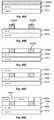
- FIG. 1shows a cross-sectional view of a portion of an exemplary n-type trench power MOSFET
- FIG. 2Ashows an exemplary embodiment of a dual trench power MOSFET
- FIG. 2Bshows an exemplary embodiment for a planar gate MOSFET with source shield trench structure
- FIG. 3Ashows part of an exemplary embodiment of a shielded gate trench power MOSFET
- FIG. 3Billustrates an alternative embodiment for a shielded gate trench power MOSFET that combines the dual trench structure of FIG. 2A with the shielded gate structure of FIG. 3A ;
- FIG. 4Ais a simplified partial diagram of an exemplary embodiment of a dual gate trench power MOSFET
- FIG. 4Bshows an exemplary power MOSFET that combines a planar dual gate structure with trenched electrodes for vertical charge control
- FIG. 4Cshows an exemplary implementation of a power MOSFET that combines the dual gate and shielded gate techniques inside the same trench;
- FIGS. 4D and 4Eare cross-sectional diagrams of alternative embodiments for a power MOSFET with deep body structure
- FIGS. 4F and 4Gillustrate the impact of trenched deep body structures on the distribution of potential lines inside the power MOSFET near the gate electrode
- FIGS. 5A , 5 B and 5 Care cross-sectional diagrams showing portions of exemplary power MOSFETs with various vertical charge balancing structures
- FIG. 6shows a simplified cross-sectional view of a power MOSFET that combines an exemplary vertical charge control structure with a shielded gate structure
- FIG. 7shows a simplified cross-sectional view of another power MOSFET that combines an exemplary vertical charge control structure with a dual gate structure
- FIG. 8shows one example of a shielded gate power MOSFET with vertical charge control structure and integrated Schottky diode
- FIGS. 9A , 9 B and 9 Cdepict various exemplary embodiments for power MOSFETs with integrated Schottky diode
- FIGS. 9D , 9 E and 9 Fillustrate exemplary layout variations for interspersing Schottky diode cells within the active cell array of a power MOSFET
- FIG. 10provides a simplified cross-sectional view of an exemplary trench power MOSFET with buried diode charge balancing structure
- FIGS. 11 and 12show exemplary embodiments for power MOSFETs that combine shielded gate and dual gate techniques with buried diode charge balancing, respectively;
- FIG. 13is a simplified cross-sectional view of an exemplary planar power MOSFET that combines the buried diode charge balancing technique with integrated Schottky diode;
- FIG. 14shows a simplified embodiment of an exemplary accumulation-mode power transistor with alternate conductivity regions arranged in parallel to the current flow
- FIG. 15is a simplified diagram of another accumulation-mode device with trenched electrodes for charge spreading purposes
- FIG. 16is a simplified diagram of an exemplary dual trench accumulation-mode device
- FIGS. 17 and 18show other simplified embodiments for exemplary accumulation-mode devices with dielectric-filled trenches having opposite-polarity exterior liner;
- FIG. 19is another simplified embodiment for an accumulation-mode device that employs one or more buried diodes
- FIG. 20is a simplified isometric view of an exemplary accumulation-mode transistor that includes heavily-doped opposite polarity region along the surface of the silicon;
- FIG. 21shows a simplified example of a super-junction power MOSFET with alternating opposite-polarity regions in the voltage sustaining layer
- FIG. 22shows an exemplary embodiment for a super-junction power MOSFET with opposite-polarity islands non-uniformly spaced in the vertical direction in the voltage sustaining layer;
- FIGS. 23 and 24show exemplary embodiments for super-junction power MOSFETs with dual gate and shielded gate structures, respectively;
- FIG. 25Ashows a top view of active and termination trench layout for a trench transistor
- FIGS. 25B-25Fshow simplified layout views of alternative embodiments for trench termination structures
- FIGS. 26A-26Care cross-sectional views of exemplary trench termination structures
- FIG. 27shows an exemplary device with termination trenches having large radius of curvature
- FIGS. 28A-28Dare cross-sectional views of termination regions with silicon pillar charge balance structures
- FIGS. 29A-29Care cross-sectional views of exemplary embodiments of ultra-high voltage devices employing super-junction techniques
- FIG. 30Ashows an example of edge contacting for a trench device
- FIGS. 30B-30Fshow exemplary process steps in forming the edge contacting structure for a trench device
- FIG. 31Ais an example of an active area contact structure for multiple buried poly layers
- FIGS. 31B-31Mshow an exemplary process flow for forming an active area shield contact structure for a trench
- FIG. 31Nis a cross-sectional view of an alternate embodiment for an active area shield contact structure
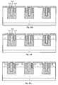
- FIGS. 32A and 32Bare layout views of an exemplary trench device with active area shield contact structure
- FIGS. 32C-32Dare simplified layout diagrams of two embodiments for making contact to the perimeter trench in a trench device with broken trench structure
- FIG. 33Ais an alternate embodiment for contacting trenched shield poly layers in the active area
- FIGS. 33B-33Mshow an example of a process flow for contacting an active area shield structure of the type shown in FIG. 33A ;
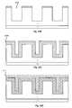
- FIG. 34shows an epi layer having a spacer or buffer (barrier) layer to reduce thickness of epi drift region
- FIG. 35shows an alternative embodiment for a device with a barrier layer
- FIG. 36shows a barrier layer employed at a deep body-epi junction to minimize epi layer thickness
- FIG. 37is a simplified example of the well-drift region junction of a transistor employing a diffusion barrier layer
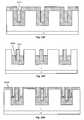
- FIGS. 38A-38Dshow a simplified process flow for an example of a self-aligned epi-well trench device with buried electrode
- FIGS. 39A-39Bshow an exemplary process flow for an angled well implant
- FIGS. 40A-40Eshow an example of a self-aligned epi well process
- FIGS. 40R-40Ushow a method for reducing substrate thickness
- FIG. 41shows an example of a process flow using a chemical process as the final thinning step
- FIGS. 42A-42Fshow examples of improved etch processes
- FIGS. 43A and 43Bshow embodiments of a trench etch process that eliminates the bird's beak problem
- FIGS. 44A and 44Bshow alternative etch processes
- FIG. 45A-45Cshow a process of forming an improved inter-poly dielectric layer
- FIGS. 46A , 46 B and 46 Cillustrate an alternate method of forming an IPD layer
- FIGS. 47A and 47Bare cross-sectional views of yet another method of forming a high quality inter-poly dielectric layer
- FIGS. 48 and 49 A- 49 Dshow other embodiments for formation of an improved IPD layer
- FIG. 50Ashows an anisoptric plasma etch process for IPD planarization
- FIG. 50Bshows an alternate IPD planarization method using a chemical mechanical process
- FIG. 51is a flow diagram for an examplary method for controlling oxidation rate
- FIG. 52shows an improved method for forming thick oxide at the bottom of a trench using a sub-atmospheric chemical vapor deposition process
- FIG. 53is an exemplary flow diagram of a method for forming thick oxide at the bottom of a trench using a directional Tetraethoxyorthsilicate process
- FIGS. 54 and 55show another embodiment for forming thick bottom oxide
- FIGS. 56-59show another process for forming a thick dielectric layer at the bottom of a trench
- FIG. 60is a simplified diagram of a MOSFET with a current sense device
- FIG. 61Ais an example of a charge balance MOSFET with a planar gate structure and isolated current sense structure
- FIG. 61Bshows an example of integrating a current sense device with a trench MOSFET
- FIGS. 62A-62Cshow alternative embodiments for a MOSFET with series temperature sensing diodes
- FIGS. 63A and 63Bshow alternative embodiments for a MOSFET with ESD protection
- FIGS. 64A-64Dshow examples of ESD protection circuits
- FIG. 65shows an exemplary process for forming charge balanced power devices with lower ESR
- FIGS. 66A and 66Bshow a layout technique to reduce ESR
- FIG. 67shows a DC-DC converter circuit using power switching
- FIG. 68shows another DC-DC converter circuit using power switching
- FIG. 69shows an exemplary driver circuit for a dual gate MOSFET
- FIG. 70Ashows an alternate embodiment with separately driven gate electrodes
- FIG. 70Bshows a timing diagram illustrating the operation of the circuit of FIG. 70A ;
- FIG. 71is a simplified cross-sectional view of a molded package.
- FIG. 72is a simplified cross-sectional view of an unmolded package.
- the power switchcan be implemented by any one of power MOSFET, IGBT, various types of thyristors and the like. Many of the novel techniques presented herein are described in the context of the power MOSFET for illustrative purposes. It is to be understood however that the various embodiments of the invention described herein are not limited to the power MOSFET and can apply to many of the other types of power switch technologies, including, for example, IGBTs and other types of bipolar switches and various types of thyristors, as well as diodes. Further, for the purposes of illustration, the various embodiments of the invention are shown to include specific p and n type regions. It is understood by those skilled in the art that the teachings herein are equally applicable to devices in which the conductivities of the various regions are reversed.
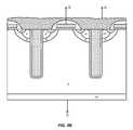
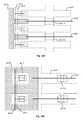
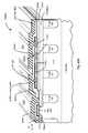
- Trench MOSFET 100includes a gate electrode that is formed inside trenches 102 that extend from the top surface of the substrate through a p-type well or body region 104 , terminating in an n-type drift or epitaxial region 106 .
- Trenches 102are lined with thin dielectric layers 108 and are substantially filled with conductive material 110 such as doped polysilicon.
- N-type source regions 112are formed inside body region 104 adjacent to trenches 102 .
- a drain terminal for MOSFET 100is formed at the backside of the substrate connecting to a heavily-doped n+ substrate region 114 .
- the structure shown in FIG. 1is repeated many times on a common substrate made of, for example, silicon, to form an array of transistors.
- the arraymay be configured in various cellular or striped architectures known in this art.
- a conducting channelis formed vertically between source regions 112 and drift region 106 along the walls of gate trenches 102 .
- MOSFET 100Because of its vertical gate structure, MOSFET 100 enables a higher packing density when compared with a planar gate device, and the higher packing density translates to relatively lower on-resistance.
- p+ heavy body region 118is formed inside p ⁇ well 104 such that at the interface between p+ heavy body 118 and p ⁇ well 104 an abrupt junction is formed.
- electric fields that are generated when voltage is applied to the transistorare moved away from the trenches. This increases avalanche current handling capability of the transistor. Variations on this improved structure and processes for forming the transistor, and in particular the abrupt junction, are described in greater detail in commonly owned U.S. Pat. No. 6,429,481, to Mo et al., which is hereby incorporated by reference in its entirety.
- the input capacitance for trench MOSFET 100has two components: gate-to-source capacitance Cgs and gate-to-drain capacitance Cgd.
- the gate-to-source capacitance Cgsresults from the overlap between gate conductive material 110 and source regions 112 near the top of the trench.
- the capacitance formed between the gate and the inverted channel in the bodyalso contributes to Cgs since in typical power switching applications the body and source electrodes of the transistor are shorted together.
- the gate-to-drain capacitance Cgdresults from the overlap between gate conductive material 110 at the bottom of each trench and drift region 106 which connects to the drain.
- the gate-to-drain capacitance Cgdlimits the transistor V DS transition time. Therefore, higher Cgs and Cgd results in appreciable switching losses. These switching losses are becoming increasingly important as power management applications move toward higher switching frequencies.
- One way to reduce the gate-to-source capacitance Cgsis to reduce the channel length of the transistor.
- a shorter channel lengthdirectly reduces the gate-to-channel component of Cgs.
- a shorter channel lengthis also directly proportional to R DSon and enables obtaining the same device current capacity with fewer gate trenches. This reduces both Cgs and Cgd by reducing the amount of gate-to-source and gate-to-drain overlap.
- a shorter channel lengthrenders the device vulnerable to punch through when the depletion layer formed as a result of the reverse-biased body-drain junction pushes deep into the body region and approaches the source regions. Decreasing the doping concentration of the drift region so that it sustains more of the depletion layer has the undesirable effect of increasing the on-resistance R DSon of the transistor.
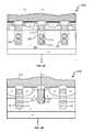
- dual trench MOSFET 200there is shown an exemplary embodiment of a dual trench MOSFET 200 .
- the terminology “dual trench”refers to the transistor having two different types of trenches as opposed to the total number of similar trenches.
- dual trench MOSFET 200includes shield trenches 220 that are interposed between adjacent gate trenches 202 .
- FIG. 1In the exemplary embodiment shown in FIG.
- shield trenches 220extend from the surface through p+ region 218 , body region 204 and into drift region 206 well below the depth of gate trenches 202 .
- Trenches 220are lined with a dielectric material 222 and are substantially filled with conductive material 224 such as doped polysilicon.
- a metal layer 216electrically connects conductive material 224 inside trenches 220 with the n+ source regions 212 and p+ heavy body regions 218 .
- trenches 220can therefore be referred to as source shield trenches.
- An example of this type of dual trench MOSFET, and process of manufacture and circuit applications for the sameare described in greater detail in commonly-assigned, U.S. patent application Ser. No. 10/209,110, entitled “Dual Trench Power MOSFET,” by Steven Sapp, which is hereby incorporated by reference in its entirety.
- the impact of deeper source shield trenches 220is to push the depletion layer formed as a result of the reverse-biased body-drain junction deeper into drift region 206 .
- a wider depletion regioncan result without increasing the electric field.
- Thisallows the drift region to be more highly doped without lowering the breakdown voltage.
- a more highly doped drift regionreduces the transistor on-resistance.
- the reduced electric field near the body-drain junctionallows the channel length to be substantially reduced which further reduces the on-resistance of the transistor and substantially reduces the gate-to-source capacitance Cgs.
- the dual trench MOSFETenables obtaining the same transistor current capacity with far fewer gate trenches.
- gate trench conductive layer 210is buried inside the trench eliminating the need for the interlayer dielectric dome that is present above trenches 102 in MOSFET 100 shown in FIG. 1 .
- the use of source shield trenches as taught hereinis not limited to trench gated MOSFETs and similar advantages are obtained when source shield trenches are employed in planar MOSFETs where the gate is formed horizontally on the top surface of the substrate.
- An exemplary embodiment for a planar gate MOSFET with source shield trench structureis shown in FIG. 2B .
- gate-to-drain capacitance Cgdis caused by the overlap between the gate and the drift region at the bottom of the trench.
- One method of reducing this capacitanceincreases the thickness of the gate dielectric layer at the bottom of the trench.
- gate trenches 202are depicted as having a thicker dielectric layer 226 at the bottom of the trench where there is overlap with drift region 206 (the transistor drain terminal) as compared to dielectric layer along the sidewalls of the gate trench. This reduces the gate-to-drain capacitance Cgd without degrading the forward conduction of the transistor.
- Creating a thicker dielectric layer at the bottom of the gate trenchcan be accomplished in a number of different ways.
- One exemplary process for creating the thicker dielectric layeris described in commonly-owned U.S. Pat. No. 6,437,386 to Hurst et al. which is hereby incorporated by reference in its entirety.
- Other processes for forming a thick dielectric layer at the bottom of a trenchare described further below in connection with FIGS. 56 to 59 .
- Another way to minimize the gate-to-drain capacitanceis to include a centrally disposed second dielectric core inside the trench that extends upwardly from the dielectric liner on the trench floor.
- the second dielectric coremay extend all the way up to contact the dielectric layer above the trench conductive material 210 .
- An example of this embodiment, and variations thereof,are described in greater detail in commonly-owned U.S. Pat. No. 6,573,560 to Shenoy.
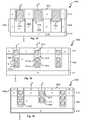
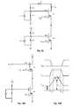
- FIG. 3Athere is shown part of an exemplary embodiment of a shielded gate trench MOSFET 300 A.
- Trenches 302 in MOSFET 300 Ainclude a gate electrode 310 and, in this example, two additional electrodes 311 a and 311 b under gate electrode 310 .
- Electrodes 311 a and 311 bshield gate electrode 310 from having any substantial overlap with drift region 306 almost eliminating the gate-to-drain overlap capacitance.
- Shield electrodes 311 a and 311 bcan be independently biased at optimal potential.
- one of shield electrodes 311 a or 311 bmay be biased at the same potential as the source terminal. Similar to the dual trench structure, the biasing of the shield electrodes can also help in widening of the depletion region formed at the body-drain junction which further reduces Cgd. It is to be understood that the number of shield electrodes 311 can vary depending on the switching application and in particular the voltage requirements of the application. Similarly, the size of the shield electrodes in a given trench can vary.
- shield electrode 311 acan be larger than shield electrode 311 b .
- the smallest shield electrodeis the closest to the bottom of the trench and the remaining shield electrodes gradually increase in size as they near the gate electrode.
- Independently biased electrodes inside trenchescan also be used for vertical charge control purposes to improve smaller forward voltage loss and higher blocking capability.
- This aspect of the transistor structurewhich will be described further below in connection with higher voltage devices, is also described in greater detail in commonly-assigned U.S. patent application Ser. No. 09/981,583, entitled “Semiconductor Structure with Improved Smaller Forward Voltage Loss and Higher Blocking Capability,” by Kocon, which is hereby incorporated by reference in its entirety.
- FIG. 3Billustrates an alternative embodiment for a shielded gate trench MOSFET 300 B that combines the dual trench structure of FIG. 2A with the shielded gate structure of FIG. 3A .
- gate trench 301includes gate poly 310 above shield poly 311 similar to trench 302 of MOSFET 300 A.
- MOSFET 300 Bincludes non-gate trenches 301 that may be deeper than gate trenches 302 for vertical charge control purposes. While the charge control trenches 301 may have a single layer of conductive material (e.g., polysilicon) connecting to the source metal at the top of the trench, as in FIG. 2A , the embodiment shown in FIG.
- conductive materiale.g., polysilicon
- Electrode 3Buses multiple stacked poly electrodes 313 that can be independently biased.
- the number of electrodes 313 stacked in a trenchcan vary depending on the application requirements, as can the sizes of electrodes 313 as shown in FIG. 3B .
- the electrodescan be independently biased or tied together electrically. Also the number of charge control trenches inside a device will depend on the application.
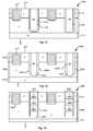
- FIG. 4Ais a simplified partial diagram of an exemplary embodiment of a dual gate trench MOSFET 400 A. As depicted in FIG. 4A , the gate of MOSFET 400 A has two segments G 1 and G 2 .
- the conductive material that forms G 2 in MOSFET 400 Ahas an overlap region 401 with the channel and therefore acts as a gate terminal.
- This secondary gate terminal G 2is biased independently of the primary gate terminal G 1 and does not receive the same signal that drives the switching transistor. Instead, in one embodiment, G 2 is biased at a constant potential just above the threshold voltage of the MOSFET to invert the channel in overlap region 401 . This will ensure that a continuous channel is formed when transitioning from secondary gate G 2 to primary gate G 1 .
- Cgdis reduced because the potential at G 2 is higher than the source potential, and the charge transfer away from the drift region and into the secondary gate G 2 further contributes to the reduction in Cgd.
- secondary gate G 2instead of a constant potential, can be biased to a potential above the threshold voltage just prior to a switching event.
- the potential at G 2can be made variable and optimally adjusted to minimize any fringing portion of the gate-to-drain capacitance Cgd.
- the dual gate structurecan be employed in MOSFETs with planar gate structure as well as other types of trench gate power devices including IGBTs and the like. Variations on the dual gate trench MOS gated devices and processes for manufacturing such devices are described in greater detail in commonly-assigned U.S.
- FIG. 4BAnother embodiment for an improved power MOSFET is shown in FIG. 4B , wherein an exemplary MOSFET 400 B combines a planar dual gate structure with trenched electrodes for vertical charge control.
- Primary and secondary gate terminals G 1 and G 2function in a similar fashion as the trenched dual gate structure of FIG. 4A , while deep trenches 420 provide an electrode in the drift region to spread charge and increase breakdown voltage of the device.
- shield or secondary gate G 2overlaps the upper portion of primary gate G 1 and extends over p well 404 and drift region 406 .
- primary gate G 1extends over shield/secondary gate G 2 .
- the various techniques described thus farsuch as gate shielding and trenched electrodes for vertical charge control can be combined to obtain power devices, including lateral and vertical MOSFETs, IGBTs, diodes and the like, whose performance characteristics are optimized for a given application.
- the trenched dual gate structure shown in FIG. 4Acan be advantageously combined with vertical charge control trench structures of the types shown in FIG. 3B or 4 B.
- Such a devicewould include an active trench with dual gate structure as shown in FIG. 4A as well as deeper charge control trenches that are either substantially filled by a single layer of conductive material (as in trenches 420 in FIG. 4B ) or by multiple stacked conductive electrodes (as in trenches 301 in FIG. 3B ).
- the charge control electrodeswould be laterally disposed forming field plates, instead of being stacked in vertical trenches.
- the orientation of the charge control electrodesis generally parallel to the direction of current flow in the drift region.
- FIG. 4Cshows a MOSFET 400 C wherein trench 402 C includes a primary gate G 1 , a secondary gate G 2 and a shield layer 411 stacked in a single trench as shown.
- Trench 402 Ccan be made as deep and may include as many shield layers 411 as the application demands.
- Using the same trench for both charge balance and shielding electrodesenables higher density, since it eliminates the need for two trenches and combines it into one. It also enables more current spreading and improves device on-resistance. It is to be understood, however, that embodiments combining active trenches having the shielded dual gate structure of the type shown in FIG. 4C with separate charge balancing trenches of the various types described herein are also possible.
- FIG. 4Dthere is shown a partial cross-sectional view of an exemplary embodiment of MOSFET 400 D with deep body design.
- the body structureis formed by a trench 418 that is etched through the center of the mesa formed between gate trenches 402 , and extends as deep or deeper than gate trench 402 .
- Body trench 418is filled with source metal as shown.
- the source metal layermay include a thin refractory metal at the metal-diffusion boundary (not shown).
- the body structurefurther includes a p+ body implant 419 that substantially surrounds body trench 418 .
- P+ implant layer 419enables additional shielding to alter the potential distribution inside the device especially close to the gate electrode.
- body trench 418is substantially filled with epitaxial material using, for example, selective epitaxial growth (SEG) deposition.
- body trench 418 Eis substantially filled with doped polysilicon.
- subsequent temperature treatmentinstead of implanting p+ shield junction 419 , subsequent temperature treatment will diffuse dopants from the filled body into the silicon to form p+ shield junction 419 .
- a number of variations for trenched body structure and formationare described in greater detail in commonly-assigned U.S. Pat. Nos. 6,437,399 and 6,110,799, both to Huang, which are hereby incorporated by reference in their entirety.
- FIGS. 4D and 4Ethe distance L between gate trench 402 and body trench 418 , as well as the relative depths of the two trenches are controlled to minimize fringing gate-to-drain capacitance.
- the spacing between the outer edges of the layer 419 and the wall of the gate trenchcan be adjusted by varying the doping concentration of the SEG or poly inside body trench 418 .
- FIGS. 4F and 4Gillustrate the impact of the trenched deep body on the distribution of the potential lines inside the device near the gate electrode.
- FIGS. 4F and 4Guse MOSFETs with shielded gate structures.
- FIG. 4Fshows the potential lines for a reverse biased shielded gate MOSFET 400 F with trenched deep body 418
- FIG. 4Gshows the potential lines for a reverse biased shielded gate MOSFET 400 G with a shallow body structure.
- the contour lines in each deviceshow potential distribution inside the device when reverse biased (i.e., blocking off-state).
- the white lineshows the well junction and also defines the bottom of the channel located next to the gate electrode.
- the depth of gate trench 402can be reduced to below, e.g., 0.5 um, and can be made shallower than body trench 418 with the spacing L being about 0.5 um or smaller. In one exemplary embodiment, the spacing L is less than 0.3 um.
- Another advantage of this embodimentis the reduction in the gate-drain charge Qgd and Miller capacitance Cgd. The lower the value of these parameters, the faster the device is able to switch. This improvement is realized through the reduction of potential that is present next to the gate electrode. The improved structure has much lower potential that will be switched and the induced capacitive current in the gate is much lower. This in turn enables the gate to switch faster.
- the trenched deep body structure as described in connection with FIGS. 4D and 4Ecan be combined with other charge balancing techniques such as shielded gate or dual gate structures, to further improve the switching speed, on-resistance, and blocking capability of the device.
- Low voltagerefers to a voltage range from, for example, about 30V-40V and below, though this range may vary depending on the particular application. Applications requiring blocking voltages substantially above this range necessitate some type of structural modification to the power transistor.
- the doping concentration in the drift region of the power transistoris reduced in order for the device to sustain higher voltages during the blocking state.
- a more lightly doped drift regionresults in an increase in the transistor on-resistance R DSon .
- the higher resistivitydirectly increases the power loss of the switch. The power loss has become more significant as recent advances in semiconductor manufacturing have further increased the packing density of power devices.
- FIG. 5Ashows a cross-sectional view of a portion of an exemplary power MOSFET 500 A with a planar gate structure.
- MOSFET 500 Aappears to have similar structure to that of planar MOSFET 200 B of FIG. 2B , but it differs from that device in two significant respects.
- these trenchesare filled with dielectric material such as silicon dioxide, and the device further includes discontinuous floating p-type regions 524 spaced adjacent the outer sidewalls of trenches 520 .
- the conductive materiale.g., polysilicon
- the conductive materialin source trenches 202 help improve the cell breakdown voltage by pushing the depletion region deeper into the drift region. Eliminating the conductive material from these trenches would thus result in lowering the breakdown voltage unless other means of reducing the electric field are employed.
- Floating p regions 524serve to reduce the electric field.
- floating p regions 524acquire a corresponding potential determined by their position in the space charge region.
- the floating potential of these p regions 524causes the electric field to spread deeper into the drift region resulting in a more uniform field throughout the depth of the mesa region in between trenches 520 .
- the breakdown voltage of the transistoris increased.
- the advantage of replacing the conductive material in the trenches with insulating materialis that a greater portion of the space charge region appears across an insulator rather than the drift region which could be silicon. Because the permittivity of an insulator is lower than that of, e.g.
- dielectric-filled trenches 520depends on the voltage requirements; the deeper the trenches the higher the blocking voltage.
- An added advantage of the vertical charge control techniqueis that it allows the transistor cells to be laterally displaced for thermal isolation without appreciable added capacitance.
- p-type layersinstead of the floating p regions, line the exterior sidewalls of the dielectrically-filled trenches to achieve similar vertical charge balancing. A simplified and partial cross-sectional view of this embodiment is shown in FIG.
- trench MOSFET 500 B of FIG. 5Bexhibits reduced output capacitance and improved breakdown voltage.
- the active trenchgate trench 502
- the channel width of MOSFET 500 Bis not as large as conventional trench MOSFET structures. This may result in a higher on-resistance R DSon .
- FIG. 5Cthere is shown an alternative embodiment for a trench MOSFET 500 C with vertical charge control that eliminates the secondary charge control trenches.
- Trenches 502 C in MOSFET 500 Cinclude gate poly 510 and a dielectric-filled lower portion that extends deep into drift region 506 .
- trenches 502 Cextend to a depth below about half the depth of drift region 506 .
- a p-type liner 526 Csurrounds the exterior walls along the lower portion of each trench as shown. This single-trench structure eliminates the secondary charge control trench, allowing for increased channel width and lower R DSon .
- the lower portion of deeper trench 502 C that is surrounded by a p-type liner 526 C on its exterior wallssupports a major portion of the electric field in order to reduce output capacitance and gate-to-drain capacitance.
- p-type liner 526 Cis made into a plurality of discontinuous regions along the sides and the bottom of trench 502 C.
- Other embodimentsare possible by combining the single trench charge control structure with shielded gate or dual gate techniques described above, to further reduce device parasitic capacitance.
- MOSFET 600combines vertical charge control to improve breakdown voltage, with shielded gate structure that improves switching speed.
- a shield electrode 611is positioned inside gate trench 602 between gate conductive material 610 and the bottom of the trench. Electrode 611 shields the gate of the transistor from underlying drain region (drift region 606 ) which significantly reduces the gate-to-drain capacitance of the transistor and thus increases its maximum switching frequency.
- Dielectric-filled trenches 620 with p doped liners 626help create a largely flat electric field vertically to improve the breakdown voltage of the device.
- the combination of dielectric-filled trenches 620 with p-type liner 626 , and the shielded gate structurereduces the parasitic capacitance and helps deplete the n drift region which disperses the electric field concentrating on the edge portion of the gate electrode.
- Devices of this typecan be used in RF amplifier or in high frequency switching applications.
- FIG. 7depicts an alternative embodiment for another power MOSFET suitable for higher voltage, higher frequency applications.
- MOSFET 700combines vertical charge control to improve breakdown voltage with dual gate structure that improves switching speed. Similar to the device shown in FIG. 6 , vertical charge control is implemented by the use of dielectric-filled trenches 720 with p-doped liners 726 . Reduction in parasitic capacitance is achieved by the use of a dual gate structure whereby a primary gate electrode G 1 is shielded from the drain (n ⁇ drift region 706 ) by a secondary gate electrode G 2 . Secondary gate electrode G 2 can be either continuously biased or only biased prior to a switching event in order invert the channel in region 701 to ensure an uninterrupted flow of current through a continuous channel when the device is turned on.
- the shielded vertical charge control MOSFETalso employs the doped sidewall dielectric-filed trenches to implement an integrated Schottky diode.
- FIG. 8shows one example of a shielded gate MOSFET 800 according to this embodiment.
- electrode 811 in the lower part of trench 802shields gate electrode 810 from drift region 806 to reduce parasitic gate-to-drain capacitance.
- Dielectric-filled trenches 820 with p doped liners on their exterior sidewallsprovide for vertical charge control.
- a Schottky diode 828is formed between two trenches 820 A and 820 B that form a mesa of width W.
- This Schottky diode structureis interspersed throughout the trench MOSFET cell array to enhance the performance characteristics of the MOSFET switch.
- the forward voltage dropis reduced by taking advantage of the low barrier height of Schottky structure 828 .
- this diodewill have an inherent reverse recovery speed advantage compared to the normal PN junction of the vertical power MOSFET.
- doping of the sidewalls of dielectric-filled trenches 820 with, e.g., Boronsidewall leakage path due to phosphorus segregation is eliminated.
- features of the trench processcan be used to optimize the performance of Schottky diode 828 .
- the width Wis adjusted such that depletion in the drift region of Schottky structure 828 is influenced and controlled by the adjacent PN junction to increase the reverse voltage capability of Schottky diode 828 .
- An example of a monolithically integrated trench MOSFET and Schottky diodecan be found in commonly-assigned U.S. Pat. No. 6,351,018 to Sapp, which is hereby incorporated by reference in its entirety.
- a Schottky diode formed between dielectric-filled trenches of the type depicted in FIG. 8can be integrated with a variety of different types of MOSFETs, including MOSFETs with a planar gate structure, trench gate MOSFETs without any shielding electrode with or without thick dielectric at the bottom of the trench, etc.
- An exemplary embodiment for a dual gate trench MOSFET with integrated Schottky diodeis shown in FIG. 9A .
- MOSFET 900 Aincludes gate trench 902 wherein a primary gate G 1 is formed above a secondary gate G 2 to reduce parasitic capacitance and increase switching frequency.
- MOSFET 900 Aalso includes dielectric-filled trenches 920 with p doped liners 926 formed along their exterior sidewalls for vertical charge control to enhance the device blocking voltage.
- One method of forming the liners for many of the embodiments described aboveuses a plasma doping process.
- Schottky diode 928 Ais formed between two adjacent dielectric-filled trenches 920 A and 920 B as shown.
- a monolithically integrated Schottky diode and trench MOSFETis formed without the dielectric-filled trenches.
- FIG. 9Bis a cross-sectional view of an exemplary device 900 B according to this embodiment.
- MOSFET 900 Bincludes active trenches 902 B each having electrodes 911 buried under a gate electrode 910 .
- a Schottky diode 928 Bis formed between two trenches 902 L and 902 R as shown.
- the charge balancing effect of biased electrodes 911allows for increasing the doping concentration of the drift region without compromising the reverse blocking voltage. Higher doping concentration in the drift region in turn reduces the forward voltage drop for this structure.
- the depth of each trench as well as the number of the buried electrodesmay vary.
- trench 902 Chas only one buried electrode 911 and gate electrodes 910 S in Schottky cell 928 C connect to the source electrode as shown.
- FIGS. 9D , 9 E and 9 Fshow exemplary layout variations for Schottky diode interspersed within the active cell array of MOSFET.
- FIGS. 9D and 9Eshow single mesa Schottky and double mesa Schottky layouts, respectively, while FIG. 9F shows a layout wherein Schottky regions are perpendicular to MOSFET trenches.
- FIG. 10provides a simplified cross-sectional view of an exemplary trench MOSFET 1000 according to this embodiment.
- Diode trenches 1020are disposed on either sides of a gate trench 1002 , extending well into drift region 1006 .
- Diode trenches 1020include one or more diode structures made up of opposite conductivity type regions 1023 and 1025 that form one or more PN junctions inside the trench.
- trench 1020includes a single region having a polarity that is opposite that of the drift region such that a single PN junction is formed at the interface with the drift region.
- P-type and n-type doped polysilicon or siliconmay be used to form regions 1023 and 1025 , respectively.
- Other types of materialsuch as silicon carbide, gallium arsenide, silicon germanium, etc. could also be used to form regions 1023 and 1025 .
- a thin dielectric layer 1021 extending along the trench inner sidewallsinsulates the diode in the trench from drift region 1006 . As shown, there is no dielectric layer along the bottom of trenches 1020 , thus allowing the bottom region 1027 to be in electrical contact with the underlying substrate.
- dielectric layer 1021similar considerations to those dictating the design and manufacture of the gate oxide 1008 are applied in designing and forming dielectric layer 1021 .
- the thickness of dielectric layer 1021is determined by such factors as the voltage it is required to sustain and the extend to which the electric field in the diode trench is to be induced in the drift region (i.e., the extent of coupling through the dielectric layer).
- FIG. 11shows one example of a MOSFET 1100 according to one such embodiment.
- MOSFET 1100uses a shield electrode 1111 inside active trench 1102 under gate electrode 1110 , to reduce gate-to-drain capacitance Cgd for the transistor as described above in connection with, for example, MOSFET 300 A in FIG. 3A .
- a different number of PN junctionsare employed in MOSFET 1100 as compared to MOSFET 1000 .
- FIG. 12is a cross-sectional view of a MOSFET 1200 that combines the dual gate technique with the trenched diode structure.
- Active trench 1202 in MOSFET 1200includes a primary gate G 1 and a secondary gate G 2 and operates in the same manner as the active trenches in the dual gate MOSFET described in connection with FIG. 4B .
- Diode trenches 1220provide charge balancing to increase the device blocking voltage while the dual gate active trench structure improves the device switching speed.
- Yet another embodimentcombines the trenched diode charge balancing technique with integrated Schottky diode in a planar gate MOSFET 1300 as shown in FIG. 13 . Similar advantages can be obtained by the integration of Schottky diode 1328 with the MOSFET as described in connection with the embodiments of FIGS. 8 and 9 .
- a planar gate structureis shown for illustrative purposes, and those skilled in the art will appreciate that the combination of an integrated Schottky diode and trenched diode structure can be employed in a MOSFET having any of the other types of gate structures including trench gate, dual gate and shielded gate.
- any one of the resulting embodimentscan also be combined with the trenched body technique to further minimize the fringing parasitic capacitance, as described in connection with MOSFET 400 D or 400 E of FIGS. 4D and 4E .
- the number of regions of opposite conductivity inside the diode trenchesmay vary as can the depth of the diode trenches.
- the polarities of the opposite conductivity regionsmay be reversed as can the polarity of the MOSFET.
- any of the PN regions923 , 925 or 1023 , 1025 , etc.
- multiple diode trenchesmay be used as demanded by the size of the device and the voltage requirements of the application, and the spacing and arrangement of the diode trenches can be implemented in various stripe or cellular designs.
- a class of accumulation-mode transistorsemploys various charge balancing techniques for smaller forward voltage loss and higher blocking capability.
- a typical accumulation-mode transistorthere is no blocking junction and the device is turned off by lightly inverting the channel region next to the gate terminal to pinch off the current flow.
- an accumulation layerrather than an inversion layer is formed in the channel region. Since there is no inversion channel forming, channel resistance is minimized.
- there is no PN body diode in an accumulation-mode transistorwhich minimizes the losses that are otherwise incurred in certain circuit applications such as synchronous rectifiers.
- the drawback of conventional accumulation-mode devicesis that the drift region has to be lightly doped to support a reverse bias voltage when the device is in blocking mode. A more lightly doped drift region translates to higher on-resistance. Embodiments described herein overcome this limitation by employing various charge balancing techniques in an accumulation-mode device.
- transistor 1400is an n-channel transistor with a gate terminal formed inside trenches 1402 , an n-type channel region 1412 that is formed between trenches, a drift region 1406 that includes opposite polarity columnar n-type and p-type sections 1403 and 1405 , and an n-type drain region 1414 .
- accumulation-mode transistor 1400does not include a blocking (p-type in this example) well or body region inside which the channel is formed. Instead, a conducting channel is formed when an accumulation layer is formed in region 1412 .
- Transistor 1400is normally on or off depending on doping concentration of region 1412 and doping type of the gate electrode. It is turned off when n-type region 1412 is entirely depleted and lightly inverted.
- the doping concentrations in opposite polarity regions 1403 and 1405are adjusted to maximize charge spreading, which enables the transistor to support higher voltages.
- the use of columnar opposite polarity regions parallel to current flowflattens the electric field distribution by not allowing it to decrease linearly away from the junction formed between regions 1412 and 1406 .
- the charge spreading effect of this structureallows the use of a more highly doped drift region which reduces transistor on-resistance.
- n-type regions 1412 and 1403may have the same or different doping concentrations.
- p-channel transistorcan be obtained by reversing the polarities of the various regions of the device shown in FIG. 14 .
- Other variations of the columnar opposite polarity regions inside the drift regionare described in greater detail in connection with ultra-high voltage devices described further below.
- FIG. 15is a simplified diagram of another accumulation-mode device 1500 with trenched electrodes for charge spreading purposes. All regions 1512 , 1506 and 1514 are of the same conductivity type, in this example, n-type. For a normally off device, gate polysilicon 1510 is made p-type. The doping concentration of region 1512 is adjusted to form a depleted blocking junction under no bias conditions. Inside each trench 1502 , one or more buried electrodes 1511 are formed under gate electrode 1510 , all surrounded by dielectric material 1508 . As described in connection with enhancement-mode MOSFET 300 A of FIG. 3A , buried electrodes 1511 act as field plates and can be biased, if desired, to a potential that optimizes their charge spreading function.
- charge spreadingcan be controlled by independently biasing buried electrodes 1511 , the maximum electric field can be increased significantly. Similar to the buried electrodes employed in MOSFET 300 A, different variations of the structure are possible. For example, the depth of trench 1502 and the size and number of buried electrodes 1511 can vary depending on the application. Charge spreading electrodes can be buried inside trenches that are separate from active trenches that house the transistor gate electrode, in a similar fashion to that shown for the trench structures of MOSFET 300 B in FIG. 3B . An example of such an embodiment is shown in FIG. 16 . In the example shown in FIG. 16 , n-type region 1612 includes more heavily doped n+ source regions 1603 that can be optionally added.
- Heavily doped source regions 1603can extend along the top edge of n-type region 1612 as shown or can be formed as two regions adjacent trench walls along the top edge of n-type region 1612 (not shown in this Figure). In some embodiments, the inclusion of n+ regions 1603 may necessitate lowering the doping concentration of n-type region 1606 in order to ensure the transistor can properly shut off. This optional heavily doped source region can be used in the same manner in any one of the accumulation transistors described herein.
- FIG. 17is a simplified cross-sectional view of an accumulation transistor 1700 according to this embodiment.
- Dielectric-filled trenches 1720extend downward from the surface of the silicon well into drift region 1706 .
- Trenches 1720are substantially filed with dielectric material such as silicon dioxide.
- transistor 1700is an n-channel transistor with trenched gate structure.
- a p-type region 1726lines the exterior walls of dielectric-filled trenches 1720 as shown. Similar to the enhancement-mode transistors 500 A, 500 B and 500 C described in connection with FIGS.
- trenches 1720reduce the output capacitance of the transistor while p-type liner 1726 provides for charge balancing in the drift region to increase the blocking capability of the transistor.
- oppositely doped liners 1826 N and 1826 Pare formed adjacent the opposite sides of a dielectric-filled trench 1820 . That is, a dielectric-filled trench 1820 has a p-type liner 1826 P extending along the exterior sidewall on one side, and an n-type liner 1826 N extending along the exterior sidewall on the other side of the same trench.
- a dielectric-filled trench 1820has a p-type liner 1826 P extending along the exterior sidewall on one side, and an n-type liner 1826 N extending along the exterior sidewall on the other side of the same trench.
- an accumulation-mode transistoremploys one or more diodes formed in series inside a trench for charge balancing purposes.
- a simplified cross-sectional view of an exemplary accumulation-mode transistor 1900 according to this embodimentis shown in FIG. 19 .
- Diode trenches 1920are disposed on either side of a gate trench 1902 , extending well into drift region 1906 .
- Diode trenches 1920include one or more diode structures made up of opposite conductivity type regions 1923 and 1925 that form one or more PN junctions inside the trench. P-type and n-type doped polysilicon or silicon may be used to form regions 1923 and 1925 .
- a thin dielectric layer 1921 extending along the trench inner sidewallsinsulates the diodes in the trench from drift region 1906 .
- FIG. 20is a simplified three-dimensional view of an exemplary accumulation-mode transistor 2000 that shows this feature in combination with other variations.
- the charge balancing diodes in accumulation-mode transistor 2000are formed inside the same trench as the gate.
- Trench 2002includes gate electrode 2010 below which n-type 2023 and p-type 2025 silicon or polysilicon layers form PN junctions.
- a thin dielectric layer 2008separates the diode structure from gate terminal 2002 as well as drift region 2006 .
- Heavily doped p+ regions 2118are formed at intervals along the length of the mesa formed between trenches in source regions 2012 , as shown.
- Heavily doped p+ regions 2118reduce the area of n ⁇ region 2012 and reduce device leakage. P+ regions 2118 also allow for p+ contact which will improve hole current flow in avalanche and improve device robustness.
- Variations on an exemplary vertical MOS-gated accumulation transistorhave been discussed to illustrate the various features and advantages of this class of device. One of skill in the art appreciates that these can be implemented in other types of devices including lateral MOS-gated transistors, diodes, bipolar transistors and the like.
- Charge spreading electrodescan be formed either inside the same trench as the gate or inside separate trenches.
- the various exemplary accumulation-mode transistors described abovehave the trenches terminating in the drift regions, but they can also terminate in the more heavily doped substrate connecting to the drain.
- the various transistorscan be formed in stripe or cellular architecture including hexagonal or square shaped transistor cells. Other variations and combinations as described with some of the other embodiments are possible, many of which are further described in previously referenced U.S. Patent Application Nos. 60/506,194 and 60/588,845, both of which are incorporated herein by reference in their entirety.
- MOSFET 2100Another class of power switching devices designed for very high voltage applications (e.g., 500V-600V and above), employs alternating vertical sections of p-doped and n-doped silicon in the epitaxial region between the substrate and the well.
- region 2102that is sometimes referred to as the voltage sustaining or the blocking region, comprises the alternating n-type sections 2104 and p-type sections 2106 .
- the effect of this structureis that when voltage is applied to the device, the depletion region spreads horizontally into each side of sections 2104 and 2106 .
- blocking layer 2102The entire vertical thickness of blocking layer 2102 is depleted before the horizontal field is high enough to produce avalanche breakdown because the net quantity of charge in each vertical section 2104 , 2106 is less than that needed to produce the breakdown field. After the region is fully depleted horizontally, the field continues to build vertically until it reaches the avalanche field of approximately 20 to 30 volts per micron. This greatly enhances the voltage blocking capability of the device extending the voltage range of the device to 400 volts and above. Different variations of this type of super-junction device are described in greater detail in commonly-owned U.S. Pat. Nos. 6,081,009 and 6,066,878 both to Nielson, which are hereby incorporated by reference in their entirety.
- FIG. 22is a simplified cross-sectional view of a MOSFET 2200 that shows one example of a device according to this embodiment.
- the deeper floating p regions 2226are spaced farther from the ones above. That is, the distance L 3 is larger than the distance L 2 , and the distance L 2 is larger than the distance L 1 .
- the number of floating regions 2226 in the vertical directionis not limited to four as shown, and the optimum number may vary.
- the doping concentration in each floating region 2226may vary; for example, in one embodiment, the doping concentration in each floating region 2226 decreases gradually as the region gets closer to substrate 2114 .
- FIG. 23is a simplified cross-sectional view of a high voltage MOSFET 2300 that combines a variation of the super-junction architecture with a dual gate structure.
- MOSFET 2300has a planar dual gate structure made up of gate terminals G 1 and G 2 similar to, for example, the dual gate transistor shown in FIG. 4B above.
- Opposite polarity (p-type in this example) regions 2326are vertically disposed in n-type drift region 2306 under p-well 2308 .
- FIG. 24depicts yet another embodiment for a high voltage MOSFET 2400 that combines the super-junction technology with shielded gate structure.
- MOSFET 2400is a trench gate device with a gate electrode 2410 that is shielded from drift region 2406 with a shield electrode 2411 similar to, for example, MOSFET 300 A in FIG. 3A .
- MOSFET 2400also includes opposite polarity floating regions 2426 disposed in drift region 2406 parallel to current flow.
- Discrete devices of the various types described abovehave a breakdown voltage limited by the cylindrical or spherical shape of the depletion region at the edge of the die. Since this cylindrical or spherical breakdown voltage is typically much lower than the parallel plane breakdown voltage BVpp in the active area of the device, the edge of the device needs to be terminated so as to achieve a breakdown voltage for the device that is close to the active area breakdown voltage.
- Different techniqueshave been developed to spread the field and voltage uniformly over the edge termination width to achieve a breakdown voltage that is close to BVpp. These include field plates, field rings, junction termination extension (JTE) and different combinations of these techniques.
- JTEjunction termination extension
- the termination structureincludes a deep junction (deeper than the well) with an overlying field oxide layer, surrounding the active cell array.
- the termination structureincludes a deep p+ region that forms a PN junction with the n-type drift region.
- FIG. 25Ashows a commonly-used trench layout for a trench transistor. Active trenches 2502 are surrounded by a ring-shaped termination trench 2503 . In this structure, regions 2506 shown by the dotted circles at the ends of the mesas deplete faster than other regions causing increased field in this area which reduces the breakdown voltage under reverse bias conditions. This type of layout is therefore limited to lower voltage devices (e.g., ⁇ 30V).
- FIGS. 25B to 25Fshow a number of alternative embodiments for termination structures with different trench layouts to reduce the high electric field regions shown in FIG. 25A .
- some or all active trenchesare disconnected from the termination trench.
- the gap W G between the ends of the active trenches and the termination trenchfunction to reduce the electric field crowding effect observed in the structure shown in FIG. 25A .
- W Gis made approximately half the width of the mesa between trenches.
- multiple termination trenches as shown in FIG. 25Fcan be employed to further increase the breakdown voltage of the device.
- FIGS. 26A through 26Cdepict cross-sectional views of various exemplary trench termination structures for charge balanced trench MOSFETs.
- MOSFET 2600 Auses a shielded gate structure with a shield poly electrode 2611 buried under gate poly 2610 inside active trench 2602 .
- termination trench 2603 Ais lined with a relatively thick layer of dielectric (oxide) 2605 A and filled with conductive material such as poly 2607 A.
- the thickness of oxide layer 2605 A, the depth of termination trench 2603 A and the spacing between the termination trench and the adjacent active trenchare determined by the device reverse blocking voltage.
- FIG. 1the embodiment shown in FIG.
- trenchesare wider at the surface (T-trench structure) and a metal field plate 2609 A is used over the termination region.
- the field platecan be formed from polysilicon by extending poly 2607 A inside termination trench 2603 A above the surface and over the termination region (to the left of the termination trench in FIG. 26A ).
- a p+ region(not shown) under the metal contacts to silicon can be added for better Ohmic contact.
- P ⁇ well region 2604 in the last mesa adjacent termination trench 2603 A and it's respective contactcan be optionally removed.
- floating p-type region(s)can be added to the left of termination trench 2603 A (i.e., outside active area).
- a poly electrodeis buried in the lower portion of the trench inside an oxide-filled trench.
- This embodimentis shown in FIG. 26B , wherein approximately half of termination trench 2603 B is filled with oxide 2605 B with the lower half having a poly electrode 2607 B buried inside the oxide.
- the depth of trench 2603 B and height of buried poly 2607 Bcan be varied based on the device processing.
- a termination trench 2603 Cis substantially filled with dielectric with no conductive material buried therein. For all three embodiments shown in FIGS.
- the width of the last mesa separating the termination trench from the last active trenchmay be different than the width of a typical mesa formed between two active trenches, and can be adjusted to achieve optimal charge balancing in the termination region. All variations described above in connection with the structure shown in FIG. 26A can apply to those shown in FIGS. 26B and 26C . Further, those skilled in the art appreciate that while the termination structures have been described herein for a shielded gate device, similar structures can be implemented as termination regions for all the various trench based devices described above.
- FIG. 27shows an exemplary device with two termination trenches 2703 - 1 and 2703 - 2 having a relatively larger radius of curvature.
- the spacing between the trenchescan also be adjusted based on the device voltage requirements. In this embodiment, the distance S 1 between termination trenches 2703 - 1 and 2703 - 2 is approximately twice the distance between the first termination trench 2703 - 1 and the end of the active trenches.
- FIGS. 28A , 28 B, 28 C, and 28 Dshow exemplary cross-sectional views for various termination regions with silicon pillar charge balance structures.
- field plates 2809 Acontact every ring of p-type pillar 2803 A. This allows wider mesa regions because of lateral depletion due to field plates.
- the breakdown voltagegenerally depends on the field oxide thickness, the number of rings and the depth and spacing of termination pillars 2803 A. Many different variations for this type of termination structure are possible.
- FIG. 28Bshows an alternative embodiment wherein a large field plate 2809 B- 1 covers all the pillars 2803 B except the last pillar, which is connected to another field plate 2809 B- 2 .
- the termination structurehas no field plates on the middle pillars. Because there is no field plate on the middle pillars, they have narrower mesa region to deplete adequately. In one embodiment, a gradually decreasing mesa width towards the outer ring yields optimal performance.
- the embodiment shown in FIG. 28Dfacilitates contact to p-type pillars by providing a wider well region 2808 D and increasing the spacing between the field oxide layers as shown.
- the breakdown voltageis much higher than the conventional BVpp.
- the charge balance or super-junction structurese.g., opposite polarity pillars or floating regions, buried electrodes, etc.
- Standard edge termination structures in combination with charge balance structures, such as field plates on the top surface at the edge of the devicecan also be used.
- standard edge structures on the topcan be eliminated by using a rapidly decreasing charge in the termination junction.
- p-type pillars in the termination regioncan be formed with decreasing charge the farther they get from the active area creating a net n-type balance charge.
- FIG. 29AA highly simplified cross-sectional view of one exemplary embodiment of a device 2900 A according to this embodiment is shown in FIG. 29A .
- opposite conductivity pillars 2926 Amade of, for example, multiple connected p-type spheres are formed under the p-type well 2908 A in n-type drift region 2904 A.
- p-type termination pillars TP 1 , TP 2 , to TPnare formed as shown.
- the center-to-center spacing between termination pillars TP 1 to TPnincreases as the pillars move farther away from the interface with the active region. That is, distance D 1 between TP 2 and TP 3 is smaller than distance D 2 between TP 3 and TP 4 , and distance D 2 is smaller than distance D 3 between TP 4 and TP 5 , and so on.
- FIG. 29Bshows a simplified example of a termination structure according to this embodiment.
- termination pillar TP 1has a width W 1 that is larger than the width W 2 of termination pillar TP 2 , and W 2 in turn is made larger than the width W 3 of termination pillar TP 3 and so on.
- the resulting structure in device 2900 Bis similar to that of device 2900 A, even though in device 2900 B the center-to-center spacing between trench pillars may be the same.
- the width of each opposite polarity pillar 2926 C in the active regionis decreased from the top surface to the substrate, whereas the width for termination pillars TP 1 and TP 2 remains substantially the same. This achieves the desired breakdown voltage while utilizing less area.
- termination structures described abovecan be combined in any desired manner, including for example, the center-to-center spacing and/or the overall width of termination pillars in device 2900 C shown in FIG. 29C can be varied as described in connection with the embodiments shown in FIGS. 29A and 29B .
- FIG. 30Ashows one example of edge contacting for a trench device 3000 with two poly layers 3010 and 3020 .
- FIG. 30Adepicts a cross-sectional view of the device along the longitudinal axis of a trench.
- FIGS. 30B to 30Fillustrate various processing steps involved in forming the edge contact structure of FIG. 30A .
- a dielectric (e.g., silicon dioxide) layer 3001is patterned on top of epitaxial layer 3006 , and the exposed surface of the substrate is etched to form trench 3002 .
- a first oxide layer 3003is then formed across the top surface of the substrate including the trench as shown in FIG. 30C .
- a first layer of conductive material (e.g., polysilicon) 3010is then formed on top of oxide layer 3003 as shown in FIG. 30D .
- poly layer 3010is etched away inside the trench and another oxide layer 3030 is formed over poly 3010 .
- Similar stepsare carried out to form the second oxide-poly-oxide sandwich as shown in FIG. 30F , where the top oxide layer 3040 is shown as being etched to make openings 3012 and 3022 for metal contact layer to poly layers 3010 and 3020 , respectively.
- the last stepscan be repeated for additional poly layers, and poly layers can be tied together by the overlying metal layer if desired.
- FIG. 31Adepicts one example of the active area contact structure for multiple buried poly layers.
- a cross-sectional view along the longitudinal axis of the trenchshows a poly layer 3110 which provides the gate terminal and poly layers 3111 a and 3111 b that provide two shield layers. While three separate metal lines 3112 , 3122 and 3132 are shown as making contact to the shield poly layers, they can be all tied together and connected to the source terminal of the device, or any other contacting combination can be used as required by a particular application.
- An advantage of this structureis the planar nature of the contact as compared to the multi-layer edge contact structure shown in FIG. 30A .
- FIGS. 31B to 31Millustrate one example of a process flow for forming an active area shield contact structure for a trench with two layers of poly. Etching of trenches 3102 in FIG. 31B is followed by shield oxide 3108 formation in FIG. 31C . Shield polysilicon 3111 is then deposited and recessed inside the trenches as shown in FIG. 31D . Shield poly 3111 is additionally recessed in FIG. 31E , except for locations where shield contact at the surface of the substrate is desired. In FIG. 31E , a mask 3109 protects the poly inside the middle trench from further etch. In one embodiment, this mask is applied at different locations along different trenches such that for the middle trench, for example, shield poly is recessed in other portions of the trench in the third dimension (not shown).
- shield poly 3111 inside one or more select trenches in the active areais masked along the entire length of the trench.
- Shield oxide 3108is then etched as shown in FIG. 31F , and a thin layer of gate oxide 3108 a is then formed across the top of the substrate after mask 3109 is removed as shown in FIG. 31G .
- FIGS. 31K , 31 L and 31 Mdepict the steps of BPSG deposition, contact etch and p+ heavy body implant, followed by metallization, respectively.
- FIG. 31Nshows a cross-sectional view of an alternative embodiment for an active area shield contact structure wherein shield poly 3111 forms a relatively wider platform on top of shield oxide. This facilitates contacting the shield poly, but introduces topography that may further complicate the fabrication process.
- FIG. 32AA simplified top-down layout view of an exemplary trench device with an active area shield contact structure is shown in FIG. 32A .
- a mask defining shield poly recessprevents the recessing of the shield poly at location 3211 C in the active region as well as in perimeter shield trench 3213 .
- a modification of this techniqueuses a “dogbone”-like shape for the shield poly recess mask that provides a wider region at the intersection with each trench 3202 for contact to the shield poly. This allows the shield poly in the masked region to also be recessed but to the original surface of the mesa, thus eliminating topography.
- FIG. 32BThe top-down layout view for an alternative embodiment is shown in FIG. 32B , wherein active area trenches are connected to the perimeter trench.
- FIGS. 32C and 32Dare simplified layout diagrams showing two different embodiments for making contact to the perimeter trench in a trench device with broken trench structure.
- active trenches 3202 and perimeter trench 3213are depicted by a single line for illustrative purposes.
- extensions or fingers from perimeter gate poly runner 3210are staggered with respect to perimeter shield poly fingers to space the perimeter contacts away from the perimeter trench.
- Source and shield contact area 3215also makes contact to shield poly in the active region in locations 3211 C as shown. The embodiment shown in FIG.
- 32Deliminates the offset between active and perimeter trenches to avoid possible limitations arising from trench pitch requirements.
- active trenches 3202 and horizontal extensions from perimeter trench 3213are aligned, and windows 3217 in gate poly runner 3210 allow for contacts to be made to shield poly around the perimeter.
- Active area contactsare made in locations 3211 C as in previous embodiments.
- FIG. 33AAn alternative embodiment for contacting trenched shield poly layers in the active area is shown in FIG. 33A .
- shield poly 3311splits gate poly 3310 into two as it extends vertically along the height of trench 3302 .
- the two gate poly segmentsare connected in the third dimension at a suitable location inside the trench or as they exit the trench.
- FIGS. 33B to 33Millustrate one example of a process flow for forming an active area shield contact structure of the type shown in FIG. 33A .
- Etching of trenches 3302 in FIG. 33Bis followed by shield oxide 3308 formation in FIG. 33C .
- Shield polysilicon 3311is then deposited inside the trenches as shown in FIG. 33D .
- Shield poly 3311is etched and recessed inside the trenches as shown in FIG. 33E .
- Shield oxide 3308is then etched as shown in FIG. 33F , leaving an exposed portion of shield polysilicon 3311 that forms two troughs on its sides inside the trench.
- a thin layer of gate oxide 3308 ais then formed across the top of the substrate, sidewalls of the trenches and troughs inside the trenches as shown in FIG. 33G . This is followed by gate poly deposition and recess ( FIG.
- FIGS. 33K , 33 L and 33 Mdepict the steps of BPSG deposition, contact etch and p+ heavy body implant, followed by metallization, respectively. Variations on this process flow are possible. For example, by re-ordering some of the process steps, the process steps forming gate poly 3310 can be conducted prior to the steps forming shield poly 3311 .
- Transistor specific on-resistancecan be significantly reduced if the device is fabricated in a material with critical field higher than that of silicon, provided that reasonable mobility is maintained. While many of the power devices features, including structures and processes, described thus far have been described in the context of a silicon substrate, other embodiments using substrate material other than silicon are possible. According to one embodiment, the power devices described herein are fabricated in a substrate made of wide-bandgap material, including for example, silicon carbide (SiC), gallium nitride (GaN), gallium arsenide (GaAs), indium phosphide (InP), diamond and the like. These wide-bandgap materials exhibit a critical field that is higher than the critical field for silicon and can allow for a significant reduction in transistor on-resistance.
- SiCsilicon carbide
- GaNgallium nitride
- GaAsgallium arsenide
- InPindium phosphide
- the drift regionis typically formed by epitaxially grown silicon. To reduce R DSon , it is desirable to minimize the thickness of this epi drift region.
- the thickness of the epi layeris dictated in part by the type of starting substrate. For example, a red-phosphorus doped substrate is a common type of starting substrate material for discrete semiconductor devices. A property of phosphorus atoms, however, is that they diffuse quickly in silicon. The thickness of the epi region that is formed on top of the substrate is therefore determined to accommodate the up-diffusion of phosphorus atoms from the underlying heavily doped substrate.
- an epi spacer or buffer (or barrier) layer 3415 having dopants with relatively less diffusivity such as Arsenicis formed above a phosphorus substrate 3414 .
- the combined phosphorous-doped substrate and Arsenic-doped buffer layerprovides the foundation for the subsequent formation of epi drift region 3406 .
- the Arsenic dopant concentration in layer 3415is determined by the breakdown voltage requirements of the device, and the thickness of Arsenic epi layer 3415 is determined by specific thermal budget.
- a regular epi layer 3406may then be deposited on top of the Arsenic epi, the thickness of which would be determined by device requirements. The much lower diffusivity of Arsenic allows the overall thickness of the epi drift region be reduced resulting in a reduction in transistor on-resistance.
- a diffusion barrieris employed between the two layers.
- a barrier layer 3515composed of, e.g., silicon carbide Si x C 1-x is deposited epitaxially on either boron or phosphorus substrates 3514 .
- Epi layer 3506is then deposited atop barrier layer 3515 .
- the thickness and carbon compositionmay vary according to the thermal budget of the process technology. Alternately, carbon dopants can be first implanted into substrate 3514 , after which thermal treatment activates the carbon atoms to form a Si x C 1-x compound at the surface of substrate 3514 .
- junction formed between the deep body and epi layerthat is sometimes employed in the active region and sometimes in the termination region.
- the formation of this deep body regioncommonly involves an implant step early in the process. Due to the large subsequent thermal budget required by the formation of field oxide and gate oxide, the junction at the deep body and drift region is graded to a large extent. To avoid early breakdown at the edge of the die, a much thicker drift region is needed which results in higher on-resistance.
- the use of a diffusion barrier layercan also be employed at the deep body-epi junction in order to minimize the required epi thickness. According to an exemplary embodiment shown in FIG.
- FIG. 37A simplified example of an embodiment employing such a barrier layer is shown in FIG. 37 .
- a p-wellis formed between the two steps shown in FIGS. 31H and 31I .
- layer 3715Prior to implanting the well dopants (p-type for this exemplary n-channel embodiment), carbon is implanted first. The subsequent thermal process activates the carbon atoms to form a layer 3715 of Si x C 1-x at the p-well epi junction. Layer 3715 serves as a diffusion barrier to prevent boron diffusion so that the depth of p-well 3704 can be preserved. This helps reduce transistor channel length without increasing the potential for reach-through. Reach-through occurs when the edge of the advancing depletion boundary reaches the source junction as the drain-source voltage increases. By acting as a diffusion barrier, layer 3715 also prevents reach-through.
- transistor channel lengthis minimized by forming the well region using epitaxially grown silicon. That is, instead of the conventional method of forming the well that involves an implant into the drift epi layer followed by a diffusion step, the well region is formed on top of the epi drift layer.
- advantages other than a shorter channel length that can be obtained from an epi-well formationIn shielded gate trench transistors, for example, the distance by which the gate electrode extends below the bottom of the well where it meets the trench (gate to drain overlap) is critical in determining gate charge Qgd. Gate charge Qgd directly impacts the switching speed of the transistor. It is desirable, therefore, to be able to accurately minimize and control this distance. However, in fabrication processes where the well is implanted and diffused into the epi as shown, for example, in FIG. 31I above, this distance is difficult to control.
- a process flow involving deposition of an epi-wellenables the self-alignment of the bottom of the body junction to the bottom of the gate.
- FIGS. 38A-38Dthere is shown a simplified process flow for one example of a self-aligned epi-well trench device with buried electrode (or shielded gate).
- a trench 3802is etched into a first epi layer 3806 that is formed on top of substrate 3814 .
- substrate 3814 and first epi layer 3806are of n-type material.
- FIG. 38Ashows a layer of shield dielectric 3808 S grown on the top surface of epi layer 3806 including inside trench 3802 .
- Conductive material 3811such as polysilicon is then deposited inside trench 3802 and etched back below the epi mesa as shown in FIG. 38B .
- Additional dielectric material 3809 Sis deposited to cover shield poly 3811 .
- a second layer of epi 3804is selectively grown on top of first epi layer 3806 , as shown in FIG. 38C .
- the mesas formed by epi layer 3804create an upper trench portion above original trench 3802 as shown.
- This second epi layer 3804has dopants of opposite polarity (e.g., p-type) to that of the first epi layer 3806 .
- the dopant concentration in second epi layer 3804is set to the desired level for the transistor well region.
- SEGselective epi growth
- a layer of gate dielectric 3808 Gis formed on the top surface and along the trench sidewalls.
- Gate conductive material(poly) is then deposited to fill the remaining portion of trench 3802 , and then planarized as shown in FIG. 38D .
- the processcontinues as in, for example, the process flow shown in FIGS. 31J to 31M to complete the transistor structure.
- this processresults in gate poly 3810 that is self-aligned with well epi 3804 .
- the top surface of inter-poly dielectric layer 3809 S as shown in FIG. 38Ccan be etched slightly to the desired location inside trench 3802 . This process, therefore, provides for accurate control of the distance between the bottom of the gate electrode and the well corner.
- the SEG well formation processis not limited to a shielded gate trench transistor and can be employed in many other trench gate transistor structures several of which have been described herein. Other methods of forming SEG mesa structures are described in commonly-assigned U.S. Pat. Nos. 6,391,699 to Madson et al. and 6,373,098, to Brush et al., which are hereby incorporated by reference in their entirety.
- FIGS. 39A and 39Billustrate an exemplary process flow for this embodiment.
- a first well implant 3905 at a given partial doseis performed after embedding shield poly in dielectric layer 3908 inside trench 3902 and before the remaining portion of the trench is filled.
- a second but angled well implantis then performed through the sidewalls of trench 3902 as shown in FIG. 39B .
- the drive cycleis then completed to obtain the desired contour for the well to drift epi interface at the trench corner.
- the implant dose, energy and the particulars of the drive cycleswill vary depending on the structural requirements of the device. This technique can be employed in a number of different device types.
- the trench pitch and the angle implantare adjusted such that when the angle implant is diffused, it merges with the region from a neighboring cell to form a continuous well, eliminating the need for the first well implant.
- FIGS. 40A to 40EAnother embodiment for a self-aligned epi well process for forming a trench device is described in connection with FIGS. 40A to 40E .
- some trench gate transistorsemploy a gate dielectric layer that is thicker at the bottom of the trench below the gate poly than the dielectric layer along the inner vertical sidewalls.
- a dielectric layer 4008 Bis first formed on top of an epi drift layer 4006 as shown in FIG. 40A .
- Dielectric layer 4208 Bis formed with the desired thickness for the bottom of the trench, and is then etched leaving dielectric columns, as shown in FIG. 40B , that have the same width as the trench that will subsequently be formed.
- Second drift epi layer 4006 - 1is of the same conductivity type and can be of the same material as the first epi drift layer 4006 .
- second drift epi layer 4006 - 1is formed by an SEG step strained with a silicon germanium (Si x Ge 1-x ) alloy.
- the SiGe alloyimproves the carrier mobility at the accumulation region near the bottom of the trench. This improves the switching speed of the transistor and reduces R DSon .
- the use of other compounds such as GaAs or GaNare also possible.
- a blanket epi well layer 4004is then formed on the top surface, and is then etched to form trenches 4002 as shown in FIGS. 40D and 40E , respectively. This is followed by gate oxide formation and gate poly deposition (not shown). The resulting structure is a trench gate with a self-aligned epi well. Conventional processing techniques can be used to complete the remaining process steps. Those skilled in the art appreciate that variations are possible. For example, instead of forming a blanket epi well layer 4004 and then etching trenches 4002 , epi well 4002 can be selectively grown only on top of second drift epi layer 4006 - 1 forming trenches 4002 as it grows.
- the various processing techniques described aboveenhance device performance by focusing on the formation of the well region to reduce channel length and R DSon . Similar enhancements can be achieved by improving other aspects of the process flow. For example, device resistance can be further reduced by reducing the substrate thickness. A wafer thinning process is therefore commonly performed in order to reduce the thickness of the substrate. Wafer thinning is typically performed by mechanical grind and tape processes. The grind and tape processes impose mechanical forces on the wafer that cause damage to the wafer surface resulting in manufacturing problems.
- an improved wafer thinning processsignificantly reduces substrate resistance. Illustrated in FIGS. 40R , 40 S, 40 T and 40 U, is one method for reducing the thickness of the substrate. After finishing the fabrication of the desired circuitry on a wafer, the top of the wafer where the circuitry is fabricated is temporarily bonded to a carrier.
- FIG. 40Rshows a finished wafer 4001 that is bonded to a carrier 4005 by a bonding material 4003 . The backside of the finished wafer is then polished to the desired thickness using a process such as grinding, chemical etching or the like.
- FIG. 40Sshows the same sandwich as FIG. 40R with finished wafer 4001 having been thinned.
- the backside of the waferis bonded to a low resistance (e.g., metal) wafer 4009 as shown in FIG. 40T .
- a low resistance wafer 4009e.g., metal
- Carrier 4005is then removed and the top surface of thinned finished wafer 4001 is cleaned before further processing.
- the highly conductive metal substrate 4009facilitates heat dissipation, reduction in resistance and provides mechanical strength for the thinned wafer.
- FIG. 41sets out an exemplary process flow according to this embodiment. Starting from a silicon substrate, first at step 4110 a dopant such as, e.g., He or H 2 is implanted into the silicon substrate. Next, at 4112 , the silicon substrate is bonded to a glass substrate. Different bonding processes can be used.
- a dopantsuch as, e.g., He or H 2 is implanted into the silicon substrate.
- the silicon substrateis bonded to a glass substrate. Different bonding processes can be used.
- a silicon wafer and a glass waferare sandwiched and heated up to around, e.g., 400 C to bond the two substrates.
- the glasscan be, e.g., silicon dioxide and the like, and may have a thickness of, for example, about 600 um.
- the bonding processcan be repeated to form SOTG layer on the other side of the substrate (step 4116 ).
- An epi layeris next deposited on the silicon surface of the substrate (step 4118 ). This can be performed on the backside in addition to the front side.
- the doping level of the backside epiis preferably similar to that of the backside silicon, while the front-side epi is doped as required by the device.
- the substrateis then subjected to the various steps in the fabrication process for forming the active device on the front-side silicon layers.
- the backside substratecan be patterned to approximate an inverse structure of the front-side die frame.
- the glass substrateis etched into a grid to help the thin substrate sustain the stress in the wafer.
- a conventional grinding processstep 4120
- another grinding step 4122that removes a portion (e.g., half) of the glass.
- the remaining portion of the glassis then removed by a chemical etch process using, e.g., hydrofluoric acid.
- the etching of the backside glasscan be performed without the risk of attacking or causing mechanical damage to active silicon layers.
- this processallows for further minimizing substrate thickness to enhance device performance. It is to be understood that many variations of this improved wafer thinning process are possible. For example, depending on the desired thickness for the final substrate, the thinning step may or may not involve grinding and chemical etch may be sufficient. Also, the improved wafer thinning process is not limited to processing of discrete devices and can be utilized in the processing of other types of devices. Other wafer thinning processes are described in commonly-assigned U.S. Pat. No. 6,500,764, to Pritchett, which is hereby incorporated in its entirety.
- the shape of the trenchis one example.
- the different etch chemistriesoffer trade-offs among several responses, such as: silicon etch rate, selectivity to the mask layer, etch profile (sidewall angle), top corner rounding, sidewall roughness, and rounding of the trench bottom.
- a fluorinated chemistry, for example SF6provides a high silicon etch rate (greater than 1.5 um/min), rounded trench bottoms, and a straight profile.
- the drawbacks of the fluorinated chemistryare rough sidewalls and difficulties with control of the top of the trench (can be re-entrant).
- a chlorinated chemistryfor example Cl 2 , provides smoother sidewalls, and better control of the etch profile and the top of the trench.
- the trade-offs with the chlorinated chemistryare lower silicon etch rate (less than 1.0 um/min), and less rounding of the trench bottom.
- Additional gasescan be added to each chemistry to aid in passivating the sidewall during the etch.
- Sidewall passivationis used to minimize lateral etching, while etching to the desired trench depth.
- Additional processing stepscan be used to smooth the trench sidewalls, and achieve rounding of the top corner and the bottom of the trench.
- the surface quality of trench sidewallsis important because it affects the quality of an oxide layer that can be grown on the trench sidewall.
- a breakthrough stepis typically used before the main etch step. The purpose of the breakthrough step is to remove any native oxide on the surface of the silicon that may mask the etching of the silicon during the main etch step. Typical breakthrough etch chemistries involve CF 4 or Cl 2 .
- One embodiment for an improved etch process shown in FIG. 42Aemploys a chlorine based main silicon trench etch followed by a fluorine based etch step.
- a chlorine based main silicon trench etchfollowed by a fluorine based etch step.
- This processemploys Cl 2 /HBr main etch step followed by an SF 6 etch step.
- the chlorinated stepis used to etch the main trench to a portion of the desired depth. This defines the trench profile with some degree of taper, and with smooth sidewalls.
- the subsequent fluorinated stepis used to etch the remainder of the trench depth, rounding the trench bottom, and providing further smoothing of any dangling silicon bonds on the trench sidewall.
- the fluorinated etch stepis preferably performed at relatively low fluorine flow, low pressure, and low power to control the smoothing and the rounding.
- the times of the two stepscan be balanced to achieve a more reliable and manufacturable process with an acceptable overall etch time, while maintaining the desired trench profile, sidewall roughness, and trench bottom rounding.
- an improved method for silicon etchincludes a fluorine based main etch step followed by a chlorine based second etch step.
- a fluorine based main etch stepuses an SF 6 /O 2 main etch followed by a Cl 2 step.
- the fluorine stepis used to etch the main trench for the majority of the depth. This step produces a trench with a straight sidewall and with a rounded trench bottom.
- oxygencould be added to this step to provide sidewall passivation, and to aid in maintaining a straight sidewall by reducing lateral etching.
- a chlorine follow-up steprounds the top corners of the trench and reduces the roughness of the sidewall.
- the high silicon etch rate of the fluorine stepincreases the manufacturability of the process by increasing the throughput of the etch system.
- an improved silicon etch processis obtained by adding argon to a fluorine based chemistry.
- a fluorine based chemistryused for the main etch step according to this embodiment is SF 6 /O 2 /Ar.
- the addition of argon to the etch stepincreases ion bombardment and therefore makes the etch more physical. This helps with controlling the top of the trench, and eliminates the tendency for the top of the trench to be re-entrant.
- the addition of argonmay also increase the rounding of the trench bottom.
- An additional etch processmay be needed for sidewall smoothing.
- An alternative embodiment for an improved silicon etch processuses a fluorine based chemistry with oxygen removed from the start of the main etch step, as shown in FIG. 42D .
- One example of this processuses an SF 6 step followed by an SF 6 /O 2 step.
- the first phase of the etchthere is a lack of sidewall passivation due to the absence of O 2 .
- the second etch step, SF 6 /O 2continues etching the remainder of the trench depth with a straight profile, and a rounded trench bottom. This results in a trench structure that is wider at the top, sometimes referred to as a T-trench.
- Additional processing methodscould include, for example: (1) a fluorine-based step at the end of the trench etch recipe, or (2) a separate fluorine-based etch on a separate etch system, or (3) a sacrificial oxide, or any other combination.
- a chemical mechanical planarization (CMP) stepcould be used to remove the top re-entrant portion of the trench profile.
- An H 2 annealcan also be used to assist in rounding and making favorable slope trench profile.
- the silicon etch rateis important to produce a manufacturable process.
- the etch chemistry for this applicationis typically a fluorinated chemistry, because a chlorinated etch chemistry is too slow.
- a straight-to-tapered trench profileis desired, with smooth sidewalls. Due to the depth of the trench, the etch process needs to also have excellent selectivity to the mask layer. If the selectivity is poor then a thicker mask layer is required, which increases the overall aspect ratio of the feature.
- Sidewall passivationis also very critical; a fine balance needs to be achieved. Too much sidewall passivation will cause the bottom of the trench to narrow to the point where it closes; too little sidewall passivation will result in the increased lateral etching.
- a deep trench etch processis provided that optimally balances all of these requirements.
- the etch processincludes a fluorine-based chemistry with ramped O 2 , ramped power, and/or ramped pressure.
- One exemplary embodimentuses a SF 6 /O 2 etch step in a manner that maintains etch profile and silicon etch rate throughout the etch. By ramping the O 2 , the amount of sidewall passivation can be controlled throughout the etch to avoid increased lateral etching (in case of too little passivation) or pinching off of the bottom of the trench (in case of too much passivation).
- An exemplary process according to this embodiment for trenches that are deeper than, e.g., 10 ⁇ m,may have an O 2 flow rate of 3 to 5 sccm per minute, at a power level of 10-20 watts per minute and pressure level of 2-3 mT per minute.
- An alternative embodiment of a deep trench etch processuses a more aggressive fluorine based chemistry such as NF 3 . Since NF 3 is more reactive than SF 6 for silicon etching, an increased silicon etch rate could be achieved with an NF3 process. Additional gases may need to be added for sidewall passivation and profile control.
- NF 3fluorine based chemistry
- an NF 3 etch stepis followed by an SF 6 /O 2 process.
- the NF 3 stepis used to etch the majority of the trench depth with a high silicon etch rate.
- the SF 6 /O 2 etch stepis used to passivate the existing trench sidewall, and etch the remaining portion of the trench depth.
- NF 3 and SF 6 /O 2 etch stepsare performed in an alternating fashion. This yields a process with a higher silicon etch rate than a straight SF 6 /O 2 process.
- a trench etch maskis formed on the surface of the silicon and is patterned to expose areas to be trenched.
- the trench etchfirst etches through a layer of nitride 4305 and another thin layer of pad oxide 4303 before it etches the silicon substrate.
- pad oxide 4303can also grow at the edge of the trench lifting the overlying nitride layer. This results in what is commonly referred to as a “bird's beak” structure 4307 as the pad oxide grows locally near the trench edge under nitride layer 4305 .
- a layer of non-oxidizing material such as polysilicon 4309is sandwiched between nitride layer 4305 and pad oxide 4303 .
- Poly layer 4309prevents pad oxide 4303 from further oxidization during subsequent trench oxide formation.
- a thin layer of non-oxidizing material 4405 - 1such as nitride is formed on the surface structure.
- Protective layer 4405 - 1is then removed from the horizontal surfaces leaving spacers along the vertical edges of the nitride-pad oxide structure as shown in FIG. 44B .
- the nitride spacersprotect pad oxide 4403 from further oxidation during subsequent steps reducing the bird's beak effect.
- both embodiments shown in FIGS. 43B and 44Bcan be combined. That is, a layer of polysilicon can be sandwiched between pad oxide and the overlying nitride in addition to the spacers that result from the process described in connection with FIGS. 44A and 44B .
- Other variationsare possible, including, for example, adding another layer (e.g., oxide) on top of the nitride to aid in the nitride selectivity while etching silicon trenches.
- a layer of dielectric materialisolates the shield electrode from the gate electrode.
- This inter-electrode dielectric layerthat is sometimes referred to as the inter-poly dielectric or IPD must be formed in a robust and reliable fashion so that it can withstand the potential difference that may exist between the shield electrode and the gate electrode.
- FIGS. 31E , 31 F and 31 Gthere is shown a simplified flow for the relevant process steps. After the etch back of shield poly 3111 inside the trench ( FIG. 31E ), shield dielectric layer 3108 is etched back to the same level as shield poly 3111 ( FIG. 31F ). Gate dielectric layer 3108 a is then formed on the top surface of the silicon as shown in FIG.
- a polycrystalline silicon (poly) liner 4508 Pis deposited as shown in FIG. 45B using, for example, a low pressure chemical vapor deposition (LPCVD) process.
- poly liner 4508 Pcan be formed only over the shield poly and shield dielectric and leaving trench sidewalls substantially free of poly by using a selective growth process for poly or collimated sputtering of poly.
- Poly liner 4508 Pis subsequently oxidized converting it into silicon dioxide. This can be performed by a conventional thermal oxidation process. In the embodiment where no poly is formed on the trench sidewalls, this oxidation process also forms gate dielectric layer 4508 G.
- gate dielectric 4508 Gis formed and the remaining trench cavity is filled with gate electrode 4510 as shown in FIG. 45C .
- An advantage of this processis that poly deposits in a very conformal fashion. This minimizes voids and other defects and creates a more even surface once poly is deposited on top of the shield dielectric and shield electrode. The result is an improved IPD layer that is more robust and reliable. By lining the trench sidewalls and the adjacent silicon surface areas with polysilicon prior to oxidation, a subsequent oxidation step causes less mesa consumption and minimizes undesirable widening of the trench.
- the cavity inside the trench resulting from the shield poly recess etchis filled with a dielectric fill material 4608 F having similar etch rate as the etch rate of shield dielectric 4608 S.
- This stepmay be carried out using any one of high density plasma (HDP) oxide deposition, chemical vapor deposition (CVD) or spin-on glass (SOG) processes, followed by a planarization step to obtain a planar surface at the top of the trench.
- Dielectric fill material 4608 F and shield dielectric material 4608 Sare then uniformly etched back such that a layer of insulating material having the requisite thickness remains over shield electrode 4611 as shown in FIG. 46B .
- the trench sidewallsare then lined with gate dielectric after which the remaining trench cavity is filled with gate electrode as shown in FIG. 46C .
- the resultis a highly conformal IPD layer that is free of topographical non-uniformities.
- FIGS. 47A and 47BAn exemplary embodiment for another method of forming high quality IPD is shown in the simplified cross-sectional views of FIGS. 47A and 47B .
- a shield poly etch back stepis performed to recess the shield poly inside the trench.
- the shield poly recess etchleaves more poly in the trench such that the top surface of the recessed shield poly is higher than the final target depth.
- the thickness of the extra poly on the top surface of the shield polyis designed to be approximately the same as the target IPD thickness. This upper portion of the shield electrode is then physically or chemically altered to further enhance its oxidation rate.
- a method to chemically or physically alter the electrodecan be performed by ion implanting impurities such as fluorine or argon ions into the polysilicon to enhance the oxidation rate of the shield electrode, respectively.
- the implantis preferably performed at zero degrees, i.e., perpendicular to the shield electrode as shown in FIG. 47A , so as not to physically or chemically alter the trench sidewalls.
- shield dielectric 4708 Sis etched to remove the dielectric from the trench sidewalls. This shield dielectric recess etch causes a slight recess in the remaining shield dielectric adjacent shield electrode 4711 (similar to that shown in FIG. 45A ).
- shield poly 4711oxidizes at a faster rate than the sidewalls of the trench.
- the thicker insulator 4708 T over the shield electrodeforms the IPD.
- the altered polyoxidizes in the lateral direction as well compensating for some of the trough formed in the top surface of the shield dielectric as a result of the shield dielectric recess etch.
- Conventional stepsare then carried out to form the gate electrode in the trench resulting in the structure shown in FIG. 47B .
- the shield electrodeis altered to obtain an IPD-to-gate oxide thickness ratio in the range of 2-to-1 to 5-to-1.
- an IPD-to-gate oxide thickness ratioin the range of 2-to-1 to 5-to-1.
- a 4-to-1 ratiois selected, for about 2000 ⁇ of IPD formed over the shield electrode, about 500 ⁇ of gate oxide is formed along the trench sidewalls.
- the physical or chemical alternation stepis carried out after a shield dielectric recess etch. That is, shield oxide 4708 S is etched to remove the oxide from the trench sidewalls. This exposes the upper portion of the shield electrode and the silicon to a physical or chemical alteration method as described above. With the trench sidewalls exposed, the alteration step is confined to horizontal surfaces, i.e. silicon mesa and shield electrode only.
- the alteration methodsuch as ion implanting of dopants, would be performed at zero degrees (perpendicular to the shield electrode) so as not to physically or chemically alter the trench sidewall. Conventional steps are then carried out to form the gate electrode in the trench thus resulting in a thicker dielectric over the shield electrode.
- FIG. 48Yet another embodiment for forming an improved IPD layer is shown in FIG. 48 .
- a thick insulator layer 4808 Tmade of, e.g., oxide, is formed over the recessed shield oxide 4808 S and shield electrode 4811 .
- Thick insulator 4808 Tis preferentially formed (i.e., “bottom up fill”) using such directional deposition techniques as high density plasma (HDP) deposition or plasma-enhanced chemical vapor deposition (PECVD).
- PECVDplasma-enhanced chemical vapor deposition
- Directional depositionresults in the formation of a substantially thicker insulator along the horizontal surfaces (i.e., over the shield electrode and the shield oxide) than along the vertical surfaces (i.e., along the trench sidewalls) as shown in FIG. 48 .
- An etch stepis then performed to remove the oxide off the sidewalls, while leaving sufficient oxide over the shield polysilicon. Conventional steps are then carried out to form the gate electrode in the trench.
- a thin layer of screen oxide 4908 Pis grown inside the trench.
- a layer of silicon nitride 4903is deposited to cover screen oxide 4908 P as shown in FIG. 49A .
- Silicon nitride layer 4903is then anisotropically etched such that it is removed from the bottom surface of the trench (i.e., above shield poly) but not from the trench sidewalls.
- the resulting structureis shown in FIG. 49B .
- the waferis then exposed to an oxidizing ambient, causing a thick oxide 4908 T to form on the shield polysilicon surface as shown in FIG. 49C .
- Nitride layer 4903is resistant to oxidation, no significant oxide growth occurs along the trench sidewalls. Nitride layer 4903 is then removed by wet etching, using for example hot phosphoric acid. Conventional process steps follow to form the gate oxide and gate dielectric, as shown in FIG. 49D .
- the formation of the IPD layerinvolves an etch process.
- a film layer much thicker than the desired final IPD thicknessmay be deposited first. This is done to get a planar film layer to minimize the dishing of the starting layer into the trenches.
- the thicker film, which may completely fill the trench and extend over the silicon surface,is then etched to reduce its thickness to the target IPD layer thickness.
- this IPD etch processis performed in at least two etch steps. The first step is intended to planarize the film back to the silicon surface. In this step the uniformity of the etch is important.
- the second stepis intended to recess the IPD layer to the desired depth (and thickness) within the trench.
- the etch selectivity of the IPD film to siliconis important.
- the silicon mesais exposed, as well as the silicon trench sidewall as the IPD layer is recessed into the trench. Any loss of silicon on the mesa affects the actual trench depth and, if a T-trench is involved, the depth of the T is also affected.
- an anisotropic plasma etch step 5002is used to planarize the IPD film down to the surface of the silicon.
- An exemplary etch rate for the plasma etchmay be 5000 A/min.
- the wet etchis preferably performed using a controlled solution selective to silicon so as not to attack the silicon sidewall when exposed and to provide a repeatable etch to obtain a specific recess depth.
- An exemplary chemistry for the wet etchmay be 6:1 buffered oxide etch (BOE) which produces an etch rate of about 1100 A/min at 25 C.
- BOEbuffered oxide etch
- the first plasma etch step for planarizationresults in less dishing of the IPD layer over the trenches than would a wet etch.
- the second wet etch step for the recess etchresults in better selectivity to silicon and less damage to the silicon than would occur with a plasma etch.
- a chemical mechanical planarization (CMP) processis used to planarize the IPD film down to the silicon surface. This is followed by a wet etch to recess the IPD into the trench.
- the CMP processresults in less dishing of the IPD layer over the trenches.
- the wet etch step for the recess etchresults in better selectivity to silicon and less damage to the silicon that would occur with CMP.
- Other combinations of these processesare also possible.
- Formation of a high quality insulating layeris desirable in structures other than the IPD, including the trench and planar gate dielectric, inter-layer dielectric and the like.
- the most commonly used dielectric materialis silicon dioxide.
- One of the factors that impacts many of these attributesis the rate at which the oxide is grown. It is desirable to be able to accurately control the growth rate of the oxide. During thermal oxidation, there is a gas phase reaction with charged particles on the wafer surface.
- a method for controlling oxidation rateis implemented by influencing the charge particles, typically silicon and oxygen, by the application of an external potential to the wafer to either increase or decrease the rate of oxidation.
- Thisdiffers from the plasma enhanced oxidation in that no plasma (with reactive species) is created above the wafer.
- the gasis not accelerated toward the surface; it is merely prevented from reacting with the surface.
- a reactive ion etch (RIE) chamber with high temperature capabilitycan be used to regulate the level of energy needed. The RIE chamber is used not for etching, but for applying a DC bias to control the energy needed to slow and stop oxidation.
- FIG. 51is a flow diagram for an exemplary method according to this embodiment.
- the RIE chamberis used to apply a DC bias to the wafer in a test environment ( 5100 ).
- an external biasis applied that is large enough to prevent oxidation from occurring ( 5120 ).
- manipulating the external biassuch as pulsing or other methods, the rate of oxidation at even extremely high temperatures can be controlled ( 5130 ). This method allows for obtaining the benefits of high temperature oxidation (better oxide flow, lower stress, elimination of differential growth on various crystal orientations, etc.) without the drawback of rapid and non-uniform growth.
- oxide reliabilityremains a concern especially in trench-gated devices.
- One of the main degradation mechanismsis due to high electric fields at the trench corners, which results from localized thinning of the gate oxide at these points. This leads to high gate leakage currents and low gate oxide breakdown voltage. This effect is expected to become more severe as trench devices are further scaled to reduce on-resistance, and as reduced gate voltage requirements lead to thinner gate oxides.
- concerns with gate oxide reliabilityare alleviated by using dielectric materials with higher dielectric constant (high-K dielectrics) than silicon-dioxide.
- high-K dielectricsdielectric constant
- the high-K dielectricreduces gate leakage and increases the gate dielectric breakdown voltage, without degradation of the device on-resistance or drain breakdown voltage.
- High-K materials that exhibit the required thermal stability and suitable interface-state densities to be integrated into trench-gated and other power devicesinclude Al 2 O 3 , HfO 2 , Al x HfyO z , TiO 2 , ZrO 2 and the like.
- a thicker dielectric layer at the bottom of the trench as compared to the trench sidewallsis one of several methods described above for reducing Cgd.
- One method for forming a thick bottom oxide layerinvolves the formation of a thin layer of screen oxide along the sidewalls and the bottom of the trench. The thin oxide layer is then covered by a layer of oxidization-inhibiting material such as nitride. The nitride layer is then etched anisotropically, such that all the nitride is removed from the horizontal bottom surface of the trench but the trench sidewalls remain coated by the nitride layer.
- an oxide layer having the desirable thicknessis formed at the bottom of the trench.
- a thinner channel oxide layeris formed after the removal of the nitride and screen oxide from the trench sidewalls.
- an improved method of forming thick oxide at the bottom of a trenchuses a sub-atmospheric chemical vapor deposition (SACVD) process.
- SACVDsub-atmospheric chemical vapor deposition
- FIG. 52an exemplary flow diagram for which is shown in FIG. 52 , after etching the trench ( 5210 ), SACVD is used to deposit a highly conformal oxide film ( 5220 ), using for example thermal Tetraethoxyorthsilane (TEOS) that fills the trench without voids in the oxide.
- TEOSthermal Tetraethoxyorthsilane
- the SACVD stepcan be carried out at sub-atmospheric pressures ranging from 100 Torr to 700 Torr, and at an exemplary temperature in the range from about 450° C. to about 600° C.
- the TEOS (in mg/min) to Ozone (in cm 3 /min) ratiocan be set between the range of, for example, 2 to 3, preferably about 2.4.
- an oxide film having a thickness anywhere from about 2000 ⁇ to 10,000 ⁇ or greatercan be formed. It is to be understood that these numbers are for illustrative purposes only and may vary depending on the specific process requirements and other factors such as the atmospheric pressure of the location of the fabrication facility.
- the optimal temperaturemay be obtained by balancing the rate of deposition with the quality of the resulting oxide layer. At higher temperatures the deposition rate slows down which may reduce film shrinkage. Such film shrinkage can cause a gap to form in the oxide film in the center of the trench along the seam.
- the oxide filmis deposited, it is etched back from the silicon surface and inside the trench to leave a relatively flat layer of oxide with the desired thickness at the bottom of the trench ( 5240 ).
- This etchcan be preformed by a wet etch process, or a combination of wet and dry etch processes, using for example, diluted HF. Because the SACVD-formed oxide tends to be porous it absorbs ambient moisture after deposition.
- a densification step 5250is performed following the etch-back step to ameliorate this effect. Densification can be performed by temperature treatment at, for example, 1000° C. for about 20 minutes.
- An added benefit to this methodis the ability to mask off (step 5230 ) an end trench during the etch-back step of the SACVD oxide, leaving an oxide-filled termination trench. That is, for the various embodiments of termination structures described above that include a dielectric-filled trench, the same SACVD step can be used to fill the termination trench with oxide. Also, by masking the field termination region during etch-back, the same SACVD process step can result in the formation of field oxide in the termination region, eliminating otherwise required process steps to form thermal field oxide. Furthermore, this process provides additional flexibility as it allows a complete reworking of both the termination dielectric layer and the thick bottom oxide in case it is etched too far since silicon is not consumed by thermal oxidation process but instead provided in both locations during the SACVD deposition.
- another method for forming thick oxide at the bottom of the trenchuses a directional TEOS process.
- a directional TEOS processuses a directional TEOS process.
- the conformal properties of TEOSare combined with the directional nature of plasma enhanced chemical vapor deposition (PECVD) to selectively deposit oxide ( 5310 ).
- PECVDplasma enhanced chemical vapor deposition
- This combinationenables a higher deposition rate on horizontal surfaces than vertical surfaces.
- an oxide film deposited using this processmay have a thickness of about 2500 ⁇ at the bottom of the trench and an average thickness of about 800 ⁇ on the trench sidewalls.
- the oxideis then isotropically etched until all the oxide from the sidewalls is removed, leaving a layer of oxide at the bottom of the trench.
- the etch processmay include a dry top oxide etch step 5320 followed by a wet buffered oxide etch (BOE) step 5340 .
- BOEwet buffered oxide etch
- a dry top oxide etchis employed that concentrates on the top surface of the structure, etching the oxide off the top area at an accelerated rate while etching the oxide in the bottom of the trench at a much reduced rate.
- This type of etchreferred to herein as “fog etch” involves a careful balancing of the etch conditions and etch chemistry to yield the desired selectivity.
- this etchis performed at a relatively low power and low pressure using a plasma etcher with a top power source such as the LAM 4400 .
- Exemplary values for the power and pressuremay be anywhere in the range of 200-500 Watts and 250-500 mTorr, respectively. Different etch chemistries can be used.
- a combination of a fluorine chemistrye.g., C2F6, and chlorine, mixed at an optimal ratio of, for example, about 5:1 (e.g., C2F6 at 190 sccm and C1 at 40 sccm), yields the desired selectivity.
- a fluorine chemistrye.g., C2F6, and chlorine
- an optimal ratio of, for example, about 5:1e.g., C2F6 at 190 sccm and C1 at 40 sccm
- Using chlorine as part of oxide etch chemistryis unusual because chlorine is more commonly used for etching metal or polysilicon and it normally inhibits etching of oxide.
- this combinationworks well because the C2F6 aggressively etches the oxide near the top surface where the higher energy allows the C2F6 to overcome the impact of the chlorine, while closer to the trench bottom chlorine slows down the etch rate.
- This primary dry etch step 5320maybe followed by a cleanup etch 5330 prior to the BOE dip 5340 . It is to be understood that according to this embodiment, the optimal selectivity is achieved by fine tuning the pressure, energy, and etch chemistry which may vary depending on the plasma etch machine.
- the PECVD/etch process according to this embodimentcan be repeated one or more times if desired to obtain a bottom oxide with the target thickness. This process also results in the formation of thick oxide on the horizontal mesa surface between trenches. This oxide can be etched after polysilicon is deposited in the trenches and etched back on the surface, so that the trench bottom oxide is protected from the subsequent etch step.
- FIG. 54shows a flow diagram for one exemplary method that uses high density plasma (HDP) deposition to keep oxide from building up on the trench sidewalls ( 5410 ).
- HDPhigh density plasma
- a property of the HDP depositionis that it etches as it deposits, resulting in less of an oxide buildup on the trench sidewalls relative to the oxide on the trench bottom, as compared to the directional TEOS method.
- a wet etch(step 5420 ) can then be employed to remove some or clear the oxide from the sidewalls, while leaving a thick oxide on the trench bottom.
- An advantage of this processis that the profile at the top of the trench slopes away ( 5510 ) from the trench ( 5500 ) as shown in FIG.
- a “fog etch”(step 5430 ) as described above can be employed to etch some oxide off the top before poly fill (step 5440 ) so that less oxide would need to be etched from the top after poly etch.
- the HDP deposition processcan also be used to deposit oxide between two poly layers in a trench with buried electrodes (e.g., trench MOSFETs with shielded gate structures).
- a selective SACVD processis used to form a thick oxide on the trench bottom.
- This methodmakes use of the ability of SACVD to become selective at a lower TEOS:Ozone ratio.
- Oxidehas an extremely slow deposition rate on silicon nitride but deposits readily on silicon. The lower the ratio of TEOS to Ozone, the more selective the deposition becomes.
- pad oxideis grown on the silicon surface of the trench array ( 5620 ). A thin layer of nitride is then deposited on the pad oxide ( 5630 ).
- nitride on the trench sidewalls5640
- anisotropic etchto remove the nitride from horizontal surfaces leaving nitride on the trench sidewalls ( 5640 ).
- Selective SACVD oxideis then deposited ( 5650 ) on horizontal surfaces including the trench bottom at a TEOS:Ozone ratio of, for example, about 0.6, at about 405° C.
- the SACVD oxideis then optionally densified by temperature treatment ( 5660 ).
- An oxide-nitride-oxide (ONO) etchis then performed to clear nitride and oxide on the sidewalls of the trench ( 5670 ).
- a method for forming a thicker dielectric layer at the bottom of a trenchextends the thicker dielectric layer up the sides of the trench. This makes the thickness of the bottom oxide independent of the trench depth and the well junction depth, and allows the trench and the poly inside the trench to be deeper than the well junction without appreciably increasing Qgd.
- FIGS. 57 to 59An exemplary embodiment for a method of forming a thick bottom dielectric layer according to this method is shown in FIGS. 57 to 59 .
- FIG. 57Aillustrates a simplified and partial cross-section of a trench lined with a thin layer of pad oxide 5710 and nitride layer 5720 after it has been etched to cover only the sidewalls of the trench. This enables the etching of pad oxide 5710 to expose the silicon at the bottom of the trench and top surface of the die as shown in FIG. 57B . This is followed by an anisotropic etch of the exposed silicon resulting in a structure as shown in FIG. 58A , wherein both top silicon and the silicon at the bottom of the trench have been removed to the desired depth.
- the silicon on the top siliconcan be masked such that during silicon etch, only the bottom of the trench is etched.
- an oxidation stepis performed to grow thick oxide 5730 in locations not covered by nitride layer 5720 resulting in the structure shown in FIG. 58B .
- the oxide thicknessmay be, for example, about 1200 ⁇ to 2000 ⁇ .
- Nitride layer 5720is then removed and pad oxide 5710 is etched away. The etching of the pad oxide will cause some thinning of thick oxide 5730 .
- the rest of the processcan employ the standard flow to form the gate poly and well and source junctions resulting in the exemplary structure shown in FIG. 59 .
- the resulting gate oxideincludes a bottom thick layer 5730 that extends along the sidewalls of the trench to above the well junction in region 5740 .
- this regionwould normally have a lower threshold voltage compared to the region near the source. Extending the thicker oxide along the sides of the trench overlapping into the channel in region 5740 would therefore not increase the device threshold voltage. That is, this embodiment allows optimizing the well junction depth and sidewall oxide to minimize Qgd without adversely impacting the device on-resistance.
- this method of forming thick oxide at the bottom of trenchcan be applied to the variety of the devices described above including the shielded gate, dual gate in combination with the various charge balancing structures, as well as any other trench gate devices.
- any of the above processes for forming a thick oxide at the bottom of a trench and for IPDcan be employed in the process for forming any of the trench gated transistors described herein.
- Other variations for these processesare possible.
- chemical or physical alteration of the siliconcan enhance its oxidation rate.
- a halogen ion speciese.g., fluorine, bromine, etc., is implanted at a zero angle into the silicon at the bottom of the trench.
- the implantmay occur at an exemplary energy of about 15 KeV or less, at an exemplary dose greater than 1E 14 (e.g., 1E 15 to 5E 17 ), and at an exemplary temperature between the range of 900° C. to 1150° C.
- 1E 14e.g., 1E 15 to 5E 17
- exemplary temperaturebetween the range of 900° C. to 1150° C.
- halogen implanted areas at the trench bottom oxidegrows at an accelerated rate as compared to the trench sidewalls.
- trench sidewall dopingfor charge balance purposes.
- all of the embodiments shown in FIGS. 5B and 5C , and 6 through 9 Ahave some type of trench sidewall doping structure.
- Sidewall doping techniquesare somewhat limited due to the physical constraints of narrow, deep trenches and/or perpendicular sidewall of the trench. Gaseous sources or angled implants can be used to form the trench sidewall doped regions.
- an improved trench sidewall doping techniqueuses plasma doping or pulsed-plasma doping technology. This technology utilizes a pulsed voltage that is applied to a wafer encompassed in a plasma of dopant ions. The applied voltage accelerates the ions from a cathode sheath toward and into the wafer. The applied voltage is pulsed and the duration continued until the desired dose is achieved. This technique enables implementing many of these trench devices with conformal doping techniques. Additionally, the high throughput of this process reduces the overall cost of the manufacturing process.
- plasma doping or pulsed-plasma doping technologyis not limited to trench charge balance structures, but can also be applied to other structures, including trenched termination structures and trenched drain, source or body connections.
- this methodologycan be used to dope the trench sidewalls of shielded trench structures such as those described in connection with FIGS. 4D , 4 E, 5 B, 5 C, 6 , 7 , 8 , and 9 A.
- this techniquecan be used to create a uniformly-doped channel region. The penetration of the depletion region into the channel region (p-well junction) when the power device is reverse biased is controlled by the charge concentration on both sides of the junction.
- the doping concentration in the epi layerWhen the doping concentration in the epi layer is high, depletion into the junction can allow punch-through to limit the breakdown voltage or require a longer channel length than desired to maintain low on-resistance. To minimize the depletion into the channel, higher channel doping concentration may be required which can cause the threshold to increase. Since the threshold is determined by the peak concentration below the source in a trench MOSFET, a uniform doping concentration in the channel can provide a better trade-off between channel length and breakdown.
- Other methods that can be employed to obtain more uniform channel concentrationinclude forming the channel junction using an epitaxial process, using multiple energy implants, and other techniques for creating an abrupt junction.
- Another techniqueemploys a starting wafer with a lightly doped cap layer. In this way compensation is minimized and up diffusion can be harnessed to create a more uniform channel doping profile.
- a trench devicecan take advantage of the fact that the threshold is set by the channel doping concentration along the trench sidewalls.
- a process which allows a high doping concentration away from the trenches while maintaining a low thresholdcan help to prevent the punch-through mechanism.
- Providing the p-well doping before the gate oxidation processallows for segregation of well p-type impurities, e.g., boron, into the trench oxide to reduce the concentration in the channel, thus reducing the threshold. Combining this with the techniques above can provide a shorter channel length without punch-through.
- FIG. 60is a simplified diagram of a MOSFET 6000 with a current sense device 6002 .
- the current flowing through the main MOSFET 6000is divided between the main transistor and current sense portion 6002 in proportion to the active areas of each.
- the current flowing through the main MOSFETis thus calculated by measuring the current through the sense device and then multiplying it by the ratio of the active areas.
- the current sense areais preferably formed with the same continuous MOSFET structure as well as the charge balance structure.
- FIG. 61Ashows one exemplary embodiment for a charge balance MOSFET 6100 with a planar gate structure and isolated current sense structure 6115 .
- the charge balance structureincludes opposite conductivity (in this example p-type) pillars 6126 formed inside (n-type) drift region 6104 .
- P-type pillars 6126can be formed, for example, as doped polysilicon or epi filled trenches.
- the charge balance structuresmaintain continuity under current sense structure 6115 .
- Sense pad metal 6113 covering the surface area of current sense device 6115is electrically separated from source metal 6116 by dielectric region 6117 . It is to be understood that current sense devices with similar structures can be integrated with any of the other power devices described herein.
- FIG. 61Bshows an example of how a current sense device can be integrated with a trench MOSFET with shielded gate where charge balancing can be obtained by adjusting the depth of the trench and biasing the shield poly inside the trench.
- diodesthere are a number of power applications where it is desirable to integrate diodes on the same die as the power transistor. Such applications include temperature sensing, electro-static discharge (ESD) protection, active clamping, and voltage dividing among others.
- ESDelectro-static discharge
- one or more series connected diodesare monolithically integrated with the power transistor whereby the diode's anode and cathode terminals are brought out to separate bond pads, or connected to monolithic control circuit components using conductive interconnections.
- the temperatureis sensed by the change in the diode (or diodes) forward voltage (Vf).
- Vfforward voltage
- the gate voltageis pulled low reducing the current flowing through the device until the desired temperature is achieved.
- FIG. 62Ashows an exemplary embodiment for a MOSFET 6200 A with series temperature sensing diodes.
- MOSFET 6200 Aincludes a diode structure 6215 wherein doped polysilicon with alternating conductivity form three series temperature sensing diodes.
- the MOSFET portion of device 6200 Aemploys p-type epi-filled charge balance trenches forming opposite conductivity regions inside n-type epi drift region 6204 .
- the charge balance structurepreferably maintains continuity under temperature sense diode structure 6215 .
- the diode structureis formed on top of a field dielectric (oxide) layer 6219 atop the surface of the silicon.
- a p-type junction isolation region 6221can be optionally diffused under dielectric layer 6219 .
- a device 6200 B without this p-type junctionis shown in FIG. 62B .
- shorting metal 6223is used to short the P/N+ junctions that are reversed biased.
- p+is implanted and diffused across the junctions to form a N+/P/P+/N+ structure where p+appears under shorting metals 6223 to obtain improved ohmic contact.
- N+can also be diffused across the N/P+junction to form P+/N/N+/P+ structure.
- FIG. 62Cdepicts a MOSFET 6200 C with a shielded trench gate structure, where the shield poly can be used for charge balancing.
- asymmetrical ESD protectionis implemented.
- one end of the diode structureis electrically connected to the source terminal and the other end to the gate terminal of the device.
- symmetrical ESD protectionis obtained by not shorting any of the back to back N+/P/N+ junctions as shown in FIGS. 63A and 63B .
- the exemplary MOSFET 6300 A shown in FIG. 63Aemploys a planar gate structure and uses opposite conductivity pillars for charge balancing, while exemplary MOSFET 6300 B shown in FIG. 63B is a trench gate device with a shielded gate structure. To prevent non-uniformities in charge balance, the charge balance structure is continued under gate bond pad metal and any other control element bond pads.
- FIGS. 64A to 64DExemplary ESD protection circuits are shown in FIGS. 64A to 64D wherein the main device, the gate of which is being protected by the diode structures described above, can be any one of the power devices described herein using any one of the charge balancing or other techniques.
- FIG. 64Ashows a simplified diagram for an asymmetrical isolated poly diode ESD protection
- FIG. 64Bdepicts a standard back to back isolated poly diode ESD protection circuit.
- the ESD protection circuit shown in FIG. 64Cuses an NPN transistor for BV cer snap-back.
- the subscript “cer” in BV cerrefers to a reverse biased collector-emitter bipolar transistor junction in which a connection to the base uses a resistor to control the base current.
- a low resistancecauses most of the emitter current to be removed through the base preventing the emitter-base junction from turning-on, that is, injecting minority carriers back into the collector.
- the turn-on conditioncan be set by the resistor value.
- When carriers are injected back into the collectorthe sustaining voltage between the emitter and collector is reduced—a phenomenon referred to as “snap-back.”
- the current at which the BV cer snap-back is triggeredcan be set by adjusting the value of the base-emitter resistor R BE .
- FIG. 64Dshows an ESD protection circuit that uses a silicon-controlled rectifier or SCR and diode as shown. By using a gate cathode short structure, the trigger current can be controlled.
- the diode breakdown voltagecan be used to offset the voltage at which the SCR latches.
- the monolithic diode structure as described abovecan be employed in any of these and other ESD protection circuits.
- an important performance characteristic of a power switching deviceis its equivalent series resistance or ESR that is a measure of the impedance of the switching terminal or gate.
- ESRequivalent series resistance
- the gate ESRis determined in large part by the dimensions of the polysilicon filled trenches. For example, the length of the gate trenches may be constrained by package limitations such as the minimum wire bond pad size. It is known that applying a silicide film to polysilicon lowers the resistance of the gate. Implementing silicided poly in trench MOSFETs, however, poses a number of challenges.
- the gate polycan be silicided after the junctions have been implanted and driven to their respective depths.
- applying silicidebecomes more complicated.
- the use of conventional silicidelimits the maximum temperature a wafer can be subjected too post silicide treatment to approximately less than 900° C. This places a significant constraint on the stage of the fabrication process when diffused regions such as sources, drains and wells, are formed.
- the most typical metal used for silicidesis titanium. Other metals such as tungsten, tantalum, cobalt and platinum can also be used allowing a higher thermal budget post silicide processing which provides more processing latitude.
- the gate ESRcan also be reduced by various layout techniques.
- a process 6500includes forming trenches with a lower electrode formed at a lower portion of the trench for shielding and/or charge balance purposes (step 6502 ). This is followed by depositing and etching an IPD layer (step 6504 ).
- the IPD layercan be formed by known processes. Alternatively, any one of the processes described above in connection with FIGS. 45 to 50 can be used to form the IPD layer.
- an upper electrode or gate polyis deposited and etched at step 6506 using known processes. This is followed by implanting and driving the well and source regions (step 6508 ).
- step 6508silicide is applied to the gate poly at step 6510 .
- step 6512deposition and planarization of a dielectric at step 6512 .
- step 6512where the dielectric field is deposited and planarized, is preformed first and then contact holes are opened to reach the source/body and the gate, after which silicide contacts are formed.
- the poly gateis replaced by a metal gate.
- a metal gateis formed by depositing, e.g., Ti, using a collimated source to improve fill capability in a trench structure.
- dielectric optionsinclude HDP and TEOS to isolate the gate from source/body contacts.
- a damascene or dual damascene approach with various metal options from aluminum to copper top-metalsis used to form the gate terminal.
- the layout of the gate conductorcan also affect the gate ESR and overall switching speed of the device.
- a layout techniquecombines perpendicular silicided surface poly stripes with recessed trench poly to reduce gate ESR.
- FIG. 66Aa highly simplified device structure 6600 is shown wherein a silicide-coated poly line 6604 extends along the surface of the silicon perpendicular to trench stripes 6602 .
- FIG. 66Billustrates a simplified cross-sectional view of device 6600 along the AA′ axis. Silicided poly line 6604 contacts the gate poly at intersections with trenches.
- silicided poly lines 6604can extend atop the silicon surface to reduce the resistivity of the gate electrode. This and other layout techniques made possible by, for example, processes having two or more layers of interconnect, can be employed to improve gate ESR in any one of the trench gate devices described herein.
- the chip area occupied by the power devicecan be reduced.
- the monolithic integration of these high-voltage devices with low voltage logic and control circuitrybecomes more viable.
- the types of functions that can be integrated on the same die as the power transistorinclude power control, sensing, protection and interface circuitry.
- An important consideration in the monolithic integration of power devices with other circuitryis the technique used to electrically isolate the high voltage power devices from the low voltage logic or control circuitry. There exist a number of known approaches to achieve this, including junction isolation, dielectric isolation, silicon-on-insulator, and the like.
- FIG. 67depicts a synchronous buck converter (DC-DC converter) requiring lower voltage devices.
- n-channel MOSFET Q 1commonly referred to as the “high side switch”
- MOSFET Q 2commonly referred to as the low side switch
- FIG. 68depicts another DC-DC converter that is more suitable for medium to high voltage devices. In this circuit, the main switching device Qa exhibits fast switching speed, and high blocking voltage.
- the dual gate MOSFET of the type shown in FIG. 4Ais one type of device that offers particular advantages when used in implementing synchronous buck converters.
- a special drive schemetakes advantage of all the features offered by the dual gate MOSFET.
- FIG. 69An example of this embodiment is shown in FIG. 69 , wherein a first gate terminal G 2 of high side MOSFET Q 1 has its potential determined by the circuit made up of diode D 1 , resistors R 1 and R 2 , and capacitor C 1 .
- the fixed potential at gate electrode G 2 of Q 1can be adjusted for best Qgd to optimize the switching time of the transistor.
- the second gate terminal G 1 of high side switch transistor Q 1receives the normal gate drive signal from the pulse width modulated (PWM) controller/driver (not shown).
- PWMpulse width modulated
- the two gate electrodes of the low side switch transistor Q 2are similarly driven, as shown.
- both gate electrodes of the high side switchare driven separately to further optimize the performance of the circuit.
- different waveformsdrive gate terminals G 1 and G 2 of high side switch Q 1 to achieve best switching speed during transitions and best on-resistance R DSon during the rest of the cycle.
- a voltage Va of about 5 volts during switchingdelivers very low Qgd to the gate of high side switch Q 1 resulting in high switching speed, but R DSon before and after transitions td 1 and td 2 is not at its lowest value. This, however, does not adversely impact the operation of the circuit since during switching R DSon is not a significant loss contributor.
- the potential V g2 at gate terminal G 2is driven to a second voltage Vb higher than Va during time period tp as shown in the timing diagram of FIG. 70B .
- This driving schemeresults in optimal efficiency. Variations on these driving schemes are described in greater detail in commonly-assigned U.S. patent application Ser. No. 10/686,859, entitled “Driver for Dual Gate MOSFETs,” by Elbanhawy, which is hereby incorporated by reference in its entirety.
- the housing or packagethat is used to connect the device to the circuit.
- the semiconductor dieis typically attached to a metal pad using either metal bonding layers such as solder or metal filled epoxy adhesives. Wires are usually bonded to the top surface of the chip and then to leads that protrude through the molded body. The assembly is then mounted to a circuit board.
- the housingprovides both electrical and thermal connections between the semiconductor chip and the electronic system and its environment. Low parasitic resistance, capacitance, and inductance are desired electrical features for the housing that enable a better interface to the chip.
- solder balls or copper studsare distributed on the relatively thin (e.g., 2-5 ⁇ m) metal surface of the chip. By distributing the metal connections on the large area metal surface, the current path in the metal is made shorter and metal resistance is reduced. If the bumped side of the chip is connected to a copper lead frame or to the copper traces on a printed circuit board the resistance of the power device is reduced compared to a wire bonded solution.
- FIGS. 71 and 72illustrate simplified cross-sectional views of molded and unmolded packages, respectively, using solder balls or copper studs that connect lead frames to the metal surface of the chip.
- Molded package 7100 as shown in FIG. 71includes a leadframe 7106 that connects to a first side of a die 7102 via solder balls or copper studs 7104 .
- the second side of die 7102 which faces away from leadframe 7106is exposed through a molding material 7108 .
- the second side of the dieforms the drain terminal.
- the second side of the diecan form a direct electrical connection to a pad on the circuit board, thus providing a low resistance thermal and electrical path for the die.
- FIG. 72shows an unmolded embodiment of a package 7200 .
- package 7200has a multi-layer substrate 7212 that includes a base layer 7220 comprising, e.g. metal, and a metal layer 7221 separated by an insulating layer 7222 .
- Solder structures 7213e.g., solder balls
- a die 7211is attached to substrate 7212 , with solder structures 7213 disposed around the die.
- Die 7211can be coupled to substrate 7212 with a die attach material such as solder 7230 .
- the illustrated packageis formed, it is flipped over and mounted onto a circuit board (not shown) or other circuit substrate.
- solder balls 7230form the drain terminal connection and the chip surface forms the source terminal.
- the reverse connectionis also possible by reversing the connection of die 7211 to substrate 7212 .
- package 7200is thin and unmolded as a molding material is not needed.
- unmolded packages of this typeare described in greater detail in commonly-assigned U.S. patent application Ser. No. 10/235,249, entitled “Unmolded Package for a Semiconductor Device,” by Joshi, which is hereby incorporated in its entirety.
- Using more surfaces of the housing for heat removalalso increases the ability of the housing to maintain a lower temperature such as thermal interfaces on both the top and bottom of the housing. Increased surface area combined with airflow around those surfaces increases the heat removal rate.
- the housing designcould also enable easy interface with an external heat sink. While thermal conduction and infrared radiation techniques are the common methods, application of alternate cooling methods are possible. For example, thermionic emission as described in commonly-assigned U.S. patent application Ser. No. 10/408,471, entitled “Power Circuitry With A Thermionic Cooling System,” by Reno Rossetti, which is hereby incorporated by reference, is one method of heat removal that can be used to cool down power devices.
Landscapes
- Engineering & Computer Science (AREA)
- Physics & Mathematics (AREA)
- Power Engineering (AREA)
- Condensed Matter Physics & Semiconductors (AREA)
- General Physics & Mathematics (AREA)
- Manufacturing & Machinery (AREA)
- Computer Hardware Design (AREA)
- Microelectronics & Electronic Packaging (AREA)
- Chemical & Material Sciences (AREA)
- Plasma & Fusion (AREA)
- Chemical Kinetics & Catalysis (AREA)
- General Chemical & Material Sciences (AREA)
- Inorganic Chemistry (AREA)
- Electrodes Of Semiconductors (AREA)
- Metal-Oxide And Bipolar Metal-Oxide Semiconductor Integrated Circuits (AREA)
- Composite Materials (AREA)
Abstract
Description
Claims (6)
Priority Applications (3)
| Application Number | Priority Date | Filing Date | Title |
|---|---|---|---|
| US12/032,599US8143124B2 (en) | 2003-05-20 | 2008-02-15 | Methods of making power semiconductor devices with thick bottom oxide layer |
| US13/418,128US8936985B2 (en) | 2003-05-20 | 2012-03-12 | Methods related to power semiconductor devices with thick bottom oxide layers |
| US14/292,894US9368587B2 (en) | 2001-01-30 | 2014-05-31 | Accumulation-mode field effect transistor with improved current capability |
Applications Claiming Priority (5)
| Application Number | Priority Date | Filing Date | Title |
|---|---|---|---|
| US10/442,670US6916745B2 (en) | 2003-05-20 | 2003-05-20 | Structure and method for forming a trench MOSFET having self-aligned features |
| US10/640,742US6870220B2 (en) | 2002-08-23 | 2003-08-14 | Method and apparatus for improved MOS gating to reduce miller capacitance and switching losses |
| US53379003P | 2003-12-30 | 2003-12-30 | |
| US11/026,276US7345342B2 (en) | 2001-01-30 | 2004-12-29 | Power semiconductor devices and methods of manufacture |
| US12/032,599US8143124B2 (en) | 2003-05-20 | 2008-02-15 | Methods of making power semiconductor devices with thick bottom oxide layer |
Related Parent Applications (1)
| Application Number | Title | Priority Date | Filing Date |
|---|---|---|---|
| US11/026,276ContinuationUS7345342B2 (en) | 2001-01-30 | 2004-12-29 | Power semiconductor devices and methods of manufacture |
Related Child Applications (1)
| Application Number | Title | Priority Date | Filing Date |
|---|---|---|---|
| US13/418,128DivisionUS8936985B2 (en) | 2001-01-30 | 2012-03-12 | Methods related to power semiconductor devices with thick bottom oxide layers |
Publications (2)
| Publication Number | Publication Date |
|---|---|
| US20080138953A1 US20080138953A1 (en) | 2008-06-12 |
| US8143124B2true US8143124B2 (en) | 2012-03-27 |
Family
ID=37034344
Family Applications (15)
| Application Number | Title | Priority Date | Filing Date |
|---|---|---|---|
| US11/445,111Expired - LifetimeUS7652326B2 (en) | 2003-05-20 | 2006-05-31 | Power semiconductor devices and methods of manufacture |
| US11/445,020Expired - LifetimeUS7638841B2 (en) | 2003-05-20 | 2006-05-31 | Power semiconductor devices and methods of manufacture |
| US11/963,668Expired - LifetimeUS8013391B2 (en) | 2003-05-20 | 2007-12-21 | Power semiconductor devices with trenched shielded split gate transistor and methods of manufacture |
| US11/964,419Expired - LifetimeUS8013387B2 (en) | 2003-05-20 | 2007-12-26 | Power semiconductor devices with shield and gate contacts and methods of manufacture |
| US12/018,166Expired - Fee RelatedUS7982265B2 (en) | 2003-05-20 | 2008-01-22 | Trenched shield gate power semiconductor devices and methods of manufacture |
| US12/032,123Expired - LifetimeUS7855415B2 (en) | 2003-05-20 | 2008-02-15 | Power semiconductor devices having termination structures and methods of manufacture |
| US12/032,599Expired - Fee RelatedUS8143124B2 (en) | 2001-01-30 | 2008-02-15 | Methods of making power semiconductor devices with thick bottom oxide layer |
| US12/039,011AbandonedUS20080197407A1 (en) | 2003-05-20 | 2008-02-28 | Power Semiconductor Devices with Barrier Layer to Reduce Substrate Up-Diffusion and Methods of Manufacture |
| US12/041,546Expired - LifetimeUS8143123B2 (en) | 2003-05-20 | 2008-03-03 | Methods of forming inter-poly dielectric (IPD) layers in power semiconductor devices |
| US12/636,011Expired - Fee RelatedUS8350317B2 (en) | 2003-05-20 | 2009-12-11 | Power semiconductor devices and methods of manufacture |
| US12/878,429Expired - LifetimeUS8786045B2 (en) | 2003-05-20 | 2010-09-09 | Power semiconductor devices having termination structures |
| US13/219,229Expired - LifetimeUS8889511B2 (en) | 2003-05-20 | 2011-08-26 | Methods of manufacturing power semiconductor devices with trenched shielded split gate transistor |
| US13/219,281Expired - Fee RelatedUS8129245B2 (en) | 2003-05-20 | 2011-08-26 | Methods of manufacturing power semiconductor devices with shield and gate contacts |
| US13/418,128Expired - LifetimeUS8936985B2 (en) | 2001-01-30 | 2012-03-12 | Methods related to power semiconductor devices with thick bottom oxide layers |
| US14/292,894Expired - LifetimeUS9368587B2 (en) | 2001-01-30 | 2014-05-31 | Accumulation-mode field effect transistor with improved current capability |
Family Applications Before (6)
| Application Number | Title | Priority Date | Filing Date |
|---|---|---|---|
| US11/445,111Expired - LifetimeUS7652326B2 (en) | 2003-05-20 | 2006-05-31 | Power semiconductor devices and methods of manufacture |
| US11/445,020Expired - LifetimeUS7638841B2 (en) | 2003-05-20 | 2006-05-31 | Power semiconductor devices and methods of manufacture |
| US11/963,668Expired - LifetimeUS8013391B2 (en) | 2003-05-20 | 2007-12-21 | Power semiconductor devices with trenched shielded split gate transistor and methods of manufacture |
| US11/964,419Expired - LifetimeUS8013387B2 (en) | 2003-05-20 | 2007-12-26 | Power semiconductor devices with shield and gate contacts and methods of manufacture |
| US12/018,166Expired - Fee RelatedUS7982265B2 (en) | 2003-05-20 | 2008-01-22 | Trenched shield gate power semiconductor devices and methods of manufacture |
| US12/032,123Expired - LifetimeUS7855415B2 (en) | 2003-05-20 | 2008-02-15 | Power semiconductor devices having termination structures and methods of manufacture |
Family Applications After (8)
| Application Number | Title | Priority Date | Filing Date |
|---|---|---|---|
| US12/039,011AbandonedUS20080197407A1 (en) | 2003-05-20 | 2008-02-28 | Power Semiconductor Devices with Barrier Layer to Reduce Substrate Up-Diffusion and Methods of Manufacture |
| US12/041,546Expired - LifetimeUS8143123B2 (en) | 2003-05-20 | 2008-03-03 | Methods of forming inter-poly dielectric (IPD) layers in power semiconductor devices |
| US12/636,011Expired - Fee RelatedUS8350317B2 (en) | 2003-05-20 | 2009-12-11 | Power semiconductor devices and methods of manufacture |
| US12/878,429Expired - LifetimeUS8786045B2 (en) | 2003-05-20 | 2010-09-09 | Power semiconductor devices having termination structures |
| US13/219,229Expired - LifetimeUS8889511B2 (en) | 2003-05-20 | 2011-08-26 | Methods of manufacturing power semiconductor devices with trenched shielded split gate transistor |
| US13/219,281Expired - Fee RelatedUS8129245B2 (en) | 2003-05-20 | 2011-08-26 | Methods of manufacturing power semiconductor devices with shield and gate contacts |
| US13/418,128Expired - LifetimeUS8936985B2 (en) | 2001-01-30 | 2012-03-12 | Methods related to power semiconductor devices with thick bottom oxide layers |
| US14/292,894Expired - LifetimeUS9368587B2 (en) | 2001-01-30 | 2014-05-31 | Accumulation-mode field effect transistor with improved current capability |
Country Status (1)
| Country | Link |
|---|---|
| US (15) | US7652326B2 (en) |
Cited By (70)
| Publication number | Priority date | Publication date | Assignee | Title |
|---|---|---|---|---|
| US20110109287A1 (en)* | 2009-11-09 | 2011-05-12 | Kabushiki Kaisha Toshiba | Semiconductor package and dc-dc converter |
| US20110121404A1 (en)* | 2009-09-30 | 2011-05-26 | Lucian Shifren | Advanced transistors with punch through suppression |
| US20110233656A1 (en)* | 2010-03-24 | 2011-09-29 | Kabushiki Kaisha Toshiba | Semiconductor device and method for manufacturing the same |
| US20120061747A1 (en)* | 2010-09-09 | 2012-03-15 | Kabushiki Kaisha Toshiba | Semiconductor device |
| US20120178228A1 (en)* | 2003-12-30 | 2012-07-12 | Christopher Boguslaw Koon | Method for Forming Accumulation-mode Field Effect Transistor with Improved Current Capability |
| US20120305985A1 (en)* | 2010-03-26 | 2012-12-06 | Force Mos Technology Co. Ltd. | Power semiconductor device comprising a plurality of trench igbts |
| US20120306003A1 (en)* | 2011-05-31 | 2012-12-06 | Infineon Technologies Ag | Transistor with controllable compensation regions |
| US20120305993A1 (en)* | 2011-05-31 | 2012-12-06 | Infineon Technologies Austria Ag | Transistor with controllable compensation regions |
| US20130001638A1 (en)* | 2010-11-30 | 2013-01-03 | Fuji Electric Co., Ltd. | Semiconductor device |
| US8377783B2 (en) | 2010-09-30 | 2013-02-19 | Suvolta, Inc. | Method for reducing punch-through in a transistor device |
| US8400219B2 (en) | 2011-03-24 | 2013-03-19 | Suvolta, Inc. | Analog circuits having improved transistors, and methods therefor |
| US8404551B2 (en) | 2010-12-03 | 2013-03-26 | Suvolta, Inc. | Source/drain extension control for advanced transistors |
| US8461875B1 (en) | 2011-02-18 | 2013-06-11 | Suvolta, Inc. | Digital circuits having improved transistors, and methods therefor |
| US20130153926A1 (en)* | 2011-12-20 | 2013-06-20 | Sumitomo Electric Industries, Ltd. | Semiconductor device and method for manufacturing same |
| US8525271B2 (en) | 2011-03-03 | 2013-09-03 | Suvolta, Inc. | Semiconductor structure with improved channel stack and method for fabrication thereof |
| US8569156B1 (en) | 2011-05-16 | 2013-10-29 | Suvolta, Inc. | Reducing or eliminating pre-amorphization in transistor manufacture |
| US8569128B2 (en) | 2010-06-21 | 2013-10-29 | Suvolta, Inc. | Semiconductor structure and method of fabrication thereof with mixed metal types |
| US8599623B1 (en) | 2011-12-23 | 2013-12-03 | Suvolta, Inc. | Circuits and methods for measuring circuit elements in an integrated circuit device |
| US20130320432A1 (en)* | 2012-06-01 | 2013-12-05 | Taiwan Semiconductor Manufacturing Company, Ltd. | Vertical Power MOSFET and Methods of Forming the Same |
| US8614128B1 (en) | 2011-08-23 | 2013-12-24 | Suvolta, Inc. | CMOS structures and processes based on selective thinning |
| US8629016B1 (en) | 2011-07-26 | 2014-01-14 | Suvolta, Inc. | Multiple transistor types formed in a common epitaxial layer by differential out-diffusion from a doped underlayer |
| US8637955B1 (en) | 2012-08-31 | 2014-01-28 | Suvolta, Inc. | Semiconductor structure with reduced junction leakage and method of fabrication thereof |
| US8645878B1 (en) | 2011-08-23 | 2014-02-04 | Suvolta, Inc. | Porting a circuit design from a first semiconductor process to a second semiconductor process |
| US8713511B1 (en) | 2011-09-16 | 2014-04-29 | Suvolta, Inc. | Tools and methods for yield-aware semiconductor manufacturing process target generation |
| US8735987B1 (en) | 2011-06-06 | 2014-05-27 | Suvolta, Inc. | CMOS gate stack structures and processes |
| US8748270B1 (en) | 2011-03-30 | 2014-06-10 | Suvolta, Inc. | Process for manufacturing an improved analog transistor |
| US8748986B1 (en) | 2011-08-05 | 2014-06-10 | Suvolta, Inc. | Electronic device with controlled threshold voltage |
| US8796048B1 (en) | 2011-05-11 | 2014-08-05 | Suvolta, Inc. | Monitoring and measurement of thin film layers |
| US20140227837A1 (en)* | 2010-04-30 | 2014-08-14 | Madhur Bobde | Lateral super junction device with high substrate-gate breakdown and built-in avalanche clamp diode |
| US8811068B1 (en) | 2011-05-13 | 2014-08-19 | Suvolta, Inc. | Integrated circuit devices and methods |
| US8816754B1 (en) | 2012-11-02 | 2014-08-26 | Suvolta, Inc. | Body bias circuits and methods |
| US8819603B1 (en) | 2011-12-15 | 2014-08-26 | Suvolta, Inc. | Memory circuits and methods of making and designing the same |
| US8823081B2 (en)* | 2012-09-21 | 2014-09-02 | Infineon Technologies Austria Ag | Transistor device with field electrode |
| US20140299933A1 (en)* | 2010-09-21 | 2014-10-09 | Infineon Technologies Austria Ag | Semiconductor Component Having a Semiconductor Body with a Cutout |
| US8863064B1 (en) | 2012-03-23 | 2014-10-14 | Suvolta, Inc. | SRAM cell layout structure and devices therefrom |
| US8877619B1 (en) | 2012-01-23 | 2014-11-04 | Suvolta, Inc. | Process for manufacture of integrated circuits with different channel doping transistor architectures and devices therefrom |
| US8883600B1 (en) | 2011-12-22 | 2014-11-11 | Suvolta, Inc. | Transistor having reduced junction leakage and methods of forming thereof |
| US8895327B1 (en) | 2011-12-09 | 2014-11-25 | Suvolta, Inc. | Tipless transistors, short-tip transistors, and methods and circuits therefor |
| US8970289B1 (en) | 2012-01-23 | 2015-03-03 | Suvolta, Inc. | Circuits and devices for generating bi-directional body bias voltages, and methods therefor |
| US8976575B1 (en) | 2013-08-29 | 2015-03-10 | Suvolta, Inc. | SRAM performance monitor |
| US8988153B1 (en) | 2013-03-09 | 2015-03-24 | Suvolta, Inc. | Ring oscillator with NMOS or PMOS variation insensitivity |
| US8994415B1 (en) | 2013-03-01 | 2015-03-31 | Suvolta, Inc. | Multiple VDD clock buffer |
| US8995204B2 (en) | 2011-06-23 | 2015-03-31 | Suvolta, Inc. | Circuit devices and methods having adjustable transistor body bias |
| US8999861B1 (en) | 2011-05-11 | 2015-04-07 | Suvolta, Inc. | Semiconductor structure with substitutional boron and method for fabrication thereof |
| US9041126B2 (en) | 2012-09-21 | 2015-05-26 | Mie Fujitsu Semiconductor Limited | Deeply depleted MOS transistors having a screening layer and methods thereof |
| US9054219B1 (en) | 2011-08-05 | 2015-06-09 | Mie Fujitsu Semiconductor Limited | Semiconductor devices having fin structures and fabrication methods thereof |
| US9070477B1 (en) | 2012-12-12 | 2015-06-30 | Mie Fujitsu Semiconductor Limited | Bit interleaved low voltage static random access memory (SRAM) and related methods |
| US9093550B1 (en) | 2012-01-31 | 2015-07-28 | Mie Fujitsu Semiconductor Limited | Integrated circuits having a plurality of high-K metal gate FETs with various combinations of channel foundation structure and gate stack structure and methods of making same |
| US9093997B1 (en) | 2012-11-15 | 2015-07-28 | Mie Fujitsu Semiconductor Limited | Slew based process and bias monitors and related methods |
| US9099553B2 (en) | 2012-01-13 | 2015-08-04 | Sumitomo Electric Industries, Ltd. | Semiconductor device and method for manufacturing same |
| US9112057B1 (en) | 2012-09-18 | 2015-08-18 | Mie Fujitsu Semiconductor Limited | Semiconductor devices with dopant migration suppression and method of fabrication thereof |
| US9112484B1 (en) | 2012-12-20 | 2015-08-18 | Mie Fujitsu Semiconductor Limited | Integrated circuit process and bias monitors and related methods |
| US9112495B1 (en) | 2013-03-15 | 2015-08-18 | Mie Fujitsu Semiconductor Limited | Integrated circuit device body bias circuits and methods |
| US9202882B2 (en) | 2013-05-16 | 2015-12-01 | Infineon Technologies Americas Corp. | Semiconductor device with a thick bottom field plate trench having a single dielectric and angled sidewalls |
| US9236466B1 (en) | 2011-10-07 | 2016-01-12 | Mie Fujitsu Semiconductor Limited | Analog circuits having improved insulated gate transistors, and methods therefor |
| US9268885B1 (en) | 2013-02-28 | 2016-02-23 | Mie Fujitsu Semiconductor Limited | Integrated circuit device methods and models with predicted device metric variations |
| US9299698B2 (en) | 2012-06-27 | 2016-03-29 | Mie Fujitsu Semiconductor Limited | Semiconductor structure with multiple transistors having various threshold voltages |
| US9299801B1 (en) | 2013-03-14 | 2016-03-29 | Mie Fujitsu Semiconductor Limited | Method for fabricating a transistor device with a tuned dopant profile |
| US9319013B2 (en) | 2014-08-19 | 2016-04-19 | Mie Fujitsu Semiconductor Limited | Operational amplifier input offset correction with transistor threshold voltage adjustment |
| US9368587B2 (en) | 2001-01-30 | 2016-06-14 | Fairchild Semiconductor Corporation | Accumulation-mode field effect transistor with improved current capability |
| US9406567B1 (en) | 2012-02-28 | 2016-08-02 | Mie Fujitsu Semiconductor Limited | Method for fabricating multiple transistor devices on a substrate with varying threshold voltages |
| US9431068B2 (en) | 2012-10-31 | 2016-08-30 | Mie Fujitsu Semiconductor Limited | Dynamic random access memory (DRAM) with low variation transistor peripheral circuits |
| US9449967B1 (en) | 2013-03-15 | 2016-09-20 | Fujitsu Semiconductor Limited | Transistor array structure |
| US9478571B1 (en) | 2013-05-24 | 2016-10-25 | Mie Fujitsu Semiconductor Limited | Buried channel deeply depleted channel transistor |
| US9653560B1 (en) | 2016-05-18 | 2017-05-16 | Excellence MOS Corporation | Method of fabricating power MOSFET |
| US9710006B2 (en) | 2014-07-25 | 2017-07-18 | Mie Fujitsu Semiconductor Limited | Power up body bias circuits and methods |
| US9812564B1 (en)* | 2016-08-25 | 2017-11-07 | Silicongear Corporation | Split-gate MOSFET |
| US9941357B2 (en) | 2016-05-18 | 2018-04-10 | Excelliance Mos Corporation | Power MOSFET |
| US10074568B2 (en) | 2009-09-30 | 2018-09-11 | Mie Fujitsu Semiconductor Limited | Electronic devices and systems, and methods for making and using same |
| US10141421B2 (en) | 2012-06-01 | 2018-11-27 | Taiwan Semiconductor Manufacturing Company, Ltd. | Vertical power MOSFET and methods of forming the same |
Families Citing this family (609)
| Publication number | Priority date | Publication date | Assignee | Title |
|---|---|---|---|---|
| US6804502B2 (en) | 2001-10-10 | 2004-10-12 | Peregrine Semiconductor Corporation | Switch circuit and method of switching radio frequency signals |
| US6838722B2 (en)* | 2002-03-22 | 2005-01-04 | Siliconix Incorporated | Structures of and methods of fabricating trench-gated MIS devices |
| FR2842387B1 (en)* | 2002-07-11 | 2005-07-08 | Cit Alcatel | HEATING SHIELD FOR PLASMA ENGRAVING REACTOR, ETCHING METHOD FOR ITS IMPLEMENTATION |
| US7238985B2 (en)* | 2003-08-13 | 2007-07-03 | International Rectifier Corporation | Trench type mosgated device with strained layer on trench sidewall |
| US7719343B2 (en) | 2003-09-08 | 2010-05-18 | Peregrine Semiconductor Corporation | Low noise charge pump method and apparatus |
| JP4059846B2 (en)* | 2003-12-26 | 2008-03-12 | Necエレクトロニクス株式会社 | Semiconductor device and manufacturing method thereof |
| EP1654765A2 (en) | 2004-01-10 | 2006-05-10 | Hvvi Semiconductors, Inc. | Power semiconductor device and method therefor cross reference to related applications |
| JP4721653B2 (en)* | 2004-05-12 | 2011-07-13 | トヨタ自動車株式会社 | Insulated gate semiconductor device |
| JP2005340626A (en)* | 2004-05-28 | 2005-12-08 | Toshiba Corp | Semiconductor device |
| EP3570374B1 (en) | 2004-06-23 | 2022-04-20 | pSemi Corporation | Integrated rf front end |
| JP4913336B2 (en)* | 2004-09-28 | 2012-04-11 | ルネサスエレクトロニクス株式会社 | Semiconductor device |
| US8530963B2 (en)* | 2005-01-06 | 2013-09-10 | Estivation Properties Llc | Power semiconductor device and method therefor |
| US20060197148A1 (en)* | 2005-02-04 | 2006-09-07 | Hsu Hsiu-Wen | Trench power moset and method for fabricating the same |
| US7948029B2 (en)* | 2005-02-11 | 2011-05-24 | Alpha And Omega Semiconductor Incorporated | MOS device with varying trench depth |
| US7671439B2 (en)* | 2005-02-11 | 2010-03-02 | Alpha & Omega Semiconductor, Ltd. | Junction barrier Schottky (JBS) with floating islands |
| US8362547B2 (en) | 2005-02-11 | 2013-01-29 | Alpha & Omega Semiconductor Limited | MOS device with Schottky barrier controlling layer |
| US7285822B2 (en)* | 2005-02-11 | 2007-10-23 | Alpha & Omega Semiconductor, Inc. | Power MOS device |
| US8093651B2 (en)* | 2005-02-11 | 2012-01-10 | Alpha & Omega Semiconductor Limited | MOS device with integrated schottky diode in active region contact trench |
| US8283723B2 (en)* | 2005-02-11 | 2012-10-09 | Alpha & Omega Semiconductor Limited | MOS device with low injection diode |
| DE102005014743B4 (en)* | 2005-03-31 | 2013-12-05 | Infineon Technologies Austria Ag | MOS field plate trench transistor means |
| CN101185169B (en)* | 2005-04-06 | 2010-08-18 | 飞兆半导体公司 | Trench gate field effect transistor and method of forming the same |
| EP1717863B1 (en)* | 2005-04-28 | 2011-11-02 | Ixys Corporation | Semiconductor power device with passivation layers |
| JP4955222B2 (en) | 2005-05-20 | 2012-06-20 | ルネサスエレクトロニクス株式会社 | Manufacturing method of semiconductor device |
| KR101296984B1 (en) | 2005-06-10 | 2013-08-14 | 페어차일드 세미컨덕터 코포레이션 | Charge balance field effect transistor |
| US9653601B2 (en) | 2005-07-11 | 2017-05-16 | Peregrine Semiconductor Corporation | Method and apparatus for use in improving linearity of MOSFETs using an accumulated charge sink-harmonic wrinkle reduction |
| US8742502B2 (en) | 2005-07-11 | 2014-06-03 | Peregrine Semiconductor Corporation | Method and apparatus for use in improving linearity of MOSFETs using an accumulated charge sink-harmonic wrinkle reduction |
| US7910993B2 (en) | 2005-07-11 | 2011-03-22 | Peregrine Semiconductor Corporation | Method and apparatus for use in improving linearity of MOSFET's using an accumulated charge sink |
| US20080076371A1 (en) | 2005-07-11 | 2008-03-27 | Alexander Dribinsky | Circuit and method for controlling charge injection in radio frequency switches |
| USRE48965E1 (en) | 2005-07-11 | 2022-03-08 | Psemi Corporation | Method and apparatus improving gate oxide reliability by controlling accumulated charge |
| US7890891B2 (en) | 2005-07-11 | 2011-02-15 | Peregrine Semiconductor Corporation | Method and apparatus improving gate oxide reliability by controlling accumulated charge |
| US7635637B2 (en)* | 2005-07-25 | 2009-12-22 | Fairchild Semiconductor Corporation | Semiconductor structures formed on substrates and methods of manufacturing the same |
| DE102005041256B4 (en)* | 2005-08-31 | 2007-12-20 | Infineon Technologies Ag | trench transistor |
| US20080139080A1 (en)* | 2005-10-21 | 2008-06-12 | Zheng Yu Brian | Interactive Toy System and Methods |
| US9159568B2 (en)* | 2006-02-04 | 2015-10-13 | Cypress Semiconductor Corporation | Method for fabricating memory cells having split charge storage nodes |
| US8236651B2 (en)* | 2009-08-14 | 2012-08-07 | Alpha And Omega Semiconductor Incorporated | Shielded gate trench MOSFET device and fabrication |
| US8193580B2 (en) | 2009-08-14 | 2012-06-05 | Alpha And Omega Semiconductor, Inc. | Shielded gate trench MOSFET device and fabrication |
| US8618601B2 (en)* | 2009-08-14 | 2013-12-31 | Alpha And Omega Semiconductor Incorporated | Shielded gate trench MOSFET with increased source-metal contact |
| US7679146B2 (en)* | 2006-05-30 | 2010-03-16 | Semiconductor Components Industries, Llc | Semiconductor device having sub-surface trench charge compensation regions |
| JP5222466B2 (en) | 2006-08-09 | 2013-06-26 | ルネサスエレクトロニクス株式会社 | Semiconductor device and manufacturing method thereof |
| KR100733703B1 (en)* | 2006-08-29 | 2007-06-28 | 동부일렉트로닉스 주식회사 | Semiconductor device and manufacturing method thereof |
| US7544571B2 (en)* | 2006-09-20 | 2009-06-09 | Fairchild Semiconductor Corporation | Trench gate FET with self-aligned features |
| US8093621B2 (en) | 2008-12-23 | 2012-01-10 | Power Integrations, Inc. | VTS insulated gate bipolar transistor |
| US20080146034A1 (en)* | 2006-12-13 | 2008-06-19 | Applied Materials, Inc. | Method for recess etching |
| KR100777593B1 (en)* | 2006-12-27 | 2007-11-16 | 동부일렉트로닉스 주식회사 | Trench gate MOS device and manufacturing method thereof |
| US9437729B2 (en) | 2007-01-08 | 2016-09-06 | Vishay-Siliconix | High-density power MOSFET with planarized metalization |
| US8564057B1 (en) | 2007-01-09 | 2013-10-22 | Maxpower Semiconductor, Inc. | Power devices, structures, components, and methods using lateral drift, fixed net charge, and shield |
| US7964913B2 (en)* | 2007-01-09 | 2011-06-21 | Maxpower Semiconductor, Inc. | Power MOS transistor incorporating fixed charges that balance the charge in the drift region |
| US7670908B2 (en)* | 2007-01-22 | 2010-03-02 | Alpha & Omega Semiconductor, Ltd. | Configuration of high-voltage semiconductor power device to achieve three dimensional charge coupling |
| US7564096B2 (en)* | 2007-02-09 | 2009-07-21 | Fairchild Semiconductor Corporation | Scalable power field effect transistor with improved heavy body structure and method of manufacture |
| US8138583B2 (en)* | 2007-02-16 | 2012-03-20 | Cree, Inc. | Diode having reduced on-resistance and associated method of manufacture |
| WO2008106235A1 (en)* | 2007-03-01 | 2008-09-04 | International Rectifier Corporation | Trench mosgated device with deep trench between gate trenches |
| US7932536B2 (en)* | 2007-03-09 | 2011-04-26 | Diodes Incorporated | Power rectifiers and method of making same |
| US7435636B1 (en) | 2007-03-29 | 2008-10-14 | Micron Technology, Inc. | Fabrication of self-aligned gallium arsenide MOSFETs using damascene gate methods |
| US9947770B2 (en) | 2007-04-03 | 2018-04-17 | Vishay-Siliconix | Self-aligned trench MOSFET and method of manufacture |
| US7960772B2 (en) | 2007-04-26 | 2011-06-14 | Peregrine Semiconductor Corporation | Tuning capacitance to enhance FET stack voltage withstand |
| DE102007020657B4 (en)* | 2007-04-30 | 2012-10-04 | Infineon Technologies Austria Ag | Semiconductor device with a semiconductor body and method for producing the same |
| WO2008149800A1 (en)* | 2007-05-30 | 2008-12-11 | Rohm Co., Ltd. | Semiconductor device |
| JP4600936B2 (en)* | 2007-06-20 | 2010-12-22 | 三菱電機株式会社 | Semiconductor device and manufacturing method thereof |
| US8497549B2 (en)* | 2007-08-21 | 2013-07-30 | Fairchild Semiconductor Corporation | Method and structure for shielded gate trench FET |
| JP4930904B2 (en)* | 2007-09-07 | 2012-05-16 | サンケン電気株式会社 | Electrical circuit switching device |
| KR101630734B1 (en)* | 2007-09-21 | 2016-06-16 | 페어차일드 세미컨덕터 코포레이션 | Power device |
| US8426912B2 (en)* | 2007-09-27 | 2013-04-23 | Rohm Co., Ltd. | Semiconductor device and method of manufacturing semiconductor device |
| US8101500B2 (en)* | 2007-09-27 | 2012-01-24 | Fairchild Semiconductor Corporation | Semiconductor device with (110)-oriented silicon |
| US20090085148A1 (en) | 2007-09-28 | 2009-04-02 | Icemos Technology Corporation | Multi-directional trenching of a plurality of dies in manufacturing superjunction devices |
| JP2009088385A (en)* | 2007-10-02 | 2009-04-23 | Sanken Electric Co Ltd | Semiconductor device and manufacturing method thereof |
| US9484451B2 (en) | 2007-10-05 | 2016-11-01 | Vishay-Siliconix | MOSFET active area and edge termination area charge balance |
| ATE515064T1 (en)* | 2007-10-29 | 2011-07-15 | Nxp Bv | TRENCH GATE MOSFET AND METHOD FOR PRODUCING SAME |
| KR100970282B1 (en)* | 2007-11-19 | 2010-07-15 | 매그나칩 반도체 유한회사 | Trench MOOSFET and its manufacturing method |
| US8129815B2 (en)* | 2009-08-20 | 2012-03-06 | Power Integrations, Inc | High-voltage transistor device with integrated resistor |
| JP5196980B2 (en)* | 2007-12-10 | 2013-05-15 | 株式会社東芝 | Semiconductor device |
| US7994573B2 (en)* | 2007-12-14 | 2011-08-09 | Fairchild Semiconductor Corporation | Structure and method for forming power devices with carbon-containing region |
| US20100013009A1 (en)* | 2007-12-14 | 2010-01-21 | James Pan | Structure and Method for Forming Trench Gate Transistors with Low Gate Resistance |
| US20090159927A1 (en) | 2007-12-21 | 2009-06-25 | Infineon Technologies Austria Ag | Integrated circuit device and method for its production |
| EP2081233A1 (en)* | 2007-12-21 | 2009-07-22 | SEMIKRON Elektronik GmbH & Co. KG | Power diode with trench anode contact region |
| US7772668B2 (en) | 2007-12-26 | 2010-08-10 | Fairchild Semiconductor Corporation | Shielded gate trench FET with multiple channels |
| US7626249B2 (en)* | 2008-01-10 | 2009-12-01 | Fairchild Semiconductor Corporation | Flex clip connector for semiconductor device |
| US7846821B2 (en) | 2008-02-13 | 2010-12-07 | Icemos Technology Ltd. | Multi-angle rotation for ion implantation of trenches in superjunction devices |
| EP2091083A3 (en)* | 2008-02-13 | 2009-10-14 | Denso Corporation | Silicon carbide semiconductor device including a deep layer |
| US8704295B1 (en) | 2008-02-14 | 2014-04-22 | Maxpower Semiconductor, Inc. | Schottky and MOSFET+Schottky structures, devices, and methods |
| CN102007584B (en)* | 2008-02-14 | 2013-01-16 | 马克斯半导体股份有限公司 | Semiconductor device structures and related processes |
| US9024700B2 (en) | 2008-02-28 | 2015-05-05 | Peregrine Semiconductor Corporation | Method and apparatus for use in digitally tuning a capacitor in an integrated circuit device |
| US8866255B2 (en)* | 2008-03-12 | 2014-10-21 | Infineon Technologies Austria Ag | Semiconductor device with staggered oxide-filled trenches at edge region |
| US8809966B2 (en) | 2008-03-12 | 2014-08-19 | Infineon Technologies Ag | Semiconductor device |
| US8674434B2 (en) | 2008-03-24 | 2014-03-18 | Micron Technology, Inc. | Impact ionization devices |
| JP5721308B2 (en)* | 2008-03-26 | 2015-05-20 | ローム株式会社 | Semiconductor device |
| US8081515B2 (en)* | 2008-04-04 | 2011-12-20 | Trom | Trench monos memory cell and array |
| US7939882B2 (en)* | 2008-04-07 | 2011-05-10 | Alpha And Omega Semiconductor Incorporated | Integration of sense FET into discrete power MOSFET |
| US7799646B2 (en)* | 2008-04-07 | 2010-09-21 | Alpha & Omega Semiconductor, Ltd | Integration of a sense FET into a discrete power MOSFET |
| US8101996B2 (en)* | 2008-04-15 | 2012-01-24 | Fairchild Semiconductor Corporation | Three-dimensional semiconductor device structures and methods |
| JP4640439B2 (en)* | 2008-04-17 | 2011-03-02 | 株式会社デンソー | Silicon carbide semiconductor device |
| US7541629B1 (en) | 2008-04-21 | 2009-06-02 | International Business Machines Corporation | Embedded insulating band for controlling short-channel effect and leakage reduction for DSB process |
| JP4688901B2 (en)* | 2008-05-13 | 2011-05-25 | 三菱電機株式会社 | Semiconductor device |
| US7952166B2 (en)* | 2008-05-22 | 2011-05-31 | Infineon Technologies Austria Ag | Semiconductor device with switch electrode and gate electrode and method for switching a semiconductor device |
| WO2009151657A1 (en)* | 2008-06-11 | 2009-12-17 | Maxpower Semiconductor Inc. | Super self-aligned trench mosfet devices, methods and systems |
| US20090309130A1 (en)* | 2008-06-12 | 2009-12-17 | Force Mos Technology Co. Ltd. | Method of fabricating collector of igbt |
| US7626231B1 (en)* | 2008-06-23 | 2009-12-01 | Force Mos Technology Co., Ltd. | Integrated trench MOSFET and junction barrier schottky rectifier with trench contact structures |
| US20090321784A1 (en)* | 2008-06-25 | 2009-12-31 | Great Wall Semiconductor Corporation | Semiconductor Device and Method of Forming Lateral Power MOSFET with Integrated Schottky Diode on Monolithic Substrate |
| US7936009B2 (en)* | 2008-07-09 | 2011-05-03 | Fairchild Semiconductor Corporation | Shielded gate trench FET with an inter-electrode dielectric having a low-k dielectric therein |
| JP5317560B2 (en)* | 2008-07-16 | 2013-10-16 | 株式会社東芝 | Power semiconductor device |
| US9660590B2 (en) | 2008-07-18 | 2017-05-23 | Peregrine Semiconductor Corporation | Low-noise high efficiency bias generation circuits and method |
| EP2421132A2 (en) | 2008-07-18 | 2012-02-22 | Peregrine Semiconductor Corporation | Charge pump with a plurality of transfer control switches |
| US9030248B2 (en) | 2008-07-18 | 2015-05-12 | Peregrine Semiconductor Corporation | Level shifter with output spike reduction |
| US8193579B2 (en)* | 2008-07-29 | 2012-06-05 | Rohm Co., Ltd. | Trench type semiconductor device and fabrication method for the same |
| JP2010045123A (en)* | 2008-08-11 | 2010-02-25 | Mitsubishi Electric Corp | Semiconductor device and method of manufacturing the same |
| FR2935067B1 (en)* | 2008-08-14 | 2011-02-25 | Commissariat Energie Atomique | METHOD FOR MANUFACTURING A SEMICONDUCTOR STRUCTURE BODY MASS PLAN |
| US8039877B2 (en)* | 2008-09-09 | 2011-10-18 | Fairchild Semiconductor Corporation | (110)-oriented p-channel trench MOSFET having high-K gate dielectric |
| US8253194B2 (en)* | 2008-09-17 | 2012-08-28 | Fairchild Semiconductor Corporation | Structures for reducing dopant out-diffusion from implant regions in power devices |
| US20120273916A1 (en) | 2011-04-27 | 2012-11-01 | Yedinak Joseph A | Superjunction Structures for Power Devices and Methods of Manufacture |
| US8203181B2 (en) | 2008-09-30 | 2012-06-19 | Infineon Technologies Austria Ag | Trench MOSFET semiconductor device and manufacturing method therefor |
| US8022474B2 (en) | 2008-09-30 | 2011-09-20 | Infineon Technologies Austria Ag | Semiconductor device |
| US20100099263A1 (en)* | 2008-10-20 | 2010-04-22 | Applied Materials, Inc. | Nf3/h2 remote plasma process with high etch selectivity of psg/bpsg over thermal oxide and low density surface defects |
| US7800176B2 (en)* | 2008-10-27 | 2010-09-21 | Infineon Technologies Austria Ag | Electronic circuit for controlling a power field effect transistor |
| US8044459B2 (en)* | 2008-11-10 | 2011-10-25 | Infineon Technologies Austria Ag | Semiconductor device with trench field plate including first and second semiconductor materials |
| US8415739B2 (en)* | 2008-11-14 | 2013-04-09 | Semiconductor Components Industries, Llc | Semiconductor component and method of manufacture |
| US8362548B2 (en)* | 2008-11-14 | 2013-01-29 | Semiconductor Components Industries, Llc | Contact structure for semiconductor device having trench shield electrode and method |
| US8552535B2 (en) | 2008-11-14 | 2013-10-08 | Semiconductor Components Industries, Llc | Trench shielding structure for semiconductor device and method |
| US7915672B2 (en)* | 2008-11-14 | 2011-03-29 | Semiconductor Components Industries, L.L.C. | Semiconductor device having trench shield electrode structure |
| US7897462B2 (en) | 2008-11-14 | 2011-03-01 | Semiconductor Components Industries, L.L.C. | Method of manufacturing semiconductor component with gate and shield electrodes in trenches |
| JP5405089B2 (en)* | 2008-11-20 | 2014-02-05 | ルネサスエレクトロニクス株式会社 | Manufacturing method of semiconductor device |
| US8378416B2 (en)* | 2008-12-01 | 2013-02-19 | Maxpower Semiconductor, Inc. | MOS-gated power devices, methods, and integrated circuits |
| US8304829B2 (en) | 2008-12-08 | 2012-11-06 | Fairchild Semiconductor Corporation | Trench-based power semiconductor devices with increased breakdown voltage characteristics |
| US8174067B2 (en) | 2008-12-08 | 2012-05-08 | Fairchild Semiconductor Corporation | Trench-based power semiconductor devices with increased breakdown voltage characteristics |
| KR20100065895A (en)* | 2008-12-09 | 2010-06-17 | 주식회사 동부하이텍 | Gate of trench type mosfet device and method for forming the gate |
| TWI412132B (en)* | 2008-12-19 | 2013-10-11 | Niko Semiconductor Co Ltd | Power gold oxygen half field effect transistor and manufacturing method thereof |
| US7871882B2 (en) | 2008-12-20 | 2011-01-18 | Power Integrations, Inc. | Method of fabricating a deep trench insulated gate bipolar transistor |
| US20100155831A1 (en)* | 2008-12-20 | 2010-06-24 | Power Integrations, Inc. | Deep trench insulated gate bipolar transistor |
| US8188484B2 (en) | 2008-12-25 | 2012-05-29 | Rohm Co., Ltd. | Semiconductor device |
| JP5588671B2 (en) | 2008-12-25 | 2014-09-10 | ローム株式会社 | Manufacturing method of semiconductor device |
| US7879686B2 (en)* | 2009-01-16 | 2011-02-01 | Infineon Technologies Austria Ag | Semiconductor device and method for manufacturing |
| JP5423018B2 (en)* | 2009-02-02 | 2014-02-19 | 三菱電機株式会社 | Semiconductor device |
| US8227855B2 (en) | 2009-02-09 | 2012-07-24 | Fairchild Semiconductor Corporation | Semiconductor devices with stable and controlled avalanche characteristics and methods of fabricating the same |
| US8148749B2 (en)* | 2009-02-19 | 2012-04-03 | Fairchild Semiconductor Corporation | Trench-shielded semiconductor device |
| TWI441335B (en)* | 2009-04-10 | 2014-06-11 | Anpec Electronics Corp | Ditch type semiconductor component and manufacturing method thereof |
| US8187983B2 (en) | 2009-04-16 | 2012-05-29 | Micron Technology, Inc. | Methods for fabricating semiconductor components using thinning and back side laser processing |
| JP5422252B2 (en)* | 2009-04-23 | 2014-02-19 | ルネサスエレクトロニクス株式会社 | Manufacturing method of semiconductor device |
| TWI402985B (en)* | 2009-06-02 | 2013-07-21 | Anpec Electronics Corp | Integrated structure of insulated gate bipolar transistor and diode and manufacturing method thereof |
| US8049276B2 (en) | 2009-06-12 | 2011-11-01 | Fairchild Semiconductor Corporation | Reduced process sensitivity of electrode-semiconductor rectifiers |
| US8390058B2 (en)* | 2009-06-12 | 2013-03-05 | Aplha and Omega Semiconductor Incorporated | Configurations and methods for manufacturing devices with trench-oxide-nano-tube super-junctions |
| US8264033B2 (en) | 2009-07-21 | 2012-09-11 | Infineon Technologies Austria Ag | Semiconductor device having a floating semiconductor zone |
| US7952141B2 (en) | 2009-07-24 | 2011-05-31 | Fairchild Semiconductor Corporation | Shield contacts in a shielded gate MOSFET |
| US8097918B2 (en)* | 2009-08-14 | 2012-01-17 | Infineon Technologies Ag | Semiconductor arrangement including a load transistor and sense transistor |
| WO2011019378A1 (en)* | 2009-08-14 | 2011-02-17 | Alpha And Omega Semiconductor Incorporated | Shielded gate trench mosfet device and fabrication |
| JP2011044513A (en)* | 2009-08-20 | 2011-03-03 | National Institute Of Advanced Industrial Science & Technology | Silicon carbide semiconductor device |
| US9443974B2 (en)* | 2009-08-27 | 2016-09-13 | Vishay-Siliconix | Super junction trench power MOSFET device fabrication |
| US9425306B2 (en)* | 2009-08-27 | 2016-08-23 | Vishay-Siliconix | Super junction trench power MOSFET devices |
| US20110049638A1 (en)* | 2009-09-01 | 2011-03-03 | Stmicroelectronics S.R.L. | Structure for high voltage device and corresponding integration process |
| WO2011027831A1 (en) | 2009-09-07 | 2011-03-10 | ローム株式会社 | Semiconductor device and process for production thereof |
| CN102640269B (en)* | 2009-09-30 | 2015-08-12 | 苏沃塔公司 | Electronic installation and system and production and preparation method thereof |
| US20110084332A1 (en)* | 2009-10-08 | 2011-04-14 | Vishay General Semiconductor, Llc. | Trench termination structure |
| TWI455209B (en)* | 2009-10-12 | 2014-10-01 | Pfc Device Co | Ditch-type gold-oxygen semi-P-N junction Xiaoji diode structure and manufacturing method thereof |
| US9431530B2 (en) | 2009-10-20 | 2016-08-30 | Vishay-Siliconix | Super-high density trench MOSFET |
| US9425305B2 (en) | 2009-10-20 | 2016-08-23 | Vishay-Siliconix | Structures of and methods of fabricating split gate MIS devices |
| US9419129B2 (en) | 2009-10-21 | 2016-08-16 | Vishay-Siliconix | Split gate semiconductor device with curved gate oxide profile |
| KR101186011B1 (en)* | 2009-11-27 | 2012-09-25 | 에스케이하이닉스 주식회사 | Semiconductor device and method for forming the same |
| US8247296B2 (en)* | 2009-12-09 | 2012-08-21 | Semiconductor Components Industries, Llc | Method of forming an insulated gate field effect transistor device having a shield electrode structure |
| US8021947B2 (en)* | 2009-12-09 | 2011-09-20 | Semiconductor Components Industries, Llc | Method of forming an insulated gate field effect transistor device having a shield electrode structure |
| US8198678B2 (en) | 2009-12-09 | 2012-06-12 | Infineon Technologies Austria Ag | Semiconductor device with improved on-resistance |
| JP5636254B2 (en) | 2009-12-15 | 2014-12-03 | 株式会社東芝 | Semiconductor device |
| DE102009060072B4 (en)* | 2009-12-22 | 2017-05-11 | Infineon Technologies Ag | Semiconductor component and method for its production |
| KR101662282B1 (en)* | 2010-01-14 | 2016-10-05 | 삼성전자주식회사 | Semiconductor device having a buried gate pattern including high-k dielectric capping layer and fabricating method thereof |
| CN102130169B (en)* | 2010-01-20 | 2013-10-23 | 上海华虹Nec电子有限公司 | Power MOS (Metal Oxide Semiconductor) device structure with shielding grid and manufacturing method thereof |
| JP5601849B2 (en)* | 2010-02-09 | 2014-10-08 | 三菱電機株式会社 | Method for manufacturing silicon carbide semiconductor device |
| US8476698B2 (en)* | 2010-02-19 | 2013-07-02 | Alpha And Omega Semiconductor Incorporated | Corner layout for superjunction device |
| US8704292B2 (en)* | 2010-02-23 | 2014-04-22 | Donald R. Disney | Vertical capacitive depletion field effect transistor |
| KR101728363B1 (en) | 2010-03-02 | 2017-05-02 | 비쉐이-실리코닉스 | Structures and methods of fabricating dual gate devices |
| CN104599966B (en)* | 2010-03-05 | 2018-02-06 | 万国半导体股份有限公司 | Device structure with groove-oxide-nanotube super junction and preparation method thereof |
| US8431457B2 (en) | 2010-03-11 | 2013-04-30 | Alpha And Omega Semiconductor Incorporated | Method for fabricating a shielded gate trench MOS with improved source pickup layout |
| JP5553652B2 (en) | 2010-03-18 | 2014-07-16 | ルネサスエレクトロニクス株式会社 | Semiconductor substrate and semiconductor device |
| WO2011117920A1 (en)* | 2010-03-24 | 2011-09-29 | パナソニック株式会社 | Semiconductor device and method for manufacturing same |
| TWI426568B (en)* | 2010-03-29 | 2014-02-11 | Sinopower Semiconductor Inc | Semiconductor power component and manufacturing method thereof |
| US8378392B2 (en)* | 2010-04-07 | 2013-02-19 | Force Mos Technology Co., Ltd. | Trench MOSFET with body region having concave-arc shape |
| US8530286B2 (en) | 2010-04-12 | 2013-09-10 | Suvolta, Inc. | Low power semiconductor transistor structure and method of fabrication thereof |
| WO2011133481A2 (en)* | 2010-04-20 | 2011-10-27 | Maxpower Semiconductor Inc. | Power mosfet with embedded recessed field plate and methods of fabrication |
| US8164125B2 (en) | 2010-05-07 | 2012-04-24 | Power Integrations, Inc. | Integrated transistor and anti-fuse as programming element for a high-voltage integrated circuit |
| JP5901003B2 (en) | 2010-05-12 | 2016-04-06 | ルネサスエレクトロニクス株式会社 | Power semiconductor device |
| US20110278666A1 (en)* | 2010-05-13 | 2011-11-17 | Wei Liu | Trench MOSFET with integrated Schottky diode in a single cell and method of manufacture |
| TWI418015B (en)* | 2010-05-13 | 2013-12-01 | Great Power Semiconductor Corp | Power semiconductor structure with field effect rectifying element and manufacturing method thereof |
| US8455950B2 (en) | 2010-06-04 | 2013-06-04 | Texas Instruments Incorporated | ESD diode with PSD partially overlying P-Epi circumferential of PSD |
| TWI407564B (en)* | 2010-06-07 | 2013-09-01 | Great Power Semiconductor Corp | Power semiconductor having trench bottom polycrystalline germanium structure and method of fabricating the same |
| US8432000B2 (en) | 2010-06-18 | 2013-04-30 | Fairchild Semiconductor Corporation | Trench MOS barrier schottky rectifier with a planar surface using CMP techniques |
| US8759872B2 (en) | 2010-06-22 | 2014-06-24 | Suvolta, Inc. | Transistor with threshold voltage set notch and method of fabrication thereof |
| CN102315253A (en)* | 2010-06-30 | 2012-01-11 | 力士科技股份有限公司 | Layout design of semiconductor power device |
| WO2012006261A2 (en)* | 2010-07-06 | 2012-01-12 | Maxpower Semiconductor Inc. | Power semiconductor devices, structures, and related methods |
| US8319282B2 (en)* | 2010-07-09 | 2012-11-27 | Infineon Technologies Austria Ag | High-voltage bipolar transistor with trench field plate |
| JP2012039077A (en)* | 2010-07-15 | 2012-02-23 | Elpida Memory Inc | Semiconductor device and method of manufacturing the same |
| US20120018802A1 (en)* | 2010-07-21 | 2012-01-26 | Wei Liu | Ultra-low-cost three mask layers trench MOSFET and method of manufacture |
| DE102011079747A1 (en)* | 2010-07-27 | 2012-02-02 | Denso Corporation | Semiconductor device with switching element and freewheeling diode, and control method therefor |
| US9224496B2 (en) | 2010-08-11 | 2015-12-29 | Shine C. Chung | Circuit and system of aggregated area anti-fuse in CMOS processes |
| US8488364B2 (en)* | 2010-08-20 | 2013-07-16 | Shine C. Chung | Circuit and system of using a polysilicon diode as program selector for resistive devices in CMOS logic processes |
| US9025357B2 (en) | 2010-08-20 | 2015-05-05 | Shine C. Chung | Programmable resistive memory unit with data and reference cells |
| US8488359B2 (en) | 2010-08-20 | 2013-07-16 | Shine C. Chung | Circuit and system of using junction diode as program selector for one-time programmable devices |
| US9042153B2 (en) | 2010-08-20 | 2015-05-26 | Shine C. Chung | Programmable resistive memory unit with multiple cells to improve yield and reliability |
| US9431127B2 (en) | 2010-08-20 | 2016-08-30 | Shine C. Chung | Circuit and system of using junction diode as program selector for metal fuses for one-time programmable devices |
| US8830720B2 (en) | 2010-08-20 | 2014-09-09 | Shine C. Chung | Circuit and system of using junction diode as program selector and MOS as read selector for one-time programmable devices |
| US7977742B1 (en) | 2010-08-20 | 2011-07-12 | Monolithic Power Systems, Inc. | Trench-gate MOSFET with capacitively depleted drift region |
| US9496033B2 (en) | 2010-08-20 | 2016-11-15 | Attopsemi Technology Co., Ltd | Method and system of programmable resistive devices with read capability using a low supply voltage |
| US9460807B2 (en) | 2010-08-20 | 2016-10-04 | Shine C. Chung | One-time programmable memory devices using FinFET technology |
| US10923204B2 (en) | 2010-08-20 | 2021-02-16 | Attopsemi Technology Co., Ltd | Fully testible OTP memory |
| US10916317B2 (en) | 2010-08-20 | 2021-02-09 | Attopsemi Technology Co., Ltd | Programmable resistance memory on thin film transistor technology |
| US9818478B2 (en) | 2012-12-07 | 2017-11-14 | Attopsemi Technology Co., Ltd | Programmable resistive device and memory using diode as selector |
| US9711237B2 (en) | 2010-08-20 | 2017-07-18 | Attopsemi Technology Co., Ltd. | Method and structure for reliable electrical fuse programming |
| US9019742B2 (en) | 2010-08-20 | 2015-04-28 | Shine C. Chung | Multiple-state one-time programmable (OTP) memory to function as multi-time programmable (MTP) memory |
| US9824768B2 (en) | 2015-03-22 | 2017-11-21 | Attopsemi Technology Co., Ltd | Integrated OTP memory for providing MTP memory |
| US8804398B2 (en) | 2010-08-20 | 2014-08-12 | Shine C. Chung | Reversible resistive memory using diodes formed in CMOS processes as program selectors |
| US10249379B2 (en) | 2010-08-20 | 2019-04-02 | Attopsemi Technology Co., Ltd | One-time programmable devices having program selector for electrical fuses with extended area |
| US9070437B2 (en) | 2010-08-20 | 2015-06-30 | Shine C. Chung | Circuit and system of using junction diode as program selector for one-time programmable devices with heat sink |
| US9251893B2 (en) | 2010-08-20 | 2016-02-02 | Shine C. Chung | Multiple-bit programmable resistive memory using diode as program selector |
| US9236141B2 (en) | 2010-08-20 | 2016-01-12 | Shine C. Chung | Circuit and system of using junction diode of MOS as program selector for programmable resistive devices |
| US10229746B2 (en) | 2010-08-20 | 2019-03-12 | Attopsemi Technology Co., Ltd | OTP memory with high data security |
| IT1401754B1 (en)* | 2010-08-30 | 2013-08-02 | St Microelectronics Srl | INTEGRATED ELECTRONIC DEVICE AND ITS MANUFACTURING METHOD. |
| IT1401755B1 (en) | 2010-08-30 | 2013-08-02 | St Microelectronics Srl | INTEGRATED ELECTRONIC DEVICE WITH VERTICAL CONDUCTION AND ITS MANUFACTURING METHOD. |
| IT1401756B1 (en)* | 2010-08-30 | 2013-08-02 | St Microelectronics Srl | INTEGRATED ELECTRONIC DEVICE WITH ON-BOARD TERMINATION STRUCTURE AND ITS MANUFACTURING METHOD. |
| JP5537359B2 (en)* | 2010-09-15 | 2014-07-02 | 株式会社東芝 | Semiconductor device |
| JP2012064849A (en)* | 2010-09-17 | 2012-03-29 | Toshiba Corp | Semiconductor device |
| CN102456690B (en)* | 2010-10-22 | 2014-07-02 | 成都芯源系统有限公司 | Semiconductor device and method for manufacturing the same |
| US9076513B2 (en) | 2010-11-03 | 2015-07-07 | Shine C. Chung | Low-pin-count non-volatile memory interface with soft programming capability |
| US9019791B2 (en) | 2010-11-03 | 2015-04-28 | Shine C. Chung | Low-pin-count non-volatile memory interface for 3D IC |
| US8988965B2 (en) | 2010-11-03 | 2015-03-24 | Shine C. Chung | Low-pin-count non-volatile memory interface |
| US8913449B2 (en) | 2012-03-11 | 2014-12-16 | Shine C. Chung | System and method of in-system repairs or configurations for memories |
| TWI455287B (en) | 2010-11-04 | 2014-10-01 | Sinopower Semiconductor Inc | Terminal structure of power semiconductor component and manufacturing method thereof |
| JP5694119B2 (en) | 2010-11-25 | 2015-04-01 | 三菱電機株式会社 | Silicon carbide semiconductor device |
| US9496265B2 (en) | 2010-12-08 | 2016-11-15 | Attopsemi Technology Co., Ltd | Circuit and system of a high density anti-fuse |
| US8580667B2 (en) | 2010-12-14 | 2013-11-12 | Alpha And Omega Semiconductor Incorporated | Self aligned trench MOSFET with integrated diode |
| US9165891B2 (en) | 2010-12-28 | 2015-10-20 | Industrial Technology Research Institute | ESD protection circuit |
| TWI409938B (en) | 2010-12-28 | 2013-09-21 | Ind Tech Res Inst | Electrostatic discharge protection circuit |
| US20120168819A1 (en)* | 2011-01-03 | 2012-07-05 | Fabio Alessio Marino | Semiconductor pillar power MOS |
| US20120175699A1 (en)* | 2011-01-06 | 2012-07-12 | Force Mos Technology Co., Ltd. | Trench mosfet with super pinch-off regions and self-aligned trenched contact |
| DE102012200056A1 (en)* | 2011-01-12 | 2012-07-12 | Denso Corporation | Semiconductor device and method of making the same |
| JP5631752B2 (en)* | 2011-01-12 | 2014-11-26 | 株式会社 日立パワーデバイス | Semiconductor device and power conversion device |
| US8384151B2 (en)* | 2011-01-17 | 2013-02-26 | Infineon Technologies Austria Ag | Semiconductor device and a reverse conducting IGBT |
| US9264053B2 (en) | 2011-01-18 | 2016-02-16 | Peregrine Semiconductor Corporation | Variable frequency charge pump |
| US8362550B2 (en)* | 2011-01-20 | 2013-01-29 | Fairchild Semiconductor Corporation | Trench power MOSFET with reduced on-resistance |
| US8334189B2 (en) | 2011-01-24 | 2012-12-18 | United Microelectronics Corp. | Method for forming trenches and trench isolation on a substrate |
| EP2670035B1 (en)* | 2011-01-25 | 2019-10-09 | Murata Manufacturing Co., Ltd. | Multilayer substrate and dc-dc convertor module |
| DE102011003456A1 (en)* | 2011-02-01 | 2012-08-02 | Robert Bosch Gmbh | Semiconductor arrangement with reduced on-resistance |
| US8461646B2 (en)* | 2011-02-04 | 2013-06-11 | Vishay General Semiconductor Llc | Trench MOS barrier schottky (TMBS) having multiple floating gates |
| JP5627494B2 (en) | 2011-02-09 | 2014-11-19 | 株式会社東芝 | Semiconductor device and manufacturing method thereof |
| US8848423B2 (en) | 2011-02-14 | 2014-09-30 | Shine C. Chung | Circuit and system of using FinFET for building programmable resistive devices |
| US10192615B2 (en) | 2011-02-14 | 2019-01-29 | Attopsemi Technology Co., Ltd | One-time programmable devices having a semiconductor fin structure with a divided active region |
| US10586832B2 (en) | 2011-02-14 | 2020-03-10 | Attopsemi Technology Co., Ltd | One-time programmable devices using gate-all-around structures |
| US8607019B2 (en) | 2011-02-15 | 2013-12-10 | Shine C. Chung | Circuit and method of a memory compiler based on subtractive approach |
| US9716167B2 (en) | 2011-02-22 | 2017-07-25 | National Semiconductor Corporation | Trench DMOS transistor with reduced gate-to-drain capacitance |
| JP2012190873A (en)* | 2011-03-09 | 2012-10-04 | Mitsubishi Electric Corp | Semiconductor device and method of manufacturing the same |
| JP5717661B2 (en)* | 2011-03-10 | 2015-05-13 | 株式会社東芝 | Semiconductor device and manufacturing method thereof |
| US9063192B2 (en)* | 2011-03-16 | 2015-06-23 | Taiwan Semiconductor Manufacturing Co., Ltd. | Split gate structure and method of using same |
| JP2012199444A (en)* | 2011-03-22 | 2012-10-18 | Toshiba Corp | Semiconductor device |
| JP5641995B2 (en)* | 2011-03-23 | 2014-12-17 | 株式会社東芝 | Semiconductor element |
| TW201240016A (en)* | 2011-03-25 | 2012-10-01 | Taiwan Semiconductor Co Ltd | Manufacturing method of semiconductor substrate |
| JP2012204636A (en) | 2011-03-25 | 2012-10-22 | Toshiba Corp | Semiconductor device and manufacturing method of the same |
| JP5450493B2 (en)* | 2011-03-25 | 2014-03-26 | 株式会社東芝 | Semiconductor device |
| TW201240087A (en)* | 2011-03-30 | 2012-10-01 | Anpec Electronics Corp | Power device with boundary trench structure |
| US9318623B2 (en)* | 2011-04-05 | 2016-04-19 | Cree, Inc. | Recessed termination structures and methods of fabricating electronic devices including recessed termination structures |
| JP5729331B2 (en) | 2011-04-12 | 2015-06-03 | 株式会社デンソー | Semiconductor device manufacturing method and semiconductor device |
| TWI446521B (en)* | 2011-04-21 | 2014-07-21 | Anpec Electronics Corp | Withstand voltage termination structure of power components |
| US20130240981A1 (en)* | 2011-04-22 | 2013-09-19 | Infineon Technologies Austria Ag | Transistor array with a mosfet and manufacturing method |
| CN103503155B (en)* | 2011-04-27 | 2018-11-30 | 飞兆半导体公司 | Super junction structure and manufacturing method for power device |
| US8836028B2 (en) | 2011-04-27 | 2014-09-16 | Fairchild Semiconductor Corporation | Superjunction structures for power devices and methods of manufacture |
| US8772868B2 (en) | 2011-04-27 | 2014-07-08 | Fairchild Semiconductor Corporation | Superjunction structures for power devices and methods of manufacture |
| US8673700B2 (en) | 2011-04-27 | 2014-03-18 | Fairchild Semiconductor Corporation | Superjunction structures for power devices and methods of manufacture |
| US8786010B2 (en) | 2011-04-27 | 2014-07-22 | Fairchild Semiconductor Corporation | Superjunction structures for power devices and methods of manufacture |
| US9159828B2 (en) | 2011-04-27 | 2015-10-13 | Alpha And Omega Semiconductor Incorporated | Top drain LDMOS |
| JP5817204B2 (en)* | 2011-04-28 | 2015-11-18 | トヨタ自動車株式会社 | Silicon carbide semiconductor device |
| KR101851821B1 (en)* | 2011-05-05 | 2018-06-11 | 에이비비 슈바이쯔 아게 | Bipolar punch-through semiconductor device and method for manufacturing such a semiconductor device |
| US9142662B2 (en)* | 2011-05-06 | 2015-09-22 | Cree, Inc. | Field effect transistor devices with low source resistance |
| US9673283B2 (en) | 2011-05-06 | 2017-06-06 | Cree, Inc. | Power module for supporting high current densities |
| US9029945B2 (en) | 2011-05-06 | 2015-05-12 | Cree, Inc. | Field effect transistor devices with low source resistance |
| DE112012002136B4 (en) | 2011-05-18 | 2025-03-27 | Vishay-Siliconix | Semiconductor devices |
| TWI415173B (en) | 2011-05-19 | 2013-11-11 | Anpec Electronics Corp | Method for manufacturing super junction power transistor of low Miller capacitance |
| US8748973B2 (en) | 2011-05-19 | 2014-06-10 | Anpec Electronics Corporation | Super junction transistor and fabrication method thereof |
| US8884340B2 (en)* | 2011-05-25 | 2014-11-11 | Samsung Electronics Co., Ltd. | Semiconductor devices including dual gate electrode structures and related methods |
| US9166028B2 (en)* | 2011-05-31 | 2015-10-20 | Infineon Technologies Austria Ag | Circuit configured to adjust the activation state of transistors based on load conditions |
| US8466513B2 (en)* | 2011-06-13 | 2013-06-18 | Semiconductor Components Industries, Llc | Semiconductor device with enhanced mobility and method |
| US8680607B2 (en)* | 2011-06-20 | 2014-03-25 | Maxpower Semiconductor, Inc. | Trench gated power device with multiple trench width and its fabrication process |
| US8912621B1 (en)* | 2011-07-11 | 2014-12-16 | Diodes Incorporated | Trench schottky devices |
| US8643097B2 (en)* | 2011-08-09 | 2014-02-04 | United Microelectronics Corporation | Trench-gate metal oxide semiconductor device and fabricating method thereof |
| US8829603B2 (en) | 2011-08-18 | 2014-09-09 | Alpha And Omega Semiconductor Incorporated | Shielded gate trench MOSFET package |
| US9437689B2 (en) | 2011-09-08 | 2016-09-06 | Tamura Corporation | Ga2O3 semiconductor element |
| JP6066210B2 (en)* | 2011-09-08 | 2017-01-25 | 株式会社タムラ製作所 | Ga2O3 semiconductor device |
| US9373617B2 (en) | 2011-09-11 | 2016-06-21 | Cree, Inc. | High current, low switching loss SiC power module |
| US9640617B2 (en) | 2011-09-11 | 2017-05-02 | Cree, Inc. | High performance power module |
| JP5562917B2 (en) | 2011-09-16 | 2014-07-30 | 株式会社東芝 | Semiconductor device and manufacturing method thereof |
| JP5530992B2 (en) | 2011-09-16 | 2014-06-25 | 株式会社東芝 | Power semiconductor device |
| US8610235B2 (en)* | 2011-09-22 | 2013-12-17 | Alpha And Omega Semiconductor Incorporated | Trench MOSFET with integrated Schottky barrier diode |
| US9312335B2 (en)* | 2011-09-23 | 2016-04-12 | Alpha And Omega Semiconductor Incorporated | Lateral PNP bipolar transistor with narrow trench emitter |
| US20130075801A1 (en)* | 2011-09-23 | 2013-03-28 | Infineon Technologies Austria Ag | Self-adjusted capacitive structure |
| US8916951B2 (en) | 2011-09-23 | 2014-12-23 | Alpha And Omega Semiconductor Incorporated | Lateral PNP bipolar transistor formed with multiple epitaxial layers |
| US8564047B2 (en)* | 2011-09-27 | 2013-10-22 | Force Mos Technology Co., Ltd. | Semiconductor power devices integrated with a trenched clamp diode |
| JP5609939B2 (en)* | 2011-09-27 | 2014-10-22 | 株式会社デンソー | Semiconductor device |
| KR20130040383A (en)* | 2011-10-14 | 2013-04-24 | 주식회사 동부하이텍 | High voltage transistor and method thereof |
| US8872278B2 (en) | 2011-10-25 | 2014-10-28 | Fairchild Semiconductor Corporation | Integrated gate runner and field implant termination for trench devices |
| US20130113038A1 (en)* | 2011-11-08 | 2013-05-09 | Feei Cherng Enterprise Co., Ltd. | Trench mosfet with split trenched gate structures in cell corners for gate charge reduction |
| US9136261B2 (en) | 2011-11-15 | 2015-09-15 | Shine C. Chung | Structures and techniques for using mesh-structure diodes for electro-static discharge (ESD) protection |
| US8912576B2 (en) | 2011-11-15 | 2014-12-16 | Shine C. Chung | Structures and techniques for using semiconductor body to construct bipolar junction transistors |
| US9324849B2 (en) | 2011-11-15 | 2016-04-26 | Shine C. Chung | Structures and techniques for using semiconductor body to construct SCR, DIAC, or TRIAC |
| JP5751146B2 (en)* | 2011-11-24 | 2015-07-22 | 住友電気工業株式会社 | Semiconductor device and manufacturing method thereof |
| TWI469351B (en) | 2011-11-29 | 2015-01-11 | Anpec Electronics Corp | Power transistor component with super interface and manufacturing method thereof |
| US9431249B2 (en) | 2011-12-01 | 2016-08-30 | Vishay-Siliconix | Edge termination for super junction MOSFET devices |
| US20130164895A1 (en)* | 2011-12-12 | 2013-06-27 | Maxpower Semiconductor, Inc. | Trench-Gated Power Devices with Two Types of Trenches and Reliable Polycidation |
| US8647970B2 (en)* | 2011-12-15 | 2014-02-11 | Semiconductor Components Industries, Llc | Electronic device comprising conductive structures and an insulating layer between the conductive structures and within a trench |
| US8679919B2 (en) | 2011-12-15 | 2014-03-25 | Semiconductor Components Industries, Llc | Electronic device comprising a conductive structure and an insulating layer within a trench and a process of forming the same |
| US9401355B2 (en) | 2011-12-16 | 2016-07-26 | Infineon Technologies Ag | Semiconductor device including a diode arranged in a trench |
| US20130161734A1 (en)* | 2011-12-22 | 2013-06-27 | Nan Ya Technology Corporation | Transistor structure and method for preparing the same |
| US8723178B2 (en) | 2012-01-20 | 2014-05-13 | Monolithic Power Systems, Inc. | Integrated field effect transistors with high voltage drain sensing |
| US10522675B2 (en)* | 2012-01-25 | 2019-12-31 | Infineon Technologies Ag | Integrated circuit including field effect transistor structures with gate and field electrodes and methods for manufacturing and operating an integrated circuit |
| US9356133B2 (en)* | 2012-02-01 | 2016-05-31 | Texas Instruments Incorporated | Medium voltage MOSFET device |
| US9007804B2 (en) | 2012-02-06 | 2015-04-14 | Shine C. Chung | Circuit and system of protective mechanisms for programmable resistive memories |
| US8861249B2 (en) | 2012-02-06 | 2014-10-14 | Shine C. Chung | Circuit and system of a low density one-time programmable memory |
| US8917533B2 (en) | 2012-02-06 | 2014-12-23 | Shine C. Chung | Circuit and system for testing a one-time programmable (OTP) memory |
| US9614043B2 (en) | 2012-02-09 | 2017-04-04 | Vishay-Siliconix | MOSFET termination trench |
| US9048118B2 (en)* | 2012-02-13 | 2015-06-02 | Maxpower Semiconductor Inc. | Lateral transistors with low-voltage-drop shunt to body diode |
| US9070585B2 (en) | 2012-02-24 | 2015-06-30 | Semiconductor Components Industries, Llc | Electronic device including a trench and a conductive structure therein and a process of forming the same |
| US8697560B2 (en) | 2012-02-24 | 2014-04-15 | Semiconductor Components Industries, Llc | Process of forming an electronic device including a trench and a conductive structure therein |
| US8697520B2 (en) | 2012-03-02 | 2014-04-15 | Alpha & Omega Semiconductor Incorporationed | Method of forming an asymmetric poly gate for optimum termination design in trench power MOSFETS |
| CN102593178B (en)* | 2012-03-07 | 2016-02-17 | 成都芯源系统有限公司 | Semiconductor device with super junction structure and manufacturing method thereof |
| US8816431B2 (en) | 2012-03-09 | 2014-08-26 | Fairchild Semiconductor Corporation | Shielded gate MOSFET device with a funnel-shaped trench |
| US8907408B2 (en)* | 2012-03-26 | 2014-12-09 | Infineon Technologies Austria Ag | Stress-reduced field-effect semiconductor device and method for forming therefor |
| CN103367444A (en)* | 2012-03-30 | 2013-10-23 | 万国半导体股份有限公司 | Top drain ldmos |
| US8502274B1 (en)* | 2012-04-06 | 2013-08-06 | Infineon Technologies Ag | Integrated circuit including power transistor cells and a connecting line |
| CN104380441A (en)* | 2012-04-30 | 2015-02-25 | 维西埃-硅化物公司 | Integrated circuit design |
| US9029215B2 (en) | 2012-05-14 | 2015-05-12 | Semiconductor Components Industries, Llc | Method of making an insulated gate semiconductor device having a shield electrode structure |
| US8921184B2 (en) | 2012-05-14 | 2014-12-30 | Semiconductor Components Industries, Llc | Method of making an electrode contact structure and structure therefor |
| CN103426916B (en)* | 2012-05-14 | 2018-12-04 | 恩智浦美国有限公司 | power MOSFET structure and method |
| CN103426738B (en) | 2012-05-17 | 2018-05-18 | 恩智浦美国有限公司 | Trench semiconductor device and its manufacturing method with edge termination structures |
| US8642425B2 (en) | 2012-05-29 | 2014-02-04 | Semiconductor Components Industries, Llc | Method of making an insulated gate semiconductor device and structure |
| US9842911B2 (en) | 2012-05-30 | 2017-12-12 | Vishay-Siliconix | Adaptive charge balanced edge termination |
| US20130328061A1 (en)* | 2012-06-07 | 2013-12-12 | Hrl Laboratories, Llc. | Normally-off gallium nitride transistor with insulating gate and method of making the same |
| US8680614B2 (en)* | 2012-06-12 | 2014-03-25 | Monolithic Power Systems, Inc. | Split trench-gate MOSFET with integrated Schottky diode |
| CN103489862B (en) | 2012-06-12 | 2018-05-22 | 恩智浦美国有限公司 | Power MOSFET current sense structures and methods |
| KR101893615B1 (en)* | 2012-06-15 | 2018-08-31 | 매그나칩 반도체 유한회사 | Semiconductor Device and Fabricating Method Thereof |
| ITMI20121123A1 (en)* | 2012-06-26 | 2013-12-27 | St Microelectronics Srl | MOS VERTICAL GATE TRANSISTOR WITH FIELD ARMATURE ACCESS |
| JP2014027182A (en)* | 2012-07-27 | 2014-02-06 | Toshiba Corp | Semiconductor device |
| US9412881B2 (en) | 2012-07-31 | 2016-08-09 | Silanna Asia Pte Ltd | Power device integration on a common substrate |
| US10290702B2 (en) | 2012-07-31 | 2019-05-14 | Silanna Asia Pte Ltd | Power device on bulk substrate |
| US8975691B2 (en)* | 2012-08-13 | 2015-03-10 | Great Power Semiconductor Corp. | Trenched power MOSFET with enhanced breakdown voltage and fabrication method thereof |
| US9076526B2 (en) | 2012-09-10 | 2015-07-07 | Shine C. Chung | OTP memories functioning as an MTP memory |
| US9006027B2 (en) | 2012-09-11 | 2015-04-14 | General Electric Company | Systems and methods for terminating junctions in wide bandgap semiconductor devices |
| US9000497B2 (en) | 2012-09-14 | 2015-04-07 | Renesas Electronics Corporation | Trench MOSFET having an independent coupled element in a trench |
| JP2014060362A (en)* | 2012-09-19 | 2014-04-03 | Toshiba Corp | Semiconductor device |
| US9183897B2 (en) | 2012-09-30 | 2015-11-10 | Shine C. Chung | Circuits and methods of a self-timed high speed SRAM |
| KR101529023B1 (en)* | 2012-10-25 | 2015-06-15 | 도호쿠 다이가쿠 | Accumulation-mode mosfet |
| US9105713B2 (en) | 2012-11-09 | 2015-08-11 | Infineon Technologies Austria Ag | Semiconductor device with metal-filled groove in polysilicon gate electrode |
| US9324447B2 (en) | 2012-11-20 | 2016-04-26 | Shine C. Chung | Circuit and system for concurrently programming multiple bits of OTP memory devices |
| US9245986B2 (en)* | 2012-11-29 | 2016-01-26 | Samsung Electro-Mechanics Co., Ltd. | Power semiconductor device and method of manufacturing the same |
| US9245987B2 (en) | 2012-11-29 | 2016-01-26 | Micron Technology, Inc. | Semiconductor devices and fabrication methods |
| US8853774B2 (en) | 2012-11-30 | 2014-10-07 | Infineon Technologies Ag | Semiconductor device including trenches and method of manufacturing a semiconductor device |
| US9590674B2 (en) | 2012-12-14 | 2017-03-07 | Peregrine Semiconductor Corporation | Semiconductor devices with switchable ground-body connection |
| TWI469341B (en)* | 2012-12-20 | 2015-01-11 | Ind Tech Res Inst | Tantalum carbide trench type Schottky barrier element |
| US8809948B1 (en)* | 2012-12-21 | 2014-08-19 | Alpha And Omega Semiconductor Incorporated | Device structure and methods of making high density MOSFETs for load switch and DC-DC applications |
| US8753935B1 (en) | 2012-12-21 | 2014-06-17 | Alpha And Omega Semiconductor Incorporated | High frequency switching MOSFETs with low output capacitance using a depletable P-shield |
| US8951867B2 (en) | 2012-12-21 | 2015-02-10 | Alpha And Omega Semiconductor Incorporated | High density trench-based power MOSFETs with self-aligned active contacts and method for making such devices |
| US8816445B2 (en)* | 2013-01-14 | 2014-08-26 | Ptek Technology Co., Ltd. | Power MOSFET device with a gate conductor surrounding source and drain pillars |
| US8928066B2 (en)* | 2013-02-04 | 2015-01-06 | Infineon Technologies Austria Ag | Integrated circuit with power and sense transistors |
| JP6143490B2 (en) | 2013-02-19 | 2017-06-07 | ローム株式会社 | Semiconductor device and manufacturing method thereof |
| US8710585B1 (en)* | 2013-02-25 | 2014-04-29 | Alpha And Omega Semiconductor Incorporated | High voltage fast recovery trench diode |
| US9105494B2 (en)* | 2013-02-25 | 2015-08-11 | Alpha and Omega Semiconductors, Incorporated | Termination trench for power MOSFET applications |
| US20170030778A1 (en)* | 2013-03-04 | 2017-02-02 | Koninklijke Philips N.V. | Method and apparatus for calculating the junction temperature of an rf power mosfet |
| KR101832334B1 (en)* | 2013-03-05 | 2018-02-27 | 매그나칩 반도체 유한회사 | Semiconductor device and method for fabricating the same |
| US9142655B2 (en) | 2013-03-12 | 2015-09-22 | Infineon Technologies Ag | Semiconductor device |
| US20150236748A1 (en) | 2013-03-14 | 2015-08-20 | Peregrine Semiconductor Corporation | Devices and Methods for Duplexer Loss Reduction |
| US20140273374A1 (en)* | 2013-03-15 | 2014-09-18 | Joseph Yedinak | Vertical Doping and Capacitive Balancing for Power Semiconductor Devices |
| US9520390B2 (en) | 2013-03-15 | 2016-12-13 | Semiconductor Components Industries, Llc | Electronic device including a capacitor structure and a process of forming the same |
| CN103247538A (en)* | 2013-04-22 | 2013-08-14 | 哈尔滨工程大学 | Split-gate trench power MOS (Metal Oxide Semiconductor) device integrating schottky |
| FR3005175B1 (en)* | 2013-04-24 | 2018-07-27 | Myscript | PERMANENT SYNCHRONIZATION SYSTEM FOR MANUSCRITE INPUT |
| US8963240B2 (en)* | 2013-04-26 | 2015-02-24 | Alpha And Omega Semiconductor Incorporated | Shielded gate trench (SGT) mosfet devices and manufacturing processes |
| TWI487115B (en)* | 2013-06-07 | 2015-06-01 | Sinopower Semiconductor Inc | Ditch type power element and manufacturing method thereof |
| US9510478B2 (en) | 2013-06-20 | 2016-11-29 | Honeywell International Inc. | Cooling device including etched lateral microchannels |
| US10347489B2 (en) | 2013-07-02 | 2019-07-09 | General Electric Company | Semiconductor devices and methods of manufacture |
| JP6300316B2 (en)* | 2013-07-10 | 2018-03-28 | ルネサスエレクトロニクス株式会社 | Semiconductor device |
| JP6135364B2 (en)* | 2013-07-26 | 2017-05-31 | 住友電気工業株式会社 | Silicon carbide semiconductor device and manufacturing method thereof |
| US9112022B2 (en)* | 2013-07-31 | 2015-08-18 | Infineon Technologies Austria Ag | Super junction structure having a thickness of first and second semiconductor regions which gradually changes from a transistor area into a termination area |
| US9508841B2 (en)* | 2013-08-01 | 2016-11-29 | General Electric Company | Method and system for a semiconductor device with integrated transient voltage suppression |
| US9331197B2 (en) | 2013-08-08 | 2016-05-03 | Cree, Inc. | Vertical power transistor device |
| US9431394B2 (en)* | 2013-08-29 | 2016-08-30 | Infineon Technologies Ag | Power semiconductor package with gate and field electrode leads |
| KR102004768B1 (en)* | 2013-08-30 | 2019-07-29 | 삼성전기주식회사 | Power semiconductor device |
| US9461164B2 (en) | 2013-09-16 | 2016-10-04 | Infineon Technologies Ag | Semiconductor device and method of manufacturing the same |
| US9123801B2 (en) | 2013-09-16 | 2015-09-01 | Infineon Technologies Ag | Semiconductor device, integrated circuit and method of manufacturing a semiconductor device |
| KR101932776B1 (en)* | 2013-09-17 | 2018-12-27 | 매그나칩 반도체 유한회사 | Super-junction semiconductor device |
| US10868169B2 (en) | 2013-09-20 | 2020-12-15 | Cree, Inc. | Monolithically integrated vertical power transistor and bypass diode |
| US9318597B2 (en)* | 2013-09-20 | 2016-04-19 | Cree, Inc. | Layout configurations for integrating schottky contacts into a power transistor device |
| US10600903B2 (en)* | 2013-09-20 | 2020-03-24 | Cree, Inc. | Semiconductor device including a power transistor device and bypass diode |
| KR20150035198A (en)* | 2013-09-27 | 2015-04-06 | 삼성전자주식회사 | Semiconductor devices and Method of Fabricating the Same |
| US20150118810A1 (en)* | 2013-10-24 | 2015-04-30 | Madhur Bobde | Buried field ring field effect transistor (buf-fet) integrated with cells implanted with hole supply path |
| US9525058B2 (en) | 2013-10-30 | 2016-12-20 | Infineon Technologies Austria Ag | Integrated circuit and method of manufacturing an integrated circuit |
| DE102013111966B4 (en)* | 2013-10-30 | 2017-11-02 | Infineon Technologies Ag | Field effect semiconductor device and method for its production |
| CN203659877U (en)* | 2013-10-30 | 2014-06-18 | 英飞凌科技奥地利有限公司 | Super junction device and semiconductor structure comprising same |
| US9324802B2 (en) | 2013-10-31 | 2016-04-26 | Infineon Technologies Austria | Spacer supported lateral channel FET |
| KR20150061202A (en)* | 2013-11-27 | 2015-06-04 | 삼성전기주식회사 | Power semiconductor device |
| US9105717B2 (en) | 2013-12-04 | 2015-08-11 | Infineon Technologies Austria Ag | Manufacturing a semiconductor device using electrochemical etching, semiconductor device and super junction semiconductor device |
| US10211304B2 (en) | 2013-12-04 | 2019-02-19 | General Electric Company | Semiconductor device having gate trench in JFET region |
| DE112014003712T5 (en)* | 2013-12-16 | 2016-04-28 | Fuji Electric Co., Ltd. | Semiconductor device and method of manufacturing a semiconductor device |
| JP2015156429A (en)* | 2014-02-20 | 2015-08-27 | 住友電気工業株式会社 | Silicon carbide semiconductor device and manufacturing method thereof |
| JP6226786B2 (en)* | 2014-03-19 | 2017-11-08 | 三菱電機株式会社 | Semiconductor device and manufacturing method thereof |
| US9070763B1 (en)* | 2014-03-26 | 2015-06-30 | Vanguard International Semiconductor Corporation | Semiconductor device layout structure |
| US9761676B2 (en) | 2014-03-26 | 2017-09-12 | Infineon Technologies Americas Corp. | Power semiconductor device with embedded field electrodes |
| WO2015152904A1 (en) | 2014-04-01 | 2015-10-08 | Empire Technology Development Llc | Vertical transistor with flashover protection |
| CN103929056B (en) | 2014-05-06 | 2016-08-24 | 成都芯源系统有限公司 | Single-chip integrated switch converter and soft start circuit and soft start method thereof |
| TWI555208B (en)* | 2014-05-20 | 2016-10-21 | 力祥半導體股份有限公司 | Linear semiconductor power semiconductor components |
| JP6420175B2 (en) | 2014-05-22 | 2018-11-07 | ルネサスエレクトロニクス株式会社 | Semiconductor device |
| US9281303B2 (en) | 2014-05-28 | 2016-03-08 | International Business Machines Corporation | Electrostatic discharge devices and methods of manufacture |
| WO2015187884A1 (en) | 2014-06-06 | 2015-12-10 | Rambus Inc. | Image sensor with depletion-level pixel charge transfer control |
| US9507897B2 (en)* | 2014-06-14 | 2016-11-29 | Taiwan Semiconductor Manufacturing Company Limited | Circuit arrangement for modeling transistor layout characteristics |
| US9412473B2 (en) | 2014-06-16 | 2016-08-09 | Shine C. Chung | System and method of a novel redundancy scheme for OTP |
| US9362394B2 (en) | 2014-06-18 | 2016-06-07 | Freescale Semiconductor, Inc. | Power device termination structures and methods |
| US9508596B2 (en) | 2014-06-20 | 2016-11-29 | Vishay-Siliconix | Processes used in fabricating a metal-insulator-semiconductor field effect transistor |
| US9887259B2 (en)* | 2014-06-23 | 2018-02-06 | Vishay-Siliconix | Modulated super junction power MOSFET devices |
| DE102014109846B4 (en)* | 2014-07-14 | 2020-06-18 | Infineon Technologies Austria Ag | Power MOSFET and method of manufacturing a power MOSFET |
| DE102014109859B4 (en) | 2014-07-14 | 2021-08-26 | Infineon Technologies Austria Ag | SEMICONDUCTOR DEVICES WITH A FIELD ELECTRODE, SYNCHRONOUS RECTIFICATION DEVICE AND POWER SUPPLY |
| DE102014109926A1 (en)* | 2014-07-15 | 2016-01-21 | Infineon Technologies Austria Ag | A semiconductor device having a plurality of transistor cells and manufacturing methods |
| KR101621151B1 (en)* | 2014-07-21 | 2016-05-13 | 주식회사 케이이씨 | Power Rectifier Device |
| US9312382B2 (en) | 2014-07-22 | 2016-04-12 | Empire Technology Development Llc | High voltage transistor device with reduced characteristic on resistance |
| US9882044B2 (en) | 2014-08-19 | 2018-01-30 | Vishay-Siliconix | Edge termination for super-junction MOSFETs |
| US10234486B2 (en) | 2014-08-19 | 2019-03-19 | Vishay/Siliconix | Vertical sense devices in vertical trench MOSFET |
| US9397213B2 (en)* | 2014-08-29 | 2016-07-19 | Freescale Semiconductor, Inc. | Trench gate FET with self-aligned source contact |
| US9553184B2 (en) | 2014-08-29 | 2017-01-24 | Nxp Usa, Inc. | Edge termination for trench gate FET |
| CN104241376B (en) | 2014-09-01 | 2017-12-05 | 矽力杰半导体技术(杭州)有限公司 | Super-junction structure and preparation method thereof and semiconductor devices |
| DE102014113254B4 (en)* | 2014-09-15 | 2017-07-13 | Infineon Technologies Austria Ag | Semiconductor device with current sensor |
| CN105529371A (en)* | 2014-09-29 | 2016-04-27 | 无锡华润华晶微电子有限公司 | Groove Schottky diode and manufacturing method thereof |
| US9627328B2 (en) | 2014-10-09 | 2017-04-18 | Infineon Technologies Americas Corp. | Semiconductor structure having integrated snubber resistance |
| US9406750B2 (en) | 2014-11-19 | 2016-08-02 | Empire Technology Development Llc | Output capacitance reduction in power transistors |
| US9368621B1 (en)* | 2014-11-26 | 2016-06-14 | Sinopower Semiconductor, Inc. | Power semiconductor device having low on-state resistance |
| TWI567931B (en) | 2014-12-05 | 2017-01-21 | 帥群微電子股份有限公司 | Semiconductor component and method of manufacturing same |
| JP6267102B2 (en)* | 2014-12-10 | 2018-01-24 | トヨタ自動車株式会社 | Semiconductor device and manufacturing method of semiconductor device |
| US9806181B2 (en)* | 2015-01-13 | 2017-10-31 | Pakal Technologies Llc | Insulated gate power device using a MOSFET for turning off |
| US20160247879A1 (en)* | 2015-02-23 | 2016-08-25 | Polar Semiconductor, Llc | Trench semiconductor device layout configurations |
| JP6334438B2 (en)* | 2015-03-10 | 2018-05-30 | 株式会社東芝 | Semiconductor device |
| US9831857B2 (en) | 2015-03-11 | 2017-11-28 | Peregrine Semiconductor Corporation | Power splitter with programmable output phase shift |
| JP2016181617A (en) | 2015-03-24 | 2016-10-13 | 株式会社デンソー | Semiconductor device |
| JP2016181618A (en) | 2015-03-24 | 2016-10-13 | 株式会社デンソー | Semiconductor device |
| US9680003B2 (en) | 2015-03-27 | 2017-06-13 | Nxp Usa, Inc. | Trench MOSFET shield poly contact |
| JP6480795B2 (en)* | 2015-04-16 | 2019-03-13 | ルネサスエレクトロニクス株式会社 | Semiconductor device and circuit device using the same |
| DE102015106688B4 (en)* | 2015-04-29 | 2020-03-12 | Infineon Technologies Ag | SWITCH WITH A FIELD EFFECT TRANSISTOR, ESPECIALLY IN AN INTEGRATED CIRCUIT FOR USE IN SYSTEMS WITH LOADS |
| DE102015106979B4 (en)* | 2015-05-05 | 2023-01-12 | Infineon Technologies Austria Ag | Semiconductor wafers and methods of manufacturing semiconductor devices in a semiconductor wafer |
| TWI595650B (en)* | 2015-05-21 | 2017-08-11 | 蘇烱光 | Adaptive double gate metal oxide half field effect transistor |
| JP2017005153A (en)* | 2015-06-11 | 2017-01-05 | ルネサスエレクトロニクス株式会社 | Semiconductor device |
| US9735237B2 (en)* | 2015-06-26 | 2017-08-15 | General Electric Company | Active area designs for silicon carbide super-junction power devices |
| US10164088B2 (en)* | 2015-07-09 | 2018-12-25 | Great Wall Semiconductor Corporation | Trench MOSFET with depleted gate shield and method of manufacture |
| US10163639B2 (en)* | 2015-07-09 | 2018-12-25 | Great Wall Semiconductor Corporation | Trench MOSFET with depleted gate shield and method of manufacture |
| US9515178B1 (en) | 2015-09-10 | 2016-12-06 | Freescale Semiconductor, Inc. | Shielded trench semiconductor devices and related fabrication methods |
| EP3142149A1 (en) | 2015-09-11 | 2017-03-15 | Nexperia B.V. | A semiconductor device and a method of making a semiconductor device |
| JP6526528B2 (en)* | 2015-09-11 | 2019-06-05 | 株式会社東芝 | Semiconductor device |
| US9935353B2 (en) | 2015-09-23 | 2018-04-03 | Intel Corporation | Printed circuit board having a signal conductor disposed adjacent one or more trenches filled with a low-loss ambient medium |
| US9806186B2 (en)* | 2015-10-02 | 2017-10-31 | D3 Semiconductor LLC | Termination region architecture for vertical power transistors |
| DE102015117286B4 (en)* | 2015-10-09 | 2018-04-05 | Infineon Technologies Ag | METHOD FOR PRODUCING A SILICON CARBIDE SEMICONDUCTOR DEVICE BY REMOVING AMORPHISED SECTIONS |
| CN105226090B (en)* | 2015-11-10 | 2018-07-13 | 株洲中车时代电气股份有限公司 | A kind of igbt and preparation method thereof |
| TWI675473B (en)* | 2015-11-16 | 2019-10-21 | 聯華電子股份有限公司 | High-voltage semiconductor device |
| TWI599041B (en)* | 2015-11-23 | 2017-09-11 | 節能元件控股有限公司 | Gold oxygen half field effect transistor power element with bottom gate and manufacturing method thereof |
| US9728483B2 (en)* | 2015-12-09 | 2017-08-08 | Honeywell Federal Manufacturing & Technologies, Llc | Method of forming an integrated circuit with heat-mitigating diamond-filled channels |
| US10418452B2 (en) | 2015-12-10 | 2019-09-17 | Infineon Technologies Austria Ag | Semiconductor device with different gate trenches |
| DE102015121563B4 (en)* | 2015-12-10 | 2023-03-02 | Infineon Technologies Ag | Semiconductor devices and a method of forming a semiconductor device |
| DE102015121566B4 (en)* | 2015-12-10 | 2021-12-09 | Infineon Technologies Ag | Semiconductor components and a circuit for controlling a field effect transistor of a semiconductor component |
| DE102015121497B4 (en)* | 2015-12-10 | 2022-01-27 | Infineon Technologies Austria Ag | SEMICONDUCTOR DEVICE HAVING A FIRST GATE TUNCH AND A SECOND GATE TUNCH |
| DE102015122833A1 (en)* | 2015-12-23 | 2017-06-29 | Infineon Technologies Ag | Method for producing a semiconductor device |
| CN106941114A (en)* | 2016-01-05 | 2017-07-11 | 株洲中车时代电气股份有限公司 | Trench gate IGBT |
| US9673318B1 (en)* | 2016-01-13 | 2017-06-06 | Infineon Technologies Americas Corp. | Semiconductor device including a gate trench having a gate electrode located above a buried electrode |
| JP6622611B2 (en)* | 2016-02-10 | 2019-12-18 | ルネサスエレクトロニクス株式会社 | Semiconductor device and manufacturing method thereof |
| US10388783B2 (en)* | 2016-02-17 | 2019-08-20 | Polar Semiconductor, Llc | Floating-shield triple-gate MOSFET |
| US10079227B2 (en)* | 2016-02-26 | 2018-09-18 | Texas Instruments Incorporated | Apparatus for rectified RC trigger of back-to-back MOS-SCR ESD protection |
| DE102016103587B4 (en)* | 2016-02-29 | 2020-12-03 | Infineon Technologies Ag | Semiconductor device with auxiliary electrode pins |
| US9818828B2 (en) | 2016-03-09 | 2017-11-14 | Polar Semiconductor, Llc | Termination trench structures for high-voltage split-gate MOS devices |
| DE102016104520B4 (en)* | 2016-03-11 | 2022-07-14 | Infineon Technologies Austria Ag | Semiconductor devices and a method of forming a semiconductor device |
| JP6602698B2 (en)* | 2016-03-11 | 2019-11-06 | ルネサスエレクトロニクス株式会社 | Semiconductor device and manufacturing method thereof |
| JP6416143B2 (en)* | 2016-03-16 | 2018-10-31 | 株式会社東芝 | Semiconductor device |
| CN107346734B (en)* | 2016-05-05 | 2019-11-08 | 北大方正集团有限公司 | The preparation method and diode of diode |
| DE102016108934B4 (en)* | 2016-05-13 | 2021-12-09 | Infineon Technologies Austria Ag | Semiconductor devices and methods of forming semiconductor devices |
| JP6649183B2 (en)* | 2016-05-30 | 2020-02-19 | 株式会社東芝 | Semiconductor device |
| US9991378B2 (en) | 2016-06-20 | 2018-06-05 | Sinopower Semiconductor, Inc. | Trench power semiconductor device |
| US10080317B2 (en) | 2016-06-29 | 2018-09-18 | Microsoft Technology Licensing, Llc | Polymeric electromagnetic shield for electronic components |
| CN106024780B (en)* | 2016-07-14 | 2019-03-01 | 王培林 | Power device and preparation method thereof |
| DE102016114229B3 (en)* | 2016-08-01 | 2017-12-07 | Infineon Technologies Austria Ag | TRANSISTOR COMPONENT COMPRISING A FIELD ELECTRODE COMPRISING TWO LAYERS AND ITS MANUFACTURING METHOD |
| DE102016115822B4 (en)* | 2016-08-25 | 2025-06-26 | Infineon Technologies Dresden GmbH & Co. KG | SEMICONDUCTOR DEVICE HAVING A STRUCTURE FOR PROTECTING AGAINST ELECTROSTATIC DISCHARGE |
| US9948281B2 (en) | 2016-09-02 | 2018-04-17 | Peregrine Semiconductor Corporation | Positive logic digitally tunable capacitor |
| JP6659516B2 (en)* | 2016-10-20 | 2020-03-04 | トヨタ自動車株式会社 | Semiconductor device |
| JP6598756B2 (en) | 2016-11-11 | 2019-10-30 | 三菱電機株式会社 | Power semiconductor device and manufacturing method thereof |
| GB201620680D0 (en)* | 2016-12-05 | 2017-01-18 | Spts Technologies Ltd | Method of smoothing a surface |
| US10861931B2 (en)* | 2016-12-08 | 2020-12-08 | Cree, Inc. | Power semiconductor devices having gate trenches and buried edge terminations and related methods |
| DE102016015475B3 (en)* | 2016-12-28 | 2018-01-11 | 3-5 Power Electronics GmbH | IGBT semiconductor structure |
| US9923059B1 (en) | 2017-02-20 | 2018-03-20 | Silanna Asia Pte Ltd | Connection arrangements for integrated lateral diffusion field effect transistors |
| US10083897B2 (en) | 2017-02-20 | 2018-09-25 | Silanna Asia Pte Ltd | Connection arrangements for integrated lateral diffusion field effect transistors having a backside contact |
| DE102018104581B4 (en) | 2017-03-24 | 2021-11-04 | Infineon Technologies Ag | Silicon carbide semiconductor device and manufacturing method |
| JP6830390B2 (en)* | 2017-03-28 | 2021-02-17 | エイブリック株式会社 | Semiconductor device |
| JP2018170457A (en)* | 2017-03-30 | 2018-11-01 | エイブリック株式会社 | Semiconductor device having resistance voltage dividing circuit |
| US11062786B2 (en) | 2017-04-14 | 2021-07-13 | Attopsemi Technology Co., Ltd | One-time programmable memories with low power read operation and novel sensing scheme |
| US10726914B2 (en) | 2017-04-14 | 2020-07-28 | Attopsemi Technology Co. Ltd | Programmable resistive memories with low power read operation and novel sensing scheme |
| US10535413B2 (en) | 2017-04-14 | 2020-01-14 | Attopsemi Technology Co., Ltd | Low power read operation for programmable resistive memories |
| US11615859B2 (en) | 2017-04-14 | 2023-03-28 | Attopsemi Technology Co., Ltd | One-time programmable memories with ultra-low power read operation and novel sensing scheme |
| TWI697097B (en)* | 2017-04-18 | 2020-06-21 | 力智電子股份有限公司 | Power switch and semiconductor device thereof |
| US10396216B2 (en) | 2017-05-03 | 2019-08-27 | Semiconductor Components Industries, Llc | Device including a sidewall Schottky interface |
| WO2019017504A1 (en)* | 2017-07-18 | 2019-01-24 | 이상훈 | Rf power device capable of monitoring temperature and rf characteristics at wafer level |
| US10680090B2 (en) | 2017-07-20 | 2020-06-09 | Delta Electronics, Inc. | Enclosed gate runner for eliminating miller turn-on |
| US10164091B1 (en)* | 2017-08-02 | 2018-12-25 | Semiconductor Components Industries, Llc | Electronic device including a ring suppression structure |
| US20190067427A1 (en)* | 2017-08-24 | 2019-02-28 | Semiconductor Components Industries, Llc | Inter-poly oxide in field effect transistors |
| US10153357B1 (en) | 2017-08-28 | 2018-12-11 | Nxp Usa, Inc. | Superjunction power semiconductor device and method for forming |
| JP6740986B2 (en) | 2017-08-31 | 2020-08-19 | 株式会社デンソー | Silicon carbide semiconductor device and manufacturing method thereof |
| US10896885B2 (en)* | 2017-09-13 | 2021-01-19 | Polar Semiconductor, Llc | High-voltage MOSFET structures |
| US10297684B2 (en)* | 2017-09-29 | 2019-05-21 | Nxp Usa, Inc. | Bidirectional power MOSFET structure with a cathode short structure |
| JP7059556B2 (en)* | 2017-10-05 | 2022-04-26 | 富士電機株式会社 | Semiconductor device |
| US11081554B2 (en)* | 2017-10-12 | 2021-08-03 | Semiconductor Components Industries, Llc | Insulated gate semiconductor device having trench termination structure and method |
| EP3474314A1 (en)* | 2017-10-20 | 2019-04-24 | Infineon Technologies Austria AG | Semiconductor device and method for manufacturing a semiconductor method |
| CN110574153B (en)* | 2017-11-13 | 2024-02-23 | 富士电机株式会社 | Semiconductor device and method for manufacturing semiconductor device |
| TWI737855B (en)* | 2017-11-15 | 2021-09-01 | 力智電子股份有限公司 | Power transistor and manufacturing method thereof |
| US10770160B2 (en) | 2017-11-30 | 2020-09-08 | Attopsemi Technology Co., Ltd | Programmable resistive memory formed by bit slices from a standard cell library |
| US10685886B2 (en) | 2017-12-15 | 2020-06-16 | International Business Machines Corporation | Fabrication of logic devices and power devices on the same substrate |
| CN108364870B (en)* | 2018-01-23 | 2021-03-02 | 龙腾半导体股份有限公司 | Fabrication method of shielded gate trench MOSFET with improved gate oxide quality |
| US10529662B2 (en)* | 2018-01-29 | 2020-01-07 | International Business Machines Corporation | Method and structure to construct cylindrical interconnects to reduce resistance |
| DE102018103849B4 (en)* | 2018-02-21 | 2022-09-01 | Infineon Technologies Ag | Silicon carbide semiconductor device with a gate electrode formed in a trench structure |
| TW201937607A (en)* | 2018-02-23 | 2019-09-16 | 力智電子股份有限公司 | Trench gate MOS half field effect transistor |
| US10361276B1 (en)* | 2018-03-17 | 2019-07-23 | Littelfuse, Inc. | Embedded field plate field effect transistor |
| JP6818712B2 (en)* | 2018-03-22 | 2021-01-20 | 株式会社東芝 | Semiconductor device |
| DE102018106967B3 (en)* | 2018-03-23 | 2019-05-23 | Infineon Technologies Ag | SILICON CARBIDE SEMICONDUCTOR ELEMENT and semiconductor diode |
| TWI671571B (en)* | 2018-03-27 | 2019-09-11 | 同泰電子科技股份有限公司 | Package structure for backlight module |
| US10886911B2 (en) | 2018-03-28 | 2021-01-05 | Psemi Corporation | Stacked FET switch bias ladders |
| US10236872B1 (en) | 2018-03-28 | 2019-03-19 | Psemi Corporation | AC coupling modules for bias ladders |
| US10505530B2 (en) | 2018-03-28 | 2019-12-10 | Psemi Corporation | Positive logic switch with selectable DC blocking circuit |
| CN111989778B (en)* | 2018-04-20 | 2024-02-13 | 艾鲍尔半导体 | Small-pitch superjunction MOSFET structure and method |
| US11133381B2 (en)* | 2018-04-23 | 2021-09-28 | Semiconductor Components Industries, Llc | Reverse recovery charge reduction in semiconductor devices |
| CN108766965B (en)* | 2018-08-03 | 2023-06-13 | 淄博汉林半导体有限公司 | Groove type double MOS tube device shared by drain electrodes and manufacturing method |
| US10580888B1 (en)* | 2018-08-08 | 2020-03-03 | Infineon Technologies Austria Ag | Oxygen inserted Si-layers for reduced contact implant outdiffusion in vertical power devices |
| CN109103153B (en)* | 2018-08-15 | 2023-11-21 | 深圳市金誉半导体股份有限公司 | Power device and preparation method thereof |
| EP3624201B1 (en)* | 2018-09-17 | 2022-11-02 | Infineon Technologies Austria AG | Transistor device |
| US10573741B1 (en) | 2018-09-21 | 2020-02-25 | Sanken Electric Co., Ltd. | Vertical power MOSFET device having doped regions between insulated trenches and a junction arranged therebetween |
| CN110957357B (en)* | 2018-09-27 | 2023-06-02 | 力士科技股份有限公司 | Manufacturing method of shielded gate type metal oxide half field effect transistor |
| TWI675409B (en)* | 2018-09-28 | 2019-10-21 | 力士科技股份有限公司 | Shielded gate mosfet and fabricating method thereof |
| JP7250473B2 (en)* | 2018-10-18 | 2023-04-03 | 三菱電機株式会社 | semiconductor equipment |
| JP7173661B2 (en)* | 2018-11-16 | 2022-11-16 | ミネベアミツミ株式会社 | Humidity detector |
| CN109494255A (en)* | 2018-12-26 | 2019-03-19 | 上海昱率科技有限公司 | Deep-groove power device and its manufacturing method |
| US11456303B2 (en)* | 2018-12-27 | 2022-09-27 | Nanya Technology Corporation | Fuse array structure |
| US11031472B2 (en) | 2018-12-28 | 2021-06-08 | General Electric Company | Systems and methods for integrated diode field-effect transistor semiconductor devices |
| US11658241B2 (en)* | 2018-12-31 | 2023-05-23 | Texas Instruments Incorporated | Vertical trench gate MOSFET with integrated Schottky diode |
| CN111509028B (en)* | 2019-01-30 | 2023-03-14 | 力士科技股份有限公司 | Composite groove type metal oxide semiconductor field effect transistor and manufacturing method thereof |
| TWI689098B (en)* | 2019-01-30 | 2020-03-21 | 禾鼎科技股份有限公司 | Multi-trench mosfet and fabricating method thereof |
| US11289596B2 (en)* | 2019-02-25 | 2022-03-29 | Maxpower Semiconductor, Inc. | Split gate power device and its method of fabrication |
| TW202038470A (en)* | 2019-04-10 | 2020-10-16 | 台灣茂矽電子股份有限公司 | Mosfet and manufacturing method thereof |
| TWI706452B (en)* | 2019-04-11 | 2020-10-01 | 台灣茂矽電子股份有限公司 | Manufacturing method of gate structure and gate structure |
| CN110061049B (en)* | 2019-05-07 | 2023-12-19 | 张家港凯思半导体有限公司 | Low-power-consumption shielding grid type semiconductor power device and preparation method thereof |
| US11217541B2 (en) | 2019-05-08 | 2022-01-04 | Vishay-Siliconix, LLC | Transistors with electrically active chip seal ring and methods of manufacture |
| US10727216B1 (en) | 2019-05-10 | 2020-07-28 | Sandisk Technologies Llc | Method for removing a bulk substrate from a bonded assembly of wafers |
| US11228174B1 (en) | 2019-05-30 | 2022-01-18 | Silicet, LLC | Source and drain enabled conduction triggers and immunity tolerance for integrated circuits |
| JP6648331B1 (en)* | 2019-06-07 | 2020-02-14 | 新電元工業株式会社 | Semiconductor device and method of manufacturing semiconductor device |
| US11257943B2 (en)* | 2019-06-17 | 2022-02-22 | Fuji Electric Co., Ltd. | Semiconductor device |
| TWI699062B (en)* | 2019-07-03 | 2020-07-11 | 國立虎尾科技大學 | Power module having wide-bandgap power switch |
| EP3761371B1 (en)* | 2019-07-04 | 2025-06-25 | Infineon Technologies Austria AG | Semiconductor transistor device and method of manufacturing the same |
| DE112020003678T5 (en)* | 2019-08-02 | 2022-06-09 | Rohm Co., Ltd. | semiconductor device |
| US11218144B2 (en) | 2019-09-12 | 2022-01-04 | Vishay-Siliconix, LLC | Semiconductor device with multiple independent gates |
| US11393806B2 (en) | 2019-09-23 | 2022-07-19 | Analog Devices, Inc. | Gallium nitride and silicon carbide hybrid power device |
| CN112582413B (en)* | 2019-09-27 | 2024-03-22 | 华邦电子股份有限公司 | Semiconductor device and method for manufacturing the same |
| US11018127B2 (en) | 2019-10-02 | 2021-05-25 | Nami Mos Co, Ltd. | Shielded gate trench MOSFET with ESD diode manufactured using two poly-silicon layers process |
| CN110736909B (en)* | 2019-10-18 | 2022-09-20 | 北京华峰测控技术股份有限公司 | Semiconductor device package inspection method, computer device, and readable storage medium |
| US11121225B2 (en) | 2019-11-01 | 2021-09-14 | Taiwan Semiconductor Manufacturing Company, Ltd. | Field plate structure to enhance transistor breakdown voltage |
| US10892362B1 (en) | 2019-11-06 | 2021-01-12 | Silicet, LLC | Devices for LDMOS and other MOS transistors with hybrid contact |
| US11367787B2 (en) | 2019-11-12 | 2022-06-21 | Winbond Electronics Corp. | Semiconductor device and manufacturing method thereof |
| CN112864221B (en) | 2019-11-27 | 2022-04-15 | 苏州东微半导体股份有限公司 | Semiconductor Superjunction Power Devices |
| CN112885900B (en)* | 2019-11-29 | 2022-04-15 | 苏州东微半导体股份有限公司 | An IGBT device |
| US11476849B2 (en) | 2020-01-06 | 2022-10-18 | Psemi Corporation | High power positive logic switch |
| JP7510295B2 (en) | 2020-02-18 | 2024-07-03 | 株式会社東芝 | Semiconductor Device |
| US11728421B2 (en) | 2020-02-27 | 2023-08-15 | Semiconductor Components Industries, Llc | Split trench gate super junction power device |
| JP7270575B2 (en) | 2020-04-15 | 2023-05-10 | 株式会社東芝 | semiconductor equipment |
| CN114361248A (en)* | 2020-05-18 | 2022-04-15 | 华润微电子(重庆)有限公司 | Trench gate metal oxide semiconductor field effect transistor and preparation method thereof |
| CN113690294A (en)* | 2020-05-18 | 2021-11-23 | 华润微电子(重庆)有限公司 | IGBT device and preparation method thereof |
| CN113257914B (en) | 2020-05-25 | 2025-05-16 | 台积电(中国)有限公司 | Semiconductor device and method for manufacturing the same |
| US11488822B2 (en)* | 2020-05-29 | 2022-11-01 | Microsoft Technology Licensing, Llc | SAG nanowire growth with ion implantation |
| TWI762943B (en)* | 2020-06-04 | 2022-05-01 | 新唐科技股份有限公司 | Semiconductor structure and method for manufacturing the semiconductor structure |
| CN111697057B (en)* | 2020-06-09 | 2022-07-15 | 杰华特微电子股份有限公司 | Semiconductor structure and method of making the same |
| TWI731714B (en)* | 2020-06-12 | 2021-06-21 | 新唐科技股份有限公司 | Power device and method of fabricating the same |
| CN111883515A (en)* | 2020-07-16 | 2020-11-03 | 上海华虹宏力半导体制造有限公司 | Trench gate device and manufacturing method thereof |
| US20230327027A1 (en)* | 2020-07-31 | 2023-10-12 | The Board Of Trustees Of The University Of Illinois | Low-leakage schottky diodes and method of making a power semiconductor device |
| CN111987152B (en)* | 2020-09-09 | 2024-01-26 | 电子科技大学 | Anti-radiation double-gate LDMOS device structure |
| FR3115631B1 (en)* | 2020-10-23 | 2022-11-04 | St Microelectronics Crolles 2 Sas | INTEGRATED CIRCUIT SEMICONDUCTOR COMPONENT |
| US11495680B2 (en)* | 2020-11-25 | 2022-11-08 | Infineon Technologies Austria Ag | Semiconductor device with integrated current sensor |
| WO2022120175A1 (en)* | 2020-12-04 | 2022-06-09 | Amplexia, Llc | Ldmos with self-aligned body and hybrid source |
| CN112820648B (en)* | 2020-12-31 | 2023-08-01 | 扬州扬杰电子科技股份有限公司 | A gallium nitride metal oxide semiconductor transistor and its preparation method |
| US11387338B1 (en) | 2021-01-22 | 2022-07-12 | Applied Materials, Inc. | Methods for forming planar metal-oxide-semiconductor field-effect transistors |
| US11552017B2 (en) | 2021-01-25 | 2023-01-10 | Semiconductor Components Industries, Llc | Trench gate transistors with low-resistance shield and gate interconnects |
| US11869948B2 (en)* | 2021-02-17 | 2024-01-09 | Wolfspeed, Inc. | Power semiconductor device with reduced strain |
| US11799026B2 (en)* | 2021-02-22 | 2023-10-24 | Infineon Technologies Ag | SiC device having a dual mode sense terminal, electronic systems for current and temperature sensing, and methods of current and temperature sensing |
| EP4053914A1 (en)* | 2021-03-03 | 2022-09-07 | Infineon Technologies Dresden GmbH & Co . KG | Semiconductor die with a power device and method of manufacturing the same |
| KR102820902B1 (en)* | 2021-03-03 | 2025-06-13 | 주식회사 디비하이텍 | Superjunction semiconductor device having a floating region and method for manufacturing same |
| US11652027B2 (en) | 2021-03-08 | 2023-05-16 | Semiconductor Components Industries, Llc | Vertical transistors with gate connection grid |
| JP7468413B2 (en) | 2021-03-15 | 2024-04-16 | 三菱電機株式会社 | Semiconductor Device |
| US11456379B1 (en) | 2021-03-31 | 2022-09-27 | Diodes Incorporated | Split-gate trench MOSFET |
| US12439621B2 (en) | 2021-06-07 | 2025-10-07 | Stmicroelectronics Pte Ltd | Method of making a charge coupled field effect rectifier diode |
| EP4113623A1 (en)* | 2021-07-01 | 2023-01-04 | Infineon Technologies Austria AG | Transistor device |
| JP7748832B2 (en)* | 2021-08-26 | 2025-10-03 | ローム株式会社 | Semiconductor Devices |
| JP7701610B2 (en)* | 2021-09-02 | 2025-07-02 | ミネベアパワーデバイス株式会社 | Semiconductor device, manufacturing method thereof, and power conversion device |
| US12272747B2 (en) | 2021-12-09 | 2025-04-08 | Semiconductor Components Industries, Llc | Electronic device including a transistor structure |
| WO2023108350A1 (en) | 2021-12-13 | 2023-06-22 | Huawei Technologies Co., Ltd. | Trench fet device and method of manufacturing trench fet device |
| CN114122123B (en)* | 2022-01-26 | 2022-04-22 | 成都蓉矽半导体有限公司 | Silicon carbide split gate MOSFET with integrated high-speed freewheeling diode and preparation method |
| EP4270487A1 (en)* | 2022-04-28 | 2023-11-01 | Infineon Technologies Austria AG | Power transistor device and method of fabricating a transistor device |
| CN114628497B (en)* | 2022-05-16 | 2022-08-05 | 成都蓉矽半导体有限公司 | Silicon carbide MOSFET cell layout structure integrated with grid-controlled diode |
| TWI854227B (en)* | 2022-05-16 | 2024-09-01 | 新唐科技股份有限公司 | Trench power semiconductor device and manufacturing method thereof |
| CN114823911B (en)* | 2022-06-30 | 2022-10-04 | 成都蓉矽半导体有限公司 | Trench silicon carbide MOSFET with integrated high-speed freewheeling diode and preparation method thereof |
| US12426339B2 (en)* | 2022-07-18 | 2025-09-23 | Nanya Technology Corporation | Buried gate semiconductor device having a dielectric layer between two electrodes |
| US20240063305A1 (en)* | 2022-08-17 | 2024-02-22 | Analog Devices, Inc. | Self-aligned silicide gate for discrete shielded-gate trench power mosfet |
| CN115241277B (en)* | 2022-09-22 | 2023-01-10 | 深圳芯能半导体技术有限公司 | A kind of isolated trench MOS device and its preparation method |
| US20240154032A1 (en)* | 2022-10-28 | 2024-05-09 | Ideal Semiconductor Devices, Inc. | Edge termination structure for a charge balanced semiconductor device and method of fabricating same |
| US20240145537A1 (en)* | 2022-10-31 | 2024-05-02 | Wolfspeed, Inc. | Semiconductor devices with additional mesa structures for reduced surface roughness |
| TWI835376B (en)* | 2022-10-31 | 2024-03-11 | 力晶積成電子製造股份有限公司 | Semiconductor device and method of forming shielding structure |
| EP4372825A1 (en)* | 2022-11-16 | 2024-05-22 | Nexperia B.V. | A method of manufacturing a semiconductor device and a semiconductor device |
| US12255540B2 (en)* | 2023-03-20 | 2025-03-18 | Cypress Semiconductor Corporation | Synchronous rectifier scheme to avoid cross-conduction in a fly-back converter |
| TWI845278B (en)* | 2023-04-25 | 2024-06-11 | 世界先進積體電路股份有限公司 | Semiconductor structure and semiconductor device |
| EP4481829A1 (en)* | 2023-06-21 | 2024-12-25 | Infineon Technologies Austria AG | Semiconductor die with a vertical transistor device |
| CN117040514B (en)* | 2023-07-03 | 2024-08-06 | 上海格州微电子技术有限公司 | MOSFET switching circuit |
| TWI856752B (en)* | 2023-07-25 | 2024-09-21 | 華碩電腦股份有限公司 | Power module |
| WO2025019946A1 (en)* | 2023-07-25 | 2025-01-30 | National Research Council Of Canada | In-situ cleaning of dry-etched semiconductor mesas for overgrown structures |
| TWI886528B (en)* | 2023-07-31 | 2025-06-11 | 新唐科技股份有限公司 | Fabrication method for gate of shielded gate trench metal oxide semiconductor field effect transistor and sgt-mosfet |
| CN117334727B (en)* | 2023-12-01 | 2024-02-27 | 通威微电子有限公司 | Super junction device and manufacturing method thereof |
| TWI882698B (en)* | 2024-02-23 | 2025-05-01 | 世界先進積體電路股份有限公司 | Semiconductor device and method for forming the same |
| TWI882699B (en)* | 2024-02-23 | 2025-05-01 | 世界先進積體電路股份有限公司 | Semiconductor device and method for forming the same |
| CN118136671B (en)* | 2024-04-25 | 2024-07-23 | 江西萨瑞微电子技术有限公司 | A SGT device with integrated gate resistor and preparation method thereof |
| CN118888598B (en)* | 2024-09-30 | 2025-02-14 | 江西萨瑞半导体技术有限公司 | Slow start power MOS transistor and preparation method thereof |
Citations (343)
| Publication number | Priority date | Publication date | Assignee | Title |
|---|---|---|---|---|
| US3404295A (en) | 1964-11-30 | 1968-10-01 | Motorola Inc | High frequency and voltage transistor with added region for punch-through protection |
| US3412297A (en) | 1965-12-16 | 1968-11-19 | United Aircraft Corp | Mos field-effect transistor with a onemicron vertical channel |
| US3497777A (en) | 1967-06-13 | 1970-02-24 | Stanislas Teszner | Multichannel field-effect semi-conductor device |
| US3564356A (en) | 1968-10-24 | 1971-02-16 | Tektronix Inc | High voltage integrated circuit transistor |
| US3660697A (en) | 1970-02-16 | 1972-05-02 | Bell Telephone Labor Inc | Monolithic semiconductor apparatus adapted for sequential charge transfer |
| US3855009A (en) | 1973-09-20 | 1974-12-17 | Texas Instruments Inc | Ion-implantation and conventional epitaxy to produce dielectrically isolated silicon layers |
| US4003072A (en) | 1972-04-20 | 1977-01-11 | Sony Corporation | Semiconductor device with high voltage breakdown resistance |
| US4011105A (en) | 1975-09-15 | 1977-03-08 | Mos Technology, Inc. | Field inversion control for n-channel device integrated circuits |
| US4062747A (en) | 1976-06-15 | 1977-12-13 | Bell Telephone Laboratories, Incorporated | Native growth of semiconductor oxide layers |
| US4300150A (en) | 1980-06-16 | 1981-11-10 | North American Philips Corporation | Lateral double-diffused MOS transistor device |
| US4324038A (en) | 1980-11-24 | 1982-04-13 | Bell Telephone Laboratories, Incorporated | Method of fabricating MOS field effect transistors |
| US4326332A (en) | 1980-07-28 | 1982-04-27 | International Business Machines Corp. | Method of making a high density V-MOS memory array |
| US4337474A (en) | 1978-08-31 | 1982-06-29 | Mitsubishi Denki Kabushiki Kaisha | Semiconductor device |
| US4345265A (en) | 1980-04-14 | 1982-08-17 | Supertex, Inc. | MOS Power transistor with improved high-voltage capability |
| US4445202A (en) | 1980-11-12 | 1984-04-24 | International Business Machines Corporation | Electrically switchable permanent storage |
| US4541001A (en) | 1982-09-23 | 1985-09-10 | Eaton Corporation | Bidirectional power FET with substrate-referenced shield |
| US4568958A (en) | 1984-01-03 | 1986-02-04 | General Electric Company | Inversion-mode insulated-gate gallium arsenide field-effect transistors |
| US4579621A (en) | 1983-07-08 | 1986-04-01 | Mitsubishi Denki Kabushiki Kaisha | Selective epitaxial growth method |
| US4621414A (en) | 1985-03-04 | 1986-11-11 | Advanced Micro Devices, Inc. | Method of making an isolation slot for integrated circuit structure |
| US4636281A (en) | 1984-06-14 | 1987-01-13 | Commissariat A L'energie Atomique | Process for the autopositioning of a local field oxide with respect to an insulating trench |
| US4638344A (en) | 1979-10-09 | 1987-01-20 | Cardwell Jr Walter T | Junction field-effect transistor controlled by merged depletion regions |
| US4639761A (en) | 1983-12-16 | 1987-01-27 | North American Philips Corporation | Combined bipolar-field effect transistor resurf devices |
| US4666556A (en) | 1986-05-12 | 1987-05-19 | International Business Machines Corporation | Trench sidewall isolation by polysilicon oxidation |
| US4698653A (en) | 1979-10-09 | 1987-10-06 | Cardwell Jr Walter T | Semiconductor devices controlled by depletion regions |
| US4716126A (en) | 1986-06-05 | 1987-12-29 | Siliconix Incorporated | Fabrication of double diffused metal oxide semiconductor transistor |
| US4745079A (en) | 1987-03-30 | 1988-05-17 | Motorola, Inc. | Method for fabricating MOS transistors having gates with different work functions |
| US4746630A (en) | 1986-09-17 | 1988-05-24 | Hewlett-Packard Company | Method for producing recessed field oxide with improved sidewall characteristics |
| US4754310A (en) | 1980-12-10 | 1988-06-28 | U.S. Philips Corp. | High voltage semiconductor device |
| US4767722A (en) | 1986-03-24 | 1988-08-30 | Siliconix Incorporated | Method for making planar vertical channel DMOS structures |
| US4774556A (en) | 1985-07-25 | 1988-09-27 | Nippondenso Co., Ltd. | Non-volatile semiconductor memory device |
| US4801986A (en) | 1987-04-03 | 1989-01-31 | General Electric Company | Vertical double diffused metal oxide semiconductor VDMOS device with increased safe operating area and method |
| US4821095A (en) | 1987-03-12 | 1989-04-11 | General Electric Company | Insulated gate semiconductor device with extra short grid and method of fabrication |
| US4823176A (en) | 1987-04-03 | 1989-04-18 | General Electric Company | Vertical double diffused metal oxide semiconductor (VDMOS) device including high voltage junction exhibiting increased safe operating area |
| US4824793A (en) | 1984-09-27 | 1989-04-25 | Texas Instruments Incorporated | Method of making DRAM cell with trench capacitor |
| US4833516A (en) | 1987-08-03 | 1989-05-23 | International Business Machines Corporation | High density memory cell structure having a vertical trench transistor self-aligned with a vertical trench capacitor and fabrication methods therefor |
| US4853345A (en) | 1988-08-22 | 1989-08-01 | Delco Electronics Corporation | Process for manufacture of a vertical DMOS transistor |
| US4868624A (en) | 1980-05-09 | 1989-09-19 | Regents Of The University Of Minnesota | Channel collector transistor |
| CN1036666A (en) | 1988-02-22 | 1989-10-25 | 亚瑞亚·勃朗·勃威力有限公司 | Field-effect controlled bipolar power semiconductor device and manufacturing method thereof |
| US4893160A (en) | 1987-11-13 | 1990-01-09 | Siliconix Incorporated | Method for increasing the performance of trenched devices and the resulting structure |
| US4914058A (en) | 1987-12-29 | 1990-04-03 | Siliconix Incorporated | Grooved DMOS process with varying gate dielectric thickness |
| US4941026A (en) | 1986-12-05 | 1990-07-10 | General Electric Company | Semiconductor devices exhibiting minimum on-resistance |
| US4961100A (en) | 1988-06-20 | 1990-10-02 | General Electric Company | Bidirectional field effect semiconductor device and circuit |
| US4967245A (en) | 1988-03-14 | 1990-10-30 | Siliconix Incorporated | Trench power MOSFET device |
| US4969028A (en) | 1980-12-02 | 1990-11-06 | General Electric Company | Gate enhanced rectifier |
| US4974059A (en) | 1982-12-21 | 1990-11-27 | International Rectifier Corporation | Semiconductor high-power mosfet device |
| US4979004A (en) | 1988-01-29 | 1990-12-18 | Texas Instruments Incorporated | Floating gate memory cell and device |
| US4990463A (en) | 1988-07-05 | 1991-02-05 | Kabushiki Kaisha Toshiba | Method of manufacturing capacitor |
| US4992390A (en) | 1989-07-06 | 1991-02-12 | General Electric Company | Trench gate structure with thick bottom oxide |
| US5027180A (en) | 1986-12-11 | 1991-06-25 | Mitsubishi Electric Corporation | Double gate static induction thyristor |
| US5032888A (en) | 1989-08-25 | 1991-07-16 | Fuji Electric Co., Ltd. | Conductivity modulation buried gate trench type MOSFET |
| US5034785A (en) | 1986-03-24 | 1991-07-23 | Siliconix Incorporated | Planar vertical channel DMOS structure |
| US5065273A (en) | 1990-12-04 | 1991-11-12 | International Business Machines Corporation | High capacity DRAM trench capacitor and methods of fabricating same |
| US5071782A (en) | 1990-06-28 | 1991-12-10 | Texas Instruments Incorporated | Vertical memory cell array and method of fabrication |
| US5072266A (en) | 1988-12-27 | 1991-12-10 | Siliconix Incorporated | Trench DMOS power transistor with field-shaping body profile and three-dimensional geometry |
| US5079608A (en) | 1990-11-06 | 1992-01-07 | Harris Corporation | Power MOSFET transistor circuit with active clamp |
| US5105243A (en) | 1987-02-26 | 1992-04-14 | Kabushiki Kaisha Toshiba | Conductivity-modulation metal oxide field effect transistor with single gate structure |
| US5111253A (en) | 1989-05-09 | 1992-05-05 | General Electric Company | Multicellular FET having a Schottky diode merged therewith |
| US5134448A (en) | 1990-01-29 | 1992-07-28 | Motorola, Inc. | MOSFET with substrate source contact |
| US5142640A (en) | 1988-06-02 | 1992-08-25 | Seiko Epson Corporation | Trench gate metal oxide semiconductor field effect transistor |
| US5155059A (en) | 1988-03-15 | 1992-10-13 | Kabushiki Kaisha Toshiba | Method of manufacturing dynamic RAM |
| US5156989A (en) | 1988-11-08 | 1992-10-20 | Siliconix, Incorporated | Complementary, isolated DMOS IC technology |
| US5164325A (en) | 1987-10-08 | 1992-11-17 | Siliconix Incorporated | Method of making a vertical current flow field effect transistor |
| US5164802A (en) | 1991-03-20 | 1992-11-17 | Harris Corporation | Power vdmosfet with schottky on lightly doped drain of lateral driver fet |
| US5168331A (en) | 1991-01-31 | 1992-12-01 | Siliconix Incorporated | Power metal-oxide-semiconductor field effect transistor |
| US5188973A (en) | 1991-05-09 | 1993-02-23 | Nippon Telegraph & Telephone Corporation | Method of manufacturing SOI semiconductor element |
| US5208657A (en) | 1984-08-31 | 1993-05-04 | Texas Instruments Incorporated | DRAM Cell with trench capacitor and vertical channel in substrate |
| US5216275A (en) | 1991-03-19 | 1993-06-01 | University Of Electronic Science And Technology Of China | Semiconductor power devices with alternating conductivity type high-voltage breakdown regions |
| US5219777A (en) | 1991-06-14 | 1993-06-15 | Gold Star Electron Co., Ltd. | Metal oxide semiconductor field effect transistor and method of making the same |
| US5219793A (en) | 1991-06-03 | 1993-06-15 | Motorola Inc. | Method for forming pitch independent contacts and a semiconductor device having the same |
| US5233215A (en) | 1992-06-08 | 1993-08-03 | North Carolina State University At Raleigh | Silicon carbide power MOSFET with floating field ring and floating field plate |
| US5242845A (en) | 1990-06-13 | 1993-09-07 | Kabushiki Kaisha Toshiba | Method of production of vertical MOS transistor |
| US5250450A (en) | 1991-04-08 | 1993-10-05 | Micron Technology, Inc. | Insulated-gate vertical field-effect transistor with high current drive and minimum overlap capacitance |
| US5262336A (en) | 1986-03-21 | 1993-11-16 | Advanced Power Technology, Inc. | IGBT process to produce platinum lifetime control |
| US5268311A (en) | 1988-09-01 | 1993-12-07 | International Business Machines Corporation | Method for forming a thin dielectric layer on a substrate |
| DE4300806C1 (en) | 1993-01-14 | 1993-12-23 | Siemens Ag | Vertical MOS transistor prodn. - with reduced trench spacing, without parasitic bipolar effects |
| US5275965A (en) | 1992-11-25 | 1994-01-04 | Micron Semiconductor, Inc. | Trench isolation using gated sidewalls |
| US5275961A (en) | 1990-11-23 | 1994-01-04 | Texas Instruments Incorporated | Method of forming insulated gate field-effect transistors |
| US5281548A (en) | 1992-07-28 | 1994-01-25 | Micron Technology, Inc. | Plug-based floating gate memory |
| US5283201A (en) | 1988-05-17 | 1994-02-01 | Advanced Power Technology, Inc. | High density power device fabrication process |
| US5294824A (en) | 1992-07-31 | 1994-03-15 | Motorola, Inc. | High voltage transistor having reduced on-resistance |
| US5300452A (en) | 1991-12-18 | 1994-04-05 | U.S. Philips Corporation | Method of manufacturing an optoelectronic semiconductor device |
| US5300447A (en) | 1992-09-29 | 1994-04-05 | Texas Instruments Incorporated | Method of manufacturing a minimum scaled transistor |
| US5326711A (en)* | 1993-01-04 | 1994-07-05 | Texas Instruments Incorporated | High performance high voltage vertical transistor and method of fabrication |
| US5346834A (en) | 1988-11-21 | 1994-09-13 | Hitachi, Ltd. | Method for manufacturing a semiconductor device and a semiconductor memory device |
| US5350937A (en) | 1991-10-08 | 1994-09-27 | Semiconductor Energy Laboratory Co., Ltd. | Non-volatile memory device having a floating gate |
| US5363327A (en) | 1993-01-19 | 1994-11-08 | International Business Machines Corporation | Buried-sidewall-strap two transistor one capacitor trench cell |
| US5365102A (en) | 1993-07-06 | 1994-11-15 | North Carolina State University | Schottky barrier rectifier with MOS trench |
| US5366914A (en) | 1992-01-29 | 1994-11-22 | Nec Corporation | Vertical power MOSFET structure having reduced cell area |
| US5389815A (en) | 1992-04-28 | 1995-02-14 | Mitsubishi Denki Kabushiki Kaisha | Semiconductor diode with reduced recovery current |
| US5405794A (en) | 1994-06-14 | 1995-04-11 | Philips Electronics North America Corporation | Method of producing VDMOS device of increased power density |
| US5418376A (en) | 1993-03-02 | 1995-05-23 | Toyo Denki Seizo Kabushiki Kaisha | Static induction semiconductor device with a distributed main electrode structure and static induction semiconductor device with a static induction main electrode shorted structure |
| US5424231A (en) | 1994-08-09 | 1995-06-13 | United Microelectronics Corp. | Method for manufacturing a VDMOS transistor |
| US5429977A (en) | 1994-03-11 | 1995-07-04 | Industrial Technology Research Institute | Method for forming a vertical transistor with a stacked capacitor DRAM cell |
| US5430324A (en) | 1992-07-23 | 1995-07-04 | Siliconix, Incorporated | High voltage transistor having edge termination utilizing trench technology |
| US5430311A (en) | 1991-09-20 | 1995-07-04 | Hitachi, Ltd. | Constant-voltage diode for over-voltage protection |
| US5434435A (en) | 1994-05-04 | 1995-07-18 | North Carolina State University | Trench gate lateral MOSFET |
| US5436189A (en) | 1989-10-03 | 1995-07-25 | Harris Corporation | Self-aligned channel stop for trench-isolated island |
| US5438215A (en) | 1993-03-25 | 1995-08-01 | Siemens Aktiengesellschaft | Power MOSFET |
| US5438007A (en) | 1993-07-02 | 1995-08-01 | Thunderbird Technologies, Inc. | Method of fabricating field effect transistor having polycrystalline silicon gate junction |
| US5473180A (en) | 1993-07-12 | 1995-12-05 | U.S. Philips Corporation | Semiconductor device with an MOST provided with an extended drain region for high voltages |
| US5473176A (en) | 1993-09-01 | 1995-12-05 | Kabushiki Kaisha Toshiba | Vertical insulated gate transistor and method of manufacture |
| US5474943A (en) | 1993-03-15 | 1995-12-12 | Siliconix Incorporated | Method for fabricating a short channel trenched DMOS transistor |
| US5488010A (en) | 1991-02-08 | 1996-01-30 | International Business Machines Corporation | Method of fabricating sidewall charge-coupled device with trench isolation |
| US5519245A (en) | 1989-08-31 | 1996-05-21 | Nippondenso Co., Ltd. | Insulated gate bipolar transistor with reverse conducting current |
| US5532179A (en) | 1992-07-24 | 1996-07-02 | Siliconix Incorporated | Method of making a field effect trench transistor having lightly doped epitaxial region on the surface portion thereof |
| US5541425A (en) | 1994-01-20 | 1996-07-30 | Mitsubishi Denki Kabushiki Kaisha | Semiconductor device having trench structure |
| US5554862A (en) | 1992-03-31 | 1996-09-10 | Kabushiki Kaisha Toshiba | Power semiconductor device |
| US5554552A (en) | 1995-04-03 | 1996-09-10 | Taiwan Semiconductor Manufacturing Company | PN junction floating gate EEPROM, flash EPROM device and method of manufacture thereof |
| US5567634A (en) | 1995-05-01 | 1996-10-22 | National Semiconductor Corporation | Method of fabricating self-aligned contact trench DMOS transistors |
| US5567635A (en) | 1992-03-23 | 1996-10-22 | International Business Machines Corporation | Method of making a three dimensional trench EEPROM cell structure |
| US5572048A (en) | 1992-11-20 | 1996-11-05 | Hitachi, Ltd. | Voltage-driven type semiconductor device |
| US5578851A (en) | 1994-08-15 | 1996-11-26 | Siliconix Incorporated | Trenched DMOS transistor having thick field oxide in termination region |
| US5581100A (en) | 1994-08-30 | 1996-12-03 | International Rectifier Corporation | Trench depletion MOSFET |
| US5583065A (en) | 1994-11-23 | 1996-12-10 | Sony Corporation | Method of making a MOS semiconductor device |
| US5592005A (en) | 1995-03-31 | 1997-01-07 | Siliconix Incorporated | Punch-through field effect transistor |
| US5593909A (en) | 1993-06-25 | 1997-01-14 | Samsung Electronics Co., Ltd. | Method for fabricating a MOS transistor having an offset resistance |
| US5595927A (en) | 1995-03-17 | 1997-01-21 | Taiwan Semiconductor Manufacturing Company Ltd. | Method for making self-aligned source/drain mask ROM memory cell using trench etched channel |
| US5597765A (en) | 1995-01-10 | 1997-01-28 | Siliconix Incorporated | Method for making termination structure for power MOSFET |
| US5616945A (en) | 1995-10-13 | 1997-04-01 | Siliconix Incorporated | Multiple gated MOSFET for use in DC-DC converter |
| US5623152A (en) | 1995-02-09 | 1997-04-22 | Mitsubishi Denki Kabushiki Kaisha | Insulated gate semiconductor device |
| US5629543A (en) | 1995-08-21 | 1997-05-13 | Siliconix Incorporated | Trenched DMOS transistor with buried layer for reduced on-resistance and ruggedness |
| US5637898A (en) | 1995-12-22 | 1997-06-10 | North Carolina State University | Vertical field effect transistors having improved breakdown voltage capability and low on-state resistance |
| US5640034A (en) | 1992-05-18 | 1997-06-17 | Texas Instruments Incorporated | Top-drain trench based resurf DMOS transistor structure |
| US5648670A (en) | 1995-06-07 | 1997-07-15 | Sgs-Thomson Microelectronics, Inc. | Trench MOS-gated device with a minimum number of masks |
| US5656843A (en) | 1992-08-05 | 1997-08-12 | U.S. Philips Corporation | Semiconductor device having a vertical insulated gate field effect device and a breakdown region remote from the gate |
| US5670803A (en) | 1995-02-08 | 1997-09-23 | International Business Machines Corporation | Three-dimensional SRAM trench structure and fabrication method therefor |
| US5679966A (en) | 1995-10-05 | 1997-10-21 | North Carolina State University | Depleted base transistor with high forward voltage blocking capability |
| US5684320A (en) | 1991-01-09 | 1997-11-04 | Fujitsu Limited | Semiconductor device having transistor pair |
| US5693569A (en) | 1995-01-26 | 1997-12-02 | Fuji Electric Co., Ltd. | Method of forming silicon carbide trench mosfet with a schottky electrode |
| US5705409A (en) | 1995-09-28 | 1998-01-06 | Motorola Inc. | Method for forming trench transistor structure |
| US5710072A (en) | 1994-05-17 | 1998-01-20 | Siemens Aktiengesellschaft | Method of producing and arrangement containing self-amplifying dynamic MOS transistor memory cells |
| US5714781A (en) | 1995-04-27 | 1998-02-03 | Nippondenso Co., Ltd. | Semiconductor device having a gate electrode in a grove and a diffused region under the grove |
| US5719409A (en) | 1996-06-06 | 1998-02-17 | Cree Research, Inc. | Silicon carbide metal-insulator semiconductor field effect transistor |
| US5731626A (en) | 1994-12-01 | 1998-03-24 | Lucent Technologies Inc. | Process for controlling dopant diffusion in a semiconductor layer and semiconductor layer formed thereby |
| US5744372A (en) | 1995-04-12 | 1998-04-28 | National Semiconductor Corporation | Fabrication of complementary field-effect transistors each having multi-part channel |
| US5767004A (en) | 1996-04-22 | 1998-06-16 | Chartered Semiconductor Manufacturing, Ltd. | Method for forming a low impurity diffusion polysilicon layer |
| US5770878A (en) | 1996-04-10 | 1998-06-23 | Harris Corporation | Trench MOS gate device |
| US5773851A (en) | 1996-06-11 | 1998-06-30 | Mitsubishi Denki Kabushiki Kaisha | Semiconductor device and manufacturing method thereof |
| US5776813A (en) | 1997-10-06 | 1998-07-07 | Industrial Technology Research Institute | Process to manufacture a vertical gate-enhanced bipolar transistor |
| US5780343A (en) | 1995-12-20 | 1998-07-14 | National Semiconductor Corporation | Method of producing high quality silicon surface for selective epitaxial growth of silicon |
| DE19736981A1 (en) | 1997-02-10 | 1998-08-20 | Mitsubishi Electric Corp | Semiconductor component of low loss and high breakdown voltage |
| US5814858A (en) | 1996-03-15 | 1998-09-29 | Siliconix Incorporated | Vertical power MOSFET having reduced sensitivity to variations in thickness of epitaxial layer |
| US5821583A (en) | 1996-03-06 | 1998-10-13 | Siliconix Incorporated | Trenched DMOS transistor with lightly doped tub |
| US5877528A (en) | 1997-03-03 | 1999-03-02 | Megamos Corporation | Structure to provide effective channel-stop in termination areas for trenched power transistors |
| US5879994A (en) | 1997-04-15 | 1999-03-09 | National Semiconductor Corporation | Self-aligned method of fabricating terrace gate DMOS transistor |
| US5879971A (en) | 1995-09-28 | 1999-03-09 | Motorola Inc. | Trench random access memory cell and method of formation |
| US5895952A (en) | 1994-12-30 | 1999-04-20 | Siliconix Incorporated | Trench MOSFET with multi-resistivity drain to provide low on-resistance |
| US5895951A (en) | 1996-04-05 | 1999-04-20 | Megamos Corporation | MOSFET structure and fabrication process implemented by forming deep and narrow doping regions through doping trenches |
| US5897343A (en) | 1998-03-30 | 1999-04-27 | Motorola, Inc. | Method of making a power switching trench MOSFET having aligned source regions |
| US5897360A (en) | 1996-10-21 | 1999-04-27 | Nec Corporation | Manufacturing method of semiconductor integrated circuit |
| US5900663A (en) | 1998-02-07 | 1999-05-04 | Xemod, Inc. | Quasi-mesh gate structure for lateral RF MOS devices |
| US5907776A (en) | 1997-07-11 | 1999-05-25 | Magepower Semiconductor Corp. | Method of forming a semiconductor structure having reduced threshold voltage and high punch-through tolerance |
| US5906680A (en) | 1986-09-12 | 1999-05-25 | International Business Machines Corporation | Method and apparatus for low temperature, low pressure chemical vapor deposition of epitaxial silicon layers |
| US5917216A (en) | 1995-02-10 | 1999-06-29 | Siliconix Incorporated | Trenched field effect transistor with PN depletion barrier |
| US5929481A (en) | 1996-07-19 | 1999-07-27 | Siliconix Incorporated | High density trench DMOS transistor with trench bottom implant |
| US5943581A (en) | 1997-11-05 | 1999-08-24 | Vanguard International Semiconductor Corporation | Method of fabricating a buried reservoir capacitor structure for high-density dynamic random access memory (DRAM) circuits |
| US5949104A (en) | 1998-02-07 | 1999-09-07 | Xemod, Inc. | Source connection structure for lateral RF MOS devices |
| US5949124A (en) | 1995-10-31 | 1999-09-07 | Motorola, Inc. | Edge termination structure |
| US5959324A (en) | 1992-03-30 | 1999-09-28 | Kabushiki Kaisha Toshiba | Semiconductor device including an improved terminal structure |
| US5960271A (en) | 1996-09-18 | 1999-09-28 | Advanced Micro Devices, Inc. | Short channel self-aligned VMOS field effect transistor |
| US5972741A (en) | 1996-10-31 | 1999-10-26 | Sanyo Electric Co., Ltd. | Method of manufacturing semiconductor device |
| US5973367A (en) | 1995-10-13 | 1999-10-26 | Siliconix Incorporated | Multiple gated MOSFET for use in DC-DC converter |
| US5973360A (en) | 1996-03-20 | 1999-10-26 | Siemens Aktiengesellschaft | Field effect-controllable semiconductor component |
| US5976936A (en) | 1995-09-06 | 1999-11-02 | Denso Corporation | Silicon carbide semiconductor device |
| US5981344A (en) | 1992-07-24 | 1999-11-09 | Siliconix Incorporated | Trench field effect transistor with reduced punch-through susceptibility and low RDSon |
| US5981996A (en) | 1995-02-17 | 1999-11-09 | Fuji Electric Co., Ltd. | Vertical trench misfet and method of manufacturing the same |
| US5998833A (en) | 1998-10-26 | 1999-12-07 | North Carolina State University | Power semiconductor devices having improved high frequency switching and breakdown characteristics |
| US6005271A (en) | 1997-11-05 | 1999-12-21 | Magepower Semiconductor Corp. | Semiconductor cell array with high packing density |
| US6008097A (en) | 1996-12-14 | 1999-12-28 | Electronics And Telecommunications Research Institute | MOS transistor of semiconductor device and method of manufacturing the same |
| US6011298A (en) | 1996-12-31 | 2000-01-04 | Stmicroelectronics, Inc. | High voltage termination with buried field-shaping region |
| US6015727A (en) | 1998-06-08 | 2000-01-18 | Wanlass; Frank M. | Damascene formation of borderless contact MOS transistors |
| EP0975024A2 (en) | 1998-07-24 | 2000-01-26 | Fuji Electric Co. Ltd. | Semiconductor device with alternating conductivity type layer and method of manufacturing the same |
| US6020250A (en) | 1994-08-11 | 2000-02-01 | International Business Machines Corporation | Stacked devices |
| JP2000040872A (en) | 1998-07-24 | 2000-02-08 | Senju Metal Ind Co Ltd | Method of soldering printed board, and jet solder vessel |
| US6037632A (en) | 1995-11-06 | 2000-03-14 | Kabushiki Kaisha Toshiba | Semiconductor device |
| US6037628A (en) | 1997-06-30 | 2000-03-14 | Intersil Corporation | Semiconductor structures with trench contacts |
| US6048772A (en) | 1998-05-04 | 2000-04-11 | Xemod, Inc. | Method for fabricating a lateral RF MOS device with an non-diffusion source-backside connection |
| US6049108A (en) | 1995-06-02 | 2000-04-11 | Siliconix Incorporated | Trench-gated MOSFET with bidirectional voltage clamping |
| US6051488A (en) | 1997-01-14 | 2000-04-18 | Fairchild Korea Semiconductor, Ltd. | Methods of forming semiconductor switching devices having trench-gate electrodes |
| US6057558A (en) | 1997-03-05 | 2000-05-02 | Denson Corporation | Silicon carbide semiconductor device and manufacturing method thereof |
| US6064088A (en) | 1998-06-15 | 2000-05-16 | Xemod, Inc. | RF power MOSFET device with extended linear region of transconductance characteristic at low drain current |
| US6063678A (en) | 1998-05-04 | 2000-05-16 | Xemod, Inc. | Fabrication of lateral RF MOS devices with enhanced RF properties |
| US6066878A (en) | 1997-11-10 | 2000-05-23 | Intersil Corporation | High voltage semiconductor structure |
| JP2000156978A (en) | 1998-11-17 | 2000-06-06 | Fuji Electric Co Ltd | Soft switching circuit |
| WO2000033386A2 (en) | 1998-11-28 | 2000-06-08 | Koninklijke Philips Electronics N.V. | Trench-gate semiconductor devices and their manufacture |
| US6077733A (en) | 1999-09-03 | 2000-06-20 | Taiwan Semiconductor Manufacturing Company | Method of manufacturing self-aligned T-shaped gate through dual damascene |
| US6084264A (en) | 1998-11-25 | 2000-07-04 | Siliconix Incorporated | Trench MOSFET having improved breakdown and on-resistance characteristics |
| US6084268A (en) | 1996-03-05 | 2000-07-04 | Semiconductor Components Industries, Llc | Power MOSFET device having low on-resistance and method |
| US6087232A (en) | 1997-10-28 | 2000-07-11 | Electronics And Telecommunications Research Institute | Fabrication method of lateral double diffused MOS transistors |
| WO2000042665A1 (en) | 1999-01-11 | 2000-07-20 | Fraunhofer-Gesellschaft zur Förderung der angewandten Forschung e.V. | Power mos element and method for producing the same |
| US6097063A (en) | 1996-01-22 | 2000-08-01 | Fuji Electric Co., Ltd. | Semiconductor device having a plurality of parallel drift regions |
| US6096608A (en) | 1997-06-30 | 2000-08-01 | Siliconix Incorporated | Bidirectional trench gated power mosfet with submerged body bus extending underneath gate trench |
| EP1026749A1 (en) | 1998-07-23 | 2000-08-09 | Mitsubishi Denki Kabushiki Kaisha | Semiconductor device and method for fabricating the same |
| US6103619A (en) | 1999-10-08 | 2000-08-15 | United Microelectronics Corp. | Method of forming a dual damascene structure on a semiconductor wafer |
| US6104054A (en) | 1998-05-13 | 2000-08-15 | Texas Instruments Incorporated | Space-efficient layout method to reduce the effect of substrate capacitance in dielectrically isolated process technologies |
| US6110799A (en) | 1997-06-30 | 2000-08-29 | Intersil Corporation | Trench contact process |
| US6114727A (en) | 1997-01-09 | 2000-09-05 | Kabushiki Kaisha Toshiba | Semiconductor device |
| JP2000277726A (en) | 1999-03-23 | 2000-10-06 | Toshiba Corp | High voltage semiconductor device |
| JP2000277728A (en) | 1999-03-25 | 2000-10-06 | Nec Kansai Ltd | Insulated gate semiconductor device and method of manufacturing the same |
| US6137152A (en) | 1998-04-22 | 2000-10-24 | Texas Instruments - Acer Incorporated | Planarized deep-shallow trench isolation for CMOS/bipolar devices |
| US6144054A (en) | 1998-12-04 | 2000-11-07 | International Business Machines Corporation | DRAM cell having an annular signal transfer region |
| WO2000068997A1 (en) | 1999-05-06 | 2000-11-16 | C.P. Clare Corporation | Mosfet with field reducing trenches in body region |
| WO2000068998A1 (en) | 1999-05-06 | 2000-11-16 | C.P. Clare Corporation | High voltage mosfet structures |
| US6150697A (en) | 1998-04-30 | 2000-11-21 | Denso Corporation | Semiconductor apparatus having high withstand voltage |
| EP1054451A2 (en) | 1999-05-19 | 2000-11-22 | Intersil Corporation | MOS-gated power device having extended trench and doping zone and process for forming same |
| US6153920A (en) | 1994-12-01 | 2000-11-28 | Lucent Technologies Inc. | Process for controlling dopant diffusion in a semiconductor layer and semiconductor device formed thereby |
| US6156606A (en) | 1998-11-17 | 2000-12-05 | Siemens Aktiengesellschaft | Method of forming a trench capacitor using a rutile dielectric material |
| US6156611A (en) | 1998-07-20 | 2000-12-05 | Motorola, Inc. | Method of fabricating vertical FET with sidewall gate electrode |
| WO2000075965A2 (en) | 1999-06-03 | 2000-12-14 | General Semiconductor, Inc. | Power mosfet and method of making the same |
| US6163052A (en) | 1997-04-04 | 2000-12-19 | Advanced Micro Devices, Inc. | Trench-gated vertical combination JFET and MOSFET devices |
| US6165870A (en) | 1998-06-30 | 2000-12-26 | Hyundai Electronics Industries Co., Ltd. | Element isolation method for semiconductor devices including etching implanted region under said spacer to form a stepped trench structure |
| US6168983B1 (en) | 1996-11-05 | 2001-01-02 | Power Integrations, Inc. | Method of making a high-voltage transistor with multiple lateral conduction layers |
| US6168996B1 (en) | 1997-08-28 | 2001-01-02 | Hitachi, Ltd. | Method of fabricating semiconductor device |
| US6171935B1 (en) | 1998-05-06 | 2001-01-09 | Siemens Aktiengesellschaft | Process for producing an epitaxial layer with laterally varying doping |
| US6174785B1 (en) | 1998-04-09 | 2001-01-16 | Micron Technology, Inc. | Method of forming trench isolation region for semiconductor device |
| US6174769B1 (en) | 1999-04-27 | 2001-01-16 | Worldwide Semiconductor Manufacturing Corp. | Method for manufacturing stacked capacitor |
| JP2001015752A (en) | 1998-11-11 | 2001-01-19 | Fuji Electric Co Ltd | Super junction semiconductor device and method of manufacturing the same |
| JP2001015448A (en) | 1999-06-28 | 2001-01-19 | Toshiba Corp | Method for manufacturing semiconductor device |
| WO2001006550A1 (en) | 1999-07-15 | 2001-01-25 | Koninklijke Philips Electronics N.V. | Method of making a charge compensation semiconductor device using direct bonding and corresponding device |
| WO2001006557A1 (en) | 1999-07-14 | 2001-01-25 | Koninklijke Philips Electronics N.V. | Method of making a charge compensation semiconductor device using neutron transmutation |
| US6184545B1 (en) | 1997-09-12 | 2001-02-06 | Infineon Technologies Ag | Semiconductor component with metal-semiconductor junction with low reverse current |
| US6184555B1 (en) | 1996-02-05 | 2001-02-06 | Siemens Aktiengesellschaft | Field effect-controlled semiconductor component |
| US6188105B1 (en) | 1999-04-01 | 2001-02-13 | Intersil Corporation | High density MOS-gated power device and process for forming same |
| US6188104B1 (en) | 1997-03-27 | 2001-02-13 | Samsung Electronics Co., Ltd | Trench DMOS device having an amorphous silicon and polysilicon gate |
| US6191447B1 (en) | 1999-05-28 | 2001-02-20 | Micro-Ohm Corporation | Power semiconductor devices that utilize tapered trench-based insulating regions to improve electric field profiles in highly doped drift region mesas and methods of forming same |
| US6194741B1 (en) | 1998-11-03 | 2001-02-27 | International Rectifier Corp. | MOSgated trench type power semiconductor with silicon carbide substrate and increased gate breakdown voltage and reduced on-resistance |
| US6201279B1 (en) | 1998-10-22 | 2001-03-13 | Infineon Technologies Ag | Semiconductor component having a small forward voltage and high blocking ability |
| US6204097B1 (en) | 1999-03-01 | 2001-03-20 | Semiconductor Components Industries, Llc | Semiconductor device and method of manufacture |
| US6207994B1 (en) | 1996-11-05 | 2001-03-27 | Power Integrations, Inc. | High-voltage transistor with multi-layer conduction region |
| JP2001102577A (en) | 1999-09-30 | 2001-04-13 | Toshiba Corp | Semiconductor device |
| JP2001111041A (en) | 1998-11-12 | 2001-04-20 | Fuji Electric Co Ltd | Super junction semiconductor device and method of manufacturing the same |
| US6222233B1 (en) | 1999-10-04 | 2001-04-24 | Xemod, Inc. | Lateral RF MOS device with improved drain structure |
| US6222229B1 (en) | 1999-02-18 | 2001-04-24 | Cree, Inc. | Self-aligned shield structure for realizing high frequency power MOSFET devices with improved reliability |
| US6225649B1 (en) | 1998-01-22 | 2001-05-01 | Mitsubishi Denki Kabushiki Kaisha | Insulated-gate bipolar semiconductor device |
| US6228727B1 (en) | 1999-09-27 | 2001-05-08 | Chartered Semiconductor Manufacturing, Ltd. | Method to form shallow trench isolations with rounded corners and reduced trench oxide recess |
| JP2001135819A (en) | 1999-08-23 | 2001-05-18 | Fuji Electric Co Ltd | Super junction semiconductor device |
| US6236099B1 (en) | 1996-04-22 | 2001-05-22 | International Rectifier Corp. | Trench MOS device and process for radhard device |
| JP2001144292A (en) | 1999-11-17 | 2001-05-25 | Denso Corp | Silicon carbide semiconductor device |
| US6239464B1 (en) | 1998-01-08 | 2001-05-29 | Kabushiki Kaisha Toshiba | Semiconductor gate trench with covered open ends |
| US6239463B1 (en) | 1997-08-28 | 2001-05-29 | Siliconix Incorporated | Low resistance power MOSFET or other device containing silicon-germanium layer |
| WO2001045155A1 (en) | 1999-12-15 | 2001-06-21 | Koninklijke Philips Electronics N.V. | Manufacture of semiconductor material and devices using that material |
| US6265269B1 (en) | 1999-08-04 | 2001-07-24 | Mosel Vitelic Inc. | Method for fabricating a concave bottom oxide in a trench |
| US6271100B1 (en) | 2000-02-24 | 2001-08-07 | International Business Machines Corporation | Chemically enhanced anneal for removing trench stress resulting in improved bipolar yield |
| US6271562B1 (en) | 1998-02-27 | 2001-08-07 | Infineon Technologies Ag | Semiconductor component which can be controlled by a field effect |
| US6271552B1 (en) | 1999-10-04 | 2001-08-07 | Xemod, Inc | Lateral RF MOS device with improved breakdown voltage |
| US6271082B1 (en) | 2000-03-17 | 2001-08-07 | United Microelectronics Corp. | Method of fabricating a mixed circuit capacitor |
| US6274905B1 (en) | 1999-06-30 | 2001-08-14 | Fairchild Semiconductor Corporation | Trench structure substantially filled with high-conductivity material |
| US6274904B1 (en) | 1998-09-02 | 2001-08-14 | Siemens Aktiengesellschaft | Edge structure and drift region for a semiconductor component and production method |
| WO2001059847A2 (en) | 2000-02-12 | 2001-08-16 | Koninklijke Philips Electronics N.V. | Insulated gate semiconductor device having field shaping regions |
| US6277706B1 (en) | 1997-06-13 | 2001-08-21 | Nec Corporation | Method of manufacturing isolation trenches using silicon nitride liner |
| US6281547B1 (en) | 1997-05-08 | 2001-08-28 | Megamos Corporation | Power transistor cells provided with reliable trenched source contacts connected to narrower source manufactured without a source mask |
| US6285060B1 (en) | 1999-12-30 | 2001-09-04 | Siliconix Incorporated | Barrier accumulation-mode MOSFET |
| JP2001244461A (en) | 2000-02-28 | 2001-09-07 | Toyota Central Res & Dev Lab Inc | Vertical semiconductor device |
| US6291856B1 (en) | 1998-11-12 | 2001-09-18 | Fuji Electric Co., Ltd. | Semiconductor device with alternating conductivity type layer and method of manufacturing the same |
| US6291298B1 (en) | 1999-05-25 | 2001-09-18 | Advanced Analogic Technologies, Inc. | Process of manufacturing Trench gate semiconductor device having gate oxide layer with multiple thicknesses |
| US20010023961A1 (en) | 2000-03-17 | 2001-09-27 | Fwu-Iuan Hshieh | Trench DMOS transistor having a double gate structure |
| WO2001071815A2 (en) | 2000-03-23 | 2001-09-27 | Koninklijke Philips Electronics N.V. | High voltage semiconductor device having a field plate arrangement |
| US6297534B1 (en) | 1998-10-07 | 2001-10-02 | Kabushiki Kaisha Toshiba | Power semiconductor device |
| US20010026989A1 (en) | 2000-04-04 | 2001-10-04 | International Rectifier Corp. | Low voltage power MOSFET device and process for its manufacture |
| US20010028083A1 (en) | 2000-02-09 | 2001-10-11 | Yasuhiko Onishi | Super-junction semiconductor device and method of manufacturing the same |
| JP2001284584A (en) | 2000-03-30 | 2001-10-12 | Toshiba Corp | Semiconductor device and manufacturing method thereof |
| US6303969B1 (en) | 1998-05-01 | 2001-10-16 | Allen Tan | Schottky diode with dielectric trench |
| US20010032998A1 (en) | 2000-03-17 | 2001-10-25 | Susumu Iwamoto | Super-junction semiconductor device and method of manufacturing the same |
| US6309920B1 (en) | 1997-07-22 | 2001-10-30 | Siemens Aktiengesellschaft | Bipolar transistor which can be controlled by field effect and method for producing the same |
| US6313482B1 (en) | 1999-05-17 | 2001-11-06 | North Carolina State University | Silicon carbide power devices having trench-based silicon carbide charge coupling regions therein |
| JP2001313391A (en) | 2000-05-01 | 2001-11-09 | Fuji Electric Co Ltd | Semiconductor device |
| US6316806B1 (en) | 1999-03-31 | 2001-11-13 | Fairfield Semiconductor Corporation | Trench transistor with a self-aligned source |
| US20010041400A1 (en) | 2000-05-15 | 2001-11-15 | International Rectifier Corp. | Angle implant process for cellular deep trench sidewall doping |
| US6326656B1 (en) | 1998-06-24 | 2001-12-04 | Siemens Aktiengesellschaft | Lateral high-voltage transistor |
| US20010049167A1 (en) | 2000-06-05 | 2001-12-06 | Madson Gordon K. | Method of manufacturing a trench mosfet using selective growth epitaxy |
| WO2001095385A1 (en) | 2000-06-02 | 2001-12-13 | General Semiconductor, Inc. | Method of making a power mosfet |
| WO2001095398A1 (en) | 2000-06-02 | 2001-12-13 | General Semiconductor, Inc. | Power mosfet and method of making the same |
| US20010050394A1 (en) | 2000-04-27 | 2001-12-13 | Yasuhiko Onishi | Lateral super-junction semiconductor device |
| WO2002001644A2 (en) | 2000-06-23 | 2002-01-03 | Silicon Wireless Corporation | Power mosfet and methods of forming and operating the same |
| US6337499B1 (en) | 1997-11-03 | 2002-01-08 | Infineon Technologies Ag | Semiconductor component |
| US20020008284A1 (en) | 2000-07-20 | 2002-01-24 | Fairchild Semiconductor Corporation | Power mosfet and method for forming same using a self-aligned body implant |
| US6346469B1 (en) | 2000-01-03 | 2002-02-12 | Motorola, Inc. | Semiconductor device and a process for forming the semiconductor device |
| US6351018B1 (en) | 1999-02-26 | 2002-02-26 | Fairchild Semiconductor Corporation | Monolithically integrated trench MOSFET and Schottky diode |
| US6353252B1 (en) | 1999-07-29 | 2002-03-05 | Kabushiki Kaisha Toshiba | High breakdown voltage semiconductor device having trenched film connected to electrodes |
| US6359308B1 (en)* | 1999-07-22 | 2002-03-19 | U.S. Philips Corporation | Cellular trench-gate field-effect transistors |
| JP2002083976A (en) | 2000-06-21 | 2002-03-22 | Fuji Electric Co Ltd | Semiconductor device |
| US6362112B1 (en) | 2000-11-08 | 2002-03-26 | Fabtech, Inc. | Single step etched moat |
| US6362505B1 (en) | 1998-11-27 | 2002-03-26 | Siemens Aktiengesellschaft | MOS field-effect transistor with auxiliary electrode |
| US6365930B1 (en) | 1999-06-03 | 2002-04-02 | Stmicroelectronics S.R.L. | Edge termination of semiconductor devices for high voltages with resistive voltage divider |
| US6368921B1 (en) | 1999-09-28 | 2002-04-09 | U.S. Philips Corporation | Manufacture of trench-gate semiconductor devices |
| WO2002031880A2 (en) | 2000-10-06 | 2002-04-18 | General Semiconductor, Inc. | Trench dmos transistor with embedded trench schottky rectifier |
| US6376314B1 (en) | 1997-11-07 | 2002-04-23 | Zetex Plc. | Method of semiconductor device fabrication |
| US6376315B1 (en) | 2000-03-31 | 2002-04-23 | General Semiconductor, Inc. | Method of forming a trench DMOS having reduced threshold voltage |
| US6376890B1 (en) | 1998-04-08 | 2002-04-23 | Siemens Aktiengesellschaft | High-voltage edge termination for planar structures |
| US6376878B1 (en) | 2000-02-11 | 2002-04-23 | Fairchild Semiconductor Corporation | MOS-gated devices with alternating zones of conductivity |
| US6384456B1 (en) | 1997-09-30 | 2002-05-07 | Infineon Technologies Ag | Field-effect transistor having a high packing density and method for fabricating it |
| US6388287B2 (en) | 1998-09-11 | 2002-05-14 | Infineon Technologies Ag | Switch mode power supply with reduced switching losses |
| EP1205980A1 (en) | 2000-11-07 | 2002-05-15 | Infineon Technologies AG | A method for forming a field effect transistor in a semiconductor substrate |
| US6400003B1 (en) | 1998-02-12 | 2002-06-04 | Koninklijke Philips Electronics N.V. | High voltage MOSFET with geometrical depletion layer enhancement |
| US20020070418A1 (en) | 2000-12-07 | 2002-06-13 | International Rectifier Corporation | High voltage vertical conduction superjunction semiconductor device |
| US20020100933A1 (en) | 2001-01-30 | 2002-08-01 | Marchant Bruce D. | Field effect transistor having a lateral depletion structure |
| US6429481B1 (en) | 1997-11-14 | 2002-08-06 | Fairchild Semiconductor Corporation | Field effect transistor and method of its manufacture |
| US6433385B1 (en) | 1999-05-19 | 2002-08-13 | Fairchild Semiconductor Corporation | MOS-gated power device having segmented trench and extended doping zone and process for forming same |
| US6436779B2 (en) | 2000-02-12 | 2002-08-20 | Koninklijke Philips Electronics N.V. | Semiconductor device having a plurality of resistive paths |
| US6441454B2 (en) | 2000-02-02 | 2002-08-27 | Koninklijke Philips Electronics N.V. | Trenched Schottky rectifiers |
| US6444574B1 (en) | 2001-09-06 | 2002-09-03 | Powerchip Semiconductor Corp. | Method for forming stepped contact hole for semiconductor devices |
| US6452230B1 (en) | 1998-12-23 | 2002-09-17 | International Rectifier Corporation | High voltage mosgated device with trenches to reduce on-resistance |
| US6461918B1 (en) | 1999-12-20 | 2002-10-08 | Fairchild Semiconductor Corporation | Power MOS device with improved gate charge performance |
| US6465869B2 (en) | 2000-05-30 | 2002-10-15 | Infineon Technologies Ag | Compensation component and process for producing the compensation component |
| US6465304B1 (en) | 2001-10-04 | 2002-10-15 | General Semiconductor, Inc. | Method for fabricating a power semiconductor device having a floating island voltage sustaining layer |
| US6465843B1 (en) | 1999-03-24 | 2002-10-15 | Infineon Technologies Ag | MOS-transistor structure with a trench-gate-electrode and a limited specific turn-on resistance and method for producing an MOS-transistor structure |
| US6472678B1 (en) | 2000-06-16 | 2002-10-29 | General Semiconductor, Inc. | Trench MOSFET with double-diffused body profile |
| US6472708B1 (en) | 2000-08-31 | 2002-10-29 | General Semiconductor, Inc. | Trench MOSFET with structure having low gate charge |
| US6476443B1 (en) | 1998-10-14 | 2002-11-05 | International Rectifier Corporation | MOSgated device with trench structure and remote contact and process for its manufacture |
| US6475884B2 (en) | 2000-07-17 | 2002-11-05 | General Semiconductor, Inc. | Devices and methods for addressing optical edge effects in connection with etched trenches |
| US6489652B1 (en) | 1995-11-11 | 2002-12-03 | Fairchild Semiconductor Corporation | Trench DMOS device having a high breakdown resistance |
| US6498061B2 (en) | 2000-12-06 | 2002-12-24 | International Business Machines Corporation | Negative ion implant mask formation for self-aligned, sublithographic resolution patterning for single-sided vertical device formation |
| US6501146B1 (en) | 1997-06-18 | 2002-12-31 | Mitsubishi Denki Kabushiki Kaisha | Semiconductor device and method of manufacturing thereof |
| US20030006452A1 (en) | 2001-07-03 | 2003-01-09 | Ashok Challa | Trench structure for semiconductor devices |
| WO2003023861A2 (en) | 2001-09-13 | 2003-03-20 | Koninklijke Philips Electronics N.V. | Edge termination in mos transistors |
| US20030060013A1 (en) | 1999-09-24 | 2003-03-27 | Bruce D. Marchant | Method of manufacturing trench field effect transistors with trenched heavy body |
| US20030073287A1 (en) | 2001-10-17 | 2003-04-17 | Fairchild Semiconductor Corporation | Semiconductor structure with improved smaller forward voltage loss and higher blocking capability |
| US6566804B1 (en) | 1999-09-07 | 2003-05-20 | Motorola, Inc. | Field emission device and method of operation |
| US20030132450A1 (en) | 2001-02-21 | 2003-07-17 | Tadaharu Minato | Semiconductor device and method of manufacturing the same |
| US6621121B2 (en) | 1998-10-26 | 2003-09-16 | Silicon Semiconductor Corporation | Vertical MOSFETs having trench-based gate electrodes within deeper trench-based source electrodes |
| US20030178678A1 (en) | 2002-03-21 | 2003-09-25 | Wei Andy C. | Doping methods for fully-depleted soi structures, and device comprising the resulting doped regions |
| US20030178673A1 (en) | 2002-03-22 | 2003-09-25 | Anup Bhalla | Structures of and methods of fabricating trench-gated MIS devices |
| US20030178676A1 (en) | 2002-03-19 | 2003-09-25 | Ralf Henninger | Transistor configuration with a shielding electrode outside an active cell array and a reduced gate-drain capacitance |
| US20030193067A1 (en) | 2001-04-16 | 2003-10-16 | Min-Hwan Kim | High voltage lateral DMOS transistor having low on-resistance and high breakdown voltage |
| US20030197220A1 (en) | 2001-09-07 | 2003-10-23 | Power Integrations, Inc. | High-voltage vertical transistor with a multi-layered extended drain structure |
| US20030209757A1 (en) | 2002-03-28 | 2003-11-13 | Ralf Henninger | Semiconductor component with an increased breakdown voltage in the edge area |
| US6657254B2 (en) | 2001-11-21 | 2003-12-02 | General Semiconductor, Inc. | Trench MOSFET device with improved on-resistance |
| US6683346B2 (en) | 2001-03-09 | 2004-01-27 | Fairchild Semiconductor Corporation | Ultra dense trench-gated power-device with the reduced drain-source feedback capacitance and Miller charge |
| US20040031987A1 (en) | 2002-03-19 | 2004-02-19 | Ralf Henninger | Method for fabricating a transistor configuration including trench transistor cells having a field electrode, trench transistor, and trench configuration |
| US6710403B2 (en) | 2002-07-30 | 2004-03-23 | Fairchild Semiconductor Corporation | Dual trench power MOSFET |
| US6720616B2 (en) | 1999-06-25 | 2004-04-13 | Infineon Technologies Ag | Trench MOS transistor |
| US6734066B2 (en) | 2002-05-24 | 2004-05-11 | Nanya Technology Corporation | Method for fabricating split gate flash memory cell |
| US20040089910A1 (en) | 2002-03-19 | 2004-05-13 | Infineon Technologies Ag | Power transistor |
| US6750508B2 (en) | 2000-06-30 | 2004-06-15 | Kabushiki Kaisha Toshiba | Power semiconductor switching element provided with buried electrode |
| US20040121572A1 (en) | 2001-07-03 | 2004-06-24 | Darwish Mohamed N. | Trench MIS device having implanted drain-drift region and thick bottom oxide and process for manufacturing the same |
| US6762127B2 (en) | 2001-08-23 | 2004-07-13 | Yves Pierre Boiteux | Etch process for dielectric materials comprising oxidized organo silane materials |
| US6780714B2 (en) | 2001-09-04 | 2004-08-24 | Koninklijke Philips Electronics N.V. | Semiconductor devices and their manufacture |
| US6833584B2 (en) | 2001-06-08 | 2004-12-21 | Infineon Technologies Ag | Trench power semiconductor |
| US20050017293A1 (en) | 2003-05-30 | 2005-01-27 | Infineon Technologies Ag | Semiconductor component |
| US6870220B2 (en) | 2002-08-23 | 2005-03-22 | Fairchild Semiconductor Corporation | Method and apparatus for improved MOS gating to reduce miller capacitance and switching losses |
| US6916745B2 (en) | 2003-05-20 | 2005-07-12 | Fairchild Semiconductor Corporation | Structure and method for forming a trench MOSFET having self-aligned features |
| US7345342B2 (en) | 2001-01-30 | 2008-03-18 | Fairchild Semiconductor Corporation | Power semiconductor devices and methods of manufacture |
| US7482205B2 (en) | 2004-07-08 | 2009-01-27 | International Rectifier Corporation | Process for resurf diffusion for high voltage MOSFET |
Family Cites Families (132)
| Publication number | Priority date | Publication date | Assignee | Title |
|---|---|---|---|---|
| US3607246A (en) | 1969-02-26 | 1971-09-21 | Allegheny Ludlum Steel | Ferritic stainless steel |
| DE2854094A1 (en)* | 1978-12-14 | 1980-07-03 | Hilti Ag | TWO-COMPONENT ADHESIVE BODY |
| JPS5598872A (en) | 1979-01-22 | 1980-07-28 | Semiconductor Res Found | Semiconductor device |
| JPS5658267A (en) | 1979-10-17 | 1981-05-21 | Nippon Telegr & Teleph Corp <Ntt> | Insulated gate type field-effect transistor |
| JPS6269562U (en) | 1985-10-19 | 1987-05-01 | ||
| US5082795A (en)* | 1986-12-05 | 1992-01-21 | General Electric Company | Method of fabricating a field effect semiconductor device having a self-aligned structure |
| JPS63186475A (en) | 1987-01-29 | 1988-08-02 | Nissan Motor Co Ltd | Conductivity modulation type MOSFET |
| JP2590863B2 (en) | 1987-03-12 | 1997-03-12 | 日本電装株式会社 | Conduction modulation type MOSFET |
| JPH0620102B2 (en) | 1987-05-20 | 1994-03-16 | 株式会社東芝 | Semiconductor device and manufacturing method thereof |
| JPS63186475U (en) | 1987-05-22 | 1988-11-30 | ||
| JPS6422051A (en) | 1987-07-17 | 1989-01-25 | Matsushita Electric Industrial Co Ltd | Manufacture of semiconductor device |
| JPS6422051U (en) | 1987-07-30 | 1989-02-03 | ||
| JPS6459868A (en) | 1987-08-29 | 1989-03-07 | Fuji Electric Co Ltd | Semiconductor device having insulating gate |
| JP2647884B2 (en) | 1988-01-27 | 1997-08-27 | 株式会社日立製作所 | Method for manufacturing semiconductor device |
| JPH01227468A (en) | 1988-03-08 | 1989-09-11 | Oki Electric Ind Co Ltd | Semiconductor storage device |
| US5079605A (en)* | 1988-07-29 | 1992-01-07 | Texas Instruments Incorporated | Silicon-on-insulator transistor with selectable body node to source node connection |
| JPH0324765A (en) | 1989-06-22 | 1991-02-01 | Toyota Autom Loom Works Ltd | Semiconductor device |
| US4982260A (en) | 1989-10-02 | 1991-01-01 | General Electric Company | Power rectifier with trenches |
| US5077228A (en) | 1989-12-01 | 1991-12-31 | Texas Instruments Incorporated | Process for simultaneous formation of trench contact and vertical transistor gate and structure |
| US5126807A (en) | 1990-06-13 | 1992-06-30 | Kabushiki Kaisha Toshiba | Vertical MOS transistor and its production method |
| US5321283A (en)* | 1991-07-30 | 1994-06-14 | Microwave Technology, Inc. | High frequency JFET |
| JP3103655B2 (en) | 1992-02-07 | 2000-10-30 | 新電元工業株式会社 | Semiconductor device |
| US5386132A (en)* | 1992-11-02 | 1995-01-31 | Wong; Chun C. D. | Multimedia storage system with highly compact memory device |
| US5171935A (en) | 1992-11-05 | 1992-12-15 | The Ensign-Bickford Company | Low-energy blasting initiation system method and surface connection thereof |
| US5438954A (en) | 1993-11-03 | 1995-08-08 | Embrex, Inc. | Method and apparatus for early embryonic in ovo injection |
| EP0661753A1 (en) | 1994-01-04 | 1995-07-05 | Motorola, Inc. | Semiconductor structure with field limiting ring and method for making |
| US5628522A (en)* | 1994-02-03 | 1997-05-13 | Hall; Donald M. | Footed cart having normally disengaged wheels |
| JP3111827B2 (en) | 1994-09-20 | 2000-11-27 | 株式会社日立製作所 | Semiconductor device and power conversion device using the same |
| JPH0895379A (en) | 1994-09-27 | 1996-04-12 | Fujitsu Ltd | Developing device and electrostatic recording device having the developing device |
| US5629552A (en)* | 1995-01-17 | 1997-05-13 | Ixys Corporation | Stable high voltage semiconductor device structure |
| JPH08186258A (en) | 1995-01-06 | 1996-07-16 | Hitachi Ltd | Semiconductor device and manufacturing method thereof |
| US5545915A (en) | 1995-01-23 | 1996-08-13 | Delco Electronics Corporation | Semiconductor device having field limiting ring and a process therefor |
| JPH08264772A (en) | 1995-03-23 | 1996-10-11 | Toyota Motor Corp | Field effect semiconductor device |
| US5714858A (en)* | 1995-03-24 | 1998-02-03 | Nuova M.A.I.P. Macchine Agricole Industriali Pieralisi S.P.A. | Device for controlling and regulating the relative speed between rotary components interacting with one another respectively connected to the rotor and stator of an electric motor |
| FI974430L (en)* | 1995-06-07 | 1998-01-26 | Cornell Res Foundation Inc | Hypersensitive response-induced resistance in plants |
| US5689128A (en) | 1995-08-21 | 1997-11-18 | Siliconix Incorporated | High density trenched DMOS transistor |
| JP3444081B2 (en) | 1996-02-28 | 2003-09-08 | 株式会社日立製作所 | Diode and power converter |
| DE19718432A1 (en)* | 1996-05-09 | 1997-11-13 | Fuji Electric Co Ltd | Insulated gate thyristor, e.g. FET controlled thyristor, for power switching |
| US5807783A (en) | 1996-10-07 | 1998-09-15 | Harris Corporation | Surface mount die by handle replacement |
| US5873343A (en)* | 1996-10-17 | 1999-02-23 | Denton; Daniel Webster | Diesel engine emergency shutoff device and method |
| US5998822A (en) | 1996-11-28 | 1999-12-07 | Nippon Steel Semiconductor Corp. | Semiconductor integrated circuit and a method of manufacturing the same |
| JPH1117000A (en) | 1997-06-27 | 1999-01-22 | Mitsubishi Electric Corp | Semiconductor device and manufacturing method thereof |
| US6031265A (en) | 1997-10-16 | 2000-02-29 | Magepower Semiconductor Corp. | Enhancing DMOS device ruggedness by reducing transistor parasitic resistance and by inducing breakdown near gate runners and termination area |
| EP1029358A1 (en)* | 1997-11-03 | 2000-08-23 | Infineon Technologies AG | High voltage resistant edge structure for semiconductor elements |
| JP4192281B2 (en) | 1997-11-28 | 2008-12-10 | 株式会社デンソー | Silicon carbide semiconductor device |
| US6426260B1 (en) | 1997-12-02 | 2002-07-30 | Magepower Semiconductor Corp. | Switching speed improvement in DMO by implanting lightly doped region under gate |
| EP0931587A1 (en) | 1998-01-08 | 1999-07-28 | Evc Technology Ag | Catalyst, process for its preparation, and its use in the synthesis of 1,2-dichloroethane |
| US6204279B1 (en)* | 1998-06-03 | 2001-03-20 | Microcide Pharmaceuticals, Inc. | Peptidomimetic efflux pump inhibitors |
| US6396102B1 (en) | 1998-01-27 | 2002-05-28 | Fairchild Semiconductor Corporation | Field coupled power MOSFET bus architecture using trench technology |
| US6262453B1 (en) | 1998-04-24 | 2001-07-17 | Magepower Semiconductor Corp. | Double gate-oxide for reducing gate-drain capacitance in trenched DMOS with high-dopant concentration buried-region under trenched gate |
| US6146970A (en) | 1998-05-26 | 2000-11-14 | Motorola Inc. | Capped shallow trench isolation and method of formation |
| JP4061711B2 (en) | 1998-06-18 | 2008-03-19 | 株式会社デンソー | MOS transistor and manufacturing method thereof |
| DE19840032C1 (en) | 1998-09-02 | 1999-11-18 | Siemens Ag | Semiconductor device for compensation element |
| DE19843959B4 (en) | 1998-09-24 | 2004-02-12 | Infineon Technologies Ag | Method for producing a semiconductor component with a blocking pn junction |
| US6677626B1 (en) | 1998-11-11 | 2004-01-13 | Fuji Electric Co., Ltd. | Semiconductor device with alternating conductivity type layer and method of manufacturing the same |
| KR20000039794A (en) | 1998-12-16 | 2000-07-05 | 김영환 | Method for manufacturing liquid crystal display device with high aperture rate and high transparency |
| JP4447065B2 (en) | 1999-01-11 | 2010-04-07 | 富士電機システムズ株式会社 | Superjunction semiconductor device manufacturing method |
| US6345464B1 (en)* | 1999-01-13 | 2002-02-12 | Surefire, Llc | Firearms with target illuminators, electric switching devices and battery power sources |
| US6323287B1 (en)* | 1999-03-12 | 2001-11-27 | Arch Specialty Chemicals, Inc. | Hydroxy-amino thermally cured undercoat for 193 NM lithography |
| US6284196B1 (en)* | 1999-04-01 | 2001-09-04 | Bp Corporation North America Inc. | Apparatus for monitor and control of an ammoxidation reactor with a fourier transform infrared spectrometer |
| US6242784B1 (en) | 1999-06-28 | 2001-06-05 | Intersil Corporation | Edge termination for silicon power devices |
| JP2001094094A (en)* | 1999-09-21 | 2001-04-06 | Hitachi Ltd | Semiconductor device and method of manufacturing the same |
| JP2001119022A (en) | 1999-10-20 | 2001-04-27 | Fuji Electric Co Ltd | Semiconductor device and manufacturing method thereof |
| US6475864B1 (en) | 1999-10-21 | 2002-11-05 | Fuji Electric Co., Ltd. | Method of manufacturing a super-junction semiconductor device with an conductivity type layer |
| US6461973B1 (en) | 2000-02-11 | 2002-10-08 | Advanced Micro Devices, Inc. | Method for forming high quality multiple thickness oxide layers by reducing descum induced defects |
| GB0003186D0 (en) | 2000-02-12 | 2000-04-05 | Koninkl Philips Electronics Nv | A semiconductor device |
| GB2361244B (en) | 2000-04-14 | 2004-02-11 | Trikon Holdings Ltd | A method of depositing dielectric |
| WO2001088997A2 (en) | 2000-05-13 | 2001-11-22 | Koninklijke Philips Electronics N.V. | Trench-gate semiconductor device and method of making the same |
| JP2002100772A (en)* | 2000-07-17 | 2002-04-05 | Toshiba Corp | Power semiconductor device and method of manufacturing the same |
| JP3650727B2 (en)* | 2000-08-10 | 2005-05-25 | Hoya株式会社 | Silicon carbide manufacturing method |
| US6437386B1 (en) | 2000-08-16 | 2002-08-20 | Fairchild Semiconductor Corporation | Method for creating thick oxide on the bottom surface of a trench structure in silicon |
| JP2002074261A (en)* | 2000-08-28 | 2002-03-15 | Denso Corp | Information code reader |
| JP4843843B2 (en) | 2000-10-20 | 2011-12-21 | 富士電機株式会社 | Super junction semiconductor device |
| AU2002230482A1 (en) | 2000-11-16 | 2002-05-27 | Silicon Wireless Corporation | Discrete and packaged power devices for radio frequency (rf) applications and methods of forming same |
| JP3899231B2 (en) | 2000-12-18 | 2007-03-28 | 株式会社豊田中央研究所 | Semiconductor device |
| JP4357753B2 (en) | 2001-01-26 | 2009-11-04 | 株式会社東芝 | High voltage semiconductor device |
| US6818513B2 (en) | 2001-01-30 | 2004-11-16 | Fairchild Semiconductor Corporation | Method of forming a field effect transistor having a lateral depletion structure |
| US6906362B2 (en) | 2002-01-22 | 2005-06-14 | Fairchild Semiconductor Corporation | Method of isolating the current sense on power devices while maintaining a continuous stripe cell |
| US6803626B2 (en) | 2002-07-18 | 2004-10-12 | Fairchild Semiconductor Corporation | Vertical charge control semiconductor device |
| JP3906076B2 (en)* | 2001-01-31 | 2007-04-18 | 株式会社東芝 | Semiconductor device |
| DE10205345B9 (en) | 2001-02-09 | 2007-12-20 | Fuji Electric Co., Ltd., Kawasaki | Semiconductor device |
| JP4839519B2 (en) | 2001-03-15 | 2011-12-21 | 富士電機株式会社 | Semiconductor device |
| JP4073176B2 (en) | 2001-04-02 | 2008-04-09 | 新電元工業株式会社 | Semiconductor device and manufacturing method thereof |
| JP3534084B2 (en) | 2001-04-18 | 2004-06-07 | 株式会社デンソー | Semiconductor device and manufacturing method thereof |
| US6878989B2 (en) | 2001-05-25 | 2005-04-12 | Kabushiki Kaisha Toshiba | Power MOSFET semiconductor device and method of manufacturing the same |
| US6849898B2 (en) | 2001-08-10 | 2005-02-01 | Siliconix Incorporated | Trench MIS device with active trench corners and thick bottom oxide |
| US6621122B2 (en)* | 2001-07-06 | 2003-09-16 | International Rectifier Corporation | Termination structure for superjunction device |
| US6807432B2 (en)* | 2001-08-08 | 2004-10-19 | Hong-Wen Hwang | Wireless transmission network card |
| US7221011B2 (en) | 2001-09-07 | 2007-05-22 | Power Integrations, Inc. | High-voltage vertical transistor with a multi-gradient drain doping profile |
| WO2003028108A1 (en) | 2001-09-19 | 2003-04-03 | Kabushiki Kaisha Toshiba | Semiconductor device and method for fabricating the same |
| KR100400079B1 (en) | 2001-10-10 | 2003-09-29 | 한국전자통신연구원 | Method for fabricating trench-gated power semiconductor device |
| GB2381122B (en)* | 2001-10-16 | 2006-04-05 | Zetex Plc | Termination structure for a semiconductor device |
| JP3701227B2 (en) | 2001-10-30 | 2005-09-28 | 三菱電機株式会社 | Semiconductor device and manufacturing method thereof |
| US20050250289A1 (en)* | 2002-10-30 | 2005-11-10 | Babcock Jeffrey A | Control of dopant diffusion from buried layers in bipolar integrated circuits |
| US6573569B2 (en) | 2001-11-06 | 2003-06-03 | Fairchild Semiconductor Corporation | Trench MOSFET with low gate charge |
| US6995426B2 (en) | 2001-12-27 | 2006-02-07 | Kabushiki Kaisha Toshiba | Semiconductor device having vertical metal insulator semiconductor transistors having plural spatially overlapping regions of different conductivity type |
| US6576516B1 (en) | 2001-12-31 | 2003-06-10 | General Semiconductor, Inc. | High voltage power MOSFET having a voltage sustaining region that includes doped columns formed by trench etching and diffusion from regions of oppositely doped polysilicon |
| US6534824B1 (en)* | 2002-02-20 | 2003-03-18 | International Business Machines Corporation | Self-aligned punch through stop for 6F2 rotated hybrid DRAM cell |
| JP3908572B2 (en) | 2002-03-18 | 2007-04-25 | 株式会社東芝 | Semiconductor element |
| US6777746B2 (en) | 2002-03-27 | 2004-08-17 | Kabushiki Kaisha Toshiba | Field effect transistor and application device thereof |
| JP3993458B2 (en) | 2002-04-17 | 2007-10-17 | 株式会社東芝 | Semiconductor device |
| JP2003347547A (en)* | 2002-05-27 | 2003-12-05 | Mitsubishi Electric Corp | Power semiconductor device and manufacturing method therefor |
| AU2003228073A1 (en)* | 2002-05-31 | 2003-12-19 | Koninklijke Philips Electronics N.V. | Trench-gate semiconductor device,corresponding module and apparatus ,and method of operating the device |
| WO2003103036A1 (en) | 2002-05-31 | 2003-12-11 | Koninklijke Philips Electronics N.V. | Trench-gate semiconductor device and method of manufacturing |
| US6841825B2 (en) | 2002-06-05 | 2005-01-11 | Shindengen Electric Manufacturing Co., Ltd. | Semiconductor device |
| US6784084B2 (en) | 2002-06-29 | 2004-08-31 | Hynix Semiconductor Inc. | Method for fabricating semiconductor device capable of reducing seam generations |
| US6867099B2 (en) | 2002-08-27 | 2005-03-15 | Powerchip Semiconductor Corp. | Spilt-gate flash memory structure and method of manufacture |
| US6838723B2 (en)* | 2002-08-29 | 2005-01-04 | Micron Technology, Inc. | Merged MOS-bipolar capacitor memory cell |
| JP4086602B2 (en) | 2002-09-17 | 2008-05-14 | 株式会社日立製作所 | Control device and control method for multi-cylinder engine |
| US6818947B2 (en) | 2002-09-19 | 2004-11-16 | Fairchild Semiconductor Corporation | Buried gate-field termination structure |
| WO2004032244A1 (en) | 2002-10-04 | 2004-04-15 | Shindengen Electric Manufacturing Co., Ltd. | Semiconductor device and process for fabricating the same |
| DE10346838A1 (en) | 2002-10-08 | 2004-05-13 | International Rectifier Corp., El Segundo | Superjunction semiconductor device using spaced pylons provided with increased charge concentration at their top ends |
| JP3966151B2 (en) | 2002-10-10 | 2007-08-29 | 富士電機デバイステクノロジー株式会社 | Semiconductor element |
| US7141455B2 (en)* | 2002-11-25 | 2006-11-28 | Texas Instruments Incorporated | Method to manufacture LDMOS transistors with improved threshold voltage control |
| US7169634B2 (en)* | 2003-01-15 | 2007-01-30 | Advanced Power Technology, Inc. | Design and fabrication of rugged FRED |
| US6861701B2 (en) | 2003-03-05 | 2005-03-01 | Advanced Analogic Technologies, Inc. | Trench power MOSFET with planarized gate bus |
| US6919598B2 (en) | 2003-03-10 | 2005-07-19 | Zia Hossain | LDMOS transistor with enhanced termination region for high breakdown voltage with low on-resistance |
| US7652326B2 (en) | 2003-05-20 | 2010-01-26 | Fairchild Semiconductor Corporation | Power semiconductor devices and methods of manufacture |
| US6800509B1 (en)* | 2003-06-24 | 2004-10-05 | Anpec Electronics Corporation | Process for enhancement of voltage endurance and reduction of parasitic capacitance for a trench power MOSFET |
| KR100726383B1 (en) | 2003-08-20 | 2007-06-08 | 가부시키가이샤 덴소 | Vertical semiconductor device |
| DE10353387B4 (en) | 2003-11-14 | 2008-07-24 | Infineon Technologies Ag | Method for producing a power transistor arrangement and power transistor arrangement |
| US7023069B2 (en) | 2003-12-19 | 2006-04-04 | Third Dimension (3D) Semiconductor, Inc. | Method for forming thick dielectric regions using etched trenches |
| US7041560B2 (en) | 2003-12-19 | 2006-05-09 | Third Dimension (3D) Semiconductor, Inc. | Method of manufacturing a superjunction device with conventional terminations |
| US7052982B2 (en) | 2003-12-19 | 2006-05-30 | Third Dimension (3D) Semiconductor, Inc. | Method for manufacturing a superjunction device with wide mesas |
| JP4903055B2 (en) | 2003-12-30 | 2012-03-21 | フェアチャイルド・セミコンダクター・コーポレーション | Power semiconductor device and manufacturing method thereof |
| US7361958B2 (en) | 2004-09-30 | 2008-04-22 | Intel Corporation | Nonplanar transistors with metal gate electrodes |
| US7382019B2 (en) | 2005-04-26 | 2008-06-03 | Fairchild Semiconductor Corporation | Trench gate FETs with reduced gate to drain charge |
| US20070181927A1 (en) | 2006-02-03 | 2007-08-09 | Yedinak Joseph A | Charge balance insulated gate bipolar transistor |
| US7521773B2 (en) | 2006-03-31 | 2009-04-21 | Fairchild Semiconductor Corporation | Power device with improved edge termination |
| US7619311B2 (en) | 2007-02-02 | 2009-11-17 | Macronix International Co., Ltd. | Memory cell device with coplanar electrode surface and method |
| US20120091516A1 (en) | 2010-04-15 | 2012-04-19 | Robert Kuo-Chang Yang | Lateral Floating Coupled Capacitor Device Termination Structures |
| US8432000B2 (en) | 2010-06-18 | 2013-04-30 | Fairchild Semiconductor Corporation | Trench MOS barrier schottky rectifier with a planar surface using CMP techniques |
- 2006
- 2006-05-31USUS11/445,111patent/US7652326B2/ennot_activeExpired - Lifetime
- 2006-05-31USUS11/445,020patent/US7638841B2/ennot_activeExpired - Lifetime
- 2007
- 2007-12-21USUS11/963,668patent/US8013391B2/ennot_activeExpired - Lifetime
- 2007-12-26USUS11/964,419patent/US8013387B2/ennot_activeExpired - Lifetime
- 2008
- 2008-01-22USUS12/018,166patent/US7982265B2/ennot_activeExpired - Fee Related
- 2008-02-15USUS12/032,123patent/US7855415B2/ennot_activeExpired - Lifetime
- 2008-02-15USUS12/032,599patent/US8143124B2/ennot_activeExpired - Fee Related
- 2008-02-28USUS12/039,011patent/US20080197407A1/ennot_activeAbandoned
- 2008-03-03USUS12/041,546patent/US8143123B2/ennot_activeExpired - Lifetime
- 2009
- 2009-12-11USUS12/636,011patent/US8350317B2/ennot_activeExpired - Fee Related
- 2010
- 2010-09-09USUS12/878,429patent/US8786045B2/ennot_activeExpired - Lifetime
- 2011
- 2011-08-26USUS13/219,229patent/US8889511B2/ennot_activeExpired - Lifetime
- 2011-08-26USUS13/219,281patent/US8129245B2/ennot_activeExpired - Fee Related
- 2012
- 2012-03-12USUS13/418,128patent/US8936985B2/ennot_activeExpired - Lifetime
- 2014
- 2014-05-31USUS14/292,894patent/US9368587B2/ennot_activeExpired - Lifetime
Patent Citations (385)
| Publication number | Priority date | Publication date | Assignee | Title |
|---|---|---|---|---|
| US3404295A (en) | 1964-11-30 | 1968-10-01 | Motorola Inc | High frequency and voltage transistor with added region for punch-through protection |
| US3412297A (en) | 1965-12-16 | 1968-11-19 | United Aircraft Corp | Mos field-effect transistor with a onemicron vertical channel |
| US3497777A (en) | 1967-06-13 | 1970-02-24 | Stanislas Teszner | Multichannel field-effect semi-conductor device |
| US3564356A (en) | 1968-10-24 | 1971-02-16 | Tektronix Inc | High voltage integrated circuit transistor |
| US3660697A (en) | 1970-02-16 | 1972-05-02 | Bell Telephone Labor Inc | Monolithic semiconductor apparatus adapted for sequential charge transfer |
| US4003072A (en) | 1972-04-20 | 1977-01-11 | Sony Corporation | Semiconductor device with high voltage breakdown resistance |
| US3855009A (en) | 1973-09-20 | 1974-12-17 | Texas Instruments Inc | Ion-implantation and conventional epitaxy to produce dielectrically isolated silicon layers |
| US4011105A (en) | 1975-09-15 | 1977-03-08 | Mos Technology, Inc. | Field inversion control for n-channel device integrated circuits |
| US4062747A (en) | 1976-06-15 | 1977-12-13 | Bell Telephone Laboratories, Incorporated | Native growth of semiconductor oxide layers |
| US4337474A (en) | 1978-08-31 | 1982-06-29 | Mitsubishi Denki Kabushiki Kaisha | Semiconductor device |
| US4638344A (en) | 1979-10-09 | 1987-01-20 | Cardwell Jr Walter T | Junction field-effect transistor controlled by merged depletion regions |
| US4698653A (en) | 1979-10-09 | 1987-10-06 | Cardwell Jr Walter T | Semiconductor devices controlled by depletion regions |
| US4345265A (en) | 1980-04-14 | 1982-08-17 | Supertex, Inc. | MOS Power transistor with improved high-voltage capability |
| US4868624A (en) | 1980-05-09 | 1989-09-19 | Regents Of The University Of Minnesota | Channel collector transistor |
| US4300150A (en) | 1980-06-16 | 1981-11-10 | North American Philips Corporation | Lateral double-diffused MOS transistor device |
| US4326332A (en) | 1980-07-28 | 1982-04-27 | International Business Machines Corp. | Method of making a high density V-MOS memory array |
| US4445202A (en) | 1980-11-12 | 1984-04-24 | International Business Machines Corporation | Electrically switchable permanent storage |
| US4324038A (en) | 1980-11-24 | 1982-04-13 | Bell Telephone Laboratories, Incorporated | Method of fabricating MOS field effect transistors |
| US4969028A (en) | 1980-12-02 | 1990-11-06 | General Electric Company | Gate enhanced rectifier |
| US4754310A (en) | 1980-12-10 | 1988-06-28 | U.S. Philips Corp. | High voltage semiconductor device |
| US4541001A (en) | 1982-09-23 | 1985-09-10 | Eaton Corporation | Bidirectional power FET with substrate-referenced shield |
| US4974059A (en) | 1982-12-21 | 1990-11-27 | International Rectifier Corporation | Semiconductor high-power mosfet device |
| US4579621A (en) | 1983-07-08 | 1986-04-01 | Mitsubishi Denki Kabushiki Kaisha | Selective epitaxial growth method |
| US4639761A (en) | 1983-12-16 | 1987-01-27 | North American Philips Corporation | Combined bipolar-field effect transistor resurf devices |
| US4568958A (en) | 1984-01-03 | 1986-02-04 | General Electric Company | Inversion-mode insulated-gate gallium arsenide field-effect transistors |
| US4636281A (en) | 1984-06-14 | 1987-01-13 | Commissariat A L'energie Atomique | Process for the autopositioning of a local field oxide with respect to an insulating trench |
| US5208657A (en) | 1984-08-31 | 1993-05-04 | Texas Instruments Incorporated | DRAM Cell with trench capacitor and vertical channel in substrate |
| US4824793A (en) | 1984-09-27 | 1989-04-25 | Texas Instruments Incorporated | Method of making DRAM cell with trench capacitor |
| US4621414A (en) | 1985-03-04 | 1986-11-11 | Advanced Micro Devices, Inc. | Method of making an isolation slot for integrated circuit structure |
| US4774556A (en) | 1985-07-25 | 1988-09-27 | Nippondenso Co., Ltd. | Non-volatile semiconductor memory device |
| US5262336A (en) | 1986-03-21 | 1993-11-16 | Advanced Power Technology, Inc. | IGBT process to produce platinum lifetime control |
| US4767722A (en) | 1986-03-24 | 1988-08-30 | Siliconix Incorporated | Method for making planar vertical channel DMOS structures |
| US5034785A (en) | 1986-03-24 | 1991-07-23 | Siliconix Incorporated | Planar vertical channel DMOS structure |
| US4666556A (en) | 1986-05-12 | 1987-05-19 | International Business Machines Corporation | Trench sidewall isolation by polysilicon oxidation |
| US4716126A (en) | 1986-06-05 | 1987-12-29 | Siliconix Incorporated | Fabrication of double diffused metal oxide semiconductor transistor |
| US5906680A (en) | 1986-09-12 | 1999-05-25 | International Business Machines Corporation | Method and apparatus for low temperature, low pressure chemical vapor deposition of epitaxial silicon layers |
| US4746630A (en) | 1986-09-17 | 1988-05-24 | Hewlett-Packard Company | Method for producing recessed field oxide with improved sidewall characteristics |
| US4941026A (en) | 1986-12-05 | 1990-07-10 | General Electric Company | Semiconductor devices exhibiting minimum on-resistance |
| US5027180A (en) | 1986-12-11 | 1991-06-25 | Mitsubishi Electric Corporation | Double gate static induction thyristor |
| US5105243A (en) | 1987-02-26 | 1992-04-14 | Kabushiki Kaisha Toshiba | Conductivity-modulation metal oxide field effect transistor with single gate structure |
| US4821095A (en) | 1987-03-12 | 1989-04-11 | General Electric Company | Insulated gate semiconductor device with extra short grid and method of fabrication |
| US4745079A (en) | 1987-03-30 | 1988-05-17 | Motorola, Inc. | Method for fabricating MOS transistors having gates with different work functions |
| US4801986A (en) | 1987-04-03 | 1989-01-31 | General Electric Company | Vertical double diffused metal oxide semiconductor VDMOS device with increased safe operating area and method |
| US4823176A (en) | 1987-04-03 | 1989-04-18 | General Electric Company | Vertical double diffused metal oxide semiconductor (VDMOS) device including high voltage junction exhibiting increased safe operating area |
| US4833516A (en) | 1987-08-03 | 1989-05-23 | International Business Machines Corporation | High density memory cell structure having a vertical trench transistor self-aligned with a vertical trench capacitor and fabrication methods therefor |
| US5576245A (en) | 1987-10-08 | 1996-11-19 | Siliconix Incorporated | Method of making vertical current flow field effect transistor |
| US5164325A (en) | 1987-10-08 | 1992-11-17 | Siliconix Incorporated | Method of making a vertical current flow field effect transistor |
| US5298781A (en) | 1987-10-08 | 1994-03-29 | Siliconix Incorporated | Vertical current flow field effect transistor with thick insulator over non-channel areas |
| US4893160A (en) | 1987-11-13 | 1990-01-09 | Siliconix Incorporated | Method for increasing the performance of trenched devices and the resulting structure |
| US4914058A (en) | 1987-12-29 | 1990-04-03 | Siliconix Incorporated | Grooved DMOS process with varying gate dielectric thickness |
| US4979004A (en) | 1988-01-29 | 1990-12-18 | Texas Instruments Incorporated | Floating gate memory cell and device |
| CN1036666A (en) | 1988-02-22 | 1989-10-25 | 亚瑞亚·勃朗·勃威力有限公司 | Field-effect controlled bipolar power semiconductor device and manufacturing method thereof |
| US4967245A (en) | 1988-03-14 | 1990-10-30 | Siliconix Incorporated | Trench power MOSFET device |
| US5155059A (en) | 1988-03-15 | 1992-10-13 | Kabushiki Kaisha Toshiba | Method of manufacturing dynamic RAM |
| US5283201A (en) | 1988-05-17 | 1994-02-01 | Advanced Power Technology, Inc. | High density power device fabrication process |
| US5801417A (en) | 1988-05-17 | 1998-09-01 | Advanced Power Technology, Inc. | Self-aligned power MOSFET device with recessed gate and source |
| US5142640A (en) | 1988-06-02 | 1992-08-25 | Seiko Epson Corporation | Trench gate metal oxide semiconductor field effect transistor |
| US4961100A (en) | 1988-06-20 | 1990-10-02 | General Electric Company | Bidirectional field effect semiconductor device and circuit |
| US4990463A (en) | 1988-07-05 | 1991-02-05 | Kabushiki Kaisha Toshiba | Method of manufacturing capacitor |
| US4853345A (en) | 1988-08-22 | 1989-08-01 | Delco Electronics Corporation | Process for manufacture of a vertical DMOS transistor |
| US5268311A (en) | 1988-09-01 | 1993-12-07 | International Business Machines Corporation | Method for forming a thin dielectric layer on a substrate |
| US5156989A (en) | 1988-11-08 | 1992-10-20 | Siliconix, Incorporated | Complementary, isolated DMOS IC technology |
| US5346834A (en) | 1988-11-21 | 1994-09-13 | Hitachi, Ltd. | Method for manufacturing a semiconductor device and a semiconductor memory device |
| US5072266A (en) | 1988-12-27 | 1991-12-10 | Siliconix Incorporated | Trench DMOS power transistor with field-shaping body profile and three-dimensional geometry |
| US5111253A (en) | 1989-05-09 | 1992-05-05 | General Electric Company | Multicellular FET having a Schottky diode merged therewith |
| US4992390A (en) | 1989-07-06 | 1991-02-12 | General Electric Company | Trench gate structure with thick bottom oxide |
| US5032888A (en) | 1989-08-25 | 1991-07-16 | Fuji Electric Co., Ltd. | Conductivity modulation buried gate trench type MOSFET |
| US5519245A (en) | 1989-08-31 | 1996-05-21 | Nippondenso Co., Ltd. | Insulated gate bipolar transistor with reverse conducting current |
| US5436189A (en) | 1989-10-03 | 1995-07-25 | Harris Corporation | Self-aligned channel stop for trench-isolated island |
| US5134448A (en) | 1990-01-29 | 1992-07-28 | Motorola, Inc. | MOSFET with substrate source contact |
| US5242845A (en) | 1990-06-13 | 1993-09-07 | Kabushiki Kaisha Toshiba | Method of production of vertical MOS transistor |
| US5071782A (en) | 1990-06-28 | 1991-12-10 | Texas Instruments Incorporated | Vertical memory cell array and method of fabrication |
| US5079608A (en) | 1990-11-06 | 1992-01-07 | Harris Corporation | Power MOSFET transistor circuit with active clamp |
| US5275961A (en) | 1990-11-23 | 1994-01-04 | Texas Instruments Incorporated | Method of forming insulated gate field-effect transistors |
| US5065273A (en) | 1990-12-04 | 1991-11-12 | International Business Machines Corporation | High capacity DRAM trench capacitor and methods of fabricating same |
| US5684320A (en) | 1991-01-09 | 1997-11-04 | Fujitsu Limited | Semiconductor device having transistor pair |
| US5168331A (en) | 1991-01-31 | 1992-12-01 | Siliconix Incorporated | Power metal-oxide-semiconductor field effect transistor |
| US5488010A (en) | 1991-02-08 | 1996-01-30 | International Business Machines Corporation | Method of fabricating sidewall charge-coupled device with trench isolation |
| US5216275A (en) | 1991-03-19 | 1993-06-01 | University Of Electronic Science And Technology Of China | Semiconductor power devices with alternating conductivity type high-voltage breakdown regions |
| US5164802A (en) | 1991-03-20 | 1992-11-17 | Harris Corporation | Power vdmosfet with schottky on lightly doped drain of lateral driver fet |
| US5250450A (en) | 1991-04-08 | 1993-10-05 | Micron Technology, Inc. | Insulated-gate vertical field-effect transistor with high current drive and minimum overlap capacitance |
| US5188973A (en) | 1991-05-09 | 1993-02-23 | Nippon Telegraph & Telephone Corporation | Method of manufacturing SOI semiconductor element |
| US5219793A (en) | 1991-06-03 | 1993-06-15 | Motorola Inc. | Method for forming pitch independent contacts and a semiconductor device having the same |
| US5219777A (en) | 1991-06-14 | 1993-06-15 | Gold Star Electron Co., Ltd. | Metal oxide semiconductor field effect transistor and method of making the same |
| US5430311A (en) | 1991-09-20 | 1995-07-04 | Hitachi, Ltd. | Constant-voltage diode for over-voltage protection |
| US5350937A (en) | 1991-10-08 | 1994-09-27 | Semiconductor Energy Laboratory Co., Ltd. | Non-volatile memory device having a floating gate |
| US5300452A (en) | 1991-12-18 | 1994-04-05 | U.S. Philips Corporation | Method of manufacturing an optoelectronic semiconductor device |
| US5366914A (en) | 1992-01-29 | 1994-11-22 | Nec Corporation | Vertical power MOSFET structure having reduced cell area |
| US5567635A (en) | 1992-03-23 | 1996-10-22 | International Business Machines Corporation | Method of making a three dimensional trench EEPROM cell structure |
| US5959324A (en) | 1992-03-30 | 1999-09-28 | Kabushiki Kaisha Toshiba | Semiconductor device including an improved terminal structure |
| US5554862A (en) | 1992-03-31 | 1996-09-10 | Kabushiki Kaisha Toshiba | Power semiconductor device |
| US5389815A (en) | 1992-04-28 | 1995-02-14 | Mitsubishi Denki Kabushiki Kaisha | Semiconductor diode with reduced recovery current |
| US5723891A (en) | 1992-05-18 | 1998-03-03 | Texas Instruments Incorporated | Top-drain trench based resurf DMOS transistor structure |
| US5640034A (en) | 1992-05-18 | 1997-06-17 | Texas Instruments Incorporated | Top-drain trench based resurf DMOS transistor structure |
| US5233215A (en) | 1992-06-08 | 1993-08-03 | North Carolina State University At Raleigh | Silicon carbide power MOSFET with floating field ring and floating field plate |
| US5430324A (en) | 1992-07-23 | 1995-07-04 | Siliconix, Incorporated | High voltage transistor having edge termination utilizing trench technology |
| US5605852A (en) | 1992-07-23 | 1997-02-25 | Siliconix Incorporated | Method for fabricating high voltage transistor having trenched termination |
| US5532179A (en) | 1992-07-24 | 1996-07-02 | Siliconix Incorporated | Method of making a field effect trench transistor having lightly doped epitaxial region on the surface portion thereof |
| US5981344A (en) | 1992-07-24 | 1999-11-09 | Siliconix Incorporated | Trench field effect transistor with reduced punch-through susceptibility and low RDSon |
| US5281548A (en) | 1992-07-28 | 1994-01-25 | Micron Technology, Inc. | Plug-based floating gate memory |
| US5294824A (en) | 1992-07-31 | 1994-03-15 | Motorola, Inc. | High voltage transistor having reduced on-resistance |
| US5656843A (en) | 1992-08-05 | 1997-08-12 | U.S. Philips Corporation | Semiconductor device having a vertical insulated gate field effect device and a breakdown region remote from the gate |
| US5300447A (en) | 1992-09-29 | 1994-04-05 | Texas Instruments Incorporated | Method of manufacturing a minimum scaled transistor |
| US5572048A (en) | 1992-11-20 | 1996-11-05 | Hitachi, Ltd. | Voltage-driven type semiconductor device |
| US5275965A (en) | 1992-11-25 | 1994-01-04 | Micron Semiconductor, Inc. | Trench isolation using gated sidewalls |
| US5326711A (en)* | 1993-01-04 | 1994-07-05 | Texas Instruments Incorporated | High performance high voltage vertical transistor and method of fabrication |
| DE4300806C1 (en) | 1993-01-14 | 1993-12-23 | Siemens Ag | Vertical MOS transistor prodn. - with reduced trench spacing, without parasitic bipolar effects |
| US5363327A (en) | 1993-01-19 | 1994-11-08 | International Business Machines Corporation | Buried-sidewall-strap two transistor one capacitor trench cell |
| US5418376A (en) | 1993-03-02 | 1995-05-23 | Toyo Denki Seizo Kabushiki Kaisha | Static induction semiconductor device with a distributed main electrode structure and static induction semiconductor device with a static induction main electrode shorted structure |
| US5474943A (en) | 1993-03-15 | 1995-12-12 | Siliconix Incorporated | Method for fabricating a short channel trenched DMOS transistor |
| US5438215A (en) | 1993-03-25 | 1995-08-01 | Siemens Aktiengesellschaft | Power MOSFET |
| US5593909A (en) | 1993-06-25 | 1997-01-14 | Samsung Electronics Co., Ltd. | Method for fabricating a MOS transistor having an offset resistance |
| US5894157A (en) | 1993-06-25 | 1999-04-13 | Samsung Electronics Co., Ltd. | MOS transistor having an offset resistance derived from a multiple region gate electrode |
| US5438007A (en) | 1993-07-02 | 1995-08-01 | Thunderbird Technologies, Inc. | Method of fabricating field effect transistor having polycrystalline silicon gate junction |
| US5365102A (en) | 1993-07-06 | 1994-11-15 | North Carolina State University | Schottky barrier rectifier with MOS trench |
| US5473180A (en) | 1993-07-12 | 1995-12-05 | U.S. Philips Corporation | Semiconductor device with an MOST provided with an extended drain region for high voltages |
| US5473176A (en) | 1993-09-01 | 1995-12-05 | Kabushiki Kaisha Toshiba | Vertical insulated gate transistor and method of manufacture |
| US5541425A (en) | 1994-01-20 | 1996-07-30 | Mitsubishi Denki Kabushiki Kaisha | Semiconductor device having trench structure |
| US5429977A (en) | 1994-03-11 | 1995-07-04 | Industrial Technology Research Institute | Method for forming a vertical transistor with a stacked capacitor DRAM cell |
| US5434435A (en) | 1994-05-04 | 1995-07-18 | North Carolina State University | Trench gate lateral MOSFET |
| US5710072A (en) | 1994-05-17 | 1998-01-20 | Siemens Aktiengesellschaft | Method of producing and arrangement containing self-amplifying dynamic MOS transistor memory cells |
| US5405794A (en) | 1994-06-14 | 1995-04-11 | Philips Electronics North America Corporation | Method of producing VDMOS device of increased power density |
| US5442214A (en) | 1994-08-09 | 1995-08-15 | United Microelectronics Corp. | VDMOS transistor and manufacturing method therefor |
| US5424231A (en) | 1994-08-09 | 1995-06-13 | United Microelectronics Corp. | Method for manufacturing a VDMOS transistor |
| US6020250A (en) | 1994-08-11 | 2000-02-01 | International Business Machines Corporation | Stacked devices |
| US5639676A (en) | 1994-08-15 | 1997-06-17 | Siliconix Incorporated | Trenched DMOS transistor fabrication having thick termination region oxide |
| US5578851A (en) | 1994-08-15 | 1996-11-26 | Siliconix Incorporated | Trenched DMOS transistor having thick field oxide in termination region |
| US5581100A (en) | 1994-08-30 | 1996-12-03 | International Rectifier Corporation | Trench depletion MOSFET |
| US5583065A (en) | 1994-11-23 | 1996-12-10 | Sony Corporation | Method of making a MOS semiconductor device |
| US5731626A (en) | 1994-12-01 | 1998-03-24 | Lucent Technologies Inc. | Process for controlling dopant diffusion in a semiconductor layer and semiconductor layer formed thereby |
| US6153920A (en) | 1994-12-01 | 2000-11-28 | Lucent Technologies Inc. | Process for controlling dopant diffusion in a semiconductor layer and semiconductor device formed thereby |
| US5895952A (en) | 1994-12-30 | 1999-04-20 | Siliconix Incorporated | Trench MOSFET with multi-resistivity drain to provide low on-resistance |
| US5597765A (en) | 1995-01-10 | 1997-01-28 | Siliconix Incorporated | Method for making termination structure for power MOSFET |
| US5693569A (en) | 1995-01-26 | 1997-12-02 | Fuji Electric Co., Ltd. | Method of forming silicon carbide trench mosfet with a schottky electrode |
| US5670803A (en) | 1995-02-08 | 1997-09-23 | International Business Machines Corporation | Three-dimensional SRAM trench structure and fabrication method therefor |
| US5623152A (en) | 1995-02-09 | 1997-04-22 | Mitsubishi Denki Kabushiki Kaisha | Insulated gate semiconductor device |
| US5917216A (en) | 1995-02-10 | 1999-06-29 | Siliconix Incorporated | Trenched field effect transistor with PN depletion barrier |
| US5981996A (en) | 1995-02-17 | 1999-11-09 | Fuji Electric Co., Ltd. | Vertical trench misfet and method of manufacturing the same |
| US6174773B1 (en) | 1995-02-17 | 2001-01-16 | Fuji Electric Co., Ltd. | Method of manufacturing vertical trench misfet |
| US5595927A (en) | 1995-03-17 | 1997-01-21 | Taiwan Semiconductor Manufacturing Company Ltd. | Method for making self-aligned source/drain mask ROM memory cell using trench etched channel |
| US6069043A (en) | 1995-03-31 | 2000-05-30 | Siliconix Incorporated | Method of making punch-through field effect transistor |
| US5592005A (en) | 1995-03-31 | 1997-01-07 | Siliconix Incorporated | Punch-through field effect transistor |
| US5554552A (en) | 1995-04-03 | 1996-09-10 | Taiwan Semiconductor Manufacturing Company | PN junction floating gate EEPROM, flash EPROM device and method of manufacture thereof |
| US5744372A (en) | 1995-04-12 | 1998-04-28 | National Semiconductor Corporation | Fabrication of complementary field-effect transistors each having multi-part channel |
| US5714781A (en) | 1995-04-27 | 1998-02-03 | Nippondenso Co., Ltd. | Semiconductor device having a gate electrode in a grove and a diffused region under the grove |
| US5567634A (en) | 1995-05-01 | 1996-10-22 | National Semiconductor Corporation | Method of fabricating self-aligned contact trench DMOS transistors |
| US5665619A (en) | 1995-05-01 | 1997-09-09 | National Semiconductor Corporation | Method of fabricating a self-aligned contact trench DMOS transistor structure |
| US6049108A (en) | 1995-06-02 | 2000-04-11 | Siliconix Incorporated | Trench-gated MOSFET with bidirectional voltage clamping |
| EP0747967B1 (en) | 1995-06-07 | 2002-02-27 | STMicroelectronics, Inc. | Vertical trench gate MOS device and a method of fabricating the same |
| US5648670A (en) | 1995-06-07 | 1997-07-15 | Sgs-Thomson Microelectronics, Inc. | Trench MOS-gated device with a minimum number of masks |
| US5629543A (en) | 1995-08-21 | 1997-05-13 | Siliconix Incorporated | Trenched DMOS transistor with buried layer for reduced on-resistance and ruggedness |
| US5976936A (en) | 1995-09-06 | 1999-11-02 | Denso Corporation | Silicon carbide semiconductor device |
| US5879971A (en) | 1995-09-28 | 1999-03-09 | Motorola Inc. | Trench random access memory cell and method of formation |
| US6037202A (en) | 1995-09-28 | 2000-03-14 | Motorola, Inc. | Method for growing an epitaxial layer of material using a high temperature initial growth phase and a low temperature bulk growth phase |
| US5705409A (en) | 1995-09-28 | 1998-01-06 | Motorola Inc. | Method for forming trench transistor structure |
| US5679966A (en) | 1995-10-05 | 1997-10-21 | North Carolina State University | Depleted base transistor with high forward voltage blocking capability |
| US5616945A (en) | 1995-10-13 | 1997-04-01 | Siliconix Incorporated | Multiple gated MOSFET for use in DC-DC converter |
| US5973367A (en) | 1995-10-13 | 1999-10-26 | Siliconix Incorporated | Multiple gated MOSFET for use in DC-DC converter |
| US5949124A (en) | 1995-10-31 | 1999-09-07 | Motorola, Inc. | Edge termination structure |
| US6037632A (en) | 1995-11-06 | 2000-03-14 | Kabushiki Kaisha Toshiba | Semiconductor device |
| US6489652B1 (en) | 1995-11-11 | 2002-12-03 | Fairchild Semiconductor Corporation | Trench DMOS device having a high breakdown resistance |
| US5780343A (en) | 1995-12-20 | 1998-07-14 | National Semiconductor Corporation | Method of producing high quality silicon surface for selective epitaxial growth of silicon |
| US5637898A (en) | 1995-12-22 | 1997-06-10 | North Carolina State University | Vertical field effect transistors having improved breakdown voltage capability and low on-state resistance |
| US6097063A (en) | 1996-01-22 | 2000-08-01 | Fuji Electric Co., Ltd. | Semiconductor device having a plurality of parallel drift regions |
| US6294818B1 (en) | 1996-01-22 | 2001-09-25 | Fuji Electric Co., Ltd. | Parallel-stripe type semiconductor device |
| US6184555B1 (en) | 1996-02-05 | 2001-02-06 | Siemens Aktiengesellschaft | Field effect-controlled semiconductor component |
| US6084268A (en) | 1996-03-05 | 2000-07-04 | Semiconductor Components Industries, Llc | Power MOSFET device having low on-resistance and method |
| US5821583A (en) | 1996-03-06 | 1998-10-13 | Siliconix Incorporated | Trenched DMOS transistor with lightly doped tub |
| US5814858A (en) | 1996-03-15 | 1998-09-29 | Siliconix Incorporated | Vertical power MOSFET having reduced sensitivity to variations in thickness of epitaxial layer |
| US5973360A (en) | 1996-03-20 | 1999-10-26 | Siemens Aktiengesellschaft | Field effect-controllable semiconductor component |
| US5895951A (en) | 1996-04-05 | 1999-04-20 | Megamos Corporation | MOSFET structure and fabrication process implemented by forming deep and narrow doping regions through doping trenches |
| US5770878A (en) | 1996-04-10 | 1998-06-23 | Harris Corporation | Trench MOS gate device |
| US6368920B1 (en) | 1996-04-10 | 2002-04-09 | Fairchild Semiconductor Corporation | Trench MOS gate device |
| US5767004A (en) | 1996-04-22 | 1998-06-16 | Chartered Semiconductor Manufacturing, Ltd. | Method for forming a low impurity diffusion polysilicon layer |
| US6236099B1 (en) | 1996-04-22 | 2001-05-22 | International Rectifier Corp. | Trench MOS device and process for radhard device |
| US5719409A (en) | 1996-06-06 | 1998-02-17 | Cree Research, Inc. | Silicon carbide metal-insulator semiconductor field effect transistor |
| US5773851A (en) | 1996-06-11 | 1998-06-30 | Mitsubishi Denki Kabushiki Kaisha | Semiconductor device and manufacturing method thereof |
| US5929481A (en) | 1996-07-19 | 1999-07-27 | Siliconix Incorporated | High density trench DMOS transistor with trench bottom implant |
| US5960271A (en) | 1996-09-18 | 1999-09-28 | Advanced Micro Devices, Inc. | Short channel self-aligned VMOS field effect transistor |
| US5897360A (en) | 1996-10-21 | 1999-04-27 | Nec Corporation | Manufacturing method of semiconductor integrated circuit |
| US5972741A (en) | 1996-10-31 | 1999-10-26 | Sanyo Electric Co., Ltd. | Method of manufacturing semiconductor device |
| US6168983B1 (en) | 1996-11-05 | 2001-01-02 | Power Integrations, Inc. | Method of making a high-voltage transistor with multiple lateral conduction layers |
| US6207994B1 (en) | 1996-11-05 | 2001-03-27 | Power Integrations, Inc. | High-voltage transistor with multi-layer conduction region |
| US6008097A (en) | 1996-12-14 | 1999-12-28 | Electronics And Telecommunications Research Institute | MOS transistor of semiconductor device and method of manufacturing the same |
| US6011298A (en) | 1996-12-31 | 2000-01-04 | Stmicroelectronics, Inc. | High voltage termination with buried field-shaping region |
| US6114727A (en) | 1997-01-09 | 2000-09-05 | Kabushiki Kaisha Toshiba | Semiconductor device |
| US6051488A (en) | 1997-01-14 | 2000-04-18 | Fairchild Korea Semiconductor, Ltd. | Methods of forming semiconductor switching devices having trench-gate electrodes |
| US6103578A (en) | 1997-02-10 | 2000-08-15 | Mitsubishi Denki Kabushiki Kaisha | Method for forming high breakdown semiconductor device |
| DE19736981A1 (en) | 1997-02-10 | 1998-08-20 | Mitsubishi Electric Corp | Semiconductor component of low loss and high breakdown voltage |
| US6040600A (en) | 1997-02-10 | 2000-03-21 | Mitsubishi Denki Kabushiki Kaisha | Trenched high breakdown voltage semiconductor device |
| US5877528A (en) | 1997-03-03 | 1999-03-02 | Megamos Corporation | Structure to provide effective channel-stop in termination areas for trenched power transistors |
| US6057558A (en) | 1997-03-05 | 2000-05-02 | Denson Corporation | Silicon carbide semiconductor device and manufacturing method thereof |
| US6188104B1 (en) | 1997-03-27 | 2001-02-13 | Samsung Electronics Co., Ltd | Trench DMOS device having an amorphous silicon and polysilicon gate |
| US6163052A (en) | 1997-04-04 | 2000-12-19 | Advanced Micro Devices, Inc. | Trench-gated vertical combination JFET and MOSFET devices |
| US5879994A (en) | 1997-04-15 | 1999-03-09 | National Semiconductor Corporation | Self-aligned method of fabricating terrace gate DMOS transistor |
| US6281547B1 (en) | 1997-05-08 | 2001-08-28 | Megamos Corporation | Power transistor cells provided with reliable trenched source contacts connected to narrower source manufactured without a source mask |
| US6277706B1 (en) | 1997-06-13 | 2001-08-21 | Nec Corporation | Method of manufacturing isolation trenches using silicon nitride liner |
| US6501146B1 (en) | 1997-06-18 | 2002-12-31 | Mitsubishi Denki Kabushiki Kaisha | Semiconductor device and method of manufacturing thereof |
| US6110799A (en) | 1997-06-30 | 2000-08-29 | Intersil Corporation | Trench contact process |
| US6096608A (en) | 1997-06-30 | 2000-08-01 | Siliconix Incorporated | Bidirectional trench gated power mosfet with submerged body bus extending underneath gate trench |
| US6037628A (en) | 1997-06-30 | 2000-03-14 | Intersil Corporation | Semiconductor structures with trench contacts |
| US6437399B1 (en) | 1997-06-30 | 2002-08-20 | Fairchild Semiconductor Corporation | Semiconductor structures with trench contacts |
| US5907776A (en) | 1997-07-11 | 1999-05-25 | Magepower Semiconductor Corp. | Method of forming a semiconductor structure having reduced threshold voltage and high punch-through tolerance |
| US6309920B1 (en) | 1997-07-22 | 2001-10-30 | Siemens Aktiengesellschaft | Bipolar transistor which can be controlled by field effect and method for producing the same |
| US6239463B1 (en) | 1997-08-28 | 2001-05-29 | Siliconix Incorporated | Low resistance power MOSFET or other device containing silicon-germanium layer |
| US6168996B1 (en) | 1997-08-28 | 2001-01-02 | Hitachi, Ltd. | Method of fabricating semiconductor device |
| US6184545B1 (en) | 1997-09-12 | 2001-02-06 | Infineon Technologies Ag | Semiconductor component with metal-semiconductor junction with low reverse current |
| US6384456B1 (en) | 1997-09-30 | 2002-05-07 | Infineon Technologies Ag | Field-effect transistor having a high packing density and method for fabricating it |
| US5776813A (en) | 1997-10-06 | 1998-07-07 | Industrial Technology Research Institute | Process to manufacture a vertical gate-enhanced bipolar transistor |
| US6087232A (en) | 1997-10-28 | 2000-07-11 | Electronics And Telecommunications Research Institute | Fabrication method of lateral double diffused MOS transistors |
| US6337499B1 (en) | 1997-11-03 | 2002-01-08 | Infineon Technologies Ag | Semiconductor component |
| US5943581A (en) | 1997-11-05 | 1999-08-24 | Vanguard International Semiconductor Corporation | Method of fabricating a buried reservoir capacitor structure for high-density dynamic random access memory (DRAM) circuits |
| US6005271A (en) | 1997-11-05 | 1999-12-21 | Magepower Semiconductor Corp. | Semiconductor cell array with high packing density |
| US6376314B1 (en) | 1997-11-07 | 2002-04-23 | Zetex Plc. | Method of semiconductor device fabrication |
| US6081009A (en) | 1997-11-10 | 2000-06-27 | Intersil Corporation | High voltage mosfet structure |
| US6066878A (en) | 1997-11-10 | 2000-05-23 | Intersil Corporation | High voltage semiconductor structure |
| US6429481B1 (en) | 1997-11-14 | 2002-08-06 | Fairchild Semiconductor Corporation | Field effect transistor and method of its manufacture |
| US6239464B1 (en) | 1998-01-08 | 2001-05-29 | Kabushiki Kaisha Toshiba | Semiconductor gate trench with covered open ends |
| US6225649B1 (en) | 1998-01-22 | 2001-05-01 | Mitsubishi Denki Kabushiki Kaisha | Insulated-gate bipolar semiconductor device |
| US6034415A (en) | 1998-02-07 | 2000-03-07 | Xemod, Inc. | Lateral RF MOS device having a combined source structure |
| US5949104A (en) | 1998-02-07 | 1999-09-07 | Xemod, Inc. | Source connection structure for lateral RF MOS devices |
| US5900663A (en) | 1998-02-07 | 1999-05-04 | Xemod, Inc. | Quasi-mesh gate structure for lateral RF MOS devices |
| US6400003B1 (en) | 1998-02-12 | 2002-06-04 | Koninklijke Philips Electronics N.V. | High voltage MOSFET with geometrical depletion layer enhancement |
| US6271562B1 (en) | 1998-02-27 | 2001-08-07 | Infineon Technologies Ag | Semiconductor component which can be controlled by a field effect |
| US5897343A (en) | 1998-03-30 | 1999-04-27 | Motorola, Inc. | Method of making a power switching trench MOSFET having aligned source regions |
| US6376890B1 (en) | 1998-04-08 | 2002-04-23 | Siemens Aktiengesellschaft | High-voltage edge termination for planar structures |
| US6174785B1 (en) | 1998-04-09 | 2001-01-16 | Micron Technology, Inc. | Method of forming trench isolation region for semiconductor device |
| US6137152A (en) | 1998-04-22 | 2000-10-24 | Texas Instruments - Acer Incorporated | Planarized deep-shallow trench isolation for CMOS/bipolar devices |
| US6150697A (en) | 1998-04-30 | 2000-11-21 | Denso Corporation | Semiconductor apparatus having high withstand voltage |
| US6303969B1 (en) | 1998-05-01 | 2001-10-16 | Allen Tan | Schottky diode with dielectric trench |
| US6063678A (en) | 1998-05-04 | 2000-05-16 | Xemod, Inc. | Fabrication of lateral RF MOS devices with enhanced RF properties |
| US6048772A (en) | 1998-05-04 | 2000-04-11 | Xemod, Inc. | Method for fabricating a lateral RF MOS device with an non-diffusion source-backside connection |
| US6190978B1 (en) | 1998-05-04 | 2001-02-20 | Xemod, Inc. | Method for fabricating lateral RF MOS devices with enhanced RF properties |
| US6171935B1 (en) | 1998-05-06 | 2001-01-09 | Siemens Aktiengesellschaft | Process for producing an epitaxial layer with laterally varying doping |
| US6104054A (en) | 1998-05-13 | 2000-08-15 | Texas Instruments Incorporated | Space-efficient layout method to reduce the effect of substrate capacitance in dielectrically isolated process technologies |
| US6015727A (en) | 1998-06-08 | 2000-01-18 | Wanlass; Frank M. | Damascene formation of borderless contact MOS transistors |
| US6064088A (en) | 1998-06-15 | 2000-05-16 | Xemod, Inc. | RF power MOSFET device with extended linear region of transconductance characteristic at low drain current |
| US6326656B1 (en) | 1998-06-24 | 2001-12-04 | Siemens Aktiengesellschaft | Lateral high-voltage transistor |
| US6165870A (en) | 1998-06-30 | 2000-12-26 | Hyundai Electronics Industries Co., Ltd. | Element isolation method for semiconductor devices including etching implanted region under said spacer to form a stepped trench structure |
| US6156611A (en) | 1998-07-20 | 2000-12-05 | Motorola, Inc. | Method of fabricating vertical FET with sidewall gate electrode |
| US6307246B1 (en) | 1998-07-23 | 2001-10-23 | Mitsubishi Denki Kabushiki Kaisha | Semiconductor resurf devices formed by oblique trench implantation |
| EP1026749A1 (en) | 1998-07-23 | 2000-08-09 | Mitsubishi Denki Kabushiki Kaisha | Semiconductor device and method for fabricating the same |
| EP0975024A2 (en) | 1998-07-24 | 2000-01-26 | Fuji Electric Co. Ltd. | Semiconductor device with alternating conductivity type layer and method of manufacturing the same |
| JP2000040872A (en) | 1998-07-24 | 2000-02-08 | Senju Metal Ind Co Ltd | Method of soldering printed board, and jet solder vessel |
| JP2000040822A (en) | 1998-07-24 | 2000-02-08 | Fuji Electric Co Ltd | Super junction semiconductor device and method of manufacturing the same |
| US6274904B1 (en) | 1998-09-02 | 2001-08-14 | Siemens Aktiengesellschaft | Edge structure and drift region for a semiconductor component and production method |
| US6388287B2 (en) | 1998-09-11 | 2002-05-14 | Infineon Technologies Ag | Switch mode power supply with reduced switching losses |
| US6297534B1 (en) | 1998-10-07 | 2001-10-02 | Kabushiki Kaisha Toshiba | Power semiconductor device |
| US6476443B1 (en) | 1998-10-14 | 2002-11-05 | International Rectifier Corporation | MOSgated device with trench structure and remote contact and process for its manufacture |
| US6201279B1 (en) | 1998-10-22 | 2001-03-13 | Infineon Technologies Ag | Semiconductor component having a small forward voltage and high blocking ability |
| US6621121B2 (en) | 1998-10-26 | 2003-09-16 | Silicon Semiconductor Corporation | Vertical MOSFETs having trench-based gate electrodes within deeper trench-based source electrodes |
| US6388286B1 (en) | 1998-10-26 | 2002-05-14 | North Carolina State University | Power semiconductor devices having trench-based gate electrodes and field plates |
| US5998833A (en) | 1998-10-26 | 1999-12-07 | North Carolina State University | Power semiconductor devices having improved high frequency switching and breakdown characteristics |
| US6194741B1 (en) | 1998-11-03 | 2001-02-27 | International Rectifier Corp. | MOSgated trench type power semiconductor with silicon carbide substrate and increased gate breakdown voltage and reduced on-resistance |
| JP2001015752A (en) | 1998-11-11 | 2001-01-19 | Fuji Electric Co Ltd | Super junction semiconductor device and method of manufacturing the same |
| JP2001111041A (en) | 1998-11-12 | 2001-04-20 | Fuji Electric Co Ltd | Super junction semiconductor device and method of manufacturing the same |
| US6291856B1 (en) | 1998-11-12 | 2001-09-18 | Fuji Electric Co., Ltd. | Semiconductor device with alternating conductivity type layer and method of manufacturing the same |
| JP2000156978A (en) | 1998-11-17 | 2000-06-06 | Fuji Electric Co Ltd | Soft switching circuit |
| US6156606A (en) | 1998-11-17 | 2000-12-05 | Siemens Aktiengesellschaft | Method of forming a trench capacitor using a rutile dielectric material |
| US6084264A (en) | 1998-11-25 | 2000-07-04 | Siliconix Incorporated | Trench MOSFET having improved breakdown and on-resistance characteristics |
| US6362505B1 (en) | 1998-11-27 | 2002-03-26 | Siemens Aktiengesellschaft | MOS field-effect transistor with auxiliary electrode |
| WO2000033386A2 (en) | 1998-11-28 | 2000-06-08 | Koninklijke Philips Electronics N.V. | Trench-gate semiconductor devices and their manufacture |
| US6144054A (en) | 1998-12-04 | 2000-11-07 | International Business Machines Corporation | DRAM cell having an annular signal transfer region |
| US6452230B1 (en) | 1998-12-23 | 2002-09-17 | International Rectifier Corporation | High voltage mosgated device with trenches to reduce on-resistance |
| WO2000042665A1 (en) | 1999-01-11 | 2000-07-20 | Fraunhofer-Gesellschaft zur Förderung der angewandten Forschung e.V. | Power mos element and method for producing the same |
| US6222229B1 (en) | 1999-02-18 | 2001-04-24 | Cree, Inc. | Self-aligned shield structure for realizing high frequency power MOSFET devices with improved reliability |
| US6351018B1 (en) | 1999-02-26 | 2002-02-26 | Fairchild Semiconductor Corporation | Monolithically integrated trench MOSFET and Schottky diode |
| US6204097B1 (en) | 1999-03-01 | 2001-03-20 | Semiconductor Components Industries, Llc | Semiconductor device and method of manufacture |
| JP2000277726A (en) | 1999-03-23 | 2000-10-06 | Toshiba Corp | High voltage semiconductor device |
| US6465843B1 (en) | 1999-03-24 | 2002-10-15 | Infineon Technologies Ag | MOS-transistor structure with a trench-gate-electrode and a limited specific turn-on resistance and method for producing an MOS-transistor structure |
| JP2000277728A (en) | 1999-03-25 | 2000-10-06 | Nec Kansai Ltd | Insulated gate semiconductor device and method of manufacturing the same |
| US6316806B1 (en) | 1999-03-31 | 2001-11-13 | Fairfield Semiconductor Corporation | Trench transistor with a self-aligned source |
| US6188105B1 (en) | 1999-04-01 | 2001-02-13 | Intersil Corporation | High density MOS-gated power device and process for forming same |
| US6174769B1 (en) | 1999-04-27 | 2001-01-16 | Worldwide Semiconductor Manufacturing Corp. | Method for manufacturing stacked capacitor |
| WO2000068997A1 (en) | 1999-05-06 | 2000-11-16 | C.P. Clare Corporation | Mosfet with field reducing trenches in body region |
| WO2000068998A1 (en) | 1999-05-06 | 2000-11-16 | C.P. Clare Corporation | High voltage mosfet structures |
| US6313482B1 (en) | 1999-05-17 | 2001-11-06 | North Carolina State University | Silicon carbide power devices having trench-based silicon carbide charge coupling regions therein |
| EP1054451A2 (en) | 1999-05-19 | 2000-11-22 | Intersil Corporation | MOS-gated power device having extended trench and doping zone and process for forming same |
| US6198127B1 (en) | 1999-05-19 | 2001-03-06 | Intersil Corporation | MOS-gated power device having extended trench and doping zone and process for forming same |
| US6433385B1 (en) | 1999-05-19 | 2002-08-13 | Fairchild Semiconductor Corporation | MOS-gated power device having segmented trench and extended doping zone and process for forming same |
| US6291298B1 (en) | 1999-05-25 | 2001-09-18 | Advanced Analogic Technologies, Inc. | Process of manufacturing Trench gate semiconductor device having gate oxide layer with multiple thicknesses |
| US6191447B1 (en) | 1999-05-28 | 2001-02-20 | Micro-Ohm Corporation | Power semiconductor devices that utilize tapered trench-based insulating regions to improve electric field profiles in highly doped drift region mesas and methods of forming same |
| US6365462B2 (en) | 1999-05-28 | 2002-04-02 | Micro-Ohm Corporation | Methods of forming power semiconductor devices having tapered trench-based insulating regions therein |
| WO2000075965A2 (en) | 1999-06-03 | 2000-12-14 | General Semiconductor, Inc. | Power mosfet and method of making the same |
| US20020066924A1 (en) | 1999-06-03 | 2002-06-06 | Blanchard Richard A. | High voltage power MOSFET having low on-resistance |
| US6365930B1 (en) | 1999-06-03 | 2002-04-02 | Stmicroelectronics S.R.L. | Edge termination of semiconductor devices for high voltages with resistive voltage divider |
| US6720616B2 (en) | 1999-06-25 | 2004-04-13 | Infineon Technologies Ag | Trench MOS transistor |
| JP2001015448A (en) | 1999-06-28 | 2001-01-19 | Toshiba Corp | Method for manufacturing semiconductor device |
| US6346464B1 (en) | 1999-06-28 | 2002-02-12 | Kabushiki Kaisha Toshiba | Manufacturing method of semiconductor device |
| US6274905B1 (en) | 1999-06-30 | 2001-08-14 | Fairchild Semiconductor Corporation | Trench structure substantially filled with high-conductivity material |
| WO2001006557A1 (en) | 1999-07-14 | 2001-01-25 | Koninklijke Philips Electronics N.V. | Method of making a charge compensation semiconductor device using neutron transmutation |
| WO2001006550A1 (en) | 1999-07-15 | 2001-01-25 | Koninklijke Philips Electronics N.V. | Method of making a charge compensation semiconductor device using direct bonding and corresponding device |
| US6359308B1 (en)* | 1999-07-22 | 2002-03-19 | U.S. Philips Corporation | Cellular trench-gate field-effect transistors |
| US6353252B1 (en) | 1999-07-29 | 2002-03-05 | Kabushiki Kaisha Toshiba | High breakdown voltage semiconductor device having trenched film connected to electrodes |
| US6265269B1 (en) | 1999-08-04 | 2001-07-24 | Mosel Vitelic Inc. | Method for fabricating a concave bottom oxide in a trench |
| JP2001135819A (en) | 1999-08-23 | 2001-05-18 | Fuji Electric Co Ltd | Super junction semiconductor device |
| US6077733A (en) | 1999-09-03 | 2000-06-20 | Taiwan Semiconductor Manufacturing Company | Method of manufacturing self-aligned T-shaped gate through dual damascene |
| US6566804B1 (en) | 1999-09-07 | 2003-05-20 | Motorola, Inc. | Field emission device and method of operation |
| US20030060013A1 (en) | 1999-09-24 | 2003-03-27 | Bruce D. Marchant | Method of manufacturing trench field effect transistors with trenched heavy body |
| US6228727B1 (en) | 1999-09-27 | 2001-05-08 | Chartered Semiconductor Manufacturing, Ltd. | Method to form shallow trench isolations with rounded corners and reduced trench oxide recess |
| US6368921B1 (en) | 1999-09-28 | 2002-04-09 | U.S. Philips Corporation | Manufacture of trench-gate semiconductor devices |
| JP2001102577A (en) | 1999-09-30 | 2001-04-13 | Toshiba Corp | Semiconductor device |
| US6222233B1 (en) | 1999-10-04 | 2001-04-24 | Xemod, Inc. | Lateral RF MOS device with improved drain structure |
| US6271552B1 (en) | 1999-10-04 | 2001-08-07 | Xemod, Inc | Lateral RF MOS device with improved breakdown voltage |
| US6103619A (en) | 1999-10-08 | 2000-08-15 | United Microelectronics Corp. | Method of forming a dual damascene structure on a semiconductor wafer |
| JP2001144292A (en) | 1999-11-17 | 2001-05-25 | Denso Corp | Silicon carbide semiconductor device |
| WO2001045155A1 (en) | 1999-12-15 | 2001-06-21 | Koninklijke Philips Electronics N.V. | Manufacture of semiconductor material and devices using that material |
| US6461918B1 (en) | 1999-12-20 | 2002-10-08 | Fairchild Semiconductor Corporation | Power MOS device with improved gate charge performance |
| US20040232407A1 (en) | 1999-12-20 | 2004-11-25 | Fairchild Semiconductor Corporation | Power MOS device with improved gate charge performance |
| US6534825B2 (en) | 1999-12-20 | 2003-03-18 | Fairchild Semiconductor Corporation | Power MOS device with improved gate charge performance |
| US6285060B1 (en) | 1999-12-30 | 2001-09-04 | Siliconix Incorporated | Barrier accumulation-mode MOSFET |
| US6346469B1 (en) | 2000-01-03 | 2002-02-12 | Motorola, Inc. | Semiconductor device and a process for forming the semiconductor device |
| US6441454B2 (en) | 2000-02-02 | 2002-08-27 | Koninklijke Philips Electronics N.V. | Trenched Schottky rectifiers |
| US20010028083A1 (en) | 2000-02-09 | 2001-10-11 | Yasuhiko Onishi | Super-junction semiconductor device and method of manufacturing the same |
| US6376878B1 (en) | 2000-02-11 | 2002-04-23 | Fairchild Semiconductor Corporation | MOS-gated devices with alternating zones of conductivity |
| WO2001059847A2 (en) | 2000-02-12 | 2001-08-16 | Koninklijke Philips Electronics N.V. | Insulated gate semiconductor device having field shaping regions |
| US6436779B2 (en) | 2000-02-12 | 2002-08-20 | Koninklijke Philips Electronics N.V. | Semiconductor device having a plurality of resistive paths |
| US6271100B1 (en) | 2000-02-24 | 2001-08-07 | International Business Machines Corporation | Chemically enhanced anneal for removing trench stress resulting in improved bipolar yield |
| JP2001244461A (en) | 2000-02-28 | 2001-09-07 | Toyota Central Res & Dev Lab Inc | Vertical semiconductor device |
| US6271082B1 (en) | 2000-03-17 | 2001-08-07 | United Microelectronics Corp. | Method of fabricating a mixed circuit capacitor |
| US20010032998A1 (en) | 2000-03-17 | 2001-10-25 | Susumu Iwamoto | Super-junction semiconductor device and method of manufacturing the same |
| US20010023961A1 (en) | 2000-03-17 | 2001-09-27 | Fwu-Iuan Hshieh | Trench DMOS transistor having a double gate structure |
| WO2001071815A2 (en) | 2000-03-23 | 2001-09-27 | Koninklijke Philips Electronics N.V. | High voltage semiconductor device having a field plate arrangement |
| JP2001284584A (en) | 2000-03-30 | 2001-10-12 | Toshiba Corp | Semiconductor device and manufacturing method thereof |
| US6376315B1 (en) | 2000-03-31 | 2002-04-23 | General Semiconductor, Inc. | Method of forming a trench DMOS having reduced threshold voltage |
| US6580123B2 (en) | 2000-04-04 | 2003-06-17 | International Rectifier Corporation | Low voltage power MOSFET device and process for its manufacture |
| US20010026989A1 (en) | 2000-04-04 | 2001-10-04 | International Rectifier Corp. | Low voltage power MOSFET device and process for its manufacture |
| US20010050394A1 (en) | 2000-04-27 | 2001-12-13 | Yasuhiko Onishi | Lateral super-junction semiconductor device |
| JP2001313391A (en) | 2000-05-01 | 2001-11-09 | Fuji Electric Co Ltd | Semiconductor device |
| US20010041400A1 (en) | 2000-05-15 | 2001-11-15 | International Rectifier Corp. | Angle implant process for cellular deep trench sidewall doping |
| US6465869B2 (en) | 2000-05-30 | 2002-10-15 | Infineon Technologies Ag | Compensation component and process for producing the compensation component |
| US20020014658A1 (en) | 2000-06-02 | 2002-02-07 | Blanchard Richard A. | High voltage power mosfet having low on-resistance |
| US6479352B2 (en) | 2000-06-02 | 2002-11-12 | General Semiconductor, Inc. | Method of fabricating high voltage power MOSFET having low on-resistance |
| WO2001095398A1 (en) | 2000-06-02 | 2001-12-13 | General Semiconductor, Inc. | Power mosfet and method of making the same |
| WO2001095385A1 (en) | 2000-06-02 | 2001-12-13 | General Semiconductor, Inc. | Method of making a power mosfet |
| US20020009832A1 (en) | 2000-06-02 | 2002-01-24 | Blanchard Richard A. | Method of fabricating high voltage power mosfet having low on-resistance |
| US20010049167A1 (en) | 2000-06-05 | 2001-12-06 | Madson Gordon K. | Method of manufacturing a trench mosfet using selective growth epitaxy |
| US6472678B1 (en) | 2000-06-16 | 2002-10-29 | General Semiconductor, Inc. | Trench MOSFET with double-diffused body profile |
| JP2002083976A (en) | 2000-06-21 | 2002-03-22 | Fuji Electric Co Ltd | Semiconductor device |
| WO2002001644A2 (en) | 2000-06-23 | 2002-01-03 | Silicon Wireless Corporation | Power mosfet and methods of forming and operating the same |
| US6750508B2 (en) | 2000-06-30 | 2004-06-15 | Kabushiki Kaisha Toshiba | Power semiconductor switching element provided with buried electrode |
| US6475884B2 (en) | 2000-07-17 | 2002-11-05 | General Semiconductor, Inc. | Devices and methods for addressing optical edge effects in connection with etched trenches |
| US20020008284A1 (en) | 2000-07-20 | 2002-01-24 | Fairchild Semiconductor Corporation | Power mosfet and method for forming same using a self-aligned body implant |
| US6472708B1 (en) | 2000-08-31 | 2002-10-29 | General Semiconductor, Inc. | Trench MOSFET with structure having low gate charge |
| WO2002031880A2 (en) | 2000-10-06 | 2002-04-18 | General Semiconductor, Inc. | Trench dmos transistor with embedded trench schottky rectifier |
| EP1205980A1 (en) | 2000-11-07 | 2002-05-15 | Infineon Technologies AG | A method for forming a field effect transistor in a semiconductor substrate |
| US6362112B1 (en) | 2000-11-08 | 2002-03-26 | Fabtech, Inc. | Single step etched moat |
| US6498061B2 (en) | 2000-12-06 | 2002-12-24 | International Business Machines Corporation | Negative ion implant mask formation for self-aligned, sublithographic resolution patterning for single-sided vertical device formation |
| JP2002217415A (en) | 2000-12-07 | 2002-08-02 | Internatl Rectifier Corp | High voltage vertical conduction super junction semiconductor device |
| WO2002047171A1 (en) | 2000-12-07 | 2002-06-13 | International Rectifier Corporation | High voltage vertical conduction superjunction semiconductor device |
| US20020070418A1 (en) | 2000-12-07 | 2002-06-13 | International Rectifier Corporation | High voltage vertical conduction superjunction semiconductor device |
| US6608350B2 (en) | 2000-12-07 | 2003-08-19 | International Rectifier Corporation | High voltage vertical conduction superjunction semiconductor device |
| US7345342B2 (en) | 2001-01-30 | 2008-03-18 | Fairchild Semiconductor Corporation | Power semiconductor devices and methods of manufacture |
| US20020100933A1 (en) | 2001-01-30 | 2002-08-01 | Marchant Bruce D. | Field effect transistor having a lateral depletion structure |
| US20030132450A1 (en) | 2001-02-21 | 2003-07-17 | Tadaharu Minato | Semiconductor device and method of manufacturing the same |
| US6683346B2 (en) | 2001-03-09 | 2004-01-27 | Fairchild Semiconductor Corporation | Ultra dense trench-gated power-device with the reduced drain-source feedback capacitance and Miller charge |
| US20030193067A1 (en) | 2001-04-16 | 2003-10-16 | Min-Hwan Kim | High voltage lateral DMOS transistor having low on-resistance and high breakdown voltage |
| US6833584B2 (en) | 2001-06-08 | 2004-12-21 | Infineon Technologies Ag | Trench power semiconductor |
| US20040121572A1 (en) | 2001-07-03 | 2004-06-24 | Darwish Mohamed N. | Trench MIS device having implanted drain-drift region and thick bottom oxide and process for manufacturing the same |
| US20030006452A1 (en) | 2001-07-03 | 2003-01-09 | Ashok Challa | Trench structure for semiconductor devices |
| US6762127B2 (en) | 2001-08-23 | 2004-07-13 | Yves Pierre Boiteux | Etch process for dielectric materials comprising oxidized organo silane materials |
| US6780714B2 (en) | 2001-09-04 | 2004-08-24 | Koninklijke Philips Electronics N.V. | Semiconductor devices and their manufacture |
| US6444574B1 (en) | 2001-09-06 | 2002-09-03 | Powerchip Semiconductor Corp. | Method for forming stepped contact hole for semiconductor devices |
| US20030197220A1 (en) | 2001-09-07 | 2003-10-23 | Power Integrations, Inc. | High-voltage vertical transistor with a multi-layered extended drain structure |
| US6936890B2 (en)* | 2001-09-13 | 2005-08-30 | Koninklijke Philips Electronics N.V. | Edge termination in MOS transistors |
| WO2003023861A2 (en) | 2001-09-13 | 2003-03-20 | Koninklijke Philips Electronics N.V. | Edge termination in mos transistors |
| US6465304B1 (en) | 2001-10-04 | 2002-10-15 | General Semiconductor, Inc. | Method for fabricating a power semiconductor device having a floating island voltage sustaining layer |
| US6677641B2 (en) | 2001-10-17 | 2004-01-13 | Fairchild Semiconductor Corporation | Semiconductor structure with improved smaller forward voltage loss and higher blocking capability |
| WO2003034470A2 (en) | 2001-10-17 | 2003-04-24 | Fairchild Semiconductor Corporation | Semiconductor structure with improved smaller forward voltage loss and higher blocking capability |
| US20030073287A1 (en) | 2001-10-17 | 2003-04-17 | Fairchild Semiconductor Corporation | Semiconductor structure with improved smaller forward voltage loss and higher blocking capability |
| US6657254B2 (en) | 2001-11-21 | 2003-12-02 | General Semiconductor, Inc. | Trench MOSFET device with improved on-resistance |
| US20040031987A1 (en) | 2002-03-19 | 2004-02-19 | Ralf Henninger | Method for fabricating a transistor configuration including trench transistor cells having a field electrode, trench transistor, and trench configuration |
| US20030178676A1 (en) | 2002-03-19 | 2003-09-25 | Ralf Henninger | Transistor configuration with a shielding electrode outside an active cell array and a reduced gate-drain capacitance |
| US20040089910A1 (en) | 2002-03-19 | 2004-05-13 | Infineon Technologies Ag | Power transistor |
| US20030178678A1 (en) | 2002-03-21 | 2003-09-25 | Wei Andy C. | Doping methods for fully-depleted soi structures, and device comprising the resulting doped regions |
| US20030178673A1 (en) | 2002-03-22 | 2003-09-25 | Anup Bhalla | Structures of and methods of fabricating trench-gated MIS devices |
| US6838722B2 (en) | 2002-03-22 | 2005-01-04 | Siliconix Incorporated | Structures of and methods of fabricating trench-gated MIS devices |
| US6806533B2 (en) | 2002-03-28 | 2004-10-19 | Infineon Technologies Ag | Semiconductor component with an increased breakdown voltage in the edge area |
| US20030209757A1 (en) | 2002-03-28 | 2003-11-13 | Ralf Henninger | Semiconductor component with an increased breakdown voltage in the edge area |
| US6734066B2 (en) | 2002-05-24 | 2004-05-11 | Nanya Technology Corporation | Method for fabricating split gate flash memory cell |
| US6710403B2 (en) | 2002-07-30 | 2004-03-23 | Fairchild Semiconductor Corporation | Dual trench power MOSFET |
| US6870220B2 (en) | 2002-08-23 | 2005-03-22 | Fairchild Semiconductor Corporation | Method and apparatus for improved MOS gating to reduce miller capacitance and switching losses |
| US6916745B2 (en) | 2003-05-20 | 2005-07-12 | Fairchild Semiconductor Corporation | Structure and method for forming a trench MOSFET having self-aligned features |
| US20050017293A1 (en) | 2003-05-30 | 2005-01-27 | Infineon Technologies Ag | Semiconductor component |
| US7482205B2 (en) | 2004-07-08 | 2009-01-27 | International Rectifier Corporation | Process for resurf diffusion for high voltage MOSFET |
Non-Patent Citations (81)
| Title |
|---|
| "CoolMOS.TM. the second generation," Infineon Technologies product information (2000), 2 pages total. |
| "IR develops CoolMOS.TM.-equivalent technology, positions it at the top of a 3-tiered line of new products for SMPS," International Rectifiers company information available at http://www.irf.com (1999), 3 pages total. |
| Bai et al., "Novel automated optimization of power MOSFET for 12V input, high-frequency DC-DC converter," International Symposium on Power Semiconductors and ICs, Technical Digest, (2003), pp. 366-369. |
| Baliga "New Concepts in Power Rectifiers," Physics of Semiconductor Devices, Proceedings of the Third Int'l Workshop, Madras (India), Committee on Science and Technology in Developing Countries(1985). pp. 471-481. |
| Baliga "Options for CVD of Dielectrics Include Low-k Materials," Technical Literature from Semiconductor International Jun. 1998., 4 pages total. |
| Baliga et al., "Improving the reverse recovery of power MOSFET integral diodes by electron irradiation," (Dec. 1983) Solid State Electronics, vol. 26, No. 12, pp. 1133-1141. |
| Brown et al. Novel Trench Gate Structure Developments Set the Benchmark for Next Generation Power MOSFET Switching Performance. Power Electronics-May 2003 Proceedings (PCIM), Nurenburg, vol. 47, pp. 275-278. |
| Bulucea "Trench DMOS Transistor Technology for High Current (100 A Range) Switching" Solid-State Electronics vol. 34 No. pp. 493-507 (1991). |
| Chang et al. "Numerical and experimental Analysis of 500-V Power DMOSFET with an Atomic-Lattice Layout," IEEE Transactions on Electron Devices 36:2623 (1989). |
| Chang et al. "Self-Aligned UMOSFET's with a Specific On-Resistance of 1m.OMEGA.cm.sup.2," IEEE Transactions on Electron Device 34:2329-2333 (1987). |
| Cheng et al. , "Fast reverset recovery body diodie in high-voltage VDMOSFET using cell-dsistributed schottky contacts," (May 2003) IEEE Transactions on Electron Devices, vol. 50. No. 5, pp. 1422-1425. |
| China State Intellectual Property Office (SIPO) office action for SIPO patent application CN200480042161.1 (May 27, 2010). |
| China State Intellectual Property Office (SIPO) office action for SIPO patent application CN200780039592.6 (May 12, 2010). |
| China State Intellectual Property Office (SIPO) office action for SIPO patent application CN201010138629.4 (Jan. 31, 2011). |
| Curtis et al. "APCVD TEOS: 03 Advanced Trench Isolation Applications," Semiconductor Fabtech 9th Edition (1999) 8 pages total. |
| Darwish et al. A New Power W-Gated Trench MOSFET (WMOSFET) with High Switching Performance. ISPSD Proceedings-Apr. 2003, Cambridge, 4 pages total. |
| Djekic, O. et al., "High frequency synchronous buck converter for low voltage applications," (1998) Proc. IEEE Power Electronics Specialist Conf. (PESC), pp. 1248-1254. |
| Fujihara "Theory of Semiconductor Superjunction Devices" Jpn. J. Appl. Phys. vol. 36 pp. 6254-6252 (1997). |
| Gan et al. "Poly Flanked VDMOS (PFVDMOS): A Superior Technology for Superjunction Devices," IEEE Power Electronics Specialists Conference, Jun. 17-22, 2001, Vancouver, Canada, 4 pages total. |
| German Patent and Trademark Office (DPMA) office action for DPMA patent application DE112004003054.4 (Sep. 29, 2008). |
| German Patent and Trademark Office (DPMA) office action for DPMA patent application DE202004021424.5 (Aug. 29, 2008). |
| German Patent and Trademark Office (DPMA) office action of DPMA patent application DE112004003046.3-33 (Jan. 21, 2008). |
| German Patent and Trademark Office (DPMA) search report for DPMA patent application DE202004021424.5 (Sep. 24, 2008). |
| German Patent Office office action for patent application DE112004003054.4 (Oct. 26, 2010). |
| German Search Report for PCT/US2004/043965 on Nov. 20, 2007. |
| Glenn et al. "A Novel Vertical Deep Trench Resurf DMOS (VTR-DMOS)" IEEE ISPD 2000, May 22-25, Toulouse France, pp. 197-200. |
| Japan Patent Office office action for patent application JP2006-547577 (Sep. 28, 2010). |
| Japan Patent Office office action for patent application JP2008-077939 (Sep. 28, 2010). |
| Kao et al. "Two Dimensional Thermal Oxidation of Silicon-I. Experiments,", IEEE Transactions on Electron Devices, vol. ED-34, No. 5, May 1987 , pp. 1008-1017. |
| Kao et al. "Two Dimensional Thermal Oxidation of Silicon-II. Modeling Stress Effects in Wet Oxides,", IEEE Transactions on Electron Devices, vol. ED-35, No. 1, Jan. 1988, pp. 25-37. |
| Kassakian, J.G. et al., "High-frequency high-density converters for distributed power supply systems," (Apr. 1988) Proceedings of the IEEE, vol. 76, No. 4, pp. 362-376. |
| Korea Intellectual Property Office (KIPO) office action for SIPO patent application KR10-2006-7015458 (Feb. 17, 2011). |
| Korman, C.S. et al., "High performance power DMOSFET with integrated schottky diode," (1989) Proc. IEEE Power Electronics Specialist Conf. (PESC), pp. 176-179. |
| Lorenz et al. "Cool MOS-An important milestone towards a new Power MOSFET generation" power Conversion pp. 151-160 (1988). |
| Maksimovic, A.M. et al., "Modeling and simulation of power electronic converters," (Jun. 2001) Proceedings of the IEEE, vol. 89, No. 6, pp. 898-912. |
| Mehrotra, M. et al., "Very low forward drop JBS rectifiers fabricated using submicron technology," (Nov. 1993) IEEE Transactions on Electron Devices, vol. 40, No. 11, pp. 2131-2132. |
| Miller, "Power Management & Supply—Market, Applications Technologies—an Overview," Infineon Technologies, downloaded from the internet <<http://www.ewh.ieee.org/r8/germany/ias-pels/m—regensburg/overview—miller.pdf>>, May 5, 2003, 53 pages total. |
| Miller, "Power Management & Supply-Market, Applications Technologies-an Overview," Infineon Technologies, downloaded from the internet >, May 5, 2003, 53 pages total. |
| Moghadam "Delivering Value Around New Industry Paradigms," Technical Literature from Applied Materials, pp. 1-11, vol. 1, Issue 2, Nov. 1999. |
| Office Action for U.S. Appl. No. 11/026,276 on Mar. 28, 2007. |
| Office Action for U.S. Appl. No. 11/445,020 on Jan. 16, 2008. |
| Park et al., "Lateral Trench Gate Super-Junction SOI-LDMOSFETs with Low On-Resistance," Institute for Microelectronics, University of Technology Vienna, Austria, (2002). pp. 283-285. |
| Sakai et al., "Experimental investigation of dependence of electrical characteristics of device parameters in trench MOS barrier, schottky diodes," (1998) International Symposium on Power Semiconductors and ICs, Technical Digest, pp. 293-296. |
| Shenai et al., "Current transport mechanisms in atomically abrupt metal-semiconductor interfaces," (Apr. 1988) IEEE Transactions on Electron Devices, vol. 35, No. 4, pp. 468-482. |
| Shenai et al., "Monolithically integrated power MOSFET and schottky diode with improved reverse recovery characteristics," (Apr. 1990) IEEE Transactions on Electron Devices, vol. 37, No. 4, pp. 1167-1169. |
| Shenoy et al. "Analysis of the Effect of Charge Imbalance on the Static and Dynamic Characteristic of the Super Junction MOSFET," IEEE International Symposium on Power Semiconductor Devices 1999, pp. 99-102 (1999). |
| Singer "Empty Spaces in Silicon (ESS): An Alternative to SOI," Semiconductor International p. 42, Dec. 1999. |
| State Intellectual Property Office of China (SIPO) office action for SIPO patent application CN200480042161.1 (Feb. 27, 2008). |
| Tabisz et al., "A MOSFET resonant synchronous rectifier for high-frequency dc/dc converters," (1990) Proc. IEEE Power Electronics Specialist Conf. (PESC), pp. 769-779. |
| Technical Literature from Quester Technology, Model APT-4300 300 mm Atmospheric TEOS/Ozone CVD System, ( unknown date), 3 pages total. |
| Technical Literature from Quester Technology, Model APT-6000 Atmospheric TEOS-Ozone CVD System, (unknown date), 2 pages total. |
| Technical Literature from Silicon Valley Thermal Systems, APNext, High Throughput APCVD Cluster Tool for 200 mm/300 mm Wafer Processing, unknown date. |
| Tu et al. "On the reverse blocking characteristics of schottky power diodes," IEEE Transactions on Electron Devices, vol. 39, No. 12, pp. 2813-2814 (Dec. 1992). |
| Ueda et al. "An Ultra-Low On-Resistance Power MOSFET Fabricated by Using a Fully Self-Aligned Process," IEEE Transactions on Electron Devices 34:926-930 (1987). |
| USPTO Notice of Allowance dated Aug. 27, 2009 for U.S. Appl. No. 11/445,020. |
| USPTO Notice of Allowance dated Aug. 9, 2010 for U.S. Appl. No. 12/041,546. |
| USPTO Notice of Allowance dated Jun. 10, 2010 for U.S. Appl. No. 12/032,123. |
| USPTO Notice of Allowance dated Mar. 18, 2011 for U.S. Appl. No. 12/018,166. |
| USPTO Notice of Allowance dated May 5, 2011 for U.S. Appl. No. 11/964,419. |
| USPTO Notice of Allowance dated May 6, 2011 for U.S. Appl. No. 11/963,668. |
| USPTO Notice of Allowance dated Sep. 11, 2009 for U.S. Appl. No. 11/445,111. |
| USPTO Office Action dated Feb. 7, 2011 for U.S. Appl. No. 11/964,419. |
| USPTO Office Action dated Jan. 12, 2010 for U.S. Appl. No. 11/963,668. |
| USPTO office action dated Jan. 16, 2009 for U.S. Appl. No. 11/445,020. |
| USPTO office action dated Jan. 22, 2009 for U.S. Appl. No. 11/445,111. |
| USPTO Office Action dated Jan. 26, 2010 for U.S. Appl. No. 11/964,419. |
| USPTO Office Action dated Jul. 12, 2010 for U.S. Appl. No. 12/039,011. |
| USPTO Office Action dated Jul. 19, 2010 for U.S. Appl. No. 11/963,668. |
| USPTO Office Action dated Jul. 2, 2008 for U.S. Appl. No. 11/445,111. |
| USPTO Office Action dated Jun. 10, 2009 for U.S. Appl. No. 11/445,111. |
| USPTO Office Action dated Jun. 29, 2010 for U.S. Appl. No. 12/041,546. |
| USPTO Office Action dated May 13, 2011 for U.S. Appl. No. 12/636,011. |
| USPTO Office Action dated May 6, 2010 for U.S. Appl. No. 12/018,166. |
| USPTO Office Action dated Nov. 24, 2010 for U.S. Appl. No. 12/636,011. |
| USPTO Office Action dated Nov. 5, 2009 for U.S. Appl. No. 12/041,546. |
| USPTO Office Action dated Oct. 30, 2009 for U.S. Appl. No. 12/018,166. |
| Wilamowski et al. "Schottky Diodes with High Breakdown Voltages," Solid-State Electronics 26:491-493 (1983). |
| Wolf "Silicon Processing for The VLSI Era" vol. 2 Process Integration Lattice Press (1990), 3 pages total. |
| Wolf et al., "Silicon Processing for The VLSI Era" vol. 1-Process Technology, Second Edition, (1990), pp. 658. |
| Yamashita et al., Conduction Power loss in MOSFET synchronous rectifier with parallel-connected schottky barrier diode, (Jul. 1998) IEEE Transactions on Power electronics, vol. 13, No. 4, pp. 667-673. |
| Yang, et al.; "Tunable Oxide-Bypassed Trench Gate MOSFET: Breaking the Ideal Superjunction MOSFET Performance Line at Equal Column Width;" IEEE Electron Device Letters; Nov. 2003; pp. 704-706; vol. 24; No. 11. |
Cited By (146)
| Publication number | Priority date | Publication date | Assignee | Title |
|---|---|---|---|---|
| US9368587B2 (en) | 2001-01-30 | 2016-06-14 | Fairchild Semiconductor Corporation | Accumulation-mode field effect transistor with improved current capability |
| US20120178228A1 (en)* | 2003-12-30 | 2012-07-12 | Christopher Boguslaw Koon | Method for Forming Accumulation-mode Field Effect Transistor with Improved Current Capability |
| US8518777B2 (en)* | 2003-12-30 | 2013-08-27 | Fairchild Semiconductor Corporation | Method for forming accumulation-mode field effect transistor with improved current capability |
| US11062950B2 (en) | 2009-09-30 | 2021-07-13 | United Semiconductor Japan Co., Ltd. | Electronic devices and systems, and methods for making and using the same |
| US10224244B2 (en) | 2009-09-30 | 2019-03-05 | Mie Fujitsu Semiconductor Limited | Electronic devices and systems, and methods for making and using the same |
| US9263523B2 (en) | 2009-09-30 | 2016-02-16 | Mie Fujitsu Semiconductor Limited | Advanced transistors with punch through suppression |
| US20110121404A1 (en)* | 2009-09-30 | 2011-05-26 | Lucian Shifren | Advanced transistors with punch through suppression |
| US9508800B2 (en) | 2009-09-30 | 2016-11-29 | Mie Fujitsu Semiconductor Limited | Advanced transistors with punch through suppression |
| US11887895B2 (en) | 2009-09-30 | 2024-01-30 | United Semiconductor Japan Co., Ltd. | Electronic devices and systems, and methods for making and using the same |
| US10074568B2 (en) | 2009-09-30 | 2018-09-11 | Mie Fujitsu Semiconductor Limited | Electronic devices and systems, and methods for making and using same |
| US10217668B2 (en) | 2009-09-30 | 2019-02-26 | Mie Fujitsu Semiconductor Limited | Electronic devices and systems, and methods for making and using the same |
| US8421162B2 (en) | 2009-09-30 | 2013-04-16 | Suvolta, Inc. | Advanced transistors with punch through suppression |
| US10325986B2 (en) | 2009-09-30 | 2019-06-18 | Mie Fujitsu Semiconductor Limited | Advanced transistors with punch through suppression |
| US20110109287A1 (en)* | 2009-11-09 | 2011-05-12 | Kabushiki Kaisha Toshiba | Semiconductor package and dc-dc converter |
| US20190088761A1 (en)* | 2009-11-30 | 2019-03-21 | Alpha And Omega Semiconductor Incorporated | Sawtooh electric field drift region structure for planar and trench power semiconductor devices |
| US20210305406A1 (en)* | 2009-11-30 | 2021-09-30 | Alpha And Omega Semiconductor Incorporated | Sawtooh electric field drift region structure for planar and trench power semiconductor devices |
| US11038037B2 (en)* | 2009-11-30 | 2021-06-15 | Alpha And Omega Semiconductor Incorporated | Sawtooh electric field drift region structure for planar and trench power semiconductor devices |
| US11594613B2 (en)* | 2009-11-30 | 2023-02-28 | Alpha And Omega Semiconductor, Ltd. | Sawtooh electric field drift region structure for planar and trench power semiconductor devices |
| US20110233656A1 (en)* | 2010-03-24 | 2011-09-29 | Kabushiki Kaisha Toshiba | Semiconductor device and method for manufacturing the same |
| US8384194B2 (en)* | 2010-03-26 | 2013-02-26 | Force Mos Technology Co., Ltd. | Power semiconductor device comprising a plurality of trench IGBTs |
| US20120305985A1 (en)* | 2010-03-26 | 2012-12-06 | Force Mos Technology Co. Ltd. | Power semiconductor device comprising a plurality of trench igbts |
| US10103240B2 (en)* | 2010-04-30 | 2018-10-16 | Alpha And Omega Semiconductor Incorporated | Lateral super junction device with high substrate-gate breakdown and built-in avalanche clamp diode |
| US20140227837A1 (en)* | 2010-04-30 | 2014-08-14 | Madhur Bobde | Lateral super junction device with high substrate-gate breakdown and built-in avalanche clamp diode |
| US8569128B2 (en) | 2010-06-21 | 2013-10-29 | Suvolta, Inc. | Semiconductor structure and method of fabrication thereof with mixed metal types |
| US9224733B2 (en) | 2010-06-21 | 2015-12-29 | Mie Fujitsu Semiconductor Limited | Semiconductor structure and method of fabrication thereof with mixed metal types |
| US8482060B2 (en)* | 2010-09-09 | 2013-07-09 | Kabushiki Kaisha Toshiba | Semiconductor device |
| US20120061747A1 (en)* | 2010-09-09 | 2012-03-15 | Kabushiki Kaisha Toshiba | Semiconductor device |
| US20140299933A1 (en)* | 2010-09-21 | 2014-10-09 | Infineon Technologies Austria Ag | Semiconductor Component Having a Semiconductor Body with a Cutout |
| US9923072B2 (en)* | 2010-09-21 | 2018-03-20 | Infineon Technologies Austria Ag | Semiconductor component having a semiconductor body with a cutout |
| US8377783B2 (en) | 2010-09-30 | 2013-02-19 | Suvolta, Inc. | Method for reducing punch-through in a transistor device |
| US8809911B2 (en)* | 2010-11-30 | 2014-08-19 | Fuji Electric Co., Ltd. | Semiconductor device |
| US20130001638A1 (en)* | 2010-11-30 | 2013-01-03 | Fuji Electric Co., Ltd. | Semiconductor device |
| US8686511B2 (en) | 2010-12-03 | 2014-04-01 | Suvolta, Inc. | Source/drain extension control for advanced transistors |
| US8563384B2 (en) | 2010-12-03 | 2013-10-22 | Suvolta, Inc. | Source/drain extension control for advanced transistors |
| US9006843B2 (en) | 2010-12-03 | 2015-04-14 | Suvolta, Inc. | Source/drain extension control for advanced transistors |
| US8404551B2 (en) | 2010-12-03 | 2013-03-26 | Suvolta, Inc. | Source/drain extension control for advanced transistors |
| US9184750B1 (en) | 2011-02-18 | 2015-11-10 | Mie Fujitsu Semiconductor Limited | Digital circuits having improved transistors, and methods therefor |
| US10250257B2 (en) | 2011-02-18 | 2019-04-02 | Mie Fujitsu Semiconductor Limited | Digital circuits having improved transistors, and methods therefor |
| US9680470B2 (en) | 2011-02-18 | 2017-06-13 | Mie Fujitsu Semiconductor Limited | Digital circuits having improved transistors, and methods therefor |
| US8461875B1 (en) | 2011-02-18 | 2013-06-11 | Suvolta, Inc. | Digital circuits having improved transistors, and methods therefor |
| US9985631B2 (en) | 2011-02-18 | 2018-05-29 | Mie Fujitsu Semiconductor Limited | Digital circuits having improved transistors, and methods therefor |
| US9838012B2 (en) | 2011-02-18 | 2017-12-05 | Mie Fujitsu Semiconductor Limited | Digital circuits having improved transistors, and methods therefor |
| US9111785B2 (en) | 2011-03-03 | 2015-08-18 | Mie Fujitsu Semiconductor Limited | Semiconductor structure with improved channel stack and method for fabrication thereof |
| US8525271B2 (en) | 2011-03-03 | 2013-09-03 | Suvolta, Inc. | Semiconductor structure with improved channel stack and method for fabrication thereof |
| US9231541B2 (en) | 2011-03-24 | 2016-01-05 | Mie Fujitsu Semiconductor Limited | Analog circuits having improved transistors, and methods therefor |
| US8847684B2 (en) | 2011-03-24 | 2014-09-30 | Suvolta, Inc. | Analog circuits having improved transistors, and methods therefor |
| US8400219B2 (en) | 2011-03-24 | 2013-03-19 | Suvolta, Inc. | Analog circuits having improved transistors, and methods therefor |
| US8748270B1 (en) | 2011-03-30 | 2014-06-10 | Suvolta, Inc. | Process for manufacturing an improved analog transistor |
| US9093469B2 (en) | 2011-03-30 | 2015-07-28 | Mie Fujitsu Semiconductor Limited | Analog transistor |
| US8999861B1 (en) | 2011-05-11 | 2015-04-07 | Suvolta, Inc. | Semiconductor structure with substitutional boron and method for fabrication thereof |
| US8796048B1 (en) | 2011-05-11 | 2014-08-05 | Suvolta, Inc. | Monitoring and measurement of thin film layers |
| US9741428B2 (en) | 2011-05-13 | 2017-08-22 | Mie Fujitsu Semiconductor Limited | Integrated circuit devices and methods |
| US8811068B1 (en) | 2011-05-13 | 2014-08-19 | Suvolta, Inc. | Integrated circuit devices and methods |
| US9966130B2 (en) | 2011-05-13 | 2018-05-08 | Mie Fujitsu Semiconductor Limited | Integrated circuit devices and methods |
| US9362291B1 (en) | 2011-05-13 | 2016-06-07 | Mie Fujitsu Semiconductor Limited | Integrated circuit devices and methods |
| US8937005B2 (en) | 2011-05-16 | 2015-01-20 | Suvolta, Inc. | Reducing or eliminating pre-amorphization in transistor manufacture |
| US9793172B2 (en) | 2011-05-16 | 2017-10-17 | Mie Fujitsu Semiconductor Limited | Reducing or eliminating pre-amorphization in transistor manufacture |
| US8569156B1 (en) | 2011-05-16 | 2013-10-29 | Suvolta, Inc. | Reducing or eliminating pre-amorphization in transistor manufacture |
| US9514940B2 (en) | 2011-05-16 | 2016-12-06 | Mie Fujitsu Semiconductor Limited | Reducing or eliminating pre-amorphization in transistor manufacture |
| US20120306003A1 (en)* | 2011-05-31 | 2012-12-06 | Infineon Technologies Ag | Transistor with controllable compensation regions |
| US20120305993A1 (en)* | 2011-05-31 | 2012-12-06 | Infineon Technologies Austria Ag | Transistor with controllable compensation regions |
| US8803205B2 (en)* | 2011-05-31 | 2014-08-12 | Infineon Technologies Austria Ag | Transistor with controllable compensation regions |
| US8698229B2 (en)* | 2011-05-31 | 2014-04-15 | Infineon Technologies Austria Ag | Transistor with controllable compensation regions |
| US9281248B1 (en) | 2011-06-06 | 2016-03-08 | Mie Fujitsu Semiconductor Limited | CMOS gate stack structures and processes |
| US9508728B2 (en) | 2011-06-06 | 2016-11-29 | Mie Fujitsu Semiconductor Limited | CMOS gate stack structures and processes |
| US8735987B1 (en) | 2011-06-06 | 2014-05-27 | Suvolta, Inc. | CMOS gate stack structures and processes |
| US8995204B2 (en) | 2011-06-23 | 2015-03-31 | Suvolta, Inc. | Circuit devices and methods having adjustable transistor body bias |
| US8629016B1 (en) | 2011-07-26 | 2014-01-14 | Suvolta, Inc. | Multiple transistor types formed in a common epitaxial layer by differential out-diffusion from a doped underlayer |
| US8916937B1 (en) | 2011-07-26 | 2014-12-23 | Suvolta, Inc. | Multiple transistor types formed in a common epitaxial layer by differential out-diffusion from a doped underlayer |
| US8653604B1 (en) | 2011-07-26 | 2014-02-18 | Suvolta, Inc. | Multiple transistor types formed in a common epitaxial layer by differential out-diffusion from a doped underlayer |
| US9054219B1 (en) | 2011-08-05 | 2015-06-09 | Mie Fujitsu Semiconductor Limited | Semiconductor devices having fin structures and fabrication methods thereof |
| US8963249B1 (en) | 2011-08-05 | 2015-02-24 | Suvolta, Inc. | Electronic device with controlled threshold voltage |
| US8748986B1 (en) | 2011-08-05 | 2014-06-10 | Suvolta, Inc. | Electronic device with controlled threshold voltage |
| US8614128B1 (en) | 2011-08-23 | 2013-12-24 | Suvolta, Inc. | CMOS structures and processes based on selective thinning |
| US8645878B1 (en) | 2011-08-23 | 2014-02-04 | Suvolta, Inc. | Porting a circuit design from a first semiconductor process to a second semiconductor process |
| US9117746B1 (en) | 2011-08-23 | 2015-08-25 | Mie Fujitsu Semiconductor Limited | Porting a circuit design from a first semiconductor process to a second semiconductor process |
| US8806395B1 (en) | 2011-08-23 | 2014-08-12 | Suvolta, Inc. | Porting a circuit design from a first semiconductor process to a second semiconductor process |
| US9391076B1 (en) | 2011-08-23 | 2016-07-12 | Mie Fujitsu Semiconductor Limited | CMOS structures and processes based on selective thinning |
| US8713511B1 (en) | 2011-09-16 | 2014-04-29 | Suvolta, Inc. | Tools and methods for yield-aware semiconductor manufacturing process target generation |
| US9236466B1 (en) | 2011-10-07 | 2016-01-12 | Mie Fujitsu Semiconductor Limited | Analog circuits having improved insulated gate transistors, and methods therefor |
| US11145647B2 (en) | 2011-12-09 | 2021-10-12 | United Semiconductor Japan Co., Ltd. | Tipless transistors, short-tip transistors, and methods and circuits therefor |
| US9583484B2 (en) | 2011-12-09 | 2017-02-28 | Mie Fujitsu Semiconductor Limited | Tipless transistors, short-tip transistors, and methods and circuits therefor |
| US9385121B1 (en) | 2011-12-09 | 2016-07-05 | Mie Fujitsu Semiconductor Limited | Tipless transistors, short-tip transistors, and methods and circuits therefor |
| US8895327B1 (en) | 2011-12-09 | 2014-11-25 | Suvolta, Inc. | Tipless transistors, short-tip transistors, and methods and circuits therefor |
| US10573644B2 (en) | 2011-12-09 | 2020-02-25 | Mie Fujitsu Semiconductor Limited | Tipless transistors, short-tip transistors, and methods and circuits therefor |
| US9953974B2 (en) | 2011-12-09 | 2018-04-24 | Mie Fujitsu Semiconductor Limited | Tipless transistors, short-tip transistors, and methods and circuits therefor |
| US8819603B1 (en) | 2011-12-15 | 2014-08-26 | Suvolta, Inc. | Memory circuits and methods of making and designing the same |
| US8829605B2 (en)* | 2011-12-20 | 2014-09-09 | Sumitomo Electric Industries, Ltd. | Semiconductor device having deep and shallow trenches |
| US20130153926A1 (en)* | 2011-12-20 | 2013-06-20 | Sumitomo Electric Industries, Ltd. | Semiconductor device and method for manufacturing same |
| US9368624B2 (en) | 2011-12-22 | 2016-06-14 | Mie Fujitsu Semiconductor Limited | Method for fabricating a transistor with reduced junction leakage current |
| US8883600B1 (en) | 2011-12-22 | 2014-11-11 | Suvolta, Inc. | Transistor having reduced junction leakage and methods of forming thereof |
| US9196727B2 (en) | 2011-12-22 | 2015-11-24 | Mie Fujitsu Semiconductor Limited | High uniformity screen and epitaxial layers for CMOS devices |
| US8599623B1 (en) | 2011-12-23 | 2013-12-03 | Suvolta, Inc. | Circuits and methods for measuring circuit elements in an integrated circuit device |
| US9297850B1 (en) | 2011-12-23 | 2016-03-29 | Mie Fujitsu Semiconductor Limited | Circuits and methods for measuring circuit elements in an integrated circuit device |
| US9099553B2 (en) | 2012-01-13 | 2015-08-04 | Sumitomo Electric Industries, Ltd. | Semiconductor device and method for manufacturing same |
| US8877619B1 (en) | 2012-01-23 | 2014-11-04 | Suvolta, Inc. | Process for manufacture of integrated circuits with different channel doping transistor architectures and devices therefrom |
| US8970289B1 (en) | 2012-01-23 | 2015-03-03 | Suvolta, Inc. | Circuits and devices for generating bi-directional body bias voltages, and methods therefor |
| US9385047B2 (en) | 2012-01-31 | 2016-07-05 | Mie Fujitsu Semiconductor Limited | Integrated circuits having a plurality of high-K metal gate FETs with various combinations of channel foundation structure and gate stack structure and methods of making same |
| US9093550B1 (en) | 2012-01-31 | 2015-07-28 | Mie Fujitsu Semiconductor Limited | Integrated circuits having a plurality of high-K metal gate FETs with various combinations of channel foundation structure and gate stack structure and methods of making same |
| US9406567B1 (en) | 2012-02-28 | 2016-08-02 | Mie Fujitsu Semiconductor Limited | Method for fabricating multiple transistor devices on a substrate with varying threshold voltages |
| US9424385B1 (en) | 2012-03-23 | 2016-08-23 | Mie Fujitsu Semiconductor Limited | SRAM cell layout structure and devices therefrom |
| US8863064B1 (en) | 2012-03-23 | 2014-10-14 | Suvolta, Inc. | SRAM cell layout structure and devices therefrom |
| US10141421B2 (en) | 2012-06-01 | 2018-11-27 | Taiwan Semiconductor Manufacturing Company, Ltd. | Vertical power MOSFET and methods of forming the same |
| US9087920B2 (en)* | 2012-06-01 | 2015-07-21 | Taiwan Semiconductor Manufacturing Company, Ltd. | Vertical power MOSFET and methods of forming the same |
| US20130320432A1 (en)* | 2012-06-01 | 2013-12-05 | Taiwan Semiconductor Manufacturing Company, Ltd. | Vertical Power MOSFET and Methods of Forming the Same |
| US9892974B2 (en) | 2012-06-01 | 2018-02-13 | Taiwan Semiconductor Manufacturing Company, Ltd. | Vertical power MOSFET and methods of forming the same |
| US9812550B2 (en) | 2012-06-27 | 2017-11-07 | Mie Fujitsu Semiconductor Limited | Semiconductor structure with multiple transistors having various threshold voltages |
| US9299698B2 (en) | 2012-06-27 | 2016-03-29 | Mie Fujitsu Semiconductor Limited | Semiconductor structure with multiple transistors having various threshold voltages |
| US10217838B2 (en) | 2012-06-27 | 2019-02-26 | Mie Fujitsu Semiconductor Limited | Semiconductor structure with multiple transistors having various threshold voltages |
| US10014387B2 (en) | 2012-06-27 | 2018-07-03 | Mie Fujitsu Semiconductor Limited | Semiconductor structure with multiple transistors having various threshold voltages |
| US9105711B2 (en) | 2012-08-31 | 2015-08-11 | Mie Fujitsu Semiconductor Limited | Semiconductor structure with reduced junction leakage and method of fabrication thereof |
| US8637955B1 (en) | 2012-08-31 | 2014-01-28 | Suvolta, Inc. | Semiconductor structure with reduced junction leakage and method of fabrication thereof |
| US9112057B1 (en) | 2012-09-18 | 2015-08-18 | Mie Fujitsu Semiconductor Limited | Semiconductor devices with dopant migration suppression and method of fabrication thereof |
| US8823081B2 (en)* | 2012-09-21 | 2014-09-02 | Infineon Technologies Austria Ag | Transistor device with field electrode |
| US9041126B2 (en) | 2012-09-21 | 2015-05-26 | Mie Fujitsu Semiconductor Limited | Deeply depleted MOS transistors having a screening layer and methods thereof |
| US9431068B2 (en) | 2012-10-31 | 2016-08-30 | Mie Fujitsu Semiconductor Limited | Dynamic random access memory (DRAM) with low variation transistor peripheral circuits |
| US8816754B1 (en) | 2012-11-02 | 2014-08-26 | Suvolta, Inc. | Body bias circuits and methods |
| US9154123B1 (en) | 2012-11-02 | 2015-10-06 | Mie Fujitsu Semiconductor Limited | Body bias circuits and methods |
| US9319034B2 (en) | 2012-11-15 | 2016-04-19 | Mie Fujitsu Semiconductor Limited | Slew based process and bias monitors and related methods |
| US9093997B1 (en) | 2012-11-15 | 2015-07-28 | Mie Fujitsu Semiconductor Limited | Slew based process and bias monitors and related methods |
| US9070477B1 (en) | 2012-12-12 | 2015-06-30 | Mie Fujitsu Semiconductor Limited | Bit interleaved low voltage static random access memory (SRAM) and related methods |
| US9112484B1 (en) | 2012-12-20 | 2015-08-18 | Mie Fujitsu Semiconductor Limited | Integrated circuit process and bias monitors and related methods |
| US9276561B2 (en) | 2012-12-20 | 2016-03-01 | Mie Fujitsu Semiconductor Limited | Integrated circuit process and bias monitors and related methods |
| US9268885B1 (en) | 2013-02-28 | 2016-02-23 | Mie Fujitsu Semiconductor Limited | Integrated circuit device methods and models with predicted device metric variations |
| US8994415B1 (en) | 2013-03-01 | 2015-03-31 | Suvolta, Inc. | Multiple VDD clock buffer |
| US8988153B1 (en) | 2013-03-09 | 2015-03-24 | Suvolta, Inc. | Ring oscillator with NMOS or PMOS variation insensitivity |
| US9577041B2 (en) | 2013-03-14 | 2017-02-21 | Mie Fujitsu Semiconductor Limited | Method for fabricating a transistor device with a tuned dopant profile |
| US9299801B1 (en) | 2013-03-14 | 2016-03-29 | Mie Fujitsu Semiconductor Limited | Method for fabricating a transistor device with a tuned dopant profile |
| US9893148B2 (en) | 2013-03-14 | 2018-02-13 | Mie Fujitsu Semiconductor Limited | Method for fabricating a transistor device with a tuned dopant profile |
| US9449967B1 (en) | 2013-03-15 | 2016-09-20 | Fujitsu Semiconductor Limited | Transistor array structure |
| US9112495B1 (en) | 2013-03-15 | 2015-08-18 | Mie Fujitsu Semiconductor Limited | Integrated circuit device body bias circuits and methods |
| US9853019B2 (en) | 2013-03-15 | 2017-12-26 | Mie Fujitsu Semiconductor Limited | Integrated circuit device body bias circuits and methods |
| US9548086B2 (en) | 2013-03-15 | 2017-01-17 | Mie Fujitsu Semiconductor Limited | Integrated circuit device body bias circuits and methods |
| US9735241B2 (en) | 2013-05-16 | 2017-08-15 | Infineon Technologies Americas Corp. | Semiconductor device with a field plate double trench having a thick bottom dielectric |
| US9299793B2 (en) | 2013-05-16 | 2016-03-29 | Infineon Technologies Americas Corp. | Semiconductor device with a field plate trench having a thick bottom dielectric |
| US10483359B2 (en) | 2013-05-16 | 2019-11-19 | Infineon Technologies Americas Corp. | Method of fabricating a power semiconductor device |
| US9202882B2 (en) | 2013-05-16 | 2015-12-01 | Infineon Technologies Americas Corp. | Semiconductor device with a thick bottom field plate trench having a single dielectric and angled sidewalls |
| US9991300B2 (en) | 2013-05-24 | 2018-06-05 | Mie Fujitsu Semiconductor Limited | Buried channel deeply depleted channel transistor |
| US9786703B2 (en) | 2013-05-24 | 2017-10-10 | Mie Fujitsu Semiconductor Limited | Buried channel deeply depleted channel transistor |
| US9478571B1 (en) | 2013-05-24 | 2016-10-25 | Mie Fujitsu Semiconductor Limited | Buried channel deeply depleted channel transistor |
| US8976575B1 (en) | 2013-08-29 | 2015-03-10 | Suvolta, Inc. | SRAM performance monitor |
| US9710006B2 (en) | 2014-07-25 | 2017-07-18 | Mie Fujitsu Semiconductor Limited | Power up body bias circuits and methods |
| US9319013B2 (en) | 2014-08-19 | 2016-04-19 | Mie Fujitsu Semiconductor Limited | Operational amplifier input offset correction with transistor threshold voltage adjustment |
| US9653560B1 (en) | 2016-05-18 | 2017-05-16 | Excellence MOS Corporation | Method of fabricating power MOSFET |
| US9941357B2 (en) | 2016-05-18 | 2018-04-10 | Excelliance Mos Corporation | Power MOSFET |
| US9812564B1 (en)* | 2016-08-25 | 2017-11-07 | Silicongear Corporation | Split-gate MOSFET |
Also Published As
| Publication number | Publication date |
|---|---|
| US20140264573A1 (en) | 2014-09-18 |
| US8350317B2 (en) | 2013-01-08 |
| US20110312138A1 (en) | 2011-12-22 |
| US20060214221A1 (en) | 2006-09-28 |
| US20100084706A1 (en) | 2010-04-08 |
| US7982265B2 (en) | 2011-07-19 |
| US20080135931A1 (en) | 2008-06-12 |
| US9368587B2 (en) | 2016-06-14 |
| US8889511B2 (en) | 2014-11-18 |
| US8013387B2 (en) | 2011-09-06 |
| US20090008709A1 (en) | 2009-01-08 |
| US20110312166A1 (en) | 2011-12-22 |
| US20120220091A1 (en) | 2012-08-30 |
| US8129245B2 (en) | 2012-03-06 |
| US8936985B2 (en) | 2015-01-20 |
| US7652326B2 (en) | 2010-01-26 |
| US20080150020A1 (en) | 2008-06-26 |
| US7638841B2 (en) | 2009-12-29 |
| US20080199997A1 (en) | 2008-08-21 |
| US7855415B2 (en) | 2010-12-21 |
| US20080197407A1 (en) | 2008-08-21 |
| US20090008706A1 (en) | 2009-01-08 |
| US20110001189A1 (en) | 2011-01-06 |
| US20080138953A1 (en) | 2008-06-12 |
| US8013391B2 (en) | 2011-09-06 |
| US20060214222A1 (en) | 2006-09-28 |
| US8143123B2 (en) | 2012-03-27 |
| US8786045B2 (en) | 2014-07-22 |
Similar Documents
| Publication | Publication Date | Title |
|---|---|---|
| US9368587B2 (en) | Accumulation-mode field effect transistor with improved current capability | |
| US7345342B2 (en) | Power semiconductor devices and methods of manufacture | |
| CN101794817B (en) | Power semiconductor devices and methods of manufacturing the same | |
| HK1120927A (en) | Power semiconductor devices and methods of manufacture |
Legal Events
| Date | Code | Title | Description |
|---|---|---|---|
| ZAAA | Notice of allowance and fees due | Free format text:ORIGINAL CODE: NOA | |
| ZAAB | Notice of allowance mailed | Free format text:ORIGINAL CODE: MN/=. | |
| ZAAA | Notice of allowance and fees due | Free format text:ORIGINAL CODE: NOA | |
| ZAAA | Notice of allowance and fees due | Free format text:ORIGINAL CODE: NOA | |
| ZAAB | Notice of allowance mailed | Free format text:ORIGINAL CODE: MN/=. | |
| STCF | Information on status: patent grant | Free format text:PATENTED CASE | |
| FPAY | Fee payment | Year of fee payment:4 | |
| AS | Assignment | Owner name:DEUTSCHE BANK AG NEW YORK BRANCH, AS COLLATERAL AGENT, NEW YORK Free format text:PATENT SECURITY AGREEMENT;ASSIGNOR:FAIRCHILD SEMICONDUCTOR CORPORATION;REEL/FRAME:040075/0644 Effective date:20160916 Owner name:DEUTSCHE BANK AG NEW YORK BRANCH, AS COLLATERAL AG Free format text:PATENT SECURITY AGREEMENT;ASSIGNOR:FAIRCHILD SEMICONDUCTOR CORPORATION;REEL/FRAME:040075/0644 Effective date:20160916 | |
| MAFP | Maintenance fee payment | Free format text:PAYMENT OF MAINTENANCE FEE, 8TH YEAR, LARGE ENTITY (ORIGINAL EVENT CODE: M1552); ENTITY STATUS OF PATENT OWNER: LARGE ENTITY Year of fee payment:8 | |
| AS | Assignment | Owner name:SEMICONDUCTOR COMPONENTS INDUSTRIES, LLC, ARIZONA Free format text:ASSIGNMENT OF ASSIGNORS INTEREST;ASSIGNOR:FAIRCHILD SEMICONDUCTOR CORPORATION;REEL/FRAME:057694/0374 Effective date:20210722 | |
| AS | Assignment | Owner name:FAIRCHILD SEMICONDUCTOR CORPORATION, ARIZONA Free format text:RELEASE BY SECURED PARTY;ASSIGNOR:DEUTSCHE BANK AG NEW YORK BRANCH;REEL/FRAME:057969/0206 Effective date:20211027 | |
| AS | Assignment | Owner name:DEUTSCHE BANK AG NEW YORK BRANCH, AS COLLATERAL AGENT, NEW YORK Free format text:SECURITY INTEREST;ASSIGNOR:SEMICONDUCTOR COMPONENTS INDUSTRIES, LLC;REEL/FRAME:058871/0799 Effective date:20211028 | |
| AS | Assignment | Owner name:FAIRCHILD SEMICONDUCTOR CORPORATION, ARIZONA Free format text:RELEASE OF SECURITY INTEREST IN PATENTS RECORDED AT REEL 040075, FRAME 0644;ASSIGNOR:DEUTSCHE BANK AG NEW YORK BRANCH, AS COLLATERAL AGENT;REEL/FRAME:064070/0536 Effective date:20230622 Owner name:SEMICONDUCTOR COMPONENTS INDUSTRIES, LLC, ARIZONA Free format text:RELEASE OF SECURITY INTEREST IN PATENTS RECORDED AT REEL 040075, FRAME 0644;ASSIGNOR:DEUTSCHE BANK AG NEW YORK BRANCH, AS COLLATERAL AGENT;REEL/FRAME:064070/0536 Effective date:20230622 | |
| AS | Assignment | Owner name:FAIRCHILD SEMICONDUCTOR CORPORATION, ARIZONA Free format text:RELEASE OF SECURITY INTEREST IN PATENTS RECORDED AT REEL 058871, FRAME 0799;ASSIGNOR:DEUTSCHE BANK AG NEW YORK BRANCH, AS COLLATERAL AGENT;REEL/FRAME:065653/0001 Effective date:20230622 Owner name:SEMICONDUCTOR COMPONENTS INDUSTRIES, LLC, ARIZONA Free format text:RELEASE OF SECURITY INTEREST IN PATENTS RECORDED AT REEL 058871, FRAME 0799;ASSIGNOR:DEUTSCHE BANK AG NEW YORK BRANCH, AS COLLATERAL AGENT;REEL/FRAME:065653/0001 Effective date:20230622 | |
| FEPP | Fee payment procedure | Free format text:MAINTENANCE FEE REMINDER MAILED (ORIGINAL EVENT CODE: REM.); ENTITY STATUS OF PATENT OWNER: LARGE ENTITY | |
| LAPS | Lapse for failure to pay maintenance fees | Free format text:PATENT EXPIRED FOR FAILURE TO PAY MAINTENANCE FEES (ORIGINAL EVENT CODE: EXP.); ENTITY STATUS OF PATENT OWNER: LARGE ENTITY | |
| STCH | Information on status: patent discontinuation | Free format text:PATENT EXPIRED DUE TO NONPAYMENT OF MAINTENANCE FEES UNDER 37 CFR 1.362 | |
| FP | Lapsed due to failure to pay maintenance fee | Effective date:20240327 |