US8143120B2 - Multiple doping level bipolar junctions transistors and method for forming - Google Patents
Multiple doping level bipolar junctions transistors and method for formingDownload PDFInfo
- Publication number
- US8143120B2 US8143120B2US13/026,528US201113026528AUS8143120B2US 8143120 B2US8143120 B2US 8143120B2US 201113026528 AUS201113026528 AUS 201113026528AUS 8143120 B2US8143120 B2US 8143120B2
- Authority
- US
- United States
- Prior art keywords
- subcollector
- regions
- region
- forming
- doping
- Prior art date
- Legal status (The legal status is an assumption and is not a legal conclusion. Google has not performed a legal analysis and makes no representation as to the accuracy of the status listed.)
- Expired - Lifetime
Links
- 238000000034methodMethods0.000titleclaimsabstractdescription89
- 239000002019doping agentSubstances0.000claimsabstractdescription79
- 239000000758substrateSubstances0.000claimsabstractdescription55
- 230000015556catabolic processEffects0.000claimsabstractdescription40
- 239000004065semiconductorSubstances0.000claimsabstractdescription34
- 230000005669field effectEffects0.000claimsabstractdescription16
- 229910044991metal oxideInorganic materials0.000claimsabstractdescription15
- 150000004706metal oxidesChemical class0.000claimsabstractdescription15
- 230000000295complement effectEffects0.000claimsabstractdescription5
- BHEPBYXIRTUNPN-UHFFFAOYSA-Nhydridophosphorus(.) (triplet)Chemical compound[PH]BHEPBYXIRTUNPN-UHFFFAOYSA-N0.000claimsdescription7
- 239000000463materialSubstances0.000claimsdescription3
- 239000007943implantSubstances0.000abstractdescription51
- 238000002955isolationMethods0.000abstractdescription13
- 230000015572biosynthetic processEffects0.000abstractdescription4
- VYPSYNLAJGMNEJ-UHFFFAOYSA-NSilicium dioxideChemical compoundO=[Si]=OVYPSYNLAJGMNEJ-UHFFFAOYSA-N0.000description46
- 235000012239silicon dioxideNutrition0.000description23
- 239000000377silicon dioxideSubstances0.000description23
- 229910021420polycrystalline siliconInorganic materials0.000description17
- 229920005591polysiliconPolymers0.000description17
- 238000004519manufacturing processMethods0.000description13
- 229910052581Si3N4Inorganic materials0.000description12
- HQVNEWCFYHHQES-UHFFFAOYSA-Nsilicon nitrideChemical compoundN12[Si]34N5[Si]62N3[Si]51N64HQVNEWCFYHHQES-UHFFFAOYSA-N0.000description12
- 229920002120photoresistant polymerPolymers0.000description10
- 125000006850spacer groupChemical group0.000description7
- 238000012545processingMethods0.000description6
- XUIMIQQOPSSXEZ-UHFFFAOYSA-NSiliconChemical compound[Si]XUIMIQQOPSSXEZ-UHFFFAOYSA-N0.000description5
- 230000003647oxidationEffects0.000description5
- 238000007254oxidation reactionMethods0.000description5
- 229910052710siliconInorganic materials0.000description5
- 239000010703siliconSubstances0.000description5
- BOTDANWDWHJENH-UHFFFAOYSA-NTetraethyl orthosilicateChemical compoundCCO[Si](OCC)(OCC)OCCBOTDANWDWHJENH-UHFFFAOYSA-N0.000description3
- 238000005530etchingMethods0.000description3
- 150000002500ionsChemical class0.000description3
- 238000001465metallisationMethods0.000description3
- WQJQOUPTWCFRMM-UHFFFAOYSA-Ntungsten disilicideChemical compound[Si]#[W]#[Si]WQJQOUPTWCFRMM-UHFFFAOYSA-N0.000description3
- 229910021342tungsten silicideInorganic materials0.000description3
- 238000000151depositionMethods0.000description2
- 238000013461designMethods0.000description2
- 230000001747exhibiting effectEffects0.000description2
- 230000002441reversible effectEffects0.000description2
- 238000012546transferMethods0.000description2
- ZOXJGFHDIHLPTG-UHFFFAOYSA-NBoronChemical compound[B]ZOXJGFHDIHLPTG-UHFFFAOYSA-N0.000description1
- 229910000577Silicon-germaniumInorganic materials0.000description1
- LEVVHYCKPQWKOP-UHFFFAOYSA-N[Si].[Ge]Chemical compound[Si].[Ge]LEVVHYCKPQWKOP-UHFFFAOYSA-N0.000description1
- 238000013459approachMethods0.000description1
- 229910052796boronInorganic materials0.000description1
- 230000007423decreaseEffects0.000description1
- 238000006731degradation reactionMethods0.000description1
- 230000008021depositionEffects0.000description1
- 238000009792diffusion processMethods0.000description1
- 230000009977dual effectEffects0.000description1
- 230000000694effectsEffects0.000description1
- 230000005684electric fieldEffects0.000description1
- 238000011065in-situ storageMethods0.000description1
- 230000000873masking effectEffects0.000description1
- 238000000926separation methodMethods0.000description1
- 238000012360testing methodMethods0.000description1
- 238000005382thermal cyclingMethods0.000description1
Images


Classifications
- H—ELECTRICITY
- H10—SEMICONDUCTOR DEVICES; ELECTRIC SOLID-STATE DEVICES NOT OTHERWISE PROVIDED FOR
- H10D—INORGANIC ELECTRIC SEMICONDUCTOR DEVICES
- H10D10/00—Bipolar junction transistors [BJT]
- H10D10/01—Manufacture or treatment
- H10D10/051—Manufacture or treatment of vertical BJTs
- H—ELECTRICITY
- H10—SEMICONDUCTOR DEVICES; ELECTRIC SOLID-STATE DEVICES NOT OTHERWISE PROVIDED FOR
- H10D—INORGANIC ELECTRIC SEMICONDUCTOR DEVICES
- H10D62/00—Semiconductor bodies, or regions thereof, of devices having potential barriers
- H10D62/10—Shapes, relative sizes or dispositions of the regions of the semiconductor bodies; Shapes of the semiconductor bodies
- H10D62/13—Semiconductor regions connected to electrodes carrying current to be rectified, amplified or switched, e.g. source or drain regions
- H10D62/137—Collector regions of BJTs
- H—ELECTRICITY
- H10—SEMICONDUCTOR DEVICES; ELECTRIC SOLID-STATE DEVICES NOT OTHERWISE PROVIDED FOR
- H10D—INORGANIC ELECTRIC SEMICONDUCTOR DEVICES
- H10D84/00—Integrated devices formed in or on semiconductor substrates that comprise only semiconducting layers, e.g. on Si wafers or on GaAs-on-Si wafers
- H10D84/01—Manufacture or treatment
- H10D84/0107—Integrating at least one component covered by H10D12/00 or H10D30/00 with at least one component covered by H10D8/00, H10D10/00 or H10D18/00, e.g. integrating IGFETs with BJTs
- H10D84/0109—Integrating at least one component covered by H10D12/00 or H10D30/00 with at least one component covered by H10D8/00, H10D10/00 or H10D18/00, e.g. integrating IGFETs with BJTs the at least one component covered by H10D12/00 or H10D30/00 being a MOS device
- H—ELECTRICITY
- H10—SEMICONDUCTOR DEVICES; ELECTRIC SOLID-STATE DEVICES NOT OTHERWISE PROVIDED FOR
- H10D—INORGANIC ELECTRIC SEMICONDUCTOR DEVICES
- H10D84/00—Integrated devices formed in or on semiconductor substrates that comprise only semiconducting layers, e.g. on Si wafers or on GaAs-on-Si wafers
- H10D84/01—Manufacture or treatment
- H10D84/02—Manufacture or treatment characterised by using material-based technologies
- H10D84/03—Manufacture or treatment characterised by using material-based technologies using Group IV technology, e.g. silicon technology or silicon-carbide [SiC] technology
- H10D84/038—Manufacture or treatment characterised by using material-based technologies using Group IV technology, e.g. silicon technology or silicon-carbide [SiC] technology using silicon technology, e.g. SiGe
- H—ELECTRICITY
- H10—SEMICONDUCTOR DEVICES; ELECTRIC SOLID-STATE DEVICES NOT OTHERWISE PROVIDED FOR
- H10D—INORGANIC ELECTRIC SEMICONDUCTOR DEVICES
- H10D84/00—Integrated devices formed in or on semiconductor substrates that comprise only semiconducting layers, e.g. on Si wafers or on GaAs-on-Si wafers
- H10D84/40—Integrated devices formed in or on semiconductor substrates that comprise only semiconducting layers, e.g. on Si wafers or on GaAs-on-Si wafers characterised by the integration of at least one component covered by groups H10D12/00 or H10D30/00 with at least one component covered by groups H10D10/00 or H10D18/00, e.g. integration of IGFETs with BJTs
- H10D84/401—Combinations of FETs or IGBTs with BJTs
- H—ELECTRICITY
- H10—SEMICONDUCTOR DEVICES; ELECTRIC SOLID-STATE DEVICES NOT OTHERWISE PROVIDED FOR
- H10D—INORGANIC ELECTRIC SEMICONDUCTOR DEVICES
- H10D84/00—Integrated devices formed in or on semiconductor substrates that comprise only semiconducting layers, e.g. on Si wafers or on GaAs-on-Si wafers
- H10D84/80—Integrated devices formed in or on semiconductor substrates that comprise only semiconducting layers, e.g. on Si wafers or on GaAs-on-Si wafers characterised by the integration of at least one component covered by groups H10D12/00 or H10D30/00, e.g. integration of IGFETs
- H10D84/82—Integrated devices formed in or on semiconductor substrates that comprise only semiconducting layers, e.g. on Si wafers or on GaAs-on-Si wafers characterised by the integration of at least one component covered by groups H10D12/00 or H10D30/00, e.g. integration of IGFETs of only field-effect components
- H10D84/83—Integrated devices formed in or on semiconductor substrates that comprise only semiconducting layers, e.g. on Si wafers or on GaAs-on-Si wafers characterised by the integration of at least one component covered by groups H10D12/00 or H10D30/00, e.g. integration of IGFETs of only field-effect components of only insulated-gate FETs [IGFET]
- H10D84/85—Complementary IGFETs, e.g. CMOS
- H10D84/859—Complementary IGFETs, e.g. CMOS comprising both N-type and P-type wells, e.g. twin-tub
Definitions
- the triple well process of the prior artemploys an implant dose of about 2E13 per cubic cm and the BJT subcollector process of the prior art employs a dose of about 5E14 per cubic cm.
- the FIG. 3 triple well/subcollector implant process that forms both the triple well and the BJT subcollectorsemploys an implant dose of about 2E13 per cubic cm.
Landscapes
- Metal-Oxide And Bipolar Metal-Oxide Semiconductor Integrated Circuits (AREA)
- Bipolar Transistors (AREA)
- Bipolar Integrated Circuits (AREA)
Abstract
Description
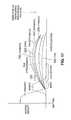
BVCEO/BVCBO≈(1/β)1/m
where m is between about 3 and 6.
| TABLE 1 | |
| BJT REGION | DOPANT DENSITY DERIVED FROM |
| 1 | Triple well/subcollector doping of FIG. 3 |
| 2 | Triple well/subcollector doping plus SIC doping |
| of FIG. 7 | |
| 3 | NPN doping of FIG. 6 |
| 4 | Triple well/subcollector doping plus |
| 5 | NPN doping plus |
| 6 | Triple well/subcollector doping plus NPN doping |
| plus SIC doping | |
Claims (9)
Priority Applications (1)
| Application Number | Priority Date | Filing Date | Title |
|---|---|---|---|
| US13/026,528US8143120B2 (en) | 2004-09-29 | 2011-02-14 | Multiple doping level bipolar junctions transistors and method for forming |
Applications Claiming Priority (5)
| Application Number | Priority Date | Filing Date | Title |
|---|---|---|---|
| US10/953,894US7095094B2 (en) | 2004-09-29 | 2004-09-29 | Multiple doping level bipolar junctions transistors and method for forming |
| US11/458,270US7449388B2 (en) | 2004-09-29 | 2006-07-18 | Method for forming multiple doping level bipolar junctions transistors |
| US12/243,137US7713811B2 (en) | 2004-09-29 | 2008-10-01 | Multiple doping level bipolar junctions transistors and method for forming |
| US12/727,304US7910425B2 (en) | 2004-09-29 | 2010-03-19 | Multiple doping level bipolar junctions transistors and method for forming |
| US13/026,528US8143120B2 (en) | 2004-09-29 | 2011-02-14 | Multiple doping level bipolar junctions transistors and method for forming |
Related Parent Applications (1)
| Application Number | Title | Priority Date | Filing Date |
|---|---|---|---|
| US12/727,304DivisionUS7910425B2 (en) | 2004-09-29 | 2010-03-19 | Multiple doping level bipolar junctions transistors and method for forming |
Publications (2)
| Publication Number | Publication Date |
|---|---|
| US20110133289A1 US20110133289A1 (en) | 2011-06-09 |
| US8143120B2true US8143120B2 (en) | 2012-03-27 |
Family
ID=36098049
Family Applications (5)
| Application Number | Title | Priority Date | Filing Date |
|---|---|---|---|
| US10/953,894Expired - Fee RelatedUS7095094B2 (en) | 2004-09-29 | 2004-09-29 | Multiple doping level bipolar junctions transistors and method for forming |
| US11/458,270Expired - Fee RelatedUS7449388B2 (en) | 2004-09-29 | 2006-07-18 | Method for forming multiple doping level bipolar junctions transistors |
| US12/243,137Expired - LifetimeUS7713811B2 (en) | 2004-09-29 | 2008-10-01 | Multiple doping level bipolar junctions transistors and method for forming |
| US12/727,304Expired - LifetimeUS7910425B2 (en) | 2004-09-29 | 2010-03-19 | Multiple doping level bipolar junctions transistors and method for forming |
| US13/026,528Expired - LifetimeUS8143120B2 (en) | 2004-09-29 | 2011-02-14 | Multiple doping level bipolar junctions transistors and method for forming |
Family Applications Before (4)
| Application Number | Title | Priority Date | Filing Date |
|---|---|---|---|
| US10/953,894Expired - Fee RelatedUS7095094B2 (en) | 2004-09-29 | 2004-09-29 | Multiple doping level bipolar junctions transistors and method for forming |
| US11/458,270Expired - Fee RelatedUS7449388B2 (en) | 2004-09-29 | 2006-07-18 | Method for forming multiple doping level bipolar junctions transistors |
| US12/243,137Expired - LifetimeUS7713811B2 (en) | 2004-09-29 | 2008-10-01 | Multiple doping level bipolar junctions transistors and method for forming |
| US12/727,304Expired - LifetimeUS7910425B2 (en) | 2004-09-29 | 2010-03-19 | Multiple doping level bipolar junctions transistors and method for forming |
Country Status (1)
| Country | Link |
|---|---|
| US (5) | US7095094B2 (en) |
Cited By (52)
| Publication number | Priority date | Publication date | Assignee | Title |
|---|---|---|---|---|
| US20110121404A1 (en)* | 2009-09-30 | 2011-05-26 | Lucian Shifren | Advanced transistors with punch through suppression |
| US8377783B2 (en) | 2010-09-30 | 2013-02-19 | Suvolta, Inc. | Method for reducing punch-through in a transistor device |
| US8400219B2 (en) | 2011-03-24 | 2013-03-19 | Suvolta, Inc. | Analog circuits having improved transistors, and methods therefor |
| US8404551B2 (en) | 2010-12-03 | 2013-03-26 | Suvolta, Inc. | Source/drain extension control for advanced transistors |
| US8461875B1 (en) | 2011-02-18 | 2013-06-11 | Suvolta, Inc. | Digital circuits having improved transistors, and methods therefor |
| US8525271B2 (en) | 2011-03-03 | 2013-09-03 | Suvolta, Inc. | Semiconductor structure with improved channel stack and method for fabrication thereof |
| US8530286B2 (en) | 2010-04-12 | 2013-09-10 | Suvolta, Inc. | Low power semiconductor transistor structure and method of fabrication thereof |
| US8569156B1 (en) | 2011-05-16 | 2013-10-29 | Suvolta, Inc. | Reducing or eliminating pre-amorphization in transistor manufacture |
| US8569128B2 (en) | 2010-06-21 | 2013-10-29 | Suvolta, Inc. | Semiconductor structure and method of fabrication thereof with mixed metal types |
| US8599623B1 (en) | 2011-12-23 | 2013-12-03 | Suvolta, Inc. | Circuits and methods for measuring circuit elements in an integrated circuit device |
| US8614128B1 (en) | 2011-08-23 | 2013-12-24 | Suvolta, Inc. | CMOS structures and processes based on selective thinning |
| US8629016B1 (en) | 2011-07-26 | 2014-01-14 | Suvolta, Inc. | Multiple transistor types formed in a common epitaxial layer by differential out-diffusion from a doped underlayer |
| US8637955B1 (en) | 2012-08-31 | 2014-01-28 | Suvolta, Inc. | Semiconductor structure with reduced junction leakage and method of fabrication thereof |
| US8645878B1 (en) | 2011-08-23 | 2014-02-04 | Suvolta, Inc. | Porting a circuit design from a first semiconductor process to a second semiconductor process |
| US8713511B1 (en) | 2011-09-16 | 2014-04-29 | Suvolta, Inc. | Tools and methods for yield-aware semiconductor manufacturing process target generation |
| US8735987B1 (en) | 2011-06-06 | 2014-05-27 | Suvolta, Inc. | CMOS gate stack structures and processes |
| US8748986B1 (en) | 2011-08-05 | 2014-06-10 | Suvolta, Inc. | Electronic device with controlled threshold voltage |
| US8748270B1 (en) | 2011-03-30 | 2014-06-10 | Suvolta, Inc. | Process for manufacturing an improved analog transistor |
| US8759872B2 (en) | 2010-06-22 | 2014-06-24 | Suvolta, Inc. | Transistor with threshold voltage set notch and method of fabrication thereof |
| US8796048B1 (en) | 2011-05-11 | 2014-08-05 | Suvolta, Inc. | Monitoring and measurement of thin film layers |
| US8811068B1 (en) | 2011-05-13 | 2014-08-19 | Suvolta, Inc. | Integrated circuit devices and methods |
| US8816754B1 (en) | 2012-11-02 | 2014-08-26 | Suvolta, Inc. | Body bias circuits and methods |
| US8819603B1 (en) | 2011-12-15 | 2014-08-26 | Suvolta, Inc. | Memory circuits and methods of making and designing the same |
| US8863064B1 (en) | 2012-03-23 | 2014-10-14 | Suvolta, Inc. | SRAM cell layout structure and devices therefrom |
| US8877619B1 (en) | 2012-01-23 | 2014-11-04 | Suvolta, Inc. | Process for manufacture of integrated circuits with different channel doping transistor architectures and devices therefrom |
| US8883600B1 (en) | 2011-12-22 | 2014-11-11 | Suvolta, Inc. | Transistor having reduced junction leakage and methods of forming thereof |
| US8895327B1 (en) | 2011-12-09 | 2014-11-25 | Suvolta, Inc. | Tipless transistors, short-tip transistors, and methods and circuits therefor |
| US8970289B1 (en) | 2012-01-23 | 2015-03-03 | Suvolta, Inc. | Circuits and devices for generating bi-directional body bias voltages, and methods therefor |
| US8976575B1 (en) | 2013-08-29 | 2015-03-10 | Suvolta, Inc. | SRAM performance monitor |
| US8988153B1 (en) | 2013-03-09 | 2015-03-24 | Suvolta, Inc. | Ring oscillator with NMOS or PMOS variation insensitivity |
| US8994415B1 (en) | 2013-03-01 | 2015-03-31 | Suvolta, Inc. | Multiple VDD clock buffer |
| US8995204B2 (en) | 2011-06-23 | 2015-03-31 | Suvolta, Inc. | Circuit devices and methods having adjustable transistor body bias |
| US8999861B1 (en) | 2011-05-11 | 2015-04-07 | Suvolta, Inc. | Semiconductor structure with substitutional boron and method for fabrication thereof |
| US9041126B2 (en) | 2012-09-21 | 2015-05-26 | Mie Fujitsu Semiconductor Limited | Deeply depleted MOS transistors having a screening layer and methods thereof |
| US9054219B1 (en) | 2011-08-05 | 2015-06-09 | Mie Fujitsu Semiconductor Limited | Semiconductor devices having fin structures and fabrication methods thereof |
| US9070477B1 (en) | 2012-12-12 | 2015-06-30 | Mie Fujitsu Semiconductor Limited | Bit interleaved low voltage static random access memory (SRAM) and related methods |
| US9093550B1 (en) | 2012-01-31 | 2015-07-28 | Mie Fujitsu Semiconductor Limited | Integrated circuits having a plurality of high-K metal gate FETs with various combinations of channel foundation structure and gate stack structure and methods of making same |
| US9093997B1 (en) | 2012-11-15 | 2015-07-28 | Mie Fujitsu Semiconductor Limited | Slew based process and bias monitors and related methods |
| US9112057B1 (en) | 2012-09-18 | 2015-08-18 | Mie Fujitsu Semiconductor Limited | Semiconductor devices with dopant migration suppression and method of fabrication thereof |
| US9112484B1 (en) | 2012-12-20 | 2015-08-18 | Mie Fujitsu Semiconductor Limited | Integrated circuit process and bias monitors and related methods |
| US9112495B1 (en) | 2013-03-15 | 2015-08-18 | Mie Fujitsu Semiconductor Limited | Integrated circuit device body bias circuits and methods |
| US9236466B1 (en) | 2011-10-07 | 2016-01-12 | Mie Fujitsu Semiconductor Limited | Analog circuits having improved insulated gate transistors, and methods therefor |
| US9268885B1 (en) | 2013-02-28 | 2016-02-23 | Mie Fujitsu Semiconductor Limited | Integrated circuit device methods and models with predicted device metric variations |
| US9299801B1 (en) | 2013-03-14 | 2016-03-29 | Mie Fujitsu Semiconductor Limited | Method for fabricating a transistor device with a tuned dopant profile |
| US9299698B2 (en) | 2012-06-27 | 2016-03-29 | Mie Fujitsu Semiconductor Limited | Semiconductor structure with multiple transistors having various threshold voltages |
| US9319013B2 (en) | 2014-08-19 | 2016-04-19 | Mie Fujitsu Semiconductor Limited | Operational amplifier input offset correction with transistor threshold voltage adjustment |
| US9406567B1 (en) | 2012-02-28 | 2016-08-02 | Mie Fujitsu Semiconductor Limited | Method for fabricating multiple transistor devices on a substrate with varying threshold voltages |
| US9431068B2 (en) | 2012-10-31 | 2016-08-30 | Mie Fujitsu Semiconductor Limited | Dynamic random access memory (DRAM) with low variation transistor peripheral circuits |
| US9449967B1 (en) | 2013-03-15 | 2016-09-20 | Fujitsu Semiconductor Limited | Transistor array structure |
| US9478571B1 (en) | 2013-05-24 | 2016-10-25 | Mie Fujitsu Semiconductor Limited | Buried channel deeply depleted channel transistor |
| US9710006B2 (en) | 2014-07-25 | 2017-07-18 | Mie Fujitsu Semiconductor Limited | Power up body bias circuits and methods |
| US10074568B2 (en) | 2009-09-30 | 2018-09-11 | Mie Fujitsu Semiconductor Limited | Electronic devices and systems, and methods for making and using same |
Families Citing this family (17)
| Publication number | Priority date | Publication date | Assignee | Title |
|---|---|---|---|---|
| US7064416B2 (en)* | 2001-11-16 | 2006-06-20 | International Business Machines Corporation | Semiconductor device and method having multiple subcollectors formed on a common wafer |
| US7095094B2 (en)* | 2004-09-29 | 2006-08-22 | Agere Systems Inc. | Multiple doping level bipolar junctions transistors and method for forming |
| US7282771B2 (en)* | 2005-01-25 | 2007-10-16 | International Business Machines Corporation | Structure and method for latchup suppression |
| US7439119B2 (en)* | 2006-02-24 | 2008-10-21 | Agere Systems Inc. | Thermally stable BiCMOS fabrication method and bipolar junction transistors formed according to the method |
| KR101108711B1 (en) | 2007-08-23 | 2012-01-30 | 삼성전자주식회사 | An active pattern structure, a method of forming the same, a nonvolatile memory device and a method of manufacturing the same. |
| US20100009507A1 (en)* | 2008-07-10 | 2010-01-14 | Krutsick Thomas J | Method of constructing cmos device tubs |
| JP5562628B2 (en)* | 2009-12-21 | 2014-07-30 | ラピスセミコンダクタ株式会社 | Manufacturing method of semiconductor device |
| US8501572B2 (en)* | 2010-09-02 | 2013-08-06 | Taiwan Semiconductor Manufacturing Company, Ltd. | Spacer structure for transistor device and method of manufacturing same |
| US8552500B2 (en) | 2011-05-24 | 2013-10-08 | International Business Machines Corporation | Structure for CMOS ETSOI with multiple threshold voltages and active well bias capability |
| US8415743B2 (en) | 2011-05-24 | 2013-04-09 | International Business Machines Corporation | ETSOI CMOS with back gates |
| US20160169833A1 (en) | 2014-12-11 | 2016-06-16 | International Business Machines Corporation | Biosensor based on heterojunction bipolar transistor |
| US9831328B2 (en)* | 2015-02-12 | 2017-11-28 | Taiwan Semiconductor Manufacturing Co., Ltd. | Bipolar junction transistor (BJT) base conductor pullback |
| US9711516B2 (en)* | 2015-10-30 | 2017-07-18 | Taiwan Semiconductor Manufacturing Company Ltd. | Non-volatile memory having a gate-layered triple well structure |
| US11355585B2 (en) | 2019-10-01 | 2022-06-07 | Analog Devices International Unlimited Company | Bipolar junction transistor, and a method of forming a charge control structure for a bipolar junction transistor |
| US11563084B2 (en)* | 2019-10-01 | 2023-01-24 | Analog Devices International Unlimited Company | Bipolar junction transistor, and a method of forming an emitter for a bipolar junction transistor |
| US11404540B2 (en) | 2019-10-01 | 2022-08-02 | Analog Devices International Unlimited Company | Bipolar junction transistor, and a method of forming a collector for a bipolar junction transistor |
| US11777018B2 (en)* | 2020-11-19 | 2023-10-03 | Ideal Power Inc. | Layout to reduce current crowding at endpoints |
Citations (16)
| Publication number | Priority date | Publication date | Assignee | Title |
|---|---|---|---|---|
| US4881105A (en) | 1988-06-13 | 1989-11-14 | International Business Machines Corporation | Integrated trench-transistor structure and fabrication process |
| US5079613A (en) | 1987-07-10 | 1992-01-07 | Kabushiki Kaisha Toshiba | Semiconductor device having different impurity concentration wells |
| US5497023A (en) | 1985-09-25 | 1996-03-05 | Hitachi, Ltd. | Semiconductor memory device having separately biased wells for isolation |
| US5990535A (en) | 1995-06-30 | 1999-11-23 | Sgs-Thomson Microelectronics, S.R.L. | Power integrated circuit |
| US6266222B1 (en) | 1997-12-31 | 2001-07-24 | Stmicroelectronics S.R.L. | ESD protection network for circuit structures formed in a semiconductor |
| US6285240B1 (en) | 1999-01-14 | 2001-09-04 | Macronix International Co., Ltd. | Low threshold MOS two phase negative charge pump |
| US6525394B1 (en) | 2000-08-03 | 2003-02-25 | Ray E. Kuhn | Substrate isolation for analog/digital IC chips |
| US6586297B1 (en) | 2002-06-01 | 2003-07-01 | Newport Fab, Llc | Method for integrating a metastable base into a high-performance HBT and related structure |
| US6600186B1 (en) | 1998-11-19 | 2003-07-29 | Taiwan Semiconductor Manufacturing Company | Process technology architecture of embedded DRAM |
| US6746928B1 (en) | 2001-05-08 | 2004-06-08 | Newport Fab, Llc | Method for opening a semiconductor region for fabricating an HBT |
| US20040164354A1 (en) | 2001-06-14 | 2004-08-26 | Sarnoff Corporation | Minimum-dimension, fully- silicided MOS driver and ESD protection design for optimized inter-finger coupling |
| US6803634B2 (en)* | 2001-11-07 | 2004-10-12 | Denso Corporation | Stabilization in device characteristics of a bipolar transistor that is included in a semiconductor device with a CMOSFET |
| US6808973B2 (en)* | 2002-01-31 | 2004-10-26 | Renesas Technology Corp. | Manufacturing method of semiconductor device |
| US6831334B2 (en) | 2000-05-31 | 2004-12-14 | Seiko Epson Corporation | Semiconductor device having electrostatic protection circuit and method of fabricating the same |
| US20060065936A1 (en) | 2004-09-29 | 2006-03-30 | Kerr Daniel C | Multiple doping level bipolar junctions transistors and method for forming |
| US7186610B1 (en)* | 2004-08-13 | 2007-03-06 | Altera Corporation | ESD protection device for high performance IC |
Family Cites Families (1)
| Publication number | Priority date | Publication date | Assignee | Title |
|---|---|---|---|---|
| US674928A (en)* | 1900-03-22 | 1901-05-28 | Castner Electrolytic Alkali Company | Pipe-coupling. |
- 2004
- 2004-09-29USUS10/953,894patent/US7095094B2/ennot_activeExpired - Fee Related
- 2006
- 2006-07-18USUS11/458,270patent/US7449388B2/ennot_activeExpired - Fee Related
- 2008
- 2008-10-01USUS12/243,137patent/US7713811B2/ennot_activeExpired - Lifetime
- 2010
- 2010-03-19USUS12/727,304patent/US7910425B2/ennot_activeExpired - Lifetime
- 2011
- 2011-02-14USUS13/026,528patent/US8143120B2/ennot_activeExpired - Lifetime
Patent Citations (21)
| Publication number | Priority date | Publication date | Assignee | Title |
|---|---|---|---|---|
| US5497023A (en) | 1985-09-25 | 1996-03-05 | Hitachi, Ltd. | Semiconductor memory device having separately biased wells for isolation |
| US5079613A (en) | 1987-07-10 | 1992-01-07 | Kabushiki Kaisha Toshiba | Semiconductor device having different impurity concentration wells |
| US4881105A (en) | 1988-06-13 | 1989-11-14 | International Business Machines Corporation | Integrated trench-transistor structure and fabrication process |
| US5990535A (en) | 1995-06-30 | 1999-11-23 | Sgs-Thomson Microelectronics, S.R.L. | Power integrated circuit |
| US6266222B1 (en) | 1997-12-31 | 2001-07-24 | Stmicroelectronics S.R.L. | ESD protection network for circuit structures formed in a semiconductor |
| US6600186B1 (en) | 1998-11-19 | 2003-07-29 | Taiwan Semiconductor Manufacturing Company | Process technology architecture of embedded DRAM |
| US6285240B1 (en) | 1999-01-14 | 2001-09-04 | Macronix International Co., Ltd. | Low threshold MOS two phase negative charge pump |
| US6831334B2 (en) | 2000-05-31 | 2004-12-14 | Seiko Epson Corporation | Semiconductor device having electrostatic protection circuit and method of fabricating the same |
| US6525394B1 (en) | 2000-08-03 | 2003-02-25 | Ray E. Kuhn | Substrate isolation for analog/digital IC chips |
| US6746928B1 (en) | 2001-05-08 | 2004-06-08 | Newport Fab, Llc | Method for opening a semiconductor region for fabricating an HBT |
| US20040164354A1 (en) | 2001-06-14 | 2004-08-26 | Sarnoff Corporation | Minimum-dimension, fully- silicided MOS driver and ESD protection design for optimized inter-finger coupling |
| US6803634B2 (en)* | 2001-11-07 | 2004-10-12 | Denso Corporation | Stabilization in device characteristics of a bipolar transistor that is included in a semiconductor device with a CMOSFET |
| US6808973B2 (en)* | 2002-01-31 | 2004-10-26 | Renesas Technology Corp. | Manufacturing method of semiconductor device |
| US6586297B1 (en) | 2002-06-01 | 2003-07-01 | Newport Fab, Llc | Method for integrating a metastable base into a high-performance HBT and related structure |
| US7186610B1 (en)* | 2004-08-13 | 2007-03-06 | Altera Corporation | ESD protection device for high performance IC |
| US20060065936A1 (en) | 2004-09-29 | 2006-03-30 | Kerr Daniel C | Multiple doping level bipolar junctions transistors and method for forming |
| US7095094B2 (en) | 2004-09-29 | 2006-08-22 | Agere Systems Inc. | Multiple doping level bipolar junctions transistors and method for forming |
| US20060252215A1 (en)* | 2004-09-29 | 2006-11-09 | Kerr Daniel C | Multiple doping level bipolar junctions transistors and method for forming |
| US7449388B2 (en) | 2004-09-29 | 2008-11-11 | Agere Systems Inc. | Method for forming multiple doping level bipolar junctions transistors |
| US7713811B2 (en) | 2004-09-29 | 2010-05-11 | Agere Systems Inc. | Multiple doping level bipolar junctions transistors and method for forming |
| US20100173459A1 (en) | 2004-09-29 | 2010-07-08 | Agere Systems Inc. | Multiple doping level bipolar junctions transistors and method for forming |
Cited By (114)
| Publication number | Priority date | Publication date | Assignee | Title |
|---|---|---|---|---|
| US11887895B2 (en) | 2009-09-30 | 2024-01-30 | United Semiconductor Japan Co., Ltd. | Electronic devices and systems, and methods for making and using the same |
| US10074568B2 (en) | 2009-09-30 | 2018-09-11 | Mie Fujitsu Semiconductor Limited | Electronic devices and systems, and methods for making and using same |
| US10217668B2 (en) | 2009-09-30 | 2019-02-26 | Mie Fujitsu Semiconductor Limited | Electronic devices and systems, and methods for making and using the same |
| US10224244B2 (en) | 2009-09-30 | 2019-03-05 | Mie Fujitsu Semiconductor Limited | Electronic devices and systems, and methods for making and using the same |
| US8421162B2 (en) | 2009-09-30 | 2013-04-16 | Suvolta, Inc. | Advanced transistors with punch through suppression |
| US10325986B2 (en) | 2009-09-30 | 2019-06-18 | Mie Fujitsu Semiconductor Limited | Advanced transistors with punch through suppression |
| US20110121404A1 (en)* | 2009-09-30 | 2011-05-26 | Lucian Shifren | Advanced transistors with punch through suppression |
| US11062950B2 (en) | 2009-09-30 | 2021-07-13 | United Semiconductor Japan Co., Ltd. | Electronic devices and systems, and methods for making and using the same |
| US9263523B2 (en) | 2009-09-30 | 2016-02-16 | Mie Fujitsu Semiconductor Limited | Advanced transistors with punch through suppression |
| US9508800B2 (en) | 2009-09-30 | 2016-11-29 | Mie Fujitsu Semiconductor Limited | Advanced transistors with punch through suppression |
| US9496261B2 (en) | 2010-04-12 | 2016-11-15 | Mie Fujitsu Semiconductor Limited | Low power semiconductor transistor structure and method of fabrication thereof |
| US9865596B2 (en) | 2010-04-12 | 2018-01-09 | Mie Fujitsu Semiconductor Limited | Low power semiconductor transistor structure and method of fabrication thereof |
| US8530286B2 (en) | 2010-04-12 | 2013-09-10 | Suvolta, Inc. | Low power semiconductor transistor structure and method of fabrication thereof |
| US8569128B2 (en) | 2010-06-21 | 2013-10-29 | Suvolta, Inc. | Semiconductor structure and method of fabrication thereof with mixed metal types |
| US9224733B2 (en) | 2010-06-21 | 2015-12-29 | Mie Fujitsu Semiconductor Limited | Semiconductor structure and method of fabrication thereof with mixed metal types |
| US8759872B2 (en) | 2010-06-22 | 2014-06-24 | Suvolta, Inc. | Transistor with threshold voltage set notch and method of fabrication thereof |
| US9418987B2 (en) | 2010-06-22 | 2016-08-16 | Mie Fujitsu Semiconductor Limited | Transistor with threshold voltage set notch and method of fabrication thereof |
| US9922977B2 (en) | 2010-06-22 | 2018-03-20 | Mie Fujitsu Semiconductor Limited | Transistor with threshold voltage set notch and method of fabrication thereof |
| US8377783B2 (en) | 2010-09-30 | 2013-02-19 | Suvolta, Inc. | Method for reducing punch-through in a transistor device |
| US8686511B2 (en) | 2010-12-03 | 2014-04-01 | Suvolta, Inc. | Source/drain extension control for advanced transistors |
| US8563384B2 (en) | 2010-12-03 | 2013-10-22 | Suvolta, Inc. | Source/drain extension control for advanced transistors |
| US9006843B2 (en) | 2010-12-03 | 2015-04-14 | Suvolta, Inc. | Source/drain extension control for advanced transistors |
| US8404551B2 (en) | 2010-12-03 | 2013-03-26 | Suvolta, Inc. | Source/drain extension control for advanced transistors |
| US9184750B1 (en) | 2011-02-18 | 2015-11-10 | Mie Fujitsu Semiconductor Limited | Digital circuits having improved transistors, and methods therefor |
| US9838012B2 (en) | 2011-02-18 | 2017-12-05 | Mie Fujitsu Semiconductor Limited | Digital circuits having improved transistors, and methods therefor |
| US9680470B2 (en) | 2011-02-18 | 2017-06-13 | Mie Fujitsu Semiconductor Limited | Digital circuits having improved transistors, and methods therefor |
| US8461875B1 (en) | 2011-02-18 | 2013-06-11 | Suvolta, Inc. | Digital circuits having improved transistors, and methods therefor |
| US10250257B2 (en) | 2011-02-18 | 2019-04-02 | Mie Fujitsu Semiconductor Limited | Digital circuits having improved transistors, and methods therefor |
| US9985631B2 (en) | 2011-02-18 | 2018-05-29 | Mie Fujitsu Semiconductor Limited | Digital circuits having improved transistors, and methods therefor |
| US9111785B2 (en) | 2011-03-03 | 2015-08-18 | Mie Fujitsu Semiconductor Limited | Semiconductor structure with improved channel stack and method for fabrication thereof |
| US8525271B2 (en) | 2011-03-03 | 2013-09-03 | Suvolta, Inc. | Semiconductor structure with improved channel stack and method for fabrication thereof |
| US8847684B2 (en) | 2011-03-24 | 2014-09-30 | Suvolta, Inc. | Analog circuits having improved transistors, and methods therefor |
| US9231541B2 (en) | 2011-03-24 | 2016-01-05 | Mie Fujitsu Semiconductor Limited | Analog circuits having improved transistors, and methods therefor |
| US8400219B2 (en) | 2011-03-24 | 2013-03-19 | Suvolta, Inc. | Analog circuits having improved transistors, and methods therefor |
| US8748270B1 (en) | 2011-03-30 | 2014-06-10 | Suvolta, Inc. | Process for manufacturing an improved analog transistor |
| US9093469B2 (en) | 2011-03-30 | 2015-07-28 | Mie Fujitsu Semiconductor Limited | Analog transistor |
| US8796048B1 (en) | 2011-05-11 | 2014-08-05 | Suvolta, Inc. | Monitoring and measurement of thin film layers |
| US8999861B1 (en) | 2011-05-11 | 2015-04-07 | Suvolta, Inc. | Semiconductor structure with substitutional boron and method for fabrication thereof |
| US8811068B1 (en) | 2011-05-13 | 2014-08-19 | Suvolta, Inc. | Integrated circuit devices and methods |
| US9362291B1 (en) | 2011-05-13 | 2016-06-07 | Mie Fujitsu Semiconductor Limited | Integrated circuit devices and methods |
| US9966130B2 (en) | 2011-05-13 | 2018-05-08 | Mie Fujitsu Semiconductor Limited | Integrated circuit devices and methods |
| US9741428B2 (en) | 2011-05-13 | 2017-08-22 | Mie Fujitsu Semiconductor Limited | Integrated circuit devices and methods |
| US9793172B2 (en) | 2011-05-16 | 2017-10-17 | Mie Fujitsu Semiconductor Limited | Reducing or eliminating pre-amorphization in transistor manufacture |
| US8569156B1 (en) | 2011-05-16 | 2013-10-29 | Suvolta, Inc. | Reducing or eliminating pre-amorphization in transistor manufacture |
| US9514940B2 (en) | 2011-05-16 | 2016-12-06 | Mie Fujitsu Semiconductor Limited | Reducing or eliminating pre-amorphization in transistor manufacture |
| US8937005B2 (en) | 2011-05-16 | 2015-01-20 | Suvolta, Inc. | Reducing or eliminating pre-amorphization in transistor manufacture |
| US9281248B1 (en) | 2011-06-06 | 2016-03-08 | Mie Fujitsu Semiconductor Limited | CMOS gate stack structures and processes |
| US9508728B2 (en) | 2011-06-06 | 2016-11-29 | Mie Fujitsu Semiconductor Limited | CMOS gate stack structures and processes |
| US8735987B1 (en) | 2011-06-06 | 2014-05-27 | Suvolta, Inc. | CMOS gate stack structures and processes |
| US8995204B2 (en) | 2011-06-23 | 2015-03-31 | Suvolta, Inc. | Circuit devices and methods having adjustable transistor body bias |
| US8653604B1 (en) | 2011-07-26 | 2014-02-18 | Suvolta, Inc. | Multiple transistor types formed in a common epitaxial layer by differential out-diffusion from a doped underlayer |
| US8916937B1 (en) | 2011-07-26 | 2014-12-23 | Suvolta, Inc. | Multiple transistor types formed in a common epitaxial layer by differential out-diffusion from a doped underlayer |
| US8629016B1 (en) | 2011-07-26 | 2014-01-14 | Suvolta, Inc. | Multiple transistor types formed in a common epitaxial layer by differential out-diffusion from a doped underlayer |
| US9054219B1 (en) | 2011-08-05 | 2015-06-09 | Mie Fujitsu Semiconductor Limited | Semiconductor devices having fin structures and fabrication methods thereof |
| US8963249B1 (en) | 2011-08-05 | 2015-02-24 | Suvolta, Inc. | Electronic device with controlled threshold voltage |
| US8748986B1 (en) | 2011-08-05 | 2014-06-10 | Suvolta, Inc. | Electronic device with controlled threshold voltage |
| US8645878B1 (en) | 2011-08-23 | 2014-02-04 | Suvolta, Inc. | Porting a circuit design from a first semiconductor process to a second semiconductor process |
| US8806395B1 (en) | 2011-08-23 | 2014-08-12 | Suvolta, Inc. | Porting a circuit design from a first semiconductor process to a second semiconductor process |
| US9117746B1 (en) | 2011-08-23 | 2015-08-25 | Mie Fujitsu Semiconductor Limited | Porting a circuit design from a first semiconductor process to a second semiconductor process |
| US8614128B1 (en) | 2011-08-23 | 2013-12-24 | Suvolta, Inc. | CMOS structures and processes based on selective thinning |
| US9391076B1 (en) | 2011-08-23 | 2016-07-12 | Mie Fujitsu Semiconductor Limited | CMOS structures and processes based on selective thinning |
| US8713511B1 (en) | 2011-09-16 | 2014-04-29 | Suvolta, Inc. | Tools and methods for yield-aware semiconductor manufacturing process target generation |
| US9236466B1 (en) | 2011-10-07 | 2016-01-12 | Mie Fujitsu Semiconductor Limited | Analog circuits having improved insulated gate transistors, and methods therefor |
| US8895327B1 (en) | 2011-12-09 | 2014-11-25 | Suvolta, Inc. | Tipless transistors, short-tip transistors, and methods and circuits therefor |
| US10573644B2 (en) | 2011-12-09 | 2020-02-25 | Mie Fujitsu Semiconductor Limited | Tipless transistors, short-tip transistors, and methods and circuits therefor |
| US9583484B2 (en) | 2011-12-09 | 2017-02-28 | Mie Fujitsu Semiconductor Limited | Tipless transistors, short-tip transistors, and methods and circuits therefor |
| US9953974B2 (en) | 2011-12-09 | 2018-04-24 | Mie Fujitsu Semiconductor Limited | Tipless transistors, short-tip transistors, and methods and circuits therefor |
| US11145647B2 (en) | 2011-12-09 | 2021-10-12 | United Semiconductor Japan Co., Ltd. | Tipless transistors, short-tip transistors, and methods and circuits therefor |
| US9385121B1 (en) | 2011-12-09 | 2016-07-05 | Mie Fujitsu Semiconductor Limited | Tipless transistors, short-tip transistors, and methods and circuits therefor |
| US8819603B1 (en) | 2011-12-15 | 2014-08-26 | Suvolta, Inc. | Memory circuits and methods of making and designing the same |
| US9196727B2 (en) | 2011-12-22 | 2015-11-24 | Mie Fujitsu Semiconductor Limited | High uniformity screen and epitaxial layers for CMOS devices |
| US9368624B2 (en) | 2011-12-22 | 2016-06-14 | Mie Fujitsu Semiconductor Limited | Method for fabricating a transistor with reduced junction leakage current |
| US8883600B1 (en) | 2011-12-22 | 2014-11-11 | Suvolta, Inc. | Transistor having reduced junction leakage and methods of forming thereof |
| US8599623B1 (en) | 2011-12-23 | 2013-12-03 | Suvolta, Inc. | Circuits and methods for measuring circuit elements in an integrated circuit device |
| US9297850B1 (en) | 2011-12-23 | 2016-03-29 | Mie Fujitsu Semiconductor Limited | Circuits and methods for measuring circuit elements in an integrated circuit device |
| US8877619B1 (en) | 2012-01-23 | 2014-11-04 | Suvolta, Inc. | Process for manufacture of integrated circuits with different channel doping transistor architectures and devices therefrom |
| US8970289B1 (en) | 2012-01-23 | 2015-03-03 | Suvolta, Inc. | Circuits and devices for generating bi-directional body bias voltages, and methods therefor |
| US9385047B2 (en) | 2012-01-31 | 2016-07-05 | Mie Fujitsu Semiconductor Limited | Integrated circuits having a plurality of high-K metal gate FETs with various combinations of channel foundation structure and gate stack structure and methods of making same |
| US9093550B1 (en) | 2012-01-31 | 2015-07-28 | Mie Fujitsu Semiconductor Limited | Integrated circuits having a plurality of high-K metal gate FETs with various combinations of channel foundation structure and gate stack structure and methods of making same |
| US9406567B1 (en) | 2012-02-28 | 2016-08-02 | Mie Fujitsu Semiconductor Limited | Method for fabricating multiple transistor devices on a substrate with varying threshold voltages |
| US8863064B1 (en) | 2012-03-23 | 2014-10-14 | Suvolta, Inc. | SRAM cell layout structure and devices therefrom |
| US9424385B1 (en) | 2012-03-23 | 2016-08-23 | Mie Fujitsu Semiconductor Limited | SRAM cell layout structure and devices therefrom |
| US10014387B2 (en) | 2012-06-27 | 2018-07-03 | Mie Fujitsu Semiconductor Limited | Semiconductor structure with multiple transistors having various threshold voltages |
| US10217838B2 (en) | 2012-06-27 | 2019-02-26 | Mie Fujitsu Semiconductor Limited | Semiconductor structure with multiple transistors having various threshold voltages |
| US9812550B2 (en) | 2012-06-27 | 2017-11-07 | Mie Fujitsu Semiconductor Limited | Semiconductor structure with multiple transistors having various threshold voltages |
| US9299698B2 (en) | 2012-06-27 | 2016-03-29 | Mie Fujitsu Semiconductor Limited | Semiconductor structure with multiple transistors having various threshold voltages |
| US9105711B2 (en) | 2012-08-31 | 2015-08-11 | Mie Fujitsu Semiconductor Limited | Semiconductor structure with reduced junction leakage and method of fabrication thereof |
| US8637955B1 (en) | 2012-08-31 | 2014-01-28 | Suvolta, Inc. | Semiconductor structure with reduced junction leakage and method of fabrication thereof |
| US9112057B1 (en) | 2012-09-18 | 2015-08-18 | Mie Fujitsu Semiconductor Limited | Semiconductor devices with dopant migration suppression and method of fabrication thereof |
| US9041126B2 (en) | 2012-09-21 | 2015-05-26 | Mie Fujitsu Semiconductor Limited | Deeply depleted MOS transistors having a screening layer and methods thereof |
| US9431068B2 (en) | 2012-10-31 | 2016-08-30 | Mie Fujitsu Semiconductor Limited | Dynamic random access memory (DRAM) with low variation transistor peripheral circuits |
| US8816754B1 (en) | 2012-11-02 | 2014-08-26 | Suvolta, Inc. | Body bias circuits and methods |
| US9154123B1 (en) | 2012-11-02 | 2015-10-06 | Mie Fujitsu Semiconductor Limited | Body bias circuits and methods |
| US9319034B2 (en) | 2012-11-15 | 2016-04-19 | Mie Fujitsu Semiconductor Limited | Slew based process and bias monitors and related methods |
| US9093997B1 (en) | 2012-11-15 | 2015-07-28 | Mie Fujitsu Semiconductor Limited | Slew based process and bias monitors and related methods |
| US9070477B1 (en) | 2012-12-12 | 2015-06-30 | Mie Fujitsu Semiconductor Limited | Bit interleaved low voltage static random access memory (SRAM) and related methods |
| US9112484B1 (en) | 2012-12-20 | 2015-08-18 | Mie Fujitsu Semiconductor Limited | Integrated circuit process and bias monitors and related methods |
| US9276561B2 (en) | 2012-12-20 | 2016-03-01 | Mie Fujitsu Semiconductor Limited | Integrated circuit process and bias monitors and related methods |
| US9268885B1 (en) | 2013-02-28 | 2016-02-23 | Mie Fujitsu Semiconductor Limited | Integrated circuit device methods and models with predicted device metric variations |
| US8994415B1 (en) | 2013-03-01 | 2015-03-31 | Suvolta, Inc. | Multiple VDD clock buffer |
| US8988153B1 (en) | 2013-03-09 | 2015-03-24 | Suvolta, Inc. | Ring oscillator with NMOS or PMOS variation insensitivity |
| US9893148B2 (en) | 2013-03-14 | 2018-02-13 | Mie Fujitsu Semiconductor Limited | Method for fabricating a transistor device with a tuned dopant profile |
| US9577041B2 (en) | 2013-03-14 | 2017-02-21 | Mie Fujitsu Semiconductor Limited | Method for fabricating a transistor device with a tuned dopant profile |
| US9299801B1 (en) | 2013-03-14 | 2016-03-29 | Mie Fujitsu Semiconductor Limited | Method for fabricating a transistor device with a tuned dopant profile |
| US9449967B1 (en) | 2013-03-15 | 2016-09-20 | Fujitsu Semiconductor Limited | Transistor array structure |
| US9853019B2 (en) | 2013-03-15 | 2017-12-26 | Mie Fujitsu Semiconductor Limited | Integrated circuit device body bias circuits and methods |
| US9112495B1 (en) | 2013-03-15 | 2015-08-18 | Mie Fujitsu Semiconductor Limited | Integrated circuit device body bias circuits and methods |
| US9548086B2 (en) | 2013-03-15 | 2017-01-17 | Mie Fujitsu Semiconductor Limited | Integrated circuit device body bias circuits and methods |
| US9478571B1 (en) | 2013-05-24 | 2016-10-25 | Mie Fujitsu Semiconductor Limited | Buried channel deeply depleted channel transistor |
| US9786703B2 (en) | 2013-05-24 | 2017-10-10 | Mie Fujitsu Semiconductor Limited | Buried channel deeply depleted channel transistor |
| US9991300B2 (en) | 2013-05-24 | 2018-06-05 | Mie Fujitsu Semiconductor Limited | Buried channel deeply depleted channel transistor |
| US8976575B1 (en) | 2013-08-29 | 2015-03-10 | Suvolta, Inc. | SRAM performance monitor |
| US9710006B2 (en) | 2014-07-25 | 2017-07-18 | Mie Fujitsu Semiconductor Limited | Power up body bias circuits and methods |
| US9319013B2 (en) | 2014-08-19 | 2016-04-19 | Mie Fujitsu Semiconductor Limited | Operational amplifier input offset correction with transistor threshold voltage adjustment |
Also Published As
| Publication number | Publication date |
|---|---|
| US7095094B2 (en) | 2006-08-22 |
| US20060065936A1 (en) | 2006-03-30 |
| US20090029510A1 (en) | 2009-01-29 |
| US7713811B2 (en) | 2010-05-11 |
| US7449388B2 (en) | 2008-11-11 |
| US20060252215A1 (en) | 2006-11-09 |
| US7910425B2 (en) | 2011-03-22 |
| US20100173459A1 (en) | 2010-07-08 |
| US20110133289A1 (en) | 2011-06-09 |
Similar Documents
| Publication | Publication Date | Title |
|---|---|---|
| US8143120B2 (en) | Multiple doping level bipolar junctions transistors and method for forming | |
| EP0375585B1 (en) | Method for manufacturing a BI-CMOS device | |
| US6445044B2 (en) | Apparatus improving latchup immunity in a dual-polysilicon gate | |
| US5248624A (en) | Method of making isolated vertical pnp transistor in a complementary bicmos process with eeprom memory | |
| US5329147A (en) | High voltage integrated flyback circuit in 2 μm CMOS | |
| US5438005A (en) | Deep collection guard ring | |
| US6861303B2 (en) | JFET structure for integrated circuit and fabrication method | |
| US6949424B2 (en) | Single poly-emitter PNP using DWELL diffusion in a BiCMOS technology | |
| US6030864A (en) | Vertical NPN transistor for 0.35 micrometer node CMOS logic technology | |
| US11990466B2 (en) | High voltage electrostatic devices | |
| US7217609B2 (en) | Semiconductor fabrication process, lateral PNP transistor, and integrated circuit | |
| JPH01155653A (en) | High voltage incorporating bipolar/cmos integrated circuit | |
| US6071763A (en) | Method of fabricating layered integrated circuit | |
| US5538908A (en) | Method for manufacturing a BiCMOS semiconductor device | |
| US20010009290A1 (en) | Buried guard rings and method for forming the same | |
| US6987039B2 (en) | Forming lateral bipolar junction transistor in CMOS flow | |
| US6303420B1 (en) | Integrated bipolar junction transistor for mixed signal circuits | |
| US5624856A (en) | Method for forming a lateral bipolar transistor | |
| US5493149A (en) | Transistor device with increased breakdown voltage | |
| US5124775A (en) | Semiconductor device with oxide sidewall | |
| US6011283A (en) | Pillar emitter for BiCMOS devices | |
| US20090159984A1 (en) | Semiconductor Device and Method for Manufacturing the Same | |
| US6337252B1 (en) | Semiconductor device manufacturing method | |
| WO2003043080A1 (en) | Lateral pnp transistor device, integrated circuit, and fabrication process thereof | |
| KR19980086423A (en) | Combined MOS / Bipolar Transistors |
Legal Events
| Date | Code | Title | Description |
|---|---|---|---|
| AS | Assignment | Owner name:AGERE SYSTEMS INC., PENNSYLVANIA Free format text:ASSIGNMENT OF ASSIGNORS INTEREST;ASSIGNORS:KERR, DANIEL CHARLES;CARROLL, MICHAEL SCOTT;HAMAD, AMAL MA;AND OTHERS;SIGNING DATES FROM 20041115 TO 20050106;REEL/FRAME:025803/0049 | |
| STCF | Information on status: patent grant | Free format text:PATENTED CASE | |
| AS | Assignment | Owner name:DEUTSCHE BANK AG NEW YORK BRANCH, AS COLLATERAL AG Free format text:PATENT SECURITY AGREEMENT;ASSIGNORS:LSI CORPORATION;AGERE SYSTEMS LLC;REEL/FRAME:032856/0031 Effective date:20140506 | |
| AS | Assignment | Owner name:AVAGO TECHNOLOGIES GENERAL IP (SINGAPORE) PTE. LTD Free format text:ASSIGNMENT OF ASSIGNORS INTEREST;ASSIGNOR:AGERE SYSTEMS LLC;REEL/FRAME:035365/0634 Effective date:20140804 | |
| FPAY | Fee payment | Year of fee payment:4 | |
| AS | Assignment | Owner name:LSI CORPORATION, CALIFORNIA Free format text:TERMINATION AND RELEASE OF SECURITY INTEREST IN PATENT RIGHTS (RELEASES RF 032856-0031);ASSIGNOR:DEUTSCHE BANK AG NEW YORK BRANCH, AS COLLATERAL AGENT;REEL/FRAME:037684/0039 Effective date:20160201 Owner name:AGERE SYSTEMS LLC, PENNSYLVANIA Free format text:TERMINATION AND RELEASE OF SECURITY INTEREST IN PATENT RIGHTS (RELEASES RF 032856-0031);ASSIGNOR:DEUTSCHE BANK AG NEW YORK BRANCH, AS COLLATERAL AGENT;REEL/FRAME:037684/0039 Effective date:20160201 | |
| AS | Assignment | Owner name:BANK OF AMERICA, N.A., AS COLLATERAL AGENT, NORTH CAROLINA Free format text:PATENT SECURITY AGREEMENT;ASSIGNOR:AVAGO TECHNOLOGIES GENERAL IP (SINGAPORE) PTE. LTD.;REEL/FRAME:037808/0001 Effective date:20160201 Owner name:BANK OF AMERICA, N.A., AS COLLATERAL AGENT, NORTH Free format text:PATENT SECURITY AGREEMENT;ASSIGNOR:AVAGO TECHNOLOGIES GENERAL IP (SINGAPORE) PTE. LTD.;REEL/FRAME:037808/0001 Effective date:20160201 | |
| AS | Assignment | Owner name:AVAGO TECHNOLOGIES GENERAL IP (SINGAPORE) PTE. LTD., SINGAPORE Free format text:TERMINATION AND RELEASE OF SECURITY INTEREST IN PATENTS;ASSIGNOR:BANK OF AMERICA, N.A., AS COLLATERAL AGENT;REEL/FRAME:041710/0001 Effective date:20170119 Owner name:AVAGO TECHNOLOGIES GENERAL IP (SINGAPORE) PTE. LTD Free format text:TERMINATION AND RELEASE OF SECURITY INTEREST IN PATENTS;ASSIGNOR:BANK OF AMERICA, N.A., AS COLLATERAL AGENT;REEL/FRAME:041710/0001 Effective date:20170119 | |
| AS | Assignment | Owner name:BELL SEMICONDUCTOR, LLC, ILLINOIS Free format text:ASSIGNMENT OF ASSIGNORS INTEREST;ASSIGNORS:AVAGO TECHNOLOGIES GENERAL IP (SINGAPORE) PTE. LTD.;BROADCOM CORPORATION;REEL/FRAME:044886/0001 Effective date:20171208 Owner name:BELL SEMICONDUCTOR, LLC, ILLINOIS Free format text:ASSIGNMENT OF ASSIGNORS INTEREST;ASSIGNORS:AVAGO TECHNOLOGIES GENERAL IP (SINGAPORE) PTE. LTD.;BROADCOM CORPORATION;REEL/FRAME:044886/0608 Effective date:20171208 | |
| AS | Assignment | Owner name:CORTLAND CAPITAL MARKET SERVICES LLC, AS COLLATERA Free format text:SECURITY INTEREST;ASSIGNORS:HILCO PATENT ACQUISITION 56, LLC;BELL SEMICONDUCTOR, LLC;BELL NORTHERN RESEARCH, LLC;REEL/FRAME:045216/0020 Effective date:20180124 | |
| MAFP | Maintenance fee payment | Free format text:PAYMENT OF MAINTENANCE FEE, 8TH YEAR, LARGE ENTITY (ORIGINAL EVENT CODE: M1552); ENTITY STATUS OF PATENT OWNER: LARGE ENTITY Year of fee payment:8 | |
| AS | Assignment | Owner name:BELL NORTHERN RESEARCH, LLC, ILLINOIS Free format text:SECURITY INTEREST;ASSIGNOR:CORTLAND CAPITAL MARKET SERVICES LLC;REEL/FRAME:060885/0001 Effective date:20220401 Owner name:BELL SEMICONDUCTOR, LLC, ILLINOIS Free format text:SECURITY INTEREST;ASSIGNOR:CORTLAND CAPITAL MARKET SERVICES LLC;REEL/FRAME:060885/0001 Effective date:20220401 Owner name:HILCO PATENT ACQUISITION 56, LLC, ILLINOIS Free format text:SECURITY INTEREST;ASSIGNOR:CORTLAND CAPITAL MARKET SERVICES LLC;REEL/FRAME:060885/0001 Effective date:20220401 Owner name:BELL NORTHERN RESEARCH, LLC, ILLINOIS Free format text:RELEASE BY SECURED PARTY;ASSIGNOR:CORTLAND CAPITAL MARKET SERVICES LLC;REEL/FRAME:059720/0719 Effective date:20220401 Owner name:BELL SEMICONDUCTOR, LLC, ILLINOIS Free format text:RELEASE BY SECURED PARTY;ASSIGNOR:CORTLAND CAPITAL MARKET SERVICES LLC;REEL/FRAME:059720/0719 Effective date:20220401 Owner name:HILCO PATENT ACQUISITION 56, LLC, ILLINOIS Free format text:RELEASE BY SECURED PARTY;ASSIGNOR:CORTLAND CAPITAL MARKET SERVICES LLC;REEL/FRAME:059720/0719 Effective date:20220401 | |
| MAFP | Maintenance fee payment | Free format text:PAYMENT OF MAINTENANCE FEE, 12TH YEAR, LARGE ENTITY (ORIGINAL EVENT CODE: M1553); ENTITY STATUS OF PATENT OWNER: LARGE ENTITY Year of fee payment:12 |