US8143082B2 - Wafer bonding of micro-electro mechanical systems to active circuitry - Google Patents
Wafer bonding of micro-electro mechanical systems to active circuitryDownload PDFInfo
- Publication number
- US8143082B2 US8143082B2US11/686,243US68624307AUS8143082B2US 8143082 B2US8143082 B2US 8143082B2US 68624307 AUS68624307 AUS 68624307AUS 8143082 B2US8143082 B2US 8143082B2
- Authority
- US
- United States
- Prior art keywords
- wafer
- mems
- active device
- microcap
- package
- Prior art date
- Legal status (The legal status is an assumption and is not a legal conclusion. Google has not performed a legal analysis and makes no representation as to the accuracy of the status listed.)
- Expired - Fee Related, expires
Links
- 238000000034methodMethods0.000claimsdescription18
- 230000008878couplingEffects0.000claimsdescription10
- 238000010168coupling processMethods0.000claimsdescription10
- 238000005859coupling reactionMethods0.000claimsdescription10
- 238000007789sealingMethods0.000claimsdescription3
- 239000010409thin filmSubstances0.000claims2
- 239000007787solidSubstances0.000claims1
- 235000012431wafersNutrition0.000description273
- 238000004519manufacturing processMethods0.000description15
- 229910000679solderInorganic materials0.000description9
- RYGMFSIKBFXOCR-UHFFFAOYSA-NCopperChemical compound[Cu]RYGMFSIKBFXOCR-UHFFFAOYSA-N0.000description6
- 229910052802copperInorganic materials0.000description6
- 239000010949copperSubstances0.000description6
- 238000005516engineering processMethods0.000description4
- 239000004065semiconductorSubstances0.000description4
- 239000000758substrateSubstances0.000description4
- 230000008901benefitEffects0.000description2
- 238000010897surface acoustic wave methodMethods0.000description2
- 230000006978adaptationEffects0.000description1
- 230000000295complement effectEffects0.000description1
- 239000000356contaminantSubstances0.000description1
- 230000010354integrationEffects0.000description1
- 229910044991metal oxideInorganic materials0.000description1
- 150000004706metal oxidesChemical class0.000description1
- 230000002093peripheral effectEffects0.000description1
Images


Classifications
- B—PERFORMING OPERATIONS; TRANSPORTING
- B81—MICROSTRUCTURAL TECHNOLOGY
- B81C—PROCESSES OR APPARATUS SPECIALLY ADAPTED FOR THE MANUFACTURE OR TREATMENT OF MICROSTRUCTURAL DEVICES OR SYSTEMS
- B81C1/00—Manufacture or treatment of devices or systems in or on a substrate
- B81C1/00015—Manufacture or treatment of devices or systems in or on a substrate for manufacturing microsystems
- B81C1/00222—Integrating an electronic processing unit with a micromechanical structure
- B81C1/0023—Packaging together an electronic processing unit die and a micromechanical structure die
- B—PERFORMING OPERATIONS; TRANSPORTING
- B81—MICROSTRUCTURAL TECHNOLOGY
- B81B—MICROSTRUCTURAL DEVICES OR SYSTEMS, e.g. MICROMECHANICAL DEVICES
- B81B7/00—Microstructural systems; Auxiliary parts of microstructural devices or systems
- B81B7/0032—Packages or encapsulation
- B81B7/007—Interconnections between the MEMS and external electrical signals
- H—ELECTRICITY
- H01—ELECTRIC ELEMENTS
- H01L—SEMICONDUCTOR DEVICES NOT COVERED BY CLASS H10
- H01L23/00—Details of semiconductor or other solid state devices
- H01L23/02—Containers; Seals
- H01L23/10—Containers; Seals characterised by the material or arrangement of seals between parts, e.g. between cap and base of the container or between leads and walls of the container
- B—PERFORMING OPERATIONS; TRANSPORTING
- B81—MICROSTRUCTURAL TECHNOLOGY
- B81C—PROCESSES OR APPARATUS SPECIALLY ADAPTED FOR THE MANUFACTURE OR TREATMENT OF MICROSTRUCTURAL DEVICES OR SYSTEMS
- B81C1/00—Manufacture or treatment of devices or systems in or on a substrate
- B81C1/00865—Multistep processes for the separation of wafers into individual elements
- B—PERFORMING OPERATIONS; TRANSPORTING
- B81—MICROSTRUCTURAL TECHNOLOGY
- B81C—PROCESSES OR APPARATUS SPECIALLY ADAPTED FOR THE MANUFACTURE OR TREATMENT OF MICROSTRUCTURAL DEVICES OR SYSTEMS
- B81C2203/00—Forming microstructural systems
- B81C2203/01—Packaging MEMS
- B81C2203/0118—Bonding a wafer on the substrate, i.e. where the cap consists of another wafer
- H—ELECTRICITY
- H01—ELECTRIC ELEMENTS
- H01L—SEMICONDUCTOR DEVICES NOT COVERED BY CLASS H10
- H01L2224/00—Indexing scheme for arrangements for connecting or disconnecting semiconductor or solid-state bodies and methods related thereto as covered by H01L24/00
- H01L2224/01—Means for bonding being attached to, or being formed on, the surface to be connected, e.g. chip-to-package, die-attach, "first-level" interconnects; Manufacturing methods related thereto
- H01L2224/02—Bonding areas; Manufacturing methods related thereto
- H01L2224/023—Redistribution layers [RDL] for bonding areas
- H01L2224/0237—Disposition of the redistribution layers
- H01L2224/02377—Fan-in arrangement
- H—ELECTRICITY
- H01—ELECTRIC ELEMENTS
- H01L—SEMICONDUCTOR DEVICES NOT COVERED BY CLASS H10
- H01L2224/00—Indexing scheme for arrangements for connecting or disconnecting semiconductor or solid-state bodies and methods related thereto as covered by H01L24/00
- H01L2224/01—Means for bonding being attached to, or being formed on, the surface to be connected, e.g. chip-to-package, die-attach, "first-level" interconnects; Manufacturing methods related thereto
- H01L2224/02—Bonding areas; Manufacturing methods related thereto
- H01L2224/04—Structure, shape, material or disposition of the bonding areas prior to the connecting process
- H01L2224/05—Structure, shape, material or disposition of the bonding areas prior to the connecting process of an individual bonding area
- H01L2224/0554—External layer
- H01L2224/0556—Disposition
- H01L2224/0557—Disposition the external layer being disposed on a via connection of the semiconductor or solid-state body
- H—ELECTRICITY
- H01—ELECTRIC ELEMENTS
- H01L—SEMICONDUCTOR DEVICES NOT COVERED BY CLASS H10
- H01L2224/00—Indexing scheme for arrangements for connecting or disconnecting semiconductor or solid-state bodies and methods related thereto as covered by H01L24/00
- H01L2224/01—Means for bonding being attached to, or being formed on, the surface to be connected, e.g. chip-to-package, die-attach, "first-level" interconnects; Manufacturing methods related thereto
- H01L2224/02—Bonding areas; Manufacturing methods related thereto
- H01L2224/04—Structure, shape, material or disposition of the bonding areas prior to the connecting process
- H01L2224/05—Structure, shape, material or disposition of the bonding areas prior to the connecting process of an individual bonding area
- H01L2224/0554—External layer
- H01L2224/0556—Disposition
- H01L2224/05571—Disposition the external layer being disposed in a recess of the surface
- H—ELECTRICITY
- H01—ELECTRIC ELEMENTS
- H01L—SEMICONDUCTOR DEVICES NOT COVERED BY CLASS H10
- H01L2224/00—Indexing scheme for arrangements for connecting or disconnecting semiconductor or solid-state bodies and methods related thereto as covered by H01L24/00
- H01L2224/01—Means for bonding being attached to, or being formed on, the surface to be connected, e.g. chip-to-package, die-attach, "first-level" interconnects; Manufacturing methods related thereto
- H01L2224/02—Bonding areas; Manufacturing methods related thereto
- H01L2224/04—Structure, shape, material or disposition of the bonding areas prior to the connecting process
- H01L2224/05—Structure, shape, material or disposition of the bonding areas prior to the connecting process of an individual bonding area
- H01L2224/0554—External layer
- H01L2224/05573—Single external layer
- H—ELECTRICITY
- H01—ELECTRIC ELEMENTS
- H01L—SEMICONDUCTOR DEVICES NOT COVERED BY CLASS H10
- H01L2224/00—Indexing scheme for arrangements for connecting or disconnecting semiconductor or solid-state bodies and methods related thereto as covered by H01L24/00
- H01L2224/01—Means for bonding being attached to, or being formed on, the surface to be connected, e.g. chip-to-package, die-attach, "first-level" interconnects; Manufacturing methods related thereto
- H01L2224/10—Bump connectors; Manufacturing methods related thereto
- H01L2224/12—Structure, shape, material or disposition of the bump connectors prior to the connecting process
- H01L2224/13—Structure, shape, material or disposition of the bump connectors prior to the connecting process of an individual bump connector
- H01L2224/13001—Core members of the bump connector
- H01L2224/1302—Disposition
- H01L2224/13025—Disposition the bump connector being disposed on a via connection of the semiconductor or solid-state body
- H—ELECTRICITY
- H01—ELECTRIC ELEMENTS
- H01L—SEMICONDUCTOR DEVICES NOT COVERED BY CLASS H10
- H01L2224/00—Indexing scheme for arrangements for connecting or disconnecting semiconductor or solid-state bodies and methods related thereto as covered by H01L24/00
- H01L2224/01—Means for bonding being attached to, or being formed on, the surface to be connected, e.g. chip-to-package, die-attach, "first-level" interconnects; Manufacturing methods related thereto
- H01L2224/10—Bump connectors; Manufacturing methods related thereto
- H01L2224/15—Structure, shape, material or disposition of the bump connectors after the connecting process
- H01L2224/16—Structure, shape, material or disposition of the bump connectors after the connecting process of an individual bump connector
- H—ELECTRICITY
- H01—ELECTRIC ELEMENTS
- H01L—SEMICONDUCTOR DEVICES NOT COVERED BY CLASS H10
- H01L2924/00—Indexing scheme for arrangements or methods for connecting or disconnecting semiconductor or solid-state bodies as covered by H01L24/00
- H01L2924/0001—Technical content checked by a classifier
- H01L2924/00014—Technical content checked by a classifier the subject-matter covered by the group, the symbol of which is combined with the symbol of this group, being disclosed without further technical details
- H—ELECTRICITY
- H01—ELECTRIC ELEMENTS
- H01L—SEMICONDUCTOR DEVICES NOT COVERED BY CLASS H10
- H01L2924/00—Indexing scheme for arrangements or methods for connecting or disconnecting semiconductor or solid-state bodies as covered by H01L24/00
- H01L2924/10—Details of semiconductor or other solid state devices to be connected
- H01L2924/146—Mixed devices
- H01L2924/1461—MEMS
- H—ELECTRICITY
- H03—ELECTRONIC CIRCUITRY
- H03H—IMPEDANCE NETWORKS, e.g. RESONANT CIRCUITS; RESONATORS
- H03H9/00—Networks comprising electromechanical or electro-acoustic elements; Electromechanical resonators
- H03H9/02—Details
- H03H9/05—Holders or supports
- H03H9/0538—Constructional combinations of supports or holders with electromechanical or other electronic elements
- H03H9/0547—Constructional combinations of supports or holders with electromechanical or other electronic elements consisting of a vertical arrangement
Definitions
- This inventionrelates to fabrication of electrical devices at a wafer level. Specifically, a micro-electro mechanical system component is bonded to an active semiconductor component at the wafer level.
- MEMSmicro-electro mechanical systems
- FBARfilm bulk acoustic resonators
- SMRsurface mounted acoustic resonators
- SAWsurface acoustic wave
- Such hermetically sealed MEMS devicesmust also provide access points so that electrical connections can be made to the MEMS device.
- an FBAR device configured with a microcap in a wafer packagemust be provided with holes or vias, through the microcap or elsewhere so that electrical contact can be made with the FBAR device within the wafer package to the other external electrical components, such as semiconductor components.
- both MEMS devices and active semiconductor devicesrequire specialized fabrication sequences, directly constructing both MEMS devices and active circuitry on a single wafer requires significant comprises in performance, manufacturability, and cost.
- One aspect of the present inventionprovides a single integrated wafer package including a micro electromechanical system (MEMS) wafer, an active device wafer, and a seal ring.
- MEMSmicro electromechanical system
- the MEMS waferhas a first surface and includes at least one MEMS component on its first surface.
- the active device waferhas a first surface and includes an active device circuit on its first surface.
- the seal ringis adjacent the first surface of the MEMS wafer such that a hermetic seal is formed about the MEMS component.
- An external contactis provided on the wafer package. The external contact is accessible externally to the wafer package and is electrically coupled to the active device circuit of the active device wafer.
- FIG. 1illustrates a cross-sectional view of a single integrated wafer package including a MEMS wafer and an active device wafer in accordance with the present invention.
- FIGS. 2A-2Cillustrate process steps for fabricating the single integrated wafer package of FIG. 1 in accordance with the present invention.
- FIG. 3illustrates a cross-sectional view of an alternative single integrated wafer package including a MEMS wafer and an active device wafer in accordance with the present invention.
- FIGS. 4A-4Cillustrate process steps for fabricating the single integrated wafer package of FIG. 3 in accordance with the present invention.
- FIG. 5illustrates a cross-sectional view of an alternative single integrated wafer package including a MEMS wafer and an active device wafer in accordance with the present invention.
- FIG. 6illustrates a top plan view of the single integrated wafer package of FIG. 5 .
- FIGS. 7A-7Cillustrate the process steps for fabricating the single integrated wafer package of FIG. 5 in accordance with the present invention.
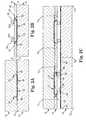
- FIG. 1illustrates single integrated wafer-level package 10 in accordance with the present invention.
- Wafer package 10includes MEMS wafer 12 , microcap 14 , and active device wafer 16 .
- MEMS wafer 12is a film bulk acoustic resonator (FBAR) substrate wafer and active device wafer 16 is a complementary metal oxide semiconductor (CMOS) substrate wafer.
- FBARfilm bulk acoustic resonator
- CMOScomplementary metal oxide semiconductor
- Wafer package 10combines MEMS wafer 12 and active device wafer 16 while each are still at the wafer level into a single integrated wafer package.
- Wafer package 10then includes external contacts ( 40 and 46 discussed further below), which are accessible externally to wafer package 10 , such that it may be electrically coupled to other external components.
- MEMS wafer 12includes MEMS components such as first FBAR 20 and second FBAR 22 on first surface 11 .
- First and second MEMS-wafer contacts 24 and 26are also on first surface 11 of MEMS wafer 12 , and are electrically coupled to first and second FBARs 20 and 22 , respectively.
- first surface 11 of MEMS wafer 12includes peripheral bond pad 28 , which extends around the periphery of first surface 11 of MEMS wafer 12 .
- Microcap 14includes first and second surfaces 13 and 15 .
- First microcap via 32 and second microcap via 34extend though microcap 14 from first surface 13 to second surface 15 .
- First microcap contact 32 Aextends within first via 32 and along second surface 15 .
- second microcap contact 34 Aextends within second via 34 and along second surface 15 .
- Active device wafer 16includes first surface 17 , which carries active device circuitry, such a CMOS circuit.
- First and second active-wafer inside bond pads 42 and 44are adjacent first surface 17
- first and second active-wafer outside bond pads 40 and 46are adjacent first surface 17 .
- Bond pads 42 through 46provide electrical connectivity to the active device circuitry of active device wafer 16 .
- First and second active-wafer columns 36 and 38are between first surface 17 of active device wafer 16 and second surface 15 of microcap 14 .
- microcap 14protects MEMS wafer 12 , and also provides electrical connection with active device wafer 16 .
- wafer package 10is fabricated at a wafer level such that MEMS wafer 12 and active device wafer 16 are already electrically coupled when wafer package 10 is singulated. In this way, the steps of electrically coupling MEMS wafer 12 to an active device wafer 16 after singulation is thereby avoided.
- Microcap 14provides protection and a seal to first and second FBARs 20 and 22 of MEMS wafer 12 .
- the seal providedis a hermetic seal.
- seal ring 30extends between MEMS wafer 12 and microcap 14 around their periphery immediately adjacent bond pad 28 of MEMS wafer 12 . In this way, seal ring 30 surrounds first and second FBARs 20 and 22 .
- the combination of seal ring 30 , first surface 11 of MEMS wafer 12 , and first surface 13 of microcap 14form a hermetic chamber, which hermetically seals first and second FBARs 20 and 22 .
- Seal ring 30may be formed in a variety of ways known in the art in conjunction with microcap 14 .
- Microcap 14may have a similar bond pad or gasket to that of bond pad 28 of MEMS wafer 12 , in order to help seal against seal ring 30 .
- MEMS wafer 12includes electrically conducting first and second contacts 24 and 26 .
- First contact 24is electrically coupled to first FBAR 20 and second contact 26 is electrically coupled to second FBAR 22 .
- Through holes or vias 32 and 34are respectively provided with contacts 32 A and 34 A, which electrically couple to first and seconds 24 and 26 , respectively.
- Vias 32 and 34 , and corresponding contacts 32 A and 34 Aprovide electrical connection with first and second FBARs 20 and 22 through microcap 14 .
- Columns 36 and 38are then electrically connected with contacts 32 A and 34 A, respectively.
- Columns 36 and 38are also coupled electrically to active device wafer 16 .
- first and second inside bond pads 42 and 44are coupled to columns 36 and 38 , respectively.
- microcap 14provides electrical connection between MEMS wafer 12 and active device wafer 16 , while also sealing and protecting first and second FBARs 20 and 22 .
- First and second outside bond pads 40 and 46are provided on active device wafer 16 to provide electrical connection of active device wafer 16 to external devices.
- Wafer package 10may be fabricated in a variety of ways consistent with the present invention. Fabrication of wafer package 10 according to one exemplary fabrication sequence is illustrated in FIGS. 2A-2C .
- MEMS wafer 12is illustrated coupled to microcap 14 .
- microcap 14is illustrated prior to its thinning.
- First and second vias 32 and 34are etched into surface 13 of microcap 14 , which is facing first surface 11 of MEMS wafer 12 .
- First and second vias 32 and 34are aligned with the bond pads on first surface 11 of MEMS wafer 12 . Because microcap 14 has not yet been thinned, vias 32 and 34 are slots into surface 13 and do not penetrate through microcap 14 at this stage.
- FIG. 2Billustrates a later stage of the fabrication sequence where microcap 14 has been thinned downed thereby exposing first and second vias 32 and 34 through second surface 15 of microcap 14 .
- Second surface 15is defined after microcap 14 is thinned to its final dimensions.
- Electrical contacts 32 A and 34 Aare then formed within the exposed vias 32 and 34 .
- First and second columns 36 and 38are then formed over contacts 32 A and 34 A, respectively.
- First and second columns 36 and 38may be formed via any of a variety of bump technologies.
- columns 36 and 38could be flip-chip soldered bumps or copper pillar studs.
- columns 36 and 38are formed as a bump using a solder ball.
- a half sphere of solderis plated, attached to microcap 14 (or to contacts 32 A and 34 A thereon), and then the sphere of solder is melted to make a connection (between contacts 32 A and 34 A of microcap 14 and inside bond pads 42 and 44 of active device wafer 16 ).
- columns 36 and 38are formed as studs. In this case, copper is first plated up to a certain height. This provides a certain stand off distance from microcap 14 to active device wafer 16 .
- FIG. 2Cillustrates a further stage of the fabrication sequence for wafer package 10 .
- the deviceis illustrated oriented 180° rotated from those illustrated in FIGS. 2A and 213 .
- FIG. 2Cillustrates how wafer package 10 is fabricated at the wafer level.
- Multiple wafer packages (also referred to as “die” or “dice”) 10can be cut from the longer wafers illustrated in FIG. 2C .
- cut lines C 1 -C 7indicate the locations of partial saw cuts required to remove a single wafer package 10 .
- Cut lines C 1 , C 2 , C 3 , and C 4are used to release a single wafer package 10 .
- cut lines C 1 and C 2are offset with respect to cut lines C 3 and C 4 .
- these offset cut linesare used so that a standoff distance is provided by the partial saw cuts.
- microcap 14 and MEMS wafer 12are narrower than is active device wafer 16 .
- the standoff distance between microcap 14 /MEMS wafer 12 and active device wafer 16makes outside bond pads 40 and 46 accessible for connecting wafer package 10 with external electronic devices.
- Such connection to outside bond pads 40 and 46could be made, for example, by wire bonding to outside bond pads 40 and 46 .
- first and second columns 36 and 38were illustrated as formed on second surface 15 of microcap 14 after it was thinned.
- first and second columns 36 and 38could have been formed on first surface 17 of active device wafer 16 , which faces microcap 14 when the two are joined.
- MEMS wafer 12may be thinned after attachment to active device wafer 16 , either before or after sawing occurs along the various cut lines.
- Wafer package 10is illustrated in FIGS. 1 and 2 as including a MEMS wafer 12 that is a FBAR. Specifically, first and second FBARs 20 and 22 are illustrated.
- MEMS wafer 12that is a FBAR.
- first and second FBARs 20 and 22are illustrated.
- MEMS devicesmay be used consistently with the present invention.
- a single FBAR or other MEMS devicesuch as a surface mounted acoustic resonator (SMR) could be used, or a plurality of other MEMS devices can also be used in accordance with the present invention.
- the microcap 14provides both a means for sealing the MEMS devices while at the same time electrically coupling these devices to an active device, such as a CMOS wafer.
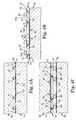
- FIG. 3illustrates single integrated wafer-level package 50 in accordance with an alternative embodiment of the present invention.
- Wafer package 50includes MEMS wafer 52 , microcap 54 , and active device wafer 56 .
- MEMS wafer 52is an FBAR substrate wafer and active device wafer 56 is a CMOS substrate wafer.
- Wafer package 50combines MEMS wafer 52 and active device wafer 56 while each are still at the wafer level into a single integrated wafer package.
- Wafer package 50then includes external contacts ( 88 and 89 discussed further below), which are accessible externally to wafer package 50 , such that it may be electrically coupled to other external components.
- MEMS wafer 52includes MEMS components such as first FBAR 60 and second FBAR 62 on first surface 51 .
- MEMS componentssuch as first FBAR 60 and second FBAR 62 on first surface 51 .
- First and second MEMS-wafer contacts 64 and 66are also on first surface 51 , and are electrically coupled to first and second FBARs 60 and 62 , respectively.
- First surface 51 of MEMS wafer 52also includes MEMS-wafer inner bond pad 68 , which extends around the periphery of first and second FBARs 60 and 62 , and MEMS-wafer outer bond pad 69 , which extends around the periphery of first surface 51 .
- first surface 51 of MEMS wafer 52includes first and second MEMS-wafer vias 90 and 92 , which extend from first surface 51 to second surface 53 .
- MEMS-wafer electrical contacts 90 A and 92 Aare formed within the first and second vias 90 and 92 , respectively, and extend along second surface 53 .
- First and second MEMS-wafer outer columns 88 and 89are electrically coupled to first and second contacts 90 A and 92 B, respectively.
- Microcap 54includes first and second surfaces 55 and 57 .
- First, second, third, and fourth microcap vias 74 , 76 , 78 , and 79extend though microcap 54 from first surface 55 to second surface 57 .
- First, second, third, and fourth microcap electrical contacts 74 A, 76 A, 78 A, and 79 Aare formed within the respective contact vias 74 , 76 , 78 , and 79 , and then each extend along second surface 57 .
- MEMS wafer 52 and microcap 54are aligned and joined such that microcap 54 provides protection and a seal to first and second FBARs 60 and 62 of MEMS wafer 52 .
- the provided sealis hermetic.
- an inner seal ring 70extends between MEMS wafer 52 and microcap 54 around first and second FBARs 60 and 62 immediately adjacent inner bond pad 68 of MEMS wafer 52 .
- inner seal ring 70surrounds first and second FBARs 60 and 62 .
- the combination of inner seal ring 70 , first surface 51 of MEMS wafer 52 , and first surface 55 of microcap 54form a chamber, which hermetically seals first and second FBARs 60 and 62 .
- outer seal ring 71extends between MEMS wafer 52 and microcap 54 around their periphery immediately adjacent outer bond pad 69 of MEMS wafer 52 , providing an additional seal
- Inner and outer seal rings 70 and 71may be formed in a variety of ways known in the art in conjunction with microcaps. In alternative embodiments, outer seal ring 71 may not extend around the periphery of MEMS wafer 52 and microcap 54 , and rather, would help bond MEMS wafer 52 and microcap 54 .
- first contact 74 A of microcap 54is electrically coupled to first contact 90 A of MEMS wafer 52
- fourth contact 79 A of microcap 54is electrically coupled to second contact 92 A of MEMS wafer 52
- a gasket or sealmay also be provided around each of vias 74 , 76 , 78 and 79 where through contacts couple to MEMS wafer 52 .
- Active device wafer 56includes first surface 59 , which carries active device circuitry, such a CMOS circuit.
- First and second active-wafer outer bond pads 94 and 99 , and first and second active-wafer inner bond pads 96 and 98are adjacent first surface 59 of active device wafer 56 .
- Bond pads 94 through 99provide electrical connectivity to the active device circuitry of active device wafer 56 .
- First and second active-wafer outer columns 80 and 86 and first and second active-wafer inner columns 82 and 84are formed between first surface 59 of active device wafer 56 and second surface 57 of microcap 54 , and they align with inner and outer bond pads 94 through 99 .
- microcap 54protects MEMS wafer 52 providing a seal, and also provides electrical connection with active device wafer 56 .
- wafer package 50is fabricated at a wafer level such that MEMS wafer 52 and active device wafer 56 are already electrically coupled when wafer package 50 is singulated. In this way, the steps of electrically coupling MEMS wafer 52 to an active device wafer 56 after singulation is thereby avoided.
- wafer package 50is provided with external electrical contacts such that wafer package 50 is ready for attachment to a circuit.
- Such attachment to other devicesmay be accomplished in a variety of ways consistent with the present invention.
- Wire bondingmay be used to make electrical contact to the package, and in such case studs or bumps on the outer bond pads would not be necessary.
- columns 88 and 89could be coupled directly to a circuit board or other application.
- Other bump bonding, stud bonding, and other types of bondmay electrically connect wafer package 50 to external elements.
- Wafer package 50may be fabricated in a variety of ways consistent with the present invention. Fabrication of wafer package 50 according to one exemplary fabrication sequence is illustrated in FIGS. 4A-4C .
- FIG. 4Aillustrates MEMS wafer 52 adjacent microcap 54 .
- microcap 54has not yet been thinned.
- First; second, third, and fourth vias 74 , 76 , 78 , and 79are illustrated etched into first surface 55 of microcap 54 , which is adjacent first surface 51 of MEMS wafer 52 . Vias 74 through 79 are aligned relative to MEMS wafer 52 such that eventual electrical contacts may, be made through them to MEMS wafer 52 . Because microcap 54 has not yet been thinned, vias 74 , 76 , 78 , and 79 are slots into surface 55 and do not penetrate through microcap 54 at this stage.
- a backside viamay be used.
- thinningmay or may not be utilized, because the via is made from the topside. If thinning is used, it may be done before or after the via is etched.
- FIG. 4Billustrates a subsequent stage of the fabrication sequence for fabricating wafer package 50 according to one embodiment.
- microcap 54has been thinned exposing first through fourth microcap vias 74 through 79 such that they are open on the second surface 57 of microcap 54 , which is facing away from MEMS wafer 52 .
- First, second, third, and fourth electrical contacts 74 A, 76 A, 78 A, and 79 Aare formed in exposed vias 74 , 76 , 78 , and 79 , respectively.
- first and second outer columns 80 and 86are formed on contacts 74 A and 79 A, respectively, and first and second inner columns 82 and 84 are formed on contacts 76 A and 78 A, respectively. In this way, electrical contact is made from MEMS wafer 52 through microcap 54 to inner and outer columns 80 through 86 .
- FIG. 4Cillustrates a further step in the fabrication sequence for wafer package 50 according to one embodiment.
- MEMS wafer 52 and microcap 54 as illustrated in FIG. 4Bare rotated 180° and placed adjacent active device wafer 56 in FIG. 4C .
- active device wafer 56may be rotated.
- first and second outer columns 80 and 86are aligned with first and second outer bond pads 94 and 99 , respectively, and first and second inner columns 82 and 84 are aligned with first and second inner bond pads 96 and 98 , respectively.
- electrical connectionis made between active device wafer 56 through microcap 54 to MEMS wafer 52 , all at the wafer level.
- MEMS wafer 52is then thinned, and first and second MEMS-wafer vias 90 and 92 (illustrated in FIG. 3 ) are added to MEMS wafer 52 , through its second surface 53 .
- contact 90 A and 92 Aare added in first and second vias 90 and 92 , respectively.
- first and second outer columns 88 and 89are fabricated on contacts 90 A and 92 A, respectively.
- wafer package 50provides external electrical connections, via first and second outer columns 88 and 89 , to active device wafer 56 .
- Electrical connection to active device wafer 56is provided at first outer column 88 , to contact 90 A, to contact 74 A, to first outer column 80 , and to first outer bond pad 94 of active device wafer 56 .
- electrical connection to active device wafer 56is provided at second outer column 89 , to contact 92 A, to contact 79 A, to second outer column 86 , and to second outer bond pad 99 of active device wafer 56 .
- these connectionsare illustrative and that some embodiments will include more than two connections.
- a first contact pathis provided via first inner contact 96 on active device wafer 56 , to first inner column 82 , to contact 76 A, to contact 64 , which is in turn coupled to first FBAR 60 .
- a second contact pathis provided via second inner bond pad 98 of active device wafer 56 , to second inner column 84 , to contact 78 A, to contact 66 , which is coupled to second FBAR 62 .
- at least two connectionsare needed for a FBAR, which is not specifically illustrated in the figures.
- the FBARsmay connect to one another to provide one of the connections, or additional connections may be provided similar to those that are illustrated. Electrical connections from external contacts to the active device circuitry and between active device circuitry and the MEMS components are all provided at the wafer level when wafer package 50 is assembled as a single component.
- wafer package 50requires no partial saw with a standoff to allow access to the active device. Instead, outer columns 88 and 89 are provided for electrical connection to other external devices. Alternatively, outer columns 88 and 89 may be avoided and external connection may be made directly to contacts 90 A and 92 A. Inner and outer columns 80 , 82 , 84 , and 86 are described above as active-wafer columns illustrated in FIG. 4B formed on microcap 54 before it is placed on active device wafer 56 . Alternatively, columns 80 through 86 could be formed on active device wafer 56 , and then microcap 54 can be coupled to active device 56 .
- columns 80 through 86may be formed via any of a variety of bump technologies.
- columns 80 though 89could be flip-chip soldered bumps or copper pillar studs.
- columns 80 though 89are formed as a bump using a solder ball. In this case, a half sphere of solder is first plated and attached, and then the sphere of solder is melted to make a connection.
- columns 80 though 89are formed as studs. In this case, copper is first plated up to a certain height. This provides a certain stand off distance from the surface.
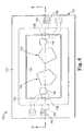
- FIGS. 5 and 6illustrate single integrated wafer-level package 100 in accordance with an alternative embodiment of the present invention.
- FIG. 6illustrates wafer package 100 in a plan view
- FIG. 5illustrates a cross-sectional view taken along line 5 - 5 in FIG. 6 .
- Wafer package 100includes MEMS wafer 102 and active device wafer 104 .
- Active device wafer 104has been removed in FIG. 6 so that those objects below active device wafer 104 may be viewed.
- MEMS wafer 102has first and second surfaces 101 and 103 .
- MEMS wafer 102includes MEMS components, such as first and second FBARs 110 and 112 , on first surface 101 .
- MEMS wafer 102also includes first and second MEMS-wafer outer bond pads 114 and 122 , first and second MEMS-wafer inner bond pads 118 and 120 and MEMS-wafer ring bond pad 116 , all on first surface 101 of MEMS wafer 102 .
- Ring bond pad 116surrounds first and second FBARs 110 and 112 , as illustrated in FIG. 6 .
- MEMS wafer 102also includes first and second MEMS-wafer vias 130 and 132 , which extend between first surface 101 and second surface 103 of MEMS wafer 102 .
- First and second MEMS-wafer contacts 130 A and 132 Aare formed within first and second vias 130 and 132 , respectively, and extend along second surface 103 .
- First and second MEMS-wafer inner bond pads 135 and 137are also provided on the second surface 103 of MEMS wafer 102 .
- first and second MEMS-wafer outer columns 134 and 139are provided on the second surface 103 of MEMS wafer 102 , adjacent contacts 130 A and 132 A, and first and second inner MEMS-wafer columns 136 and 138 are provided on the second surface 103 of MEMS wafer 102 , adjacent first and second inner bond pads 135 and 137 .
- Active device wafer 104includes a first surface 105 , which carries active device circuitry, such as a CMOS circuit.
- First and second active-wafer outer bond pads 150 and 158 , first and second active-wafer inner bond pads 154 and 156 and active-wafer ring bond pad 152are all provided on first surface 105 of active device wafer 104 , and each may provide electrical connectivity to the active device circuitry in active device wafer 104 .
- First and second active-wafer outer columns 140 and 148 , first and second active-wafer inner columns 144 and 148 , and active-wafer ring column 142are provided between first surface 105 of active device wafer 104 and first surface 101 of MEMS wafer 102 .
- ring column 142surrounds first and second FBARs 110 and 112 , as illustrated in FIG. 6 , and is formed adjacent ring bond pad 152 active device wafer 104 and ring bond pad 116 of MEMS wafer 102 .
- First and second outer columns 140 and 148are formed adjacent outer pads 150 and 158 of active device wafer 104 and outer pads 114 and 122 of MEMS wafer 102 .
- First and second inner columns 144 and 146are formed adjacent inner pads 154 and 156 of active device wafer 104 and inner pads 118 and 120 of MEMS wafer 102 .
- the number of bond connectionswill differ with each application, and those illustrated are simply meant to be exemplary and not in any way limiting.
- Inner and outer columns 144 and 146 and 140 and 148provide electrical coupling between active device wafer 104 and MEMS wafer 102 (between bond pads 150 , 154 , 156 and 158 of active device wafer 104 and bond pads 114 , 118 , 120 , and 122 of MEMS wafer 102 ).
- Ring column 142is a ring-like structure that provides a seal around first and second FBARs 110 and 112 . In some embodiments, ring column 142 may also provide a hermetic seal around first and second FBARs 110 and 112 . In some embodiments, ring column 142 can also provide electrical coupling between active device wafer 104 and MEMS wafer 102 (between bond pad 152 of active device wafer 104 and bond pad 116 of MEMS wafer 102 ).
- Whether the seal provided by ring column 142 is hermetictypically depends upon the MEMS device. Where the MEMS device is passivated, the seal provided by ring column 142 may not need to be hermetic. In an application where the MEMS device is an FBAR that is not passivated, seal provided by ring column 142 would need to be hermetic.
- Inner and outer MEMS-wafer columns 136 and 138 and 134 and 139provide external contacts for wafer package 100 . Such external contacts provide a means of connection to other external devices, such as a circuit board.
- First and second MEMS-wafer outer columns 134 and 139provide external connection to active device wafer 104 , and the active device circuit carried thereon. Specifically, first outer column 134 is coupled to contact 130 A, to first outer column 140 , to first outer bond pad 150 of active device wafer 104 . Thus, first outer column 134 provides electrical connectivity to active device circuitry on active device wafer 104 .
- second outer column 139is coupled to contact 132 A, to second outer column 148 , to second outer bond pad 158 of active device wafer 104 .
- these connectionsare illustrative and that some embodiments will include more or less than four connections.
- First and second MEMS-wafer inner columns 136 and 138provide additional external connections to active device wafer 104 .
- any one or combinations of columns 134 , 136 , 138 , and 139may be avoided and external connection may be made directly to one or combinations of contacts 130 A, 135 , 137 , and 132 A.
- traces and additional postsare illustrated as providing additional external electrical connections through to active device wafer 104 , and the active device circuitry thereon.
- Wafer package 100provides a seal for the MEMS components carried on MEMS wafer 102 , which are illustrated as first and second FBARs 110 and 112 .
- the sealis provided between MEMS wafer 102 , active device wafer 104 , and ring column 142 such that no additional microcap is needed.
- the seal providedis a hermetic seal.
- wafer package 100provides external connectors (inner and outer columns 136 and 138 and 134 and 139 ) for electrically coupling external devices to the active device circuitry on active device wafer 104 .
- wafer package 100the combination of MEMS wafer 102 , active device wafer 104 , and ring column protects MEMS components FBARs 110 and 112 , and also provides electrical connection with active device wafer 104 .
- wafer package 100is fabricated at a wafer level such that MEMS wafer 102 and active device wafer 104 are already electrically coupled when wafer package 100 is singulated. In this way, the steps of electrically coupling MEMS wafer 102 to an active device wafer 104 after singulation is thereby avoided.
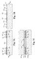
- Wafer package 100may be fabricated in a variety of ways consistent with the present invention. Fabrication of wafer package 100 according to one exemplary fabrication sequence is illustrated in FIGS. 7A through 7C .
- active device wafer 104is illustrated with first and second active-wafer outer bond pads 150 and 158 , first and second active-wafer inner bond pads 154 and 156 and active-wafer ring bond pad 152 are all provided on first surface 105 of active device wafer 104 .
- first and second active-wafer outer columns 140 and 148 , first and second active-wafer inner columns 144 and 146 , and active-wafer ring column 142are provided on the various bond pads 150 through 158 on first surface 105 of active device wafer 104 .
- each of columns 140 through 148may be formed via any of a variety of bump technologies. For example, they could be flip-chip soldered bumps or copper pillar studs.
- columns 140 through 148are formed as a bump using a solder ball. In this case, a half sphere of solder is first attached and plated, and then the sphere of solder is melted to make a connection.
- columns 140 through 148are formed as studs. In this case, copper is first plated up to a certain height. This provides a certain stand off distance from the surface.
- MEMS wafer 102is illustrated with first and second FBARs 110 and 112 , first and second MEMS-wafer outer bond pads 114 and 122 , first and second MEMS-wafer inner bond pads 118 and 120 and MEMS-wafer ring bond pad 116 , all on first surface 101 of MEMS wafer 102 .
- MEMS wafer 102has not yet been thinned, and it has not yet been joined to active device wafer 104 .
- columns 140 through 148may be formed on MEMS wafer 102 as an alternative to forming them on active device wafer 104 .
- MEMS wafer 102is joined with active device wafer 104 , prior to MEMS wafer 102 being thinned.
- Inner and outer columns 144 and 146 and 140 and 148 and ring column 142are all aligned with bond pads 150 through 158 of active device wafer 104 and bond pads 114 through 122 of MEMS wafer 102 in order to provide electrical coupling between active device wafer 104 and MEMS wafer 102 as described above in reference to FIGS. 5 and 6 .
- thinningwould not be needed where a desired thickness is selected initially.
- MEMS wafer 102is thinned and first and second MEMS-wafer vias 130 and 132 are formed.
- MEMS wafer 102may be thinned, and vias 130 and 132 formed, before MEMS wafer 102 and active device wafer 104 are joined.
- First and second contacts 130 A and 132 Aare then formed within first and second vias 130 and 132 , first and second inner bond pads 135 and 137 are added, and inner and outer columns 134 through 139 are added adjacent contacts 130 A and 132 A and inner bond pads 135 and 137 .
- Each of columns 134 through 139may be formed via any of a variety of bump or stud technologies.
- Wafer package 100provides external electrical connection to active device wafer 104 , as well as electrical connection between MEMS wafer 102 and active device wafer 104 .
- a first contact pathis provided via first outer column 134 , which is coupled to contact 130 A, to first outer column 140 , to first outer bond pad 150 of active device wafer 104 .
- a second contact pathis provided via second outer column 139 , which is coupled to contact 132 A, to second outer column 148 , to second outer bond pad 158 of active device wafer 104 . Electrical connections from external contacts to the active device circuitry and between active device circuitry and the MEMS components are all provided at the wafer level when wafer package 100 is assembled as a single component.
- wafer package 100requires no microcap wafer. It also provides external contacts without any partial saw cut with a standoff to allow access to the active device. External contacts inner and outer columns 134 through 139 are provided for electrical connection to other external devices.
Landscapes
- Engineering & Computer Science (AREA)
- Microelectronics & Electronic Packaging (AREA)
- Manufacturing & Machinery (AREA)
- Computer Hardware Design (AREA)
- Physics & Mathematics (AREA)
- Condensed Matter Physics & Semiconductors (AREA)
- General Physics & Mathematics (AREA)
- Power Engineering (AREA)
- Micromachines (AREA)
- Piezo-Electric Or Mechanical Vibrators, Or Delay Or Filter Circuits (AREA)
Abstract
Description
Claims (11)
Priority Applications (1)
| Application Number | Priority Date | Filing Date | Title |
|---|---|---|---|
| US11/686,243US8143082B2 (en) | 2004-12-15 | 2007-03-14 | Wafer bonding of micro-electro mechanical systems to active circuitry |
Applications Claiming Priority (2)
| Application Number | Priority Date | Filing Date | Title |
|---|---|---|---|
| US11/012,589US7202560B2 (en) | 2004-12-15 | 2004-12-15 | Wafer bonding of micro-electro mechanical systems to active circuitry |
| US11/686,243US8143082B2 (en) | 2004-12-15 | 2007-03-14 | Wafer bonding of micro-electro mechanical systems to active circuitry |
Related Parent Applications (1)
| Application Number | Title | Priority Date | Filing Date |
|---|---|---|---|
| US11/012,589DivisionUS7202560B2 (en) | 2004-12-15 | 2004-12-15 | Wafer bonding of micro-electro mechanical systems to active circuitry |
Publications (2)
| Publication Number | Publication Date |
|---|---|
| US20100267182A1 US20100267182A1 (en) | 2010-10-21 |
| US8143082B2true US8143082B2 (en) | 2012-03-27 |
Family
ID=35516316
Family Applications (2)
| Application Number | Title | Priority Date | Filing Date |
|---|---|---|---|
| US11/012,589Expired - LifetimeUS7202560B2 (en) | 2004-12-15 | 2004-12-15 | Wafer bonding of micro-electro mechanical systems to active circuitry |
| US11/686,243Expired - Fee RelatedUS8143082B2 (en) | 2004-12-15 | 2007-03-14 | Wafer bonding of micro-electro mechanical systems to active circuitry |
Family Applications Before (1)
| Application Number | Title | Priority Date | Filing Date |
|---|---|---|---|
| US11/012,589Expired - LifetimeUS7202560B2 (en) | 2004-12-15 | 2004-12-15 | Wafer bonding of micro-electro mechanical systems to active circuitry |
Country Status (4)
| Country | Link |
|---|---|
| US (2) | US7202560B2 (en) |
| JP (1) | JP2006173598A (en) |
| CN (1) | CN1789110B (en) |
| GB (1) | GB2421356B (en) |
Cited By (10)
| Publication number | Priority date | Publication date | Assignee | Title |
|---|---|---|---|---|
| US20100212127A1 (en)* | 2009-02-24 | 2010-08-26 | Habbo Heinze | Process for Adapting Resonance Frequency of a BAW Resonator |
| US20110291261A1 (en)* | 2010-05-27 | 2011-12-01 | International Business Machines Corporation | Three dimensional stacked package structure |
| US20120034724A1 (en)* | 2006-12-05 | 2012-02-09 | Miradia Inc. | Method and apparatus for mems oscillator |
| US20120266673A1 (en)* | 2011-04-22 | 2012-10-25 | Samsung Electro-Mechanics Co., Ltd. | Inertial sensor and method of manufacturing the same |
| US20130020713A1 (en)* | 2009-09-25 | 2013-01-24 | Chirayarikathu Veedu Sankarapillai Premachandran | Wafer Level Package and a Method of Forming a Wafer Level Package |
| US9257834B1 (en) | 2015-02-13 | 2016-02-09 | The Silanna Group Pty Ltd. | Single-laminate galvanic isolator assemblies |
| US9359193B2 (en) | 2013-01-28 | 2016-06-07 | Asia Pacific Microsystems, Inc. | Method for manufacturing an integrated MEMS device |
| US20160301382A1 (en)* | 2013-12-25 | 2016-10-13 | Murata Manufacturing Co., Ltd. | Electronic component module |
| US20170023426A1 (en)* | 2014-04-04 | 2017-01-26 | Ando Lars Feyh | Membrane-Based Sensor and Method for Robust Manufacture of a Membrane-Based Sensor |
| US20230056318A1 (en)* | 2017-10-05 | 2023-02-23 | Google Llc | Low footprint resonator in flip chip geometry |
Families Citing this family (42)
| Publication number | Priority date | Publication date | Assignee | Title |
|---|---|---|---|---|
| US7202560B2 (en)* | 2004-12-15 | 2007-04-10 | Avago Technologies Wireless Ip (Singapore) Pte. Ltd. | Wafer bonding of micro-electro mechanical systems to active circuitry |
| KR100661350B1 (en)* | 2004-12-27 | 2006-12-27 | 삼성전자주식회사 | MEMS device package and manufacturing method thereof |
| US20070007983A1 (en)* | 2005-01-06 | 2007-01-11 | Salmon Peter C | Semiconductor wafer tester |
| US7406761B2 (en)* | 2005-03-21 | 2008-08-05 | Honeywell International Inc. | Method of manufacturing vibrating micromechanical structures |
| US7407826B2 (en)* | 2005-03-21 | 2008-08-05 | Honeywell International Inc. | Vacuum packaged single crystal silicon device |
| US20060211233A1 (en)* | 2005-03-21 | 2006-09-21 | Skyworks Solutions, Inc. | Method for fabricating a wafer level package having through wafer vias for external package connectivity and related structure |
| US7576426B2 (en)* | 2005-04-01 | 2009-08-18 | Skyworks Solutions, Inc. | Wafer level package including a device wafer integrated with a passive component |
| US20070004079A1 (en)* | 2005-06-30 | 2007-01-04 | Geefay Frank S | Method for making contact through via contact to an offset contactor inside a cap for the wafer level packaging of FBAR chips |
| US8217473B2 (en)* | 2005-07-29 | 2012-07-10 | Hewlett-Packard Development Company, L.P. | Micro electro-mechanical system packaging and interconnect |
| US20070023923A1 (en)* | 2005-08-01 | 2007-02-01 | Salmon Peter C | Flip chip interface including a mixed array of heat bumps and signal bumps |
| US20070023889A1 (en)* | 2005-08-01 | 2007-02-01 | Salmon Peter C | Copper substrate with feedthroughs and interconnection circuits |
| US7586747B2 (en)* | 2005-08-01 | 2009-09-08 | Salmon Technologies, Llc. | Scalable subsystem architecture having integrated cooling channels |
| US20070093229A1 (en)* | 2005-10-20 | 2007-04-26 | Takehiko Yamakawa | Complex RF device and method for manufacturing the same |
| US7635606B2 (en)* | 2006-08-02 | 2009-12-22 | Skyworks Solutions, Inc. | Wafer level package with cavities for active devices |
| KR100833508B1 (en)* | 2006-12-07 | 2008-05-29 | 한국전자통신연구원 | MEMs package and its method |
| US20080144863A1 (en)* | 2006-12-15 | 2008-06-19 | Fazzio R Shane | Microcap packaging of micromachined acoustic devices |
| US7875942B2 (en)* | 2007-01-04 | 2011-01-25 | Stmicroelectronics, S.R.L. | Electronic device including MEMS devices and holed substrates, in particular of the LGA or BGA type |
| EP1959568A1 (en)* | 2007-02-19 | 2008-08-20 | Consejo Superior de Investigaciones Cientificas | Thin-film bulk acoustic ware resonator and method for performing heterogeneous integration of the same with complementary-metal-oxide-semiconductor integrated circuit |
| US20080217708A1 (en)* | 2007-03-09 | 2008-09-11 | Skyworks Solutions, Inc. | Integrated passive cap in a system-in-package |
| US20080283944A1 (en)* | 2007-05-18 | 2008-11-20 | Geefay Frank S | PHOTOSTRUCTURABLE GLASS MICROELECTROMECHANICAL (MEMs) DEVICES AND METHODS OF MANUFACTURE |
| US8742557B2 (en)* | 2007-06-19 | 2014-06-03 | Honeywell International Inc. | Die mounting stress isolator |
| US8350382B2 (en) | 2007-09-21 | 2013-01-08 | Infineon Technologies Ag | Semiconductor device including electronic component coupled to a backside of a chip |
| KR20150068495A (en) | 2007-11-30 | 2015-06-19 | 스카이워크스 솔루션즈, 인코포레이티드 | Wafer level packaging using flip chip mounting |
| US8900931B2 (en) | 2007-12-26 | 2014-12-02 | Skyworks Solutions, Inc. | In-situ cavity integrated circuit package |
| US20090194829A1 (en)* | 2008-01-31 | 2009-08-06 | Shine Chung | MEMS Packaging Including Integrated Circuit Dies |
| TWI380456B (en)* | 2008-04-30 | 2012-12-21 | Pixart Imaging Inc | Micro-electro-mechanical device and method for making same |
| US9164404B2 (en) | 2008-09-19 | 2015-10-20 | Intel Corporation | System and process for fabricating semiconductor packages |
| US9165841B2 (en) | 2008-09-19 | 2015-10-20 | Intel Corporation | System and process for fabricating semiconductor packages |
| US10040681B2 (en)* | 2009-08-28 | 2018-08-07 | Miradia Inc. | Method and system for MEMS devices |
| US8836449B2 (en) | 2010-08-27 | 2014-09-16 | Wei Pang | Vertically integrated module in a wafer level package |
| US9212051B1 (en) | 2011-08-04 | 2015-12-15 | Western Digital (Fremont), Llc | Systems and methods for forming MEMS assemblies incorporating getters |
| CN103137567B (en)* | 2011-11-30 | 2016-05-25 | 和舰科技(苏州)有限公司 | A kind of crystal circle structure and layout design method that alleviates wafer cutting stress rupture |
| US9040355B2 (en)* | 2012-07-11 | 2015-05-26 | Freescale Semiconductor, Inc. | Sensor package and method of forming same |
| GB2516079A (en)* | 2013-07-10 | 2015-01-14 | Melexis Technologies Nv | Method for hermetically sealing with reduced stress |
| US9802813B2 (en) | 2014-12-24 | 2017-10-31 | Stmicroelectronics (Malta) Ltd | Wafer level package for a MEMS sensor device and corresponding manufacturing process |
| US10790332B2 (en)* | 2015-12-24 | 2020-09-29 | Intel Corporation | Techniques for integrating three-dimensional islands for radio frequency (RF) circuits |
| CN107140598B (en)* | 2017-03-24 | 2018-12-07 | 苏州敏芯微电子技术股份有限公司 | A kind of MEMS and preparation method thereof |
| WO2019132926A1 (en) | 2017-12-28 | 2019-07-04 | Intel Corporation | A front end system having an acoustic wave resonator (awr) on an interposer substrate |
| CN109470367B (en)* | 2018-11-12 | 2020-06-26 | 中国科学院长春光学精密机械与物理研究所 | A kind of preparation method of broadband uncooled infrared detector based on FBAR |
| CN109861665B (en)* | 2018-12-14 | 2021-06-11 | 天津大学 | Piezoelectric acoustic wave filter |
| CN112039491B (en)* | 2020-03-31 | 2022-08-05 | 中芯集成电路(宁波)有限公司 | Thin film piezoelectric acoustic wave filter and manufacturing method thereof |
| US11975961B2 (en)* | 2020-07-31 | 2024-05-07 | Beijing Voyager Technology Co., Ltd. | MEMS package with shock and vibration protection |
Citations (326)
| Publication number | Priority date | Publication date | Assignee | Title |
|---|---|---|---|---|
| US3174122A (en) | 1960-12-12 | 1965-03-16 | Sonus Corp | Frequency selective amplifier |
| US3189851A (en) | 1962-06-04 | 1965-06-15 | Sonus Corp | Piezoelectric filter |
| US3321648A (en) | 1964-06-04 | 1967-05-23 | Sonus Corp | Piezoelectric filter element |
| US3422371A (en) | 1967-07-24 | 1969-01-14 | Sanders Associates Inc | Thin film piezoelectric oscillator |
| GB1207974A (en) | 1966-11-17 | 1970-10-07 | Clevite Corp | Frequency selective apparatus including a piezoelectric device |
| US3582839A (en) | 1968-06-06 | 1971-06-01 | Clevite Corp | Composite coupled-mode filter |
| US3610969A (en) | 1970-02-06 | 1971-10-05 | Mallory & Co Inc P R | Monolithic piezoelectric resonator for use as filter or transformer |
| US3826931A (en) | 1967-10-26 | 1974-07-30 | Hewlett Packard Co | Dual crystal resonator apparatus |
| US3845402A (en) | 1973-02-15 | 1974-10-29 | Edmac Ass Inc | Sonobuoy receiver system, floating coupler |
| US3943016A (en) | 1970-12-07 | 1976-03-09 | General Electric Company | Gallium-phosphorus simultaneous diffusion process |
| US4084217A (en) | 1977-04-19 | 1978-04-11 | Bbc Brown, Boveri & Company, Limited | Alternating-current fed power supply |
| US4172277A (en) | 1977-02-14 | 1979-10-23 | Compagnie Internationale Pour L'informatique Cii-Honeywell Bull (Societe Anonyme) | Chopping control system for a converter in a DC electrical power supply |
| US4272742A (en) | 1978-09-22 | 1981-06-09 | The Secretary Of State For Defence In Her Britannic Majesty's Government Of The United Kingdom Of Great Britain And Northern Ireland | Acoustic wave devices with temperature stabilization |
| US4281299A (en) | 1979-11-23 | 1981-07-28 | Honeywell Inc. | Signal isolator |
| US4320365A (en) | 1980-11-03 | 1982-03-16 | United Technologies Corporation | Fundamental, longitudinal, thickness mode bulk wave resonator |
| GB2013343B (en) | 1978-01-26 | 1982-05-12 | Page Eng Co Ltd | Apparatus for detecting liquid |
| US4344004A (en) | 1980-09-22 | 1982-08-10 | Design Professionals Financial Corp. | Dual function transducer utilizing displacement currents |
| US4355408A (en) | 1980-02-13 | 1982-10-19 | International Computers Limited | System for extracting timing information from a digital waveform |
| US4456850A (en) | 1982-02-09 | 1984-06-26 | Nippon Electric Co., Ltd. | Piezoelectric composite thin film resonator |
| US4529904A (en) | 1983-03-16 | 1985-07-16 | International Standard Electric Corporation | Piezo-electric terminal station for communications system |
| US4556812A (en) | 1983-10-13 | 1985-12-03 | The United States Of America As Represented By The United States Department Of Energy | Acoustic resonator with Al electrodes on an AlN layer and using a GaAs substrate |
| US4608541A (en) | 1984-08-10 | 1986-08-26 | Analog Devices, Kk | Isolation amplifier |
| US4625138A (en) | 1984-10-24 | 1986-11-25 | The United States Of America As Represented By The Secretary Of The Army | Piezoelectric microwave resonator using lateral excitation |
| US4638536A (en) | 1986-01-17 | 1987-01-27 | The United States Of America As Represented By The Secretary Of The Army | Method of making a resonator having a desired frequency from a quartz crystal resonator plate |
| US4640756A (en) | 1983-10-25 | 1987-02-03 | The United States Of America As Represented By The United States Department Of Energy | Method of making a piezoelectric shear wave resonator |
| US4719383A (en) | 1985-05-20 | 1988-01-12 | The United States Of America As Represented By The United States Department Of Energy | Piezoelectric shear wave resonator and method of making same |
| US4769272A (en) | 1987-03-17 | 1988-09-06 | National Semiconductor Corporation | Ceramic lid hermetic seal package structure |
| US4798990A (en) | 1986-09-11 | 1989-01-17 | Bengt Henoch | Device for transmitting electric energy to computers and data nets |
| US4819215A (en) | 1986-01-31 | 1989-04-04 | Showa Electric Wire & Cable Co., Ltd. | Electric signal transfer element |
| US4836882A (en) | 1988-09-12 | 1989-06-06 | The United States Of America As Represented By The Secretary Of The Army | Method of making an acceleration hardened resonator |
| US4841429A (en) | 1988-03-24 | 1989-06-20 | Hughes Aircraft Company | Capacitive coupled power supplies |
| US4906840A (en) | 1988-01-27 | 1990-03-06 | The Board Of Trustees Of Leland Stanford Jr., University | Integrated scanning tunneling microscope |
| US5048038A (en) | 1990-01-25 | 1991-09-10 | The United States Of America As Represented By The United States Department Of Energy | Ion-implanted planar-buried-heterostructure diode laser |
| US5048036A (en) | 1989-09-18 | 1991-09-10 | Spectra Diode Laboratories, Inc. | Heterostructure laser with lattice mismatch |
| US5066925A (en) | 1990-12-10 | 1991-11-19 | Westinghouse Electric Corp. | Multi push-pull MMIC power amplifier |
| US5075641A (en) | 1990-12-04 | 1991-12-24 | Iowa State University Research Foundation, Inc. | High frequency oscillator comprising cointegrated thin film resonator and active device |
| US5111157A (en) | 1991-05-01 | 1992-05-05 | General Electric Company | Power amplifier for broad band operation at frequencies above one ghz and at decade watt power levels |
| US5118982A (en) | 1989-05-31 | 1992-06-02 | Nec Corporation | Thickness mode vibration piezoelectric transformer |
| US5162691A (en) | 1991-01-22 | 1992-11-10 | The United States Of America As Represented By The Secretary Of The Army | Cantilevered air-gap type thin film piezoelectric resonator |
| US5166646A (en) | 1992-02-07 | 1992-11-24 | Motorola, Inc. | Integrated tunable resonators for use in oscillators and filters |
| US5185589A (en) | 1991-05-17 | 1993-02-09 | Westinghouse Electric Corp. | Microwave film bulk acoustic resonator and manifolded filter bank |
| US5214392A (en) | 1988-11-08 | 1993-05-25 | Murata Mfg. Co., Ltd. | Multilayered ceramic type electromagnetic coupler apparatus |
| US5233259A (en) | 1991-02-19 | 1993-08-03 | Westinghouse Electric Corp. | Lateral field FBAR |
| US5241209A (en) | 1990-07-24 | 1993-08-31 | Fujitsu Limited | Semi-conductor device having circuits on both sides of insulation layer and ultrasonic signal path between the circuits |
| US5241456A (en) | 1990-07-02 | 1993-08-31 | General Electric Company | Compact high density interconnect structure |
| US5262347A (en) | 1991-08-14 | 1993-11-16 | Bell Communications Research, Inc. | Palladium welding of a semiconductor body |
| US5270492A (en) | 1991-08-26 | 1993-12-14 | Rohm Co., Ltd. | Structure of lead terminal of electronic device |
| US5294898A (en) | 1992-01-29 | 1994-03-15 | Motorola, Inc. | Wide bandwidth bandpass filter comprising parallel connected piezoelectric resonators |
| US5361077A (en) | 1992-05-29 | 1994-11-01 | Iowa State University Research Foundation, Inc. | Acoustically coupled antenna utilizing an overmoded configuration |
| US5382930A (en) | 1992-12-21 | 1995-01-17 | Trw Inc. | Monolithic multipole filters made of thin film stacked crystal filters |
| US5384808A (en) | 1992-12-31 | 1995-01-24 | Apple Computer, Inc. | Method and apparatus for transmitting NRZ data signals across an isolation barrier disposed in an interface between adjacent devices on a bus |
| EP0637875A1 (en) | 1993-08-04 | 1995-02-08 | Motorola, Inc. | Acoustical isolator and method therefor |
| US5446306A (en) | 1993-12-13 | 1995-08-29 | Trw Inc. | Thin film voltage-tuned semiconductor bulk acoustic resonator (SBAR) |
| US5448014A (en) | 1993-01-27 | 1995-09-05 | Trw Inc. | Mass simultaneous sealing and electrical connection of electronic devices |
| US5465725A (en) | 1993-06-15 | 1995-11-14 | Hewlett Packard Company | Ultrasonic probe |
| US5475351A (en) | 1993-09-24 | 1995-12-12 | Nippon Steel Corporation | Non-contact rotating coupler |
| US5504388A (en) | 1993-03-12 | 1996-04-02 | Ngk Insulators, Ltd. | Piezoelectric/electrostrictive element having electrode film(s) with specified surface roughness |
| US5548189A (en) | 1992-03-26 | 1996-08-20 | Linear Technology Corp. | Fluorescent-lamp excitation circuit using a piezoelectric acoustic transformer and methods for using same |
| US5587620A (en) | 1993-12-21 | 1996-12-24 | Hewlett-Packard Company | Tunable thin film acoustic resonators and method for making the same |
| US5589858A (en) | 1990-05-22 | 1996-12-31 | Canon Kabushiki Kaisha | Information recording apparatus |
| US5594705A (en) | 1994-02-04 | 1997-01-14 | Dynamotive Canada Corporation | Acoustic transformer with non-piezoelectric core |
| US5603324A (en) | 1994-05-19 | 1997-02-18 | Siemens Aktiengesellschaft | Duplexer including a field-effect transistor for use in an ultrasound imaging system |
| US5633574A (en) | 1994-01-18 | 1997-05-27 | Sage; George E. | Pulse-charge battery charger |
| US5666706A (en) | 1993-06-10 | 1997-09-16 | Matsushita Electric Industrial Co., Ltd. | Method of manufacturing a piezoelectric acoustic wave device |
| US5671242A (en) | 1994-09-02 | 1997-09-23 | Mitsubishi Denki Kabushiki Kaisha | Strained quantum well structure |
| US5692279A (en) | 1995-08-17 | 1997-12-02 | Motorola | Method of making a monolithic thin film resonator lattice filter |
| US5704037A (en) | 1996-03-20 | 1997-12-30 | Chen; Mei Yun | Cursor positioning device for computer system |
| US5705877A (en) | 1995-10-12 | 1998-01-06 | Nec Corporation | Piezoelectric transformer driving circuit |
| US5714917A (en) | 1996-10-02 | 1998-02-03 | Nokia Mobile Phones Limited | Device incorporating a tunable thin film bulk acoustic resonator for performing amplitude and phase modulation |
| US5729008A (en) | 1996-01-25 | 1998-03-17 | Hewlett-Packard Company | Method and device for tracking relative movement by correlating signals from an array of photoelements |
| US5789845A (en) | 1994-11-24 | 1998-08-04 | Mitsubishi Denki Kabushiki Kaisha | Film bulk acoustic wave device |
| US5835142A (en) | 1992-02-04 | 1998-11-10 | Matsushita Electric Industrial Co., Ltd. | Direct contact type image sensor and its production method |
| US5853601A (en) | 1997-04-03 | 1998-12-29 | Northrop Grumman Corporation | Top-via etch technique for forming dielectric membranes |
| US5864261A (en) | 1994-05-23 | 1999-01-26 | Iowa State University Research Foundation | Multiple layer acoustical structures for thin-film resonator based circuits and systems |
| US5866969A (en) | 1996-10-24 | 1999-02-02 | Nec Corporation | Actuating circuit of piezoelectric transformer and actuating method thereof |
| US5872493A (en) | 1997-03-13 | 1999-02-16 | Nokia Mobile Phones, Ltd. | Bulk acoustic wave (BAW) filter having a top portion that includes a protective acoustic mirror |
| US5873154A (en) | 1996-10-17 | 1999-02-23 | Nokia Mobile Phones Limited | Method for fabricating a resonator having an acoustic mirror |
| US5894184A (en) | 1996-08-01 | 1999-04-13 | Nec Corporation | Drive circuit for driving a piezoelectric transformer capable of decreasing heat developed from electronic parts composing an inverter circuit |
| US5894647A (en) | 1997-06-30 | 1999-04-20 | Tfr Technologies, Inc. | Method for fabricating piezoelectric resonators and product |
| US5910756A (en) | 1997-05-21 | 1999-06-08 | Nokia Mobile Phones Limited | Filters and duplexers utilizing thin film stacked crystal filter structures and thin film bulk acoustic wave resonators |
| US5932953A (en) | 1997-06-30 | 1999-08-03 | Iowa State University Research Foundation, Inc. | Method and system for detecting material using piezoelectric resonators |
| US5936150A (en) | 1998-04-13 | 1999-08-10 | Rockwell Science Center, Llc | Thin film resonant chemical sensor with resonant acoustic isolator |
| US5953479A (en) | 1998-05-07 | 1999-09-14 | The United States Of America As Represented By The Secretary Of The Army | Tilted valance-band quantum well double heterostructures for single step active and passive optical waveguide device monolithic integration |
| US5955926A (en) | 1996-10-04 | 1999-09-21 | Sanyo Electric Co., Ltd. | Power amplifier and chip carrier |
| US5962787A (en) | 1995-10-24 | 1999-10-05 | Wacoh Corporation | Acceleration sensor |
| US5969463A (en) | 1996-07-10 | 1999-10-19 | Matsushita Electric Industrial Co., Ltd. | Energy trapping piezoelectric device and producing method thereof |
| US5982297A (en) | 1997-10-08 | 1999-11-09 | The Aerospace Corporation | Ultrasonic data communication system |
| US6001664A (en) | 1996-02-01 | 1999-12-14 | Cielo Communications, Inc. | Method for making closely-spaced VCSEL and photodetector on a substrate |
| US6016052A (en) | 1998-04-03 | 2000-01-18 | Cts Corporation | Pulse frequency modulation drive circuit for piezoelectric transformer |
| US6040962A (en) | 1997-05-14 | 2000-03-21 | Tdk Corporation | Magnetoresistive element with conductive films and magnetic domain films overlapping a central active area |
| US6051907A (en) | 1996-10-10 | 2000-04-18 | Nokia Mobile Phones Limited | Method for performing on-wafer tuning of thin film bulk acoustic wave resonators (FBARS) |
| US6060818A (en) | 1998-06-02 | 2000-05-09 | Hewlett-Packard Company | SBAR structures and method of fabrication of SBAR.FBAR film processing techniques for the manufacturing of SBAR/BAR filters |
| US6087198A (en) | 1998-02-12 | 2000-07-11 | Texas Instruments Incorporated | Low cost packaging for thin-film resonators and thin-film resonator-based filters |
| US6090687A (en) | 1998-07-29 | 2000-07-18 | Agilent Technolgies, Inc. | System and method for bonding and sealing microfabricated wafers to form a single structure having a vacuum chamber therein |
| US6107721A (en) | 1999-07-27 | 2000-08-22 | Tfr Technologies, Inc. | Piezoelectric resonators on a differentially offset reflector |
| US6111341A (en) | 1997-02-26 | 2000-08-29 | Toyo Communication Equipment Co., Ltd. | Piezoelectric vibrator and method for manufacturing the same |
| US6111480A (en) | 1997-07-07 | 2000-08-29 | Murata Manfacturing Co., Ltd. | Piezoelectric resonator and method of adjusting resonant frequency thereof |
| US6118181A (en) | 1998-07-29 | 2000-09-12 | Agilent Technologies, Inc. | System and method for bonding wafers |
| US6124678A (en) | 1998-10-08 | 2000-09-26 | Face International Corp. | Fluorescent lamp excitation circuit having a multi-layer piezoelectric acoustic transformer and methods for using the same |
| US6124756A (en) | 1996-04-08 | 2000-09-26 | Texas Instruments Incorporated | Method and apparatus for galvanically isolating two integrated circuits from each other |
| US6131256A (en) | 1995-06-29 | 2000-10-17 | Motorola, Inc. | Temperature compensated resonator and method |
| US6150703A (en) | 1998-06-29 | 2000-11-21 | Trw Inc. | Lateral mode suppression in semiconductor bulk acoustic resonator (SBAR) devices using tapered electrodes, and electrodes edge damping materials |
| US6187513B1 (en) | 1998-05-29 | 2001-02-13 | Sony Corporation | Process for forming mask pattern and process for producing thin film magnetic head |
| US6198208B1 (en) | 1999-05-20 | 2001-03-06 | Tdk Corporation | Thin film piezoelectric device |
| US6215375B1 (en) | 1999-03-30 | 2001-04-10 | Agilent Technologies, Inc. | Bulk acoustic wave resonator with improved lateral mode suppression |
| US6219032B1 (en) | 1995-12-01 | 2001-04-17 | Immersion Corporation | Method for providing force feedback to a user of an interface device based on interactions of a controlled cursor with graphical elements in a graphical user interface |
| US6219263B1 (en) | 1995-05-19 | 2001-04-17 | Sgs-Thomson Microelectronics S.A. | Electronic power supply device |
| US6229247B1 (en) | 1998-11-09 | 2001-05-08 | Face International Corp. | Multi-layer piezoelectric electrical energy transfer device |
| US6228675B1 (en) | 1999-07-23 | 2001-05-08 | Agilent Technologies, Inc. | Microcap wafer-level package with vias |
| US6252229B1 (en) | 1998-07-10 | 2001-06-26 | Boeing North American, Inc. | Sealed-cavity microstructure and microbolometer and associated fabrication methods |
| US6262600B1 (en) | 2000-02-14 | 2001-07-17 | Analog Devices, Inc. | Isolator for transmitting logic signals across an isolation barrier |
| US6262637B1 (en) | 1999-06-02 | 2001-07-17 | Agilent Technologies, Inc. | Duplexer incorporating thin-film bulk acoustic resonators (FBARs) |
| US6263735B1 (en) | 1997-09-10 | 2001-07-24 | Matsushita Electric Industrial Co., Ltd. | Acceleration sensor |
| US6265246B1 (en) | 1999-07-23 | 2001-07-24 | Agilent Technologies, Inc. | Microcap wafer-level package |
| US6278342B1 (en) | 1998-12-30 | 2001-08-21 | Nokia Mobile Phones, Ltd. | Balanced filter structure utilizing bulk acoustic wave resonators having different areas |
| US6292336B1 (en) | 1999-09-30 | 2001-09-18 | Headway Technologies, Inc. | Giant magnetoresistive (GMR) sensor element with enhanced magnetoresistive (MR) coefficient |
| US6307761B1 (en) | 1998-03-23 | 2001-10-23 | Fidelix Y.K. | Single stage high power-factor converter |
| US6307447B1 (en) | 1999-11-01 | 2001-10-23 | Agere Systems Guardian Corp. | Tuning mechanical resonators for electrical filter |
| US6335548B1 (en) | 1999-03-15 | 2002-01-01 | Gentex Corporation | Semiconductor radiation emitter package |
| US20020000646A1 (en) | 2000-02-02 | 2002-01-03 | Raytheon Company, A Delware Corporation | Vacuum package fabrication of integrated circuit components |
| US6355498B1 (en) | 2000-08-11 | 2002-03-12 | Agere Systems Guartian Corp. | Thin film resonators fabricated on membranes created by front side releasing |
| US20020030424A1 (en) | 1999-12-22 | 2002-03-14 | Toyo Communication Equipment Co., Ltd. | High frequency piezoelectric resonator |
| US6366006B1 (en) | 2000-12-15 | 2002-04-02 | Clark Davis Boyd | Composite piezoelectric transformer |
| US6377137B1 (en) | 2000-09-11 | 2002-04-23 | Agilent Technologies, Inc. | Acoustic resonator filter with reduced electromagnetic influence due to die substrate thickness |
| US6384697B1 (en) | 2000-05-08 | 2002-05-07 | Agilent Technologies, Inc. | Cavity spanning bottom electrode of a substrate-mounted bulk wave acoustic resonator |
| US6396200B2 (en) | 1998-01-16 | 2002-05-28 | Mitsubishi Denki Kabushiki Kaisha | Thin film piezoelectric element |
| US20020063497A1 (en) | 2000-01-18 | 2002-05-30 | Panasik Carl M. | Thin Film Resonator And Method |
| US20020070463A1 (en) | 1994-05-09 | 2002-06-13 | Industrial Technology Research Institute | Composite bump bonding |
| US6407649B1 (en) | 2001-01-05 | 2002-06-18 | Nokia Corporation | Monolithic FBAR duplexer and method of making the same |
| US6414569B1 (en) | 1999-11-01 | 2002-07-02 | Murata Manufacturing Co., Ltd. | Method of adjusting frequency of piezoelectric resonance element by removing material from a thicker electrode or adding, material to a thinner electrode |
| US6420820B1 (en) | 2000-08-31 | 2002-07-16 | Agilent Technologies, Inc. | Acoustic wave resonator and method of operating the same to maintain resonance when subjected to temperature variations |
| US6424237B1 (en) | 2000-12-21 | 2002-07-23 | Agilent Technologies, Inc. | Bulk acoustic resonator perimeter reflection system |
| JP2002217676A (en) | 2001-01-17 | 2002-08-02 | Murata Mfg Co Ltd | Piezoelectric filter |
| US6429511B2 (en) | 1999-07-23 | 2002-08-06 | Agilent Technologies, Inc. | Microcap wafer-level package |
| US6434030B1 (en) | 1998-06-12 | 2002-08-13 | Thomas Licensing Sa | Arrangement having a switched-mode power supply and a microprocessor |
| US6437482B1 (en) | 1999-04-19 | 2002-08-20 | Murata Manufacturing Co., Ltd. | Piezoelectric resonator |
| US6441539B1 (en) | 1999-11-11 | 2002-08-27 | Murata Manufacturing Co., Ltd. | Piezoelectric resonator |
| US6441702B1 (en) | 2001-04-27 | 2002-08-27 | Nokia Mobile Phones Ltd. | Method and system for wafer-level tuning of bulk acoustic wave resonators and filters |
| US20020121945A1 (en) | 2001-03-05 | 2002-09-05 | Ruby Richard C. | Method of mass loading of thin film bulk acoustic resonators (fbar) for creating resonators of different frequencies and apparatus embodying the method |
| US20020121944A1 (en) | 2001-03-05 | 2002-09-05 | Larson John D. | Method of providing differential frequency adjusts in a thin film bulk acoustic resonator (FBAR) filter and apparatus embodying the method |
| US20020126517A1 (en) | 2001-01-24 | 2002-09-12 | Nissin Electric Co., Ltd. | DC-DC converter and bi-directional DC-DC converter and method of controlling the same |
| US20020140520A1 (en) | 2001-03-30 | 2002-10-03 | Hitachi Media Electronics Co., Ltd. | Radio frequency fliter, radio frequency circuit, antenna duplexer and radio terminal |
| US6462631B2 (en) | 2001-02-14 | 2002-10-08 | Agilent Technologies, Inc. | Passband filter having an asymmetrical filter response |
| US6466418B1 (en) | 2000-02-11 | 2002-10-15 | Headway Technologies, Inc. | Bottom spin valves with continuous spacer exchange (or hard) bias |
| US6466105B1 (en) | 1999-07-07 | 2002-10-15 | Koninklijke Philips Electronics N.V. | Bulk acoustic wave filter |
| US6469909B2 (en) | 2001-01-09 | 2002-10-22 | 3M Innovative Properties Company | MEMS package with flexible circuit interconnect |
| US20020152803A1 (en) | 2001-04-23 | 2002-10-24 | Larson John D. | Systems and methods of monitoring thin film deposition |
| US6472954B1 (en) | 2001-04-23 | 2002-10-29 | Agilent Technologies, Inc. | Controlled effective coupling coefficients for film bulk acoustic resonators |
| US6476536B1 (en) | 2001-04-27 | 2002-11-05 | Nokia Corporation | Method of tuning BAW resonators |
| US6479320B1 (en)* | 2000-02-02 | 2002-11-12 | Raytheon Company | Vacuum package fabrication of microelectromechanical system devices with integrated circuit components |
| US6483229B2 (en) | 2001-03-05 | 2002-11-19 | Agilent Technologies, Inc. | Method of providing differential frequency adjusts in a thin film bulk acoustic resonator (FBAR) filter and apparatus embodying the method |
| US6486751B1 (en) | 2000-09-26 | 2002-11-26 | Agere Systems Inc. | Increased bandwidth thin film resonator having a columnar structure |
| US6489688B1 (en) | 2001-05-02 | 2002-12-03 | Zeevo, Inc. | Area efficient bond pad placement |
| US6492883B2 (en) | 2000-11-03 | 2002-12-10 | Paratek Microwave, Inc. | Method of channel frequency allocation for RF and microwave duplexers |
| US6496085B2 (en) | 2001-01-02 | 2002-12-17 | Nokia Mobile Phones Ltd | Solidly mounted multi-resonator bulk acoustic wave filter with a patterned acoustic mirror |
| US20020190814A1 (en) | 2001-05-11 | 2002-12-19 | Tetsuo Yamada | Thin film bulk acoustic resonator and method of producing the same |
| US6498604B1 (en) | 1997-02-12 | 2002-12-24 | Kanitech A/S | Input device for a computer |
| US20030001251A1 (en) | 2001-01-10 | 2003-01-02 | Cheever James L. | Wafer level interconnection |
| US20030006502A1 (en) | 2000-04-10 | 2003-01-09 | Maurice Karpman | Hermetically sealed microstructure package |
| US20030011446A1 (en) | 2000-10-31 | 2003-01-16 | Paul Bradley | Packaging methodology for duplexers using FBARs |
| US20030011285A1 (en) | 2001-06-27 | 2003-01-16 | Ossmann William J. | Ultrasound transducer |
| US6515558B1 (en) | 2000-11-06 | 2003-02-04 | Nokia Mobile Phones Ltd | Thin-film bulk acoustic resonator with enhanced power handling capacity |
| US6518860B2 (en) | 2001-01-05 | 2003-02-11 | Nokia Mobile Phones Ltd | BAW filters having different center frequencies on a single substrate and a method for providing same |
| US6525996B1 (en) | 1998-12-22 | 2003-02-25 | Seiko Epson Corporation | Power feeding apparatus, power receiving apparatus, power transfer system, power transfer method, portable apparatus, and timepiece |
| US6528344B2 (en) | 2000-06-22 | 2003-03-04 | Samsung Electronics Co., Ltd. | Chip scale surface-mountable packaging method for electronic and MEMS devices |
| US6530515B1 (en) | 2000-09-26 | 2003-03-11 | Amkor Technology, Inc. | Micromachine stacked flip chip package fabrication method |
| US6534900B2 (en) | 2000-02-18 | 2003-03-18 | Infineon Technologies Ag | Piezoresonator |
| US20030051550A1 (en) | 2001-08-16 | 2003-03-20 | Nguyen Clark T.-C. | Mechanical resonator device having phenomena-dependent electrical stiffness |
| US6542055B1 (en) | 2000-10-31 | 2003-04-01 | Agilent Technologies, Inc. | Integrated filter balun |
| US6549394B1 (en) | 2002-03-22 | 2003-04-15 | Agilent Technologies, Inc. | Micromachined parallel-plate variable capacitor with plate suspension |
| US6548943B2 (en) | 2001-04-12 | 2003-04-15 | Nokia Mobile Phones Ltd. | Method of producing thin-film bulk acoustic wave devices |
| US6550664B2 (en) | 2000-12-09 | 2003-04-22 | Agilent Technologies, Inc. | Mounting film bulk acoustic resonators in microwave packages using flip chip bonding technology |
| JP2003124779A (en) | 2001-10-16 | 2003-04-25 | Tdk Corp | Piezoelectric vibrator, piezoelectric vibration component and manufacturing method thereof |
| US6559530B2 (en) | 2001-09-19 | 2003-05-06 | Raytheon Company | Method of integrating MEMS device with low-resistivity silicon substrates |
| US6559487B1 (en) | 1999-11-01 | 2003-05-06 | Samsung Electronics Co., Ltd. | High-vacuum packaged microgyroscope and method for manufacturing the same |
| US20030087469A1 (en) | 2001-11-02 | 2003-05-08 | Intel Corporation | Method of fabricating an integrated circuit that seals a MEMS device within a cavity |
| US6564448B1 (en) | 1998-05-08 | 2003-05-20 | Nec Corporation | Resin structure in which manufacturing cost is cheap and sufficient adhesive strength can be obtained and method of manufacturing it |
| US6566956B2 (en) | 2000-07-14 | 2003-05-20 | Hitachi, Ltd. | High frequency power amplifier |
| US20030102776A1 (en) | 2001-11-29 | 2003-06-05 | Matsushita Electric Industrial Co., Ltd. | Driving circuit for piezoelectric transformer, cold-cathode tube light-emitting apparatus, liquid crystal panel and device with built-in liquid crystal panel |
| DE10160617A1 (en) | 2001-12-11 | 2003-06-12 | Epcos Ag | Acoustic mirror with improved reflection |
| US6580159B1 (en) | 1999-11-05 | 2003-06-17 | Amkor Technology, Inc. | Integrated circuit device packages and substrates for making the packages |
| US20030111439A1 (en) | 2001-12-14 | 2003-06-19 | Fetter Linus Albert | Method of forming tapered electrodes for electronic devices |
| US6583688B2 (en) | 2000-04-06 | 2003-06-24 | Koninklijke Philips Electronics N.V. | Tunable filter arrangement comprising resonators with reflection layers |
| US6583374B2 (en) | 2001-02-20 | 2003-06-24 | Rockwell Automation Technologies, Inc. | Microelectromechanical system (MEMS) digital electrical isolator |
| US20030128081A1 (en) | 2002-01-09 | 2003-07-10 | Nokia Corporation | Bulk acoustic wave resonator with two piezoelectric layers as balun in filters and duplexers |
| US6594165B2 (en) | 2001-04-12 | 2003-07-15 | Koninklijke Philips Electronics N.V. | Circuit for converting AC voltage into DC voltage |
| US6593870B2 (en) | 2001-10-18 | 2003-07-15 | Rockwell Automation Technologies, Inc. | MEMS-based electrically isolated analog-to-digital converter |
| US20030132809A1 (en) | 2002-01-17 | 2003-07-17 | Chinnugounder Senthilkumar | Oscillator with tunable capacitor |
| US6600390B2 (en) | 2001-12-13 | 2003-07-29 | Agilent Technologies, Inc. | Differential filters with common mode rejection and broadband rejection |
| US20030141946A1 (en) | 2002-01-31 | 2003-07-31 | Ruby Richard C. | Film bulk acoustic resonator (FBAR) and the method of making the same |
| US6601276B2 (en) | 2001-05-11 | 2003-08-05 | Agere Systems Inc. | Method for self alignment of patterned layers in thin film acoustic devices |
| US6603182B1 (en) | 2002-03-12 | 2003-08-05 | Lucent Technologies Inc. | Packaging micromechanical devices |
| US6617249B2 (en) | 2001-03-05 | 2003-09-09 | Agilent Technologies, Inc. | Method for making thin film bulk acoustic resonators (FBARS) with different frequencies on a single substrate and apparatus embodying the method |
| US6617750B2 (en) | 1999-09-21 | 2003-09-09 | Rockwell Automation Technologies, Inc. | Microelectricalmechanical system (MEMS) electrical isolator with reduced sensitivity to inertial noise |
| US6617751B2 (en) | 2000-12-05 | 2003-09-09 | Samsung Electro-Mechanics Co., Ltd. | Film bulk acoustic resonator and method for fabrication thereof |
| US6621137B1 (en) | 2000-10-12 | 2003-09-16 | Intel Corporation | MEMS device integrated chip package, and method of making same |
| US20030179053A1 (en) | 2001-03-23 | 2003-09-25 | Robert Aigner | Filter device |
| US6630753B2 (en) | 2001-10-29 | 2003-10-07 | International Business Machines Corporation | Low cost redundant AC to DC power supply |
| US6635509B1 (en) | 2002-04-12 | 2003-10-21 | Dalsa Semiconductor Inc. | Wafer-level MEMS packaging |
| US6639872B1 (en) | 1997-12-08 | 2003-10-28 | Claus Rein | Remote energy supply process and system for an electronic information carrier |
| US20030205948A1 (en) | 2002-05-03 | 2003-11-06 | Asia Pacific Microsystems, Inc. | Film bulk acoustic device with integrated tunable and trimmable device |
| US6657363B1 (en) | 1998-05-08 | 2003-12-02 | Infineon Technologies Ag | Thin film piezoelectric resonator |
| US20040017130A1 (en) | 2002-07-24 | 2004-01-29 | Li-Peng Wang | Adjusting the frequency of film bulk acoustic resonators |
| US20040016995A1 (en) | 2002-07-25 | 2004-01-29 | Kuo Shun Meen | MEMS control chip integration |
| US6693500B2 (en) | 2001-06-25 | 2004-02-17 | Samsung Electro-Mechanics Co., Ltd. | Film bulk acoustic resonator with improved lateral mode suppression |
| US6710508B2 (en) | 2001-11-27 | 2004-03-23 | Agilent Technologies, Inc. | Method for adjusting and stabilizing the frequency of an acoustic resonator |
| US6710681B2 (en) | 2001-07-13 | 2004-03-23 | Agilent Technologies, Inc. | Thin film bulk acoustic resonator (FBAR) and inductor on a monolithic substrate and method of fabricating the same |
| US20040056735A1 (en) | 2002-09-25 | 2004-03-25 | Murata Manufacturing Co., Ltd. | Piezoelectric resonator, piezoelectric filter, and communication apparatus |
| US6714102B2 (en) | 2001-03-01 | 2004-03-30 | Agilent Technologies, Inc. | Method of fabricating thin film bulk acoustic resonator (FBAR) and FBAR structure embodying the method |
| US6713314B2 (en) | 2002-08-14 | 2004-03-30 | Intel Corporation | Hermetically packaging a microelectromechanical switch and a film bulk acoustic resonator |
| US6720846B2 (en) | 2001-03-21 | 2004-04-13 | Seiko Epson Corporation | Surface acoustic wave device with KNb03 piezoelectric thin film, frequency filter, oscillator, electronic circuit, and electronic apparatus |
| US6720844B1 (en) | 2001-11-16 | 2004-04-13 | Tfr Technologies, Inc. | Coupled resonator bulk acoustic wave filter |
| US6724266B2 (en) | 2000-01-10 | 2004-04-20 | Eta Sa Fabriques D'ebauches | Device for producing a signal having a substantially temperature-independent frequency |
| WO2004034579A1 (en) | 2002-10-08 | 2004-04-22 | Epcos Ag | Bulk acoustic wave resonator and circuit comprising same |
| US20040092234A1 (en) | 2002-11-12 | 2004-05-13 | Nokia Corporation | Crystal-less oscillator transceiver |
| US6738267B1 (en) | 1999-10-19 | 2004-05-18 | Alcatel | Switched power supply converter with a piezoelectric transformer |
| US20040124952A1 (en) | 2002-12-13 | 2004-07-01 | Epcos Ag | Component operating with bulk acoustic waves, and having coupled resonators |
| US20040150293A1 (en) | 2002-12-05 | 2004-08-05 | Michael Unterberger | Component operating with bulk acoustic waves, and having asymmetric/symmetrical circuitry |
| US20040150296A1 (en) | 2003-01-24 | 2004-08-05 | Lg Electronics Inc. | Material sensing sensor and module using thin film bulk acoustic resonator |
| US6774746B2 (en) | 2000-05-24 | 2004-08-10 | Tdk Corporation | Thin film bulk acoustic resonator filters with a piezoelectric layer of lead scandium tantalum oxide |
| US6777263B1 (en) | 2003-08-21 | 2004-08-17 | Agilent Technologies, Inc. | Film deposition to enhance sealing yield of microcap wafer-level package with vias |
| US20040166603A1 (en) | 2003-02-25 | 2004-08-26 | Carley L. Richard | Micromachined assembly with a multi-layer cap defining a cavity |
| US6788170B1 (en) | 1999-07-19 | 2004-09-07 | Nokia Corporation | Resonator structure having a dampening material and a filter having such a resonator structure |
| US6787048B2 (en) | 2001-03-05 | 2004-09-07 | Agilent Technologies, Inc. | Method for producing thin bulk acoustic resonators (FBARs) with different frequencies on the same substrate by subtracting method and apparatus embodying the method |
| US20040195937A1 (en) | 2003-04-01 | 2004-10-07 | Shogo Matsubara | Film bulk acoustic resonator and film bulk acoustic resonator circuit |
| US6803835B2 (en) | 2001-08-30 | 2004-10-12 | Agilent Technologies, Inc. | Integrated filter balun |
| US20040212458A1 (en) | 2002-05-21 | 2004-10-28 | Samsung Electro-Mechanics Co., Ltd. | Film bulk acoustic resonator (FBAR) device and method for fabricating the same |
| WO2004102688A1 (en) | 2003-05-07 | 2004-11-25 | Centre National De La Recherche Scientifique - Cnrs | Electronic circuit comprising embedded piezoelectric transformer |
| US6828713B2 (en) | 2002-07-30 | 2004-12-07 | Agilent Technologies, Inc | Resonator with seed layer |
| US20040257171A1 (en) | 2003-04-18 | 2004-12-23 | Samsung Electronics Co., Ltd. | Air-gap type FBAR, duplexer using the FBAR, and fabricating methods thereof |
| US20040257172A1 (en) | 2003-04-17 | 2004-12-23 | Edgar Schmidhammer | Duplexer with extended functionality |
| US20040263287A1 (en) | 2003-06-30 | 2004-12-30 | Eyal Ginsburg | Tapered electrode in an acoustic resonator |
| US20050012716A1 (en) | 2001-10-24 | 2005-01-20 | Mikulin Dominic Josef | Sensing apparatus |
| US20050012570A1 (en) | 2003-04-30 | 2005-01-20 | Christian Korden | Component functioning with bulk acoustic waves having coupled resonators |
| US20050023931A1 (en) | 2002-11-28 | 2005-02-03 | Stmicroelectronics S.A. | Support and decoupling structure for an acoustic resonator, acoustic resonator and corresponding integrated circuit |
| US6853534B2 (en) | 2003-06-09 | 2005-02-08 | Agilent Technologies, Inc. | Tunable capacitor |
| US20050030126A1 (en) | 2003-08-04 | 2005-02-10 | Tdk Corporation | Filter device and branching filter using same |
| US20050036604A1 (en) | 1997-04-22 | 2005-02-17 | Silicon Laboratories Inc. | Direct digital access arrangement circuitry and method for connecting DSL circuitry to phone lines |
| US20050057117A1 (en) | 2003-09-17 | 2005-03-17 | Hiroshi Nakatsuka | Piezoelectric resonator, filter, and duplexer |
| US20050057324A1 (en) | 2003-09-12 | 2005-03-17 | Keiji Onishi | Thin film bulk acoustic resonator, method for producing the same, filter, composite electronic component device, and communication device |
| US6873065B2 (en) | 1997-10-23 | 2005-03-29 | Analog Devices, Inc. | Non-optical signal isolator |
| US6873529B2 (en) | 2002-02-26 | 2005-03-29 | Kyocera Corporation | High frequency module |
| US6874211B2 (en) | 2001-03-05 | 2005-04-05 | Agilent Technologies, Inc. | Method for producing thin film bulk acoustic resonators (FBARs) with different frequencies on the same substrate by subtracting method and apparatus embodying the method |
| US6888424B2 (en) | 2001-07-03 | 2005-05-03 | Murata Manufacturing Co., Ltd. | Piezoelectric resonator, filter, and electronic communication device |
| US20050093657A1 (en) | 2003-10-30 | 2005-05-05 | Larson John D.Iii | Film acoustically-coupled transformer with reverse C-axis piezoelectric material |
| US20050093653A1 (en) | 2003-10-30 | 2005-05-05 | Larson John D.Iii | Stacked bulk acoustic resonator band-pass filter with controllable pass bandwidth |
| US20050093654A1 (en) | 2003-10-30 | 2005-05-05 | Larson John D.Iii | Decoupled stacked bulk acoustic resonator band-pass filter with controllable pass bandwidth |
| WO2005043756A1 (en) | 2003-10-30 | 2005-05-12 | Agilent Technologies, Inc. | Temperature-compensated film bulk acoustic resonator (fbar) devices |
| US6900705B2 (en) | 2002-03-15 | 2005-05-31 | Matsushita Electric Industrial Co., Ltd. | Balanced high-frequency device and balance-characteristics improving method and balanced high-frequency circuit using the same |
| US6903452B2 (en)* | 2002-04-03 | 2005-06-07 | Intel Corporation | Packaging microelectromechanical structures |
| US6906451B2 (en) | 2002-01-08 | 2005-06-14 | Murata Manufacturing Co., Ltd. | Piezoelectric resonator, piezoelectric filter, duplexer, communication apparatus, and method for manufacturing piezoelectric resonator |
| US6911708B2 (en) | 2003-02-21 | 2005-06-28 | Lg Electronics Inc. | Duplexer filter having film bulk acoustic resonator and semiconductor package thereof |
| US20050140466A1 (en) | 2003-10-30 | 2005-06-30 | Larson John D.Iii | Decoupled stacked bulk acoustic resonator-based band-pass filter |
| US20050167795A1 (en) | 2002-12-27 | 2005-08-04 | Shinko Electric Industries Co., Ltd. | Electronic devices and its production methods |
| US6927651B2 (en) | 2003-05-12 | 2005-08-09 | Agilent Technologies, Inc. | Acoustic resonator devices having multiple resonant frequencies and methods of making the same |
| US6936928B2 (en) | 2000-03-23 | 2005-08-30 | Infineon Technologies Ag | Semiconductor component and method for its production |
| US6936954B2 (en) | 2001-08-29 | 2005-08-30 | Honeywell International Inc. | Bulk resonator |
| US20050193507A1 (en) | 2004-03-04 | 2005-09-08 | Ludwiczak Damian R. | Vibrating debris remover |
| US6943648B2 (en) | 2003-05-01 | 2005-09-13 | Intel Corporation | Methods for forming a frequency bulk acoustic resonator with uniform frequency utilizing multiple trimming layers and structures formed thereby |
| US20050206271A1 (en) | 2004-03-17 | 2005-09-22 | Takamitsu Higuchi | Potassium niobate deposited body, method for manufacturing the same, piezoelectric thin film resonator, frequency filter, frequency oscillator, electronic circuit, and electronic apparatus |
| US20050206483A1 (en) | 2002-08-03 | 2005-09-22 | Pashby Gary J | Sealed integral mems switch |
| US20050218488A1 (en) | 2004-03-31 | 2005-10-06 | Mie Matsuo | Electronic component having micro-electrical mechanical system |
| US6954121B2 (en) | 2003-06-09 | 2005-10-11 | Agilent Technologies, Inc. | Method for controlling piezoelectric coupling coefficient in film bulk acoustic resonators and apparatus embodying the method |
| US6963257B2 (en) | 2004-03-19 | 2005-11-08 | Nokia Corporation | Coupled BAW resonator based duplexers |
| US6970365B2 (en) | 2001-12-12 | 2005-11-29 | Jpmorgan Chase Bank, N.A. | Controlled frequency power factor correction circuit and method |
| US6975183B2 (en) | 2001-10-08 | 2005-12-13 | Infineon Technologies Ag | BAW resonator having piezoelectric layers oriented in opposed directions |
| US6977563B2 (en) | 2002-09-27 | 2005-12-20 | Tdk Corporation | Thin-film piezoelectric resonator and method for fabricating the same |
| US6989723B2 (en) | 2002-12-11 | 2006-01-24 | Tdk Corporation | Piezoelectric resonant filter and duplexer |
| US6998940B2 (en) | 2003-01-15 | 2006-02-14 | Epcos Inc. | Component operating with bulk acoustic waves and a method for producing the component |
| US7002437B2 (en) | 2002-06-11 | 2006-02-21 | Murata Manufacturing Co., Ltd. | Piezoelectric thin-film resonator, piezoelectric filter, and electronic component including the piezoelectric filter |
| WO2006018788A1 (en) | 2004-08-20 | 2006-02-23 | Philips Intellectual Property & Standards Gmbh | Narrow band bulk acoustic wave filter |
| US7019604B2 (en) | 2002-07-23 | 2006-03-28 | Murata Manufacturing Co., Ltd. | Piezoelectric filter, duplexer, composite piezoelectric resonator, communication device and method for adjusting frequency of piezoelectric filter |
| GB2418791A (en) | 2004-10-01 | 2006-04-05 | Agilent Technologies Inc | Improved Q for FBAR-type acoustic resonators |
| US20060071736A1 (en) | 2004-10-01 | 2006-04-06 | Ruby Richard C | Acoustic resonator performance enhancement using alternating frame structure |
| US7026876B1 (en) | 2003-02-21 | 2006-04-11 | Dynalinear Technologies, Inc. | High linearity smart HBT power amplifiers for CDMA/WCDMA application |
| US20060081048A1 (en) | 2003-08-04 | 2006-04-20 | Atsushi Mikado | Acceleration sensor |
| US20060087199A1 (en) | 2004-10-22 | 2006-04-27 | Larson John D Iii | Piezoelectric isolating transformer |
| EP1528677B1 (en) | 2003-10-30 | 2006-05-10 | Agilent Technologies, Inc. | Film acoustically-coupled transformer with two reverse c-axis piezoelectric elements |
| US20060103492A1 (en) | 2004-11-15 | 2006-05-18 | Hongjun Feng | Thin film bulk acoustic resonator with a mass loaded perimeter |
| US7057476B2 (en) | 2003-12-30 | 2006-06-06 | Industrial Technology Research Institute | Noise suppression method for wave filter |
| US20060119453A1 (en) | 2004-11-12 | 2006-06-08 | Infineon Technologies Ag | Thin-film BAW filter, and a method for production of a thin-film BAW filter |
| US20060125489A1 (en) | 2002-07-19 | 2006-06-15 | Hans-Dieter Feucht | Device and method for detecting a substance |
| US7064606B2 (en) | 2003-03-28 | 2006-06-20 | Andrew Corporation | High efficiency amplifier and method of designing same |
| US20060132262A1 (en) | 2004-12-22 | 2006-06-22 | Fazzio Ronald S | Acoustic resonator performance enhancement using selective metal etch |
| US7098758B2 (en) | 2004-11-03 | 2006-08-29 | Avago Technologies Wireless Ip (Singapore) Pte. Ltd. | Acoustically coupled thin-film resonators having an electrode with a tapered edge |
| US20060197411A1 (en) | 2005-03-04 | 2006-09-07 | Hoen Storrs T | Film-bulk acoustic wave resonator with motion plate |
| EP1528676B1 (en) | 2003-10-30 | 2006-09-13 | Avago Technologies General IP (Singapore) Pte. Ltd | Film acoustically-coupled transformer with reverse c-axis piezoelectric material |
| GB2411239B (en) | 2004-02-17 | 2006-10-11 | Transense Technologies Plc | Interrogation method for passive sensor monitoring system |
| US7138889B2 (en) | 2005-03-22 | 2006-11-21 | Triquint Semiconductor, Inc. | Single-port multi-resonator acoustic resonator device |
| US20060284707A1 (en) | 2005-06-20 | 2006-12-21 | Larson John D Iii | Suspended device and method of making |
| US20060290446A1 (en) | 2005-06-22 | 2006-12-28 | Infineon Technologies Ag | BAW apparatus |
| US7161448B2 (en) | 2004-06-14 | 2007-01-09 | Avago Technologies Wireless Ip (Singapore) Pte. Ltd. | Acoustic resonator performance enhancements using recessed region |
| US7170215B2 (en) | 2003-06-18 | 2007-01-30 | Matsushita Electric Industrial Co., Ltd. | Electronic component and method for manufacturing the same |
| US20070037311A1 (en) | 2005-08-10 | 2007-02-15 | Semiconductor Energy Laboratory Co., Ltd. | Manufacturing method of microelectromechanical system |
| US7187254B2 (en) | 2000-11-29 | 2007-03-06 | Tdk Corporation | Film bulk acoustic resonator filters with a coplanar waveguide |
| US7202560B2 (en)* | 2004-12-15 | 2007-04-10 | Avago Technologies Wireless Ip (Singapore) Pte. Ltd. | Wafer bonding of micro-electro mechanical systems to active circuitry |
| US20070080759A1 (en) | 2005-10-06 | 2007-04-12 | Tiberiu Jamneala | Impedance matching and parasitic capacitor resonance of FBAR resonators and coupled filters |
| US20070086274A1 (en) | 2005-10-18 | 2007-04-19 | Ken Nishimura | Acoustically communicating data signals across an electrical isolation barrier |
| US20070085632A1 (en) | 2005-10-18 | 2007-04-19 | Larson John D Iii | Acoustic galvanic isolator |
| US20070086080A1 (en) | 2005-10-18 | 2007-04-19 | Larson John D Iii | Acoustic galvanic isolator incorporating series-connected decoupled stacked bulk acoustic resonators |
| US20070085631A1 (en) | 2005-10-18 | 2007-04-19 | Larson John D Iii | Acoustic galvanic isolator incorporating film acoustically-coupled transformer |
| US20070085447A1 (en) | 2005-10-18 | 2007-04-19 | Larson John D Iii | Acoustic galvanic isolator incorporating single insulated decoupled stacked bulk acoustic resonator with acoustically-resonant electrical insulator |
| US7209374B2 (en) | 2002-12-27 | 2007-04-24 | Yamaha Corporation | Capacitor-input positive and negative power supply circuit |
| US20070090892A1 (en) | 2005-10-18 | 2007-04-26 | Larson John D Iii | Acoustic galvanic isolator incorporating single decoupled stacked bulk acoustic resonator |
| US7212085B2 (en) | 2004-12-30 | 2007-05-01 | Delta Electronics, Inc. | Filter assembly with unbalanced to balanced conversion and reduced noise |
| US20070171002A1 (en) | 2006-01-23 | 2007-07-26 | Unkrich Mark A | Dual path acoustic data coupling system and method |
| US20070170815A1 (en) | 2006-01-23 | 2007-07-26 | Unkrich Mark A | Acoustic data coupling system and method |
| US20070176710A1 (en) | 2006-01-30 | 2007-08-02 | Tiberiu Jamneala | Impedance transforming bulk acoustic wave baluns |
| US20070205850A1 (en) | 2004-11-15 | 2007-09-06 | Tiberiu Jamneala | Piezoelectric resonator structures and electrical filters having frame elements |
| US7275292B2 (en) | 2003-03-07 | 2007-10-02 | Avago Technologies Wireless Ip (Singapore) Pte. Ltd. | Method for fabricating an acoustical resonator on a substrate |
| US7276994B2 (en) | 2002-05-23 | 2007-10-02 | Murata Manufacturing Co., Ltd. | Piezoelectric thin-film resonator, piezoelectric filter, and electronic component including the piezoelectric filter |
| US7281304B2 (en) | 2003-04-22 | 2007-10-16 | Samsung Electronics Co., Ltd. | Method for fabricating a film bulk acoustic resonator |
| US7294919B2 (en) | 2003-11-26 | 2007-11-13 | Avago Technologies General Ip (Singapore) Pte. Ltd. | Device having a complaint element pressed between substrates |
| US7301258B2 (en) | 2004-02-05 | 2007-11-27 | Seiko Epson Corporation | Piezoelectric resonator element, piezoelectric resonator, and piezoelectric oscillator |
| US20070279153A1 (en) | 2006-05-31 | 2007-12-06 | Ruby Richard C | Piezoelectric resonator structures and electrical filters |
| US7310861B2 (en) | 2001-09-25 | 2007-12-25 | Infineon Technologies Ag | Method of producing a piezoelectric component |
| US20080055020A1 (en) | 2006-08-31 | 2008-03-06 | Infineon Technologies Ag | Acoustic Resonator |
| US7368857B2 (en) | 2004-03-02 | 2008-05-06 | Seiko Epson Corporation | Piezoelectric resonator element, piezoelectric, resonator, and piezoelectric oscillator |
| US7369013B2 (en) | 2005-04-06 | 2008-05-06 | Avago Technologies Wireless Ip Pte Ltd | Acoustic resonator performance enhancement using filled recessed region |
| EP1575165B1 (en) | 2004-03-09 | 2008-05-07 | Infineon Technologies AG | Bulk acoustic wave filter and method for eliminating unwanted side passands |
| US7388318B2 (en) | 2002-06-20 | 2008-06-17 | Ube Industries, Ltd. | Thin film piezoelectric resonator, thin film piezoelectric device, and manufacturing method thereof |
| US7414495B2 (en) | 2005-06-17 | 2008-08-19 | Matsushita Electric Industrial Co., Ltd. | Coupled FBAR filter |
| US7414349B2 (en) | 2002-10-28 | 2008-08-19 | Matsushita Electric Industrial Co., Ltd. | Piezoelectric vibrator, filter using the same and its adjusting method |
| US20080297280A1 (en) | 2007-05-31 | 2008-12-04 | Robert Thalhammer | Integrated Coupled Resonator Filter and Bulk Acoustic Wave Devices |
| US20080297279A1 (en) | 2007-05-31 | 2008-12-04 | Robert Thalhammer | Coupled Resonator Filter with a Filter Section |
| US7545532B2 (en) | 2001-06-07 | 2009-06-09 | Fujifilm Corporation | Image processing apparatus and image processing program storage medium |
Family Cites Families (4)
| Publication number | Priority date | Publication date | Assignee | Title |
|---|---|---|---|---|
| GB0014963D0 (en) | 2000-06-20 | 2000-08-09 | Koninkl Philips Electronics Nv | A bulk acoustic wave device |
| JP2002374144A (en) | 2001-06-15 | 2002-12-26 | Ube Electronics Ltd | Thin film piezoelectric resonator |
| DE10155927A1 (en) | 2001-11-14 | 2003-06-05 | Infineon Technologies Ag | Passivated BAW resonator and BAW filter |
| US6929974B2 (en)* | 2002-10-18 | 2005-08-16 | Motorola, Inc. | Feedthrough design and method for a hermetically sealed microdevice |
- 2004
- 2004-12-15USUS11/012,589patent/US7202560B2/ennot_activeExpired - Lifetime
- 2005
- 2005-11-03GBGB0522505Apatent/GB2421356B/ennot_activeExpired - Fee Related
- 2005-11-10CNCN200510117764XApatent/CN1789110B/ennot_activeExpired - Fee Related
- 2005-11-28JPJP2005341710Apatent/JP2006173598A/enactivePending
- 2007
- 2007-03-14USUS11/686,243patent/US8143082B2/ennot_activeExpired - Fee Related
Patent Citations (400)
| Publication number | Priority date | Publication date | Assignee | Title |
|---|---|---|---|---|
| US3174122A (en) | 1960-12-12 | 1965-03-16 | Sonus Corp | Frequency selective amplifier |
| US3189851A (en) | 1962-06-04 | 1965-06-15 | Sonus Corp | Piezoelectric filter |
| US3321648A (en) | 1964-06-04 | 1967-05-23 | Sonus Corp | Piezoelectric filter element |
| GB1207974A (en) | 1966-11-17 | 1970-10-07 | Clevite Corp | Frequency selective apparatus including a piezoelectric device |
| US3590287A (en) | 1966-11-17 | 1971-06-29 | Clevite Corp | Piezoelectric thin multilayer composite resonators |
| US3422371A (en) | 1967-07-24 | 1969-01-14 | Sanders Associates Inc | Thin film piezoelectric oscillator |
| US3568108A (en) | 1967-07-24 | 1971-03-02 | Sanders Associates Inc | Thin film piezoelectric filter |
| US3826931A (en) | 1967-10-26 | 1974-07-30 | Hewlett Packard Co | Dual crystal resonator apparatus |
| US3582839A (en) | 1968-06-06 | 1971-06-01 | Clevite Corp | Composite coupled-mode filter |
| US3610969A (en) | 1970-02-06 | 1971-10-05 | Mallory & Co Inc P R | Monolithic piezoelectric resonator for use as filter or transformer |
| US3943016A (en) | 1970-12-07 | 1976-03-09 | General Electric Company | Gallium-phosphorus simultaneous diffusion process |
| US3845402A (en) | 1973-02-15 | 1974-10-29 | Edmac Ass Inc | Sonobuoy receiver system, floating coupler |
| US4172277A (en) | 1977-02-14 | 1979-10-23 | Compagnie Internationale Pour L'informatique Cii-Honeywell Bull (Societe Anonyme) | Chopping control system for a converter in a DC electrical power supply |
| US4084217A (en) | 1977-04-19 | 1978-04-11 | Bbc Brown, Boveri & Company, Limited | Alternating-current fed power supply |
| GB2013343B (en) | 1978-01-26 | 1982-05-12 | Page Eng Co Ltd | Apparatus for detecting liquid |
| US4272742A (en) | 1978-09-22 | 1981-06-09 | The Secretary Of State For Defence In Her Britannic Majesty's Government Of The United Kingdom Of Great Britain And Northern Ireland | Acoustic wave devices with temperature stabilization |
| US4281299A (en) | 1979-11-23 | 1981-07-28 | Honeywell Inc. | Signal isolator |
| US4355408A (en) | 1980-02-13 | 1982-10-19 | International Computers Limited | System for extracting timing information from a digital waveform |
| US4344004A (en) | 1980-09-22 | 1982-08-10 | Design Professionals Financial Corp. | Dual function transducer utilizing displacement currents |
| US4320365A (en) | 1980-11-03 | 1982-03-16 | United Technologies Corporation | Fundamental, longitudinal, thickness mode bulk wave resonator |
| US4456850A (en) | 1982-02-09 | 1984-06-26 | Nippon Electric Co., Ltd. | Piezoelectric composite thin film resonator |
| US4529904A (en) | 1983-03-16 | 1985-07-16 | International Standard Electric Corporation | Piezo-electric terminal station for communications system |
| US4556812A (en) | 1983-10-13 | 1985-12-03 | The United States Of America As Represented By The United States Department Of Energy | Acoustic resonator with Al electrodes on an AlN layer and using a GaAs substrate |
| US4640756A (en) | 1983-10-25 | 1987-02-03 | The United States Of America As Represented By The United States Department Of Energy | Method of making a piezoelectric shear wave resonator |
| US4608541A (en) | 1984-08-10 | 1986-08-26 | Analog Devices, Kk | Isolation amplifier |
| US4625138A (en) | 1984-10-24 | 1986-11-25 | The United States Of America As Represented By The Secretary Of The Army | Piezoelectric microwave resonator using lateral excitation |
| US4719383A (en) | 1985-05-20 | 1988-01-12 | The United States Of America As Represented By The United States Department Of Energy | Piezoelectric shear wave resonator and method of making same |
| US4638536A (en) | 1986-01-17 | 1987-01-27 | The United States Of America As Represented By The Secretary Of The Army | Method of making a resonator having a desired frequency from a quartz crystal resonator plate |
| US4819215A (en) | 1986-01-31 | 1989-04-04 | Showa Electric Wire & Cable Co., Ltd. | Electric signal transfer element |
| US4798990A (en) | 1986-09-11 | 1989-01-17 | Bengt Henoch | Device for transmitting electric energy to computers and data nets |
| US4769272A (en) | 1987-03-17 | 1988-09-06 | National Semiconductor Corporation | Ceramic lid hermetic seal package structure |
| US4906840A (en) | 1988-01-27 | 1990-03-06 | The Board Of Trustees Of Leland Stanford Jr., University | Integrated scanning tunneling microscope |
| US5129132A (en) | 1988-01-27 | 1992-07-14 | Board Of Trustees Of The Leland Stanford Jr., University | Method of making an integrated scanning tunneling microscope |
| US4841429A (en) | 1988-03-24 | 1989-06-20 | Hughes Aircraft Company | Capacitive coupled power supplies |
| US4836882A (en) | 1988-09-12 | 1989-06-06 | The United States Of America As Represented By The Secretary Of The Army | Method of making an acceleration hardened resonator |
| US5214392A (en) | 1988-11-08 | 1993-05-25 | Murata Mfg. Co., Ltd. | Multilayered ceramic type electromagnetic coupler apparatus |
| US5118982A (en) | 1989-05-31 | 1992-06-02 | Nec Corporation | Thickness mode vibration piezoelectric transformer |
| US5048036A (en) | 1989-09-18 | 1991-09-10 | Spectra Diode Laboratories, Inc. | Heterostructure laser with lattice mismatch |
| US5048038A (en) | 1990-01-25 | 1991-09-10 | The United States Of America As Represented By The United States Department Of Energy | Ion-implanted planar-buried-heterostructure diode laser |
| US5589858A (en) | 1990-05-22 | 1996-12-31 | Canon Kabushiki Kaisha | Information recording apparatus |
| US5241456A (en) | 1990-07-02 | 1993-08-31 | General Electric Company | Compact high density interconnect structure |
| US5241209A (en) | 1990-07-24 | 1993-08-31 | Fujitsu Limited | Semi-conductor device having circuits on both sides of insulation layer and ultrasonic signal path between the circuits |
| US5075641A (en) | 1990-12-04 | 1991-12-24 | Iowa State University Research Foundation, Inc. | High frequency oscillator comprising cointegrated thin film resonator and active device |
| US5066925A (en) | 1990-12-10 | 1991-11-19 | Westinghouse Electric Corp. | Multi push-pull MMIC power amplifier |
| US5162691A (en) | 1991-01-22 | 1992-11-10 | The United States Of America As Represented By The Secretary Of The Army | Cantilevered air-gap type thin film piezoelectric resonator |
| US5233259A (en) | 1991-02-19 | 1993-08-03 | Westinghouse Electric Corp. | Lateral field FBAR |
| US5111157A (en) | 1991-05-01 | 1992-05-05 | General Electric Company | Power amplifier for broad band operation at frequencies above one ghz and at decade watt power levels |
| US5185589A (en) | 1991-05-17 | 1993-02-09 | Westinghouse Electric Corp. | Microwave film bulk acoustic resonator and manifolded filter bank |
| US5262347A (en) | 1991-08-14 | 1993-11-16 | Bell Communications Research, Inc. | Palladium welding of a semiconductor body |
| US5270492A (en) | 1991-08-26 | 1993-12-14 | Rohm Co., Ltd. | Structure of lead terminal of electronic device |
| US5294898A (en) | 1992-01-29 | 1994-03-15 | Motorola, Inc. | Wide bandwidth bandpass filter comprising parallel connected piezoelectric resonators |
| US5835142A (en) | 1992-02-04 | 1998-11-10 | Matsushita Electric Industrial Co., Ltd. | Direct contact type image sensor and its production method |
| US5166646A (en) | 1992-02-07 | 1992-11-24 | Motorola, Inc. | Integrated tunable resonators for use in oscillators and filters |
| US5548189A (en) | 1992-03-26 | 1996-08-20 | Linear Technology Corp. | Fluorescent-lamp excitation circuit using a piezoelectric acoustic transformer and methods for using same |
| US5361077A (en) | 1992-05-29 | 1994-11-01 | Iowa State University Research Foundation, Inc. | Acoustically coupled antenna utilizing an overmoded configuration |
| US5382930A (en) | 1992-12-21 | 1995-01-17 | Trw Inc. | Monolithic multipole filters made of thin film stacked crystal filters |
| US5384808A (en) | 1992-12-31 | 1995-01-24 | Apple Computer, Inc. | Method and apparatus for transmitting NRZ data signals across an isolation barrier disposed in an interface between adjacent devices on a bus |
| US5448014A (en) | 1993-01-27 | 1995-09-05 | Trw Inc. | Mass simultaneous sealing and electrical connection of electronic devices |
| US5504388A (en) | 1993-03-12 | 1996-04-02 | Ngk Insulators, Ltd. | Piezoelectric/electrostrictive element having electrode film(s) with specified surface roughness |
| US5666706A (en) | 1993-06-10 | 1997-09-16 | Matsushita Electric Industrial Co., Ltd. | Method of manufacturing a piezoelectric acoustic wave device |
| US5465725A (en) | 1993-06-15 | 1995-11-14 | Hewlett Packard Company | Ultrasonic probe |
| EP0637875A1 (en) | 1993-08-04 | 1995-02-08 | Motorola, Inc. | Acoustical isolator and method therefor |
| US5475351A (en) | 1993-09-24 | 1995-12-12 | Nippon Steel Corporation | Non-contact rotating coupler |
| US5446306A (en) | 1993-12-13 | 1995-08-29 | Trw Inc. | Thin film voltage-tuned semiconductor bulk acoustic resonator (SBAR) |
| US5873153A (en) | 1993-12-21 | 1999-02-23 | Hewlett-Packard Company | Method of making tunable thin film acoustic resonators |
| US6507983B1 (en) | 1993-12-21 | 2003-01-21 | Agilent Technologies, Inc. | Method of making tunable thin film acoustic resonators |
| US5587620A (en) | 1993-12-21 | 1996-12-24 | Hewlett-Packard Company | Tunable thin film acoustic resonators and method for making the same |
| US5633574A (en) | 1994-01-18 | 1997-05-27 | Sage; George E. | Pulse-charge battery charger |
| US5594705A (en) | 1994-02-04 | 1997-01-14 | Dynamotive Canada Corporation | Acoustic transformer with non-piezoelectric core |
| US20020070463A1 (en) | 1994-05-09 | 2002-06-13 | Industrial Technology Research Institute | Composite bump bonding |
| US5603324A (en) | 1994-05-19 | 1997-02-18 | Siemens Aktiengesellschaft | Duplexer including a field-effect transistor for use in an ultrasound imaging system |
| US5864261A (en) | 1994-05-23 | 1999-01-26 | Iowa State University Research Foundation | Multiple layer acoustical structures for thin-film resonator based circuits and systems |
| US5671242A (en) | 1994-09-02 | 1997-09-23 | Mitsubishi Denki Kabushiki Kaisha | Strained quantum well structure |
| US5789845A (en) | 1994-11-24 | 1998-08-04 | Mitsubishi Denki Kabushiki Kaisha | Film bulk acoustic wave device |
| US6219263B1 (en) | 1995-05-19 | 2001-04-17 | Sgs-Thomson Microelectronics S.A. | Electronic power supply device |
| US6131256A (en) | 1995-06-29 | 2000-10-17 | Motorola, Inc. | Temperature compensated resonator and method |
| US5692279A (en) | 1995-08-17 | 1997-12-02 | Motorola | Method of making a monolithic thin film resonator lattice filter |
| US5705877A (en) | 1995-10-12 | 1998-01-06 | Nec Corporation | Piezoelectric transformer driving circuit |
| US5962787A (en) | 1995-10-24 | 1999-10-05 | Wacoh Corporation | Acceleration sensor |
| US6219032B1 (en) | 1995-12-01 | 2001-04-17 | Immersion Corporation | Method for providing force feedback to a user of an interface device based on interactions of a controlled cursor with graphical elements in a graphical user interface |
| US5729008A (en) | 1996-01-25 | 1998-03-17 | Hewlett-Packard Company | Method and device for tracking relative movement by correlating signals from an array of photoelements |
| US6001664A (en) | 1996-02-01 | 1999-12-14 | Cielo Communications, Inc. | Method for making closely-spaced VCSEL and photodetector on a substrate |
| US5704037A (en) | 1996-03-20 | 1997-12-30 | Chen; Mei Yun | Cursor positioning device for computer system |
| US6124756A (en) | 1996-04-08 | 2000-09-26 | Texas Instruments Incorporated | Method and apparatus for galvanically isolating two integrated circuits from each other |
| US5969463A (en) | 1996-07-10 | 1999-10-19 | Matsushita Electric Industrial Co., Ltd. | Energy trapping piezoelectric device and producing method thereof |
| US5894184A (en) | 1996-08-01 | 1999-04-13 | Nec Corporation | Drive circuit for driving a piezoelectric transformer capable of decreasing heat developed from electronic parts composing an inverter circuit |
| US5714917A (en) | 1996-10-02 | 1998-02-03 | Nokia Mobile Phones Limited | Device incorporating a tunable thin film bulk acoustic resonator for performing amplitude and phase modulation |
| US5955926A (en) | 1996-10-04 | 1999-09-21 | Sanyo Electric Co., Ltd. | Power amplifier and chip carrier |
| US6051907A (en) | 1996-10-10 | 2000-04-18 | Nokia Mobile Phones Limited | Method for performing on-wafer tuning of thin film bulk acoustic wave resonators (FBARS) |
| US5873154A (en) | 1996-10-17 | 1999-02-23 | Nokia Mobile Phones Limited | Method for fabricating a resonator having an acoustic mirror |
| US5866969A (en) | 1996-10-24 | 1999-02-02 | Nec Corporation | Actuating circuit of piezoelectric transformer and actuating method thereof |
| US6498604B1 (en) | 1997-02-12 | 2002-12-24 | Kanitech A/S | Input device for a computer |
| US6111341A (en) | 1997-02-26 | 2000-08-29 | Toyo Communication Equipment Co., Ltd. | Piezoelectric vibrator and method for manufacturing the same |
| US6548942B1 (en) | 1997-02-28 | 2003-04-15 | Texas Instruments Incorporated | Encapsulated packaging for thin-film resonators and thin-film resonator-based filters having a piezoelectric resonator between two acoustic reflectors |
| US5872493A (en) | 1997-03-13 | 1999-02-16 | Nokia Mobile Phones, Ltd. | Bulk acoustic wave (BAW) filter having a top portion that includes a protective acoustic mirror |
| EP0865157B1 (en) | 1997-03-13 | 2009-04-29 | Avago Technologies Wireless IP (Singapore) Pte. Ltd. | A bulk acoustic wave (BAW) filter |
| US5853601A (en) | 1997-04-03 | 1998-12-29 | Northrop Grumman Corporation | Top-via etch technique for forming dielectric membranes |
| US20050036604A1 (en) | 1997-04-22 | 2005-02-17 | Silicon Laboratories Inc. | Direct digital access arrangement circuitry and method for connecting DSL circuitry to phone lines |
| US6040962A (en) | 1997-05-14 | 2000-03-21 | Tdk Corporation | Magnetoresistive element with conductive films and magnetic domain films overlapping a central active area |
| US5910756A (en) | 1997-05-21 | 1999-06-08 | Nokia Mobile Phones Limited | Filters and duplexers utilizing thin film stacked crystal filter structures and thin film bulk acoustic wave resonators |
| US5932953A (en) | 1997-06-30 | 1999-08-03 | Iowa State University Research Foundation, Inc. | Method and system for detecting material using piezoelectric resonators |
| US5894647A (en) | 1997-06-30 | 1999-04-20 | Tfr Technologies, Inc. | Method for fabricating piezoelectric resonators and product |
| US6111480A (en) | 1997-07-07 | 2000-08-29 | Murata Manfacturing Co., Ltd. | Piezoelectric resonator and method of adjusting resonant frequency thereof |
| US6263735B1 (en) | 1997-09-10 | 2001-07-24 | Matsushita Electric Industrial Co., Ltd. | Acceleration sensor |
| US5982297A (en) | 1997-10-08 | 1999-11-09 | The Aerospace Corporation | Ultrasonic data communication system |
| US6873065B2 (en) | 1997-10-23 | 2005-03-29 | Analog Devices, Inc. | Non-optical signal isolator |
| US6639872B1 (en) | 1997-12-08 | 2003-10-28 | Claus Rein | Remote energy supply process and system for an electronic information carrier |
| EP0973256B1 (en) | 1998-01-16 | 2006-09-27 | Mitsubishi Denki Kabushiki Kaisha | Thin film piezoelectric element |
| US6396200B2 (en) | 1998-01-16 | 2002-05-28 | Mitsubishi Denki Kabushiki Kaisha | Thin film piezoelectric element |
| US6087198A (en) | 1998-02-12 | 2000-07-11 | Texas Instruments Incorporated | Low cost packaging for thin-film resonators and thin-film resonator-based filters |
| US6307761B1 (en) | 1998-03-23 | 2001-10-23 | Fidelix Y.K. | Single stage high power-factor converter |
| US6016052A (en) | 1998-04-03 | 2000-01-18 | Cts Corporation | Pulse frequency modulation drive circuit for piezoelectric transformer |
| US5936150A (en) | 1998-04-13 | 1999-08-10 | Rockwell Science Center, Llc | Thin film resonant chemical sensor with resonant acoustic isolator |
| US5953479A (en) | 1998-05-07 | 1999-09-14 | The United States Of America As Represented By The Secretary Of The Army | Tilted valance-band quantum well double heterostructures for single step active and passive optical waveguide device monolithic integration |
| US6564448B1 (en) | 1998-05-08 | 2003-05-20 | Nec Corporation | Resin structure in which manufacturing cost is cheap and sufficient adhesive strength can be obtained and method of manufacturing it |
| US6657363B1 (en) | 1998-05-08 | 2003-12-02 | Infineon Technologies Ag | Thin film piezoelectric resonator |
| US6187513B1 (en) | 1998-05-29 | 2001-02-13 | Sony Corporation | Process for forming mask pattern and process for producing thin film magnetic head |
| US6060818A (en) | 1998-06-02 | 2000-05-09 | Hewlett-Packard Company | SBAR structures and method of fabrication of SBAR.FBAR film processing techniques for the manufacturing of SBAR/BAR filters |
| US6434030B1 (en) | 1998-06-12 | 2002-08-13 | Thomas Licensing Sa | Arrangement having a switched-mode power supply and a microprocessor |
| US6150703A (en) | 1998-06-29 | 2000-11-21 | Trw Inc. | Lateral mode suppression in semiconductor bulk acoustic resonator (SBAR) devices using tapered electrodes, and electrodes edge damping materials |
| US6252229B1 (en) | 1998-07-10 | 2001-06-26 | Boeing North American, Inc. | Sealed-cavity microstructure and microbolometer and associated fabrication methods |
| US6090687A (en) | 1998-07-29 | 2000-07-18 | Agilent Technolgies, Inc. | System and method for bonding and sealing microfabricated wafers to form a single structure having a vacuum chamber therein |
| US6118181A (en) | 1998-07-29 | 2000-09-12 | Agilent Technologies, Inc. | System and method for bonding wafers |
| US6124678A (en) | 1998-10-08 | 2000-09-26 | Face International Corp. | Fluorescent lamp excitation circuit having a multi-layer piezoelectric acoustic transformer and methods for using the same |
| US6229247B1 (en) | 1998-11-09 | 2001-05-08 | Face International Corp. | Multi-layer piezoelectric electrical energy transfer device |
| US6525996B1 (en) | 1998-12-22 | 2003-02-25 | Seiko Epson Corporation | Power feeding apparatus, power receiving apparatus, power transfer system, power transfer method, portable apparatus, and timepiece |
| US6278342B1 (en) | 1998-12-30 | 2001-08-21 | Nokia Mobile Phones, Ltd. | Balanced filter structure utilizing bulk acoustic wave resonators having different areas |
| US6335548B1 (en) | 1999-03-15 | 2002-01-01 | Gentex Corporation | Semiconductor radiation emitter package |
| US6215375B1 (en) | 1999-03-30 | 2001-04-10 | Agilent Technologies, Inc. | Bulk acoustic wave resonator with improved lateral mode suppression |
| EP1047189B1 (en) | 1999-04-19 | 2011-02-16 | Murata Manufacturing Co., Ltd. | Piezoelectric resonator |
| US6437482B1 (en) | 1999-04-19 | 2002-08-20 | Murata Manufacturing Co., Ltd. | Piezoelectric resonator |
| US6198208B1 (en) | 1999-05-20 | 2001-03-06 | Tdk Corporation | Thin film piezoelectric device |
| US6262637B1 (en) | 1999-06-02 | 2001-07-17 | Agilent Technologies, Inc. | Duplexer incorporating thin-film bulk acoustic resonators (FBARs) |
| US6466105B1 (en) | 1999-07-07 | 2002-10-15 | Koninklijke Philips Electronics N.V. | Bulk acoustic wave filter |
| US6788170B1 (en) | 1999-07-19 | 2004-09-07 | Nokia Corporation | Resonator structure having a dampening material and a filter having such a resonator structure |
| US6812619B1 (en) | 1999-07-19 | 2004-11-02 | Nokia Corporation | Resonator structure and a filter comprising such a resonator structure |
| US6376280B1 (en) | 1999-07-23 | 2002-04-23 | Agilent Technologies, Inc. | Microcap wafer-level package |
| US6228675B1 (en) | 1999-07-23 | 2001-05-08 | Agilent Technologies, Inc. | Microcap wafer-level package with vias |
| US6265246B1 (en) | 1999-07-23 | 2001-07-24 | Agilent Technologies, Inc. | Microcap wafer-level package |
| US6429511B2 (en) | 1999-07-23 | 2002-08-06 | Agilent Technologies, Inc. | Microcap wafer-level package |
| US6107721A (en) | 1999-07-27 | 2000-08-22 | Tfr Technologies, Inc. | Piezoelectric resonators on a differentially offset reflector |
| US6617750B2 (en) | 1999-09-21 | 2003-09-09 | Rockwell Automation Technologies, Inc. | Microelectricalmechanical system (MEMS) electrical isolator with reduced sensitivity to inertial noise |
| US6292336B1 (en) | 1999-09-30 | 2001-09-18 | Headway Technologies, Inc. | Giant magnetoresistive (GMR) sensor element with enhanced magnetoresistive (MR) coefficient |
| US6738267B1 (en) | 1999-10-19 | 2004-05-18 | Alcatel | Switched power supply converter with a piezoelectric transformer |
| US6307447B1 (en) | 1999-11-01 | 2001-10-23 | Agere Systems Guardian Corp. | Tuning mechanical resonators for electrical filter |
| US6559487B1 (en) | 1999-11-01 | 2003-05-06 | Samsung Electronics Co., Ltd. | High-vacuum packaged microgyroscope and method for manufacturing the same |
| EP1096259B1 (en) | 1999-11-01 | 2008-12-03 | Samsung Electronics Co., Ltd. | High-vacuum packaged microgyroscope and method for manufacturing the same |
| US20030132493A1 (en) | 1999-11-01 | 2003-07-17 | Samsung Electronics Co., Ltd. | High-vacuum packaged microgyroscope and method for manufacturing the same |
| US6414569B1 (en) | 1999-11-01 | 2002-07-02 | Murata Manufacturing Co., Ltd. | Method of adjusting frequency of piezoelectric resonance element by removing material from a thicker electrode or adding, material to a thinner electrode |
| US6580159B1 (en) | 1999-11-05 | 2003-06-17 | Amkor Technology, Inc. | Integrated circuit device packages and substrates for making the packages |
| EP1100196B1 (en) | 1999-11-11 | 2007-09-05 | Murata Manufacturing Co., Ltd. | Piezoelectric Resonator |
| US6441539B1 (en) | 1999-11-11 | 2002-08-27 | Murata Manufacturing Co., Ltd. | Piezoelectric resonator |
| US20020030424A1 (en) | 1999-12-22 | 2002-03-14 | Toyo Communication Equipment Co., Ltd. | High frequency piezoelectric resonator |
| US6724266B2 (en) | 2000-01-10 | 2004-04-20 | Eta Sa Fabriques D'ebauches | Device for producing a signal having a substantially temperature-independent frequency |
| US20020063497A1 (en) | 2000-01-18 | 2002-05-30 | Panasik Carl M. | Thin Film Resonator And Method |
| US20020000646A1 (en) | 2000-02-02 | 2002-01-03 | Raytheon Company, A Delware Corporation | Vacuum package fabrication of integrated circuit components |
| US6479320B1 (en)* | 2000-02-02 | 2002-11-12 | Raytheon Company | Vacuum package fabrication of microelectromechanical system devices with integrated circuit components |
| US6466418B1 (en) | 2000-02-11 | 2002-10-15 | Headway Technologies, Inc. | Bottom spin valves with continuous spacer exchange (or hard) bias |
| US6262600B1 (en) | 2000-02-14 | 2001-07-17 | Analog Devices, Inc. | Isolator for transmitting logic signals across an isolation barrier |
| US6534900B2 (en) | 2000-02-18 | 2003-03-18 | Infineon Technologies Ag | Piezoresonator |
| US6936928B2 (en) | 2000-03-23 | 2005-08-30 | Infineon Technologies Ag | Semiconductor component and method for its production |
| US6583688B2 (en) | 2000-04-06 | 2003-06-24 | Koninklijke Philips Electronics N.V. | Tunable filter arrangement comprising resonators with reflection layers |
| US20030006502A1 (en) | 2000-04-10 | 2003-01-09 | Maurice Karpman | Hermetically sealed microstructure package |
| US6384697B1 (en) | 2000-05-08 | 2002-05-07 | Agilent Technologies, Inc. | Cavity spanning bottom electrode of a substrate-mounted bulk wave acoustic resonator |
| US6774746B2 (en) | 2000-05-24 | 2004-08-10 | Tdk Corporation | Thin film bulk acoustic resonator filters with a piezoelectric layer of lead scandium tantalum oxide |
| US6528344B2 (en) | 2000-06-22 | 2003-03-04 | Samsung Electronics Co., Ltd. | Chip scale surface-mountable packaging method for electronic and MEMS devices |
| US6566956B2 (en) | 2000-07-14 | 2003-05-20 | Hitachi, Ltd. | High frequency power amplifier |
| US6355498B1 (en) | 2000-08-11 | 2002-03-12 | Agere Systems Guartian Corp. | Thin film resonators fabricated on membranes created by front side releasing |
| EP1180494B1 (en) | 2000-08-11 | 2007-01-03 | Agere Systems, Inc. | Thin film resonators fabricated on membranes created by front side releasing |
| US6874212B2 (en) | 2000-08-31 | 2005-04-05 | Agilent Technologies, Inc. | Method of making an acoustic wave resonator |
| US6420820B1 (en) | 2000-08-31 | 2002-07-16 | Agilent Technologies, Inc. | Acoustic wave resonator and method of operating the same to maintain resonance when subjected to temperature variations |
| US6377137B1 (en) | 2000-09-11 | 2002-04-23 | Agilent Technologies, Inc. | Acoustic resonator filter with reduced electromagnetic influence due to die substrate thickness |
| US6530515B1 (en) | 2000-09-26 | 2003-03-11 | Amkor Technology, Inc. | Micromachine stacked flip chip package fabrication method |
| US6486751B1 (en) | 2000-09-26 | 2002-11-26 | Agere Systems Inc. | Increased bandwidth thin film resonator having a columnar structure |
| US6621137B1 (en) | 2000-10-12 | 2003-09-16 | Intel Corporation | MEMS device integrated chip package, and method of making same |
| US20030011446A1 (en) | 2000-10-31 | 2003-01-16 | Paul Bradley | Packaging methodology for duplexers using FBARs |
| US6542055B1 (en) | 2000-10-31 | 2003-04-01 | Agilent Technologies, Inc. | Integrated filter balun |
| US6492883B2 (en) | 2000-11-03 | 2002-12-10 | Paratek Microwave, Inc. | Method of channel frequency allocation for RF and microwave duplexers |
| US6515558B1 (en) | 2000-11-06 | 2003-02-04 | Nokia Mobile Phones Ltd | Thin-film bulk acoustic resonator with enhanced power handling capacity |
| US7187254B2 (en) | 2000-11-29 | 2007-03-06 | Tdk Corporation | Film bulk acoustic resonator filters with a coplanar waveguide |
| US6617751B2 (en) | 2000-12-05 | 2003-09-09 | Samsung Electro-Mechanics Co., Ltd. | Film bulk acoustic resonator and method for fabrication thereof |
| US6550664B2 (en) | 2000-12-09 | 2003-04-22 | Agilent Technologies, Inc. | Mounting film bulk acoustic resonators in microwave packages using flip chip bonding technology |
| US6366006B1 (en) | 2000-12-15 | 2002-04-02 | Clark Davis Boyd | Composite piezoelectric transformer |
| US6424237B1 (en) | 2000-12-21 | 2002-07-23 | Agilent Technologies, Inc. | Bulk acoustic resonator perimeter reflection system |
| US6496085B2 (en) | 2001-01-02 | 2002-12-17 | Nokia Mobile Phones Ltd | Solidly mounted multi-resonator bulk acoustic wave filter with a patterned acoustic mirror |
| US6518860B2 (en) | 2001-01-05 | 2003-02-11 | Nokia Mobile Phones Ltd | BAW filters having different center frequencies on a single substrate and a method for providing same |
| US6407649B1 (en) | 2001-01-05 | 2002-06-18 | Nokia Corporation | Monolithic FBAR duplexer and method of making the same |
| US6469909B2 (en) | 2001-01-09 | 2002-10-22 | 3M Innovative Properties Company | MEMS package with flexible circuit interconnect |
| US20030001251A1 (en) | 2001-01-10 | 2003-01-02 | Cheever James L. | Wafer level interconnection |
| JP2002217676A (en) | 2001-01-17 | 2002-08-02 | Murata Mfg Co Ltd | Piezoelectric filter |
| US20020126517A1 (en) | 2001-01-24 | 2002-09-12 | Nissin Electric Co., Ltd. | DC-DC converter and bi-directional DC-DC converter and method of controlling the same |
| US6462631B2 (en) | 2001-02-14 | 2002-10-08 | Agilent Technologies, Inc. | Passband filter having an asymmetrical filter response |
| US6583374B2 (en) | 2001-02-20 | 2003-06-24 | Rockwell Automation Technologies, Inc. | Microelectromechanical system (MEMS) digital electrical isolator |
| US6714102B2 (en) | 2001-03-01 | 2004-03-30 | Agilent Technologies, Inc. | Method of fabricating thin film bulk acoustic resonator (FBAR) and FBAR structure embodying the method |
| US6874211B2 (en) | 2001-03-05 | 2005-04-05 | Agilent Technologies, Inc. | Method for producing thin film bulk acoustic resonators (FBARs) with different frequencies on the same substrate by subtracting method and apparatus embodying the method |
| US6566979B2 (en) | 2001-03-05 | 2003-05-20 | Agilent Technologies, Inc. | Method of providing differential frequency adjusts in a thin film bulk acoustic resonator (FBAR) filter and apparatus embodying the method |
| US6787048B2 (en) | 2001-03-05 | 2004-09-07 | Agilent Technologies, Inc. | Method for producing thin bulk acoustic resonators (FBARs) with different frequencies on the same substrate by subtracting method and apparatus embodying the method |
| US6469597B2 (en) | 2001-03-05 | 2002-10-22 | Agilent Technologies, Inc. | Method of mass loading of thin film bulk acoustic resonators (FBAR) for creating resonators of different frequencies and apparatus embodying the method |
| US20020121945A1 (en) | 2001-03-05 | 2002-09-05 | Ruby Richard C. | Method of mass loading of thin film bulk acoustic resonators (fbar) for creating resonators of different frequencies and apparatus embodying the method |
| US6617249B2 (en) | 2001-03-05 | 2003-09-09 | Agilent Technologies, Inc. | Method for making thin film bulk acoustic resonators (FBARS) with different frequencies on a single substrate and apparatus embodying the method |
| US20020121944A1 (en) | 2001-03-05 | 2002-09-05 | Larson John D. | Method of providing differential frequency adjusts in a thin film bulk acoustic resonator (FBAR) filter and apparatus embodying the method |
| US6483229B2 (en) | 2001-03-05 | 2002-11-19 | Agilent Technologies, Inc. | Method of providing differential frequency adjusts in a thin film bulk acoustic resonator (FBAR) filter and apparatus embodying the method |
| US6720846B2 (en) | 2001-03-21 | 2004-04-13 | Seiko Epson Corporation | Surface acoustic wave device with KNb03 piezoelectric thin film, frequency filter, oscillator, electronic circuit, and electronic apparatus |
| US20030179053A1 (en) | 2001-03-23 | 2003-09-25 | Robert Aigner | Filter device |
| US20020140520A1 (en) | 2001-03-30 | 2002-10-03 | Hitachi Media Electronics Co., Ltd. | Radio frequency fliter, radio frequency circuit, antenna duplexer and radio terminal |
| US6548943B2 (en) | 2001-04-12 | 2003-04-15 | Nokia Mobile Phones Ltd. | Method of producing thin-film bulk acoustic wave devices |
| EP1249932A3 (en) | 2001-04-12 | 2005-03-02 | Nokia Corporation | Method of producing thin-film bulk acoustic wave devices |
| US6594165B2 (en) | 2001-04-12 | 2003-07-15 | Koninklijke Philips Electronics N.V. | Circuit for converting AC voltage into DC voltage |
| US6668618B2 (en) | 2001-04-23 | 2003-12-30 | Agilent Technologies, Inc. | Systems and methods of monitoring thin film deposition |
| US6472954B1 (en) | 2001-04-23 | 2002-10-29 | Agilent Technologies, Inc. | Controlled effective coupling coefficients for film bulk acoustic resonators |
| US20020152803A1 (en) | 2001-04-23 | 2002-10-24 | Larson John D. | Systems and methods of monitoring thin film deposition |
| US6651488B2 (en) | 2001-04-23 | 2003-11-25 | Agilent Technologies, Inc. | Systems and methods of monitoring thin film deposition |
| EP1258989B1 (en) | 2001-04-27 | 2008-05-28 | Nokia Corporation | Method of tuning baw resonators |
| EP1258990B1 (en) | 2001-04-27 | 2007-11-21 | Nokia Corporation | Method and system for wafer-level tuning of bulk acoustic wave resonators and filters |
| US6441702B1 (en) | 2001-04-27 | 2002-08-27 | Nokia Mobile Phones Ltd. | Method and system for wafer-level tuning of bulk acoustic wave resonators and filters |
| US6476536B1 (en) | 2001-04-27 | 2002-11-05 | Nokia Corporation | Method of tuning BAW resonators |
| US6489688B1 (en) | 2001-05-02 | 2002-12-03 | Zeevo, Inc. | Area efficient bond pad placement |
| US20020190814A1 (en) | 2001-05-11 | 2002-12-19 | Tetsuo Yamada | Thin film bulk acoustic resonator and method of producing the same |
| US6842088B2 (en) | 2001-05-11 | 2005-01-11 | Ube Industries, Ltd. | Thin film acoustic resonator and method of producing the same |
| US6601276B2 (en) | 2001-05-11 | 2003-08-05 | Agere Systems Inc. | Method for self alignment of patterned layers in thin film acoustic devices |
| US7545532B2 (en) | 2001-06-07 | 2009-06-09 | Fujifilm Corporation | Image processing apparatus and image processing program storage medium |
| US6693500B2 (en) | 2001-06-25 | 2004-02-17 | Samsung Electro-Mechanics Co., Ltd. | Film bulk acoustic resonator with improved lateral mode suppression |
| US20030011285A1 (en) | 2001-06-27 | 2003-01-16 | Ossmann William J. | Ultrasound transducer |
| US6888424B2 (en) | 2001-07-03 | 2005-05-03 | Murata Manufacturing Co., Ltd. | Piezoelectric resonator, filter, and electronic communication device |
| US6710681B2 (en) | 2001-07-13 | 2004-03-23 | Agilent Technologies, Inc. | Thin film bulk acoustic resonator (FBAR) and inductor on a monolithic substrate and method of fabricating the same |
| US20030051550A1 (en) | 2001-08-16 | 2003-03-20 | Nguyen Clark T.-C. | Mechanical resonator device having phenomena-dependent electrical stiffness |
| US6936954B2 (en) | 2001-08-29 | 2005-08-30 | Honeywell International Inc. | Bulk resonator |
| US6803835B2 (en) | 2001-08-30 | 2004-10-12 | Agilent Technologies, Inc. | Integrated filter balun |
| US6559530B2 (en) | 2001-09-19 | 2003-05-06 | Raytheon Company | Method of integrating MEMS device with low-resistivity silicon substrates |
| US7310861B2 (en) | 2001-09-25 | 2007-12-25 | Infineon Technologies Ag | Method of producing a piezoelectric component |
| US6975183B2 (en) | 2001-10-08 | 2005-12-13 | Infineon Technologies Ag | BAW resonator having piezoelectric layers oriented in opposed directions |
| JP2003124779A (en) | 2001-10-16 | 2003-04-25 | Tdk Corp | Piezoelectric vibrator, piezoelectric vibration component and manufacturing method thereof |
| US6593870B2 (en) | 2001-10-18 | 2003-07-15 | Rockwell Automation Technologies, Inc. | MEMS-based electrically isolated analog-to-digital converter |
| US20050012716A1 (en) | 2001-10-24 | 2005-01-20 | Mikulin Dominic Josef | Sensing apparatus |
| US6630753B2 (en) | 2001-10-29 | 2003-10-07 | International Business Machines Corporation | Low cost redundant AC to DC power supply |
| US20030087469A1 (en) | 2001-11-02 | 2003-05-08 | Intel Corporation | Method of fabricating an integrated circuit that seals a MEMS device within a cavity |
| US6720844B1 (en) | 2001-11-16 | 2004-04-13 | Tfr Technologies, Inc. | Coupled resonator bulk acoustic wave filter |
| US6710508B2 (en) | 2001-11-27 | 2004-03-23 | Agilent Technologies, Inc. | Method for adjusting and stabilizing the frequency of an acoustic resonator |
| US20030102776A1 (en) | 2001-11-29 | 2003-06-05 | Matsushita Electric Industrial Co., Ltd. | Driving circuit for piezoelectric transformer, cold-cathode tube light-emitting apparatus, liquid crystal panel and device with built-in liquid crystal panel |
| US7230509B2 (en) | 2001-12-11 | 2007-06-12 | Epcos Ag | Acoustic mirror |
| DE10160617A1 (en) | 2001-12-11 | 2003-06-12 | Epcos Ag | Acoustic mirror with improved reflection |
| US20050068124A1 (en) | 2001-12-11 | 2005-03-31 | Ralph Stoemmer | Acoustic mirror with improved reflection |
| US6970365B2 (en) | 2001-12-12 | 2005-11-29 | Jpmorgan Chase Bank, N.A. | Controlled frequency power factor correction circuit and method |
| US6600390B2 (en) | 2001-12-13 | 2003-07-29 | Agilent Technologies, Inc. | Differential filters with common mode rejection and broadband rejection |
| US20030111439A1 (en) | 2001-12-14 | 2003-06-19 | Fetter Linus Albert | Method of forming tapered electrodes for electronic devices |
| US6906451B2 (en) | 2002-01-08 | 2005-06-14 | Murata Manufacturing Co., Ltd. | Piezoelectric resonator, piezoelectric filter, duplexer, communication apparatus, and method for manufacturing piezoelectric resonator |
| US20030128081A1 (en) | 2002-01-09 | 2003-07-10 | Nokia Corporation | Bulk acoustic wave resonator with two piezoelectric layers as balun in filters and duplexers |
| US6670866B2 (en) | 2002-01-09 | 2003-12-30 | Nokia Corporation | Bulk acoustic wave resonator with two piezoelectric layers as balun in filters and duplexers |
| US20030132809A1 (en) | 2002-01-17 | 2003-07-17 | Chinnugounder Senthilkumar | Oscillator with tunable capacitor |
| US20030141946A1 (en) | 2002-01-31 | 2003-07-31 | Ruby Richard C. | Film bulk acoustic resonator (FBAR) and the method of making the same |
| US6873529B2 (en) | 2002-02-26 | 2005-03-29 | Kyocera Corporation | High frequency module |
| US6603182B1 (en) | 2002-03-12 | 2003-08-05 | Lucent Technologies Inc. | Packaging micromechanical devices |
| US6900705B2 (en) | 2002-03-15 | 2005-05-31 | Matsushita Electric Industrial Co., Ltd. | Balanced high-frequency device and balance-characteristics improving method and balanced high-frequency circuit using the same |
| US6549394B1 (en) | 2002-03-22 | 2003-04-15 | Agilent Technologies, Inc. | Micromachined parallel-plate variable capacitor with plate suspension |
| US6903452B2 (en)* | 2002-04-03 | 2005-06-07 | Intel Corporation | Packaging microelectromechanical structures |
| US6635509B1 (en) | 2002-04-12 | 2003-10-21 | Dalsa Semiconductor Inc. | Wafer-level MEMS packaging |
| US6924583B2 (en) | 2002-05-03 | 2005-08-02 | Asia Pacific Microsystems, Inc. | Film bulk acoustic device with integrated tunable and trimmable device |
| US20030205948A1 (en) | 2002-05-03 | 2003-11-06 | Asia Pacific Microsystems, Inc. | Film bulk acoustic device with integrated tunable and trimmable device |
| US7128941B2 (en) | 2002-05-21 | 2006-10-31 | Samsung Electro-Mechanics Co., Ltd | Method for fabricating film bulk acoustic resonator (FBAR) device |
| US20040212458A1 (en) | 2002-05-21 | 2004-10-28 | Samsung Electro-Mechanics Co., Ltd. | Film bulk acoustic resonator (FBAR) device and method for fabricating the same |
| US6842089B2 (en) | 2002-05-21 | 2005-01-11 | Samsung Electro-Mechanics Co., Ltd. | Film bulk acoustic resonator (FBAR) device |
| US7276994B2 (en) | 2002-05-23 | 2007-10-02 | Murata Manufacturing Co., Ltd. | Piezoelectric thin-film resonator, piezoelectric filter, and electronic component including the piezoelectric filter |
| US7002437B2 (en) | 2002-06-11 | 2006-02-21 | Murata Manufacturing Co., Ltd. | Piezoelectric thin-film resonator, piezoelectric filter, and electronic component including the piezoelectric filter |
| EP1542362B1 (en) | 2002-06-20 | 2011-03-30 | Ube Industries, Ltd. | Thin film piezoelectric oscillator, thin film piezoelectric device, and manufacturing method thereof |
| US7388318B2 (en) | 2002-06-20 | 2008-06-17 | Ube Industries, Ltd. | Thin film piezoelectric resonator, thin film piezoelectric device, and manufacturing method thereof |
| US20060125489A1 (en) | 2002-07-19 | 2006-06-15 | Hans-Dieter Feucht | Device and method for detecting a substance |
| US7019604B2 (en) | 2002-07-23 | 2006-03-28 | Murata Manufacturing Co., Ltd. | Piezoelectric filter, duplexer, composite piezoelectric resonator, communication device and method for adjusting frequency of piezoelectric filter |
| US20040017130A1 (en) | 2002-07-24 | 2004-01-29 | Li-Peng Wang | Adjusting the frequency of film bulk acoustic resonators |
| US20040016995A1 (en) | 2002-07-25 | 2004-01-29 | Kuo Shun Meen | MEMS control chip integration |
| US6828713B2 (en) | 2002-07-30 | 2004-12-07 | Agilent Technologies, Inc | Resonator with seed layer |
| US20050206483A1 (en) | 2002-08-03 | 2005-09-22 | Pashby Gary J | Sealed integral mems switch |
| US6713314B2 (en) | 2002-08-14 | 2004-03-30 | Intel Corporation | Hermetically packaging a microelectromechanical switch and a film bulk acoustic resonator |
| US20040056735A1 (en) | 2002-09-25 | 2004-03-25 | Murata Manufacturing Co., Ltd. | Piezoelectric resonator, piezoelectric filter, and communication apparatus |
| US6977563B2 (en) | 2002-09-27 | 2005-12-20 | Tdk Corporation | Thin-film piezoelectric resonator and method for fabricating the same |
| WO2004034579A1 (en) | 2002-10-08 | 2004-04-22 | Epcos Ag | Bulk acoustic wave resonator and circuit comprising same |
| US20060164183A1 (en) | 2002-10-08 | 2006-07-27 | Pasi Tikka | Bulk acoustic wave resonator and circuit comprising same |
| EP1557945B1 (en) | 2002-10-28 | 2010-08-11 | Panasonic Corporation | Piezoelectric vibrator, filter using same, and method for adjusting piezoelectric vibrator |
| US7414349B2 (en) | 2002-10-28 | 2008-08-19 | Matsushita Electric Industrial Co., Ltd. | Piezoelectric vibrator, filter using the same and its adjusting method |
| US20040092234A1 (en) | 2002-11-12 | 2004-05-13 | Nokia Corporation | Crystal-less oscillator transceiver |
| US20050023931A1 (en) | 2002-11-28 | 2005-02-03 | Stmicroelectronics S.A. | Support and decoupling structure for an acoustic resonator, acoustic resonator and corresponding integrated circuit |
| US20040150293A1 (en) | 2002-12-05 | 2004-08-05 | Michael Unterberger | Component operating with bulk acoustic waves, and having asymmetric/symmetrical circuitry |
| US6917261B2 (en) | 2002-12-05 | 2005-07-12 | Epcos Ag | Component operating with bulk acoustic waves, and having asymmetric/symmetrical circuitry |
| US6989723B2 (en) | 2002-12-11 | 2006-01-24 | Tdk Corporation | Piezoelectric resonant filter and duplexer |
| US20040124952A1 (en) | 2002-12-13 | 2004-07-01 | Epcos Ag | Component operating with bulk acoustic waves, and having coupled resonators |
| US6985052B2 (en) | 2002-12-13 | 2006-01-10 | Epcos Ag | Component operating with bulk acoustic waves, and having coupled resonators |
| US20050167795A1 (en) | 2002-12-27 | 2005-08-04 | Shinko Electric Industries Co., Ltd. | Electronic devices and its production methods |
| US7209374B2 (en) | 2002-12-27 | 2007-04-24 | Yamaha Corporation | Capacitor-input positive and negative power supply circuit |
| US6998940B2 (en) | 2003-01-15 | 2006-02-14 | Epcos Inc. | Component operating with bulk acoustic waves and a method for producing the component |
| US20040150296A1 (en) | 2003-01-24 | 2004-08-05 | Lg Electronics Inc. | Material sensing sensor and module using thin film bulk acoustic resonator |
| US7026876B1 (en) | 2003-02-21 | 2006-04-11 | Dynalinear Technologies, Inc. | High linearity smart HBT power amplifiers for CDMA/WCDMA application |
| US6911708B2 (en) | 2003-02-21 | 2005-06-28 | Lg Electronics Inc. | Duplexer filter having film bulk acoustic resonator and semiconductor package thereof |
| US20040166603A1 (en) | 2003-02-25 | 2004-08-26 | Carley L. Richard | Micromachined assembly with a multi-layer cap defining a cavity |
| US7275292B2 (en) | 2003-03-07 | 2007-10-02 | Avago Technologies Wireless Ip (Singapore) Pte. Ltd. | Method for fabricating an acoustical resonator on a substrate |
| US7064606B2 (en) | 2003-03-28 | 2006-06-20 | Andrew Corporation | High efficiency amplifier and method of designing same |
| US20040195937A1 (en) | 2003-04-01 | 2004-10-07 | Shogo Matsubara | Film bulk acoustic resonator and film bulk acoustic resonator circuit |
| US20040257172A1 (en) | 2003-04-17 | 2004-12-23 | Edgar Schmidhammer | Duplexer with extended functionality |
| US7102460B2 (en) | 2003-04-17 | 2006-09-05 | Epcos Ag | Duplexer with extended functionality |
| US20040257171A1 (en) | 2003-04-18 | 2004-12-23 | Samsung Electronics Co., Ltd. | Air-gap type FBAR, duplexer using the FBAR, and fabricating methods thereof |
| US7281304B2 (en) | 2003-04-22 | 2007-10-16 | Samsung Electronics Co., Ltd. | Method for fabricating a film bulk acoustic resonator |
| US20050012570A1 (en) | 2003-04-30 | 2005-01-20 | Christian Korden | Component functioning with bulk acoustic waves having coupled resonators |
| US7057478B2 (en) | 2003-04-30 | 2006-06-06 | Epcos Ag | Component functioning with bulk acoustic waves having coupled resonators |
| US6943648B2 (en) | 2003-05-01 | 2005-09-13 | Intel Corporation | Methods for forming a frequency bulk acoustic resonator with uniform frequency utilizing multiple trimming layers and structures formed thereby |
| WO2004102688A1 (en) | 2003-05-07 | 2004-11-25 | Centre National De La Recherche Scientifique - Cnrs | Electronic circuit comprising embedded piezoelectric transformer |
| US20060238070A1 (en) | 2003-05-07 | 2006-10-26 | Centre National De La Recherche Scientifique-Cnrs | Electronic circuit comprising embedded piezoelectric transformer |
| US6927651B2 (en) | 2003-05-12 | 2005-08-09 | Agilent Technologies, Inc. | Acoustic resonator devices having multiple resonant frequencies and methods of making the same |
| US6853534B2 (en) | 2003-06-09 | 2005-02-08 | Agilent Technologies, Inc. | Tunable capacitor |
| US6954121B2 (en) | 2003-06-09 | 2005-10-11 | Agilent Technologies, Inc. | Method for controlling piezoelectric coupling coefficient in film bulk acoustic resonators and apparatus embodying the method |
| US7170215B2 (en) | 2003-06-18 | 2007-01-30 | Matsushita Electric Industrial Co., Ltd. | Electronic component and method for manufacturing the same |
| US20040263287A1 (en) | 2003-06-30 | 2004-12-30 | Eyal Ginsburg | Tapered electrode in an acoustic resonator |
| US6924717B2 (en) | 2003-06-30 | 2005-08-02 | Intel Corporation | Tapered electrode in an acoustic resonator |
| US7212083B2 (en) | 2003-08-04 | 2007-05-01 | Tdk Corporation | Filter device utilizing stacked resonators and acoustic coupling and branching filter using same |
| US20060081048A1 (en) | 2003-08-04 | 2006-04-20 | Atsushi Mikado | Acceleration sensor |
| US20050030126A1 (en) | 2003-08-04 | 2005-02-10 | Tdk Corporation | Filter device and branching filter using same |
| US6777263B1 (en) | 2003-08-21 | 2004-08-17 | Agilent Technologies, Inc. | Film deposition to enhance sealing yield of microcap wafer-level package with vias |
| US20050057324A1 (en) | 2003-09-12 | 2005-03-17 | Keiji Onishi | Thin film bulk acoustic resonator, method for producing the same, filter, composite electronic component device, and communication device |
| US7230511B2 (en) | 2003-09-12 | 2007-06-12 | Matsushita Electric Industrial Co., Ltd. | Thin film bulk acoustic resonator, method for producing the same, filter, composite electronic component device, and communication device |
| EP1517443B1 (en) | 2003-09-12 | 2011-06-29 | Panasonic Corporation | Thin film bulk acoustic resonator, method for producing the same, filter, composite electronic component device, and communication device |
| US7259498B2 (en) | 2003-09-17 | 2007-08-21 | Matsushita Electric Industrial Co., Ltd. | Piezoelectric resonator, filter, and duplexer |
| US20050057117A1 (en) | 2003-09-17 | 2005-03-17 | Hiroshi Nakatsuka | Piezoelectric resonator, filter, and duplexer |
| EP1517444B1 (en) | 2003-09-17 | 2009-11-04 | Panasonic Corporation | Piezoelectric resonator, filter, and duplexer |
| US7091649B2 (en) | 2003-10-30 | 2006-08-15 | Avago Technologies Wireless Ip (Singapore) Pte. Ltd. | Film acoustically-coupled transformers with two reverse c-axis piezoelectric elements |
| US7332985B2 (en) | 2003-10-30 | 2008-02-19 | Avago Technologies Wireless Ip (Singapore) Pte Ltd. | Cavity-less film bulk acoustic resonator (FBAR) devices |
| US7408428B2 (en) | 2003-10-30 | 2008-08-05 | Avago Technologies Wireless Ip (Singapore) Pte. Ltd. | Temperature-compensated film bulk acoustic resonator (FBAR) devices |
| US20050128030A1 (en) | 2003-10-30 | 2005-06-16 | Larson John D.Iii | Impedance transformation ratio control in film acoustically-coupled transformers |
| US20060185139A1 (en) | 2003-10-30 | 2006-08-24 | Larson John D Iii | Film acoustically-coupled transformers with two reverse c-axis piezoelectric elements |
| US7388455B2 (en) | 2003-10-30 | 2008-06-17 | Avago Technologies Wireless Ip Pte Ltd | Film acoustically-coupled transformer with increased common mode rejection |
| US20050140466A1 (en) | 2003-10-30 | 2005-06-30 | Larson John D.Iii | Decoupled stacked bulk acoustic resonator-based band-pass filter |
| US20050093655A1 (en) | 2003-10-30 | 2005-05-05 | Larson John D.Iii | Film acoustically-coupled transformer |
| EP1528676B1 (en) | 2003-10-30 | 2006-09-13 | Avago Technologies General IP (Singapore) Pte. Ltd | Film acoustically-coupled transformer with reverse c-axis piezoelectric material |
| US20050104690A1 (en) | 2003-10-30 | 2005-05-19 | Larson John D.Iii | Cavity-less film bulk acoustic resonator (FBAR) devices |
| US6987433B2 (en) | 2003-10-30 | 2006-01-17 | Agilent Technologies, Inc. | Film acoustically-coupled transformer with reverse C-axis piezoelectric material |
| EP1528675B1 (en) | 2003-10-30 | 2009-04-08 | Avago Technologies Wireless IP (Singapore) Pte. Ltd. | Thin film acoustically-coupled transformer |
| WO2005043752A1 (en) | 2003-10-30 | 2005-05-12 | Agilent Technologies, Inc. | Film acoustically-coupled transformer with increased common mode rejection |
| US7367095B2 (en) | 2003-10-30 | 2008-05-06 | Avago Technologies General Ip Pte Ltd | Method of making an acoustically coupled transformer |
| US7242270B2 (en) | 2003-10-30 | 2007-07-10 | Avago Technologies Wireless Ip (Singapore) Pte. Ltd. | Decoupled stacked bulk acoustic resonator-based band-pass filter |
| EP1528674B1 (en) | 2003-10-30 | 2008-03-19 | Avago Technologies Wireless IP (Singapore) Pte. Ltd. | Stacked bulk acoustic resonator band-pass filter with controllable pass bandwidth |
| WO2005043753A1 (en) | 2003-10-30 | 2005-05-12 | Agilent Technologies, Inc. | Pass bandwidth control in decoupled stacked bulk acoustic resonator devices |
| US20050110598A1 (en) | 2003-10-30 | 2005-05-26 | Larson John D.Iii | Temperature-compensated film bulk acoustic resonator (FBAR) devices |
| EP1528677B1 (en) | 2003-10-30 | 2006-05-10 | Agilent Technologies, Inc. | Film acoustically-coupled transformer with two reverse c-axis piezoelectric elements |
| US7173504B2 (en) | 2003-10-30 | 2007-02-06 | Avago Technologies Wireless Ip (Singapore) Pte. Ltd. | Impedance transformation ratio control in film acoustically-coupled transformers |
| US20050093657A1 (en) | 2003-10-30 | 2005-05-05 | Larson John D.Iii | Film acoustically-coupled transformer with reverse C-axis piezoelectric material |
| WO2005043756A1 (en) | 2003-10-30 | 2005-05-12 | Agilent Technologies, Inc. | Temperature-compensated film bulk acoustic resonator (fbar) devices |
| US6946928B2 (en) | 2003-10-30 | 2005-09-20 | Agilent Technologies, Inc. | Thin-film acoustically-coupled transformer |
| US20050093659A1 (en) | 2003-10-30 | 2005-05-05 | Larson John D.Iii | Film acoustically-coupled transformer with increased common mode rejection |
| US20050093658A1 (en) | 2003-10-30 | 2005-05-05 | Larson John D.Iii | Pass bandwidth control in decoupled stacked bulk acoustic resonator devices |
| US7019605B2 (en) | 2003-10-30 | 2006-03-28 | Larson Iii John D | Stacked bulk acoustic resonator band-pass filter with controllable pass bandwidth |
| US20050093396A1 (en) | 2003-10-30 | 2005-05-05 | Larson John D.Iii | Film acoustically-coupled transformers with two reverse c-axis piezoelectric elements |
| US20050093653A1 (en) | 2003-10-30 | 2005-05-05 | Larson John D.Iii | Stacked bulk acoustic resonator band-pass filter with controllable pass bandwidth |
| US20050093654A1 (en) | 2003-10-30 | 2005-05-05 | Larson John D.Iii | Decoupled stacked bulk acoustic resonator band-pass filter with controllable pass bandwidth |
| US7294919B2 (en) | 2003-11-26 | 2007-11-13 | Avago Technologies General Ip (Singapore) Pte. Ltd. | Device having a complaint element pressed between substrates |
| US7057476B2 (en) | 2003-12-30 | 2006-06-06 | Industrial Technology Research Institute | Noise suppression method for wave filter |
| US7301258B2 (en) | 2004-02-05 | 2007-11-27 | Seiko Epson Corporation | Piezoelectric resonator element, piezoelectric resonator, and piezoelectric oscillator |
| GB2411239B (en) | 2004-02-17 | 2006-10-11 | Transense Technologies Plc | Interrogation method for passive sensor monitoring system |
| US7368857B2 (en) | 2004-03-02 | 2008-05-06 | Seiko Epson Corporation | Piezoelectric resonator element, piezoelectric, resonator, and piezoelectric oscillator |
| US7084553B2 (en) | 2004-03-04 | 2006-08-01 | Ludwiczak Damian R | Vibrating debris remover |
| US20050193507A1 (en) | 2004-03-04 | 2005-09-08 | Ludwiczak Damian R. | Vibrating debris remover |
| EP1575165B1 (en) | 2004-03-09 | 2008-05-07 | Infineon Technologies AG | Bulk acoustic wave filter and method for eliminating unwanted side passands |
| US7439824B2 (en) | 2004-03-09 | 2008-10-21 | Infineon Technologies Ag | Bulk acoustic wave filter and method for eliminating unwanted side passbands |
| US20050206271A1 (en) | 2004-03-17 | 2005-09-22 | Takamitsu Higuchi | Potassium niobate deposited body, method for manufacturing the same, piezoelectric thin film resonator, frequency filter, frequency oscillator, electronic circuit, and electronic apparatus |
| US6963257B2 (en) | 2004-03-19 | 2005-11-08 | Nokia Corporation | Coupled BAW resonator based duplexers |
| US7053456B2 (en) | 2004-03-31 | 2006-05-30 | Kabushiki Kaisha Toshiba | Electronic component having micro-electrical mechanical system |
| US20050218488A1 (en) | 2004-03-31 | 2005-10-06 | Mie Matsuo | Electronic component having micro-electrical mechanical system |
| US7161448B2 (en) | 2004-06-14 | 2007-01-09 | Avago Technologies Wireless Ip (Singapore) Pte. Ltd. | Acoustic resonator performance enhancements using recessed region |
| WO2006018788A1 (en) | 2004-08-20 | 2006-02-23 | Philips Intellectual Property & Standards Gmbh | Narrow band bulk acoustic wave filter |
| GB2418791A (en) | 2004-10-01 | 2006-04-05 | Agilent Technologies Inc | Improved Q for FBAR-type acoustic resonators |
| US20060071736A1 (en) | 2004-10-01 | 2006-04-06 | Ruby Richard C | Acoustic resonator performance enhancement using alternating frame structure |
| US7388454B2 (en) | 2004-10-01 | 2008-06-17 | Avago Technologies Wireless Ip Pte Ltd | Acoustic resonator performance enhancement using alternating frame structure |
| US20060087199A1 (en) | 2004-10-22 | 2006-04-27 | Larson John D Iii | Piezoelectric isolating transformer |
| US7098758B2 (en) | 2004-11-03 | 2006-08-29 | Avago Technologies Wireless Ip (Singapore) Pte. Ltd. | Acoustically coupled thin-film resonators having an electrode with a tapered edge |
| US20060119453A1 (en) | 2004-11-12 | 2006-06-08 | Infineon Technologies Ag | Thin-film BAW filter, and a method for production of a thin-film BAW filter |
| US7280007B2 (en) | 2004-11-15 | 2007-10-09 | Avago Technologies General Ip (Singapore) Pte. Ltd. | Thin film bulk acoustic resonator with a mass loaded perimeter |
| US20070205850A1 (en) | 2004-11-15 | 2007-09-06 | Tiberiu Jamneala | Piezoelectric resonator structures and electrical filters having frame elements |
| US20060103492A1 (en) | 2004-11-15 | 2006-05-18 | Hongjun Feng | Thin film bulk acoustic resonator with a mass loaded perimeter |
| US7202560B2 (en)* | 2004-12-15 | 2007-04-10 | Avago Technologies Wireless Ip (Singapore) Pte. Ltd. | Wafer bonding of micro-electro mechanical systems to active circuitry |
| US20060132262A1 (en) | 2004-12-22 | 2006-06-22 | Fazzio Ronald S | Acoustic resonator performance enhancement using selective metal etch |
| US7212085B2 (en) | 2004-12-30 | 2007-05-01 | Delta Electronics, Inc. | Filter assembly with unbalanced to balanced conversion and reduced noise |
| US20060197411A1 (en) | 2005-03-04 | 2006-09-07 | Hoen Storrs T | Film-bulk acoustic wave resonator with motion plate |
| US7138889B2 (en) | 2005-03-22 | 2006-11-21 | Triquint Semiconductor, Inc. | Single-port multi-resonator acoustic resonator device |
| US7369013B2 (en) | 2005-04-06 | 2008-05-06 | Avago Technologies Wireless Ip Pte Ltd | Acoustic resonator performance enhancement using filled recessed region |
| US7414495B2 (en) | 2005-06-17 | 2008-08-19 | Matsushita Electric Industrial Co., Ltd. | Coupled FBAR filter |
| US20060284707A1 (en) | 2005-06-20 | 2006-12-21 | Larson John D Iii | Suspended device and method of making |
| US20060290446A1 (en) | 2005-06-22 | 2006-12-28 | Infineon Technologies Ag | BAW apparatus |
| GB2427773B (en) | 2005-06-23 | 2009-07-15 | Avago Technologies Wireless Ip | Acoustic resonator performance enhancement using alternating frame structure |
| US20070037311A1 (en) | 2005-08-10 | 2007-02-15 | Semiconductor Energy Laboratory Co., Ltd. | Manufacturing method of microelectromechanical system |
| US20070080759A1 (en) | 2005-10-06 | 2007-04-12 | Tiberiu Jamneala | Impedance matching and parasitic capacitor resonance of FBAR resonators and coupled filters |
| US20070085632A1 (en) | 2005-10-18 | 2007-04-19 | Larson John D Iii | Acoustic galvanic isolator |
| US20070085631A1 (en) | 2005-10-18 | 2007-04-19 | Larson John D Iii | Acoustic galvanic isolator incorporating film acoustically-coupled transformer |
| US7423503B2 (en) | 2005-10-18 | 2008-09-09 | Avago Technologies Wireless Ip (Singapore) Pte. Ltd. | Acoustic galvanic isolator incorporating film acoustically-coupled transformer |
| US7425787B2 (en) | 2005-10-18 | 2008-09-16 | Avago Technologies Wireless Ip (Singapore) Pte. Ltd. | Acoustic galvanic isolator incorporating single insulated decoupled stacked bulk acoustic resonator with acoustically-resonant electrical insulator |
| US20070090892A1 (en) | 2005-10-18 | 2007-04-26 | Larson John D Iii | Acoustic galvanic isolator incorporating single decoupled stacked bulk acoustic resonator |
| US20070086080A1 (en) | 2005-10-18 | 2007-04-19 | Larson John D Iii | Acoustic galvanic isolator incorporating series-connected decoupled stacked bulk acoustic resonators |
| US20070086274A1 (en) | 2005-10-18 | 2007-04-19 | Ken Nishimura | Acoustically communicating data signals across an electrical isolation barrier |
| US20070085447A1 (en) | 2005-10-18 | 2007-04-19 | Larson John D Iii | Acoustic galvanic isolator incorporating single insulated decoupled stacked bulk acoustic resonator with acoustically-resonant electrical insulator |
| US20070171002A1 (en) | 2006-01-23 | 2007-07-26 | Unkrich Mark A | Dual path acoustic data coupling system and method |
| US20070170815A1 (en) | 2006-01-23 | 2007-07-26 | Unkrich Mark A | Acoustic data coupling system and method |
| US20070176710A1 (en) | 2006-01-30 | 2007-08-02 | Tiberiu Jamneala | Impedance transforming bulk acoustic wave baluns |
| US20070279153A1 (en) | 2006-05-31 | 2007-12-06 | Ruby Richard C | Piezoelectric resonator structures and electrical filters |
| US20080055020A1 (en) | 2006-08-31 | 2008-03-06 | Infineon Technologies Ag | Acoustic Resonator |
| US20080297279A1 (en) | 2007-05-31 | 2008-12-04 | Robert Thalhammer | Coupled Resonator Filter with a Filter Section |
| US20080297280A1 (en) | 2007-05-31 | 2008-12-04 | Robert Thalhammer | Integrated Coupled Resonator Filter and Bulk Acoustic Wave Devices |
Non-Patent Citations (43)
| Title |
|---|
| Al-Ahmad, M. et al., "Piezoelectric-Based Tunable Microstrip Shunt Resonator", Proceedings of Asia-Pacific Microwave Conference 2006. |
| Aoyama, Takayuki et al., "Diffusion of Boron, Phosphorous, Arsenic and Antimony in Thermally Grown SiliconDioxide", Journal of the Electrochemical Society, vol. 146, No. 5 1999 , 1879-1883. |
| Auld, B. A. , "Acoustic Resonators", Acoustic Fields and Waves in Solids, Second Edition, vol. 11 1990 , 250-259. |
| Bauer, L. O. et al., "Properties of Silicon Implanted with Boron Ions through Thermal Silicon Dioxide", Solid State Electronics, vol. 16, No. 3 Mar. 1973 , 289-300. |
| Choi, Sungjin et al., "Design of Half-Bridge Piezo-Transformer Converters in the AC Adapter Applications", IEEE 2005 , 244-248. |
| Coombs, Clyde F. , "Electronic Instrument Handbook", Second Edition, McGraw-Hill, Inc. 1995, pp. 5.1 to 5.29. |
| Fattinger, G. G. et al., "Coupled Bulk Acoustic Wave Resonator Filters: Key technology for single-to-balanced RF filters", 0-7803-8331-1/4W20.00; IEEE MTT-S Digest 2004, 927-929. |
| Hadimioglu, B. et al., ""Polymer Films As Acoustic Matching Layers".", 1990 IEEE Ultrasonics Symposium Proceedings, vol. 3 PP. [Previously submitted as "Polymer Files as Acoustic Matching Layers, 1990 IEEE Ultrasonics Symposium Proceedings. vol. 4 pp. 1227-1340, Dec. 1990". Considered by Examiner on Mar. 20, 2007 Dec. 1990, 1337-1340. |
| Hara, K. , "Surface Treatment of Quartz Oscillator Plate by Ion Implantation", Oyo Buturi, vol. 47, No. 2 Feb. 1978 , 145-146. |
| Holzlohner, Ronald et al., "Accurate Calculation of Eye Diagrams and Bit Error Rates in Optical Transmission Systems Using Linearization", Journal of Lightwave Technology, vol. 20, No. 3, Mar. 2002, pp. 389-400. |
| Ivensky, Gregory et al., "A Comparison of Piezoelectric Transformer AC/DC Converters with Current Doubler and voltage Doubler Rectifiers", IEEE Transactions on Power Electronics, vol. 19, No. 6. Nov. 2004. |
| Jiang, Yimin et al., "A Novel Single-Phase Power Factor Correction Scheme", IEEE 1993 , 287-292. |
| Jung, Jun-Phil et al., "Experimental and Theoretical Investigation on the Relationship Between AIN Properties and AIN-Based FBAR Characteristics", 2003 IEEE International Frequency Control Symposium and PDA Exhibition Jointly with the 17th European Frequency and Time Forum Sep. 3, 2003 , 779-784. |
| Krishnaswamy, S.V. et al., "Film Bulk Acoustic Wave Resonator Technology", May 29, 1990 , 529-536. |
| Lakin, et al., "Wide Bandwidth Thin Film BAW Filters", 2004 IEEE Ultrasonics Symposium, vol. 1, Aug. 2004 , 407-410. |
| Lakin, K. M. , "Thin Film Resonators and Filters", IEEE Untrasonics Symposium, Caesar's Tahoe, NV Oct. 1999 , 895-906. |
| Lakin, K. M. et al., "Temperature Compensated Bulk Acoustic Thin Film Resonators", IEEE Ultrasonics Symposium, San Juan, Puerto Rico Oct. 2000 , 855-858. |
| Lakin, K.M. , "Bulk Acoustic Wave Coupled Resonator Filters", 2002 IEEE International Frequency Control Symposium and PDA Exhibition Jan. 2002 , 8-14. |
| Lakin, K.M. , "Coupled Resonator Filters", 2002 IEEE Ultrasonics Symposium Mar. 2, 2002 , 901-908. |
| Lakin, K.M. , "Thin Film BAW Filters for Wide Bandwidth and High Performance Applications", IEEE Microwave Symposium Digest; vol. 2 Jun. 6-11, 2004 , 923-926. |
| Lakin, K.M. et al., "High Performance Stacked Crystal Filters for GPS and Wide Bandwidth Applications", 2001 IEEE Ultrasonics Symposium Jan. 1, 2001 , 833-838. |
| Larson III, John D. et al., "Measurement of Effective Kt2,Q,Rp,Rs vs. Temperature for Mo/AIN FBAR Resonators", IEEE Ultrasonics Symposium 2002 , 939-943. |
| Li, Yunxiu et al., "AC-DC Converter with Worldwide Range Input Voltage by Series and Parallel Piezoelectric Transformer Connection", 35th Annual IEEE Power Electronics Specialists Conference 2004. |
| Lobl, H.P. et al., "Piezoelectric Materials for BAW Resonators and Filters", 2001 IEEE Ultrasonics Symposium Jan. 1, 2001 , 807-811. |
| Martin, Steven J. et al., "Development of a Low Dielectric Constant Polymer for the Fabrication of Integrated Circuit Interconnect", 12 Advanced Materials Dec. 23, 2000 , 1769-1778. |
| Navas, J. et al., "Miniaturised Battery Charger using Piezoelectric Transformers", IEEE 2001 , 492-496. |
| Ng, J. et al., "The Diffusion Ion-Implanted Boron in Silicon Dioxide", AIP Conf. Proceedings, No. 122 1984 , 20-33. |
| Ohta, S. et al., "Temperature Characteristics of Solidly Mounted Piezoelectric Thin Film Resonators", IEEE Ultrasonics Symposium, Honolulu, HI Oct. 2003 , 2011-2015. |
| Pang, W. et al., "High Q Single-Mode High-Tone Bulk Acoustic Resonator Integrated With Surface-Machined FBAR Filter", Microwave Symposium Digest, IEEE MTT-S International 2005 , 413-416. |
| Parker, T. E. et al., "Temperature-Compensated Surface Acoustic-Wave Devices with SiO2 Film Overlays", J. Appl. Physics, vol. 50 1360-1369 , Mar. 1979. |
| Reinhardt, Alexandre et al., "Design of Coupled Resonator Filters Using Admittance and Scattering Matrices", 2003 IEEE Ultrasonics Symposium May 3, 2003 , 1428-1431. |
| Ruby, R. C. , "MicroMachined Thin Film Bulk Acoustic Resonators", IEEE International Frequency Control Symposium 1994 , 135-138. |
| Ruby, R. et al., "The Effect of Perimeter Geometry on FBAR Resonator Electrical Performance", Microwave Symposium Digest, 2005 IEEE MTT-S International Jun. 12, 2005 , 217-221. |
| Sanchez, A.M. et al., "Mixed analytical and numerical design method for piezoelectric transformers", IEEE,PESX Jun. 2003 , 841-846. |
| Schuessler, Hans H. , "Ceramic Filters and Resonators", Reprinted from IEEE Trans. Sonics Ultrason., vol. SU-21 Oct. 1974 , 257-268. |
| Spangenberg, B. et al., "Dependence of the Layer Resistance of Boron Implantation in Silicon and the Annealing Conditions", Comptus Rendus de l'Academic Bulgare des Sciences, vol. 33, No. 3 1980 , 325-327. |
| Tiersten, H. F. et al., "An Analysis of Thiskness-Extensional Trapped Energy Resonant Device Structures with Rectangular Electrodes in the Piezoelectric Thin Film on Silicon Configuration", J. Appl. Phys. 54 (10) Oct. 1983 , 5893-5910. |
| Topich, J. A. et al., "Effects of Ion Implanted Flourine in Silicon Dioxide", Nuclear Instr. and Methods, Cecon Rec, Cleveland, OH May 1978 , 70-73. |
| Tsubbouchi, K. et al., "Zero Temperature coefficient Surface Acoustic Wave Devices using Epitaxial AIN Films", IEEE Ultrasonic symposium, San Diaego, CA, 1082 1982 , 240-245. |
| U.S. Appl. No. 10/971,169, filed Oct. 22, 2004, Larson III, John D., et al. |
| Vasic, D et al., "A New Method to Design Piezoelectic Transformer Used in MOSFET & IGBT Drive Circuits", IEEE 34th Anuual Power Electronics Specialists Conference, 2003 vol. 1 Jun. 15-19, 2003 , 307-312. |
| Vasic, D et al., "A New MOSFET & IGBT Gate Drive Insulated by a Piezoelectric Transformer", IEEE 32 nd Annual Power Electronics Specialists Conference, 2001 vol. 3 2001 , 1479-1484. |
| Yang, C.M. et al., "Highly C Axis Oriented AIN Film Using MOCVD for 5GHx Band FBAR Filter", 2003 IEEE Ultrasonics Symposium Oct. 5, 2003 , pp. 170-173. |
Cited By (18)
| Publication number | Priority date | Publication date | Assignee | Title |
|---|---|---|---|---|
| US20120034724A1 (en)* | 2006-12-05 | 2012-02-09 | Miradia Inc. | Method and apparatus for mems oscillator |
| US8530258B2 (en)* | 2006-12-05 | 2013-09-10 | Miradia Inc. | Method and apparatus for MEMS oscillator |
| US8291559B2 (en)* | 2009-02-24 | 2012-10-23 | Epcos Ag | Process for adapting resonance frequency of a BAW resonator |
| US20100212127A1 (en)* | 2009-02-24 | 2010-08-26 | Habbo Heinze | Process for Adapting Resonance Frequency of a BAW Resonator |
| US8729695B2 (en)* | 2009-09-25 | 2014-05-20 | Agency For Science, Technology And Research | Wafer level package and a method of forming a wafer level package |
| US20130020713A1 (en)* | 2009-09-25 | 2013-01-24 | Chirayarikathu Veedu Sankarapillai Premachandran | Wafer Level Package and a Method of Forming a Wafer Level Package |
| US20110291261A1 (en)* | 2010-05-27 | 2011-12-01 | International Business Machines Corporation | Three dimensional stacked package structure |
| US8466543B2 (en)* | 2010-05-27 | 2013-06-18 | International Business Machines Corporation | Three dimensional stacked package structure |
| US20120266673A1 (en)* | 2011-04-22 | 2012-10-25 | Samsung Electro-Mechanics Co., Ltd. | Inertial sensor and method of manufacturing the same |
| US9359193B2 (en) | 2013-01-28 | 2016-06-07 | Asia Pacific Microsystems, Inc. | Method for manufacturing an integrated MEMS device |
| US9676609B2 (en) | 2013-01-28 | 2017-06-13 | Asia Pacific Microsystems, Inc. | Integrated MEMS device |
| US20160301382A1 (en)* | 2013-12-25 | 2016-10-13 | Murata Manufacturing Co., Ltd. | Electronic component module |
| US10305444B2 (en)* | 2013-12-25 | 2019-05-28 | Murata Manufacturing Co., Ltd. | Electronic component module |
| US20170023426A1 (en)* | 2014-04-04 | 2017-01-26 | Ando Lars Feyh | Membrane-Based Sensor and Method for Robust Manufacture of a Membrane-Based Sensor |
| US11402288B2 (en)* | 2014-04-04 | 2022-08-02 | Robert Bosch Gmbh | Membrane-based sensor having a plurality of spacers extending from a cap layer |
| US9257834B1 (en) | 2015-02-13 | 2016-02-09 | The Silanna Group Pty Ltd. | Single-laminate galvanic isolator assemblies |
| US20230056318A1 (en)* | 2017-10-05 | 2023-02-23 | Google Llc | Low footprint resonator in flip chip geometry |
| US12120966B2 (en)* | 2017-10-05 | 2024-10-15 | Google Llc | Low footprint resonator in flip chip geometry |
Also Published As
| Publication number | Publication date |
|---|---|
| CN1789110A (en) | 2006-06-21 |
| GB2421356B (en) | 2010-11-24 |
| US7202560B2 (en) | 2007-04-10 |
| GB0522505D0 (en) | 2005-12-14 |
| US20060128058A1 (en) | 2006-06-15 |
| US20100267182A1 (en) | 2010-10-21 |
| JP2006173598A (en) | 2006-06-29 |
| CN1789110B (en) | 2010-10-27 |
| GB2421356A (en) | 2006-06-21 |
Similar Documents
| Publication | Publication Date | Title |
|---|---|---|
| US8143082B2 (en) | Wafer bonding of micro-electro mechanical systems to active circuitry | |
| US20060125084A1 (en) | Integration of micro-electro mechanical systems and active circuitry | |
| US9165886B2 (en) | Sensor packaging method and sensor packages | |
| EP2121511B1 (en) | Method of packaging an electronic or micromechanical component | |
| US7419853B2 (en) | Method of fabrication for chip scale package for a micro component | |
| US7396478B2 (en) | Multiple internal seal ring micro-electro-mechanical system vacuum packaging method | |
| US9278851B2 (en) | Vertical mount package and wafer level packaging therefor | |
| US20040259325A1 (en) | Wafer level chip scale hermetic package | |
| US10093533B2 (en) | CMOS-MEMS-CMOS platform | |
| US8709868B2 (en) | Sensor packages and method of packaging dies of differing sizes | |
| US20060267178A1 (en) | Electrical component and production thereof | |
| US9731961B2 (en) | MEMS-CMOS-MEMS platform | |
| US9972554B2 (en) | Wafer level chip scale package having continuous through hole via configuration and fabrication method thereof | |
| US7833815B2 (en) | Microelectromechanical system package and the method for manufacturing the same | |
| US8237256B2 (en) | Integrated package | |
| US6867060B2 (en) | Wafer-level packaging of electronic devices before singulation | |
| KR100805503B1 (en) | Semiconductor device and manufacturing method thereof, circuit board, and electronic device | |
| US7906841B2 (en) | Wafer level incapsulation chip and encapsulation chip manufacturing method | |
| WO2006061792A2 (en) | Hermetically sealed integrated circuit package | |
| CN100441068C (en) | Miniature magnetic latching relay assembly and packaging method | |
| JP2006126213A (en) | Sensor system |
Legal Events
| Date | Code | Title | Description |
|---|---|---|---|
| ZAAA | Notice of allowance and fees due | Free format text:ORIGINAL CODE: NOA | |
| ZAAB | Notice of allowance mailed | Free format text:ORIGINAL CODE: MN/=. | |
| ZAAA | Notice of allowance and fees due | Free format text:ORIGINAL CODE: NOA | |
| ZAAB | Notice of allowance mailed | Free format text:ORIGINAL CODE: MN/=. | |
| STCF | Information on status: patent grant | Free format text:PATENTED CASE | |
| AS | Assignment | Owner name:AVAGO TECHNOLOGIES GENERAL IP (SINGAPORE) PTE. LTD Free format text:MERGER;ASSIGNOR:AVAGO TECHNOLOGIES WIRELESS IP (SINGAPORE) PTE. LTD.;REEL/FRAME:030369/0703 Effective date:20121030 | |
| AS | Assignment | Owner name:DEUTSCHE BANK AG NEW YORK BRANCH, AS COLLATERAL AGENT, NEW YORK Free format text:PATENT SECURITY AGREEMENT;ASSIGNOR:AVAGO TECHNOLOGIES GENERAL IP (SINGAPORE) PTE. LTD.;REEL/FRAME:032851/0001 Effective date:20140506 Owner name:DEUTSCHE BANK AG NEW YORK BRANCH, AS COLLATERAL AG Free format text:PATENT SECURITY AGREEMENT;ASSIGNOR:AVAGO TECHNOLOGIES GENERAL IP (SINGAPORE) PTE. LTD.;REEL/FRAME:032851/0001 Effective date:20140506 | |
| FPAY | Fee payment | Year of fee payment:4 | |
| AS | Assignment | Owner name:AVAGO TECHNOLOGIES GENERAL IP (SINGAPORE) PTE. LTD., SINGAPORE Free format text:TERMINATION AND RELEASE OF SECURITY INTEREST IN PATENT RIGHTS (RELEASES RF 032851-0001);ASSIGNOR:DEUTSCHE BANK AG NEW YORK BRANCH, AS COLLATERAL AGENT;REEL/FRAME:037689/0001 Effective date:20160201 Owner name:AVAGO TECHNOLOGIES GENERAL IP (SINGAPORE) PTE. LTD Free format text:TERMINATION AND RELEASE OF SECURITY INTEREST IN PATENT RIGHTS (RELEASES RF 032851-0001);ASSIGNOR:DEUTSCHE BANK AG NEW YORK BRANCH, AS COLLATERAL AGENT;REEL/FRAME:037689/0001 Effective date:20160201 | |
| AS | Assignment | Owner name:BANK OF AMERICA, N.A., AS COLLATERAL AGENT, NORTH CAROLINA Free format text:PATENT SECURITY AGREEMENT;ASSIGNOR:AVAGO TECHNOLOGIES GENERAL IP (SINGAPORE) PTE. LTD.;REEL/FRAME:037808/0001 Effective date:20160201 Owner name:BANK OF AMERICA, N.A., AS COLLATERAL AGENT, NORTH Free format text:PATENT SECURITY AGREEMENT;ASSIGNOR:AVAGO TECHNOLOGIES GENERAL IP (SINGAPORE) PTE. LTD.;REEL/FRAME:037808/0001 Effective date:20160201 | |
| AS | Assignment | Owner name:AVAGO TECHNOLOGIES GENERAL IP (SINGAPORE) PTE. LTD., SINGAPORE Free format text:TERMINATION AND RELEASE OF SECURITY INTEREST IN PATENTS;ASSIGNOR:BANK OF AMERICA, N.A., AS COLLATERAL AGENT;REEL/FRAME:041710/0001 Effective date:20170119 Owner name:AVAGO TECHNOLOGIES GENERAL IP (SINGAPORE) PTE. LTD Free format text:TERMINATION AND RELEASE OF SECURITY INTEREST IN PATENTS;ASSIGNOR:BANK OF AMERICA, N.A., AS COLLATERAL AGENT;REEL/FRAME:041710/0001 Effective date:20170119 | |
| AS | Assignment | Owner name:AVAGO TECHNOLOGIES INTERNATIONAL SALES PTE. LIMITE Free format text:MERGER;ASSIGNOR:AVAGO TECHNOLOGIES GENERAL IP (SINGAPORE) PTE. LTD.;REEL/FRAME:047230/0133 Effective date:20180509 | |
| AS | Assignment | Owner name:AVAGO TECHNOLOGIES INTERNATIONAL SALES PTE. LIMITE Free format text:CORRECTIVE ASSIGNMENT TO CORRECT THE EFFECTIVE DATE OF MERGER TO 09/05/2018 PREVIOUSLY RECORDED AT REEL: 047230 FRAME: 0133. ASSIGNOR(S) HEREBY CONFIRMS THE MERGER;ASSIGNOR:AVAGO TECHNOLOGIES GENERAL IP (SINGAPORE) PTE. LTD.;REEL/FRAME:047630/0456 Effective date:20180905 | |
| MAFP | Maintenance fee payment | Free format text:PAYMENT OF MAINTENANCE FEE, 8TH YEAR, LARGE ENTITY (ORIGINAL EVENT CODE: M1552); ENTITY STATUS OF PATENT OWNER: LARGE ENTITY Year of fee payment:8 | |
| FEPP | Fee payment procedure | Free format text:MAINTENANCE FEE REMINDER MAILED (ORIGINAL EVENT CODE: REM.); ENTITY STATUS OF PATENT OWNER: LARGE ENTITY | |
| LAPS | Lapse for failure to pay maintenance fees | Free format text:PATENT EXPIRED FOR FAILURE TO PAY MAINTENANCE FEES (ORIGINAL EVENT CODE: EXP.); ENTITY STATUS OF PATENT OWNER: LARGE ENTITY | |
| STCH | Information on status: patent discontinuation | Free format text:PATENT EXPIRED DUE TO NONPAYMENT OF MAINTENANCE FEES UNDER 37 CFR 1.362 | |
| FP | Lapsed due to failure to pay maintenance fee | Effective date:20240327 |