US8142850B2 - Patterning a plurality of fields on a substrate to compensate for differing evaporation times - Google Patents
Patterning a plurality of fields on a substrate to compensate for differing evaporation timesDownload PDFInfo
- Publication number
- US8142850B2 US8142850B2US11/692,450US69245007AUS8142850B2US 8142850 B2US8142850 B2US 8142850B2US 69245007 AUS69245007 AUS 69245007AUS 8142850 B2US8142850 B2US 8142850B2
- Authority
- US
- United States
- Prior art keywords
- fields
- substrate
- volume
- fluid
- subset
- Prior art date
- Legal status (The legal status is an assumption and is not a legal conclusion. Google has not performed a legal analysis and makes no representation as to the accuracy of the status listed.)
- Active, expires
Links
- 239000000758substrateSubstances0.000titleclaimsabstractdescription209
- 230000008020evaporationEffects0.000titleclaimsabstractdescription40
- 238000001704evaporationMethods0.000titleclaimsabstractdescription40
- 238000000059patterningMethods0.000titleclaimsabstractdescription29
- 239000012530fluidSubstances0.000claimsabstractdescription80
- 238000000034methodMethods0.000claimsabstractdescription43
- 238000001459lithographyMethods0.000claimsdescription13
- 238000001127nanoimprint lithographyMethods0.000claims1
- 239000000463materialSubstances0.000description126
- 238000004519manufacturing processMethods0.000description9
- 239000007788liquidSubstances0.000description4
- VYPSYNLAJGMNEJ-UHFFFAOYSA-NSilicium dioxideChemical compoundO=[Si]=OVYPSYNLAJGMNEJ-UHFFFAOYSA-N0.000description2
- 230000015572biosynthetic processEffects0.000description2
- 238000005229chemical vapour depositionMethods0.000description2
- 238000004891communicationMethods0.000description2
- 238000004132cross linkingMethods0.000description2
- 239000010408filmSubstances0.000description2
- 238000005240physical vapour depositionMethods0.000description2
- 238000012545processingMethods0.000description2
- 239000005388borosilicate glassSubstances0.000description1
- -1but not limited toSubstances0.000description1
- 230000002939deleterious effectEffects0.000description1
- 238000000151depositionMethods0.000description1
- 230000008021depositionEffects0.000description1
- 238000011161developmentMethods0.000description1
- 238000010586diagramMethods0.000description1
- 238000003618dip coatingMethods0.000description1
- KPUWHANPEXNPJT-UHFFFAOYSA-NdisiloxaneChemical class[SiH3]O[SiH3]KPUWHANPEXNPJT-UHFFFAOYSA-N0.000description1
- 238000005516engineering processMethods0.000description1
- 229920002313fluoropolymerPolymers0.000description1
- 239000005350fused silica glassSubstances0.000description1
- 238000003384imaging methodMethods0.000description1
- 239000002184metalSubstances0.000description1
- 229910052751metalInorganic materials0.000description1
- 238000012986modificationMethods0.000description1
- 230000004048modificationEffects0.000description1
- 230000003287optical effectEffects0.000description1
- 229920000620organic polymerPolymers0.000description1
- 229920000642polymerPolymers0.000description1
- 238000004886process controlMethods0.000description1
- 239000010453quartzSubstances0.000description1
- 230000005855radiationEffects0.000description1
- 230000001105regulatory effectEffects0.000description1
- 229910052594sapphireInorganic materials0.000description1
- 239000010980sapphireSubstances0.000description1
- 239000004065semiconductorSubstances0.000description1
- 229910052710siliconInorganic materials0.000description1
- 239000010703siliconSubstances0.000description1
- 238000004528spin coatingMethods0.000description1
- 238000000427thin-film depositionMethods0.000description1
- 238000012546transferMethods0.000description1
Images


Classifications
- G—PHYSICS
- G03—PHOTOGRAPHY; CINEMATOGRAPHY; ANALOGOUS TECHNIQUES USING WAVES OTHER THAN OPTICAL WAVES; ELECTROGRAPHY; HOLOGRAPHY
- G03F—PHOTOMECHANICAL PRODUCTION OF TEXTURED OR PATTERNED SURFACES, e.g. FOR PRINTING, FOR PROCESSING OF SEMICONDUCTOR DEVICES; MATERIALS THEREFOR; ORIGINALS THEREFOR; APPARATUS SPECIALLY ADAPTED THEREFOR
- G03F7/00—Photomechanical, e.g. photolithographic, production of textured or patterned surfaces, e.g. printing surfaces; Materials therefor, e.g. comprising photoresists; Apparatus specially adapted therefor
- G03F7/0002—Lithographic processes using patterning methods other than those involving the exposure to radiation, e.g. by stamping
- B—PERFORMING OPERATIONS; TRANSPORTING
- B29—WORKING OF PLASTICS; WORKING OF SUBSTANCES IN A PLASTIC STATE IN GENERAL
- B29C—SHAPING OR JOINING OF PLASTICS; SHAPING OF MATERIAL IN A PLASTIC STATE, NOT OTHERWISE PROVIDED FOR; AFTER-TREATMENT OF THE SHAPED PRODUCTS, e.g. REPAIRING
- B29C59/00—Surface shaping of articles, e.g. embossing; Apparatus therefor
- B29C59/02—Surface shaping of articles, e.g. embossing; Apparatus therefor by mechanical means, e.g. pressing
- B29C59/022—Surface shaping of articles, e.g. embossing; Apparatus therefor by mechanical means, e.g. pressing characterised by the disposition or the configuration, e.g. dimensions, of the embossments or the shaping tools therefor
- B—PERFORMING OPERATIONS; TRANSPORTING
- B81—MICROSTRUCTURAL TECHNOLOGY
- B81C—PROCESSES OR APPARATUS SPECIALLY ADAPTED FOR THE MANUFACTURE OR TREATMENT OF MICROSTRUCTURAL DEVICES OR SYSTEMS
- B81C1/00—Manufacture or treatment of devices or systems in or on a substrate
- B81C1/00436—Shaping materials, i.e. techniques for structuring the substrate or the layers on the substrate
- B81C1/00444—Surface micromachining, i.e. structuring layers on the substrate
- B81C1/0046—Surface micromachining, i.e. structuring layers on the substrate using stamping, e.g. imprinting
- B—PERFORMING OPERATIONS; TRANSPORTING
- B82—NANOTECHNOLOGY
- B82Y—SPECIFIC USES OR APPLICATIONS OF NANOSTRUCTURES; MEASUREMENT OR ANALYSIS OF NANOSTRUCTURES; MANUFACTURE OR TREATMENT OF NANOSTRUCTURES
- B82Y10/00—Nanotechnology for information processing, storage or transmission, e.g. quantum computing or single electron logic
- B—PERFORMING OPERATIONS; TRANSPORTING
- B82—NANOTECHNOLOGY
- B82Y—SPECIFIC USES OR APPLICATIONS OF NANOSTRUCTURES; MEASUREMENT OR ANALYSIS OF NANOSTRUCTURES; MANUFACTURE OR TREATMENT OF NANOSTRUCTURES
- B82Y40/00—Manufacture or treatment of nanostructures
Definitions
- Nano-fabricationinvolves the fabrication of very small structures, e.g., having features on the order of nanometers or smaller.
- One area in which nano-fabrication has had a sizeable impactis in the processing of integrated circuits.
- nano-fabricationbecomes increasingly important. Nano-fabrication provides greater process control while allowing increased reduction of the minimum feature dimension of the structures formed.
- Other areas of development in which nano-fabrication has been employedinclude biotechnology, optical technology, mechanical systems and the like.
- An exemplary nano-fabrication techniqueis commonly referred to as imprint lithography.
- Exemplary imprint lithography processesare described in detail in numerous publications, such as United States patent application publication 2004/0065976 filed as U.S. patent application Ser. No. 10/264,960, entitled “Method and a Mold to Arrange Features on a Substrate to Replicate Features having Minimal Dimensional Variability” ; United States patent application publication 2004/0065252 filed as U.S. patent application Ser. No. 10/264,926, entitled “Method of Forming a Layer on a Substrate to Facilitate Fabrication of Metrology Standards”; and U.S. Pat. No. 6,936,194, entitled “Functional Patterning Material for Imprint Lithography Processes,” all of which are assigned to the assignee of the present invention.
- the imprint lithography technique disclosed in each of the aforementioned United States patent application publications and United States patentincludes formation of a relief pattern in a polymerizable layer and transferring a pattern corresponding to the relief pattern into an underlying substrate.
- the substratemay be positioned upon a stage to obtain a desired position to facilitate patterning thereof
- a moldis employed spaced-apart from the substrate with a formable liquid present between the mold and the substrate.
- the liquidis solidified to form a patterned layer that has a pattern recorded therein that is conforming to a shape of the surface of the mold in contact with the liquid.
- the moldis then separated from the patterned layer such that the mold and the substrate are spaced-apart.
- the substrate and the patterned layerare then subjected to processes to transfer, into the substrate, a relief image that corresponds to the pattern in the patterned layer.
- FIG. 1is a simplified side view of a lithographic system having a template spaced-apart from a substrate;
- FIG. 2is a simplified side view of the substrate shown in FIG. 1 , having a patterned layer positioned thereon;
- FIG. 3is a top down view of the substrate shown in FIG. 1 showing a plurality of fields in a first embodiment
- FIG. 4is a top down view of the substrate shown in FIG. 1 showing a plurality of fields in a second embodiment
- FIG. 5is a flow diagram showing a method of patterning the plurality of fields of the substrate shown in FIG. 4 .
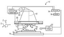
- Substrate 12may be coupled to a substrate chuck 14 .
- Substrate chuck 14may be any chuck including, but not limited to, vacuum, pin-type, groove-type, or electromagnetic, as described in U.S. Pat. No. 6,873,087 entitled “High-Precision Orientation Alignment and Gap Control Stages for Imprint Lithography Processes,” which is incorporated herein by reference.
- Substrate 12 and substrate chuck 14may be supported upon a stage 16 . Further, stage 16 , substrate 12 , and substrate chuck 14 may be positioned on a base (not shown). Stage 16 may provide motion about the x and y axes.
- a template 18Spaced-apart from substrate 12 is a template 18 having a mold 20 extending therefrom towards substrate 20 with a patterning surface 22 thereon.
- mesa 20may be referred to as a mold 20 .
- Mesa 20may also be referred to as a nanoimprint mold 20 .
- template 18may be substantially absent of mold 20 .
- Template 18 and/or mold 20may be formed from such materials including but not limited to, fused-silica, quartz, silicon, organic polymers, siloxane polymers, borosilicate glass, fluorocarbon polymers, metal, and hardened sapphire.
- patterning surface 22comprises features defined by a plurality of spaced-apart recesses 24 and protrusions 26 .
- Template 18may be coupled to a template chuck 28 , template chuck 28 being any chuck including, but not limited to, vacuum, pin-type, groove-type, or electromagnetic, as described in U.S. Pat. No. 6,873,087 entitled “High-Precision Orientation Alignment and Gap Control Stages for Imprint Lithography Processes”.
- Template chuck 28may be coupled to an imprint head 30 to facilitate movement of template 18 and mold 20 .
- System 10further comprises a fluid dispense system 32 .
- Fluid dispense system 32may be in fluid communication with substrate 12 so as to deposit a polymeric material 34 thereon.
- System 10may comprise any number of fluid dispensers and fluid dispense system 32 may comprise a plurality of dispensing units therein.
- Polymeric material 34may be positioned upon substrate 12 using any known technique, e.g., drop dispense, spin-coating, dip coating, chemical vapor deposition (CVD), physical vapor deposition (PVD), thin film deposition, thick film deposition, and the like. As shown, polymeric material 34 may be deposited upon substrate 12 as a plurality of spaced-apart droplets 36 . Typically, polymeric material 34 is disposed upon substrate 12 before the desired volume is defined between mold 20 and substrate 12 . However, polymeric material 34 may fill the volume after the desired volume has been obtained.
- system 10further comprises a source 38 of energy 40 coupled to direct energy 40 along a path 42 .
- Imprint head 30 and stage 16are configured to arrange mold 20 and substrate 12 , respectively, to be in superimposition and disposed in path 42 .
- Either imprint head 30 , stage 16 , or bothvary a distance between mold 20 and substrate 12 to define a desired volume therebetween such that mold 20 contacts polymeric material 34 and the desired volume is filled by polymeric material 34 . More specifically, polymeric material 34 of droplets 36 may ingress and fill recesses 24 of mold 20 .
- source 38produces energy 40 , e.g., broadband ultraviolet radiation that causes polymeric material 34 to solidify and/or cross-link conforming to the shape of a surface 44 of substrate 12 and patterning surface 22 , defining a patterned layer 46 on substrate 12 .
- Patterned layer 46may comprise a residual layer 48 and a plurality of features shown as protrusions 50 and recessions 52 .
- System 10may be regulated by a processor 54 that is in data communication with stage 16 , imprint head 30 , fluid dispense system 32 , and source 38 , operating on a computer readable program stored in memory 56 .
- substrate 12may comprise a plurality of fields, shown as fields a-d. However, in a further embodiment, substrate 12 may comprise any number of fields. Each of fields a-d of substrate 12 may be subjected to the aforementioned patterning process. In a first embodiment, all of fields a-d of substrate 12 may have polymeric material 34 positioned thereon concurrently by fluid dispense system 32 . In a further embodiment, polymeric material 34 may be positioned on fields a-d of substrate 12 sequentially by fluid dispense system 32 . Fields a-d of substrate 12 may have a volume V dispense positioned thereon by fluid dispense system 32 .
- Polymeric material 34 positioned on each of fields a-d of substrate 12may fill the desired volume between mold 20 and substrate 12 , and more specifically, ingress and fill recesses 24 of mold 20 , as described above. Mold 20 may contact polymeric material 34 positioned on each of fields a-d of substrate 12 sequentially.
- mold 20may contact polymeric material 34 positioned on field a of substrate 12 prior to contacting fields b-d of substrate 12 ; mold 20 may contact polymeric material 34 positioned on field b of substrate 12 after contacting field a of substrate 12 and prior to contacting fields c-d of substrate 12 contact mold 20 ; mold 20 may contact polymeric material 34 positioned on field c of substrate 12 after contacting field b of substrate 12 and prior to contacting field d of substrate 12 ; and mold 20 may contact polymeric material 34 positioned on field d of substrate 12 after contacting field c of substrate 12 .
- any desired sequential order of contacting polymeric material 34 on fields a-d of substratemay be employed.
- each of fields a-d of substrate 12may be subjected to differing evaporation times. More specifically, a time between positioning polymeric material 34 on a field a-d of substrate 12 and mold 20 contacting polymeric material 34 on the field a-d of substrate 12 may be referred to as an “evaporation time” of polymeric material 34 positioned on the field a-d of substrate 12 . To that end, a volume of polymeric material 34 positioned on a field a-d of substrate 12 upon contact with mold 20 may differ from a volume of polymeric material 34 positioned on the field a-d of substrate 12 by fluid dispense system 32 .
- polymeric material 34 positioned on field a of substrate 12may have a first evaporation time T a associated therewith resulting in the volume of polymeric material 34 positioned on field a upon contact with mold 20 being V evapA , with V evapA being less than V dispense ; polymeric material 34 positioned on field b of substrate 12 may have a second evaporation time T b associated therewith resulting in the volume of polymeric material 34 positioned on field b upon contact with mold 20 being V evapB , with V evapB being less than V dispense ; polymeric material 34 positioned on field c of substrate 12 may have a third evaporation time T c associated therewith resulting in the volume of polymeric material 34 positioned on field c upon contact with mold 20 being V evapC , with V evapC being less than V dispense ; and polymeric material 34
- evaporation time T bmay be greater than evaporation time T a
- evaporation time T cmay be greater than evaporation time T b
- evaporation time T dmay be greater than evaporation time T c .
- evaporation times T a , T b , T c , and T dmay be defined as follows: T d >T c >T b >T a .
- the volume of polymeric material 34 on the aforementioned second subset of fields a-d of substrate 12 upon contact with mold 20will be greater than the volume of polymeric material 34 on the aforementioned first subset of fields a-d of substrate 12 upon contact with mold 20 .
- volume V evapA of polymeric material 34 on field a of substrate 12 upon contact with mold 20is greater than V evapB of polymeric material 34 on field b of substrate 12 upon contact with mold 20 ; volume V evapB of polymeric material 34 on field b of substrate 12 upon contact with mold 20 is greater than V evapC of polymeric material 34 on field c of substrate 12 upon contact with mold 20 ; and volume V evapC of polymeric material 34 on field c of substrate 12 upon contact with mold 20 is greater than V evapD of polymeric material 34 on field d of substrate 12 upon contact with mold 20 .
- volumes V evapA , V evapB , V evapC , and V evapD , of polymeric material 34 on fields a, b, c, and d, respectively, of substrate 12 , upon contact with mold 20may be defined as follows: V evapA >V evapB >V evapC >V evapD . (2)
- contacting polymeric material 34 positioned on fields a-d of substrate 12 with mold 20 each having a differing volume associated therewithmay result in pattern distortion of features formed from polymeric material 34 in patterned layer 46 ; low fidelity of features form from polymeric material 34 in patterned layer 46 , and a non-uniform thickness of residual layer 48 across patterned layer 46 , all of which are undesirable.
- the volume V dispense positioned on each of fields a-d of substrate 12 by fluid dispense system 32may be varied. More specifically, the volume Of V dispense positioned on the aforementioned first subset of fields a-d of substrate 12 by fluid dispense system 32 may be increased as compared to the volume V dispense positioned on the aforementioned second subset of fields a-d of substrate 12 by fluid dispense system 32 . As a result, upon contact with mold 20 , each of fields a-d of substrate 12 may have substantially the same volume of polymeric material 34 , which may be desired.
- the volume V dispenseD positioned on field d of substrate 12 by fluid dispense system 32is greater than the volume V dispenseC positioned on field c of substrate 12 by fluid dispense system 32 ; the volume V dispenseC positioned on field c of substrate 12 by fluid dispense system 32 is greater than the volume V dispenseB positioned on field b of substrate 12 by fluid dispense system 32 ; and the volume V dispenseB positioned on field b of substrate 12 by fluid dispense system 32 is greater than the volume V dispenseA positioned on field a of substrate 12 by fluid dispense system 32 .
- volumes V dispenseA , V dispenseB , V dispenseC , and V dispenseD , of polymeric material 34 on fields a, b, c, and d, respectively, positioned on substrate 12 by fluid dispense system 32may be defined as follows: V dispenseD >V dispenseC >V dispenseB >V dispenseA (3)
- V dispenseA , V dispenseB , V dispenseC , and V dispenseD of polymeric material 34 positioned on fields a-d of substrate 12respectively, direct imaging of polymeric material 34 in droplets 40 positioned on each field a-d of substrate 12 may be employed.
- film thickness metrology of patterned layer 46may be employed.
- source 38may produce energy 40 to cause polymeric material 34 to be solidified and/or cross-linked, as mentioned above.
- polymeric material 34 positioned on surrounding fields a-d of substrate 12may be concurrently exposed to energy 40 , and thus, may be solidified and/or cross-linked prior to contact with mold 20 , which is undesirable.
- Solidifying and/or cross-linking of polymeric material 34 positioned on the surrounding fields a-d of substrate 12may result in, inter alia, problematic control of the thickness of subsequently disposed layers on the surrounding fields a-d of substrate 12 and formation of deleterious artifacts in layers formed on the surrounding fields a-d of substrate 12 , all of which are undesirable.
- a method of patterning substrate 12 to minimize, if not prevent, undesired curing and/or cross-linking of polymeric material 32 on surrounding fields a-d of substrate 12is described further below.
- substrate 12is shown have a plurality of fields w-z.
- Each field w-z of substrate 12comprises a plurality of sub-fields, i.e., field w of substrate 12 comprises sub-fields w 1 -w 4 ; field x of substrate 12 comprises sub-fields x 1 -x 4 ; field y of substrate 12 comprises sub-fields y 1 -y 4 ; and field z of substrate 12 comprises sub-fields z 1 -z 4 .
- Each sub-field of a field w-z of substrate 12may be spaced-apart from the remaining sub-fields of the field w-z of substrate 12 by the remaining fields w-z of substrate 12 .
- each sub-field w 1 -w 4 of field w of substrate 12may be separated from the remaining sub-fields w 1 -w 4 of field w of substrate 12 by fields x-z; each sub-field x 1 -x 4 of field x of substrate 12 may be separated from the remaining sub-fields x 1 -x 4 of field x of substrate 12 by fields w, y, and z; each sub-field y 1 -y 4 of field y of substrate 12 may be separated from the remaining sub-fields y 1 -y 4 of field y of substrate 12 by fields w, x, and z; and each sub-field z 1 -z 4 of field z of substrate 12 may be separated from the remaining sub-fields z 1 -z 4 of field z of substrate 12 by fields w-y.
- polymeric material 34may be positioned on field w using any of the techniques mentioned above.
- Polymeric material 28may be positioned on field w concurrently by fluid dispense system 32 , or in a further embodiment, polymeric material 34 may be positioned on sub-fields w 1 -w 4 of field w of substrate 12 sequentially by fluid dispense system 32 .
- mold 20may contact polymeric material 34 positioned on each sub-field w 1 -w 4 of field w of substrate 12 .
- Mold 20may contact polymeric material 34 positioned on sub-field w 1 of substrate 12 prior to contacting sub-fields w 2 -w 4 of substrate 12 , with polymeric material 34 on sub-field w 1 of substrate 12 being subsequently solidified or cross-linked;
- mold 20may contact polymeric material 34 positioned on sub-field w 2 of substrate 12 after contacting sub-field w 1 of substrate 12 and prior to contacting sub-fields w 3 -w 4 of substrate 12 with polymeric material 34 on sub-field w 2 of substrate 12 being subsequently solidified or cross-linked;
- mold 20may contact polymeric material 34 positioned on sub-field w 3 of substrate 12 after contacting sub-field w 2 of substrate 12 and prior to contacting sub-field w 4 of substrate 12 with polymeric material 34 on sub-field w 3 of substrate 12 being subsequently solid
- polymeric material 34may be positioned on field x using any of the techniques mentioned above.
- Polymeric material 28may be positioned on field x concurrently by fluid dispense system 32 , or in a further embodiment, polymeric material 34 may be positioned on sub-fields x 1 -x 4 of field x of substrate 12 sequentially by fluid dispense system 32 .
- mold 20may contact polymeric material 34 positioned on each sub-field x 1 -x 4 of field x of substrate 12 .
- Mold 20may contact polymeric material 34 positioned on sub-field x 1 of substrate 12 prior to contacting sub-fields x 2 -x 4 of substrate 12 , with polymeric material 34 on sub-field x 1 of substrate 12 being subsequently solidified or cross-linked;
- mold 20may contact polymeric material 34 positioned on sub-field x 2 of substrate 12 after contacting sub-field x 1 of substrate 12 and prior to contacting sub-fields x 3 -x 4 of substrate 12 with polymeric material 34 on sub-field x 2 of substrate 12 being subsequently solidified or cross-linked;
- mold 20may contact polymeric material 34 positioned on sub-field x 3 of substrate 12 after contacting sub-field x 2 of substrate 12 and prior to contacting sub-field x 4 of substrate 12 with polymeric material 34 on sub-field x 3 of substrate 12 being subsequently solid
- polymeric material 34may be positioned on field y using any of the techniques mentioned above.
- Polymeric material 28may be positioned on field y concurrently by fluid dispense system 32 , or in a further embodiment, polymeric material 34 may be positioned on sub-fields y 1 -y 4 of field y of substrate 12 sequentially by fluid dispense system 32 .
- mold 20may contact polymeric material 34 positioned on each sub-field y 1 -y 4 of field y of substrate 12 .
- Mold 20may contact polymeric material 34 positioned on sub-field y 1 of substrate 12 prior to contacting sub-fields y 2 -y 4 of substrate 12 , with polymeric material 34 on sub-field y 1 of substrate 12 being subsequently solidified or cross-linked;
- mold 20may contact polymeric material 34 positioned on sub-field y 2 of substrate 12 after contacting sub-field y 1 of substrate 12 and prior to contacting sub-fields y 3 -y 4 of substrate 12 with polymeric material 34 on sub-field y 2 of substrate 12 being subsequently solidified or cross-linked;
- mold 20may contact polymeric material 34 positioned on sub-field y 3 of substrate 12 after contacting sub-field y 2 of substrate 12 and prior to contacting sub-field y 4 of substrate 12 with polymeric material 34 on sub-field y 3 of substrate 12 being subsequently solidified
- polymeric material 34may be positioned on field z using any of the techniques mentioned above.
- Polymeric material 28may be positioned on field z concurrently by fluid dispense system 32 , or in a further embodiment, polymeric material 34 may be positioned on sub-fields z 1 -z 4 of field w of substrate 12 sequentially by fluid dispense system 32 .
- mold 20may contact polymeric material 34 positioned on each sub-field z 1 -z 4 of field z of substrate 12 .
- Mold 20may contact polymeric material 34 positioned on sub-field z 1 of substrate 12 prior to contacting sub-fields z 2 -z 4 of substrate 12 , with polymeric material 34 on sub-field z 1 of substrate 12 being subsequently solidified or cross-linked;
- mold 20may contact polymeric material 34 positioned on sub-field z 2 of substrate 12 after contacting sub-field z 1 of substrate 12 and prior to contacting sub-fields z 3 -z 4 of substrate 12 with polymeric material 34 on sub-field z 2 of substrate 12 being subsequently solidified or cross-linked;
- mold 20may contact polymeric material 34 positioned on sub-field z 3 of substrate 12 after contacting sub-field z 2 of substrate 12 and prior to contacting sub-field z 4 of substrate 12 with polymeric material 34 on sub-field z 3 of substrate 12 being subsequently solid
Landscapes
- Engineering & Computer Science (AREA)
- Chemical & Material Sciences (AREA)
- Nanotechnology (AREA)
- Physics & Mathematics (AREA)
- Manufacturing & Machinery (AREA)
- General Physics & Mathematics (AREA)
- Crystallography & Structural Chemistry (AREA)
- Theoretical Computer Science (AREA)
- Mathematical Physics (AREA)
- Microelectronics & Electronic Packaging (AREA)
- Condensed Matter Physics & Semiconductors (AREA)
- Mechanical Engineering (AREA)
- Exposure Of Semiconductors, Excluding Electron Or Ion Beam Exposure (AREA)
- Micromachines (AREA)
- Shaping Of Tube Ends By Bending Or Straightening (AREA)
Abstract
Description
Td>Tc>Tb>Ta. (1)
VevapA>VevapB>VevapC>VevapD. (2)
VdispenseD>VdispenseC>VdispenseB>VdispenseA (3)
Claims (21)
Priority Applications (1)
| Application Number | Priority Date | Filing Date | Title |
|---|---|---|---|
| US11/692,450US8142850B2 (en) | 2006-04-03 | 2007-03-28 | Patterning a plurality of fields on a substrate to compensate for differing evaporation times |
Applications Claiming Priority (2)
| Application Number | Priority Date | Filing Date | Title |
|---|---|---|---|
| US78878206P | 2006-04-03 | 2006-04-03 | |
| US11/692,450US8142850B2 (en) | 2006-04-03 | 2007-03-28 | Patterning a plurality of fields on a substrate to compensate for differing evaporation times |
Publications (2)
| Publication Number | Publication Date |
|---|---|
| US20070231981A1 US20070231981A1 (en) | 2007-10-04 |
| US8142850B2true US8142850B2 (en) | 2012-03-27 |
Family
ID=38610072
Family Applications (1)
| Application Number | Title | Priority Date | Filing Date |
|---|---|---|---|
| US11/692,450Active2029-07-08US8142850B2 (en) | 2006-04-03 | 2007-03-28 | Patterning a plurality of fields on a substrate to compensate for differing evaporation times |
Country Status (5)
| Country | Link |
|---|---|
| US (1) | US8142850B2 (en) |
| JP (1) | JP5084823B2 (en) |
| KR (1) | KR101299475B1 (en) |
| TW (1) | TWI339159B (en) |
| WO (1) | WO2007120537A2 (en) |
Cited By (7)
| Publication number | Priority date | Publication date | Assignee | Title |
|---|---|---|---|---|
| US20110057354A1 (en)* | 2009-09-10 | 2011-03-10 | Canon Kabushiki Kaisha | Imprinting method and imprinting apparatus |
| US9811671B1 (en) | 2000-05-24 | 2017-11-07 | Copilot Ventures Fund Iii Llc | Authentication method and system |
| US9846814B1 (en) | 2008-04-23 | 2017-12-19 | Copilot Ventures Fund Iii Llc | Authentication method and system |
| US11017993B2 (en)* | 2017-03-16 | 2021-05-25 | Bruker Daltonik Gmbh | Separation of liquid in droplets and sedimented material enclosed therein |
| US11054741B2 (en) | 2017-09-19 | 2021-07-06 | Canon Kabushiki Kaisha | Imprint apparatus and method of manufacturing article |
| US11376766B2 (en) | 2018-08-09 | 2022-07-05 | Canon Kabushiki Kaisha | Pattern forming method |
| US12174531B2 (en) | 2019-12-04 | 2024-12-24 | Canon Kabushiki Kaisha | Imprint apparatus, imprint method, and method of manufacturing article |
Families Citing this family (28)
| Publication number | Priority date | Publication date | Assignee | Title |
|---|---|---|---|---|
| US7179079B2 (en)* | 2002-07-08 | 2007-02-20 | Molecular Imprints, Inc. | Conforming template for patterning liquids disposed on substrates |
| US7442336B2 (en)* | 2003-08-21 | 2008-10-28 | Molecular Imprints, Inc. | Capillary imprinting technique |
| US7019819B2 (en) | 2002-11-13 | 2006-03-28 | Molecular Imprints, Inc. | Chucking system for modulating shapes of substrates |
| US7906058B2 (en) | 2005-12-01 | 2011-03-15 | Molecular Imprints, Inc. | Bifurcated contact printing technique |
| MY144847A (en) | 2005-12-08 | 2011-11-30 | Molecular Imprints Inc | Method and system for double-sided patterning of substrates |
| US7670530B2 (en) | 2006-01-20 | 2010-03-02 | Molecular Imprints, Inc. | Patterning substrates employing multiple chucks |
| US7802978B2 (en)* | 2006-04-03 | 2010-09-28 | Molecular Imprints, Inc. | Imprinting of partial fields at the edge of the wafer |
| US8012395B2 (en) | 2006-04-18 | 2011-09-06 | Molecular Imprints, Inc. | Template having alignment marks formed of contrast material |
| US7547398B2 (en) | 2006-04-18 | 2009-06-16 | Molecular Imprints, Inc. | Self-aligned process for fabricating imprint templates containing variously etched features |
| US8707890B2 (en) | 2006-07-18 | 2014-04-29 | Asml Netherlands B.V. | Imprint lithography |
| JP4908369B2 (en)* | 2007-10-02 | 2012-04-04 | 株式会社東芝 | Imprint method and imprint system |
| US8012394B2 (en)* | 2007-12-28 | 2011-09-06 | Molecular Imprints, Inc. | Template pattern density doubling |
| US8361371B2 (en)* | 2008-02-08 | 2013-01-29 | Molecular Imprints, Inc. | Extrusion reduction in imprint lithography |
| US20090212012A1 (en)* | 2008-02-27 | 2009-08-27 | Molecular Imprints, Inc. | Critical dimension control during template formation |
| TW201022017A (en)* | 2008-09-30 | 2010-06-16 | Molecular Imprints Inc | Particle mitigation for imprint lithography |
| US8529778B2 (en)* | 2008-11-13 | 2013-09-10 | Molecular Imprints, Inc. | Large area patterning of nano-sized shapes |
| JP5744422B2 (en)* | 2010-06-17 | 2015-07-08 | キヤノン株式会社 | Imprint method, imprint apparatus, sample shot extraction method, and article manufacturing method using the same |
| KR102046933B1 (en) | 2010-11-05 | 2019-11-20 | 캐논 나노테크놀로지즈 인코퍼레이티드 | Patterning of non-convex shaped nanostructures |
| JP5275419B2 (en)* | 2011-08-08 | 2013-08-28 | 株式会社東芝 | Pattern formation method |
| JP7041483B2 (en)* | 2017-09-22 | 2022-03-24 | キヤノン株式会社 | Imprint method, imprint device, and manufacturing method of goods |
| KR102527567B1 (en)* | 2018-02-23 | 2023-05-03 | 에스케이하이닉스 주식회사 | Method of forming imprinted patterns for suppressing template damages from particles |
| JP2021027107A (en) | 2019-08-01 | 2021-02-22 | キヤノン株式会社 | Imprint apparatus, imprint method, and article manufacturing method |
| JP7362429B2 (en)* | 2019-10-31 | 2023-10-17 | キヤノン株式会社 | Molding equipment, molding method, and article manufacturing method |
| JP7401267B2 (en) | 2019-11-12 | 2023-12-19 | キヤノン株式会社 | Imprint device and imprint device control method |
| JP7337670B2 (en) | 2019-11-15 | 2023-09-04 | キヤノン株式会社 | IMPRINT APPARATUS, IMPRINT METHOD, AND ARTICLE MANUFACTURING METHOD |
| JP7508285B2 (en) | 2020-06-22 | 2024-07-01 | キヤノン株式会社 | Pattern forming method, imprint apparatus, and article manufacturing method |
| US11474441B2 (en) | 2020-06-25 | 2022-10-18 | Canon Kabushiki Kaisha | Systems and methods for generating drop patterns |
| US12282252B2 (en) | 2023-02-21 | 2025-04-22 | Canon Kabushiki Kaisha | Systems, devices, and methods for generating drop patterns |
Citations (266)
| Publication number | Priority date | Publication date | Assignee | Title |
|---|---|---|---|---|
| US1000000A (en) | 1910-04-25 | 1911-08-08 | Francis H Holton | Vehicle-tire. |
| US1236304A (en) | 1917-02-03 | 1917-08-07 | Riley L Howell | Cushioned hand-stamp. |
| US2000000A (en) | 1932-05-12 | 1935-04-30 | Budd Edward G Mfg Co | Vehicle wheel construction |
| US3000000A (en) | 1955-05-06 | 1961-09-12 | Gen Electric | Automatic reading system |
| US3503538A (en) | 1966-11-29 | 1970-03-31 | Bp Chem Int Ltd | Metering process and apparatus |
| US3781214A (en) | 1970-11-25 | 1973-12-25 | Dainippon Ink & Chemicals | Photopolymerizable printing ink |
| US4022855A (en) | 1975-03-17 | 1977-05-10 | Eastman Kodak Company | Method for making a plastic optical element having a gradient index of refraction |
| US4070116A (en) | 1975-06-23 | 1978-01-24 | International Business Machines Corporation | Gap measuring device for defining the distance between two or more surfaces |
| US4208240A (en) | 1979-01-26 | 1980-06-17 | Gould Inc. | Method and apparatus for controlling plasma etching |
| US4364971A (en) | 1980-06-18 | 1982-12-21 | Felix Schoeller, Jr. Gmbh & Co. | Waterproof photographic paper and method of producing same |
| US4440804A (en) | 1982-08-02 | 1984-04-03 | Fairchild Camera & Instrument Corporation | Lift-off process for fabricating self-aligned contacts |
| US4512848A (en) | 1984-02-06 | 1985-04-23 | Exxon Research And Engineering Co. | Procedure for fabrication of microstructures over large areas using physical replication |
| US4521445A (en) | 1982-09-07 | 1985-06-04 | Energy Sciences, Inc. | Method and apparatus for electron curing on a cooled drum |
| US4552832A (en) | 1982-03-06 | 1985-11-12 | Braun Aktiengesellschaft | Shear foil having protrusions on its skin-contacting surface thereof |
| US4576900A (en) | 1981-10-09 | 1986-03-18 | Amdahl Corporation | Integrated circuit multilevel interconnect system and method |
| US4637904A (en) | 1983-11-14 | 1987-01-20 | Rohm And Haas Company | Process for molding a polymeric layer onto a substrate |
| US4676868A (en) | 1986-04-23 | 1987-06-30 | Fairchild Semiconductor Corporation | Method for planarizing semiconductor substrates |
| US4707218A (en) | 1986-10-28 | 1987-11-17 | International Business Machines Corporation | Lithographic image size reduction |
| US4731155A (en) | 1987-04-15 | 1988-03-15 | General Electric Company | Process for forming a lithographic mask |
| US4737425A (en) | 1986-06-10 | 1988-04-12 | International Business Machines Corporation | Patterned resist and process |
| US4848911A (en) | 1986-06-11 | 1989-07-18 | Kabushiki Kaisha Toshiba | Method for aligning first and second objects, relative to each other, and apparatus for practicing this method |
| US4857477A (en) | 1986-09-18 | 1989-08-15 | Oki Electric Industry Co., Ltd. | Process for fabricating a semiconductor device |
| US4862019A (en) | 1988-04-20 | 1989-08-29 | Texas Instruments Incorporated | Single-level poly programmable bit circuit |
| US4866307A (en) | 1988-04-20 | 1989-09-12 | Texas Instruments Incorporated | Integrated programmable bit circuit using single-level poly construction |
| US4908298A (en) | 1985-03-19 | 1990-03-13 | International Business Machines Corporation | Method of creating patterned multilayer films for use in production of semiconductor circuits and systems |
| US4909151A (en) | 1986-11-10 | 1990-03-20 | Matsushita Electric Industrial Co., Ltd. | Method of forming an ink image and printing the formed image |
| US4919748A (en) | 1989-06-30 | 1990-04-24 | At&T Bell Laboratories | Method for tapered etching |
| US4921778A (en) | 1988-07-29 | 1990-05-01 | Shipley Company Inc. | Photoresist pattern fabrication employing chemically amplified metalized material |
| US4932358A (en) | 1989-05-18 | 1990-06-12 | Genus, Inc. | Perimeter wafer seal |
| US4936465A (en) | 1987-12-07 | 1990-06-26 | Zoeld Tibor | Method and apparatus for fast, reliable, and environmentally safe dispensing of fluids, gases and individual particles of a suspension through pressure control at well defined parts of a closed flow-through system |
| US4957663A (en) | 1986-02-13 | 1990-09-18 | U.S. Philips Corp. | Method of manufacturing optical components |
| US4959252A (en) | 1986-09-29 | 1990-09-25 | Rhone-Poulenc Chimie | Highly oriented thermotropic optical disc member |
| US4964945A (en) | 1988-12-09 | 1990-10-23 | Minnesota Mining And Manufacturing Company | Lift off patterning process on a flexible substrate |
| US4980316A (en) | 1988-07-20 | 1990-12-25 | Siemens Aktiengesellschaft | Method for producing a resist structure on a semiconductor |
| US5003062A (en) | 1990-04-19 | 1991-03-26 | Taiwan Semiconductor Manufacturing Co. | Semiconductor planarization process for submicron devices |
| US5028361A (en) | 1987-11-09 | 1991-07-02 | Takeo Fujimoto | Method for molding a photosensitive composition |
| US5028366A (en) | 1988-01-12 | 1991-07-02 | Air Products And Chemicals, Inc. | Water based mold release compositions for making molded polyurethane foam |
| US5053318A (en) | 1989-05-18 | 1991-10-01 | Shipley Company Inc. | Plasma processing with metal mask integration |
| US5073230A (en) | 1990-04-17 | 1991-12-17 | Arizona Board Of Regents Acting On Behalf Of Arizona State University | Means and methods of lifting and relocating an epitaxial device layer |
| US5110514A (en) | 1989-05-01 | 1992-05-05 | Soane Technologies, Inc. | Controlled casting of a shrinkable material |
| US5124089A (en) | 1986-12-25 | 1992-06-23 | Sony Corporation | Method of producing transmissive screens |
| US5126006A (en) | 1990-10-30 | 1992-06-30 | International Business Machines Corp. | Plural level chip masking |
| US5148037A (en) | 1988-09-09 | 1992-09-15 | Canon Kabushiki Kaisha | Position detecting method and apparatus |
| US5151754A (en) | 1989-10-06 | 1992-09-29 | Kabushiki Kaisha Toshiba | Method and an apparatus for measuring a displacement between two objects and a method and an apparatus for measuring a gap distance between two objects |
| FR2677043A1 (en) | 1991-05-29 | 1992-12-04 | Solems Sa | Process, device and apparatus for treating a substrate with a low-pressure plasma |
| US5212147A (en) | 1991-05-15 | 1993-05-18 | Hewlett-Packard Company | Method of forming a patterned in-situ high Tc superconductive film |
| US5232874A (en) | 1992-06-22 | 1993-08-03 | Micron Technology, Inc. | Method for producing a semiconductor wafer having shallow and deep buried contacts |
| US5240878A (en) | 1991-04-26 | 1993-08-31 | International Business Machines Corporation | Method for forming patterned films on a substrate |
| US5240550A (en) | 1990-09-21 | 1993-08-31 | U.S. Philips Corp. | Method of forming at least one groove in a substrate layer |
| US5244818A (en) | 1992-04-08 | 1993-09-14 | Georgia Tech Research Corporation | Processes for lift-off of thin film materials and for the fabrication of three dimensional integrated circuits |
| US5246880A (en) | 1992-04-27 | 1993-09-21 | Eastman Kodak Company | Method for creating substrate electrodes for flip chip and other applications |
| US5250472A (en) | 1992-09-03 | 1993-10-05 | Industrial Technology Research Institute | Spin-on-glass integration planarization having siloxane partial etchback and silicate processes |
| US5259926A (en) | 1991-09-24 | 1993-11-09 | Hitachi, Ltd. | Method of manufacturing a thin-film pattern on a substrate |
| US5277749A (en) | 1991-10-17 | 1994-01-11 | International Business Machines Corporation | Methods and apparatus for relieving stress and resisting stencil delamination when performing lift-off processes that utilize high stress metals and/or multiple evaporation steps |
| US5288436A (en) | 1990-11-06 | 1994-02-22 | Colloptics, Inc. | Methods of fabricating a collagen lenticule precursor for modifying the cornea |
| US5320273A (en)* | 1993-08-02 | 1994-06-14 | Ford Motor Company | Gas flow distribution system for molten solder dispensing process |
| US5324683A (en) | 1993-06-02 | 1994-06-28 | Motorola, Inc. | Method of forming a semiconductor structure having an air region |
| US5328810A (en) | 1990-05-07 | 1994-07-12 | Micron Technology, Inc. | Method for reducing, by a factor or 2-N, the minimum masking pitch of a photolithographic process |
| US5330881A (en) | 1989-06-02 | 1994-07-19 | Digital Equipment Corp. | Microlithographic method for producing thick, vertically-walled photoresist patterns |
| US5357122A (en) | 1991-09-05 | 1994-10-18 | Sony Corporation | Three-dimensional optical-electronic integrated circuit device with raised sections |
| US5362606A (en) | 1989-10-18 | 1994-11-08 | Massachusetts Institute Of Technology | Positive resist pattern formation through focused ion beam exposure and surface barrier silylation |
| US5362940A (en) | 1990-11-09 | 1994-11-08 | Litel Instruments | Use of Fresnel zone plates for material processing |
| US5364222A (en) | 1992-02-05 | 1994-11-15 | Tokyo Electron Limited | Apparatus for processing wafer-shaped substrates |
| US5366851A (en) | 1991-07-23 | 1994-11-22 | At&T Bell Laboratories | Device fabrication process |
| US5371822A (en) | 1992-06-09 | 1994-12-06 | Digital Equipment Corporation | Method of packaging and assembling opto-electronic integrated circuits |
| US5374327A (en) | 1992-04-28 | 1994-12-20 | Tokyo Electron Limited | Plasma processing method |
| US5376810A (en) | 1992-06-26 | 1994-12-27 | California Institute Of Technology | Growth of delta-doped layers on silicon CCD/S for enhanced ultraviolet response |
| US5422295A (en) | 1992-12-10 | 1995-06-06 | Samsung Electronics Co., Ltd. | Method for forming a semiconductor memory device having a vertical multi-layered storage electrode |
| US5424549A (en) | 1991-12-20 | 1995-06-13 | Board Of Supervisors Of Louisiana State University And Agricultural And Mechanical College | Scanning systems for high resolution e-beam and X-ray lithography |
| US5425848A (en) | 1993-03-16 | 1995-06-20 | U.S. Philips Corporation | Method of providing a patterned relief of cured photoresist on a flat substrate surface and device for carrying out such a method |
| US5431777A (en) | 1992-09-17 | 1995-07-11 | International Business Machines Corporation | Methods and compositions for the selective etching of silicon |
| US5434107A (en) | 1994-01-28 | 1995-07-18 | Texas Instruments Incorporated | Method for planarization |
| US5445195A (en) | 1992-07-15 | 1995-08-29 | Kim; Dae S. | Automatic computer-controlled liquid dispenser |
| US5449117A (en) | 1993-10-04 | 1995-09-12 | Technical Concepts, L.P. | Apparatus and method for controllably dispensing drops of liquid |
| US5451435A (en) | 1990-06-18 | 1995-09-19 | At&T Corp. | Method for forming dielectric |
| US5453157A (en) | 1994-05-16 | 1995-09-26 | Texas Instruments Incorporated | Low temperature anisotropic ashing of resist for semiconductor fabrication |
| US5458520A (en) | 1994-12-13 | 1995-10-17 | International Business Machines Corporation | Method for producing planar field emission structure |
| US5468542A (en) | 1985-12-23 | 1995-11-21 | General Electric Company | Method for production of a coated substrate with controlled surface characteristics |
| US5480047A (en) | 1993-06-04 | 1996-01-02 | Sharp Kabushiki Kaisha | Method for forming a fine resist pattern |
| US5512131A (en) | 1993-10-04 | 1996-04-30 | President And Fellows Of Harvard College | Formation of microstamped patterns on surfaces and derivative articles |
| US5542605A (en) | 1994-04-07 | 1996-08-06 | Flow-Rite Controls, Ltd. | Automatic liquid dispenser |
| US5545367A (en) | 1992-04-15 | 1996-08-13 | Soane Technologies, Inc. | Rapid prototype three dimensional stereolithography |
| US5601641A (en) | 1992-07-21 | 1997-02-11 | Tse Industries, Inc. | Mold release composition with polybutadiene and method of coating a mold core |
| US5612068A (en) | 1994-03-14 | 1997-03-18 | Leybold Aktiengesellschaft | Apparatus for the transfer of substrates |
| US5628917A (en) | 1995-02-03 | 1997-05-13 | Cornell Research Foundation, Inc. | Masking process for fabricating ultra-high aspect ratio, wafer-free micro-opto-electromechanical structures |
| US5643364A (en) | 1994-11-30 | 1997-07-01 | Applied Materials, Inc. | Plasma chamber with fixed RF matching |
| US5654238A (en) | 1995-08-03 | 1997-08-05 | International Business Machines Corporation | Method for etching vertical contact holes without substrate damage caused by directional etching |
| US5669303A (en) | 1996-03-04 | 1997-09-23 | Motorola | Apparatus and method for stamping a surface |
| US5723176A (en) | 1994-03-02 | 1998-03-03 | Telecommunications Research Laboratories | Method and apparatus for making optical components by direct dispensing of curable liquid |
| US5736424A (en) | 1987-02-27 | 1998-04-07 | Lucent Technologies Inc. | Device fabrication involving planarization |
| US5753014A (en) | 1993-11-12 | 1998-05-19 | Van Rijn; Cornelis Johannes Maria | Membrane filter and a method of manufacturing the same as well as a membrane |
| US5772905A (en) | 1995-11-15 | 1998-06-30 | Regents Of The University Of Minnesota | Nanoimprint lithography |
| US5776748A (en) | 1993-10-04 | 1998-07-07 | President And Fellows Of Harvard College | Method of formation of microstamped patterns on plates for adhesion of cells and other biological materials, devices and uses therefor |
| US5804474A (en) | 1996-04-10 | 1998-09-08 | Murata Manufacturing Co., Ltd. | Method for forming a V-shaped gate electrode in a semiconductor device, and the structure of the electrode |
| US5812629A (en) | 1997-04-30 | 1998-09-22 | Clauser; John F. | Ultrahigh resolution interferometric x-ray imaging |
| US5817579A (en) | 1997-04-09 | 1998-10-06 | Vanguard International Semiconductor Corporation | Two step plasma etch method for forming self aligned contact |
| US5820769A (en) | 1995-05-24 | 1998-10-13 | Regents Of The University Of Minnesota | Method for making magnetic storage having discrete elements with quantized magnetic moments |
| US5843363A (en) | 1995-03-31 | 1998-12-01 | Siemens Aktiengesellschaft | Ablation patterning of multi-layered structures |
| US5849209A (en) | 1995-03-31 | 1998-12-15 | Johnson & Johnson Vision Products, Inc. | Mold material made with additives |
| US5849222A (en) | 1995-09-29 | 1998-12-15 | Johnson & Johnson Vision Products, Inc. | Method for reducing lens hole defects in production of contact lens blanks |
| US5858580A (en) | 1997-09-17 | 1999-01-12 | Numerical Technologies, Inc. | Phase shifting circuit manufacture method and apparatus |
| US5888650A (en) | 1996-06-03 | 1999-03-30 | Minnesota Mining And Manufacturing Company | Temperature-responsive adhesive article |
| US5895263A (en) | 1996-12-19 | 1999-04-20 | International Business Machines Corporation | Process for manufacture of integrated circuit device |
| US5900160A (en) | 1993-10-04 | 1999-05-04 | President And Fellows Of Harvard College | Methods of etching articles via microcontact printing |
| US5907782A (en) | 1998-08-15 | 1999-05-25 | Acer Semiconductor Manufacturing Inc. | Method of forming a multiple fin-pillar capacitor for a high density dram cell |
| US5926690A (en) | 1997-05-28 | 1999-07-20 | Advanced Micro Devices, Inc. | Run-to-run control process for controlling critical dimensions |
| US5948470A (en) | 1997-04-28 | 1999-09-07 | Harrison; Christopher | Method of nanoscale patterning and products made thereby |
| US5948570A (en) | 1995-05-26 | 1999-09-07 | Lucent Technologies Inc. | Process for dry lithographic etching |
| US5974150A (en) | 1997-09-30 | 1999-10-26 | Tracer Detection Technology Corp. | System and method for authentication of goods |
| US5983906A (en) | 1997-01-24 | 1999-11-16 | Applied Materials, Inc. | Methods and apparatus for a cleaning process in a high temperature, corrosive, plasma environment |
| US6027595A (en) | 1998-07-02 | 2000-02-22 | Samsung Electronics Co., Ltd. | Method of making optical replicas by stamping in photoresist and replicas formed thereby |
| US6046056A (en) | 1996-06-28 | 2000-04-04 | Caliper Technologies Corporation | High throughput screening assay systems in microscale fluidic devices |
| US6048623A (en) | 1996-12-18 | 2000-04-11 | Kimberly-Clark Worldwide, Inc. | Method of contact printing on gold coated films |
| US6048799A (en) | 1987-02-27 | 2000-04-11 | Lucent Technologies Inc. | Device fabrication involving surface planarization |
| US6067144A (en) | 1996-10-23 | 2000-05-23 | Kabushiki Kaisha Toshiba | LCD cell having two supporting gap members different in height |
| US6074827A (en) | 1996-07-30 | 2000-06-13 | Aclara Biosciences, Inc. | Microfluidic method for nucleic acid purification and processing |
| US6089853A (en) | 1997-12-24 | 2000-07-18 | International Business Machines Corporation | Patterning device for patterning a substrate with patterning cavities fed by service cavities |
| US6150680A (en) | 1998-03-05 | 2000-11-21 | Welch Allyn, Inc. | Field effect semiconductor device having dipole barrier |
| US6180239B1 (en) | 1993-10-04 | 2001-01-30 | President And Fellows Of Harvard College | Microcontact printing on surfaces and derivative articles |
| US6218316B1 (en) | 1998-10-22 | 2001-04-17 | Micron Technology, Inc. | Planarization of non-planar surfaces in device fabrication |
| US6242363B1 (en) | 1999-08-11 | 2001-06-05 | Adc Telecommunications, Inc. | Method of etching a wafer layer using a sacrificial wall to form vertical sidewall |
| US6245213B1 (en) | 1996-09-06 | 2001-06-12 | Obducat Ab | Method for anisotropic etching of structures in conducting materials |
| US20010008310A1 (en)* | 1999-12-27 | 2001-07-19 | Fujitsu Limited | Method for forming bumps, semiconductor device, and solder paste |
| US6274294B1 (en) | 1999-02-03 | 2001-08-14 | Electroformed Stents, Inc. | Cylindrical photolithography exposure process and apparatus |
| US6279474B1 (en) | 1993-08-13 | 2001-08-28 | Heidelberger Druckmaschinen Ag | Method and device for transferring ink in a printing unit of an offset printing press |
| US6306467B1 (en) | 1999-06-14 | 2001-10-23 | Ford Global Technologies, Inc. | Method of solid free form fabrication of objects |
| US6309580B1 (en) | 1995-11-15 | 2001-10-30 | Regents Of The University Of Minnesota | Release surfaces, particularly for use in nanoimprint lithography |
| US6326627B1 (en) | 2000-08-02 | 2001-12-04 | Archimedes Technology Group, Inc. | Mass filtering sputtered ion source |
| US6329256B1 (en) | 1999-09-24 | 2001-12-11 | Advanced Micro Devices, Inc. | Self-aligned damascene gate formation with low gate resistance |
| US6334960B1 (en) | 1999-03-11 | 2002-01-01 | Board Of Regents, The University Of Texas System | Step and flash imprint lithography |
| US6337262B1 (en) | 2000-03-06 | 2002-01-08 | Chartered Semiconductor Manufacturing Ltd. | Self aligned T-top gate process integration |
| US6348999B1 (en) | 1995-05-10 | 2002-02-19 | Epigem Limited | Micro relief element and preparation thereof |
| US6355198B1 (en) | 1996-03-15 | 2002-03-12 | President And Fellows Of Harvard College | Method of forming articles including waveguides via capillary micromolding and microtransfer molding |
| US20020038916A1 (en) | 1998-12-23 | 2002-04-04 | 3M Innovative Properties Company | Method for precise molding and alignment of structures on a substrate using a stretchable mold |
| US20020042027A1 (en) | 1998-10-09 | 2002-04-11 | Chou Stephen Y. | Microscale patterning and articles formed thereby |
| US6376379B1 (en) | 2000-02-01 | 2002-04-23 | Chartered Semiconductor Manufacturing Ltd. | Method of hard mask patterning |
| US6383928B1 (en) | 1999-09-02 | 2002-05-07 | Texas Instruments Incorporated | Post copper CMP clean |
| US6387330B1 (en) | 2000-04-12 | 2002-05-14 | George Steven Bova | Method and apparatus for storing and dispensing reagents |
| US6388253B1 (en) | 1999-06-29 | 2002-05-14 | Applied Materials, Inc. | Integrated critical dimension control for semiconductor device manufacturing |
| US6387783B1 (en) | 1999-04-26 | 2002-05-14 | International Business Machines Corporation | Methods of T-gate fabrication using a hybrid resist |
| US6391217B2 (en) | 1999-12-23 | 2002-05-21 | University Of Massachusetts | Methods and apparatus for forming submicron patterns on films |
| US6391798B1 (en) | 1987-02-27 | 2002-05-21 | Agere Systems Guardian Corp. | Process for planarization a semiconductor substrate |
| US20020094496A1 (en) | 2000-07-17 | 2002-07-18 | Choi Byung J. | Method and system of automatic fluid dispensing for imprint lithography processes |
| US6423207B1 (en) | 1998-03-05 | 2002-07-23 | Obducat Ab | Method and apparatus for etching |
| US20020110992A1 (en) | 2001-02-12 | 2002-08-15 | Lam Research Corporation | Use of hydrocarbon addition for the elimination of micromasking during etching |
| US20020111036A1 (en) | 2001-02-12 | 2002-08-15 | Lam Research Corporation | Unique process chemistry for etching organic low-k materials |
| US20020116857A1 (en) | 2001-02-23 | 2002-08-29 | Franz Wonisch | Firearm |
| US20020122873A1 (en) | 2000-01-05 | 2002-09-05 | Mirkin Chad A. | Nanolithography methods and products therefor and produced thereby |
| US20020132482A1 (en) | 2000-07-18 | 2002-09-19 | Chou Stephen Y. | Fluid pressure imprint lithography |
| US20020170880A1 (en) | 2001-03-22 | 2002-11-21 | Yong Chen | Scanning probe based lithographic alignment |
| US6495907B1 (en) | 1994-09-30 | 2002-12-17 | Texas Instruments Incorporated | Conductor reticulation for improved device planarity |
| US20020191141A1 (en) | 2001-06-14 | 2002-12-19 | Bing-Jei Liao | Panel with a blocker for separating sealant and liquid crystal layer |
| US6498640B1 (en) | 1999-12-30 | 2002-12-24 | Koninklijke Philips Electronics N.V. | Method to measure alignment using latent image grating structures |
| US6503829B2 (en) | 2000-08-19 | 2003-01-07 | Samsung Electronics Co., Ltd. | Metal via contact of a semiconductor device and method for fabricating the same |
| US6514672B2 (en) | 1999-06-17 | 2003-02-04 | Taiwan Semiconductor Manufacturing Company | Dry development process for a bi-layer resist system |
| US20030025895A1 (en) | 2001-08-03 | 2003-02-06 | Michael Binnard | Apparatus and methods for detecting tool-induced shift in microlithography apparatus |
| US6518189B1 (en) | 1995-11-15 | 2003-02-11 | Regents Of The University Of Minnesota | Method and apparatus for high density nanostructures |
| US6517977B2 (en) | 2001-03-28 | 2003-02-11 | Motorola, Inc. | Lithographic template and method of formation and use |
| US6517995B1 (en) | 1999-09-14 | 2003-02-11 | Massachusetts Institute Of Technology | Fabrication of finely featured devices by liquid embossing |
| US20030030766A1 (en)* | 2001-06-01 | 2003-02-13 | Seiko Epson Corporation | Color filter and electro-optical device |
| US6521536B1 (en) | 1999-01-11 | 2003-02-18 | Micron Technology, Inc. | Planarization process |
| US6534418B1 (en) | 2001-04-30 | 2003-03-18 | Advanced Micro Devices, Inc. | Use of silicon containing imaging layer to define sub-resolution gate structures |
| US6541360B1 (en) | 2001-04-30 | 2003-04-01 | Advanced Micro Devices, Inc. | Bi-layer trim etch process to form integrated circuit gate structures |
| US20030062334A1 (en) | 2001-09-25 | 2003-04-03 | Lee Hong Hie | Method for forming a micro-pattern on a substrate by using capillary force |
| US20030081193A1 (en) | 2001-06-01 | 2003-05-01 | White Donald L. | Holder, system, and process for improving overlay in lithography |
| US20030080472A1 (en) | 2001-10-29 | 2003-05-01 | Chou Stephen Y. | Lithographic method with bonded release layer for molding small patterns |
| US20030092261A1 (en) | 2000-12-04 | 2003-05-15 | Fumio Kondo | Substrate processing method |
| US6565928B2 (en) | 1999-03-08 | 2003-05-20 | Tokyo Electron Limited | Film forming method and film forming apparatus |
| US6580172B2 (en) | 2001-03-02 | 2003-06-17 | Motorola, Inc. | Lithographic template and method of formation and use |
| US6586268B1 (en) | 1998-08-11 | 2003-07-01 | Valtion Teknillinen Tutkimuskeskus | Optoelectronic component and manufacturing method |
| US20030129542A1 (en) | 2001-10-31 | 2003-07-10 | Brewer Science, Inc. | Contact planarization materials that generate no volatile byproducts or residue during curing |
| US6593240B1 (en) | 2000-06-28 | 2003-07-15 | Infineon Technologies, North America Corp | Two step chemical mechanical polishing process |
| US20030137494A1 (en) | 2000-05-01 | 2003-07-24 | Tulbert David J. | Human-machine interface |
| US20030151714A1 (en) | 2002-01-08 | 2003-08-14 | Kabushiki Kaisha Toshiba | Liquid crystal display device |
| US6621960B2 (en) | 2002-01-24 | 2003-09-16 | Oplink Communications, Inc. | Method of fabricating multiple superimposed fiber Bragg gratings |
| US20030174435A1 (en) | 2002-03-18 | 2003-09-18 | International Business Machines Corporation | Method and apparatus for providing an aligned coil for an inductive head structure using a patterned seed layer |
| US6623579B1 (en) | 1999-11-02 | 2003-09-23 | Alien Technology Corporation | Methods and apparatus for fluidic self assembly |
| US20030179354A1 (en) | 1996-03-22 | 2003-09-25 | Nikon Corporation | Mask-holding apparatus for a light exposure apparatus and related scanning-exposure method |
| US6629292B1 (en) | 2000-10-06 | 2003-09-30 | International Business Machines Corporation | Method for forming graphical images in semiconductor devices |
| US6627544B2 (en) | 2001-05-22 | 2003-09-30 | Sharp Kabushiki Kaisha | Method of making a metal film pattern |
| US20030186140A1 (en) | 2001-06-27 | 2003-10-02 | Fries David P. | Maskless photolithography for using photoreactive agents |
| US20030184917A1 (en) | 2002-03-29 | 2003-10-02 | Ping-Wei Chang | Planarization in an encapsulation process for thin film surfaces |
| US6632742B2 (en) | 2001-04-18 | 2003-10-14 | Promos Technologies Inc. | Method for avoiding defects produced in the CMP process |
| US6635581B2 (en) | 2001-06-08 | 2003-10-21 | Au Optronics, Corp. | Method for forming a thin-film transistor |
| US20030197312A1 (en) | 2002-04-22 | 2003-10-23 | International Business Machines Corporation | Process of fabricating a precision microcontact printing stamp |
| US6646662B1 (en) | 1998-05-26 | 2003-11-11 | Seiko Epson Corporation | Patterning method, patterning apparatus, patterning template, and method for manufacturing the patterning template |
| US20030224116A1 (en) | 2002-05-30 | 2003-12-04 | Erli Chen | Non-conformal overcoat for nonometer-sized surface structure |
| US6665014B1 (en) | 1998-11-25 | 2003-12-16 | Intel Corporation | Microlens and photodetector |
| US20040029041A1 (en)* | 2002-02-27 | 2004-02-12 | Brewer Science, Inc. | Novel planarization method for multi-layer lithography processing |
| US6696220B2 (en) | 2000-10-12 | 2004-02-24 | Board Of Regents, The University Of Texas System | Template for room temperature, low pressure micro-and nano-imprint lithography |
| US20040036201A1 (en) | 2000-07-18 | 2004-02-26 | Princeton University | Methods and apparatus of field-induced pressure imprint lithography |
| US20040046288A1 (en) | 2000-07-18 | 2004-03-11 | Chou Stephen Y. | Laset assisted direct imprint lithography |
| US20040058067A1 (en) | 2002-09-19 | 2004-03-25 | Law Kam S. | Method and apparatus for metallization of large area substrates |
| US20040065252A1 (en) | 2002-10-04 | 2004-04-08 | Sreenivasan Sidlgata V. | Method of forming a layer on a substrate to facilitate fabrication of metrology standards |
| US20040065976A1 (en) | 2002-10-04 | 2004-04-08 | Sreenivasan Sidlgata V. | Method and a mold to arrange features on a substrate to replicate features having minimal dimensional variability |
| US20040110856A1 (en) | 2002-12-04 | 2004-06-10 | Young Jung Gun | Polymer solution for nanoimprint lithography to reduce imprint temperature and pressure |
| US20040131718A1 (en) | 2000-07-18 | 2004-07-08 | Princeton University | Lithographic apparatus for fluid pressure imprint lithography |
| US20040137734A1 (en) | 1995-11-15 | 2004-07-15 | Princeton University | Compositions and processes for nanoimprinting |
| US20040146792A1 (en) | 2002-12-13 | 2004-07-29 | Molecular Imprints, Inc. | Magnification correction employing out-of-plane distortion of a substrate |
| US20040156108A1 (en) | 2001-10-29 | 2004-08-12 | Chou Stephen Y. | Articles comprising nanoscale patterns with reduced edge roughness and methods of making same |
| US6776094B1 (en) | 1993-10-04 | 2004-08-17 | President & Fellows Of Harvard College | Kit For Microcontact Printing |
| US20040192041A1 (en) | 2003-03-27 | 2004-09-30 | Jun-Ho Jeong | UV nanoimprint lithography process using elementwise embossed stamp and selectively additive pressurization |
| US20040197843A1 (en) | 2001-07-25 | 2004-10-07 | Chou Stephen Y. | Nanochannel arrays and their preparation and use for high throughput macromolecular analysis |
| US20040201890A1 (en) | 2002-12-30 | 2004-10-14 | Ian Crosby | Microlens including wire-grid polarizer and methods of manufacture |
| US20040231781A1 (en) | 2003-05-23 | 2004-11-25 | Agency For Science, Technology And Research | Methods of creating patterns on substrates and articles of manufacture resulting therefrom |
| US20040250945A1 (en) | 2003-06-10 | 2004-12-16 | Industrial Technology Research Institute | Method for and apparatus for bonding patterned imprint to a substrate by adhering means |
| US6833325B2 (en) | 2002-10-11 | 2004-12-21 | Lam Research Corporation | Method for plasma etching performance enhancement |
| US20040261703A1 (en) | 2003-06-27 | 2004-12-30 | Jeffrey D. Chinn | Apparatus and method for controlled application of reactive vapors to produce thin films and coatings |
| US6849558B2 (en) | 2002-05-22 | 2005-02-01 | The Board Of Trustees Of The Leland Stanford Junior University | Replication and transfer of microstructures and nanostructures |
| US6855293B1 (en) | 1999-03-23 | 2005-02-15 | Hahn-Schickard-Gesellschaft Fuer Angewandte Forschung E.V. | Fluids manipulation device with format conversion |
| US20050037143A1 (en) | 2000-07-18 | 2005-02-17 | Chou Stephen Y. | Imprint lithography with improved monitoring and control and apparatus therefor |
| US20050056963A1 (en) | 2003-07-10 | 2005-03-17 | Mccutcheon Jeremy W. | Automated process and apparatus for planarization of topographical surfaces |
| US6870301B2 (en) | 1999-10-29 | 2005-03-22 | Board Of Regents, The University Of Texas System | Method of separating a template from a substrate during imprint lithography |
| US6870584B2 (en) | 2001-06-29 | 2005-03-22 | Seiko Epson Corporation | Color filter substrate, method for manufacturing color filter substrate, liquid crystal display device, electro-optical device, method for manufacturing electro-optical device, and electronic apparatus |
| US20050064344A1 (en) | 2003-09-18 | 2005-03-24 | University Of Texas System Board Of Regents | Imprint lithography templates having alignment marks |
| US6879162B2 (en) | 2000-11-07 | 2005-04-12 | Sri International | System and method of micro-fluidic handling and dispensing using micro-nozzle structures |
| US20050084804A1 (en) | 2003-10-16 | 2005-04-21 | Molecular Imprints, Inc. | Low surface energy templates |
| US20050106321A1 (en)* | 2003-11-14 | 2005-05-19 | Molecular Imprints, Inc. | Dispense geometery to achieve high-speed filling and throughput |
| US6900881B2 (en) | 2002-07-11 | 2005-05-31 | Molecular Imprints, Inc. | Step and repeat imprint lithography systems |
| US6908861B2 (en) | 2002-07-11 | 2005-06-21 | Molecular Imprints, Inc. | Method for imprint lithography using an electric field |
| US20050145119A1 (en) | 2000-07-18 | 2005-07-07 | Hua Tan | Apparatus for fluid pressure imprint lithography |
| US6916584B2 (en) | 2002-08-01 | 2005-07-12 | Molecular Imprints, Inc. | Alignment methods for imprint lithography |
| US6916585B2 (en) | 2000-07-16 | 2005-07-12 | Board Of Regents, The University Of Texas Systems | Method of varying template dimensions to achieve alignment during imprint lithography |
| US20050156353A1 (en) | 2004-01-15 | 2005-07-21 | Watts Michael P. | Method to improve the flow rate of imprinting material |
| US20050156357A1 (en) | 2002-12-12 | 2005-07-21 | Board Of Regents, The University Of Texas System | Planarization method of patterning a substrate |
| US20050160011A1 (en) | 2004-01-20 | 2005-07-21 | Molecular Imprints, Inc. | Method for concurrently employing differing materials to form a layer on a substrate |
| US20050170670A1 (en) | 2003-11-17 | 2005-08-04 | King William P. | Patterning of sacrificial materials |
| US20050176242A1 (en) | 2002-07-26 | 2005-08-11 | Seiko Epson Corporation | Patterning method |
| US6932934B2 (en) | 2002-07-11 | 2005-08-23 | Molecular Imprints, Inc. | Formation of discontinuous films during an imprint lithography process |
| US6936194B2 (en) | 2002-09-05 | 2005-08-30 | Molecular Imprints, Inc. | Functional patterning material for imprint lithography processes |
| US20050189676A1 (en)* | 2004-02-27 | 2005-09-01 | Molecular Imprints, Inc. | Full-wafer or large area imprinting with multiple separated sub-fields for high throughput lithography |
| US20050230882A1 (en) | 2004-04-19 | 2005-10-20 | Molecular Imprints, Inc. | Method of forming a deep-featured template employed in imprint lithography |
| US6964793B2 (en) | 2002-05-16 | 2005-11-15 | Board Of Regents, The University Of Texas System | Method for fabricating nanoscale patterns in light curable compositions using an electric field |
| US20050253307A1 (en) | 2004-05-11 | 2005-11-17 | Molecualr Imprints, Inc. | Method of patterning a conductive layer on a substrate |
| US20050253137A1 (en) | 2003-11-20 | 2005-11-17 | President And Fellows Of Harvard College | Nanoscale arrays, robust nanostructures, and related devices |
| US20050270312A1 (en) | 2004-06-03 | 2005-12-08 | Molecular Imprints, Inc. | Fluid dispensing and drop-on-demand dispensing for nano-scale manufacturing |
| US20050276919A1 (en) | 2004-06-01 | 2005-12-15 | Molecular Imprints, Inc. | Method for dispensing a fluid on a substrate |
| US20050284886A1 (en) | 2004-06-25 | 2005-12-29 | Cristian Penciu | Apparatus for mixing and dispensing fluids |
| US20060017876A1 (en) | 2004-07-23 | 2006-01-26 | Molecular Imprints, Inc. | Displays and method for fabricating displays |
| US20060019183A1 (en) | 2004-07-20 | 2006-01-26 | Molecular Imprints, Inc. | Imprint alignment method, system, and template |
| US20060035029A1 (en) | 2004-08-16 | 2006-02-16 | Molecular Imprints, Inc. | Method to provide a layer with uniform etch characteristics |
| US7027156B2 (en) | 2002-08-01 | 2006-04-11 | Molecular Imprints, Inc. | Scatterometry alignment for imprint lithography |
| US20060076717A1 (en) | 2002-07-11 | 2006-04-13 | Molecular Imprints, Inc. | Step and repeat imprint lithography processes |
| US7037639B2 (en) | 2002-05-01 | 2006-05-02 | Molecular Imprints, Inc. | Methods of manufacturing a lithography template |
| US20060113697A1 (en) | 2004-12-01 | 2006-06-01 | Molecular Imprints, Inc. | Eliminating printability of sub-resolution defects in imprint lithography |
| US20060121728A1 (en) | 2004-12-07 | 2006-06-08 | Molecular Imprints, Inc. | Method for fast filling of templates for imprint lithography using on template dispense |
| US7070405B2 (en) | 2002-08-01 | 2006-07-04 | Molecular Imprints, Inc. | Alignment systems for imprint lithography |
| US7071088B2 (en) | 2002-08-23 | 2006-07-04 | Molecular Imprints, Inc. | Method for fabricating bulbous-shaped vias |
| US7105452B2 (en) | 2004-08-13 | 2006-09-12 | Molecular Imprints, Inc. | Method of planarizing a semiconductor substrate with an etching chemistry |
| US20060213441A1 (en) | 2003-06-27 | 2006-09-28 | Applied Microstructures, Inc. | Apparatus and method for controlled application of reactive vapors to produce thin films and coatings |
| US7122482B2 (en) | 2003-10-27 | 2006-10-17 | Molecular Imprints, Inc. | Methods for fabricating patterned features utilizing imprint lithography |
| US7128875B2 (en) | 1995-04-10 | 2006-10-31 | Cubicciotti Roger S | Signal processing devices comprising biological and bio-mimetic components |
| US7136150B2 (en) | 2003-09-25 | 2006-11-14 | Molecular Imprints, Inc. | Imprint lithography template having opaque alignment marks |
| US7214624B2 (en) | 2003-11-14 | 2007-05-08 | Tdk Corporation | Resist pattern forming method, magnetic recording medium manufacturing method and magnetic head manufacturing method |
| US20070122942A1 (en) | 2002-07-08 | 2007-05-31 | Molecular Imprints, Inc. | Conforming Template for Patterning Liquids Disposed on Substrates |
| US20070126150A1 (en) | 2005-12-01 | 2007-06-07 | Molecular Imprints, Inc. | Bifurcated contact printing technique |
| US20070132152A1 (en) | 2005-12-08 | 2007-06-14 | Molecular Imprints, Inc. | Method and System for Double-Sided Patterning of Substrates |
| US7244386B2 (en) | 2004-09-27 | 2007-07-17 | Molecular Imprints, Inc. | Method of compensating for a volumetric shrinkage of a material disposed upon a substrate to form a substantially planar structure therefrom |
| US20070170617A1 (en) | 2006-01-20 | 2007-07-26 | Molecular Imprints, Inc. | Patterning Substrates Employing Multiple Chucks |
| US20070228609A1 (en) | 2006-04-03 | 2007-10-04 | Molecular Imprints, Inc. | Imprinting of Partial Fields at the Edge of the Wafer |
| US20070228610A1 (en) | 2006-04-03 | 2007-10-04 | Molecular Imprints, Inc. | Method of Concurrently Patterning a Substrate Having a Plurality of Fields and a Plurality of Alignment Marks |
| US20070228593A1 (en) | 2006-04-03 | 2007-10-04 | Molecular Imprints, Inc. | Residual Layer Thickness Measurement and Correction |
| US7282550B2 (en) | 2004-08-16 | 2007-10-16 | Molecular Imprints, Inc. | Composition to provide a layer with uniform etch characteristics |
| US20070243655A1 (en) | 2006-04-18 | 2007-10-18 | Molecular Imprints, Inc. | Self-Aligned Process for Fabricating Imprint Templates Containing Variously Etched Features |
| US7309225B2 (en) | 2004-08-13 | 2007-12-18 | Molecular Imprints, Inc. | Moat system for an imprint lithography template |
| US7360851B1 (en) | 2006-02-15 | 2008-04-22 | Kla-Tencor Technologies Corporation | Automated pattern recognition of imprint technology |
Family Cites Families (6)
| Publication number | Priority date | Publication date | Assignee | Title |
|---|---|---|---|---|
| US10000A (en)* | 1853-09-06 | Improved paddle-wheel | ||
| US20000A (en)* | 1858-04-20 | moneill | ||
| US30000A (en)* | 1860-09-11 | Improvement in cultivators | ||
| JP2005268675A (en)* | 2004-03-22 | 2005-09-29 | Canon Inc | Fine pattern forming apparatus and semiconductor device manufacturing method |
| JP4619043B2 (en)* | 2004-06-02 | 2011-01-26 | Hoya株式会社 | Phase shift mask manufacturing method and template manufacturing method |
| JP5020079B2 (en)* | 2004-08-16 | 2012-09-05 | モレキュラー・インプリンツ・インコーポレーテッド | Method and composition for providing a layer having uniform etching characteristics |
- 2007
- 2007-03-28USUS11/692,450patent/US8142850B2/enactiveActive
- 2007-03-29WOPCT/US2007/008198patent/WO2007120537A2/enactiveApplication Filing
- 2007-03-29JPJP2009504252Apatent/JP5084823B2/enactiveActive
- 2007-03-29KRKR1020087013864Apatent/KR101299475B1/enactiveActive
- 2007-04-02TWTW096111610Apatent/TWI339159B/enactive
Patent Citations (292)
| Publication number | Priority date | Publication date | Assignee | Title |
|---|---|---|---|---|
| US1000000A (en) | 1910-04-25 | 1911-08-08 | Francis H Holton | Vehicle-tire. |
| US1236304A (en) | 1917-02-03 | 1917-08-07 | Riley L Howell | Cushioned hand-stamp. |
| US2000000A (en) | 1932-05-12 | 1935-04-30 | Budd Edward G Mfg Co | Vehicle wheel construction |
| US3000000A (en) | 1955-05-06 | 1961-09-12 | Gen Electric | Automatic reading system |
| US3503538A (en) | 1966-11-29 | 1970-03-31 | Bp Chem Int Ltd | Metering process and apparatus |
| US3781214A (en) | 1970-11-25 | 1973-12-25 | Dainippon Ink & Chemicals | Photopolymerizable printing ink |
| US4022855A (en) | 1975-03-17 | 1977-05-10 | Eastman Kodak Company | Method for making a plastic optical element having a gradient index of refraction |
| US4070116A (en) | 1975-06-23 | 1978-01-24 | International Business Machines Corporation | Gap measuring device for defining the distance between two or more surfaces |
| US4208240A (en) | 1979-01-26 | 1980-06-17 | Gould Inc. | Method and apparatus for controlling plasma etching |
| US4364971A (en) | 1980-06-18 | 1982-12-21 | Felix Schoeller, Jr. Gmbh & Co. | Waterproof photographic paper and method of producing same |
| US4576900A (en) | 1981-10-09 | 1986-03-18 | Amdahl Corporation | Integrated circuit multilevel interconnect system and method |
| US4552832A (en) | 1982-03-06 | 1985-11-12 | Braun Aktiengesellschaft | Shear foil having protrusions on its skin-contacting surface thereof |
| US4440804A (en) | 1982-08-02 | 1984-04-03 | Fairchild Camera & Instrument Corporation | Lift-off process for fabricating self-aligned contacts |
| US4521445A (en) | 1982-09-07 | 1985-06-04 | Energy Sciences, Inc. | Method and apparatus for electron curing on a cooled drum |
| US4637904A (en) | 1983-11-14 | 1987-01-20 | Rohm And Haas Company | Process for molding a polymeric layer onto a substrate |
| US4512848A (en) | 1984-02-06 | 1985-04-23 | Exxon Research And Engineering Co. | Procedure for fabrication of microstructures over large areas using physical replication |
| US4908298A (en) | 1985-03-19 | 1990-03-13 | International Business Machines Corporation | Method of creating patterned multilayer films for use in production of semiconductor circuits and systems |
| US5468542A (en) | 1985-12-23 | 1995-11-21 | General Electric Company | Method for production of a coated substrate with controlled surface characteristics |
| US4957663A (en) | 1986-02-13 | 1990-09-18 | U.S. Philips Corp. | Method of manufacturing optical components |
| US4676868A (en) | 1986-04-23 | 1987-06-30 | Fairchild Semiconductor Corporation | Method for planarizing semiconductor substrates |
| US4737425A (en) | 1986-06-10 | 1988-04-12 | International Business Machines Corporation | Patterned resist and process |
| US4848911A (en) | 1986-06-11 | 1989-07-18 | Kabushiki Kaisha Toshiba | Method for aligning first and second objects, relative to each other, and apparatus for practicing this method |
| US4857477A (en) | 1986-09-18 | 1989-08-15 | Oki Electric Industry Co., Ltd. | Process for fabricating a semiconductor device |
| US4959252A (en) | 1986-09-29 | 1990-09-25 | Rhone-Poulenc Chimie | Highly oriented thermotropic optical disc member |
| US4707218A (en) | 1986-10-28 | 1987-11-17 | International Business Machines Corporation | Lithographic image size reduction |
| US4909151A (en) | 1986-11-10 | 1990-03-20 | Matsushita Electric Industrial Co., Ltd. | Method of forming an ink image and printing the formed image |
| US5124089A (en) | 1986-12-25 | 1992-06-23 | Sony Corporation | Method of producing transmissive screens |
| US6048799A (en) | 1987-02-27 | 2000-04-11 | Lucent Technologies Inc. | Device fabrication involving surface planarization |
| US6391798B1 (en) | 1987-02-27 | 2002-05-21 | Agere Systems Guardian Corp. | Process for planarization a semiconductor substrate |
| US5736424A (en) | 1987-02-27 | 1998-04-07 | Lucent Technologies Inc. | Device fabrication involving planarization |
| US4731155A (en) | 1987-04-15 | 1988-03-15 | General Electric Company | Process for forming a lithographic mask |
| US5028361A (en) | 1987-11-09 | 1991-07-02 | Takeo Fujimoto | Method for molding a photosensitive composition |
| US4936465A (en) | 1987-12-07 | 1990-06-26 | Zoeld Tibor | Method and apparatus for fast, reliable, and environmentally safe dispensing of fluids, gases and individual particles of a suspension through pressure control at well defined parts of a closed flow-through system |
| US5028366A (en) | 1988-01-12 | 1991-07-02 | Air Products And Chemicals, Inc. | Water based mold release compositions for making molded polyurethane foam |
| US4866307A (en) | 1988-04-20 | 1989-09-12 | Texas Instruments Incorporated | Integrated programmable bit circuit using single-level poly construction |
| US4862019A (en) | 1988-04-20 | 1989-08-29 | Texas Instruments Incorporated | Single-level poly programmable bit circuit |
| US4980316A (en) | 1988-07-20 | 1990-12-25 | Siemens Aktiengesellschaft | Method for producing a resist structure on a semiconductor |
| US4921778A (en) | 1988-07-29 | 1990-05-01 | Shipley Company Inc. | Photoresist pattern fabrication employing chemically amplified metalized material |
| US5148037A (en) | 1988-09-09 | 1992-09-15 | Canon Kabushiki Kaisha | Position detecting method and apparatus |
| US4964945A (en) | 1988-12-09 | 1990-10-23 | Minnesota Mining And Manufacturing Company | Lift off patterning process on a flexible substrate |
| US5110514A (en) | 1989-05-01 | 1992-05-05 | Soane Technologies, Inc. | Controlled casting of a shrinkable material |
| US4932358A (en) | 1989-05-18 | 1990-06-12 | Genus, Inc. | Perimeter wafer seal |
| EP0398589B1 (en) | 1989-05-18 | 1998-04-01 | Genus, Inc. | Perimeter wafer seal and method of using the same |
| US5053318A (en) | 1989-05-18 | 1991-10-01 | Shipley Company Inc. | Plasma processing with metal mask integration |
| US5330881A (en) | 1989-06-02 | 1994-07-19 | Digital Equipment Corp. | Microlithographic method for producing thick, vertically-walled photoresist patterns |
| US4919748A (en) | 1989-06-30 | 1990-04-24 | At&T Bell Laboratories | Method for tapered etching |
| US5151754A (en) | 1989-10-06 | 1992-09-29 | Kabushiki Kaisha Toshiba | Method and an apparatus for measuring a displacement between two objects and a method and an apparatus for measuring a gap distance between two objects |
| US5362606A (en) | 1989-10-18 | 1994-11-08 | Massachusetts Institute Of Technology | Positive resist pattern formation through focused ion beam exposure and surface barrier silylation |
| US5073230A (en) | 1990-04-17 | 1991-12-17 | Arizona Board Of Regents Acting On Behalf Of Arizona State University | Means and methods of lifting and relocating an epitaxial device layer |
| US5003062A (en) | 1990-04-19 | 1991-03-26 | Taiwan Semiconductor Manufacturing Co. | Semiconductor planarization process for submicron devices |
| US5328810A (en) | 1990-05-07 | 1994-07-12 | Micron Technology, Inc. | Method for reducing, by a factor or 2-N, the minimum masking pitch of a photolithographic process |
| US5451435A (en) | 1990-06-18 | 1995-09-19 | At&T Corp. | Method for forming dielectric |
| US5240550A (en) | 1990-09-21 | 1993-08-31 | U.S. Philips Corp. | Method of forming at least one groove in a substrate layer |
| US5126006A (en) | 1990-10-30 | 1992-06-30 | International Business Machines Corp. | Plural level chip masking |
| US5288436A (en) | 1990-11-06 | 1994-02-22 | Colloptics, Inc. | Methods of fabricating a collagen lenticule precursor for modifying the cornea |
| US5362940A (en) | 1990-11-09 | 1994-11-08 | Litel Instruments | Use of Fresnel zone plates for material processing |
| US5240878A (en) | 1991-04-26 | 1993-08-31 | International Business Machines Corporation | Method for forming patterned films on a substrate |
| US5212147A (en) | 1991-05-15 | 1993-05-18 | Hewlett-Packard Company | Method of forming a patterned in-situ high Tc superconductive film |
| FR2677043A1 (en) | 1991-05-29 | 1992-12-04 | Solems Sa | Process, device and apparatus for treating a substrate with a low-pressure plasma |
| US5366851A (en) | 1991-07-23 | 1994-11-22 | At&T Bell Laboratories | Device fabrication process |
| US5357122A (en) | 1991-09-05 | 1994-10-18 | Sony Corporation | Three-dimensional optical-electronic integrated circuit device with raised sections |
| US5259926A (en) | 1991-09-24 | 1993-11-09 | Hitachi, Ltd. | Method of manufacturing a thin-film pattern on a substrate |
| US5277749A (en) | 1991-10-17 | 1994-01-11 | International Business Machines Corporation | Methods and apparatus for relieving stress and resisting stencil delamination when performing lift-off processes that utilize high stress metals and/or multiple evaporation steps |
| US5424549A (en) | 1991-12-20 | 1995-06-13 | Board Of Supervisors Of Louisiana State University And Agricultural And Mechanical College | Scanning systems for high resolution e-beam and X-ray lithography |
| US5364222A (en) | 1992-02-05 | 1994-11-15 | Tokyo Electron Limited | Apparatus for processing wafer-shaped substrates |
| US5244818A (en) | 1992-04-08 | 1993-09-14 | Georgia Tech Research Corporation | Processes for lift-off of thin film materials and for the fabrication of three dimensional integrated circuits |
| US5545367A (en) | 1992-04-15 | 1996-08-13 | Soane Technologies, Inc. | Rapid prototype three dimensional stereolithography |
| US5246880A (en) | 1992-04-27 | 1993-09-21 | Eastman Kodak Company | Method for creating substrate electrodes for flip chip and other applications |
| US5374327A (en) | 1992-04-28 | 1994-12-20 | Tokyo Electron Limited | Plasma processing method |
| US5371822A (en) | 1992-06-09 | 1994-12-06 | Digital Equipment Corporation | Method of packaging and assembling opto-electronic integrated circuits |
| US5232874A (en) | 1992-06-22 | 1993-08-03 | Micron Technology, Inc. | Method for producing a semiconductor wafer having shallow and deep buried contacts |
| US5376810A (en) | 1992-06-26 | 1994-12-27 | California Institute Of Technology | Growth of delta-doped layers on silicon CCD/S for enhanced ultraviolet response |
| US5445195A (en) | 1992-07-15 | 1995-08-29 | Kim; Dae S. | Automatic computer-controlled liquid dispenser |
| US5601641A (en) | 1992-07-21 | 1997-02-11 | Tse Industries, Inc. | Mold release composition with polybutadiene and method of coating a mold core |
| US5250472A (en) | 1992-09-03 | 1993-10-05 | Industrial Technology Research Institute | Spin-on-glass integration planarization having siloxane partial etchback and silicate processes |
| US5431777A (en) | 1992-09-17 | 1995-07-11 | International Business Machines Corporation | Methods and compositions for the selective etching of silicon |
| US5422295A (en) | 1992-12-10 | 1995-06-06 | Samsung Electronics Co., Ltd. | Method for forming a semiconductor memory device having a vertical multi-layered storage electrode |
| US5425848A (en) | 1993-03-16 | 1995-06-20 | U.S. Philips Corporation | Method of providing a patterned relief of cured photoresist on a flat substrate surface and device for carrying out such a method |
| US5324683A (en) | 1993-06-02 | 1994-06-28 | Motorola, Inc. | Method of forming a semiconductor structure having an air region |
| US5480047A (en) | 1993-06-04 | 1996-01-02 | Sharp Kabushiki Kaisha | Method for forming a fine resist pattern |
| US5320273A (en)* | 1993-08-02 | 1994-06-14 | Ford Motor Company | Gas flow distribution system for molten solder dispensing process |
| US6279474B1 (en) | 1993-08-13 | 2001-08-28 | Heidelberger Druckmaschinen Ag | Method and device for transferring ink in a printing unit of an offset printing press |
| US5512131A (en) | 1993-10-04 | 1996-04-30 | President And Fellows Of Harvard College | Formation of microstamped patterns on surfaces and derivative articles |
| US6776094B1 (en) | 1993-10-04 | 2004-08-17 | President & Fellows Of Harvard College | Kit For Microcontact Printing |
| US5449117A (en) | 1993-10-04 | 1995-09-12 | Technical Concepts, L.P. | Apparatus and method for controllably dispensing drops of liquid |
| US6180239B1 (en) | 1993-10-04 | 2001-01-30 | President And Fellows Of Harvard College | Microcontact printing on surfaces and derivative articles |
| US5900160A (en) | 1993-10-04 | 1999-05-04 | President And Fellows Of Harvard College | Methods of etching articles via microcontact printing |
| US5776748A (en) | 1993-10-04 | 1998-07-07 | President And Fellows Of Harvard College | Method of formation of microstamped patterns on plates for adhesion of cells and other biological materials, devices and uses therefor |
| US5753014A (en) | 1993-11-12 | 1998-05-19 | Van Rijn; Cornelis Johannes Maria | Membrane filter and a method of manufacturing the same as well as a membrane |
| US5434107A (en) | 1994-01-28 | 1995-07-18 | Texas Instruments Incorporated | Method for planarization |
| US5723176A (en) | 1994-03-02 | 1998-03-03 | Telecommunications Research Laboratories | Method and apparatus for making optical components by direct dispensing of curable liquid |
| US5612068A (en) | 1994-03-14 | 1997-03-18 | Leybold Aktiengesellschaft | Apparatus for the transfer of substrates |
| US5542605A (en) | 1994-04-07 | 1996-08-06 | Flow-Rite Controls, Ltd. | Automatic liquid dispenser |
| US5453157A (en) | 1994-05-16 | 1995-09-26 | Texas Instruments Incorporated | Low temperature anisotropic ashing of resist for semiconductor fabrication |
| US6495907B1 (en) | 1994-09-30 | 2002-12-17 | Texas Instruments Incorporated | Conductor reticulation for improved device planarity |
| US5643364A (en) | 1994-11-30 | 1997-07-01 | Applied Materials, Inc. | Plasma chamber with fixed RF matching |
| US5458520A (en) | 1994-12-13 | 1995-10-17 | International Business Machines Corporation | Method for producing planar field emission structure |
| US5628917A (en) | 1995-02-03 | 1997-05-13 | Cornell Research Foundation, Inc. | Masking process for fabricating ultra-high aspect ratio, wafer-free micro-opto-electromechanical structures |
| US5843363A (en) | 1995-03-31 | 1998-12-01 | Siemens Aktiengesellschaft | Ablation patterning of multi-layered structures |
| US5849209A (en) | 1995-03-31 | 1998-12-15 | Johnson & Johnson Vision Products, Inc. | Mold material made with additives |
| US7128875B2 (en) | 1995-04-10 | 2006-10-31 | Cubicciotti Roger S | Signal processing devices comprising biological and bio-mimetic components |
| US6348999B1 (en) | 1995-05-10 | 2002-02-19 | Epigem Limited | Micro relief element and preparation thereof |
| US5820769A (en) | 1995-05-24 | 1998-10-13 | Regents Of The University Of Minnesota | Method for making magnetic storage having discrete elements with quantized magnetic moments |
| US5956216A (en) | 1995-05-24 | 1999-09-21 | Regents Of The University Of Minnesota | Magnetic storage having discrete elements with quantized magnetic moments |
| US5948570A (en) | 1995-05-26 | 1999-09-07 | Lucent Technologies Inc. | Process for dry lithographic etching |
| US5654238A (en) | 1995-08-03 | 1997-08-05 | International Business Machines Corporation | Method for etching vertical contact holes without substrate damage caused by directional etching |
| US5849222A (en) | 1995-09-29 | 1998-12-15 | Johnson & Johnson Vision Products, Inc. | Method for reducing lens hole defects in production of contact lens blanks |
| US20040137734A1 (en) | 1995-11-15 | 2004-07-15 | Princeton University | Compositions and processes for nanoimprinting |
| US6828244B2 (en) | 1995-11-15 | 2004-12-07 | Regents Of The University Of Minnesota | Method and apparatus for high density nanostructures |
| US6309580B1 (en) | 1995-11-15 | 2001-10-30 | Regents Of The University Of Minnesota | Release surfaces, particularly for use in nanoimprint lithography |
| US6518189B1 (en) | 1995-11-15 | 2003-02-11 | Regents Of The University Of Minnesota | Method and apparatus for high density nanostructures |
| US6809356B2 (en) | 1995-11-15 | 2004-10-26 | Regents Of The University Of Minnesota | Method and apparatus for high density nanostructures |
| US5772905A (en) | 1995-11-15 | 1998-06-30 | Regents Of The University Of Minnesota | Nanoimprint lithography |
| US5669303A (en) | 1996-03-04 | 1997-09-23 | Motorola | Apparatus and method for stamping a surface |
| US6355198B1 (en) | 1996-03-15 | 2002-03-12 | President And Fellows Of Harvard College | Method of forming articles including waveguides via capillary micromolding and microtransfer molding |
| US20030179354A1 (en) | 1996-03-22 | 2003-09-25 | Nikon Corporation | Mask-holding apparatus for a light exposure apparatus and related scanning-exposure method |
| US5804474A (en) | 1996-04-10 | 1998-09-08 | Murata Manufacturing Co., Ltd. | Method for forming a V-shaped gate electrode in a semiconductor device, and the structure of the electrode |
| US5888650A (en) | 1996-06-03 | 1999-03-30 | Minnesota Mining And Manufacturing Company | Temperature-responsive adhesive article |
| US6046056A (en) | 1996-06-28 | 2000-04-04 | Caliper Technologies Corporation | High throughput screening assay systems in microscale fluidic devices |
| US6074827A (en) | 1996-07-30 | 2000-06-13 | Aclara Biosciences, Inc. | Microfluidic method for nucleic acid purification and processing |
| US20010023829A1 (en) | 1996-09-06 | 2001-09-27 | Obducat Ab | Method for anisotropic etching of structures in conducting materials |
| US6245213B1 (en) | 1996-09-06 | 2001-06-12 | Obducat Ab | Method for anisotropic etching of structures in conducting materials |
| US6067144A (en) | 1996-10-23 | 2000-05-23 | Kabushiki Kaisha Toshiba | LCD cell having two supporting gap members different in height |
| US6048623A (en) | 1996-12-18 | 2000-04-11 | Kimberly-Clark Worldwide, Inc. | Method of contact printing on gold coated films |
| US5895263A (en) | 1996-12-19 | 1999-04-20 | International Business Machines Corporation | Process for manufacture of integrated circuit device |
| US5983906A (en) | 1997-01-24 | 1999-11-16 | Applied Materials, Inc. | Methods and apparatus for a cleaning process in a high temperature, corrosive, plasma environment |
| US5817579A (en) | 1997-04-09 | 1998-10-06 | Vanguard International Semiconductor Corporation | Two step plasma etch method for forming self aligned contact |
| US5948470A (en) | 1997-04-28 | 1999-09-07 | Harrison; Christopher | Method of nanoscale patterning and products made thereby |
| US5812629A (en) | 1997-04-30 | 1998-09-22 | Clauser; John F. | Ultrahigh resolution interferometric x-ray imaging |
| US5926690A (en) | 1997-05-28 | 1999-07-20 | Advanced Micro Devices, Inc. | Run-to-run control process for controlling critical dimensions |
| US5858580A (en) | 1997-09-17 | 1999-01-12 | Numerical Technologies, Inc. | Phase shifting circuit manufacture method and apparatus |
| US5974150A (en) | 1997-09-30 | 1999-10-26 | Tracer Detection Technology Corp. | System and method for authentication of goods |
| US6089853A (en) | 1997-12-24 | 2000-07-18 | International Business Machines Corporation | Patterning device for patterning a substrate with patterning cavities fed by service cavities |
| US6423207B1 (en) | 1998-03-05 | 2002-07-23 | Obducat Ab | Method and apparatus for etching |
| US6150680A (en) | 1998-03-05 | 2000-11-21 | Welch Allyn, Inc. | Field effect semiconductor device having dipole barrier |
| US6646662B1 (en) | 1998-05-26 | 2003-11-11 | Seiko Epson Corporation | Patterning method, patterning apparatus, patterning template, and method for manufacturing the patterning template |
| US20020167117A1 (en) | 1998-06-30 | 2002-11-14 | Regents Of The University Of Minnesota | Release surfaces, particularly for use in nanoimprint lithography |
| US20030034329A1 (en) | 1998-06-30 | 2003-02-20 | Chou Stephen Y. | Lithographic method for molding pattern with nanoscale depth |
| US6027595A (en) | 1998-07-02 | 2000-02-22 | Samsung Electronics Co., Ltd. | Method of making optical replicas by stamping in photoresist and replicas formed thereby |
| US6586268B1 (en) | 1998-08-11 | 2003-07-01 | Valtion Teknillinen Tutkimuskeskus | Optoelectronic component and manufacturing method |
| US5907782A (en) | 1998-08-15 | 1999-05-25 | Acer Semiconductor Manufacturing Inc. | Method of forming a multiple fin-pillar capacitor for a high density dram cell |
| US20040118809A1 (en) | 1998-10-09 | 2004-06-24 | Chou Stephen Y. | Microscale patterning and articles formed thereby |
| US6713238B1 (en) | 1998-10-09 | 2004-03-30 | Stephen Y. Chou | Microscale patterning and articles formed thereby |
| US20020042027A1 (en) | 1998-10-09 | 2002-04-11 | Chou Stephen Y. | Microscale patterning and articles formed thereby |
| US6677252B2 (en) | 1998-10-22 | 2004-01-13 | Micron Technology, Inc. | Methods for planarization of non-planar surfaces in device fabrication |
| US6218316B1 (en) | 1998-10-22 | 2001-04-17 | Micron Technology, Inc. | Planarization of non-planar surfaces in device fabrication |
| US6665014B1 (en) | 1998-11-25 | 2003-12-16 | Intel Corporation | Microlens and photodetector |
| US20020038916A1 (en) | 1998-12-23 | 2002-04-04 | 3M Innovative Properties Company | Method for precise molding and alignment of structures on a substrate using a stretchable mold |
| US6521536B1 (en) | 1999-01-11 | 2003-02-18 | Micron Technology, Inc. | Planarization process |
| US6274294B1 (en) | 1999-02-03 | 2001-08-14 | Electroformed Stents, Inc. | Cylindrical photolithography exposure process and apparatus |
| US6565928B2 (en) | 1999-03-08 | 2003-05-20 | Tokyo Electron Limited | Film forming method and film forming apparatus |
| US6334960B1 (en) | 1999-03-11 | 2002-01-01 | Board Of Regents, The University Of Texas System | Step and flash imprint lithography |
| US20050236739A1 (en) | 1999-03-11 | 2005-10-27 | Board Of Regents, The University Of Texas System | Step and flash imprint lithography |
| US6719915B2 (en) | 1999-03-11 | 2004-04-13 | Board Of Regents, The University Of Texas System | Step and flash imprint lithography |
| US6855293B1 (en) | 1999-03-23 | 2005-02-15 | Hahn-Schickard-Gesellschaft Fuer Angewandte Forschung E.V. | Fluids manipulation device with format conversion |
| US6387783B1 (en) | 1999-04-26 | 2002-05-14 | International Business Machines Corporation | Methods of T-gate fabrication using a hybrid resist |
| US6306467B1 (en) | 1999-06-14 | 2001-10-23 | Ford Global Technologies, Inc. | Method of solid free form fabrication of objects |
| US6514672B2 (en) | 1999-06-17 | 2003-02-04 | Taiwan Semiconductor Manufacturing Company | Dry development process for a bi-layer resist system |
| US6388253B1 (en) | 1999-06-29 | 2002-05-14 | Applied Materials, Inc. | Integrated critical dimension control for semiconductor device manufacturing |
| US6242363B1 (en) | 1999-08-11 | 2001-06-05 | Adc Telecommunications, Inc. | Method of etching a wafer layer using a sacrificial wall to form vertical sidewall |
| US6383928B1 (en) | 1999-09-02 | 2002-05-07 | Texas Instruments Incorporated | Post copper CMP clean |
| US6517995B1 (en) | 1999-09-14 | 2003-02-11 | Massachusetts Institute Of Technology | Fabrication of finely featured devices by liquid embossing |
| US6329256B1 (en) | 1999-09-24 | 2001-12-11 | Advanced Micro Devices, Inc. | Self-aligned damascene gate formation with low gate resistance |
| US6870301B2 (en) | 1999-10-29 | 2005-03-22 | Board Of Regents, The University Of Texas System | Method of separating a template from a substrate during imprint lithography |
| US6873087B1 (en) | 1999-10-29 | 2005-03-29 | Board Of Regents, The University Of Texas System | High precision orientation alignment and gap control stages for imprint lithography processes |
| US6623579B1 (en) | 1999-11-02 | 2003-09-23 | Alien Technology Corporation | Methods and apparatus for fluidic self assembly |
| US6391217B2 (en) | 1999-12-23 | 2002-05-21 | University Of Massachusetts | Methods and apparatus for forming submicron patterns on films |
| US20010008310A1 (en)* | 1999-12-27 | 2001-07-19 | Fujitsu Limited | Method for forming bumps, semiconductor device, and solder paste |
| US6498640B1 (en) | 1999-12-30 | 2002-12-24 | Koninklijke Philips Electronics N.V. | Method to measure alignment using latent image grating structures |
| US20020122873A1 (en) | 2000-01-05 | 2002-09-05 | Mirkin Chad A. | Nanolithography methods and products therefor and produced thereby |
| US6376379B1 (en) | 2000-02-01 | 2002-04-23 | Chartered Semiconductor Manufacturing Ltd. | Method of hard mask patterning |
| US6337262B1 (en) | 2000-03-06 | 2002-01-08 | Chartered Semiconductor Manufacturing Ltd. | Self aligned T-top gate process integration |
| US6387330B1 (en) | 2000-04-12 | 2002-05-14 | George Steven Bova | Method and apparatus for storing and dispensing reagents |
| US20030137494A1 (en) | 2000-05-01 | 2003-07-24 | Tulbert David J. | Human-machine interface |
| US6593240B1 (en) | 2000-06-28 | 2003-07-15 | Infineon Technologies, North America Corp | Two step chemical mechanical polishing process |
| US6916585B2 (en) | 2000-07-16 | 2005-07-12 | Board Of Regents, The University Of Texas Systems | Method of varying template dimensions to achieve alignment during imprint lithography |
| US6986975B2 (en) | 2000-07-16 | 2006-01-17 | Board Of Regents, The University Of Texas System | Method of aligning a template with a substrate employing moire patterns |
| US20020094496A1 (en) | 2000-07-17 | 2002-07-18 | Choi Byung J. | Method and system of automatic fluid dispensing for imprint lithography processes |
| US20040131718A1 (en) | 2000-07-18 | 2004-07-08 | Princeton University | Lithographic apparatus for fluid pressure imprint lithography |
| US20020132482A1 (en) | 2000-07-18 | 2002-09-19 | Chou Stephen Y. | Fluid pressure imprint lithography |
| US6946360B2 (en) | 2000-07-18 | 2005-09-20 | Nanonex Corporation | Fluid pressure bonding |
| US6482742B1 (en) | 2000-07-18 | 2002-11-19 | Stephen Y. Chou | Fluid pressure imprint lithography |
| US20050037143A1 (en) | 2000-07-18 | 2005-02-17 | Chou Stephen Y. | Imprint lithography with improved monitoring and control and apparatus therefor |
| US20040036201A1 (en) | 2000-07-18 | 2004-02-26 | Princeton University | Methods and apparatus of field-induced pressure imprint lithography |
| US20040046288A1 (en) | 2000-07-18 | 2004-03-11 | Chou Stephen Y. | Laset assisted direct imprint lithography |
| US20050145119A1 (en) | 2000-07-18 | 2005-07-07 | Hua Tan | Apparatus for fluid pressure imprint lithography |
| US6326627B1 (en) | 2000-08-02 | 2001-12-04 | Archimedes Technology Group, Inc. | Mass filtering sputtered ion source |
| US6503829B2 (en) | 2000-08-19 | 2003-01-07 | Samsung Electronics Co., Ltd. | Metal via contact of a semiconductor device and method for fabricating the same |
| US6629292B1 (en) | 2000-10-06 | 2003-09-30 | International Business Machines Corporation | Method for forming graphical images in semiconductor devices |
| US6696220B2 (en) | 2000-10-12 | 2004-02-24 | Board Of Regents, The University Of Texas System | Template for room temperature, low pressure micro-and nano-imprint lithography |
| US6879162B2 (en) | 2000-11-07 | 2005-04-12 | Sri International | System and method of micro-fluidic handling and dispensing using micro-nozzle structures |
| US20030092261A1 (en) | 2000-12-04 | 2003-05-15 | Fumio Kondo | Substrate processing method |
| US20020110992A1 (en) | 2001-02-12 | 2002-08-15 | Lam Research Corporation | Use of hydrocarbon addition for the elimination of micromasking during etching |
| US20020111036A1 (en) | 2001-02-12 | 2002-08-15 | Lam Research Corporation | Unique process chemistry for etching organic low-k materials |
| US20020116857A1 (en) | 2001-02-23 | 2002-08-29 | Franz Wonisch | Firearm |
| US6580172B2 (en) | 2001-03-02 | 2003-06-17 | Motorola, Inc. | Lithographic template and method of formation and use |
| US6955767B2 (en) | 2001-03-22 | 2005-10-18 | Hewlett-Packard Development Company, Lp. | Scanning probe based lithographic alignment |
| US20020170880A1 (en) | 2001-03-22 | 2002-11-21 | Yong Chen | Scanning probe based lithographic alignment |
| US6517977B2 (en) | 2001-03-28 | 2003-02-11 | Motorola, Inc. | Lithographic template and method of formation and use |
| US6632742B2 (en) | 2001-04-18 | 2003-10-14 | Promos Technologies Inc. | Method for avoiding defects produced in the CMP process |
| US6534418B1 (en) | 2001-04-30 | 2003-03-18 | Advanced Micro Devices, Inc. | Use of silicon containing imaging layer to define sub-resolution gate structures |
| US6541360B1 (en) | 2001-04-30 | 2003-04-01 | Advanced Micro Devices, Inc. | Bi-layer trim etch process to form integrated circuit gate structures |
| US6627544B2 (en) | 2001-05-22 | 2003-09-30 | Sharp Kabushiki Kaisha | Method of making a metal film pattern |
| US20030081193A1 (en) | 2001-06-01 | 2003-05-01 | White Donald L. | Holder, system, and process for improving overlay in lithography |
| US20030030766A1 (en)* | 2001-06-01 | 2003-02-13 | Seiko Epson Corporation | Color filter and electro-optical device |
| US6635581B2 (en) | 2001-06-08 | 2003-10-21 | Au Optronics, Corp. | Method for forming a thin-film transistor |
| US20020191141A1 (en) | 2001-06-14 | 2002-12-19 | Bing-Jei Liao | Panel with a blocker for separating sealant and liquid crystal layer |
| US20030186140A1 (en) | 2001-06-27 | 2003-10-02 | Fries David P. | Maskless photolithography for using photoreactive agents |
| US6870584B2 (en) | 2001-06-29 | 2005-03-22 | Seiko Epson Corporation | Color filter substrate, method for manufacturing color filter substrate, liquid crystal display device, electro-optical device, method for manufacturing electro-optical device, and electronic apparatus |
| US20040197843A1 (en) | 2001-07-25 | 2004-10-07 | Chou Stephen Y. | Nanochannel arrays and their preparation and use for high throughput macromolecular analysis |
| US6678038B2 (en) | 2001-08-03 | 2004-01-13 | Nikon Corporation | Apparatus and methods for detecting tool-induced shift in microlithography apparatus |
| US20030025895A1 (en) | 2001-08-03 | 2003-02-06 | Michael Binnard | Apparatus and methods for detecting tool-induced shift in microlithography apparatus |
| US20030062334A1 (en) | 2001-09-25 | 2003-04-03 | Lee Hong Hie | Method for forming a micro-pattern on a substrate by using capillary force |
| US20040156108A1 (en) | 2001-10-29 | 2004-08-12 | Chou Stephen Y. | Articles comprising nanoscale patterns with reduced edge roughness and methods of making same |
| US20030080471A1 (en) | 2001-10-29 | 2003-05-01 | Chou Stephen Y. | Lithographic method for molding pattern with nanoscale features |
| US20030080472A1 (en) | 2001-10-29 | 2003-05-01 | Chou Stephen Y. | Lithographic method with bonded release layer for molding small patterns |
| US20030129542A1 (en) | 2001-10-31 | 2003-07-10 | Brewer Science, Inc. | Contact planarization materials that generate no volatile byproducts or residue during curing |
| US20030151714A1 (en) | 2002-01-08 | 2003-08-14 | Kabushiki Kaisha Toshiba | Liquid crystal display device |
| US6621960B2 (en) | 2002-01-24 | 2003-09-16 | Oplink Communications, Inc. | Method of fabricating multiple superimposed fiber Bragg gratings |
| US20040029041A1 (en)* | 2002-02-27 | 2004-02-12 | Brewer Science, Inc. | Novel planarization method for multi-layer lithography processing |
| US20030174435A1 (en) | 2002-03-18 | 2003-09-18 | International Business Machines Corporation | Method and apparatus for providing an aligned coil for an inductive head structure using a patterned seed layer |
| US7117583B2 (en) | 2002-03-18 | 2006-10-10 | International Business Machines Corporation | Method and apparatus using a pre-patterned seed layer for providing an aligned coil for an inductive head structure |
| US20030184917A1 (en) | 2002-03-29 | 2003-10-02 | Ping-Wei Chang | Planarization in an encapsulation process for thin film surfaces |
| US20030197312A1 (en) | 2002-04-22 | 2003-10-23 | International Business Machines Corporation | Process of fabricating a precision microcontact printing stamp |
| US7037639B2 (en) | 2002-05-01 | 2006-05-02 | Molecular Imprints, Inc. | Methods of manufacturing a lithography template |
| US6964793B2 (en) | 2002-05-16 | 2005-11-15 | Board Of Regents, The University Of Texas System | Method for fabricating nanoscale patterns in light curable compositions using an electric field |
| US6849558B2 (en) | 2002-05-22 | 2005-02-01 | The Board Of Trustees Of The Leland Stanford Junior University | Replication and transfer of microstructures and nanostructures |
| US20030224116A1 (en) | 2002-05-30 | 2003-12-04 | Erli Chen | Non-conformal overcoat for nonometer-sized surface structure |
| US20070122942A1 (en) | 2002-07-08 | 2007-05-31 | Molecular Imprints, Inc. | Conforming Template for Patterning Liquids Disposed on Substrates |
| US6900881B2 (en) | 2002-07-11 | 2005-05-31 | Molecular Imprints, Inc. | Step and repeat imprint lithography systems |
| US20060076717A1 (en) | 2002-07-11 | 2006-04-13 | Molecular Imprints, Inc. | Step and repeat imprint lithography processes |
| US6932934B2 (en) | 2002-07-11 | 2005-08-23 | Molecular Imprints, Inc. | Formation of discontinuous films during an imprint lithography process |
| US7077992B2 (en) | 2002-07-11 | 2006-07-18 | Molecular Imprints, Inc. | Step and repeat imprint lithography processes |
| US20060062867A1 (en) | 2002-07-11 | 2006-03-23 | Molecular Imprints, Inc. | Formation of discontinuous films during an imprint lithography process |
| US6908861B2 (en) | 2002-07-11 | 2005-06-21 | Molecular Imprints, Inc. | Method for imprint lithography using an electric field |
| US20060077374A1 (en) | 2002-07-11 | 2006-04-13 | Molecular Imprints, Inc. | Step and repeat imprint lithography systems |
| US20050176242A1 (en) | 2002-07-26 | 2005-08-11 | Seiko Epson Corporation | Patterning method |
| US6916584B2 (en) | 2002-08-01 | 2005-07-12 | Molecular Imprints, Inc. | Alignment methods for imprint lithography |
| US7027156B2 (en) | 2002-08-01 | 2006-04-11 | Molecular Imprints, Inc. | Scatterometry alignment for imprint lithography |
| US7070405B2 (en) | 2002-08-01 | 2006-07-04 | Molecular Imprints, Inc. | Alignment systems for imprint lithography |
| US7281921B2 (en) | 2002-08-01 | 2007-10-16 | Molecular Imprints, Inc. | Scatterometry alignment for imprint lithography |
| US7071088B2 (en) | 2002-08-23 | 2006-07-04 | Molecular Imprints, Inc. | Method for fabricating bulbous-shaped vias |
| US6936194B2 (en) | 2002-09-05 | 2005-08-30 | Molecular Imprints, Inc. | Functional patterning material for imprint lithography processes |
| US20040058067A1 (en) | 2002-09-19 | 2004-03-25 | Law Kam S. | Method and apparatus for metallization of large area substrates |
| US20040065976A1 (en) | 2002-10-04 | 2004-04-08 | Sreenivasan Sidlgata V. | Method and a mold to arrange features on a substrate to replicate features having minimal dimensional variability |
| US20040065252A1 (en) | 2002-10-04 | 2004-04-08 | Sreenivasan Sidlgata V. | Method of forming a layer on a substrate to facilitate fabrication of metrology standards |
| US6833325B2 (en) | 2002-10-11 | 2004-12-21 | Lam Research Corporation | Method for plasma etching performance enhancement |
| US20040110856A1 (en) | 2002-12-04 | 2004-06-10 | Young Jung Gun | Polymer solution for nanoimprint lithography to reduce imprint temperature and pressure |
| US20050156357A1 (en) | 2002-12-12 | 2005-07-21 | Board Of Regents, The University Of Texas System | Planarization method of patterning a substrate |
| US20040146792A1 (en) | 2002-12-13 | 2004-07-29 | Molecular Imprints, Inc. | Magnification correction employing out-of-plane distortion of a substrate |
| US20040201890A1 (en) | 2002-12-30 | 2004-10-14 | Ian Crosby | Microlens including wire-grid polarizer and methods of manufacture |
| US20040192041A1 (en) | 2003-03-27 | 2004-09-30 | Jun-Ho Jeong | UV nanoimprint lithography process using elementwise embossed stamp and selectively additive pressurization |
| US20040231781A1 (en) | 2003-05-23 | 2004-11-25 | Agency For Science, Technology And Research | Methods of creating patterns on substrates and articles of manufacture resulting therefrom |
| US20040250945A1 (en) | 2003-06-10 | 2004-12-16 | Industrial Technology Research Institute | Method for and apparatus for bonding patterned imprint to a substrate by adhering means |
| US20060213441A1 (en) | 2003-06-27 | 2006-09-28 | Applied Microstructures, Inc. | Apparatus and method for controlled application of reactive vapors to produce thin films and coatings |
| US20040261703A1 (en) | 2003-06-27 | 2004-12-30 | Jeffrey D. Chinn | Apparatus and method for controlled application of reactive vapors to produce thin films and coatings |
| US20050056963A1 (en) | 2003-07-10 | 2005-03-17 | Mccutcheon Jeremy W. | Automated process and apparatus for planarization of topographical surfaces |
| US20050064344A1 (en) | 2003-09-18 | 2005-03-24 | University Of Texas System Board Of Regents | Imprint lithography templates having alignment marks |
| US7136150B2 (en) | 2003-09-25 | 2006-11-14 | Molecular Imprints, Inc. | Imprint lithography template having opaque alignment marks |
| US20050084804A1 (en) | 2003-10-16 | 2005-04-21 | Molecular Imprints, Inc. | Low surface energy templates |
| US7122482B2 (en) | 2003-10-27 | 2006-10-17 | Molecular Imprints, Inc. | Methods for fabricating patterned features utilizing imprint lithography |
| US20050106321A1 (en)* | 2003-11-14 | 2005-05-19 | Molecular Imprints, Inc. | Dispense geometery to achieve high-speed filling and throughput |
| US7214624B2 (en) | 2003-11-14 | 2007-05-08 | Tdk Corporation | Resist pattern forming method, magnetic recording medium manufacturing method and magnetic head manufacturing method |
| US20050170670A1 (en) | 2003-11-17 | 2005-08-04 | King William P. | Patterning of sacrificial materials |
| US20050253137A1 (en) | 2003-11-20 | 2005-11-17 | President And Fellows Of Harvard College | Nanoscale arrays, robust nanostructures, and related devices |
| US20050156353A1 (en) | 2004-01-15 | 2005-07-21 | Watts Michael P. | Method to improve the flow rate of imprinting material |
| US20060125154A1 (en) | 2004-01-15 | 2006-06-15 | Molecular Imprints, Inc. | Method to improve the flow rate of imprinting material employing an absorption layer |
| US20050160011A1 (en) | 2004-01-20 | 2005-07-21 | Molecular Imprints, Inc. | Method for concurrently employing differing materials to form a layer on a substrate |
| US20050189676A1 (en)* | 2004-02-27 | 2005-09-01 | Molecular Imprints, Inc. | Full-wafer or large area imprinting with multiple separated sub-fields for high throughput lithography |
| US20050230882A1 (en) | 2004-04-19 | 2005-10-20 | Molecular Imprints, Inc. | Method of forming a deep-featured template employed in imprint lithography |
| US20050253307A1 (en) | 2004-05-11 | 2005-11-17 | Molecualr Imprints, Inc. | Method of patterning a conductive layer on a substrate |
| US20050276919A1 (en) | 2004-06-01 | 2005-12-15 | Molecular Imprints, Inc. | Method for dispensing a fluid on a substrate |
| US20050270312A1 (en) | 2004-06-03 | 2005-12-08 | Molecular Imprints, Inc. | Fluid dispensing and drop-on-demand dispensing for nano-scale manufacturing |
| US20050284886A1 (en) | 2004-06-25 | 2005-12-29 | Cristian Penciu | Apparatus for mixing and dispensing fluids |
| US20060019183A1 (en) | 2004-07-20 | 2006-01-26 | Molecular Imprints, Inc. | Imprint alignment method, system, and template |
| US20060017876A1 (en) | 2004-07-23 | 2006-01-26 | Molecular Imprints, Inc. | Displays and method for fabricating displays |
| US7105452B2 (en) | 2004-08-13 | 2006-09-12 | Molecular Imprints, Inc. | Method of planarizing a semiconductor substrate with an etching chemistry |
| US7309225B2 (en) | 2004-08-13 | 2007-12-18 | Molecular Imprints, Inc. | Moat system for an imprint lithography template |
| US20060035029A1 (en) | 2004-08-16 | 2006-02-16 | Molecular Imprints, Inc. | Method to provide a layer with uniform etch characteristics |
| US7282550B2 (en) | 2004-08-16 | 2007-10-16 | Molecular Imprints, Inc. | Composition to provide a layer with uniform etch characteristics |
| US7244386B2 (en) | 2004-09-27 | 2007-07-17 | Molecular Imprints, Inc. | Method of compensating for a volumetric shrinkage of a material disposed upon a substrate to form a substantially planar structure therefrom |
| US20060113697A1 (en) | 2004-12-01 | 2006-06-01 | Molecular Imprints, Inc. | Eliminating printability of sub-resolution defects in imprint lithography |
| US20060121728A1 (en) | 2004-12-07 | 2006-06-08 | Molecular Imprints, Inc. | Method for fast filling of templates for imprint lithography using on template dispense |
| US7281919B2 (en) | 2004-12-07 | 2007-10-16 | Molecular Imprints, Inc. | System for controlling a volume of material on a mold |
| US20070126150A1 (en) | 2005-12-01 | 2007-06-07 | Molecular Imprints, Inc. | Bifurcated contact printing technique |
| US20070132152A1 (en) | 2005-12-08 | 2007-06-14 | Molecular Imprints, Inc. | Method and System for Double-Sided Patterning of Substrates |
| US20070170617A1 (en) | 2006-01-20 | 2007-07-26 | Molecular Imprints, Inc. | Patterning Substrates Employing Multiple Chucks |
| US7360851B1 (en) | 2006-02-15 | 2008-04-22 | Kla-Tencor Technologies Corporation | Automated pattern recognition of imprint technology |
| US20070228609A1 (en) | 2006-04-03 | 2007-10-04 | Molecular Imprints, Inc. | Imprinting of Partial Fields at the Edge of the Wafer |
| US20070228610A1 (en) | 2006-04-03 | 2007-10-04 | Molecular Imprints, Inc. | Method of Concurrently Patterning a Substrate Having a Plurality of Fields and a Plurality of Alignment Marks |
| US20070228593A1 (en) | 2006-04-03 | 2007-10-04 | Molecular Imprints, Inc. | Residual Layer Thickness Measurement and Correction |
| US20070243655A1 (en) | 2006-04-18 | 2007-10-18 | Molecular Imprints, Inc. | Self-Aligned Process for Fabricating Imprint Templates Containing Variously Etched Features |
Non-Patent Citations (52)
| Title |
|---|
| Abstract of French Patent 2677043, Dec. 1, 1992. |
| Abstract of Japanese patent 02-192045, Jul. 27, 1990. |
| Abstract of Japanese Patent 02-24848, Jan. 26, 1990. |
| Abstract of Japanese Patent 02-92603, Aug. 12, 2004. |
| Abstract of Japanese Patent 3-32888, Feb. 13, 1991. |
| Abstract of Japanese Patent 58-129074, Aug. 1, 1983. |
| Bailey et al., Step and Flash Imprint Lithography: Defect Analysis, Journal of Vacuum Science, B 19(6), pp. 2806-2810 Nov. 1, 2001. |
| Bailey et al., Step and Flash Imprint Lithography: Template Surface Treatment and Defect Analysis, Journal of Vacuum Science, B 18(6), pp. 3572-3577 Nov. 1, 2000. |
| Braeuer et al., Precise Polymer Micro-Optical Systems, Mrs Bulletin, pp. 519-522 Jul. 1, 2001. |
| Cardinale et al, Fabrication of a Surface Acoustic Wave-Based Correlator Using Step-and-Flash Imprint Lithography, J. Vac. Sci. Technol. B 22(6) Nov. 1, 2004. |
| Casey et al, Control of Metal Deposition in a Web Coater, Controlling in both Transverse and Machine Direction, Proceedings, Annual Technical Conference-Society of Vacuum Coaters, May 4, 1990. |
| Casey et al, Control of Metal Deposition in a Web Coater, Controlling in both Transverse and Machine Direction, Proceedings, Annual Technical Conference—Society of Vacuum Coaters, May 4, 1990. |
| Casey et al., Control of Metal Deposition in a Web Coater, Controlling in both Transverse and Machine Direction, Society of Vacuum Coaters 33rd Annual Technical Proceedings, May 4, 1990. |
| Choi et al., Design of Orientation Stages for Step and Flash Imprint Lithography, Precision Engineering, pp. 192-199 Jan. 1, 2001. |
| Chou et al., Imprint Lithography with 25-Nanometer Resolution, Science vol. 272, pp. 85-87 Apr. 5, 1996. |
| Chou et al., Imprint Lithography with Sub-10 nm Feature Size and High Throughput, Microelectronic Engineering 35, pp. 237-240 Jan. 1, 1997. |
| Chou et al., Imprint of Sub-25 nm Vias and Trenches in Polymers, Appl. Phys. Lett. 67 (21) Nov. 20, 1995. |
| Chou et al., Lithographically Induced Self-assembly of Periodic Polymer Micropillar Arrays, J. Vac. Sci. Technol. B 17 (6), pp. 3197-3202 Nov. 1, 1999. |
| Chou et al., Nanoimprint Lithography, Journal of Vacuum Science Technolgoy B 14(16), pp. 4129-4133 Nov. 1, 1996. |
| Chou et al., Ultrafast and Direct Imprint of Nanostructures in Silicon, Nature, Col. 417, pp. 835-837 Jun. 1, 2002. |
| Chou, Nanoimprint Lithography and Lithographically Induced Self-Assembly, Mrs Bulletin, pp. 512-517 Jul. 1, 2001. |
| Colburn et al., Characterization and Modeling of Volumetric and Mechanical Properties for Step and Flash Imprint Lithography Photopolymers, Journal of Vacuum Science Technology. vol. b. 19(6) Nov. 1, 2001. |
| Colburn et al., Development and Advantages of Step-and-Flash Lithography, Solid State Technology Jul. 1, 2001. |
| Colburn et al., Dissertation for the Degree of Doctor of Philosophy, Step and Flash Imprint Lithography: A Low-Pressure, Room-Temperature Nanoimprint Lithography Aug. 1, 2001. |
| Colburn et al., Step and Flash Imprint Lithography for sub-100 nm Patterning, Proceedings of SPIE vol. 3997, pp. 453-457 Jan. 1, 2000. |
| Colburn et al., Step and Flash Imprint Lithography: A New Approach to High-Resolution Patterning, Proc. Of SPIE, vol. 3676 Mar. 1, 1999. |
| Gokan et al., Dry Etch Resistance of Organic Materials, J. Electrochem. Soc.: Solid-State Science and Technology, pp. 143-146 Jan. 1, 1983. |
| Haisma et al., Mold-assisted Nanolithography: A Process for Reliable Pattern Replication, J. Vac. Sci. Technol. B, pp. 4124-4128 Nov. 1, 1996. |
| Heidari, Nanoimprint Lithography at the 6 in. Wafer Scale, J. Vac. Sci. Technol. B 18(6), pp. 3557-3560 Nov. 1, 2000. |
| Johnson et al., Advances in Step and Flash Imprint Lithography, SPEI Microlithography Conference Feb. 23, 2003. |
| Kawata et al., Imprint/Photo Hybrid Litography Using Conventional Contact Aligner, Japanese Journal of Applied Physics, vol. 43, No. 6B, pp. 4027-4030 Jun. 29, 2004. |
| Kim et al., Reducing Photocurable Polymer Pattern Shrinkage and Roughness during Dry Etching in Photo-Nanoimprint Litography, Japanese Journal of Applied Physics, vol. 43, No. 6B, pp. 4022-4026 Jun. 29, 2004. |
| Le et al., Development of an Etch-Definable Lift-Off Process for Use with Step and Flash Imprint Lithography, SPIE Microlithography Conference Feb. 1, 2005. |
| Lu et al. The Effect of Deposition Parameters on Performance of VME-FPC, IEEE Conference Publication Aug. 16, 2001. |
| Lu et al., The Effect of Deposition Parameters on Performance of VME-FPC, Proceedings of the IEEE International Vacuum Microelectronics Conference, IVMC, Aug. 16, 2001. |
| McMackin et al., Design and Performance of a Step and Repeat Imprinting Machine, SPIE Microltihgraphy Conference Feb. 1, 2003. |
| Modreanu et al., Optical Properties of LPCVD Silicon Oxynitride, Thin Solid Films 337, pp. 82-84. |
| Nerac.Com Retro Search, Fluid Dispensing, May 4, 2005. |
| Nguyen, Asymmetric Fluid-Structure Dynamics in Nanoscale Imprint Lithography, The University of Texas at Austin, pp. 1-111 Aug. 1, 2001. |
| Otto et al., Characterization and Application of a UV-based Imprint Technique, Microelectronic Engineering 57-58, pp. 361-366 Jan. 1, 2001. |
| Otto et al., Reproducibility and Homogeneity in Step and Repeat UV-Nanoimprint Lithography, Microelectronic Engineering 73-74, pp. 152-156 Jan. 1, 2004. |
| Park et al., Aligning Liquid Crystals Using Replicated Nanopattems, Psi Scientific Report 2002, vol. VII, p. 85 Mar. 1, 2003. |
| Ruchhoeft et al., Patterning Curved Surfaces: Template Generation by Ion Beam Proximity Lithography and Relief Transfer by Step and Flash Imprint Lithography, Journal of Vacuum Science and Technology, pp. 1-17 Jan. 1, 2000. |
| Schneider et al., Stripes of Partially Fluorinated Alkyl Chains: Dipolar Langmuir Monolayers, J. Chem. Phys. vol. 122, Issue 9 Mar. 1, 2005. |
| Thurn et al., Stress Hysteresis and Mechanical Properties of Plasma-Enhanced Chemical Vapor Deposited Dielectric Films, Journal of Applied Physics, vol. 95, No. 3, pp. 967976 Feb. 1, 2004. |
| Translation of Japanese Patent 02-24848, Jan. 26, 1990. |
| Translation of Japanese Patent 02-92603, Apr. 3, 1990. |
| U.S. Appl. No. 11/693,236, naming Inventors Schmid et al., entitled Self-Aligned Process for Fabricating Imprint Templates Containing Variously Etched Features, filed Mar. 29, 2007. |
| Wilson et al., Lithography and Etch Issues, Handbook of Multilevel Metallization for Integrated Circuits, pp. 566-567 Jan. 1, 1993. |
| Wu, Large Area High Density Quantized Magnetic Disks Fabricated Using Nanoimprint Lithography, J. Vac. Sci. Technol. B 16(6), pp. 3825-3829 Nov. 1, 1998. |
| Xia et al., Soft Lithography, Angew. Chem. Int. Ed., pp. 550-575 Jan. 1, 1998. |
| Xia et al., Soft Lithography, Annu Rev. Mater Sci. 1998 28: 153-184 Jan. 1, 1998. |
Cited By (13)
| Publication number | Priority date | Publication date | Assignee | Title |
|---|---|---|---|---|
| US9811671B1 (en) | 2000-05-24 | 2017-11-07 | Copilot Ventures Fund Iii Llc | Authentication method and system |
| US11600056B2 (en) | 2008-04-23 | 2023-03-07 | CoPilot Ventures III LLC | Authentication method and system |
| US9846814B1 (en) | 2008-04-23 | 2017-12-19 | Copilot Ventures Fund Iii Llc | Authentication method and system |
| US10275675B1 (en) | 2008-04-23 | 2019-04-30 | Copilot Ventures Fund Iii Llc | Authentication method and system |
| US11200439B1 (en) | 2008-04-23 | 2021-12-14 | Copilot Ventures Fund Iii Llc | Authentication method and system |
| US11924356B2 (en) | 2008-04-23 | 2024-03-05 | Copilot Ventures Fund Iii Llc | Authentication method and system |
| US12212690B2 (en) | 2008-04-23 | 2025-01-28 | Copilot Ventures Fund Iii Llc | Authentication method and system |
| US8574479B2 (en) | 2009-09-10 | 2013-11-05 | Canon Kabushiki Kaisha | Imprinting method and imprinting apparatus |
| US20110057354A1 (en)* | 2009-09-10 | 2011-03-10 | Canon Kabushiki Kaisha | Imprinting method and imprinting apparatus |
| US11017993B2 (en)* | 2017-03-16 | 2021-05-25 | Bruker Daltonik Gmbh | Separation of liquid in droplets and sedimented material enclosed therein |
| US11054741B2 (en) | 2017-09-19 | 2021-07-06 | Canon Kabushiki Kaisha | Imprint apparatus and method of manufacturing article |
| US11376766B2 (en) | 2018-08-09 | 2022-07-05 | Canon Kabushiki Kaisha | Pattern forming method |
| US12174531B2 (en) | 2019-12-04 | 2024-12-24 | Canon Kabushiki Kaisha | Imprint apparatus, imprint method, and method of manufacturing article |
Also Published As
| Publication number | Publication date |
|---|---|
| KR20090003150A (en) | 2009-01-09 |
| JP5084823B2 (en) | 2012-11-28 |
| WO2007120537A3 (en) | 2008-02-28 |
| US20070231981A1 (en) | 2007-10-04 |
| TW200744828A (en) | 2007-12-16 |
| TWI339159B (en) | 2011-03-21 |
| KR101299475B1 (en) | 2013-08-29 |
| WO2007120537A2 (en) | 2007-10-25 |
| JP2009532906A (en) | 2009-09-10 |
Similar Documents
| Publication | Publication Date | Title |
|---|---|---|
| US8142850B2 (en) | Patterning a plurality of fields on a substrate to compensate for differing evaporation times | |
| US11199772B2 (en) | Adjacent field alignment | |
| US8609326B2 (en) | Methods for exposure for the purpose of thermal management for imprint lithography processes | |
| USRE47483E1 (en) | Template having a varying thickness to facilitate expelling a gas positioned between a substrate and the template | |
| US7641840B2 (en) | Method for expelling gas positioned between a substrate and a mold | |
| US7635263B2 (en) | Chucking system comprising an array of fluid chambers | |
| US7670530B2 (en) | Patterning substrates employing multiple chucks | |
| US7854867B2 (en) | Method for detecting a particle in a nanoimprint lithography system | |
| US8545709B2 (en) | Critical dimension control during template formation | |
| US8142703B2 (en) | Imprint lithography method | |
| US20100278954A1 (en) | Method of Concurrently Patterning a Substrate Having a Plurality of Fields and a Plurality of Alignment Marks | |
| WO2009023074A1 (en) | Drop pattern generation for imprint lithography | |
| US20070231422A1 (en) | System to vary dimensions of a thin template | |
| WO2007136832A2 (en) | Method for expelling gas positioned between a substrate and a mold | |
| US20100096470A1 (en) | Drop volume reduction |
Legal Events
| Date | Code | Title | Description |
|---|---|---|---|
| AS | Assignment | Owner name:MOLECULAR IMPRINTS, INC., TEXAS Free format text:ASSIGNMENT OF ASSIGNORS INTEREST;ASSIGNORS:SREENIVASAN, SIDLGATA V.;SCHUMAKER, PHILIP D.;REEL/FRAME:019078/0420 Effective date:20070328 | |
| FEPP | Fee payment procedure | Free format text:PAYOR NUMBER ASSIGNED (ORIGINAL EVENT CODE: ASPN); ENTITY STATUS OF PATENT OWNER: LARGE ENTITY | |
| STCF | Information on status: patent grant | Free format text:PATENTED CASE | |
| AS | Assignment | Owner name:MII NEWCO, INC., TEXAS Free format text:ASSIGNMENT OF JOINT OWNERSHIP;ASSIGNOR:MOLECULAR IMPRINTS, INC.;REEL/FRAME:033329/0280 Effective date:20140710 | |
| AS | Assignment | Owner name:CANON NANOTECHNOLOGIES, INC., TEXAS Free format text:CHANGE OF NAME;ASSIGNOR:MOLECULAR IMPRINTS, INC.;REEL/FRAME:033400/0184 Effective date:20140417 | |
| AS | Assignment | Owner name:MOLECULAR IMPRINTS, INC., TEXAS Free format text:CHANGE OF NAME;ASSIGNOR:MII NEWCO, INC.;REEL/FRAME:033449/0684 Effective date:20140423 | |
| AS | Assignment | Owner name:MOLECULAR IMPRINTS, INC., TEXAS Free format text:CONFIRMATORY ASSIGNMENT OF JOINT PATENT OWNERSHIP;ASSIGNOR:CANON NANOTECHNOLOGIES, INC.;REEL/FRAME:035507/0559 Effective date:20150427 | |
| FPAY | Fee payment | Year of fee payment:4 | |
| AS | Assignment | Owner name:JP MORGAN CHASE BANK, N.A., NEW YORK Free format text:PATENT SECURITY AGREEMENT;ASSIGNORS:MAGIC LEAP, INC.;MOLECULAR IMPRINTS, INC.;MENTOR ACQUISITION ONE, LLC;REEL/FRAME:050138/0287 Effective date:20190820 | |
| MAFP | Maintenance fee payment | Free format text:PAYMENT OF MAINTENANCE FEE, 8TH YEAR, LARGE ENTITY (ORIGINAL EVENT CODE: M1552); ENTITY STATUS OF PATENT OWNER: LARGE ENTITY Year of fee payment:8 | |
| AS | Assignment | Owner name:CITIBANK, N.A., NEW YORK Free format text:ASSIGNMENT OF SECURITY INTEREST IN PATENTS;ASSIGNOR:JPMORGAN CHASE BANK, N.A.;REEL/FRAME:050967/0138 Effective date:20191106 | |
| MAFP | Maintenance fee payment | Free format text:PAYMENT OF MAINTENANCE FEE, 12TH YEAR, LARGE ENTITY (ORIGINAL EVENT CODE: M1553); ENTITY STATUS OF PATENT OWNER: LARGE ENTITY Year of fee payment:12 |