US8142703B2 - Imprint lithography method - Google Patents
Imprint lithography methodDownload PDFInfo
- Publication number
- US8142703B2 US8142703B2US12/336,821US33682108AUS8142703B2US 8142703 B2US8142703 B2US 8142703B2US 33682108 AUS33682108 AUS 33682108AUS 8142703 B2US8142703 B2US 8142703B2
- Authority
- US
- United States
- Prior art keywords
- surfactant
- imprint
- lithography template
- imprint lithography
- fluid
- Prior art date
- Legal status (The legal status is an assumption and is not a legal conclusion. Google has not performed a legal analysis and makes no representation as to the accuracy of the status listed.)
- Active, expires
Links
Images


Classifications
- G—PHYSICS
- G03—PHOTOGRAPHY; CINEMATOGRAPHY; ANALOGOUS TECHNIQUES USING WAVES OTHER THAN OPTICAL WAVES; ELECTROGRAPHY; HOLOGRAPHY
- G03F—PHOTOMECHANICAL PRODUCTION OF TEXTURED OR PATTERNED SURFACES, e.g. FOR PRINTING, FOR PROCESSING OF SEMICONDUCTOR DEVICES; MATERIALS THEREFOR; ORIGINALS THEREFOR; APPARATUS SPECIALLY ADAPTED THEREFOR
- G03F7/00—Photomechanical, e.g. photolithographic, production of textured or patterned surfaces, e.g. printing surfaces; Materials therefor, e.g. comprising photoresists; Apparatus specially adapted therefor
- G03F7/0002—Lithographic processes using patterning methods other than those involving the exposure to radiation, e.g. by stamping
- B—PERFORMING OPERATIONS; TRANSPORTING
- B82—NANOTECHNOLOGY
- B82Y—SPECIFIC USES OR APPLICATIONS OF NANOSTRUCTURES; MEASUREMENT OR ANALYSIS OF NANOSTRUCTURES; MANUFACTURE OR TREATMENT OF NANOSTRUCTURES
- B82Y10/00—Nanotechnology for information processing, storage or transmission, e.g. quantum computing or single electron logic
- B—PERFORMING OPERATIONS; TRANSPORTING
- B82—NANOTECHNOLOGY
- B82Y—SPECIFIC USES OR APPLICATIONS OF NANOSTRUCTURES; MEASUREMENT OR ANALYSIS OF NANOSTRUCTURES; MANUFACTURE OR TREATMENT OF NANOSTRUCTURES
- B82Y30/00—Nanotechnology for materials or surface science, e.g. nanocomposites
- B—PERFORMING OPERATIONS; TRANSPORTING
- B82—NANOTECHNOLOGY
- B82Y—SPECIFIC USES OR APPLICATIONS OF NANOSTRUCTURES; MEASUREMENT OR ANALYSIS OF NANOSTRUCTURES; MANUFACTURE OR TREATMENT OF NANOSTRUCTURES
- B82Y40/00—Manufacture or treatment of nanostructures
Definitions
- Nano-fabricationincludes the fabrication of very small structures that have features on the order of 100 nanometers or smaller.
- One application in which nano-fabrication has had a sizeable impactis in the processing of integrated circuits.
- the semiconductor processing industrycontinues to strive for larger production yields while increasing the circuits per unit area formed on a substrate, therefore nano-fabrication becomes increasingly important.
- Nano-fabricationprovides greater process control while allowing continued reduction of the minimum feature dimensions of the structures formed.
- Other areas of development in which nano-fabrication has been employedinclude biotechnology, optical technology, mechanical systems, and the like.
- imprint lithographyAn exemplary nano-fabrication technique in use today is commonly referred to as imprint lithography.
- Exemplary imprint lithography processesare described in detail in numerous publications, such as U.S. Patent Publication No. 2004/0065976, U.S. Patent Publication No. 2004/0065252, and U.S. Pat. No. 6,936,194, all of which are hereby incorporated by reference herein.
- An imprint lithography technique disclosed in each of the aforementioned U.S. patent publications and patentincludes formation of a relief pattern in a formable (polymerizable) layer and transferring a pattern corresponding to the relief pattern into an underlying substrate.
- the substratemay be coupled to a motion stage to obtain a desired positioning to facilitate the patterning process.
- the patterning processuses a template spaced apart from the substrate and a formable liquid applied between the template and the substrate.
- the formable liquidis solidified to form a rigid layer that has a pattern conforming to a shape of the surface of the template that contacts the formable liquid.
- the templateis separated from the rigid layer such that the template and the substrate are spaced apart.
- the substrate and the solidified layerare then subjected to additional processes to transfer a relief image into the substrate that corresponds to the pattern in the solidified layer.
- FIG. 2illustrates a simplified side view of the substrate shown in FIG. 1 having a patterned layer positioned thereon.
- FIGS. 3A-3Cillustrate simplified side views of a template being treated with imprint fluid containing polymerizable material and surfactant liquid.
- FIGS. 4A-4Cillustrate simplified side views of a testing substrate having surfactant solution and imprint fluid deposited thereon.
- FIGS. 5A-5Cillustrate simplified side views of a testing substrate having solvent and imprint fluid deposited thereon.
- FIG. 6illustrates a flow chart of an exemplary method for providing suitable wetting characteristics between a template and a polymerizable material.
- FIGS. 7A-7Billustrate a simplified side view and a top down view, respectively, of surfactant depleted regions SDR and surfactant rich regions SRR after imprinting using a first drop pattern.
- FIG. 8illustrates a flow chart of another exemplary method for providing suitable wetting characteristics between a template and a polymerizable material.
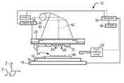
- Substrate 12 and substrate chuck 14may be further supported by stage 16 .
- Stage 16may provide motion along the x, y, and z axes.
- Stage 16 , substrate 12 , and substrate chuck 14may also be positioned on a base (not shown).
- Template 18 and/or mold 20may be formed from such materials including, but not limited to, fused-silica, quartz, silicon, organic polymers, siloxane polymers, borosilicate glass, fluorocarbon polymers, metal, hardened sapphire, and/or the like.
- patterning surface 22comprises features defined by a plurality of spaced-apart recesses 24 and/or protrusions 26 , though embodiments of the present invention are not limited to such configurations. Patterning surface 22 may define any original pattern that forms the basis of a pattern to be formed on substrate 12 .
- System 10may further comprise fluid dispense system 32 .
- Fluid dispense system 32may be used to deposit polymerizable material 34 on substrate 12 .
- Polymerizable material 34may be positioned upon substrate 12 using techniques such as drop dispense, spin-coating, dip coating, chemical vapor deposition (CVD), physical vapor deposition (PVD), thin film deposition, thick film deposition, and/or the like.
- Polymerizable material 34may be disposed upon substrate 12 before and/or after a desired volume is defined between mold 20 and substrate 12 depending on design considerations.
- Polymerizable material 34may comprise a monomer mixture as described in U.S. Pat. No. 7,157,036 and U.S. Patent Publication No. 2005/0187339, both of which are hereby incorporated by reference herein.
- system 10may further comprise energy source 38 coupled to direct energy 40 along path 42 .
- Imprint head 30 and stage 16may be configured to position template 18 and substrate 12 in superimposition with path 42 .
- System 10may be regulated by processor 54 in communication with stage 16 , imprint head 30 , fluid dispense system 32 , and/or source 38 , and may operate on a computer readable program stored in memory 56 .
- Either imprint head 30 , stage 16 , or bothvary a distance between mold 20 and substrate 12 to define a desired volume therebetween that is filled by polymerizable material 34 .
- imprint head 30may apply a force to template 18 such that mold 20 contacts polymerizable material 34 .
- source 38produces energy 40 , e.g., ultraviolet radiation, causing polymerizable material 34 to solidify and/or cross-link conforming to a shape of surface 44 of substrate 12 and patterning surface 22 , defining patterned layer 46 on substrate 12 .
- Patterned layer 46may comprise a residual layer 48 and a plurality of features shown as protrusions 50 and recessions 52 , with protrusions 50 having a thickness t 1 and residual layer having a thickness t 2 .
- treatment of template 18 with surfactant moleculesis provided as a diluted spray-on surfactant/solvent solution.
- the diluted spray-on surfactant/solvent solutionit is generally difficult to obtain precise distribution of the surfactant molecules on the templates.
- FIGS. 3A-3Cillustrate simplified side views of an exemplary embodiment for providing precise distribution of a surfactant on template 18 to provide two regions: a surfactant rich region SRR and a surfactant depleted region SDR.
- treatment of template 18by contacting template 18 with surfactant (e.g., surfactant liquid 60 ) deposited on substrate 12 , may provide control over distribution of surfactant liquid 60 to provide surfactant rich region SRR and surfactant depleted region SDR. Control of the distribution may further allow for control over the magnitude of the contact angle ⁇ SRR within the surfactant rich region SRR and the magnitude of the contact angle ⁇ SDR within the surfactant depleted region SDR.
- surfactante.g., surfactant liquid 60
- the contact angle ⁇ SRR within the surfactant rich region SRR and the contact angle ⁇ SDR within the surfactant depleted region SDRmay target different applications providing for ⁇ SRR > ⁇ SDR ; ⁇ SRR ⁇ SDR ; and/or ⁇ SRR ⁇ SRR ⁇ SDR .
- contact angles ⁇ SRR and/or ⁇ SDRmay be controlled to target different applications providing for ⁇ SRR > ⁇ SDR ; ⁇ SRR ⁇ SDR ; and/or ⁇ SRR ⁇ SDR .
- surface 62 of template 18initially may be substantially free of surfactant liquid 60 .
- surface 62 of template 18may be pre-treated.
- surface 62 of template 18may be pre-treated with the diluted spray-on surfactant/solvent solution described above.
- Imprint fluid 58may be deposited on substrate 12 .
- Imprint fluid 58may include, but is not limited to, polymerizable material 34 and surfactant liquid 60 .
- Polymerizable material 34may be formed from several different families of bulk materials.
- polymerizable material 34may be fabricated from bulk materials including, but not limited to, vinyl ethers, methacrylates, epoxies, thiol-enes and acrylates, and/or the like. Bulk materials are described in further detail in U.S. Pat. No. 7,307,118, which is hereby incorporated by reference herein.
- composition of surfactant liquid 60may provide for different contact angles; surfactant liquid 60 may be selected to provide an approximate contact angle ⁇ SRR at the surfactant rich regions SRR and an approximate contact angle ⁇ SDR at the surfactant depleted regions SDR. As such, selection of surfactant liquid 60 may provide ⁇ SRR > ⁇ SDR , ⁇ SRR ⁇ SDR , and/or ⁇ SRR ⁇ SDR , depending on the design considerations of an application.
- Exemplary surfactantmay include surfactant components such as fluoro-aliphatic polymeric esters, fluorosurfactants of polyoxyethylene, fluorosurfactants of polyalkyl ether, fluoroalkyl polyethers, and/or the like. Exemplary surfactant components are further described in U.S. Pat. No. 3,403,122, U.S. Pat. No. 3,787,351, U.S. Pat. No. 4,803,145, U.S. Pat. No. 4,835,084, U.S. Pat. No. 4,845,008, U.S. Pat. No. 5,380,644, U.S. Pat. No. 5,747,234, U.S. Pat. No. 6,664,354, and U.S. Patent Publication No. 2006/0175736, all of which are hereby incorporated by reference herein.
- surfactant componentssuch as fluoro-aliphatic polymeric esters, fluorosurfactants of polyoxyethylene, fluorosurfactants of polyalkyl
- Exemplary commercially available surfactant componentsinclude, but are not limited to, ZONYL® FSO, ZONYL® FSO-100, ZONYL® FSN-100, and ZONYL® FS-300, manufactured by E.I. du Pont de Nemours and Company having an office located in Wilmington, Del.; FC-4432, FC-4430, and FC-430, manufactured by 3M having an office located in Maplewood, Minn.; MASURF® FS425, MASURF® FS1700, MASURF® FS2000, MASURF® FS1239, manufactured by Mason Chemical Company having an office located in Arlington Heights, Ill.; Lodyne S-107B, Lodyne S-220N, manufactured by Ciba-Geigy Corporation having an office located in Basel, Switzerland; Unidyne NS1602, Unidyne NS1603, Unidyne NS1606a, manufactured by Daikin having an office located in Kita-ku, Osaka, Japan; MegaFace
- Selection of surfactantmay be provided through contact angle analysis.
- Contact angle analysismay include simulated testing of the contact angles on simulated surfactant rich regions SRR SIM and/or simulated surfactant depleted regions SDR SIM .
- testing substrate 72may be formed of material that is substantially similar to template 18 .
- testing substrate 72may be formed of fused silica.
- testing substrate 72may be sized such that it is substantially similar to template 18 and/or sized to accommodate at least one simulated surfactant rich region SRR SIM .
- Testing substrate 72may be cleaned, baked dry, and stored in a nitrogen box. As illustrated in FIG. 4A , testing substrate 72 may be rinsed with a surfactant solution to provide film 74 having a thickness t 5 .
- the surfactant solutionmay be a diluted surfactant solution.
- the surfactant solutionmay be a solution formed of a percentage of weight of surfactant molecules in Isopropyl Alcohol (IPA).
- IPAIsopropyl Alcohol
- Surfactant molecules within the surfactant solutionmay be similar to surfactant molecules within surfactant liquid 60 .
- Film 74 of the surfactant solution on testing substrate 72may be dried, and/or a substantial portion of film 74 may evaporate, reducing thickness t 5 as illustrated in FIG. 4B .
- thickness t 5may be substantially zero as IPA within the surfactant solution may be substantially evaporated.
- drops of imprint fluid 58may be deposited on testing substrate 72 to form the simulated surfactant rich region SRR SIM .
- Each drop of imprint fluid 58may have a volume V D .
- the volume V D of each dropmay be approximately 5 ⁇ L.
- the volume V Dmay include polymerizable material 34 and surfactant liquid 60 .
- Surfactant liquid 60may be comprised of similar surfactant molecules as compared to surfactant solution 74 .
- surfactant liquid 60may be comprised of different surfactant molecules as compared to surfactant solution 74 .
- the contact angle of imprint fluid 58 on testing substrate 72may be measured at multiple locations on testing substrate 72 .
- the contact angle of imprint fluid 58may be measured at several locations (e.g., seven locations) using goniometer 70 .
- the contact angles at multiple locationsmay be averaged to provide the magnitude of the contact angle ⁇ R-SIM on the simulated surfactant rich regions SRR SIM .
- testing substrate 72 a in FIG. 5Amay be cleaned, baked dry, and stored in a nitrogen box. Testing substrate 72 a may then be rinsed with a solvent (e.g., IPA) to provide film 78 having a thickness t 6 . Film 78 of solvent on testing substrate 72 a may be dried and/or at least a portion of film 78 of solvent may evaporate reducing thickness t 6 as illustrated in FIG. 5B . For example, thickness t 6 may be substantially zero after evaporation of a substantial portion of IPA.
- a solvente.g., IPA
- drops of imprint fluid 58may be deposited on testing substrate 72 a to form the simulated surfactant depleted region SDR SIM .
- Each drop of imprint fluid 58may have a volume V D2 .
- the volume V D2 of each dropmay be approximately 5 ⁇ L.
- the volume V D2may be substantially similar to the volume V D of drops on testing substrate 72 in FIG. 4 .
- the volume V D2 of drops on testing substrate 72 a in FIG. 5Cmay include polymerizable material 34 and surfactant liquid 60 .
- the contact angle of imprint fluid 58 on testing substrate 72 amay be measured at multiple locations on testing substrate 72 a .
- the contact angle of imprint fluid 58may be measured at several locations (e.g., seven locations) by goniometer 70 .
- the contact angles at multiple locationsmay be averaged to provide the magnitude of the contact angle ⁇ D-SIM on the simulated surfactant depleted regions SDR SIM .
- Variations of surfactant liquid 60 within imprint fluid 58 deposited on testing substrate 72 amay provide control over the contact angles within the simulated surfactant rich regions SRR SIM and/or the simulated surfactant depleted regions SDR SIM leading to control over the surfactant rich regions SRR and the surfactant depleted regions SDR during imprinting.
- imprint fluid 58 formed of surfactant liquid 60 having approximately 0.17% FC4432 and 0.33% FC4430 and polymerizable material 34may provide for ⁇ R-SIM of approximately 20° and ⁇ D-SIM of approximately 22° such that ⁇ R-SIM ⁇ D-SIM .
- imprint fluid 58 formed of surfactant liquid 60 having approximately 0.5% R-08 and polymerizable material 34may provide for ⁇ R-SIM of approximately 15° and ⁇ D-SIM of approximately 22° such that ⁇ R-SIM ⁇ D-SIM .
- imprint fluid 58 formed of surfactant liquid 60 having approximately 0.5% FS2000 and polymerizable material 34may provide for ⁇ R-SIM of approximately 18° and ⁇ D-SIM of approximately 10° such that ⁇ R-SIM > ⁇ D-SIM .
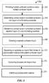
- FIG. 6illustrates a flow chart of exemplary method 300 for providing suitable wetting characteristics between template 18 and polymerizable material 34 .
- Suitable wetting characteristicsmay be created by controlling the contact angles ⁇ SRR and ⁇ SDR .
- surfactant liquid 60providing approximate the contact angles ⁇ R-SIM and ⁇ D-SIM may be selected such that ⁇ SRR > ⁇ SDR .
- Application of surfactant liquid 60 on template 18may then be controlled to provide the surfactant rich region SRR and the surfactant depleted region SDR on template 18 .
- the reduced contact angle ⁇ SDR in the surfactant depleted region SDR on template 18may provide polymerizable material 34 an additional driving force to wet the surfactant depleted region SDR.
- voids formed within patterned layer 46may be significantly reduced during imprinting.
- the contact angle ⁇ D-SIMmay be determined by a reference document (e.g., database) from prior testing using surfactant liquid 60 and solvent 78 .
- surfactant liquid 60 suitable for imprintingmay be determined.
- surfactant liquid 60 that provides ⁇ SRR > ⁇ SDRmay be selected.
- imprint material 58 formed of polymerizable material 34 and surfactant liquid 60may be deposited on substrate 12 . It should be noted that surfactant liquid 60 may be applied directly to template 18 and need not be directly added to polymerizable material 34 prior to contact of template 18 with polymerizable material 34 . Generally, surfactant liquid 60 in imprint fluid 58 may migrate towards the gas/liquid interface.
- template 18may contact imprint fluid 58 providing at least a portion of surfactant liquid 60 on surface 62 of template 18 to form at least one surfactant rich region SRR and at least one surfactant depleted region SDR.
- the approximate contact angle ⁇ SRR provided within at least one surfactant rich region SRR during imprintingmay be less than, greater than, or substantially similar to the approximate contact angle ⁇ SDR within at least one surfactant depleted region SDR during imprinting.
- polymerizable material 34may be solidified to provide patterned layer 46 .
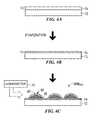
- distribution of surfactant on template 18may provide two regions: the surfactant rich region SRR and the surfactant depleted region SDR.
- the surfactant rich region SRR on template 18is generally located at the point of contact between template 18 and imprint fluid 58 .
- surfactant liquid 60 within imprint fluid 58may migrate to the gas/liquid interface as template 18 contacts imprint fluid 58 and imprint fluid 58 spreads on surface 44 of substrate 12 .
- surfactant liquid 60may build up in localized regions on template 18 forming surfactant depleted regions SDR at drop locations 80 and surfactant rich regions SRR between drop locations 80 .
- the surfactant rich regions SRR between drop locations 80generally form interstitial areas where voids may occur.
- Drop shiftingmay even out surfactant distribution on template 18 .
- FIG. 7Billustrates surfactant depleted regions SDR and surfactant rich regions SRR after a first drop pattern imprint.
- a second drop patternmay be used that provides drop locations 80 at a shifted location as compared to the first drop pattern.
- the shifted location of drops 80 in the subsequent drop patternmay be positioned such that at least one of drops 80 of imprint fluid 58 contacts template 18 at a surfactant rich region SRR.
- drop shift patterningmay be used successively or sporadically. For example, a first drop pattern may be used to imprint followed by one or more drop shifted patterns. Alternatively, a first drop pattern may be used multiple times prior to one or more drop shifted patterns being used. In a similar fashion, a first drop pattern may be used once followed by multiple uses of one or more drop shifted patterns.
- the lower contact angle ⁇ SDR of the surfactant depleted region SDRmay provide additional driving force for polymerizable material 34 to wet and fill the surfactant depleted region SDR.
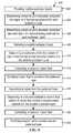
- FIG. 8illustrates a flow chart of another exemplary method 400 for providing suitable wetting characteristics between a template and a polymerizable material using drop pattern shifting.
- a step 402multiple surfactant solutions 74 and/or multiple surfactant liquids 60 may be provided.
- the contact angle ⁇ R-SIM in the simulated surfactant rich regions SRR SIM on testing substrate 72 rinsed with surfactant solution 74may be determined for each surfactant liquid 60 .
- the contact angle ⁇ D-SIM in the simulated surfactant depleted region SDR SIM on testing substrate 72 a rinsed in solvent 78may be determined for each surfactant liquid 60 .
- surfactant liquid 60 that provides a suitable contact anglemay be selected. For example, surfactant liquid 60 that provides contact angles ⁇ SRR > ⁇ SDR may be selected.
- imprint material 58 formed of polymerizable material 34 and surfactant liquid 60may be dispensed on substrate 12 in a first pattern. Generally, surfactant liquid 60 in imprint fluid 58 may migrate towards the gas/liquid interface.
- template 18may contact imprint fluid 58 .
- imprint fluid 58may be solidified to provide first patterned layer 46 .
- template 18may be separated from first patterned layer 46 with template 18 having the surfactant rich regions SRR and the surfactant depleted regions SDR upon removal.
- imprint material 58 formed of polymerizable material 34 and surfactant liquid 60may be dispensed in a second drop pattern on second substrate 12 .
- the second drop patternmay be substantially similar to the first drop pattern and shifted a position x and/or a position y such that at least one drop location contacts at least one surfactant depleted region SDR of template 18 .
- template 18may contact imprint fluid 58 .
- imprint fluid 58may be solidified to provide second patterned layer 46 .
- the second patterned layer 46may have limited or no voids.
Landscapes
- Engineering & Computer Science (AREA)
- Chemical & Material Sciences (AREA)
- Nanotechnology (AREA)
- Physics & Mathematics (AREA)
- General Physics & Mathematics (AREA)
- Crystallography & Structural Chemistry (AREA)
- Condensed Matter Physics & Semiconductors (AREA)
- Composite Materials (AREA)
- Manufacturing & Machinery (AREA)
- Materials Engineering (AREA)
- Mathematical Physics (AREA)
- Theoretical Computer Science (AREA)
- Shaping Of Tube Ends By Bending Or Straightening (AREA)
- Cleaning Or Drying Semiconductors (AREA)
- Moulds For Moulding Plastics Or The Like (AREA)
- Treatments Of Macromolecular Shaped Articles (AREA)
Abstract
Description
Claims (18)
Priority Applications (6)
| Application Number | Priority Date | Filing Date | Title |
|---|---|---|---|
| US12/336,821US8142703B2 (en) | 2005-10-05 | 2008-12-17 | Imprint lithography method |
| PCT/US2008/013827WO2009082458A2 (en) | 2007-12-18 | 2008-12-18 | Contact angle attenuations on multiple surfaces |
| JP2010539479AJP5020385B2 (en) | 2007-12-18 | 2008-12-18 | Reduction of contact angle on multiple surfaces |
| KR1020107015113AKR20100105659A (en) | 2007-12-18 | 2008-12-18 | Contact angle attenuations on multiple surfaces |
| CN2008801221593ACN101903159A (en) | 2007-12-18 | 2008-12-18 | Contact Angle Decay on Multiple Surfaces |
| EP08865713AEP2227575A4 (en) | 2007-12-18 | 2008-12-18 | Contact angle attenuations on multiple surfaces |
Applications Claiming Priority (3)
| Application Number | Priority Date | Filing Date | Title |
|---|---|---|---|
| US11/244,428US7837921B2 (en) | 2004-01-23 | 2005-10-05 | Method of providing desirable wetting and release characteristics between a mold and a polymerizable composition |
| US1457407P | 2007-12-18 | 2007-12-18 | |
| US12/336,821US8142703B2 (en) | 2005-10-05 | 2008-12-17 | Imprint lithography method |
Related Parent Applications (1)
| Application Number | Title | Priority Date | Filing Date |
|---|---|---|---|
| US11/244,428Continuation-In-PartUS7837921B2 (en) | 2003-06-17 | 2005-10-05 | Method of providing desirable wetting and release characteristics between a mold and a polymerizable composition |
Publications (2)
| Publication Number | Publication Date |
|---|---|
| US20090136654A1 US20090136654A1 (en) | 2009-05-28 |
| US8142703B2true US8142703B2 (en) | 2012-03-27 |
Family
ID=40801728
Family Applications (1)
| Application Number | Title | Priority Date | Filing Date |
|---|---|---|---|
| US12/336,821Active2026-05-09US8142703B2 (en) | 2005-10-05 | 2008-12-17 | Imprint lithography method |
Country Status (6)
| Country | Link |
|---|---|
| US (1) | US8142703B2 (en) |
| EP (1) | EP2227575A4 (en) |
| JP (1) | JP5020385B2 (en) |
| KR (1) | KR20100105659A (en) |
| CN (1) | CN101903159A (en) |
| WO (1) | WO2009082458A2 (en) |
Cited By (14)
| Publication number | Priority date | Publication date | Assignee | Title |
|---|---|---|---|---|
| US20100193994A1 (en)* | 2009-02-04 | 2010-08-05 | Asml Netherlands B.V. | Imprint lithography method and apparatus |
| US20130078817A1 (en)* | 2011-09-22 | 2013-03-28 | Tsukasa Azuma | Method of forming film, method of forming pattern, and method of manufacturing semiconductor device |
| US10208183B2 (en) | 2013-08-30 | 2019-02-19 | Canon Kabushiki Kaisha | Curable composition, film, and method of producing film |
| US10578965B2 (en) | 2016-03-31 | 2020-03-03 | Canon Kabushiki Kaisha | Pattern forming method |
| US10754243B2 (en) | 2016-03-31 | 2020-08-25 | Canon Kabushiki Kaisha | Pattern forming method as well as production methods for processed substrate, optical component, circuit board, electronic component and imprint mold |
| US10754245B2 (en) | 2016-03-31 | 2020-08-25 | Canon Kabushiki Kaisha | Pattern forming method as well as production methods for processed substrate, optical component, circuit board, electronic component and imprint mold |
| US10754244B2 (en) | 2016-03-31 | 2020-08-25 | Canon Kabushiki Kaisha | Pattern forming method as well as production methods for processed substrate, optical component, circuit board, electronic component and imprint mold |
| US10829644B2 (en) | 2016-03-31 | 2020-11-10 | Canon Kabushiki Kaisha | Pattern forming method as well as production methods for processed substrate, optical component, circuit board, electronic component and imprint mold |
| US10845700B2 (en) | 2016-03-31 | 2020-11-24 | Canon Kabushiki Kaisha | Pattern forming method as well as production methods for processed substrate, optical component, circuit board, electronic component and imprint mold |
| US10883006B2 (en) | 2016-03-31 | 2021-01-05 | Canon Kabushiki Kaisha | Pattern forming method as well as production methods for processed substrate, optical component, circuit board, electronic component and imprint mold |
| US10935884B2 (en) | 2017-03-08 | 2021-03-02 | Canon Kabushiki Kaisha | Pattern forming method and methods for manufacturing processed substrate, optical component and quartz mold replica as well as coating material for imprint pretreatment and set thereof with imprint resist |
| US11255715B2 (en) | 2018-07-20 | 2022-02-22 | Brighton technologies, LLC | Method and apparatus for determining a mass of a droplet from sample data collected from a liquid droplet dispensation system |
| US11281097B2 (en) | 2017-03-08 | 2022-03-22 | Canon Kabushiki Kaisha | Method for forming pattern by using photo-nanoimprint technology, imprint apparatus, and curable composition |
| US11327397B2 (en) | 2017-03-08 | 2022-05-10 | Canon Kabushiki Kaisha | Pattern forming method, coating material for imprint pretreatment and substrate pretreatment method |
Families Citing this family (13)
| Publication number | Priority date | Publication date | Assignee | Title |
|---|---|---|---|---|
| US7307118B2 (en)* | 2004-11-24 | 2007-12-11 | Molecular Imprints, Inc. | Composition to reduce adhesion between a conformable region and a mold |
| US20050160934A1 (en)* | 2004-01-23 | 2005-07-28 | Molecular Imprints, Inc. | Materials and methods for imprint lithography |
| US8808808B2 (en)* | 2005-07-22 | 2014-08-19 | Molecular Imprints, Inc. | Method for imprint lithography utilizing an adhesion primer layer |
| US8846195B2 (en)* | 2005-07-22 | 2014-09-30 | Canon Nanotechnologies, Inc. | Ultra-thin polymeric adhesion layer |
| US8142703B2 (en) | 2005-10-05 | 2012-03-27 | Molecular Imprints, Inc. | Imprint lithography method |
| US8272254B2 (en)* | 2008-08-04 | 2012-09-25 | Brighton Technologies Group, Inc | Device and method to measure wetting characteristics |
| US8361546B2 (en)* | 2008-10-30 | 2013-01-29 | Molecular Imprints, Inc. | Facilitating adhesion between substrate and patterned layer |
| US20100109195A1 (en) | 2008-11-05 | 2010-05-06 | Molecular Imprints, Inc. | Release agent partition control in imprint lithography |
| WO2011066450A2 (en)* | 2009-11-24 | 2011-06-03 | Molecular Imprints, Inc. | Adhesion layers in nanoimprint lithography |
| JP2011222732A (en) | 2010-04-09 | 2011-11-04 | Fujifilm Corp | Pattern formation method and patterned substrate manufacturing method |
| CN102507393B (en)* | 2011-11-08 | 2013-05-22 | 国网技术学院 | A coating surface contact angle measuring device and testing method |
| EP3210008B1 (en)* | 2014-10-24 | 2024-02-28 | Brighton Technologies LLC | Method and device for detecting substances on surfaces |
| JP7034696B2 (en)* | 2017-12-14 | 2022-03-14 | キヤノン株式会社 | A method for manufacturing a cured product pattern, a method for manufacturing a processed circuit board, a method for manufacturing a circuit board, a method for manufacturing electronic components, and a method for manufacturing an imprint mold. |
Citations (130)
| Publication number | Priority date | Publication date | Assignee | Title |
|---|---|---|---|---|
| US3403122A (en) | 1967-12-22 | 1968-09-24 | Minnesota Mining & Mfg | Emulsion polymerization of water insoluble omega-(n-perfluoroalkanesulfonyl) aminoalkyl acrylates or methacrylates |
| US3787351A (en) | 1972-02-28 | 1974-01-22 | Minnesota Mining & Mfg | Use of soluble fluoroaliphatic oligomers in resin composite articles |
| US3810874A (en) | 1969-03-10 | 1974-05-14 | Minnesota Mining & Mfg | Polymers prepared from poly(perfluoro-alkylene oxide) compounds |
| US4303761A (en) | 1979-05-29 | 1981-12-01 | E. I. Du Pont De Nemours And Company | Fluoroelastomer gelling agents and products made therefrom |
| US4512848A (en) | 1984-02-06 | 1985-04-23 | Exxon Research And Engineering Co. | Procedure for fabrication of microstructures over large areas using physical replication |
| US4585829A (en) | 1983-09-30 | 1986-04-29 | Union Carbide Corporation | Internal mold release for reaction injection molded polyurethanes |
| US4614667A (en) | 1984-05-21 | 1986-09-30 | Minnesota Mining And Manufacturing Company | Composite low surface energy liner of perfluoropolyether |
| US4617238A (en) | 1982-04-01 | 1986-10-14 | General Electric Company | Vinyloxy-functional organopolysiloxane compositions |
| US4731155A (en) | 1987-04-15 | 1988-03-15 | General Electric Company | Process for forming a lithographic mask |
| US4803145A (en) | 1986-03-28 | 1989-02-07 | Fuji Photo Film Co., Ltd. | Light sensitive alkali developable photoresist material with fluorine surfactant containing color layer |
| US4826943A (en) | 1986-07-25 | 1989-05-02 | Oki Electric Industry Co., Ltd. | Negative resist material |
| US4835084A (en) | 1988-03-21 | 1989-05-30 | Eastman Kodak Company | Electrostatographic toner and method of producing the same |
| US4845008A (en) | 1986-02-20 | 1989-07-04 | Fuji Photo Film Co., Ltd. | Light-sensitive positive working, o-guinone diazide presensitized plate with mixed solvent |
| US4931351A (en) | 1987-01-12 | 1990-06-05 | Eastman Kodak Company | Bilayer lithographic process |
| US5028366A (en) | 1988-01-12 | 1991-07-02 | Air Products And Chemicals, Inc. | Water based mold release compositions for making molded polyurethane foam |
| US5169494A (en) | 1989-03-27 | 1992-12-08 | Matsushita Electric Industrial Co., Ltd. | Fine pattern forming method |
| US5298556A (en) | 1992-07-21 | 1994-03-29 | Tse Industries, Inc. | Mold release composition and method coating a mold core |
| US5331020A (en) | 1991-11-14 | 1994-07-19 | Dow Corning Limited | Organosilicon compounds and compositions containing them |
| US5369722A (en) | 1991-09-18 | 1994-11-29 | Schott Glaswerke | Optical inorganic waveguide with a substantially planar organic substrate |
| US5380644A (en) | 1993-08-10 | 1995-01-10 | Minnesota Mining And Manufacturing Company | Additive for the reduction of mottle in photothermographic and thermographic elements |
| US5389696A (en) | 1993-09-17 | 1995-02-14 | Miles Inc. | Process for the production of molded products using internal mold release agents |
| US5397669A (en) | 1992-09-18 | 1995-03-14 | Minnesota Mining And Manufacturing Company | Liquid toners for use with perfluorinated solvents |
| US5425848A (en) | 1993-03-16 | 1995-06-20 | U.S. Philips Corporation | Method of providing a patterned relief of cured photoresist on a flat substrate surface and device for carrying out such a method |
| US5462700A (en) | 1993-11-08 | 1995-10-31 | Alliedsignal Inc. | Process for making an array of tapered photopolymerized waveguides |
| US5542978A (en) | 1994-06-10 | 1996-08-06 | Johnson & Johnson Vision Products, Inc. | Apparatus for applying a surfactant to mold surfaces |
| US5569691A (en) | 1993-03-05 | 1996-10-29 | Thera Patent Gmbh & Co. Kg Gesellschaft Fur Industrielle Schutzrechte | Hydrophilized polyethers |
| US5594042A (en) | 1993-05-18 | 1997-01-14 | Dow Corning Corporation | Radiation curable compositions containing vinyl ether functional polyorganosiloxanes |
| US5601641A (en) | 1992-07-21 | 1997-02-11 | Tse Industries, Inc. | Mold release composition with polybutadiene and method of coating a mold core |
| US5629095A (en) | 1993-05-18 | 1997-05-13 | Dow Corning Corporation | Radiation curable compositions containing vinyl ether functional polysiloxanes and methods for the preparation |
| US5629128A (en) | 1994-10-31 | 1997-05-13 | Fuji Photo Film Co., Ltd. | Positive photoresist composition |
| US5631314A (en) | 1994-04-27 | 1997-05-20 | Tokyo Ohka Kogyo Co., Ltd. | Liquid coating composition for use in forming photoresist coating films and photoresist material using said composition |
| US5747234A (en) | 1995-11-13 | 1998-05-05 | Eastman Kodak Company | Photographic element |
| US5772905A (en) | 1995-11-15 | 1998-06-30 | Regents Of The University Of Minnesota | Nanoimprint lithography |
| US5837314A (en) | 1994-06-10 | 1998-11-17 | Johnson & Johnson Vision Products, Inc. | Method and apparatus for applying a surfactant to mold surfaces |
| US5849222A (en) | 1995-09-29 | 1998-12-15 | Johnson & Johnson Vision Products, Inc. | Method for reducing lens hole defects in production of contact lens blanks |
| US5849209A (en) | 1995-03-31 | 1998-12-15 | Johnson & Johnson Vision Products, Inc. | Mold material made with additives |
| US5969063A (en) | 1997-07-11 | 1999-10-19 | Rohm And Haas Company | Preparation of fluorinated polymers |
| US6054034A (en) | 1990-02-28 | 2000-04-25 | Aclara Biosciences, Inc. | Acrylic microchannels and their use in electrophoretic applications |
| US6093455A (en) | 1997-05-23 | 2000-07-25 | Deco Patents, Inc. | Method and compositions for decorating glass |
| US6142811A (en) | 1999-04-09 | 2000-11-07 | Hon Hai Precision Ind. Co., Ltd. | Electrical connector |
| US6146811A (en) | 1998-08-01 | 2000-11-14 | Korea Advanced Institute Of Science And Technology | Photoresist using dioxaspiro ring-substituted acryl derivatives |
| US6169139B1 (en) | 1998-04-27 | 2001-01-02 | Dupont Dow Elastomers Llc | Fluoroelastomer latex |
| US6204343B1 (en) | 1996-12-11 | 2001-03-20 | 3M Innovative Properties Company | Room temperature curable resin |
| US6276273B1 (en) | 1999-06-11 | 2001-08-21 | Kodak Polychrome Graphics Llc | Surfactant-pretreated printing plate substrate, lithographic printing plate and method for production thereof |
| WO2000046035A9 (en) | 1999-02-04 | 2001-09-20 | Sun Chemical Corp | Printable media and method for its preparation by ink-jet printing |
| US6309580B1 (en) | 1995-11-15 | 2001-10-30 | Regents Of The University Of Minnesota | Release surfaces, particularly for use in nanoimprint lithography |
| US20010044075A1 (en) | 2000-04-25 | 2001-11-22 | Jsr Corporation | Radiation sensitive resin composition for forming barrier ribs for an EL display element, barrier rib and EL display element |
| US20010055727A1 (en) | 2000-05-12 | 2001-12-27 | Hiroshi Kubota | Resist material and method for pattern formation |
| US6334960B1 (en) | 1999-03-11 | 2002-01-01 | Board Of Regents, The University Of Texas System | Step and flash imprint lithography |
| US20020042027A1 (en) | 1998-10-09 | 2002-04-11 | Chou Stephen Y. | Microscale patterning and articles formed thereby |
| US6372838B1 (en) | 2000-06-28 | 2002-04-16 | 3M Innovative Properties Company | Fine latex and seed method of making |
| US6375870B1 (en) | 1998-11-17 | 2002-04-23 | Corning Incorporated | Replicating a nanoscale pattern |
| US6391217B2 (en) | 1999-12-23 | 2002-05-21 | University Of Massachusetts | Methods and apparatus for forming submicron patterns on films |
| US20020072009A1 (en) | 2000-12-13 | 2002-06-13 | Kim Hyun-Woo | Photosensitive polymer containing Si, Ge or Sn and resist composition comprising the same |
| US20020084553A1 (en) | 2000-12-13 | 2002-07-04 | Creavis Gesellschaft Fuer Techn. Und Innov. Mbh | Process for molding hydrophobic polymers to produce surfaces with stable water- and oil-repellent properties |
| US20020115002A1 (en) | 2000-10-12 | 2002-08-22 | Todd Bailey | Template for room temperature, low pressure micro-and nano-imprint lithography |
| WO2002069040A1 (en) | 2001-02-27 | 2002-09-06 | Shipley Company, Llc | Novel polymers, processes for polymer synthesis and photoresist compositions |
| US6447919B1 (en) | 1997-02-03 | 2002-09-10 | Cytonix Corporation | Hydrophobic coating compositions, articles coated with said compositions, and processes for manufacturing same |
| US20020126189A1 (en) | 2000-09-21 | 2002-09-12 | Gloster Daniel F. | Systems and methods for lithography |
| US20020132482A1 (en) | 2000-07-18 | 2002-09-19 | Chou Stephen Y. | Fluid pressure imprint lithography |
| US20020135099A1 (en) | 2001-01-19 | 2002-09-26 | Robinson Timothy R. | Mold with metal oxide surface compatible with ionic release agents |
| US20020146642A1 (en) | 2001-04-04 | 2002-10-10 | Kim Hyun-Woo | Photosensitive polymers and resist compositions comprising the photosensitive polymers |
| US6468642B1 (en) | 1995-10-03 | 2002-10-22 | N.V. Bekaert S.A. | Fluorine-doped diamond-like coatings |
| US6475704B1 (en) | 1997-09-12 | 2002-11-05 | Canon Kabushiki Kaisha | Method for forming fine structure |
| US6503914B1 (en) | 2000-10-23 | 2003-01-07 | Board Of Regents, The University Of Texas System | Thienopyrimidine-based inhibitors of the Src family |
| US6517995B1 (en) | 1999-09-14 | 2003-02-11 | Massachusetts Institute Of Technology | Fabrication of finely featured devices by liquid embossing |
| US6518189B1 (en) | 1995-11-15 | 2003-02-11 | Regents Of The University Of Minnesota | Method and apparatus for high density nanostructures |
| US6544594B2 (en) | 1999-09-10 | 2003-04-08 | Nano-Tex, Llc | Water-repellent and soil-resistant finish for textiles |
| US20030080472A1 (en) | 2001-10-29 | 2003-05-01 | Chou Stephen Y. | Lithographic method with bonded release layer for molding small patterns |
| US6565776B1 (en) | 1999-06-11 | 2003-05-20 | Bausch & Lomb Incorporated | Lens molds with protective coatings for production of contact lenses and other ophthalmic products |
| US6580172B2 (en) | 2001-03-02 | 2003-06-17 | Motorola, Inc. | Lithographic template and method of formation and use |
| WO2003073164A2 (en) | 2002-02-27 | 2003-09-04 | Brewer Science, Inc. | Novel planarization method for multi-layer lithography processing |
| US20030166814A1 (en) | 2002-02-28 | 2003-09-04 | David Sparrowe | Prepolymer material, polymer material, imprinting process and their use |
| EP1342736A2 (en) | 2002-02-28 | 2003-09-10 | MERCK PATENT GmbH | Prepolymer material, polymer material, imprinting process and their Use |
| US6646662B1 (en) | 1998-05-26 | 2003-11-11 | Seiko Epson Corporation | Patterning method, patterning apparatus, patterning template, and method for manufacturing the patterning template |
| US6649272B2 (en) | 2001-11-08 | 2003-11-18 | 3M Innovative Properties Company | Coating composition comprising fluorochemical polyether silane polycondensate and use thereof |
| US6664354B2 (en) | 1999-10-27 | 2003-12-16 | 3M Innovative Properties Company | Fluorochemical sulfonamide surfactants |
| US6664306B2 (en) | 2000-09-08 | 2003-12-16 | 3M Innovative Properties Company | Crosslinkable polymeric compositions and use thereof |
| US20030235787A1 (en) | 2002-06-24 | 2003-12-25 | Watts Michael P.C. | Low viscosity high resolution patterning material |
| US20040036201A1 (en) | 2000-07-18 | 2004-02-26 | Princeton University | Methods and apparatus of field-induced pressure imprint lithography |
| US20040046271A1 (en) | 2002-09-05 | 2004-03-11 | Watts Michael P.C. | Functional patterning material for imprint lithography processes |
| US20040046288A1 (en) | 2000-07-18 | 2004-03-11 | Chou Stephen Y. | Laset assisted direct imprint lithography |
| US20040065976A1 (en) | 2002-10-04 | 2004-04-08 | Sreenivasan Sidlgata V. | Method and a mold to arrange features on a substrate to replicate features having minimal dimensional variability |
| US20040065252A1 (en) | 2002-10-04 | 2004-04-08 | Sreenivasan Sidlgata V. | Method of forming a layer on a substrate to facilitate fabrication of metrology standards |
| US6721529B2 (en) | 2001-09-21 | 2004-04-13 | Nexpress Solutions Llc | Release agent donor member having fluorocarbon thermoplastic random copolymer overcoat |
| US6737489B2 (en) | 2001-05-21 | 2004-05-18 | 3M Innovative Properties Company | Polymers containing perfluorovinyl ethers and applications for such polymers |
| US20040110856A1 (en) | 2002-12-04 | 2004-06-10 | Young Jung Gun | Polymer solution for nanoimprint lithography to reduce imprint temperature and pressure |
| US20040116548A1 (en) | 2002-12-12 | 2004-06-17 | Molecular Imprints, Inc. | Compositions for dark-field polymerization and method of using the same for imprint lithography processes |
| US20040124566A1 (en) | 2002-07-11 | 2004-07-01 | Sreenivasan Sidlgata V. | Step and repeat imprint lithography processes |
| US20040131718A1 (en) | 2000-07-18 | 2004-07-08 | Princeton University | Lithographic apparatus for fluid pressure imprint lithography |
| US20040137734A1 (en) | 1995-11-15 | 2004-07-15 | Princeton University | Compositions and processes for nanoimprinting |
| WO2004061526A1 (en) | 2002-12-26 | 2004-07-22 | Nissan Chemical Industries, Ltd. | Alkali-soluble gap filling material forming composition for lithography |
| US6774183B1 (en) | 2000-04-27 | 2004-08-10 | Bostik, Inc. | Copolyesters having improved retained adhesion |
| US20040156108A1 (en) | 2001-10-29 | 2004-08-12 | Chou Stephen Y. | Articles comprising nanoscale patterns with reduced edge roughness and methods of making same |
| US6776094B1 (en) | 1993-10-04 | 2004-08-17 | President & Fellows Of Harvard College | Kit For Microcontact Printing |
| US20040168613A1 (en) | 2003-02-27 | 2004-09-02 | Molecular Imprints, Inc. | Composition and method to form a release layer |
| US20040170770A1 (en) | 2003-02-27 | 2004-09-02 | Molecular Imprints, Inc. | Method to reduce adhesion between a polymerizable layer and a substrate employing a fluorine-containing layer |
| US6790905B2 (en) | 2001-10-09 | 2004-09-14 | E. I. Du Pont De Nemours And Company | Highly repellent carpet protectants |
| US20040192041A1 (en) | 2003-03-27 | 2004-09-30 | Jun-Ho Jeong | UV nanoimprint lithography process using elementwise embossed stamp and selectively additive pressurization |
| US20040188381A1 (en) | 2003-03-25 | 2004-09-30 | Molecular Imprints, Inc. | Positive tone bi-layer imprint lithography method |
| US20040197843A1 (en) | 2001-07-25 | 2004-10-07 | Chou Stephen Y. | Nanochannel arrays and their preparation and use for high throughput macromolecular analysis |
| US6802870B2 (en) | 2001-05-25 | 2004-10-12 | 3M Innovative Properties Company | Method for imparting soil and stain resistance to carpet |
| US20040211754A1 (en) | 2003-04-25 | 2004-10-28 | Molecular Imprints, Inc. | Method of forming stepped structures employing imprint lithography |
| US6830819B2 (en) | 2003-03-18 | 2004-12-14 | Xerox Corporation | Fluorosilicone release agent for fluoroelastomer fuser members |
| US20040256764A1 (en)* | 2003-06-17 | 2004-12-23 | University Of Texas System Board Of Regents | Method to reduce adhesion between a conformable region and a pattern of a mold |
| EP1491356A2 (en) | 2003-06-25 | 2004-12-29 | Fuji Photo Film Co., Ltd. | Lithographic printing plate precursor and lithographic printing method |
| US6873087B1 (en) | 1999-10-29 | 2005-03-29 | Board Of Regents, The University Of Texas System | High precision orientation alignment and gap control stages for imprint lithography processes |
| US20050098534A1 (en) | 2003-11-12 | 2005-05-12 | Molecular Imprints, Inc. | Formation of conductive templates employing indium tin oxide |
| US20050160934A1 (en) | 2004-01-23 | 2005-07-28 | Molecular Imprints, Inc. | Materials and methods for imprint lithography |
| US6932934B2 (en) | 2002-07-11 | 2005-08-23 | Molecular Imprints, Inc. | Formation of discontinuous films during an imprint lithography process |
| US20050187339A1 (en) | 2004-02-23 | 2005-08-25 | Molecular Imprints, Inc. | Materials for imprint lithography |
| US20050192421A1 (en) | 2004-02-27 | 2005-09-01 | Molecular Imprints, Inc. | Composition for an etching mask comprising a silicon-containing material |
| US6957608B1 (en) | 2002-08-02 | 2005-10-25 | Kovio, Inc. | Contact print methods |
| US20060036051A1 (en) | 2004-08-16 | 2006-02-16 | Molecular Imprints, Inc. | Composition to provide a layer with uniform etch characteristics |
| US20060035029A1 (en) | 2004-08-16 | 2006-02-16 | Molecular Imprints, Inc. | Method to provide a layer with uniform etch characteristics |
| US20060062922A1 (en) | 2004-09-23 | 2006-03-23 | Molecular Imprints, Inc. | Polymerization technique to attenuate oxygen inhibition of solidification of liquids and composition therefor |
| US20060077374A1 (en) | 2002-07-11 | 2006-04-13 | Molecular Imprints, Inc. | Step and repeat imprint lithography systems |
| US20060081557A1 (en) | 2004-10-18 | 2006-04-20 | Molecular Imprints, Inc. | Low-k dielectric functional imprinting materials |
| US7037574B2 (en) | 2001-05-23 | 2006-05-02 | Veeco Instruments, Inc. | Atomic layer deposition for fabricating thin films |
| US20060108710A1 (en) | 2004-11-24 | 2006-05-25 | Molecular Imprints, Inc. | Method to reduce adhesion between a conformable region and a mold |
| US20060145398A1 (en) | 2004-12-30 | 2006-07-06 | Board Of Regents, The University Of Texas System | Release layer comprising diamond-like carbon (DLC) or doped DLC with tunable composition for imprint lithography templates and contact masks |
| US20070021520A1 (en) | 2005-07-22 | 2007-01-25 | Molecular Imprints, Inc. | Composition for adhering materials together |
| US20070017631A1 (en) | 2005-07-22 | 2007-01-25 | Molecular Imprints, Inc. | Method for adhering materials together |
| US20070212494A1 (en) | 2005-07-22 | 2007-09-13 | Molecular Imprints, Inc. | Method for Imprint Lithography Utilizing an Adhesion Primer Layer |
| US20070272825A1 (en) | 2004-01-23 | 2007-11-29 | Molecular Imprints, Inc. | Composition to Reduce Adhesion Between a Conformable Region and a Mold |
| US7309225B2 (en) | 2004-08-13 | 2007-12-18 | Molecular Imprints, Inc. | Moat system for an imprint lithography template |
| US20080000373A1 (en) | 2006-06-30 | 2008-01-03 | Maria Petrucci-Samija | Printing form precursor and process for preparing a stamp from the precursor |
| US20080110557A1 (en) | 2006-11-15 | 2008-05-15 | Molecular Imprints, Inc. | Methods and Compositions for Providing Preferential Adhesion and Release of Adjacent Surfaces |
| US20090136654A1 (en) | 2005-10-05 | 2009-05-28 | Molecular Imprints, Inc. | Contact Angle Attenuations on Multiple Surfaces |
| US20100109195A1 (en) | 2008-11-05 | 2010-05-06 | Molecular Imprints, Inc. | Release agent partition control in imprint lithography |
Family Cites Families (10)
| Publication number | Priority date | Publication date | Assignee | Title |
|---|---|---|---|---|
| JPH0224848A (en)* | 1988-07-14 | 1990-01-26 | Canon Inc | Production of substrate for optical recording medium |
| JPH0292603A (en)* | 1988-09-30 | 1990-04-03 | Hoya Corp | Manufacture of data recording board with guide groove |
| US6373489B1 (en)* | 1999-01-12 | 2002-04-16 | Schlumberger Technology Corporation | Scalable visualization for interactive geometry modeling |
| US7442336B2 (en)* | 2003-08-21 | 2008-10-28 | Molecular Imprints, Inc. | Capillary imprinting technique |
| KR100595515B1 (en)* | 2003-12-31 | 2006-07-03 | 엘지전자 주식회사 | Single layer film release agent coating method of mold for forming microstructure and mold for forming microstructure |
| CN1283445C (en)* | 2004-03-19 | 2006-11-08 | 中国科学院化学研究所 | Method for changing solid film material surface soakage |
| EP1838424B8 (en)* | 2004-11-24 | 2015-04-22 | Canon Nanotechnologies, Inc. | Method for reducing adhesion forces between an imprinting material and a mold, and use of an imprinting composition |
| JP4584754B2 (en)* | 2005-04-06 | 2010-11-24 | 株式会社日立産機システム | Nanoprint mold, method for producing the same, nanoprint apparatus using the mold, and nanoprint method |
| JP2007320142A (en)* | 2006-05-31 | 2007-12-13 | Meisho Kiko Kk | Mold for nanoimprinting |
| TWI340944B (en)* | 2006-10-27 | 2011-04-21 | Chimei Innolux Corp | Liquid crystal display, driving circuit and driving method thereof |
- 2008
- 2008-12-17USUS12/336,821patent/US8142703B2/enactiveActive
- 2008-12-18CNCN2008801221593Apatent/CN101903159A/enactivePending
- 2008-12-18WOPCT/US2008/013827patent/WO2009082458A2/enactiveApplication Filing
- 2008-12-18JPJP2010539479Apatent/JP5020385B2/enactiveActive
- 2008-12-18EPEP08865713Apatent/EP2227575A4/ennot_activeWithdrawn
- 2008-12-18KRKR1020107015113Apatent/KR20100105659A/ennot_activeWithdrawn
Patent Citations (156)
| Publication number | Priority date | Publication date | Assignee | Title |
|---|---|---|---|---|
| US3403122A (en) | 1967-12-22 | 1968-09-24 | Minnesota Mining & Mfg | Emulsion polymerization of water insoluble omega-(n-perfluoroalkanesulfonyl) aminoalkyl acrylates or methacrylates |
| US3810874A (en) | 1969-03-10 | 1974-05-14 | Minnesota Mining & Mfg | Polymers prepared from poly(perfluoro-alkylene oxide) compounds |
| US3787351A (en) | 1972-02-28 | 1974-01-22 | Minnesota Mining & Mfg | Use of soluble fluoroaliphatic oligomers in resin composite articles |
| US4303761A (en) | 1979-05-29 | 1981-12-01 | E. I. Du Pont De Nemours And Company | Fluoroelastomer gelling agents and products made therefrom |
| US4617238A (en) | 1982-04-01 | 1986-10-14 | General Electric Company | Vinyloxy-functional organopolysiloxane compositions |
| US4585829A (en) | 1983-09-30 | 1986-04-29 | Union Carbide Corporation | Internal mold release for reaction injection molded polyurethanes |
| US4512848A (en) | 1984-02-06 | 1985-04-23 | Exxon Research And Engineering Co. | Procedure for fabrication of microstructures over large areas using physical replication |
| US4614667A (en) | 1984-05-21 | 1986-09-30 | Minnesota Mining And Manufacturing Company | Composite low surface energy liner of perfluoropolyether |
| US4845008A (en) | 1986-02-20 | 1989-07-04 | Fuji Photo Film Co., Ltd. | Light-sensitive positive working, o-guinone diazide presensitized plate with mixed solvent |
| US4803145A (en) | 1986-03-28 | 1989-02-07 | Fuji Photo Film Co., Ltd. | Light sensitive alkali developable photoresist material with fluorine surfactant containing color layer |
| US4826943A (en) | 1986-07-25 | 1989-05-02 | Oki Electric Industry Co., Ltd. | Negative resist material |
| US4931351A (en) | 1987-01-12 | 1990-06-05 | Eastman Kodak Company | Bilayer lithographic process |
| US4731155A (en) | 1987-04-15 | 1988-03-15 | General Electric Company | Process for forming a lithographic mask |
| US5028366A (en) | 1988-01-12 | 1991-07-02 | Air Products And Chemicals, Inc. | Water based mold release compositions for making molded polyurethane foam |
| US4835084A (en) | 1988-03-21 | 1989-05-30 | Eastman Kodak Company | Electrostatographic toner and method of producing the same |
| US5169494A (en) | 1989-03-27 | 1992-12-08 | Matsushita Electric Industrial Co., Ltd. | Fine pattern forming method |
| US6054034A (en) | 1990-02-28 | 2000-04-25 | Aclara Biosciences, Inc. | Acrylic microchannels and their use in electrophoretic applications |
| US5369722A (en) | 1991-09-18 | 1994-11-29 | Schott Glaswerke | Optical inorganic waveguide with a substantially planar organic substrate |
| US5331020A (en) | 1991-11-14 | 1994-07-19 | Dow Corning Limited | Organosilicon compounds and compositions containing them |
| US5298556A (en) | 1992-07-21 | 1994-03-29 | Tse Industries, Inc. | Mold release composition and method coating a mold core |
| US5601641A (en) | 1992-07-21 | 1997-02-11 | Tse Industries, Inc. | Mold release composition with polybutadiene and method of coating a mold core |
| US5397669A (en) | 1992-09-18 | 1995-03-14 | Minnesota Mining And Manufacturing Company | Liquid toners for use with perfluorinated solvents |
| US5569691A (en) | 1993-03-05 | 1996-10-29 | Thera Patent Gmbh & Co. Kg Gesellschaft Fur Industrielle Schutzrechte | Hydrophilized polyethers |
| US5425848A (en) | 1993-03-16 | 1995-06-20 | U.S. Philips Corporation | Method of providing a patterned relief of cured photoresist on a flat substrate surface and device for carrying out such a method |
| US5861467A (en) | 1993-05-18 | 1999-01-19 | Dow Corning Corporation | Radiation curable siloxane compositions containing vinyl ether functionality and methods for their preparation |
| US5629095A (en) | 1993-05-18 | 1997-05-13 | Dow Corning Corporation | Radiation curable compositions containing vinyl ether functional polysiloxanes and methods for the preparation |
| US5594042A (en) | 1993-05-18 | 1997-01-14 | Dow Corning Corporation | Radiation curable compositions containing vinyl ether functional polyorganosiloxanes |
| US5380644A (en) | 1993-08-10 | 1995-01-10 | Minnesota Mining And Manufacturing Company | Additive for the reduction of mottle in photothermographic and thermographic elements |
| US5389696A (en) | 1993-09-17 | 1995-02-14 | Miles Inc. | Process for the production of molded products using internal mold release agents |
| US6776094B1 (en) | 1993-10-04 | 2004-08-17 | President & Fellows Of Harvard College | Kit For Microcontact Printing |
| US5462700A (en) | 1993-11-08 | 1995-10-31 | Alliedsignal Inc. | Process for making an array of tapered photopolymerized waveguides |
| US5631314A (en) | 1994-04-27 | 1997-05-20 | Tokyo Ohka Kogyo Co., Ltd. | Liquid coating composition for use in forming photoresist coating films and photoresist material using said composition |
| US5542978A (en) | 1994-06-10 | 1996-08-06 | Johnson & Johnson Vision Products, Inc. | Apparatus for applying a surfactant to mold surfaces |
| US5837314A (en) | 1994-06-10 | 1998-11-17 | Johnson & Johnson Vision Products, Inc. | Method and apparatus for applying a surfactant to mold surfaces |
| US5629128A (en) | 1994-10-31 | 1997-05-13 | Fuji Photo Film Co., Ltd. | Positive photoresist composition |
| US5849209A (en) | 1995-03-31 | 1998-12-15 | Johnson & Johnson Vision Products, Inc. | Mold material made with additives |
| US5849222A (en) | 1995-09-29 | 1998-12-15 | Johnson & Johnson Vision Products, Inc. | Method for reducing lens hole defects in production of contact lens blanks |
| US6468642B1 (en) | 1995-10-03 | 2002-10-22 | N.V. Bekaert S.A. | Fluorine-doped diamond-like coatings |
| US5747234A (en) | 1995-11-13 | 1998-05-05 | Eastman Kodak Company | Photographic element |
| US6809356B2 (en) | 1995-11-15 | 2004-10-26 | Regents Of The University Of Minnesota | Method and apparatus for high density nanostructures |
| US6518189B1 (en) | 1995-11-15 | 2003-02-11 | Regents Of The University Of Minnesota | Method and apparatus for high density nanostructures |
| US5772905A (en) | 1995-11-15 | 1998-06-30 | Regents Of The University Of Minnesota | Nanoimprint lithography |
| US6828244B2 (en) | 1995-11-15 | 2004-12-07 | Regents Of The University Of Minnesota | Method and apparatus for high density nanostructures |
| US20040137734A1 (en) | 1995-11-15 | 2004-07-15 | Princeton University | Compositions and processes for nanoimprinting |
| US6309580B1 (en) | 1995-11-15 | 2001-10-30 | Regents Of The University Of Minnesota | Release surfaces, particularly for use in nanoimprint lithography |
| US6204343B1 (en) | 1996-12-11 | 2001-03-20 | 3M Innovative Properties Company | Room temperature curable resin |
| US6447919B1 (en) | 1997-02-03 | 2002-09-10 | Cytonix Corporation | Hydrophobic coating compositions, articles coated with said compositions, and processes for manufacturing same |
| US6093455A (en) | 1997-05-23 | 2000-07-25 | Deco Patents, Inc. | Method and compositions for decorating glass |
| US5969063A (en) | 1997-07-11 | 1999-10-19 | Rohm And Haas Company | Preparation of fluorinated polymers |
| US6475704B1 (en) | 1997-09-12 | 2002-11-05 | Canon Kabushiki Kaisha | Method for forming fine structure |
| US6169139B1 (en) | 1998-04-27 | 2001-01-02 | Dupont Dow Elastomers Llc | Fluoroelastomer latex |
| US6646662B1 (en) | 1998-05-26 | 2003-11-11 | Seiko Epson Corporation | Patterning method, patterning apparatus, patterning template, and method for manufacturing the patterning template |
| US20020167117A1 (en) | 1998-06-30 | 2002-11-14 | Regents Of The University Of Minnesota | Release surfaces, particularly for use in nanoimprint lithography |
| US20030034329A1 (en) | 1998-06-30 | 2003-02-20 | Chou Stephen Y. | Lithographic method for molding pattern with nanoscale depth |
| US6146811A (en) | 1998-08-01 | 2000-11-14 | Korea Advanced Institute Of Science And Technology | Photoresist using dioxaspiro ring-substituted acryl derivatives |
| US6713238B1 (en) | 1998-10-09 | 2004-03-30 | Stephen Y. Chou | Microscale patterning and articles formed thereby |
| US20020042027A1 (en) | 1998-10-09 | 2002-04-11 | Chou Stephen Y. | Microscale patterning and articles formed thereby |
| US20040118809A1 (en) | 1998-10-09 | 2004-06-24 | Chou Stephen Y. | Microscale patterning and articles formed thereby |
| US6375870B1 (en) | 1998-11-17 | 2002-04-23 | Corning Incorporated | Replicating a nanoscale pattern |
| WO2000046035A9 (en) | 1999-02-04 | 2001-09-20 | Sun Chemical Corp | Printable media and method for its preparation by ink-jet printing |
| US6334960B1 (en) | 1999-03-11 | 2002-01-01 | Board Of Regents, The University Of Texas System | Step and flash imprint lithography |
| US20050236739A1 (en) | 1999-03-11 | 2005-10-27 | Board Of Regents, The University Of Texas System | Step and flash imprint lithography |
| US6719915B2 (en) | 1999-03-11 | 2004-04-13 | Board Of Regents, The University Of Texas System | Step and flash imprint lithography |
| WO2000054107A9 (en) | 1999-03-11 | 2002-05-02 | Univ Texas | Step and flash imprint lithography |
| US6142811A (en) | 1999-04-09 | 2000-11-07 | Hon Hai Precision Ind. Co., Ltd. | Electrical connector |
| US6565776B1 (en) | 1999-06-11 | 2003-05-20 | Bausch & Lomb Incorporated | Lens molds with protective coatings for production of contact lenses and other ophthalmic products |
| US6276273B1 (en) | 1999-06-11 | 2001-08-21 | Kodak Polychrome Graphics Llc | Surfactant-pretreated printing plate substrate, lithographic printing plate and method for production thereof |
| US6544594B2 (en) | 1999-09-10 | 2003-04-08 | Nano-Tex, Llc | Water-repellent and soil-resistant finish for textiles |
| US6517995B1 (en) | 1999-09-14 | 2003-02-11 | Massachusetts Institute Of Technology | Fabrication of finely featured devices by liquid embossing |
| US6664354B2 (en) | 1999-10-27 | 2003-12-16 | 3M Innovative Properties Company | Fluorochemical sulfonamide surfactants |
| US6873087B1 (en) | 1999-10-29 | 2005-03-29 | Board Of Regents, The University Of Texas System | High precision orientation alignment and gap control stages for imprint lithography processes |
| US6391217B2 (en) | 1999-12-23 | 2002-05-21 | University Of Massachusetts | Methods and apparatus for forming submicron patterns on films |
| US20010044075A1 (en) | 2000-04-25 | 2001-11-22 | Jsr Corporation | Radiation sensitive resin composition for forming barrier ribs for an EL display element, barrier rib and EL display element |
| US6774183B1 (en) | 2000-04-27 | 2004-08-10 | Bostik, Inc. | Copolyesters having improved retained adhesion |
| US20010055727A1 (en) | 2000-05-12 | 2001-12-27 | Hiroshi Kubota | Resist material and method for pattern formation |
| US6372838B1 (en) | 2000-06-28 | 2002-04-16 | 3M Innovative Properties Company | Fine latex and seed method of making |
| US6482742B1 (en) | 2000-07-18 | 2002-11-19 | Stephen Y. Chou | Fluid pressure imprint lithography |
| US20020132482A1 (en) | 2000-07-18 | 2002-09-19 | Chou Stephen Y. | Fluid pressure imprint lithography |
| US20040131718A1 (en) | 2000-07-18 | 2004-07-08 | Princeton University | Lithographic apparatus for fluid pressure imprint lithography |
| US20040046288A1 (en) | 2000-07-18 | 2004-03-11 | Chou Stephen Y. | Laset assisted direct imprint lithography |
| US20040036201A1 (en) | 2000-07-18 | 2004-02-26 | Princeton University | Methods and apparatus of field-induced pressure imprint lithography |
| US6664306B2 (en) | 2000-09-08 | 2003-12-16 | 3M Innovative Properties Company | Crosslinkable polymeric compositions and use thereof |
| US20020126189A1 (en) | 2000-09-21 | 2002-09-12 | Gloster Daniel F. | Systems and methods for lithography |
| US20020115002A1 (en) | 2000-10-12 | 2002-08-22 | Todd Bailey | Template for room temperature, low pressure micro-and nano-imprint lithography |
| US6696220B2 (en) | 2000-10-12 | 2004-02-24 | Board Of Regents, The University Of Texas System | Template for room temperature, low pressure micro-and nano-imprint lithography |
| US6503914B1 (en) | 2000-10-23 | 2003-01-07 | Board Of Regents, The University Of Texas System | Thienopyrimidine-based inhibitors of the Src family |
| US20020072009A1 (en) | 2000-12-13 | 2002-06-13 | Kim Hyun-Woo | Photosensitive polymer containing Si, Ge or Sn and resist composition comprising the same |
| US20020084553A1 (en) | 2000-12-13 | 2002-07-04 | Creavis Gesellschaft Fuer Techn. Und Innov. Mbh | Process for molding hydrophobic polymers to produce surfaces with stable water- and oil-repellent properties |
| US20020135099A1 (en) | 2001-01-19 | 2002-09-26 | Robinson Timothy R. | Mold with metal oxide surface compatible with ionic release agents |
| WO2002069040A1 (en) | 2001-02-27 | 2002-09-06 | Shipley Company, Llc | Novel polymers, processes for polymer synthesis and photoresist compositions |
| US6580172B2 (en) | 2001-03-02 | 2003-06-17 | Motorola, Inc. | Lithographic template and method of formation and use |
| US20020146642A1 (en) | 2001-04-04 | 2002-10-10 | Kim Hyun-Woo | Photosensitive polymers and resist compositions comprising the photosensitive polymers |
| US6737489B2 (en) | 2001-05-21 | 2004-05-18 | 3M Innovative Properties Company | Polymers containing perfluorovinyl ethers and applications for such polymers |
| US7037574B2 (en) | 2001-05-23 | 2006-05-02 | Veeco Instruments, Inc. | Atomic layer deposition for fabricating thin films |
| US6802870B2 (en) | 2001-05-25 | 2004-10-12 | 3M Innovative Properties Company | Method for imparting soil and stain resistance to carpet |
| US20040197843A1 (en) | 2001-07-25 | 2004-10-07 | Chou Stephen Y. | Nanochannel arrays and their preparation and use for high throughput macromolecular analysis |
| US6721529B2 (en) | 2001-09-21 | 2004-04-13 | Nexpress Solutions Llc | Release agent donor member having fluorocarbon thermoplastic random copolymer overcoat |
| US6790905B2 (en) | 2001-10-09 | 2004-09-14 | E. I. Du Pont De Nemours And Company | Highly repellent carpet protectants |
| US20030080471A1 (en) | 2001-10-29 | 2003-05-01 | Chou Stephen Y. | Lithographic method for molding pattern with nanoscale features |
| US20030080472A1 (en) | 2001-10-29 | 2003-05-01 | Chou Stephen Y. | Lithographic method with bonded release layer for molding small patterns |
| US20040156108A1 (en) | 2001-10-29 | 2004-08-12 | Chou Stephen Y. | Articles comprising nanoscale patterns with reduced edge roughness and methods of making same |
| US6649272B2 (en) | 2001-11-08 | 2003-11-18 | 3M Innovative Properties Company | Coating composition comprising fluorochemical polyether silane polycondensate and use thereof |
| WO2003073164A2 (en) | 2002-02-27 | 2003-09-04 | Brewer Science, Inc. | Novel planarization method for multi-layer lithography processing |
| US20030166814A1 (en) | 2002-02-28 | 2003-09-04 | David Sparrowe | Prepolymer material, polymer material, imprinting process and their use |
| EP1342736A2 (en) | 2002-02-28 | 2003-09-10 | MERCK PATENT GmbH | Prepolymer material, polymer material, imprinting process and their Use |
| US20030235787A1 (en) | 2002-06-24 | 2003-12-25 | Watts Michael P.C. | Low viscosity high resolution patterning material |
| US6932934B2 (en) | 2002-07-11 | 2005-08-23 | Molecular Imprints, Inc. | Formation of discontinuous films during an imprint lithography process |
| US20060077374A1 (en) | 2002-07-11 | 2006-04-13 | Molecular Imprints, Inc. | Step and repeat imprint lithography systems |
| US20040124566A1 (en) | 2002-07-11 | 2004-07-01 | Sreenivasan Sidlgata V. | Step and repeat imprint lithography processes |
| US20060076717A1 (en) | 2002-07-11 | 2006-04-13 | Molecular Imprints, Inc. | Step and repeat imprint lithography processes |
| US20060062867A1 (en) | 2002-07-11 | 2006-03-23 | Molecular Imprints, Inc. | Formation of discontinuous films during an imprint lithography process |
| US6957608B1 (en) | 2002-08-02 | 2005-10-25 | Kovio, Inc. | Contact print methods |
| US6936194B2 (en) | 2002-09-05 | 2005-08-30 | Molecular Imprints, Inc. | Functional patterning material for imprint lithography processes |
| US20040046271A1 (en) | 2002-09-05 | 2004-03-11 | Watts Michael P.C. | Functional patterning material for imprint lithography processes |
| US20040065252A1 (en) | 2002-10-04 | 2004-04-08 | Sreenivasan Sidlgata V. | Method of forming a layer on a substrate to facilitate fabrication of metrology standards |
| US20040065976A1 (en) | 2002-10-04 | 2004-04-08 | Sreenivasan Sidlgata V. | Method and a mold to arrange features on a substrate to replicate features having minimal dimensional variability |
| US20040110856A1 (en) | 2002-12-04 | 2004-06-10 | Young Jung Gun | Polymer solution for nanoimprint lithography to reduce imprint temperature and pressure |
| US7365103B2 (en) | 2002-12-12 | 2008-04-29 | Board Of Regents, The University Of Texas System | Compositions for dark-field polymerization and method of using the same for imprint lithography processes |
| US20040116548A1 (en) | 2002-12-12 | 2004-06-17 | Molecular Imprints, Inc. | Compositions for dark-field polymerization and method of using the same for imprint lithography processes |
| WO2004061526A1 (en) | 2002-12-26 | 2004-07-22 | Nissan Chemical Industries, Ltd. | Alkali-soluble gap filling material forming composition for lithography |
| US20040168613A1 (en) | 2003-02-27 | 2004-09-02 | Molecular Imprints, Inc. | Composition and method to form a release layer |
| US20040170770A1 (en) | 2003-02-27 | 2004-09-02 | Molecular Imprints, Inc. | Method to reduce adhesion between a polymerizable layer and a substrate employing a fluorine-containing layer |
| US6830819B2 (en) | 2003-03-18 | 2004-12-14 | Xerox Corporation | Fluorosilicone release agent for fluoroelastomer fuser members |
| US20040188381A1 (en) | 2003-03-25 | 2004-09-30 | Molecular Imprints, Inc. | Positive tone bi-layer imprint lithography method |
| US20040192041A1 (en) | 2003-03-27 | 2004-09-30 | Jun-Ho Jeong | UV nanoimprint lithography process using elementwise embossed stamp and selectively additive pressurization |
| US20040211754A1 (en) | 2003-04-25 | 2004-10-28 | Molecular Imprints, Inc. | Method of forming stepped structures employing imprint lithography |
| US20060279024A1 (en) | 2003-06-17 | 2006-12-14 | Molecular Imprints, Inc. | Method for providing desirable wetting and release characteristics between a mold and a polymerizable composition |
| WO2005000552A3 (en) | 2003-06-17 | 2005-06-30 | Molecular Imprints Inc | Method to reduce adhesion between a conformable region and a pattern of a mold |
| US7157036B2 (en) | 2003-06-17 | 2007-01-02 | Molecular Imprints, Inc | Method to reduce adhesion between a conformable region and a pattern of a mold |
| US20040256764A1 (en)* | 2003-06-17 | 2004-12-23 | University Of Texas System Board Of Regents | Method to reduce adhesion between a conformable region and a pattern of a mold |
| US20090272875A1 (en) | 2003-06-17 | 2009-11-05 | Molecular Imprints, Inc. | Composition to Reduce Adhesion Between a Conformable Region and a Mold |
| EP1491356A2 (en) | 2003-06-25 | 2004-12-29 | Fuji Photo Film Co., Ltd. | Lithographic printing plate precursor and lithographic printing method |
| US20050098534A1 (en) | 2003-11-12 | 2005-05-12 | Molecular Imprints, Inc. | Formation of conductive templates employing indium tin oxide |
| WO2005072120A2 (en) | 2004-01-23 | 2005-08-11 | Molecular Imprints, Inc. | Materials and methods for imprint lithography |
| US7837921B2 (en) | 2004-01-23 | 2010-11-23 | Molecular Imprints, Inc. | Method of providing desirable wetting and release characteristics between a mold and a polymerizable composition |
| US20070272825A1 (en) | 2004-01-23 | 2007-11-29 | Molecular Imprints, Inc. | Composition to Reduce Adhesion Between a Conformable Region and a Mold |
| US20050160934A1 (en) | 2004-01-23 | 2005-07-28 | Molecular Imprints, Inc. | Materials and methods for imprint lithography |
| WO2005082992A1 (en) | 2004-02-23 | 2005-09-09 | Molecular Imprints, Inc. | Materials for imprint lithography |
| US20050187339A1 (en) | 2004-02-23 | 2005-08-25 | Molecular Imprints, Inc. | Materials for imprint lithography |
| US20050192421A1 (en) | 2004-02-27 | 2005-09-01 | Molecular Imprints, Inc. | Composition for an etching mask comprising a silicon-containing material |
| US7309225B2 (en) | 2004-08-13 | 2007-12-18 | Molecular Imprints, Inc. | Moat system for an imprint lithography template |
| US20060036051A1 (en) | 2004-08-16 | 2006-02-16 | Molecular Imprints, Inc. | Composition to provide a layer with uniform etch characteristics |
| US20060035029A1 (en) | 2004-08-16 | 2006-02-16 | Molecular Imprints, Inc. | Method to provide a layer with uniform etch characteristics |
| US20070141271A1 (en) | 2004-09-23 | 2007-06-21 | Molecular Imprints, Inc. | Method for controlling distribution of fluid components on a body |
| US20060062922A1 (en) | 2004-09-23 | 2006-03-23 | Molecular Imprints, Inc. | Polymerization technique to attenuate oxygen inhibition of solidification of liquids and composition therefor |
| US20060081557A1 (en) | 2004-10-18 | 2006-04-20 | Molecular Imprints, Inc. | Low-k dielectric functional imprinting materials |
| US7307118B2 (en) | 2004-11-24 | 2007-12-11 | Molecular Imprints, Inc. | Composition to reduce adhesion between a conformable region and a mold |
| US20060108710A1 (en) | 2004-11-24 | 2006-05-25 | Molecular Imprints, Inc. | Method to reduce adhesion between a conformable region and a mold |
| US20060145398A1 (en) | 2004-12-30 | 2006-07-06 | Board Of Regents, The University Of Texas System | Release layer comprising diamond-like carbon (DLC) or doped DLC with tunable composition for imprint lithography templates and contact masks |
| US20070212494A1 (en) | 2005-07-22 | 2007-09-13 | Molecular Imprints, Inc. | Method for Imprint Lithography Utilizing an Adhesion Primer Layer |
| US20070021520A1 (en) | 2005-07-22 | 2007-01-25 | Molecular Imprints, Inc. | Composition for adhering materials together |
| US20070017631A1 (en) | 2005-07-22 | 2007-01-25 | Molecular Imprints, Inc. | Method for adhering materials together |
| US20090136654A1 (en) | 2005-10-05 | 2009-05-28 | Molecular Imprints, Inc. | Contact Angle Attenuations on Multiple Surfaces |
| US20080000373A1 (en) | 2006-06-30 | 2008-01-03 | Maria Petrucci-Samija | Printing form precursor and process for preparing a stamp from the precursor |
| US20080110557A1 (en) | 2006-11-15 | 2008-05-15 | Molecular Imprints, Inc. | Methods and Compositions for Providing Preferential Adhesion and Release of Adjacent Surfaces |
| US20100109195A1 (en) | 2008-11-05 | 2010-05-06 | Molecular Imprints, Inc. | Release agent partition control in imprint lithography |
Non-Patent Citations (58)
| Title |
|---|
| 3M Novec Fluorosurfactant FC-4432, Product Information, www.3m.com/paintsandcoatings, Oct. 2003, 4 pages (MII 05-353). |
| Bailey et al., Step and Flash Imprint Lithography: Defect Analysis, Journal of Vacuum Science, B 19(6), pp. 2806-2810 Nov. 1, 2001. |
| Bailey et al., Step and Flash Imprint Lithography: Template Surface Treatment and Defect Analysis, Journal of Vacuum Science, B 18(6), pp. 3572-3577 Nov. 1, 2000. |
| Bender et al., Multiple imprinting in UV-based nanoimprint lithography: related material issues, Microelectronic Engineering 53 (2000), pp. 233-236. |
| Bender et al., Multiple Imprinting in UV-based Nanoimprint Lithography: Related Material Issues, Microelectronic Engineering 61-62, pp. 407-413 Jan. 1, 2002. |
| Bongiovanni et al., "High resolution XPS investigation of photocured films containing perfluoropolyether acrylates", Polymer, Elsevier Science Publishers B.V, GB, vol. 41, No. 2, Jan. 1, 2000, pp. 409-414. |
| Butter et al., Production and Wetting Properties of Fluorinated Diamond-Like Carbon Coatings, Thin Solid Films, 311(1-2); pp. 107-113 Dec. 31, 1997. |
| Choi et al., Design of Orientation Stages for Step and Flash Imprint Lithography, Precision Engineering, pp. 192-199 Jan. 1, 2001. |
| Chou et al., Imprint Lithography with 25-Nanometer Resolution, Science vol. 272, pp. 85-87 Apr. 5, 1996. |
| Chou et al., Imprint Lithography with Sub-10 nm Feature Size and High Throughput, Microelectronic Engineering 35, pp. 237-240 Jan. 1, 1997. |
| Chou et al., Imprint of Sub-25 nm Vias and Trenches in Polymers, Appl. Phys. Lett. 67 (21) Nov. 20, 1995. |
| Chou et al., Lithographically Induced Self-assembly of Periodic Polymer Micropillar Arrays, J. Vac. Sci. Technol. B 17 (6), pp. 3197-3202 Nov. 1, 1999. |
| Chou et al., Nanoimprint Lithography, Journal of Vacuum Science Technolgoy B 14(16), pp. 4129-4133 Nov. 1, 1996. |
| Chou et al., Ultrafast and Direct Imprint of Nanostructures in Silicon, Nature, Col. 417, (Jun. 2002), pp. 835-837 Jun. 1, 2002. |
| Chou, Nanoimprint Lithography and Lithographically Induced Self-Assembly, MRS Bulletin, pp. 512-517 Jul. 1, 2001. |
| Colburn et al., Characterization and Modeling of Volumetric and Mechanical Properties for Step and Flash Imprint Lithography Photopolyrners, Journal of Vacuum Science Technology. vol b. 19(6) Nov. 1, 2001. |
| Colburn et al., Development and Advantages of Step-and-Flash Lithography, Solid State Technology Jul. 1, 2001. |
| Colburn et al., Step and Flash Imprint Lithography for sub-100 nm Patterning, Proceedings of SPIE vol. 3997, pp. 453-457 Jan. 1, 2000. |
| Colburn et al., Step and Flash Imprint Lithography: A New Approach to High-Resolution Patterning, Proc. of SPIE, vol. 3676 Mar. 1, 1999. |
| Colburn, Dissertation for the Degree of Doctor of Philosophy, Step and Flash Imprint Lithography: A Low-Pressure, Room-Temperature Nanoimprint Lithography Aug. 1, 2001. |
| Compon et al., Electroanalysis at Diamond-Like and Doped-Diamond Electrodes, Electroanalysis 15(17); pp. 1349-1363 Sep. 1, 2003. |
| DuPont Zonyl Fluorochemical Intermediates, www.dupont.com/zonyl/pdf/intermediates.pdf; pp. 1-16 Jun. 21, 2003. |
| DuPont Zonyl FSN, www.dupont.com/zonyl/odf/FSN.pdf; pp. 1-2 Aug. 24, 2003. |
| DuPont Zonyl UR, www.dupont.com/zonyl/pdf/UR.pdf; pp. 1-2 Jun. 21, 2003. |
| European Search Report for Application No. EP05820878, dated Oct. 28, 2010, 7 pages. |
| European Search Report for Application No. EP10181754, dated Oct. 26, 2010, 6 pages. |
| FC-4432 Produce Brochure, 3M Fluorosurfactant Mar. 1, 2002. |
| Fukuhara et al., UV Nanoimprint Lithography and Its Application for Nanodevices, Journal of Photopolymer Science and Technology 20:4 (2007) pp. 549-554. |
| Guo et al., Nanoimprint Lithogrpahy: Methods and Material Requirements, Advanced Materials 19 (2007) pp. 495-513. |
| Haisma et al., Mold-assisted Nanolithography: A Process for Reliable Pattern Replication, J. Vac. Sci. Technol. B, pp. 4124-4128 Nov. 1, 1996. |
| Hakovirta et al., Heat Resistance of Fluorinated Diamond-Like Carbon Films, Diamond and Related Materiasl 10(8); pp. 1486-1490 Aug. 1, 2001. |
| Heidari, Nanoimprint Lithography at the 6 in. Wafer Scale, J. Vac. Sci. Technol. B 18(6), pp. 3557-3560 Nov. 1, 2000. |
| Hirai et al., Mold Surface Treatment for Imprint Lithography, Journal of Photopolymer Science and Technology, vol. 14, No. 3, pp. 457-462 Aug. 1, 2001. |
| International Search Report for Application No. PCT/US05/04415, dated Jun. 15, 2005, 1 page. |
| International Search Report for Application No. PCT/US2004/18857, dated Apr. 26, 2005, 2 pages. |
| International Search Report for Application No. PCT/US2005/001054, dated Aug. 29, 2005, 1 page. |
| International Search Report for Application No. PCT/US2008/013827, dated Apr. 7, 2009, 1 page. |
| International Search Report for Application No. PCT/US2009/005990, dated Sep. 15, 2010, 11 pages. |
| Johnson et al., Advances in Step and Flash Imprint Lithography, SPIE Microlithography Conference Feb. 23, 2003. |
| Jung et al., Orientation-Controlled Self-Assembled Nanolithography Using a Polystyrene-Polydimethylsiloxane Block Copolymer, Nano Letters, vol. 7, No. 7, pp. 2046-2050 (2007) Apr. 19, 2007. |
| Kim et al., Fabrication of Trilayer Resist Using Photocuring-Imprint Lithography, Journal of Vacuum Science and Technology B 21:6 (2003) pp. 3144-3148. |
| Komuro et al., Improvement of Imprinted Pattern Uniformity Using Sapphire Mold, Japanese Journal Applied Physics 41 (2002) 4182-4185. |
| Lin et al., Role of surfactants in adhesion reduction for step and flash imprint lithography, J. Micro/Nanolith., MEMS MOEMS 7(3) Jul.-Sep. 2008, 8 pages. |
| Mansano et al., Protective Carbon Layer for Chemical Corrosion of Stainless Steel, Diamond and Related Materials 12 (3-7); pp. 749-752 Mar. 1, 2003. |
| Masurf FS-230, www.masonsurfactants.com/Products/Masurf-FS-230.htm; pp. 1-2 Apr. 5, 2004. |
| Roos et al., Nanoimprint Lithography with a Commercial 4 Inch Bond System for Hot embossing, Proceedings of SPIE vol. 4343, pp. 427-435 Oct. 1, 2001. |
| Scheerlinck et al., Nano Imprint Lithography for Photonic Structure Patterning, Proceedings Symposium IEEE/LEOS. Benelux Chapter, 2005, Mons, pp. 63-66. |
| Schneider et al., Stripes of Partially Fluorinated Alkyl Chains: Dipolar Langmuir Monolayers, J. Chem. Phys. vol. 122, Issue 9 Mar. 1, 2005. |
| Taniguchi et al., Measurement of Adhesive Force Between Mold and Photocurable Resin in Imprint Technology, Japanese Journal of Applied Physics 41(2002) 4194-4197. |
| Translation of Japanese Patent 02-24848, Jan. 26, 1990. |
| Translation of Japanese Patent 02-92603, Apr. 3, 1990. |
| Voisin et al., Characterization of Ultraviolet Nanoimprint Dedicated Resists, Microelectronic Engineering 84 (2007) 967-972. |
| Written Opinion for Application No. PCT/US2008/013827, dated Apr. 7, 2009, 4 pages. |
| Xu et al., Development of Imprint Materials for the Step and Flash Imprint Lithography Process, SPIE Microlithography Conference, Feb. 2004, 10 pages. |
| Yao et al., Structural, Mechanical and Hydrophobic Properties of Fluorine-Doped Diamond-Like Carbon Films Synthesized by Plasma Immersion Ion Implantation and Deposition (PIII-D), Applied Surface Science 230; pp. 172-178 Apr. 17, 2004. |
| Yu et al., Properties of Fluorinated Amorphous Diamond Like Carbon Films by PECVD, Applied Surface Science 219 (3-4); pp. 228-237 Dec. 1, 2003. |
| Zhaohui, et al., "Surface activity of perfluorodecanoyl end-capped poly(ethylene oxide) and associated adsorption behavior to the air-water interface", Polymer, Elsevier Science Publishers B.V, GB, vol. 39, No. 19, Sep. 1, 1998, pp. 4655-4664. |
| Zhu et al., The Improvement of the Oxidation Resistance of TiAl Alloys by Fluorine Plasma-Based Ion Implantation, Surface and Coatings Technology 158; pp. 502-507 Sep. 1, 2002. |
Cited By (16)
| Publication number | Priority date | Publication date | Assignee | Title |
|---|---|---|---|---|
| US20100193994A1 (en)* | 2009-02-04 | 2010-08-05 | Asml Netherlands B.V. | Imprint lithography method and apparatus |
| US8696969B2 (en)* | 2009-02-04 | 2014-04-15 | Asml Netherlands B.V. | Imprint lithography method and apparatus |
| US20130078817A1 (en)* | 2011-09-22 | 2013-03-28 | Tsukasa Azuma | Method of forming film, method of forming pattern, and method of manufacturing semiconductor device |
| US9108342B2 (en)* | 2011-09-22 | 2015-08-18 | Kabushiki Kaisha Toshiba | Method of forming film, method of forming pattern, and method of manufacturing semiconductor device |
| US10208183B2 (en) | 2013-08-30 | 2019-02-19 | Canon Kabushiki Kaisha | Curable composition, film, and method of producing film |
| US10754244B2 (en) | 2016-03-31 | 2020-08-25 | Canon Kabushiki Kaisha | Pattern forming method as well as production methods for processed substrate, optical component, circuit board, electronic component and imprint mold |
| US10754243B2 (en) | 2016-03-31 | 2020-08-25 | Canon Kabushiki Kaisha | Pattern forming method as well as production methods for processed substrate, optical component, circuit board, electronic component and imprint mold |
| US10754245B2 (en) | 2016-03-31 | 2020-08-25 | Canon Kabushiki Kaisha | Pattern forming method as well as production methods for processed substrate, optical component, circuit board, electronic component and imprint mold |
| US10578965B2 (en) | 2016-03-31 | 2020-03-03 | Canon Kabushiki Kaisha | Pattern forming method |
| US10829644B2 (en) | 2016-03-31 | 2020-11-10 | Canon Kabushiki Kaisha | Pattern forming method as well as production methods for processed substrate, optical component, circuit board, electronic component and imprint mold |
| US10845700B2 (en) | 2016-03-31 | 2020-11-24 | Canon Kabushiki Kaisha | Pattern forming method as well as production methods for processed substrate, optical component, circuit board, electronic component and imprint mold |
| US10883006B2 (en) | 2016-03-31 | 2021-01-05 | Canon Kabushiki Kaisha | Pattern forming method as well as production methods for processed substrate, optical component, circuit board, electronic component and imprint mold |
| US10935884B2 (en) | 2017-03-08 | 2021-03-02 | Canon Kabushiki Kaisha | Pattern forming method and methods for manufacturing processed substrate, optical component and quartz mold replica as well as coating material for imprint pretreatment and set thereof with imprint resist |
| US11281097B2 (en) | 2017-03-08 | 2022-03-22 | Canon Kabushiki Kaisha | Method for forming pattern by using photo-nanoimprint technology, imprint apparatus, and curable composition |
| US11327397B2 (en) | 2017-03-08 | 2022-05-10 | Canon Kabushiki Kaisha | Pattern forming method, coating material for imprint pretreatment and substrate pretreatment method |
| US11255715B2 (en) | 2018-07-20 | 2022-02-22 | Brighton technologies, LLC | Method and apparatus for determining a mass of a droplet from sample data collected from a liquid droplet dispensation system |
Also Published As
| Publication number | Publication date |
|---|---|
| WO2009082458A2 (en) | 2009-07-02 |
| JP5020385B2 (en) | 2012-09-05 |
| KR20100105659A (en) | 2010-09-29 |
| JP2011508686A (en) | 2011-03-17 |
| WO2009082458A3 (en) | 2009-12-30 |
| US20090136654A1 (en) | 2009-05-28 |
| CN101903159A (en) | 2010-12-01 |
| EP2227575A2 (en) | 2010-09-15 |
| EP2227575A4 (en) | 2010-12-15 |
Similar Documents
| Publication | Publication Date | Title |
|---|---|---|
| US8142703B2 (en) | Imprint lithography method | |
| US8142850B2 (en) | Patterning a plurality of fields on a substrate to compensate for differing evaporation times | |
| US8545709B2 (en) | Critical dimension control during template formation | |
| US8647554B2 (en) | Residual layer thickness measurement and correction | |
| US9090014B2 (en) | High throughput imprint based on contact line motion tracking control | |
| US7462028B2 (en) | Partial vacuum environment imprinting | |
| US7670530B2 (en) | Patterning substrates employing multiple chucks | |
| US7780893B2 (en) | Method of concurrently patterning a substrate having a plurality of fields and a plurality of alignment marks | |
| US7906274B2 (en) | Method of creating a template employing a lift-off process | |
| US8480933B2 (en) | Fluid dispense device calibration | |
| US20080303187A1 (en) | Imprint Fluid Control | |
| US20100015270A1 (en) | Inner cavity system for nano-imprint lithography | |
| US20110049096A1 (en) | Functional Nanoparticles | |
| EP1958025A2 (en) | Method for expelling gas positioned between a substrate and a mold | |
| US20110001954A1 (en) | Chucking system with recessed support feature | |
| US20070231422A1 (en) | System to vary dimensions of a thin template | |
| US20100096470A1 (en) | Drop volume reduction | |
| US20100095862A1 (en) | Double Sidewall Angle Nano-Imprint Template | |
| TW200936361A (en) | Contact angle attenuations on multiple surfaces |
Legal Events
| Date | Code | Title | Description |
|---|---|---|---|
| AS | Assignment | Owner name:MOLECULAR IMPRINTS, INC., TEXAS Free format text:ASSIGNMENT OF ASSIGNORS INTEREST;ASSIGNORS:XU, FRANK Y., DR.;MCMACKIN, IAN MATTHEW, DR.;LAD, PANKAJ B.;REEL/FRAME:022163/0327;SIGNING DATES FROM 20090110 TO 20090115 Owner name:MOLECULAR IMPRINTS, INC., TEXAS Free format text:ASSIGNMENT OF ASSIGNORS INTEREST;ASSIGNORS:XU, FRANK Y., DR.;MCMACKIN, IAN MATTHEW, DR.;LAD, PANKAJ B.;SIGNING DATES FROM 20090110 TO 20090115;REEL/FRAME:022163/0327 | |
| FEPP | Fee payment procedure | Free format text:PAYOR NUMBER ASSIGNED (ORIGINAL EVENT CODE: ASPN); ENTITY STATUS OF PATENT OWNER: LARGE ENTITY | |
| STCF | Information on status: patent grant | Free format text:PATENTED CASE | |
| AS | Assignment | Owner name:MII NEWCO, INC., TEXAS Free format text:ASSIGNMENT OF JOINT OWNERSHIP;ASSIGNOR:MOLECULAR IMPRINTS, INC.;REEL/FRAME:033329/0280 Effective date:20140710 | |
| AS | Assignment | Owner name:CANON NANOTECHNOLOGIES, INC., TEXAS Free format text:CHANGE OF NAME;ASSIGNOR:MOLECULAR IMPRINTS, INC.;REEL/FRAME:033400/0184 Effective date:20140417 | |
| AS | Assignment | Owner name:MOLECULAR IMPRINTS, INC., TEXAS Free format text:CHANGE OF NAME;ASSIGNOR:MII NEWCO, INC.;REEL/FRAME:033449/0684 Effective date:20140423 | |
| AS | Assignment | Owner name:MOLECULAR IMPRINTS, INC., TEXAS Free format text:CONFIRMATORY ASSIGNMENT OF JOINT PATENT OWNERSHIP;ASSIGNOR:CANON NANOTECHNOLOGIES, INC.;REEL/FRAME:035507/0559 Effective date:20150427 | |
| FPAY | Fee payment | Year of fee payment:4 | |
| AS | Assignment | Owner name:JP MORGAN CHASE BANK, N.A., NEW YORK Free format text:PATENT SECURITY AGREEMENT;ASSIGNORS:MAGIC LEAP, INC.;MOLECULAR IMPRINTS, INC.;MENTOR ACQUISITION ONE, LLC;REEL/FRAME:050138/0287 Effective date:20190820 | |
| MAFP | Maintenance fee payment | Free format text:PAYMENT OF MAINTENANCE FEE, 8TH YEAR, LARGE ENTITY (ORIGINAL EVENT CODE: M1552); ENTITY STATUS OF PATENT OWNER: LARGE ENTITY Year of fee payment:8 | |
| AS | Assignment | Owner name:CITIBANK, N.A., NEW YORK Free format text:ASSIGNMENT OF SECURITY INTEREST IN PATENTS;ASSIGNOR:JPMORGAN CHASE BANK, N.A.;REEL/FRAME:050967/0138 Effective date:20191106 | |
| MAFP | Maintenance fee payment | Free format text:PAYMENT OF MAINTENANCE FEE, 12TH YEAR, LARGE ENTITY (ORIGINAL EVENT CODE: M1553); ENTITY STATUS OF PATENT OWNER: LARGE ENTITY Year of fee payment:12 |