US8139362B2 - Power module with a magnetic device having a conductive clip - Google Patents
Power module with a magnetic device having a conductive clipDownload PDFInfo
- Publication number
- US8139362B2 US8139362B2US11/243,778US24377805AUS8139362B2US 8139362 B2US8139362 B2US 8139362B2US 24377805 AUS24377805 AUS 24377805AUS 8139362 B2US8139362 B2US 8139362B2
- Authority
- US
- United States
- Prior art keywords
- power module
- conductive
- recited
- magnetic core
- leadframe
- Prior art date
- Legal status (The legal status is an assumption and is not a legal conclusion. Google has not performed a legal analysis and makes no representation as to the accuracy of the status listed.)
- Expired - Fee Related, expires
Links
- 238000006243chemical reactionMethods0.000claimsabstractdescription22
- 239000000758substrateSubstances0.000claimsabstractdescription21
- 239000008393encapsulating agentSubstances0.000claimsabstractdescription13
- 238000004804windingMethods0.000claimsabstractdescription12
- 239000000696magnetic materialSubstances0.000claimsdescription26
- 239000000853adhesiveSubstances0.000claimsdescription10
- 230000001070adhesive effectEffects0.000claimsdescription10
- 239000004593EpoxySubstances0.000claimsdescription3
- 229910001289Manganese-zinc ferriteInorganic materials0.000claimsdescription2
- JIYIUPFAJUGHNL-UHFFFAOYSA-N[O--].[O--].[O--].[O--].[O--].[O--].[O--].[O--].[O--].[O--].[O--].[O--].[O--].[O--].[O--].[O--].[O--].[O--].[O--].[O--].[Mn++].[Mn++].[Mn++].[Fe+3].[Fe+3].[Fe+3].[Fe+3].[Fe+3].[Fe+3].[Fe+3].[Fe+3].[Fe+3].[Fe+3].[Zn++].[Zn++]Chemical compound[O--].[O--].[O--].[O--].[O--].[O--].[O--].[O--].[O--].[O--].[O--].[O--].[O--].[O--].[O--].[O--].[O--].[O--].[O--].[O--].[Mn++].[Mn++].[Mn++].[Fe+3].[Fe+3].[Fe+3].[Fe+3].[Fe+3].[Fe+3].[Fe+3].[Fe+3].[Fe+3].[Fe+3].[Zn++].[Zn++]JIYIUPFAJUGHNL-UHFFFAOYSA-N0.000claims1
- 238000000034methodMethods0.000description27
- 238000004519manufacturing processMethods0.000description12
- 230000008569processEffects0.000description12
- 230000008901benefitEffects0.000description8
- 239000004065semiconductorSubstances0.000description8
- 229910000679solderInorganic materials0.000description8
- 238000013461designMethods0.000description7
- RYGMFSIKBFXOCR-UHFFFAOYSA-NCopperChemical compound[Cu]RYGMFSIKBFXOCR-UHFFFAOYSA-N0.000description5
- 230000000295complement effectEffects0.000description5
- 239000004020conductorSubstances0.000description5
- 239000000203mixtureSubstances0.000description5
- 239000003990capacitorSubstances0.000description4
- 238000005538encapsulationMethods0.000description4
- 150000001875compoundsChemical class0.000description3
- 229910052802copperInorganic materials0.000description3
- 239000010949copperSubstances0.000description3
- 230000004907fluxEffects0.000description3
- 239000004033plasticSubstances0.000description3
- 238000013459approachMethods0.000description2
- 230000001276controlling effectEffects0.000description2
- 238000010586diagramMethods0.000description2
- PCHJSUWPFVWCPO-UHFFFAOYSA-NgoldChemical compound[Au]PCHJSUWPFVWCPO-UHFFFAOYSA-N0.000description2
- 230000017525heat dissipationEffects0.000description2
- 239000012778molding materialSubstances0.000description2
- 230000009467reductionEffects0.000description2
- 238000012216screeningMethods0.000description2
- 238000010008shearingMethods0.000description2
- 238000005476solderingMethods0.000description2
- 229910000531Co alloyInorganic materials0.000description1
- 229910001053Nickel-zinc ferriteInorganic materials0.000description1
- XUIMIQQOPSSXEZ-UHFFFAOYSA-NSiliconChemical compound[Si]XUIMIQQOPSSXEZ-UHFFFAOYSA-N0.000description1
- 229910001035Soft ferriteInorganic materials0.000description1
- QVYYOKWPCQYKEY-UHFFFAOYSA-N[Fe].[Co]Chemical compound[Fe].[Co]QVYYOKWPCQYKEY-UHFFFAOYSA-N0.000description1
- 230000004075alterationEffects0.000description1
- 230000000712assemblyEffects0.000description1
- 238000000429assemblyMethods0.000description1
- 230000033228biological regulationEffects0.000description1
- 239000000919ceramicSubstances0.000description1
- 229910010293ceramic materialInorganic materials0.000description1
- 239000007795chemical reaction productSubstances0.000description1
- 238000004891communicationMethods0.000description1
- 238000010276constructionMethods0.000description1
- 230000007423decreaseEffects0.000description1
- 230000003247decreasing effectEffects0.000description1
- 230000001934delayEffects0.000description1
- 230000000694effectsEffects0.000description1
- 238000009713electroplatingMethods0.000description1
- 230000007613environmental effectEffects0.000description1
- 229910052737goldInorganic materials0.000description1
- 239000010931goldSubstances0.000description1
- 238000010438heat treatmentMethods0.000description1
- WJZHMLNIAZSFDO-UHFFFAOYSA-Nmanganese zincChemical compound[Mn].[Zn]WJZHMLNIAZSFDO-UHFFFAOYSA-N0.000description1
- 239000000463materialSubstances0.000description1
- 229910001092metal group alloyInorganic materials0.000description1
- 229910044991metal oxideInorganic materials0.000description1
- 150000004706metal oxidesChemical class0.000description1
- 239000002991molded plasticSubstances0.000description1
- 238000000465mouldingMethods0.000description1
- 238000012858packaging processMethods0.000description1
- 230000037361pathwayEffects0.000description1
- 230000035699permeabilityEffects0.000description1
- 238000012545processingMethods0.000description1
- 239000000047productSubstances0.000description1
- 238000004080punchingMethods0.000description1
- 230000001105regulatory effectEffects0.000description1
- 229910052710siliconInorganic materials0.000description1
- 239000010703siliconSubstances0.000description1
- 229910052709silverInorganic materials0.000description1
- 239000004332silverSubstances0.000description1
- 238000006467substitution reactionMethods0.000description1
- 230000001360synchronised effectEffects0.000description1
- 229910000859α-FeInorganic materials0.000description1
Images


Classifications
- H—ELECTRICITY
- H01—ELECTRIC ELEMENTS
- H01F—MAGNETS; INDUCTANCES; TRANSFORMERS; SELECTION OF MATERIALS FOR THEIR MAGNETIC PROPERTIES
- H01F17/00—Fixed inductances of the signal type
- H01F17/04—Fixed inductances of the signal type with magnetic core
- H—ELECTRICITY
- H01—ELECTRIC ELEMENTS
- H01L—SEMICONDUCTOR DEVICES NOT COVERED BY CLASS H10
- H01L25/00—Assemblies consisting of a plurality of semiconductor or other solid state devices
- H01L25/16—Assemblies consisting of a plurality of semiconductor or other solid state devices the devices being of types provided for in two or more different subclasses of H10B, H10D, H10F, H10H, H10K or H10N, e.g. forming hybrid circuits
- H—ELECTRICITY
- H02—GENERATION; CONVERSION OR DISTRIBUTION OF ELECTRIC POWER
- H02M—APPARATUS FOR CONVERSION BETWEEN AC AND AC, BETWEEN AC AND DC, OR BETWEEN DC AND DC, AND FOR USE WITH MAINS OR SIMILAR POWER SUPPLY SYSTEMS; CONVERSION OF DC OR AC INPUT POWER INTO SURGE OUTPUT POWER; CONTROL OR REGULATION THEREOF
- H02M3/00—Conversion of DC power input into DC power output
- H02M3/003—Constructional details, e.g. physical layout, assembly, wiring or busbar connections
- H—ELECTRICITY
- H01—ELECTRIC ELEMENTS
- H01F—MAGNETS; INDUCTANCES; TRANSFORMERS; SELECTION OF MATERIALS FOR THEIR MAGNETIC PROPERTIES
- H01F27/00—Details of transformers or inductances, in general
- H01F27/28—Coils; Windings; Conductive connections
- H01F27/2804—Printed windings
- H01F2027/2814—Printed windings with only part of the coil or of the winding in the printed circuit board, e.g. the remaining coil or winding sections can be made of wires or sheets
- H—ELECTRICITY
- H01—ELECTRIC ELEMENTS
- H01L—SEMICONDUCTOR DEVICES NOT COVERED BY CLASS H10
- H01L2224/00—Indexing scheme for arrangements for connecting or disconnecting semiconductor or solid-state bodies and methods related thereto as covered by H01L24/00
- H01L2224/01—Means for bonding being attached to, or being formed on, the surface to be connected, e.g. chip-to-package, die-attach, "first-level" interconnects; Manufacturing methods related thereto
- H01L2224/34—Strap connectors, e.g. copper straps for grounding power devices; Manufacturing methods related thereto
- H01L2224/36—Structure, shape, material or disposition of the strap connectors prior to the connecting process
- H01L2224/37—Structure, shape, material or disposition of the strap connectors prior to the connecting process of an individual strap connector
- H01L2224/37001—Core members of the connector
- H01L2224/37099—Material
- H01L2224/371—Material with a principal constituent of the material being a metal or a metalloid, e.g. boron [B], silicon [Si], germanium [Ge], arsenic [As], antimony [Sb], tellurium [Te] and polonium [Po], and alloys thereof
- H01L2224/37138—Material with a principal constituent of the material being a metal or a metalloid, e.g. boron [B], silicon [Si], germanium [Ge], arsenic [As], antimony [Sb], tellurium [Te] and polonium [Po], and alloys thereof the principal constituent melting at a temperature of greater than or equal to 950°C and less than 1550°C
- H01L2224/37147—Copper [Cu] as principal constituent
- H—ELECTRICITY
- H01—ELECTRIC ELEMENTS
- H01L—SEMICONDUCTOR DEVICES NOT COVERED BY CLASS H10
- H01L2224/00—Indexing scheme for arrangements for connecting or disconnecting semiconductor or solid-state bodies and methods related thereto as covered by H01L24/00
- H01L2224/01—Means for bonding being attached to, or being formed on, the surface to be connected, e.g. chip-to-package, die-attach, "first-level" interconnects; Manufacturing methods related thereto
- H01L2224/34—Strap connectors, e.g. copper straps for grounding power devices; Manufacturing methods related thereto
- H01L2224/39—Structure, shape, material or disposition of the strap connectors after the connecting process
- H01L2224/40—Structure, shape, material or disposition of the strap connectors after the connecting process of an individual strap connector
- H01L2224/401—Disposition
- H01L2224/40151—Connecting between a semiconductor or solid-state body and an item not being a semiconductor or solid-state body, e.g. chip-to-substrate, chip-to-passive
- H01L2224/40221—Connecting between a semiconductor or solid-state body and an item not being a semiconductor or solid-state body, e.g. chip-to-substrate, chip-to-passive the body and the item being stacked
- H01L2224/40245—Connecting between a semiconductor or solid-state body and an item not being a semiconductor or solid-state body, e.g. chip-to-substrate, chip-to-passive the body and the item being stacked the item being metallic
- H—ELECTRICITY
- H01—ELECTRIC ELEMENTS
- H01L—SEMICONDUCTOR DEVICES NOT COVERED BY CLASS H10
- H01L2224/00—Indexing scheme for arrangements for connecting or disconnecting semiconductor or solid-state bodies and methods related thereto as covered by H01L24/00
- H01L2224/01—Means for bonding being attached to, or being formed on, the surface to be connected, e.g. chip-to-package, die-attach, "first-level" interconnects; Manufacturing methods related thereto
- H01L2224/42—Wire connectors; Manufacturing methods related thereto
- H01L2224/44—Structure, shape, material or disposition of the wire connectors prior to the connecting process
- H01L2224/45—Structure, shape, material or disposition of the wire connectors prior to the connecting process of an individual wire connector
- H01L2224/45001—Core members of the connector
- H01L2224/45099—Material
- H01L2224/451—Material with a principal constituent of the material being a metal or a metalloid, e.g. boron (B), silicon (Si), germanium (Ge), arsenic (As), antimony (Sb), tellurium (Te) and polonium (Po), and alloys thereof
- H01L2224/45138—Material with a principal constituent of the material being a metal or a metalloid, e.g. boron (B), silicon (Si), germanium (Ge), arsenic (As), antimony (Sb), tellurium (Te) and polonium (Po), and alloys thereof the principal constituent melting at a temperature of greater than or equal to 950°C and less than 1550°C
- H01L2224/45144—Gold (Au) as principal constituent
- H—ELECTRICITY
- H01—ELECTRIC ELEMENTS
- H01L—SEMICONDUCTOR DEVICES NOT COVERED BY CLASS H10
- H01L2224/00—Indexing scheme for arrangements for connecting or disconnecting semiconductor or solid-state bodies and methods related thereto as covered by H01L24/00
- H01L2224/01—Means for bonding being attached to, or being formed on, the surface to be connected, e.g. chip-to-package, die-attach, "first-level" interconnects; Manufacturing methods related thereto
- H01L2224/42—Wire connectors; Manufacturing methods related thereto
- H01L2224/47—Structure, shape, material or disposition of the wire connectors after the connecting process
- H01L2224/48—Structure, shape, material or disposition of the wire connectors after the connecting process of an individual wire connector
- H01L2224/4805—Shape
- H01L2224/4809—Loop shape
- H01L2224/48091—Arched
- H—ELECTRICITY
- H01—ELECTRIC ELEMENTS
- H01L—SEMICONDUCTOR DEVICES NOT COVERED BY CLASS H10
- H01L2224/00—Indexing scheme for arrangements for connecting or disconnecting semiconductor or solid-state bodies and methods related thereto as covered by H01L24/00
- H01L2224/01—Means for bonding being attached to, or being formed on, the surface to be connected, e.g. chip-to-package, die-attach, "first-level" interconnects; Manufacturing methods related thereto
- H01L2224/42—Wire connectors; Manufacturing methods related thereto
- H01L2224/47—Structure, shape, material or disposition of the wire connectors after the connecting process
- H01L2224/49—Structure, shape, material or disposition of the wire connectors after the connecting process of a plurality of wire connectors
- H01L2224/491—Disposition
- H01L2224/4912—Layout
- H01L2224/49175—Parallel arrangements
- H—ELECTRICITY
- H01—ELECTRIC ELEMENTS
- H01L—SEMICONDUCTOR DEVICES NOT COVERED BY CLASS H10
- H01L2924/00—Indexing scheme for arrangements or methods for connecting or disconnecting semiconductor or solid-state bodies as covered by H01L24/00
- H01L2924/0001—Technical content checked by a classifier
- H01L2924/00011—Not relevant to the scope of the group, the symbol of which is combined with the symbol of this group
- H—ELECTRICITY
- H01—ELECTRIC ELEMENTS
- H01L—SEMICONDUCTOR DEVICES NOT COVERED BY CLASS H10
- H01L2924/00—Indexing scheme for arrangements or methods for connecting or disconnecting semiconductor or solid-state bodies as covered by H01L24/00
- H01L2924/01—Chemical elements
- H01L2924/01015—Phosphorus [P]
- H—ELECTRICITY
- H01—ELECTRIC ELEMENTS
- H01L—SEMICONDUCTOR DEVICES NOT COVERED BY CLASS H10
- H01L2924/00—Indexing scheme for arrangements or methods for connecting or disconnecting semiconductor or solid-state bodies as covered by H01L24/00
- H01L2924/01—Chemical elements
- H01L2924/01047—Silver [Ag]
- H—ELECTRICITY
- H01—ELECTRIC ELEMENTS
- H01L—SEMICONDUCTOR DEVICES NOT COVERED BY CLASS H10
- H01L2924/00—Indexing scheme for arrangements or methods for connecting or disconnecting semiconductor or solid-state bodies as covered by H01L24/00
- H01L2924/10—Details of semiconductor or other solid state devices to be connected
- H01L2924/102—Material of the semiconductor or solid state bodies
- H01L2924/1025—Semiconducting materials
- H01L2924/10251—Elemental semiconductors, i.e. Group IV
- H01L2924/10253—Silicon [Si]
- H—ELECTRICITY
- H01—ELECTRIC ELEMENTS
- H01L—SEMICONDUCTOR DEVICES NOT COVERED BY CLASS H10
- H01L2924/00—Indexing scheme for arrangements or methods for connecting or disconnecting semiconductor or solid-state bodies as covered by H01L24/00
- H01L2924/15—Details of package parts other than the semiconductor or other solid state devices to be connected
- H01L2924/181—Encapsulation
- H—ELECTRICITY
- H01—ELECTRIC ELEMENTS
- H01L—SEMICONDUCTOR DEVICES NOT COVERED BY CLASS H10
- H01L2924/00—Indexing scheme for arrangements or methods for connecting or disconnecting semiconductor or solid-state bodies as covered by H01L24/00
- H01L2924/19—Details of hybrid assemblies other than the semiconductor or other solid state devices to be connected
- H01L2924/191—Disposition
- H01L2924/19101—Disposition of discrete passive components
- H01L2924/19105—Disposition of discrete passive components in a side-by-side arrangement on a common die mounting substrate
- Y—GENERAL TAGGING OF NEW TECHNOLOGICAL DEVELOPMENTS; GENERAL TAGGING OF CROSS-SECTIONAL TECHNOLOGIES SPANNING OVER SEVERAL SECTIONS OF THE IPC; TECHNICAL SUBJECTS COVERED BY FORMER USPC CROSS-REFERENCE ART COLLECTIONS [XRACs] AND DIGESTS
- Y10—TECHNICAL SUBJECTS COVERED BY FORMER USPC
- Y10T—TECHNICAL SUBJECTS COVERED BY FORMER US CLASSIFICATION
- Y10T29/00—Metal working
- Y10T29/49—Method of mechanical manufacture
- Y10T29/49002—Electrical device making
- Y10T29/4902—Electromagnet, transformer or inductor
- Y10T29/49075—Electromagnet, transformer or inductor including permanent magnet or core
- Y10T29/49076—From comminuted material
Definitions
- the present inventionis directed, in general, to electronic devices and, in particular, to magnetic devices and power modules, and related methods of forming the same.
- Magnetic devicessuch as inductors are often used in circuit design for electronic devices (e.g., power modules) in which energy is stored in a magnetic field surrounding an electrically conductive element such as a coil of copper wire.
- an electrically conductive elementsuch as a coil of copper wire.
- a number of electrically conductive turns or wiresare formed around a magnetic structure or core such as a layer of magnetic material.
- the magnetic fieldis enhanced by the permeability of the magnetic material and by the presence of the multiple conductive turns.
- the designs for the magnetic devices in the pastare inadequate to produce a sufficiently miniaturized magnetic device with a substantial current rating for application in compact devices such as high density power converters embodied in power modules.
- the power convertersoften employ magnetic devices that can sustain currents exceeding one ampere and are operable at switching frequencies that exceed one megahertz. Additionally, the magnetic devices should exhibit very low electrical resistance at the switching frequency and should be more compact than presently achievable designs.
- the design of power convertersis inadequately served by these aforementioned limitations of present magnetic devices.
- a magnetic device integrable with manufacturing processes of the commensurate end product such as a power modulewould provide substantial cost savings therefor.
- a power modulelocated on a conductive substrate including power conversion circuitry.
- the power conversion circuitryincludes a magnetic device and at least one switch.
- the magnetic deviceincludes a magnetic core having a surface facing the conductive substrate and a conductive clip facing a surface of the magnetic core with ends of the conductive clip electrically coupled to the conductive substrate to cooperatively form a winding therewith about the magnetic core.
- the power modulealso includes an encapsulant about the power conversion circuitry.
- the present inventionprovides a power module located on a patterned, conductive leadframe including power conversion circuitry.
- the power conversion circuitryincludes a magnetic device and at least one switch.
- the magnetic deviceincludes a magnetic core formed from a bar of magnetic material adhered to the conductive leadframe and at least one conductive clip placed above the magnetic core with ends of the at least one conductive clip soldered to the conductive leadframe to cooperatively form a winding therewith about the magnetic core.
- the power modulealso includes an encapsulant about the power conversion circuitry.
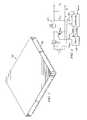
- FIGS. 1 and 2illustrate isometric views of an embodiment of an electronic device, before encapsulation, constructed according to the principles of the present invention
- FIG. 3illustrates an isometric view of an embodiment of an electronic device, after encapsulation, constructed according to the principles of the present invention.
- FIG. 4illustrates a diagram of an embodiment of a power converter including power conversion circuitry constructed according to the principles of the present invention.
- a magnetic devicean electronic device (e.g., a power module) and a method of manufacture thereof.
- the magnetic devicesare also referred to as micromagnetic devices.
- the termsmay be used synonymously. While the principles of the present invention will be described in the environment of a power module, any application that may benefit from a magnetic device as described herein is well within the broad scope of the present invention.
- a magnetic device embodied in an inductoris formed with a magnetic core (e.g., a bar of magnetic material) proximate (e.g., above) a conductive substrate (e.g., an electrically conductive leadframe), and a conductive clip positioned proximate (e.g., above) the magnetic core to complete a winding thereabout (e.g., around).
- a surface (e.g., a lower surface) of the magnetic corefaces (e.g., generally oriented toward) the conductive substrate and a surface (e.g., an upper surface) of the magnetic core faces (e.g., generally oriented toward) the conductive clip.
- the magnetic coreis formed of a medium that generally conducts a given magnetic flux level for a lower level of applied magneto-motive force, such as measured in ampere-turns, compared to a non-magnetic medium such as air (or a vacuum).
- the magnetic coremay occupy a closed flux path such as provided by a torroidal structure, or may occupy a portion of a flux path such as provided by a flat or round bar of magnetic material.
- the magnetic coreincludes structures such as bars and rods, as well as films, and may include multiple layers including intervening layers and layers that improve the magnetic properties thereof.
- an electronic devicesuch as a power module includes other integrated circuits (either in bare die or module form) and surface-mount components coupled (e.g., adhesively mounted) to the conductive substrate and electrically coupled thereto with wire bonds.
- An encapsulantsuch as plastic molded material is placed around the magnetic device, integrated circuit and/or the surface-mount components.
- the power modulemay also include a power conversion circuitry that includes or may be embodied in the magnetic device, the integrated circuit, and at least one surface-mount component. It should be understood that the power module may form, at least in part, a power management system, which itself is often referred to as a power management integrated circuit.
- the power moduleincludes a magnetic device (e.g., inductor), an integrated circuit and surface-mount components.
- the power modulemay include power conversion circuitry that includes or may be embodied in the magnetic device, the integrated circuit and at least one of the surface-mount components.
- the power conversion circuitrymay form a power converter that often includes switching regulators such as buck switching regulators with digital control circuits for reduced component count, and synchronous rectifiers for high power conversion efficiency.
- switching regulatorssuch as buck switching regulators with digital control circuits for reduced component count, and synchronous rectifiers for high power conversion efficiency.
- the broad scope of the present inventionis not limited to a power module, power converter or the like, and may be applicable to other electronic devices.
- a conductive substrate (e.g., conductive leadframe or leadframe) 110is patterned and etched to form an electrically conductive interconnect layer for the lower portion of a winding for the inductor as well as the electrical interconnections among surface-mount components, the integrated circuit, and the inductor.
- a typical thickness of the leadframe 110is about eight mils. While the leadframe 110 is often constructed of copper, alternative electrically conductive materials can be used therefor.
- the leadframe 110provides external connections for the power module, as well as a support base for a magnetic material for the inductor. The external connections are formed as fingers of the leadframe 110 , referenced as leadframe fingers (two of which are designated 115 , 116 ).
- the leadframe 110is generally constructed with an integral strip surrounding the electrically conductive pattern to provide mechanical support during the manufacturing steps, which strip is discarded later in the manufacturing process.
- the surrounding stripis generally sheared off after the electronic device has been constructed.
- the leadframe 110is generally produced in an array of repeating of patterns (not shown), such as a 16 ⁇ 16 array, to form, for example, 256 substantially identical electronic devices. Forming an array of leadframes 110 is a process well known in the art to reduce the manufacturing cost of producing the electronic devices.
- Solder pasteis selectively applied to the leadframe 110 in a thin layer to areas (one of which is designated 125 ) for screening processes, to provide electrical and mechanical attachment for surface-mount components.
- the surface-mount componentssuch as capacitors (one of which is designated 120 ) are placed with their conductive ends in the solder paste.
- the solder pastemay be composed of lead-based as well as lead-free compositions.
- the array of leadframes 110 with the surface-mount components 120is reflowed in an oven to mechanically and electrically attach the surface-mount components 120 to the leadframe 110 .
- the steps as described abovegenerally do not require execution in the highly controlled environment of a clean room.
- the following steps, however,are preferably performed in a clean room environment such as typically used for assembly of integrated circuits into a molded plastic package, as is generally well known in the art.
- An adhesivee.g., a die attach adhesive such as Abletherm 2600AT by Ablestik of Rancho Dominquez, Calif.
- a magnetic coree.g., a bar of magnetic material
- the bar of magnetic material 130 and the semiconductor die 140are positioned on the leadframe 110 over the die attach adhesive.
- a lower surface of the bar of magnetic material 130faces, and is preferably adhered to, the leadframe 110 .
- the bar of magnetic material 130is included to enhance the magnetic properties of the inductor and may be about 250 micrometers ( ⁇ m) thick, four mils wide and 7.5 mils long.
- the adhesiveis cured, typically in a controlled thermal process, to secure the bar of magnetic material 130 and the semiconductor die 140 to the leadframe 110 .
- solder pasteis applied to areas (generally designated 160 ) of the leadframe 110 wherein ends of conductive clips 150 are placed.
- the solder pastemay be composed of lead-based as well as lead-free compositions.
- the conductive clips 150(e.g., about 8-12 mils thick) are placed on the leadframe 110 above the bars of magnetic material 130 with their ends in the solder paste.
- the conductive clips 150are formed with their ends bent toward the leadframe 110 about ends of the bar of magnetic material 130 without mechanical interference. Thus, an upper surface of the bar of magnetic material 130 faces the conductive clips 150 .
- An insulating gapfor example, about a five mil air gap, is thus preferably left between the upper surfaces of the bars of magnetic material 130 and the lower surfaces of the conductive clips 150 , which gap may be filled later by an encapsulant.
- the conductive clips 150provide the portion of the electrically conductive inductor winding above each bar of magnetic material 130 .
- the leadframe 110is heated in a reflow oven to mechanically and electrically bond the conductive clips 150 to the leadframe 110 .
- Wire bonds preferably formed of gold wire such as a first wire bond 165are attached to each semiconductor die 140 and to the leadframe 110 to electrically couple pads on the semiconductor die 140 to bonding areas of the leadframe 110 thereby providing electrical circuit connections therebetween.
- Wire bonds such as a second wire bond 166may also be used to selectively electrically couple portions of the leadframe 110 to provide circuit interconnections that cannot be easily wired in a single planar layout, thus producing the topological layout equivalent for the leadframe 110 of a two-layer printed wiring board or substrate.
- the arrayis placed in a mold, and an encapsulant such as a molding material, preferably epoxy, is deposited (e.g., injected) thereover as is well known in the art to provide environmental and mechanical protection as well as a thermally conductive covering to facilitate heat dissipation during operation.
- an encapsulantsuch as a molding material, preferably epoxy
- a molding materialpreferably epoxy
- Other molding materials and processes as well as electronic devices constructed without an encapsulantare well within the broad scope of the present invention.
- the individual electronic devicesare singulated from the array thereof by a punching and shearing operation to produce an encapsulated power module including power conversion circuitry as illustrated with respect to FIG. 3 .
- the power moduleis mechanically and hermetically protected by the encapsulant 170 as illustrated.
- External electrical connections to a system employing the power moduleare made via terminals 180 which are created from exposed leadframe fingers (see FIG. 1 ) protruding from sides and a lower surface of the power module after encapsulation.
- the terminals 180are substantially coplanar with the sides and lower surface of the power module.
- the terminals 180are formed by the shearing and molding operation on the leadframe 110 as is well known in the art.
- Electrical connections to the system employing the power moduleare made by placing the power module on another circuit board or printed wiring board formed with interconnect pads that are covered with solder paste, generally by a screening operation, and heating the power module on the circuit board in a reflow oven.
- the reflow soldering operationis generally also adequate to provide mechanical attachment of the power module to another printed wiring board, but other attachment methods such as adhesive compound are well within the broad scope of the present invention.
- FIG. 4illustrated is a diagram of an embodiment of a power converter including power conversion circuitry constructed according to the principles of the present invention.
- the power converterincludes a power train 410 , a controller 420 and a driver 430 , and provides power to a system such as a microprocessor. While in the illustrated embodiment, the power train 410 employs a buck converter topology, those skilled in the art should understand that other converter topologies such as a forward converter topology are well within the broad scope of the present invention.
- the power train 410receives an input voltage V in from a source of electrical power (represented by a battery) at an input thereof and provides a regulated output voltage V out to power, for instance, a microprocessor at an output thereof.
- the output voltage V outis generally less than the input voltage V in such that a switching operation of the power converter can regulate the output voltage V out .
- a switche.g., a main switch Q mn
- a switchis enabled to conduct for a primary interval (generally co-existent with a primary duty cycle “D” of the main switch Q mn ) and couples the input voltage V in to an output filter inductor L out .
- an inductor current I Lout flowing through the output filter inductor L outincreases as a current flows from the input to the output of the power train 410 .
- a component of the inductor current I Loutis filtered by the output capacitor C out .
- the main switch Q mnis transitioned to a non-conducting state and another switch (e.g., an auxiliary switch Q aux ) is enabled to conduct.
- the auxiliary switch Q auxprovides a path to maintain a continuity of the inductor current I Lout flowing through the output filter inductor L out .
- the inductor current I Lout through the output filter inductor L outdecreases.
- the duty cycle of the main and auxiliary switches Q mn , Q auxmay be adjusted to maintain a regulation of the output voltage V out of the power converter.
- the conduction periods for the main and auxiliary switches Q mn , Q auxmay be separated by a small time interval to avoid cross conduction therebetween and beneficially to reduce the switching losses associated with the power converter.
- the controller 420receives a desired characteristic such as a desired system voltage V system from an internal or external source associated with the microprocessor, and the output voltage V out of the power converter.
- the controller 420is also coupled to the input voltage V in of the power converter and a return lead of the source of electrical power (again, represented by a battery) to provide a ground connection therefor.
- a decoupling capacitor C decis coupled to the path from the input voltage V in to the controller 420 .
- the decoupling capacitor C decis configured to absorb high frequency noise signals associated with the source of electrical power to protect the controller 420 .
- the controller 420provides a signal (e.g., a pulse width modulated signal S PWM ) to control a duty cycle and a frequency of the main and auxiliary switches Q mn , Q aux of the power train 410 to regulate the output voltage V out thereof.
- the controller 420may also provide a complement of the signal (e.g., a complementary pulse width modulated signal S 1-PWM ) in accordance with the aforementioned characteristics.
- Any controller adapted to control at least one switch of the power converteris well within the broad scope of the present invention.
- a controller employing digital circuitryis disclosed in U.S. Pat. No.
- the power converteralso includes the driver 430 configured to provide drive signals S DRV1 , S DRV2 to the main and auxiliary switches Q mn , Q aux , respectively, based on the signals S PWM , S 1-PWM provided by the controller 420 .
- the driver 430typically includes switching circuitry incorporating a plurality of driver switches that cooperate to provide the drive signals S DRV1 , S DRV2 to the main and auxiliary switches Q mn , Q aux .
- any driver 430capable of providing the drive signals S DRV1 , S DRV2 to control a switch is well within the broad scope of the present invention.
- a driveris disclosed in U.S. Pat. No. 7,330,017, entitled “Driver for a Power Converter and Method of Driving a Switch Thereof,” to Dwarakanath, et al., which is incorporated herein by reference.
- an embodiment of a semiconductor device that may embody portions of the power conversion circuitryis disclosed in U.S. Pat. No.
- a magnetic device, a power module and a method of manufacture thereofwith readily attainable and quantifiable advantages have been introduced.
- Those skilled in the artshould understand that the previously described embodiments of the magnetic device and power module are submitted for illustrative purposes only.
- other embodiments capable of producing a magnetic device and a power module while addressing compact, efficient and high density power modules, while being manufacturable at high volume and with lower cost than is achieved with the prior artare well within the broad scope of the present invention.
- the magnetic devicehas been described in the environment of a power converter, the magnetic device may also be incorporated into other electronic devices, systems or assemblies such as communication or computing devices or other power processing devices.
- the present inventionprovides a magnetic device including a magnetic core having a surface facing a conductive substrate and a conductive clip facing a surface of the magnetic core with ends of the conductive clip electrically coupled to the conductive substrate to cooperatively form a winding therewith about the magnetic core.
- the present inventionprovides an inductor compatible with ordinary manufacturing and packaging processes for power management integrated circuits.
- the inductorincludes a magnetic core formed from a bar of magnetic material adhered to conductive substrate (e.g., a patterned, conductive leadframe) and at least one conductive clip is placed above the bar of magnetic material to complete the portion of the inductor winding above the leadframe.
- the conductive clipis made of copper, but other electrically conductive materials are well within the broad scope of the present invention.
- the bar of magnetic materialis adhered to the leadframe with a die attach adhesive, and the at least one conductive clip is soldered to the leadframe.
- the inductoris preferably encapsulated with plastic encapsulating compound including an epoxy.
- the bar of magnetic materialincludes a ceramic material such as a soft magnetic ferrite having manganese zinc or nickel zinc ferrite.
- the bar of magnetic materialis formed with a metallic alloy such as an iron cobalt alloy deposited via an electroplating process on a semiconductor or insulating die such as a silicon die.
- the at least one conductive clipmay be soldered to the leadframe in a reflow soldering process. Additionally, a gap may be formed between the at least one conductive clip and the bar of magnetic material. In accordance therewith, the gap is typically filled with plastic encapsulating compound.
- the integrated circuitis also adhered to the leadframe.
- the integrated circuitis wire bonded (via, for instance, gold wires) to the leadframe to form electrical connections therebetween. Surface-mount components may also be soldered to the leadframe.
- a magnetic device, integrated circuit and surface-mount componentsare integrated to form an electronic device such as a power module or power management integrated circuit.
- the present inventionprovides methods of forming the magnetic device and power module that take advantage of current practices in the field of power management integrated circuits.
Landscapes
- Engineering & Computer Science (AREA)
- Power Engineering (AREA)
- Microelectronics & Electronic Packaging (AREA)
- Physics & Mathematics (AREA)
- Condensed Matter Physics & Semiconductors (AREA)
- General Physics & Mathematics (AREA)
- Computer Hardware Design (AREA)
- Dc-Dc Converters (AREA)
Abstract
Description
Claims (20)
Priority Applications (1)
| Application Number | Priority Date | Filing Date | Title |
|---|---|---|---|
| US11/243,778US8139362B2 (en) | 2005-10-05 | 2005-10-05 | Power module with a magnetic device having a conductive clip |
Applications Claiming Priority (1)
| Application Number | Priority Date | Filing Date | Title |
|---|---|---|---|
| US11/243,778US8139362B2 (en) | 2005-10-05 | 2005-10-05 | Power module with a magnetic device having a conductive clip |
Publications (2)
| Publication Number | Publication Date |
|---|---|
| US20070075816A1 US20070075816A1 (en) | 2007-04-05 |
| US8139362B2true US8139362B2 (en) | 2012-03-20 |
Family
ID=37901338
Family Applications (1)
| Application Number | Title | Priority Date | Filing Date |
|---|---|---|---|
| US11/243,778Expired - Fee RelatedUS8139362B2 (en) | 2005-10-05 | 2005-10-05 | Power module with a magnetic device having a conductive clip |
Country Status (1)
| Country | Link |
|---|---|
| US (1) | US8139362B2 (en) |
Cited By (4)
| Publication number | Priority date | Publication date | Assignee | Title |
|---|---|---|---|---|
| US8618900B2 (en) | 2007-09-10 | 2013-12-31 | Enpirion, Inc. | Micromagnetic device and method of forming the same |
| US8631560B2 (en) | 2005-10-05 | 2014-01-21 | Enpirion, Inc. | Method of forming a magnetic device having a conductive clip |
| US8701272B2 (en) | 2005-10-05 | 2014-04-22 | Enpirion, Inc. | Method of forming a power module with a magnetic device having a conductive clip |
| US11317545B1 (en) | 2020-10-26 | 2022-04-26 | Modular Power Technology, Inc. | Apparatus for an inductor disposed in a band for method of heat dispersion |
Families Citing this family (21)
| Publication number | Priority date | Publication date | Assignee | Title |
|---|---|---|---|---|
| US7462317B2 (en)* | 2004-11-10 | 2008-12-09 | Enpirion, Inc. | Method of manufacturing an encapsulated package for a magnetic device |
| US7426780B2 (en)* | 2004-11-10 | 2008-09-23 | Enpirion, Inc. | Method of manufacturing a power module |
| US8139362B2 (en)* | 2005-10-05 | 2012-03-20 | Enpirion, Inc. | Power module with a magnetic device having a conductive clip |
| US7688172B2 (en)* | 2005-10-05 | 2010-03-30 | Enpirion, Inc. | Magnetic device having a conductive clip |
| US8133529B2 (en)* | 2007-09-10 | 2012-03-13 | Enpirion, Inc. | Method of forming a micromagnetic device |
| US7952459B2 (en) | 2007-09-10 | 2011-05-31 | Enpirion, Inc. | Micromagnetic device and method of forming the same |
| US7955868B2 (en)* | 2007-09-10 | 2011-06-07 | Enpirion, Inc. | Method of forming a micromagnetic device |
| US8018315B2 (en)* | 2007-09-10 | 2011-09-13 | Enpirion, Inc. | Power converter employing a micromagnetic device |
| US8692532B2 (en) | 2008-04-16 | 2014-04-08 | Enpirion, Inc. | Power converter with controller operable in selected modes of operation |
| US8686698B2 (en) | 2008-04-16 | 2014-04-01 | Enpirion, Inc. | Power converter with controller operable in selected modes of operation |
| US8541991B2 (en) | 2008-04-16 | 2013-09-24 | Enpirion, Inc. | Power converter with controller operable in selected modes of operation |
| US9246390B2 (en) | 2008-04-16 | 2016-01-26 | Enpirion, Inc. | Power converter with controller operable in selected modes of operation |
| US8153473B2 (en)* | 2008-10-02 | 2012-04-10 | Empirion, Inc. | Module having a stacked passive element and method of forming the same |
| US9054086B2 (en)* | 2008-10-02 | 2015-06-09 | Enpirion, Inc. | Module having a stacked passive element and method of forming the same |
| US8266793B2 (en)* | 2008-10-02 | 2012-09-18 | Enpirion, Inc. | Module having a stacked magnetic device and semiconductor device and method of forming the same |
| US8339802B2 (en)* | 2008-10-02 | 2012-12-25 | Enpirion, Inc. | Module having a stacked magnetic device and semiconductor device and method of forming the same |
| US9548714B2 (en) | 2008-12-29 | 2017-01-17 | Altera Corporation | Power converter with a dynamically configurable controller and output filter |
| US8698463B2 (en)* | 2008-12-29 | 2014-04-15 | Enpirion, Inc. | Power converter with a dynamically configurable controller based on a power conversion mode |
| US8867295B2 (en) | 2010-12-17 | 2014-10-21 | Enpirion, Inc. | Power converter for a memory module |
| TWI438792B (en) | 2011-01-04 | 2014-05-21 | Cyntec Co Ltd | Inductor |
| US9509217B2 (en) | 2015-04-20 | 2016-11-29 | Altera Corporation | Asymmetric power flow controller for a power converter and method of operating the same |
Citations (161)
| Publication number | Priority date | Publication date | Assignee | Title |
|---|---|---|---|---|
| US1889398A (en) | 1932-03-05 | 1932-11-29 | Western Electric Co | Electrical coil and a method of manufacturing it |
| US2600473A (en) | 1949-01-26 | 1952-06-17 | Philips Lab Inc | Magnetic core |
| US3210707A (en) | 1962-10-04 | 1965-10-05 | Gen Instrument Corp | Solid state inductor built up of multiple thin films |
| US3691497A (en) | 1970-10-15 | 1972-09-12 | Us Army | Leadless microminiature inductance element with a closed magnetic circuit |
| US3762039A (en) | 1971-09-10 | 1973-10-02 | Mos Technology Inc | Plastic encapsulation of microcircuits |
| US3902148A (en)* | 1970-11-27 | 1975-08-26 | Signetics Corp | Semiconductor lead structure and assembly and method for fabricating same |
| US3908264A (en) | 1974-04-24 | 1975-09-30 | Gen Instrument Corp | Method for calibrating a resonant frequency |
| US3947699A (en) | 1974-08-29 | 1976-03-30 | Iowa State University Research Foundation, Inc. | Apparatus for selecting a predetermined portion of an analog signal and gating it to an output |
| US4101389A (en) | 1976-05-20 | 1978-07-18 | Sony Corporation | Method of manufacturing amorphous alloy |
| US4103267A (en)* | 1977-06-13 | 1978-07-25 | Burr-Brown Research Corporation | Hybrid transformer device |
| US4187128A (en) | 1978-09-26 | 1980-02-05 | Bell Telephone Laboratories, Incorporated | Magnetic devices including amorphous alloys |
| US4199743A (en) | 1978-02-06 | 1980-04-22 | Westinghouse Electric Corp. | Encapsulated current transformer |
| GB2041818A (en) | 1979-02-10 | 1980-09-17 | Plessey Co Ltd | Encapsulating a Magnetic Domain Component |
| US4433927A (en) | 1981-02-25 | 1984-02-28 | Honeywell Information Systems Italia | Electromagnet assembly for mosaic printing head and related manufacturing method |
| US4586436A (en)* | 1984-09-13 | 1986-05-06 | The United States Of America As Represented By The Secretary Of The Navy | Electronic assembly for moderate hard target penetrator fuze |
| US4636752A (en) | 1984-06-08 | 1987-01-13 | Murata Manufacturing Co., Ltd. | Noise filter |
| US4668310A (en) | 1979-09-21 | 1987-05-26 | Hitachi Metals, Ltd. | Amorphous alloys |
| US4681718A (en) | 1984-05-09 | 1987-07-21 | Hughes Aircraft Company | Method of fabricating composite or encapsulated articles |
| US4751199A (en) | 1983-12-06 | 1988-06-14 | Fairchild Semiconductor Corporation | Process of forming a compliant lead frame for array-type semiconductor packages |
| US4754317A (en)* | 1986-04-28 | 1988-06-28 | Monolithic Memories, Inc. | Integrated circuit die-to-lead frame interconnection assembly and method |
| US4777465A (en) | 1986-04-28 | 1988-10-11 | Burr-Brown Corporation | Square toroid transformer for hybrid integrated circuit |
| US4808118A (en)* | 1987-11-25 | 1989-02-28 | Itt Corporation | Retention and ground plane connector clip |
| US4870224A (en) | 1988-07-01 | 1989-09-26 | Intel Corporation | Integrated circuit package for surface mount technology |
| US4916522A (en) | 1988-04-21 | 1990-04-10 | American Telephone And Telegraph Company , At & T Bell Laboratories | Integrated circuit package using plastic encapsulant |
| US4975671A (en)* | 1988-08-31 | 1990-12-04 | Apple Computer, Inc. | Transformer for use with surface mounting technology |
| US5056214A (en) | 1989-12-19 | 1991-10-15 | Mark Iv Industries, Inc | Method of making a molded transformer enclosure |
| US5059278A (en) | 1990-09-28 | 1991-10-22 | Seagate Technology | Selective chemical removal of coil seed-layer in thin film head magnetic transducer |
| US5096513A (en) | 1989-09-01 | 1992-03-17 | Kabushiki Kaisha Toshiba | Very thin soft magnetic alloy strips and magnetic core and electromagnetic apparatus made therefrom |
| US5118298A (en) | 1991-04-04 | 1992-06-02 | Advanced Interconnections Corporation | Through hole mounting of integrated circuit adapter leads |
| US5161098A (en) | 1991-09-09 | 1992-11-03 | Power Integrations, Inc. | High frequency switched mode converter |
| US5187119A (en) | 1991-02-11 | 1993-02-16 | The Boeing Company | Multichip module and integrated circuit substrates having planarized patterned surfaces |
| US5262296A (en) | 1988-03-30 | 1993-11-16 | Toray Industries, Inc. | Freeze-dried composition containing enzyme-labeled anti-human interferon-β antibody and enzyme immunoassay kit containing the composition |
| US5279988A (en) | 1992-03-31 | 1994-01-18 | Irfan Saadat | Process for making microcomponents integrated circuits |
| US5285369A (en) | 1992-09-01 | 1994-02-08 | Power Integrations, Inc. | Switched mode power supply integrated circuit with start-up self-biasing |
| US5345670A (en) | 1992-12-11 | 1994-09-13 | At&T Bell Laboratories | Method of making a surface-mount power magnetic device |
| US5353001A (en) | 1991-01-24 | 1994-10-04 | Burr-Brown Corporation | Hybrid integrated circuit planar transformer |
| US5428245A (en) | 1994-05-06 | 1995-06-27 | National Semiconductor Corporation | Lead frame including an inductor or other such magnetic component |
| US5436409A (en) | 1991-01-10 | 1995-07-25 | Sumitomo Electric Industries, Ltd. | Electrical conductor member such as a wire with an inorganic insulating coating |
| US5469334A (en) | 1991-09-09 | 1995-11-21 | Power Integrations, Inc. | Plastic quad-packaged switched-mode integrated circuit with integrated transformer windings and mouldings for transformer core pieces |
| US5484494A (en) | 1992-05-14 | 1996-01-16 | Mitsubishi Rayon Company, Inc. | Amorphous alloy and method for its production |
| US5524334A (en) | 1990-03-13 | 1996-06-11 | Boesel; Robert P. | Method of making an encapsulated high efficiency transformer and power supply |
| US5561438A (en) | 1991-11-13 | 1996-10-01 | Seiko Epson Corporation | Ferrite Antenna |
| US5574420A (en)* | 1994-05-27 | 1996-11-12 | Lucent Technologies Inc. | Low profile surface mounted magnetic devices and components therefor |
| US5574273A (en)* | 1993-06-14 | 1996-11-12 | Hitachi Maxell, Ltd. | Non-contact system parallel data transfer system |
| US5578261A (en) | 1993-05-17 | 1996-11-26 | Lucent Technologies Inc. | Method of encapsulating large substrate devices using reservoir cavities for balanced mold filling |
| US5692296A (en) | 1993-08-18 | 1997-12-02 | Lsi Logic Corporation | Method for encapsulating an integrated circuit package |
| US5783025A (en)* | 1994-06-07 | 1998-07-21 | Texas Instruments Incorporated | Optical diebonding for semiconductor devices |
| US5788854A (en) | 1993-08-16 | 1998-08-04 | California Micro Devices Corporation | Methods for fabrication of thin film inductors, inductor networks, inductor/capactor filters, and integration with other passive and active devices, and the resultant devices |
| US5787569A (en) | 1996-02-21 | 1998-08-04 | Lucent Technologies Inc. | Encapsulated package for power magnetic devices and method of manufacture therefor |
| US5802702A (en) | 1994-06-30 | 1998-09-08 | Lucent Technologies Inc. | Method of making a device including a metallized magnetic substrate |
| US5807959A (en)* | 1995-12-21 | 1998-09-15 | National Starch And Chemical Investment Holding Corporation | Flexible epoxy adhesives with low bleeding tendency |
| US5834691A (en)* | 1995-01-19 | 1998-11-10 | Sharp Kabushiki Kaisha | Lead frame, its use in the fabrication of resin-encapsulated semiconductor device |
| US5835350A (en) | 1996-12-23 | 1998-11-10 | Lucent Technologies Inc. | Encapsulated, board-mountable power supply and method of manufacture therefor |
| US5837155A (en) | 1995-08-28 | 1998-11-17 | Taiyo Ink Manufacturing Co., Ltd. | Insulating resin composition for build-up by copper foil lamination and method for production of multilayer printed circuit board using the composition |
| US5846441A (en) | 1995-09-30 | 1998-12-08 | Daewoo Electronics Co., Ltd. | Method for forming a patterned metallic layer in a thin film magnetic head |
| US5898991A (en) | 1997-01-16 | 1999-05-04 | International Business Machines Corporation | Methods of fabrication of coaxial vias and magnetic devices |
| US5920249A (en)* | 1997-10-30 | 1999-07-06 | Ford Motor Company | Protective method of support for an electromagnetic apparatus |
| US5973923A (en)* | 1998-05-28 | 1999-10-26 | Jitaru; Ionel | Packaging power converters |
| US5998925A (en)* | 1996-07-29 | 1999-12-07 | Nichia Kagaku Kogyo Kabushiki Kaisha | Light emitting device having a nitride compound semiconductor and a phosphor containing a garnet fluorescent material |
| US6005377A (en) | 1997-09-17 | 1999-12-21 | Lucent Technologies Inc. | Programmable digital controller for switch mode power conversion and power supply employing the same |
| US6005467A (en) | 1997-02-11 | 1999-12-21 | Pulse Engineering, Inc. | Trimmable inductor |
| US6060176A (en) | 1995-11-30 | 2000-05-09 | International Business Machines Corporation | Corrosion protection for metallic features |
| US6081997A (en) | 1997-08-14 | 2000-07-04 | Lsi Logic Corporation | System and method for packaging an integrated circuit using encapsulant injection |
| US6087920A (en) | 1997-02-11 | 2000-07-11 | Pulse Engineering, Inc. | Monolithic inductor |
| US6087921A (en) | 1998-10-06 | 2000-07-11 | Pulse Engineering, Inc. | Placement insensitive monolithic inductor and method of manufacturing same |
| US6094123A (en) | 1998-09-25 | 2000-07-25 | Lucent Technologies Inc. | Low profile surface mount chip inductor |
| US6101218A (en) | 1994-06-27 | 2000-08-08 | Advantest Corp. | Leakage power measurement apparatus and method |
| US6118351A (en) | 1997-06-10 | 2000-09-12 | Lucent Technologies Inc. | Micromagnetic device for power processing applications and method of manufacture therefor |
| US6118360A (en)* | 1996-01-11 | 2000-09-12 | Systems, Machines, Automation Components Corporation | Linear actuator |
| US6255714B1 (en) | 1999-06-22 | 2001-07-03 | Agere Systems Guardian Corporation | Integrated circuit having a micromagnetic device including a ferromagnetic core and method of manufacture therefor |
| US20010030595A1 (en) | 2000-03-14 | 2001-10-18 | Junichi Hamatani | Inductor and method for manufacturing same |
| US20010041384A1 (en)* | 1998-05-12 | 2001-11-15 | Mitsubishi Denki Kabushiki Kaisha | Method of producing semiconductor device and configuration thereof, and lead frame used in said method |
| US6317948B1 (en) | 1997-08-25 | 2001-11-20 | Agere Systems Guardian Corp. | Embedded thin film passive components |
| US6353379B1 (en) | 2000-02-28 | 2002-03-05 | Lucent Technologies Inc. | Magnetic device employing a winding structure spanning multiple boards and method of manufacture thereof |
| US6366486B1 (en) | 2000-08-29 | 2002-04-02 | Delta Electronics Inc. | Power supply device for enhancing heat-dissipating effect |
| US6440750B1 (en) | 1997-06-10 | 2002-08-27 | Agere Systems Guardian Corporation | Method of making integrated circuit having a micromagnetic device |
| US6448640B2 (en) | 1999-09-02 | 2002-09-10 | Micron Technology, Inc. | Ball array layout in chip assembly |
| US6466454B1 (en)* | 1999-05-18 | 2002-10-15 | Ascom Energy Systems Ag | Component transformer |
| US20020153258A1 (en) | 2000-04-19 | 2002-10-24 | Filas Robert W. | Device comprising micromagnetic components for power applications and process for forming device |
| US6479981B2 (en) | 1998-06-29 | 2002-11-12 | E.O. Schweitzer Manufacturing Co., Inc. | Remote light indication fault indicator with a timed reset circuit and a manual reset circuit |
| US6541819B2 (en) | 2001-05-24 | 2003-04-01 | Agere Systems Inc. | Semiconductor device having non-power enhanced and power enhanced metal oxide semiconductor devices and a method of manufacture therefor |
| US20030062541A1 (en) | 2001-08-28 | 2003-04-03 | Michael Warner | High-frequency chip packages |
| US6549409B1 (en)* | 2000-08-21 | 2003-04-15 | Vlt Corporation | Power converter assembly |
| US6552629B2 (en) | 2000-12-12 | 2003-04-22 | Micrel, Incorporated | Universally stable output filter |
| US20030076662A1 (en) | 1999-05-14 | 2003-04-24 | Sokymat S.A. | Transponder and injection-molded part and method for manufacturing same |
| US6578253B1 (en) | 1991-10-04 | 2003-06-17 | Fmtt, Inc. | Transformer and inductor modules having directly bonded terminals and heat-sink fins |
| US6608332B2 (en)* | 1996-07-29 | 2003-08-19 | Nichia Kagaku Kogyo Kabushiki Kaisha | Light emitting device and display |
| US20030232196A1 (en) | 2002-06-14 | 2003-12-18 | Krishnamurthy Anand | Coated ferromagnetic particles and composite magnetic articles thereof |
| US6691398B2 (en)* | 1999-05-18 | 2004-02-17 | Pulse Engineering | Electronic packaging device and method |
| US6693805B1 (en) | 2002-07-31 | 2004-02-17 | Lockheed Martin Corporation | Ripple cancellation circuit for ultra-low-noise power supplies |
| US6731002B2 (en)* | 2001-05-04 | 2004-05-04 | Ixys Corporation | High frequency power device with a plastic molded package and direct bonded substrate |
| US6747538B2 (en) | 2001-09-28 | 2004-06-08 | Matsushita Electric Industrial Co., Ltd. | Inductance device |
| US20040130428A1 (en)* | 2002-10-31 | 2004-07-08 | Peter Mignano | Surface mount magnetic core winding structure |
| US20040150500A1 (en) | 2001-11-14 | 2004-08-05 | Kiko Frederick J. | Controlled induction device and method of manufacturing |
| US6790379B2 (en) | 1999-09-20 | 2004-09-14 | Tdk Corporation | Magnetic ferrite composition and process of production thereof |
| US20050011672A1 (en) | 2003-07-17 | 2005-01-20 | Alawani Ashish D. | Overmolded MCM with increased surface mount component reliability |
| US6912781B2 (en) | 2000-01-31 | 2005-07-05 | Pulse Engineering, Inc. | Method of manufacturing electronic packaging device with insertable leads |
| US6922130B2 (en)* | 2002-05-24 | 2005-07-26 | Minebea Co., Ltd. | Surface mount coil with edgewise winding |
| US20050168203A1 (en) | 2004-01-29 | 2005-08-04 | Enpirion, Incorporated | Driver for a power converter and a method of driving a switch thereof |
| US20050167756A1 (en) | 2004-01-29 | 2005-08-04 | Enpirion, Incorporated | Laterally diffused metal oxide semiconductor device and method of forming the same |
| US20050169024A1 (en) | 2004-01-29 | 2005-08-04 | Enpirion, Incorporated, A Delaware Corporation | Controller for a power converter and a method of controlling a switch thereof |
| US20050168205A1 (en) | 2004-01-29 | 2005-08-04 | Enpirion, Incorporated | Controller for a power converter and a method of controlling a switch thereof |
| US20050212132A1 (en) | 2004-03-25 | 2005-09-29 | Min-Chih Hsuan | Chip package and process thereof |
| US6989121B2 (en) | 1998-02-05 | 2006-01-24 | Micron Technology, Inc. | Method for encasing plastic array packages |
| US6998952B2 (en) | 2003-12-05 | 2006-02-14 | Freescale Semiconductor, Inc. | Inductive device including bond wires |
| US20060038225A1 (en) | 2004-08-23 | 2006-02-23 | Lotfi Ashraf W | Integrated circuit employable with a power converter |
| US20060040452A1 (en) | 2004-08-23 | 2006-02-23 | Lotfi Ashraf W | Method of forming an integrated circuit incorporating higher voltage devices and low voltage devices therein |
| US20060040449A1 (en) | 2004-08-23 | 2006-02-23 | Lotfi Ashraf W | Method of forming an integrated circuit incorporating higher voltage devices and low voltage devices therein |
| US7020295B2 (en)* | 2001-07-11 | 2006-03-28 | Murata Manufacturing Co., Ltd. | Piezoelectric electroacoustic transducer and manufacturing method of the same |
| US7023315B2 (en) | 2000-04-24 | 2006-04-04 | Chartered Semiconductor Manufacturing Ltd. | High performance RF inductors and transformers using bonding technique |
| US20060097833A1 (en) | 2004-11-10 | 2006-05-11 | Lotfi Ashraf W | Encapsulated package for a magnetic device |
| US20060096087A1 (en) | 2004-11-10 | 2006-05-11 | Lotfi Ashraf W | Method of manufacturing a power module |
| US20060096088A1 (en) | 2004-11-10 | 2006-05-11 | Lotfi Ashraf W | Method of manufacturing an encapsulated package for a magnetic device |
| US20060097831A1 (en) | 2004-11-10 | 2006-05-11 | Lotfi Ashraf W | Power module |
| US20060097832A1 (en) | 2004-11-10 | 2006-05-11 | Lotfi Ashraf W | Encapsulated package for a magnetic device |
| US20060109072A1 (en) | 2002-05-31 | 2006-05-25 | International Rectifier Corporation | Planar transformer arrangement |
| US20060145800A1 (en) | 2004-08-31 | 2006-07-06 | Majid Dadafshar | Precision inductive devices and methods |
| US7101737B2 (en) | 2000-08-28 | 2006-09-05 | Micron Technology, Inc. | Method of encapsulating interconnecting units in packaged microelectronic devices |
| US20060197207A1 (en) | 2005-02-22 | 2006-09-07 | Stats Chippac Ltd. | Integrated circuit package system with die and package combination |
| US20070025092A1 (en) | 2005-08-01 | 2007-02-01 | Baik-Woo Lee | Embedded actives and discrete passives in a cavity within build-up layers |
| US7175718B2 (en) | 2001-06-19 | 2007-02-13 | Mitsubishi Denki Kabushiki Kaisha | Rare earth element permanent magnet material |
| US20070075815A1 (en)* | 2005-10-05 | 2007-04-05 | Lotfi Ashraf W | Method of forming a magnetic device having a conductive clip |
| US20070075817A1 (en)* | 2005-10-05 | 2007-04-05 | Lotfi Ashraf W | Magnetic device having a conductive clip |
| US20070075816A1 (en)* | 2005-10-05 | 2007-04-05 | Lotfi Ashraf W | Power module with a magnetic device having a conductive clip |
| US20070074386A1 (en)* | 2005-10-05 | 2007-04-05 | Lotfi Ashraf W | Method of forming a power module with a magnetic device having a conductive clip |
| US7214985B2 (en) | 2004-08-23 | 2007-05-08 | Enpirion, Inc. | Integrated circuit incorporating higher voltage devices and low voltage devices therein |
| US7230316B2 (en) | 2002-12-27 | 2007-06-12 | Semiconductor Energy Laboratory Co., Ltd. | Semiconductor device having transferred integrated circuit |
| US7236086B1 (en)* | 1993-06-14 | 2007-06-26 | Vlt, Inc. | Power converter configuration, control, and construction |
| US7250842B1 (en)* | 2005-08-09 | 2007-07-31 | National Semiconductor Corporation | MEMS inductor with very low resistance |
| US20070246808A1 (en) | 2005-03-16 | 2007-10-25 | Henrik Ewe | Power semiconductor module having surface-mountable flat external contacts and method for producing the same |
| US7297631B2 (en) | 2002-06-25 | 2007-11-20 | Unitive International Limited | Methods of forming electronic structures including conductive shunt layers and related structures |
| US20080001701A1 (en) | 2006-06-30 | 2008-01-03 | Gardner Donald S | Control of eddy currents in magnetic vias for inductors and transformers in integrated circuits |
| US20080090079A1 (en) | 2006-09-28 | 2008-04-17 | Fajardo Arnel M | High-resistivity magnetic film from nano-particle plating |
| US7434306B2 (en) | 1999-11-23 | 2008-10-14 | Intel Corporation | Integrated transformer |
| US20080258274A1 (en) | 2005-01-20 | 2008-10-23 | Infineon Technologies Ag | Semiconductor Package and Method |
| US20080258278A1 (en) | 2002-04-29 | 2008-10-23 | Mary Jean Ramos | Partially patterned lead frames and methods of making and using the same in semiconductor packaging |
| US20080303131A1 (en) | 2007-06-11 | 2008-12-11 | Vertical Circuits, Inc. | Electrically interconnected stacked die assemblies |
| US20090004774A1 (en) | 2007-06-27 | 2009-01-01 | Ming Hsun Lee | Method of multi-chip packaging in a tsop package |
| US7498522B2 (en) | 2006-01-30 | 2009-03-03 | Fujitsu Limited | Multilayer printed circuit board and manufacturing method thereof |
| US20090057822A1 (en) | 2007-09-05 | 2009-03-05 | Yenting Wen | Semiconductor component and method of manufacture |
| US20090068347A1 (en) | 2007-09-10 | 2009-03-12 | Lotfi Ashraf W | Method of Forming a Micromagnetic Device |
| US7521907B2 (en) | 2006-03-06 | 2009-04-21 | Enpirion, Inc. | Controller for a power converter and method of operating the same |
| US7544995B2 (en) | 2007-09-10 | 2009-06-09 | Enpirion, Inc. | Power converter employing a micromagnetic device |
| US20090146297A1 (en) | 2007-12-06 | 2009-06-11 | Stats Chippac, Ltd. | Semiconductor Device and Method of Forming Wafer Level Ground Plane and Power Ring |
| US7642762B2 (en) | 2007-01-29 | 2010-01-05 | Linear Technology Corporation | Current source with indirect load current signal extraction |
| US20100084750A1 (en) | 2008-10-02 | 2010-04-08 | Lotfi Ashraf W | Module having a stacked passive element and method of forming the same |
| US20100087036A1 (en) | 2008-10-02 | 2010-04-08 | Lotfi Ashraf W | Module having a stacked passive element and method of forming the same |
| US20100164650A1 (en) | 2008-12-29 | 2010-07-01 | Ahmed Mohamed Abou-Alfotouh | Power Converter with a Dynamically Configurable Controller and Output Filter |
| US20100164449A1 (en) | 2008-12-29 | 2010-07-01 | Mirmira Ramarao Dwarakanath | Power Converter with a Dynamically Configurable Controller and Output Filter |
| US20100214746A1 (en) | 2008-10-02 | 2010-08-26 | Lotfi Ashraf W | Module Having a Stacked Magnetic Device and Semiconductor Device and Method of Forming the Same |
| US20100212150A1 (en) | 2008-10-02 | 2010-08-26 | Lotfi Ashraf W | Module Having a Stacked Magnetic Device and Semiconductor Device and Method of Forming the Same |
| US7786837B2 (en) | 2007-06-12 | 2010-08-31 | Alpha And Omega Semiconductor Incorporated | Semiconductor power device having a stacked discrete inductor structure |
| US7791440B2 (en) | 2004-06-09 | 2010-09-07 | Agency For Science, Technology And Research | Microfabricated system for magnetic field generation and focusing |
| US7876572B2 (en) | 2006-01-27 | 2011-01-25 | Sharp Kabushiki Kaisha | Wiring board and semiconductor apparatus |
| US7920042B2 (en) | 2007-09-10 | 2011-04-05 | Enpirion, Inc. | Micromagnetic device and method of forming the same |
| US7936160B1 (en) | 2007-04-25 | 2011-05-03 | National Semiconductor Corporation | Apparatus and method for valley emulated current mode control |
| US7948772B2 (en) | 2006-07-04 | 2011-05-24 | Orient Semiconductor Electronics | Memory card with electrostatic discharge protection and manufacturing method thereof |
| US7952459B2 (en) | 2007-09-10 | 2011-05-31 | Enpirion, Inc. | Micromagnetic device and method of forming the same |
| US7955868B2 (en) | 2007-09-10 | 2011-06-07 | Enpirion, Inc. | Method of forming a micromagnetic device |
| US7974103B2 (en) | 2006-09-13 | 2011-07-05 | Samsung Electronics Co., Ltd. | LCD signal transfer members |
| US8018315B2 (en) | 2007-09-10 | 2011-09-13 | Enpirion, Inc. | Power converter employing a micromagnetic device |
- 2005
- 2005-10-05USUS11/243,778patent/US8139362B2/ennot_activeExpired - Fee Related
Patent Citations (186)
| Publication number | Priority date | Publication date | Assignee | Title |
|---|---|---|---|---|
| US1889398A (en) | 1932-03-05 | 1932-11-29 | Western Electric Co | Electrical coil and a method of manufacturing it |
| US2600473A (en) | 1949-01-26 | 1952-06-17 | Philips Lab Inc | Magnetic core |
| US3210707A (en) | 1962-10-04 | 1965-10-05 | Gen Instrument Corp | Solid state inductor built up of multiple thin films |
| US3691497A (en) | 1970-10-15 | 1972-09-12 | Us Army | Leadless microminiature inductance element with a closed magnetic circuit |
| US3902148A (en)* | 1970-11-27 | 1975-08-26 | Signetics Corp | Semiconductor lead structure and assembly and method for fabricating same |
| US3762039A (en) | 1971-09-10 | 1973-10-02 | Mos Technology Inc | Plastic encapsulation of microcircuits |
| US3908264A (en) | 1974-04-24 | 1975-09-30 | Gen Instrument Corp | Method for calibrating a resonant frequency |
| US3947699A (en) | 1974-08-29 | 1976-03-30 | Iowa State University Research Foundation, Inc. | Apparatus for selecting a predetermined portion of an analog signal and gating it to an output |
| US4101389A (en) | 1976-05-20 | 1978-07-18 | Sony Corporation | Method of manufacturing amorphous alloy |
| US4103267A (en)* | 1977-06-13 | 1978-07-25 | Burr-Brown Research Corporation | Hybrid transformer device |
| US4199743A (en) | 1978-02-06 | 1980-04-22 | Westinghouse Electric Corp. | Encapsulated current transformer |
| US4187128A (en) | 1978-09-26 | 1980-02-05 | Bell Telephone Laboratories, Incorporated | Magnetic devices including amorphous alloys |
| GB2041818A (en) | 1979-02-10 | 1980-09-17 | Plessey Co Ltd | Encapsulating a Magnetic Domain Component |
| US4668310A (en) | 1979-09-21 | 1987-05-26 | Hitachi Metals, Ltd. | Amorphous alloys |
| US4433927A (en) | 1981-02-25 | 1984-02-28 | Honeywell Information Systems Italia | Electromagnet assembly for mosaic printing head and related manufacturing method |
| US4751199A (en) | 1983-12-06 | 1988-06-14 | Fairchild Semiconductor Corporation | Process of forming a compliant lead frame for array-type semiconductor packages |
| US4681718A (en) | 1984-05-09 | 1987-07-21 | Hughes Aircraft Company | Method of fabricating composite or encapsulated articles |
| US4636752A (en) | 1984-06-08 | 1987-01-13 | Murata Manufacturing Co., Ltd. | Noise filter |
| US4586436A (en)* | 1984-09-13 | 1986-05-06 | The United States Of America As Represented By The Secretary Of The Navy | Electronic assembly for moderate hard target penetrator fuze |
| US4754317A (en)* | 1986-04-28 | 1988-06-28 | Monolithic Memories, Inc. | Integrated circuit die-to-lead frame interconnection assembly and method |
| US4777465A (en) | 1986-04-28 | 1988-10-11 | Burr-Brown Corporation | Square toroid transformer for hybrid integrated circuit |
| US4847986A (en) | 1986-07-02 | 1989-07-18 | Burr Brown Corporation | Method of making square toroid transformer for hybrid integrated circuit |
| US4808118A (en)* | 1987-11-25 | 1989-02-28 | Itt Corporation | Retention and ground plane connector clip |
| US5262296A (en) | 1988-03-30 | 1993-11-16 | Toray Industries, Inc. | Freeze-dried composition containing enzyme-labeled anti-human interferon-β antibody and enzyme immunoassay kit containing the composition |
| US4916522A (en) | 1988-04-21 | 1990-04-10 | American Telephone And Telegraph Company , At & T Bell Laboratories | Integrated circuit package using plastic encapsulant |
| US4870224A (en) | 1988-07-01 | 1989-09-26 | Intel Corporation | Integrated circuit package for surface mount technology |
| US4975671A (en)* | 1988-08-31 | 1990-12-04 | Apple Computer, Inc. | Transformer for use with surface mounting technology |
| US5096513A (en) | 1989-09-01 | 1992-03-17 | Kabushiki Kaisha Toshiba | Very thin soft magnetic alloy strips and magnetic core and electromagnetic apparatus made therefrom |
| US5056214A (en) | 1989-12-19 | 1991-10-15 | Mark Iv Industries, Inc | Method of making a molded transformer enclosure |
| US5524334A (en) | 1990-03-13 | 1996-06-11 | Boesel; Robert P. | Method of making an encapsulated high efficiency transformer and power supply |
| US5059278A (en) | 1990-09-28 | 1991-10-22 | Seagate Technology | Selective chemical removal of coil seed-layer in thin film head magnetic transducer |
| US5436409A (en) | 1991-01-10 | 1995-07-25 | Sumitomo Electric Industries, Ltd. | Electrical conductor member such as a wire with an inorganic insulating coating |
| US5353001A (en) | 1991-01-24 | 1994-10-04 | Burr-Brown Corporation | Hybrid integrated circuit planar transformer |
| US5187119A (en) | 1991-02-11 | 1993-02-16 | The Boeing Company | Multichip module and integrated circuit substrates having planarized patterned surfaces |
| US5118298A (en) | 1991-04-04 | 1992-06-02 | Advanced Interconnections Corporation | Through hole mounting of integrated circuit adapter leads |
| US5469334A (en) | 1991-09-09 | 1995-11-21 | Power Integrations, Inc. | Plastic quad-packaged switched-mode integrated circuit with integrated transformer windings and mouldings for transformer core pieces |
| US5161098A (en) | 1991-09-09 | 1992-11-03 | Power Integrations, Inc. | High frequency switched mode converter |
| US6578253B1 (en) | 1991-10-04 | 2003-06-17 | Fmtt, Inc. | Transformer and inductor modules having directly bonded terminals and heat-sink fins |
| US5561438A (en) | 1991-11-13 | 1996-10-01 | Seiko Epson Corporation | Ferrite Antenna |
| US5279988A (en) | 1992-03-31 | 1994-01-18 | Irfan Saadat | Process for making microcomponents integrated circuits |
| US5484494A (en) | 1992-05-14 | 1996-01-16 | Mitsubishi Rayon Company, Inc. | Amorphous alloy and method for its production |
| US5285369A (en) | 1992-09-01 | 1994-02-08 | Power Integrations, Inc. | Switched mode power supply integrated circuit with start-up self-biasing |
| US5345670A (en) | 1992-12-11 | 1994-09-13 | At&T Bell Laboratories | Method of making a surface-mount power magnetic device |
| US5578261A (en) | 1993-05-17 | 1996-11-26 | Lucent Technologies Inc. | Method of encapsulating large substrate devices using reservoir cavities for balanced mold filling |
| US7236086B1 (en)* | 1993-06-14 | 2007-06-26 | Vlt, Inc. | Power converter configuration, control, and construction |
| US5574273A (en)* | 1993-06-14 | 1996-11-12 | Hitachi Maxell, Ltd. | Non-contact system parallel data transfer system |
| US5788854A (en) | 1993-08-16 | 1998-08-04 | California Micro Devices Corporation | Methods for fabrication of thin film inductors, inductor networks, inductor/capactor filters, and integration with other passive and active devices, and the resultant devices |
| US5692296A (en) | 1993-08-18 | 1997-12-02 | Lsi Logic Corporation | Method for encapsulating an integrated circuit package |
| US5428245A (en) | 1994-05-06 | 1995-06-27 | National Semiconductor Corporation | Lead frame including an inductor or other such magnetic component |
| US5574420A (en)* | 1994-05-27 | 1996-11-12 | Lucent Technologies Inc. | Low profile surface mounted magnetic devices and components therefor |
| US5783025A (en)* | 1994-06-07 | 1998-07-21 | Texas Instruments Incorporated | Optical diebonding for semiconductor devices |
| US6101218A (en) | 1994-06-27 | 2000-08-08 | Advantest Corp. | Leakage power measurement apparatus and method |
| US5802702A (en) | 1994-06-30 | 1998-09-08 | Lucent Technologies Inc. | Method of making a device including a metallized magnetic substrate |
| US5834691A (en)* | 1995-01-19 | 1998-11-10 | Sharp Kabushiki Kaisha | Lead frame, its use in the fabrication of resin-encapsulated semiconductor device |
| US5837155A (en) | 1995-08-28 | 1998-11-17 | Taiyo Ink Manufacturing Co., Ltd. | Insulating resin composition for build-up by copper foil lamination and method for production of multilayer printed circuit board using the composition |
| US5846441A (en) | 1995-09-30 | 1998-12-08 | Daewoo Electronics Co., Ltd. | Method for forming a patterned metallic layer in a thin film magnetic head |
| US6060176A (en) | 1995-11-30 | 2000-05-09 | International Business Machines Corporation | Corrosion protection for metallic features |
| US5807959A (en)* | 1995-12-21 | 1998-09-15 | National Starch And Chemical Investment Holding Corporation | Flexible epoxy adhesives with low bleeding tendency |
| US6118360A (en)* | 1996-01-11 | 2000-09-12 | Systems, Machines, Automation Components Corporation | Linear actuator |
| US5787569A (en) | 1996-02-21 | 1998-08-04 | Lucent Technologies Inc. | Encapsulated package for power magnetic devices and method of manufacture therefor |
| US6608332B2 (en)* | 1996-07-29 | 2003-08-19 | Nichia Kagaku Kogyo Kabushiki Kaisha | Light emitting device and display |
| US5998925A (en)* | 1996-07-29 | 1999-12-07 | Nichia Kagaku Kogyo Kabushiki Kaisha | Light emitting device having a nitride compound semiconductor and a phosphor containing a garnet fluorescent material |
| US5835350A (en) | 1996-12-23 | 1998-11-10 | Lucent Technologies Inc. | Encapsulated, board-mountable power supply and method of manufacture therefor |
| US5898991A (en) | 1997-01-16 | 1999-05-04 | International Business Machines Corporation | Methods of fabrication of coaxial vias and magnetic devices |
| US6005467A (en) | 1997-02-11 | 1999-12-21 | Pulse Engineering, Inc. | Trimmable inductor |
| US6087920A (en) | 1997-02-11 | 2000-07-11 | Pulse Engineering, Inc. | Monolithic inductor |
| US6440750B1 (en) | 1997-06-10 | 2002-08-27 | Agere Systems Guardian Corporation | Method of making integrated circuit having a micromagnetic device |
| US6118351A (en) | 1997-06-10 | 2000-09-12 | Lucent Technologies Inc. | Micromagnetic device for power processing applications and method of manufacture therefor |
| US6160721A (en) | 1997-06-10 | 2000-12-12 | Lucent Technologies Inc. | Micromagnetic device for power processing applications and method of manufacture therefor |
| US7021518B2 (en) | 1997-06-10 | 2006-04-04 | Agere Systems Inc. | Micromagnetic device for power processing applications and method of manufacture therefor |
| US6081997A (en) | 1997-08-14 | 2000-07-04 | Lsi Logic Corporation | System and method for packaging an integrated circuit using encapsulant injection |
| US6317948B1 (en) | 1997-08-25 | 2001-11-20 | Agere Systems Guardian Corp. | Embedded thin film passive components |
| US6005377A (en) | 1997-09-17 | 1999-12-21 | Lucent Technologies Inc. | Programmable digital controller for switch mode power conversion and power supply employing the same |
| US5920249A (en)* | 1997-10-30 | 1999-07-06 | Ford Motor Company | Protective method of support for an electromagnetic apparatus |
| US6989121B2 (en) | 1998-02-05 | 2006-01-24 | Micron Technology, Inc. | Method for encasing plastic array packages |
| US20010041384A1 (en)* | 1998-05-12 | 2001-11-15 | Mitsubishi Denki Kabushiki Kaisha | Method of producing semiconductor device and configuration thereof, and lead frame used in said method |
| US5973923A (en)* | 1998-05-28 | 1999-10-26 | Jitaru; Ionel | Packaging power converters |
| US6479981B2 (en) | 1998-06-29 | 2002-11-12 | E.O. Schweitzer Manufacturing Co., Inc. | Remote light indication fault indicator with a timed reset circuit and a manual reset circuit |
| US6094123A (en) | 1998-09-25 | 2000-07-25 | Lucent Technologies Inc. | Low profile surface mount chip inductor |
| US6087921A (en) | 1998-10-06 | 2000-07-11 | Pulse Engineering, Inc. | Placement insensitive monolithic inductor and method of manufacturing same |
| US20030076662A1 (en) | 1999-05-14 | 2003-04-24 | Sokymat S.A. | Transponder and injection-molded part and method for manufacturing same |
| US6466454B1 (en)* | 1999-05-18 | 2002-10-15 | Ascom Energy Systems Ag | Component transformer |
| US6691398B2 (en)* | 1999-05-18 | 2004-02-17 | Pulse Engineering | Electronic packaging device and method |
| US6649422B2 (en) | 1999-06-22 | 2003-11-18 | Agere Systems Inc. | Integrated circuit having a micromagnetic device and method of manufacture therefor |
| US6255714B1 (en) | 1999-06-22 | 2001-07-03 | Agere Systems Guardian Corporation | Integrated circuit having a micromagnetic device including a ferromagnetic core and method of manufacture therefor |
| US6448640B2 (en) | 1999-09-02 | 2002-09-10 | Micron Technology, Inc. | Ball array layout in chip assembly |
| US6790379B2 (en) | 1999-09-20 | 2004-09-14 | Tdk Corporation | Magnetic ferrite composition and process of production thereof |
| US7434306B2 (en) | 1999-11-23 | 2008-10-14 | Intel Corporation | Integrated transformer |
| US6912781B2 (en) | 2000-01-31 | 2005-07-05 | Pulse Engineering, Inc. | Method of manufacturing electronic packaging device with insertable leads |
| US6353379B1 (en) | 2000-02-28 | 2002-03-05 | Lucent Technologies Inc. | Magnetic device employing a winding structure spanning multiple boards and method of manufacture thereof |
| US20010030595A1 (en) | 2000-03-14 | 2001-10-18 | Junichi Hamatani | Inductor and method for manufacturing same |
| US20020153258A1 (en) | 2000-04-19 | 2002-10-24 | Filas Robert W. | Device comprising micromagnetic components for power applications and process for forming device |
| US6624498B2 (en)* | 2000-04-19 | 2003-09-23 | Agere Systems Inc. | Micromagnetic device having alloy of cobalt, phosphorus and iron |
| US6495019B1 (en)* | 2000-04-19 | 2002-12-17 | Agere Systems Inc. | Device comprising micromagnetic components for power applications and process for forming device |
| US7023315B2 (en) | 2000-04-24 | 2006-04-04 | Chartered Semiconductor Manufacturing Ltd. | High performance RF inductors and transformers using bonding technique |
| US6549409B1 (en)* | 2000-08-21 | 2003-04-15 | Vlt Corporation | Power converter assembly |
| US7101737B2 (en) | 2000-08-28 | 2006-09-05 | Micron Technology, Inc. | Method of encapsulating interconnecting units in packaged microelectronic devices |
| US6366486B1 (en) | 2000-08-29 | 2002-04-02 | Delta Electronics Inc. | Power supply device for enhancing heat-dissipating effect |
| US6552629B2 (en) | 2000-12-12 | 2003-04-22 | Micrel, Incorporated | Universally stable output filter |
| US6731002B2 (en)* | 2001-05-04 | 2004-05-04 | Ixys Corporation | High frequency power device with a plastic molded package and direct bonded substrate |
| US6541819B2 (en) | 2001-05-24 | 2003-04-01 | Agere Systems Inc. | Semiconductor device having non-power enhanced and power enhanced metal oxide semiconductor devices and a method of manufacture therefor |
| US7175718B2 (en) | 2001-06-19 | 2007-02-13 | Mitsubishi Denki Kabushiki Kaisha | Rare earth element permanent magnet material |
| US7020295B2 (en)* | 2001-07-11 | 2006-03-28 | Murata Manufacturing Co., Ltd. | Piezoelectric electroacoustic transducer and manufacturing method of the same |
| US20030062541A1 (en) | 2001-08-28 | 2003-04-03 | Michael Warner | High-frequency chip packages |
| US6747538B2 (en) | 2001-09-28 | 2004-06-08 | Matsushita Electric Industrial Co., Ltd. | Inductance device |
| US7057486B2 (en) | 2001-11-14 | 2006-06-06 | Pulse Engineering, Inc. | Controlled induction device and method of manufacturing |
| US20040150500A1 (en) | 2001-11-14 | 2004-08-05 | Kiko Frederick J. | Controlled induction device and method of manufacturing |
| US20080258278A1 (en) | 2002-04-29 | 2008-10-23 | Mary Jean Ramos | Partially patterned lead frames and methods of making and using the same in semiconductor packaging |
| US6922130B2 (en)* | 2002-05-24 | 2005-07-26 | Minebea Co., Ltd. | Surface mount coil with edgewise winding |
| US20060109072A1 (en) | 2002-05-31 | 2006-05-25 | International Rectifier Corporation | Planar transformer arrangement |
| US20030232196A1 (en) | 2002-06-14 | 2003-12-18 | Krishnamurthy Anand | Coated ferromagnetic particles and composite magnetic articles thereof |
| US7297631B2 (en) | 2002-06-25 | 2007-11-20 | Unitive International Limited | Methods of forming electronic structures including conductive shunt layers and related structures |
| US6693805B1 (en) | 2002-07-31 | 2004-02-17 | Lockheed Martin Corporation | Ripple cancellation circuit for ultra-low-noise power supplies |
| US20040130428A1 (en)* | 2002-10-31 | 2004-07-08 | Peter Mignano | Surface mount magnetic core winding structure |
| US7230316B2 (en) | 2002-12-27 | 2007-06-12 | Semiconductor Energy Laboratory Co., Ltd. | Semiconductor device having transferred integrated circuit |
| US20050011672A1 (en) | 2003-07-17 | 2005-01-20 | Alawani Ashish D. | Overmolded MCM with increased surface mount component reliability |
| US6998952B2 (en) | 2003-12-05 | 2006-02-14 | Freescale Semiconductor, Inc. | Inductive device including bond wires |
| US20060081937A1 (en) | 2004-01-29 | 2006-04-20 | Lotfi Ashraf W | Laterally diffused metal oxide semiconductor device and method of forming the same |
| US20050168205A1 (en) | 2004-01-29 | 2005-08-04 | Enpirion, Incorporated | Controller for a power converter and a method of controlling a switch thereof |
| US7038438B2 (en) | 2004-01-29 | 2006-05-02 | Enpirion, Inc. | Controller for a power converter and a method of controlling a switch thereof |
| US20050168203A1 (en) | 2004-01-29 | 2005-08-04 | Enpirion, Incorporated | Driver for a power converter and a method of driving a switch thereof |
| US20050167756A1 (en) | 2004-01-29 | 2005-08-04 | Enpirion, Incorporated | Laterally diffused metal oxide semiconductor device and method of forming the same |
| US7330017B2 (en) | 2004-01-29 | 2008-02-12 | Enpirion, Inc. | Driver for a power converter and a method of driving a switch thereof |
| US20050169024A1 (en) | 2004-01-29 | 2005-08-04 | Enpirion, Incorporated, A Delaware Corporation | Controller for a power converter and a method of controlling a switch thereof |
| US7244994B2 (en) | 2004-01-29 | 2007-07-17 | Enpirion, Inc. | Laterally diffused metal oxide semiconductor device and method of forming the same |
| US7019505B2 (en) | 2004-01-29 | 2006-03-28 | Enpirion, Inc. | Digital controller for a power converter employing selectable phases of a clock signal |
| US7230302B2 (en) | 2004-01-29 | 2007-06-12 | Enpirion, Inc. | Laterally diffused metal oxide semiconductor device and method of forming the same |
| US20050212132A1 (en) | 2004-03-25 | 2005-09-29 | Min-Chih Hsuan | Chip package and process thereof |
| US7791440B2 (en) | 2004-06-09 | 2010-09-07 | Agency For Science, Technology And Research | Microfabricated system for magnetic field generation and focusing |
| US7015544B2 (en) | 2004-08-23 | 2006-03-21 | Enpirion, Inc. | Intergrated circuit employable with a power converter |
| US7232733B2 (en) | 2004-08-23 | 2007-06-19 | Enpirion, Inc. | Method of forming an integrated circuit incorporating higher voltage devices and low voltage devices therein |
| US20060040452A1 (en) | 2004-08-23 | 2006-02-23 | Lotfi Ashraf W | Method of forming an integrated circuit incorporating higher voltage devices and low voltage devices therein |
| US20060040449A1 (en) | 2004-08-23 | 2006-02-23 | Lotfi Ashraf W | Method of forming an integrated circuit incorporating higher voltage devices and low voltage devices therein |
| US7229886B2 (en) | 2004-08-23 | 2007-06-12 | Enpirion, Inc. | Method of forming an integrated circuit incorporating higher voltage devices and low voltage devices therein |
| US20060038225A1 (en) | 2004-08-23 | 2006-02-23 | Lotfi Ashraf W | Integrated circuit employable with a power converter |
| US7214985B2 (en) | 2004-08-23 | 2007-05-08 | Enpirion, Inc. | Integrated circuit incorporating higher voltage devices and low voltage devices therein |
| US20060145800A1 (en) | 2004-08-31 | 2006-07-06 | Majid Dadafshar | Precision inductive devices and methods |
| US20080301929A1 (en) | 2004-11-10 | 2008-12-11 | Lotfi Ashraf W | Method of Manufacturing a Power Module |
| US20060096088A1 (en) | 2004-11-10 | 2006-05-11 | Lotfi Ashraf W | Method of manufacturing an encapsulated package for a magnetic device |
| US8043544B2 (en) | 2004-11-10 | 2011-10-25 | Enpirion, Inc. | Method of manufacturing an encapsulated package for a magnetic device |
| US7180395B2 (en) | 2004-11-10 | 2007-02-20 | Enpirion, Inc. | Encapsulated package for a magnetic device |
| US20060097833A1 (en) | 2004-11-10 | 2006-05-11 | Lotfi Ashraf W | Encapsulated package for a magnetic device |
| US7426780B2 (en) | 2004-11-10 | 2008-09-23 | Enpirion, Inc. | Method of manufacturing a power module |
| US20060097832A1 (en) | 2004-11-10 | 2006-05-11 | Lotfi Ashraf W | Encapsulated package for a magnetic device |
| US20060096087A1 (en) | 2004-11-10 | 2006-05-11 | Lotfi Ashraf W | Method of manufacturing a power module |
| US7256674B2 (en) | 2004-11-10 | 2007-08-14 | Enpirion, Inc. | Power module |
| US7276998B2 (en) | 2004-11-10 | 2007-10-02 | Enpirion, Inc. | Encapsulated package for a magnetic device |
| US7462317B2 (en) | 2004-11-10 | 2008-12-09 | Enpirion, Inc. | Method of manufacturing an encapsulated package for a magnetic device |
| US20060097831A1 (en) | 2004-11-10 | 2006-05-11 | Lotfi Ashraf W | Power module |
| US20080258274A1 (en) | 2005-01-20 | 2008-10-23 | Infineon Technologies Ag | Semiconductor Package and Method |
| US20060197207A1 (en) | 2005-02-22 | 2006-09-07 | Stats Chippac Ltd. | Integrated circuit package system with die and package combination |
| US20070246808A1 (en) | 2005-03-16 | 2007-10-25 | Henrik Ewe | Power semiconductor module having surface-mountable flat external contacts and method for producing the same |
| US20070025092A1 (en) | 2005-08-01 | 2007-02-01 | Baik-Woo Lee | Embedded actives and discrete passives in a cavity within build-up layers |
| US7250842B1 (en)* | 2005-08-09 | 2007-07-31 | National Semiconductor Corporation | MEMS inductor with very low resistance |
| US20070075817A1 (en)* | 2005-10-05 | 2007-04-05 | Lotfi Ashraf W | Magnetic device having a conductive clip |
| US20070075815A1 (en)* | 2005-10-05 | 2007-04-05 | Lotfi Ashraf W | Method of forming a magnetic device having a conductive clip |
| US20070075816A1 (en)* | 2005-10-05 | 2007-04-05 | Lotfi Ashraf W | Power module with a magnetic device having a conductive clip |
| US20070074386A1 (en)* | 2005-10-05 | 2007-04-05 | Lotfi Ashraf W | Method of forming a power module with a magnetic device having a conductive clip |
| US7688172B2 (en) | 2005-10-05 | 2010-03-30 | Enpirion, Inc. | Magnetic device having a conductive clip |
| US7876572B2 (en) | 2006-01-27 | 2011-01-25 | Sharp Kabushiki Kaisha | Wiring board and semiconductor apparatus |
| US7498522B2 (en) | 2006-01-30 | 2009-03-03 | Fujitsu Limited | Multilayer printed circuit board and manufacturing method thereof |
| US7521907B2 (en) | 2006-03-06 | 2009-04-21 | Enpirion, Inc. | Controller for a power converter and method of operating the same |
| US20080001701A1 (en) | 2006-06-30 | 2008-01-03 | Gardner Donald S | Control of eddy currents in magnetic vias for inductors and transformers in integrated circuits |
| US7948772B2 (en) | 2006-07-04 | 2011-05-24 | Orient Semiconductor Electronics | Memory card with electrostatic discharge protection and manufacturing method thereof |
| US7974103B2 (en) | 2006-09-13 | 2011-07-05 | Samsung Electronics Co., Ltd. | LCD signal transfer members |
| US20080090079A1 (en) | 2006-09-28 | 2008-04-17 | Fajardo Arnel M | High-resistivity magnetic film from nano-particle plating |
| US7642762B2 (en) | 2007-01-29 | 2010-01-05 | Linear Technology Corporation | Current source with indirect load current signal extraction |
| US7936160B1 (en) | 2007-04-25 | 2011-05-03 | National Semiconductor Corporation | Apparatus and method for valley emulated current mode control |
| US20080303131A1 (en) | 2007-06-11 | 2008-12-11 | Vertical Circuits, Inc. | Electrically interconnected stacked die assemblies |
| US7786837B2 (en) | 2007-06-12 | 2010-08-31 | Alpha And Omega Semiconductor Incorporated | Semiconductor power device having a stacked discrete inductor structure |
| US20090004774A1 (en) | 2007-06-27 | 2009-01-01 | Ming Hsun Lee | Method of multi-chip packaging in a tsop package |
| US20090057822A1 (en) | 2007-09-05 | 2009-03-05 | Yenting Wen | Semiconductor component and method of manufacture |
| US20090068347A1 (en) | 2007-09-10 | 2009-03-12 | Lotfi Ashraf W | Method of Forming a Micromagnetic Device |
| US7952459B2 (en) | 2007-09-10 | 2011-05-31 | Enpirion, Inc. | Micromagnetic device and method of forming the same |
| US7544995B2 (en) | 2007-09-10 | 2009-06-09 | Enpirion, Inc. | Power converter employing a micromagnetic device |
| US8018315B2 (en) | 2007-09-10 | 2011-09-13 | Enpirion, Inc. | Power converter employing a micromagnetic device |
| US20110181383A1 (en) | 2007-09-10 | 2011-07-28 | Lotfi Ashraf W | Micromagnetic Device and Method of Forming the Same |
| US7920042B2 (en) | 2007-09-10 | 2011-04-05 | Enpirion, Inc. | Micromagnetic device and method of forming the same |
| US7955868B2 (en) | 2007-09-10 | 2011-06-07 | Enpirion, Inc. | Method of forming a micromagnetic device |
| US20090146297A1 (en) | 2007-12-06 | 2009-06-11 | Stats Chippac, Ltd. | Semiconductor Device and Method of Forming Wafer Level Ground Plane and Power Ring |
| US20100084750A1 (en) | 2008-10-02 | 2010-04-08 | Lotfi Ashraf W | Module having a stacked passive element and method of forming the same |
| US20100212150A1 (en) | 2008-10-02 | 2010-08-26 | Lotfi Ashraf W | Module Having a Stacked Magnetic Device and Semiconductor Device and Method of Forming the Same |
| US20100087036A1 (en) | 2008-10-02 | 2010-04-08 | Lotfi Ashraf W | Module having a stacked passive element and method of forming the same |
| US20100214746A1 (en) | 2008-10-02 | 2010-08-26 | Lotfi Ashraf W | Module Having a Stacked Magnetic Device and Semiconductor Device and Method of Forming the Same |
| US20100164650A1 (en) | 2008-12-29 | 2010-07-01 | Ahmed Mohamed Abou-Alfotouh | Power Converter with a Dynamically Configurable Controller and Output Filter |
| US20100164449A1 (en) | 2008-12-29 | 2010-07-01 | Mirmira Ramarao Dwarakanath | Power Converter with a Dynamically Configurable Controller and Output Filter |
Non-Patent Citations (6)
| Title |
|---|
| "Technical Specification: PMF 8000 Series: POL Regulator, Input 10.8-13.2 V, Output 10 A/55W," EN/LZT 146 318 R1C, Sep. 2006, pp. 1-47, Ericsson Power Modules AB, Stockholm, Sweden. |
| Betancourt-Zamora, R.J., et al., "A 1.5 mW, 200 MHz CMOS VCO for Wireless Biotelemetry," First International Workshop on Design of Mixed-Mode Integrated Circuits and Applications, Jul. 1997, pp. 72-74, Cancun, Mexico. |
| Goodman, J., et al., "An Energy/Security Scalable Encryption Processor Using an Embedded Variable Voltage DC/DC Converter," IEEE Journal of Solid-State Circuits, Nov. 1998, pp. 1799-1809, vol. 33, No. 11, IEEE, Los Alamitos, CA. |
| Horowitz, P., et al., "The Art of Electronics," Second Edition, 1989, Chapter 5: Active Filters and Oscillators, pp. 288-291, Cambridge University Press, Cambridge, MA. |
| Lotfi, A.W., et al., "Issues and Advances in High-Frequency Magnetics for Switching Power Supplies," Proceedings of the IEEE, Jun. 2001, pp. 833-845, vol. 89, No. 6, IEEE, Los Alamitos, CA. |
| Sato, M., et al., "Influences of Molding Conditions on Die-pad Behavior in IC Encapsulation Process Analyzed by Hall Element Method," IEEE Transactions on Advanced Packaging, Aug. 2000, pp. 574-581, vol. 23, No. 3, IEEE, Los Alamitos, CA. |
Cited By (8)
| Publication number | Priority date | Publication date | Assignee | Title |
|---|---|---|---|---|
| US8631560B2 (en) | 2005-10-05 | 2014-01-21 | Enpirion, Inc. | Method of forming a magnetic device having a conductive clip |
| US8701272B2 (en) | 2005-10-05 | 2014-04-22 | Enpirion, Inc. | Method of forming a power module with a magnetic device having a conductive clip |
| US8618900B2 (en) | 2007-09-10 | 2013-12-31 | Enpirion, Inc. | Micromagnetic device and method of forming the same |
| US9299489B2 (en) | 2007-09-10 | 2016-03-29 | Enpirion, Inc. | Micromagnetic device and method of forming the same |
| US11317545B1 (en) | 2020-10-26 | 2022-04-26 | Modular Power Technology, Inc. | Apparatus for an inductor disposed in a band for method of heat dispersion |
| US11770916B2 (en) | 2020-10-26 | 2023-09-26 | Modular Power Technoogy, Inc. | Apparatus for an inductor disposed in a band for method of heat dispersion |
| US12308154B2 (en) | 2020-10-26 | 2025-05-20 | Modular Power Technology, Inc. | Apparatus for power module and heat dissipation of an integrated circuit |
| US12327670B2 (en) | 2020-10-26 | 2025-06-10 | Modular Power Technology, Inc. | Apparatus for an inductor disposed in a band for method of heat dispersion |
Also Published As
| Publication number | Publication date |
|---|---|
| US20070075816A1 (en) | 2007-04-05 |
Similar Documents
| Publication | Publication Date | Title |
|---|---|---|
| US8384506B2 (en) | Magnetic device having a conductive clip | |
| US10304615B2 (en) | Method of forming a power module with a magnetic device having a conductive clip | |
| US8631560B2 (en) | Method of forming a magnetic device having a conductive clip | |
| US8139362B2 (en) | Power module with a magnetic device having a conductive clip | |
| US8339802B2 (en) | Module having a stacked magnetic device and semiconductor device and method of forming the same | |
| US8266793B2 (en) | Module having a stacked magnetic device and semiconductor device and method of forming the same | |
| US8153473B2 (en) | Module having a stacked passive element and method of forming the same | |
| US9054086B2 (en) | Module having a stacked passive element and method of forming the same | |
| US8910369B2 (en) | Fabricating a power supply converter with load inductor structured as heat sink | |
| US7012323B2 (en) | Microelectronic assemblies incorporating inductors | |
| US11348808B2 (en) | Switch-mode converter module | |
| EP4143880B1 (en) | Integrated circuit | |
| US20250316416A1 (en) | Molded inductor with magnetic core having mold flow enhancing channels | |
| US20150200156A1 (en) | Module having mirror-symmetric terminals and methods of forming the same | |
| US11804456B2 (en) | Wirebond and leadframe magnetic inductors | |
| US12027572B2 (en) | Integrated semiconductor device isolation package | |
| CN104779946B (en) | The semiconductor devices of terminal with specular and the method for forming the semiconductor devices | |
| CN112397473B (en) | Package with integrated multi-tap impedance structure |
Legal Events
| Date | Code | Title | Description |
|---|---|---|---|
| AS | Assignment | Owner name:ENPIRION, INC., NEW JERSEY Free format text:ASSIGNMENT OF ASSIGNORS INTEREST;ASSIGNORS:LOTFI, ASHRAF W.;WILKOWSKI, MATHEW A.;LIAKOPOULOS, TRIFON M.;AND OTHERS;SIGNING DATES FROM 20051004 TO 20051104;REEL/FRAME:017011/0311 Owner name:ENPIRION, INC., NEW JERSEY Free format text:ASSIGNMENT OF ASSIGNORS INTEREST;ASSIGNORS:LOTFI, ASHRAF W.;WILKOWSKI, MATHEW A.;LIAKOPOULOS, TRIFON M.;AND OTHERS;REEL/FRAME:017011/0311;SIGNING DATES FROM 20051004 TO 20051104 | |
| AS | Assignment | Owner name:HERCULES TECHNOLOGY II, L.P., CALIFORNIA Free format text:SECURITY AGREEMENT;ASSIGNOR:ENPIRION, INC.;REEL/FRAME:021029/0674 Effective date:20080523 Owner name:HERCULES TECHNOLOGY II, L.P.,CALIFORNIA Free format text:SECURITY AGREEMENT;ASSIGNOR:ENPIRION, INC.;REEL/FRAME:021029/0674 Effective date:20080523 | |
| AS | Assignment | Owner name:ENPIRION, INC., NEW JERSEY Free format text:RELEASE BY SECURED PARTY;ASSIGNOR:HERCULES TECHNOLOGY II, L.P.;REEL/FRAME:022277/0935 Effective date:20090210 Owner name:ENPIRION, INC.,NEW JERSEY Free format text:RELEASE BY SECURED PARTY;ASSIGNOR:HERCULES TECHNOLOGY II, L.P.;REEL/FRAME:022277/0935 Effective date:20090210 | |
| ZAAA | Notice of allowance and fees due | Free format text:ORIGINAL CODE: NOA | |
| ZAAB | Notice of allowance mailed | Free format text:ORIGINAL CODE: MN/=. | |
| ZAAA | Notice of allowance and fees due | Free format text:ORIGINAL CODE: NOA | |
| ZAAB | Notice of allowance mailed | Free format text:ORIGINAL CODE: MN/=. | |
| ZAAA | Notice of allowance and fees due | Free format text:ORIGINAL CODE: NOA | |
| ZAAB | Notice of allowance mailed | Free format text:ORIGINAL CODE: MN/=. | |
| STCF | Information on status: patent grant | Free format text:PATENTED CASE | |
| FEPP | Fee payment procedure | Free format text:PAT HOLDER NO LONGER CLAIMS SMALL ENTITY STATUS, ENTITY STATUS SET TO UNDISCOUNTED (ORIGINAL EVENT CODE: STOL); ENTITY STATUS OF PATENT OWNER: LARGE ENTITY | |
| REFU | Refund | Free format text:REFUND - SURCHARGE, PETITION TO ACCEPT PYMT AFTER EXP, UNINTENTIONAL (ORIGINAL EVENT CODE: R2551); ENTITY STATUS OF PATENT OWNER: LARGE ENTITY | |
| FPAY | Fee payment | Year of fee payment:4 | |
| MAFP | Maintenance fee payment | Free format text:PAYMENT OF MAINTENANCE FEE, 8TH YEAR, LARGE ENTITY (ORIGINAL EVENT CODE: M1552); ENTITY STATUS OF PATENT OWNER: LARGE ENTITY Year of fee payment:8 | |
| AS | Assignment | Owner name:ALTERA CORPORATION, CALIFORNIA Free format text:ASSIGNMENT OF ASSIGNORS INTEREST;ASSIGNOR:ENPIRION, INC.;REEL/FRAME:060390/0187 Effective date:20220616 | |
| AS | Assignment | Owner name:INTEL CORPORATION, CALIFORNIA Free format text:ASSIGNMENT OF ASSIGNORS INTEREST;ASSIGNOR:ALTERA CORPORATION;REEL/FRAME:061159/0694 Effective date:20220616 | |
| FEPP | Fee payment procedure | Free format text:MAINTENANCE FEE REMINDER MAILED (ORIGINAL EVENT CODE: REM.); ENTITY STATUS OF PATENT OWNER: LARGE ENTITY | |
| AS | Assignment | Owner name:ALTERA CORPORATION, CALIFORNIA Free format text:ASSIGNMENT OF ASSIGNORS INTEREST;ASSIGNOR:INTEL CORPORATION;REEL/FRAME:066353/0886 Effective date:20231219 | |
| LAPS | Lapse for failure to pay maintenance fees | Free format text:PATENT EXPIRED FOR FAILURE TO PAY MAINTENANCE FEES (ORIGINAL EVENT CODE: EXP.); ENTITY STATUS OF PATENT OWNER: LARGE ENTITY | |
| STCH | Information on status: patent discontinuation | Free format text:PATENT EXPIRED DUE TO NONPAYMENT OF MAINTENANCE FEES UNDER 37 CFR 1.362 | |
| FP | Lapsed due to failure to pay maintenance fee | Effective date:20240320 |