US8139320B2 - Write head having independent side shield and trailing shield throat height - Google Patents
Write head having independent side shield and trailing shield throat heightDownload PDFInfo
- Publication number
- US8139320B2 US8139320B2US11/966,086US96608607AUS8139320B2US 8139320 B2US8139320 B2US 8139320B2US 96608607 AUS96608607 AUS 96608607AUS 8139320 B2US8139320 B2US 8139320B2
- Authority
- US
- United States
- Prior art keywords
- magnetic
- pole
- write
- layer
- stitched
- Prior art date
- Legal status (The legal status is an assumption and is not a legal conclusion. Google has not performed a legal analysis and makes no representation as to the accuracy of the status listed.)
- Active, expires
Links
- 230000005291magnetic effectEffects0.000claimsabstractdescription135
- 238000004544sputter depositionMethods0.000abstractdescription16
- 239000000696magnetic materialSubstances0.000abstractdescription14
- 238000000151depositionMethods0.000abstractdescription5
- 238000000034methodMethods0.000description17
- 239000000463materialSubstances0.000description16
- 230000008569processEffects0.000description10
- 238000004519manufacturing processMethods0.000description8
- 238000000992sputter etchingMethods0.000description8
- 238000007493shaping processMethods0.000description7
- PNEYBMLMFCGWSK-UHFFFAOYSA-Naluminium oxideInorganic materials[O-2].[O-2].[O-2].[Al+3].[Al+3]PNEYBMLMFCGWSK-UHFFFAOYSA-N0.000description6
- 238000009413insulationMethods0.000description6
- 230000005415magnetizationEffects0.000description6
- 239000002245particleSubstances0.000description6
- 229920002120photoresistant polymerPolymers0.000description6
- 238000001020plasma etchingMethods0.000description6
- 239000000725suspensionSubstances0.000description6
- 238000003860storageMethods0.000description5
- 239000000758substrateSubstances0.000description5
- 230000004907fluxEffects0.000description4
- 230000001965increasing effectEffects0.000description4
- 238000012546transferMethods0.000description4
- 230000007704transitionEffects0.000description4
- 238000010884ion-beam techniqueMethods0.000description3
- VYPSYNLAJGMNEJ-UHFFFAOYSA-NSilicium dioxideChemical compoundO=[Si]=OVYPSYNLAJGMNEJ-UHFFFAOYSA-N0.000description2
- 238000000231atomic layer depositionMethods0.000description2
- 238000005229chemical vapour depositionMethods0.000description2
- 239000002772conduction electronSubstances0.000description2
- 230000008021depositionEffects0.000description2
- 238000005137deposition processMethods0.000description2
- 238000000926separation methodMethods0.000description2
- 125000006850spacer groupChemical group0.000description2
- 239000004642PolyimideSubstances0.000description1
- 230000005290antiferromagnetic effectEffects0.000description1
- 238000000429assemblyMethods0.000description1
- 230000000712assemblyEffects0.000description1
- 230000004888barrier functionEffects0.000description1
- 229910052681coesiteInorganic materials0.000description1
- 238000004590computer programMethods0.000description1
- 230000008878couplingEffects0.000description1
- 238000010168coupling processMethods0.000description1
- 238000005859coupling reactionMethods0.000description1
- 229910052906cristobaliteInorganic materials0.000description1
- 238000011161developmentMethods0.000description1
- 230000005294ferromagnetic effectEffects0.000description1
- 230000006870functionEffects0.000description1
- 230000001939inductive effectEffects0.000description1
- 150000002500ionsChemical class0.000description1
- 238000003475laminationMethods0.000description1
- 230000007787long-term memoryEffects0.000description1
- 235000012771pancakesNutrition0.000description1
- 238000007747platingMethods0.000description1
- 229920001721polyimidePolymers0.000description1
- 238000012545processingMethods0.000description1
- 230000004044responseEffects0.000description1
- 239000000377silicon dioxideSubstances0.000description1
- 229910052682stishoviteInorganic materials0.000description1
- 229910052905tridymiteInorganic materials0.000description1
Images


Classifications
- G—PHYSICS
- G11—INFORMATION STORAGE
- G11B—INFORMATION STORAGE BASED ON RELATIVE MOVEMENT BETWEEN RECORD CARRIER AND TRANSDUCER
- G11B5/00—Recording by magnetisation or demagnetisation of a record carrier; Reproducing by magnetic means; Record carriers therefor
- G11B5/127—Structure or manufacture of heads, e.g. inductive
- G11B5/31—Structure or manufacture of heads, e.g. inductive using thin films
- G11B5/3163—Fabrication methods or processes specially adapted for a particular head structure, e.g. using base layers for electroplating, using functional layers for masking, using energy or particle beams for shaping the structure or modifying the properties of the basic layers
- G—PHYSICS
- G11—INFORMATION STORAGE
- G11B—INFORMATION STORAGE BASED ON RELATIVE MOVEMENT BETWEEN RECORD CARRIER AND TRANSDUCER
- G11B5/00—Recording by magnetisation or demagnetisation of a record carrier; Reproducing by magnetic means; Record carriers therefor
- G11B5/127—Structure or manufacture of heads, e.g. inductive
- G11B5/31—Structure or manufacture of heads, e.g. inductive using thin films
- G11B5/3109—Details
- G11B5/313—Disposition of layers
- G11B5/3143—Disposition of layers including additional layers for improving the electromagnetic transducing properties of the basic structure, e.g. for flux coupling, guiding or shielding
- G11B5/3146—Disposition of layers including additional layers for improving the electromagnetic transducing properties of the basic structure, e.g. for flux coupling, guiding or shielding magnetic layers
- G11B5/315—Shield layers on both sides of the main pole, e.g. in perpendicular magnetic heads
- G—PHYSICS
- G11—INFORMATION STORAGE
- G11B—INFORMATION STORAGE BASED ON RELATIVE MOVEMENT BETWEEN RECORD CARRIER AND TRANSDUCER
- G11B5/00—Recording by magnetisation or demagnetisation of a record carrier; Reproducing by magnetic means; Record carriers therefor
- G11B5/127—Structure or manufacture of heads, e.g. inductive
- G11B5/1278—Structure or manufacture of heads, e.g. inductive specially adapted for magnetisations perpendicular to the surface of the record carrier
- G—PHYSICS
- G11—INFORMATION STORAGE
- G11B—INFORMATION STORAGE BASED ON RELATIVE MOVEMENT BETWEEN RECORD CARRIER AND TRANSDUCER
- G11B5/00—Recording by magnetisation or demagnetisation of a record carrier; Reproducing by magnetic means; Record carriers therefor
- G11B5/127—Structure or manufacture of heads, e.g. inductive
- G11B5/31—Structure or manufacture of heads, e.g. inductive using thin films
- G11B5/3109—Details
- G11B5/3116—Shaping of layers, poles or gaps for improving the form of the electrical signal transduced, e.g. for shielding, contour effect, equalizing, side flux fringing, cross talk reduction between heads or between heads and information tracks
Definitions
- the present inventionrelates to perpendicular magnetic recording and more particularly to a method for manufacturing a magnetic write head with a wrap-around trailing shield having a side gap in a flared region that is larger than a side gap in the pole tip region.
- the heart of a computer's long term memoryis an assembly that is referred to as a magnetic disk drive.
- the magnetic disk driveincludes a rotating magnetic disk, write and read heads that are suspended by a suspension arm adjacent to a surface of the rotating magnetic disk and an actuator that swings the suspension arm to place the read and write heads over selected circular tracks on the rotating disk.
- the read and write headsare directly located on a slider that has an air bearing surface (ABS).
- ABSair bearing surface
- the suspension armbiases the slider toward the surface of the disk, and when the disk rotates, air adjacent to the disk moves along with the surface of the disk.
- the sliderflies over the surface of the disk on a cushion of this moving air.
- the write and read headsare employed for writing magnetic transitions to and reading magnetic transitions from the rotating disk.
- the read and write headsare connected to processing circuitry that operates according to a computer program to implement the writing and reading functions.
- the write headhas traditionally included a coil layer embedded in first, second and third insulation layers (insulation stack), the insulation stack being sandwiched between first and second pole piece layers.
- a gapis formed between the first and second pole piece layers by a gap layer at an air bearing surface (ABS) of the write head and the pole piece layers are connected at a back gap.
- Current conducted to the coil layerinduces a magnetic flux in the pole pieces which causes a magnetic field to fringe out at a write gap at the ABS for the purpose of writing the aforementioned magnetic transitions in tracks on the moving media, such as in circular tracks on the aforementioned rotating disk.
- a GMR or TMR sensorhas been employed for sensing magnetic fields from the rotating magnetic disk.
- the sensorincludes a nonmagnetic conductive layer, or barrier layer, sandwiched between first and second ferromagnetic layers, referred to as a pinned layer and a free layer.
- First and second leadsare connected to the sensor for conducting a sense current there-through.
- the magnetization of the pinned layeris pinned perpendicular to the air bearing surface (ABS) and the magnetic moment of the free layer is located parallel to the ABS, but free to rotate in response to external magnetic fields.
- the magnetization of the pinned layeris typically pinned by exchange coupling with an antiferromagnetic layer.
- the thickness of the spacer layeris chosen to be less than the mean free path of conduction electrons through the sensor. With this arrangement, a portion of the conduction electrons is scattered by the interfaces of the spacer layer with each of the pinned and free layers. When the magnetizations of the pinned and free layers are parallel with respect to one another, scattering is minimal and when the magnetizations of the pinned and free layer are antiparallel, scattering is maximized. Changes in scattering alter the resistance of the spin valve sensor in proportion to cos ⁇ , where ⁇ is the angle between the magnetizations of the pinned and free layers. In a read mode the resistance of the spin valve sensor changes proportionally to the magnitudes of the magnetic fields from the rotating disk. When a sense current is conducted through the spin valve sensor, resistance changes cause potential changes that are detected and processed as playback signals.
- a traditional longitudinal recording systemsuch as one that incorporates the write head described above, stores data as magnetic bits oriented longitudinally along a track in the plane of the surface of the magnetic disk. This longitudinal data bit is recorded by a fringing field that forms between the pair of magnetic poles separated by a write gap.
- a perpendicular recording systemrecords data as magnetizations oriented perpendicular to the plane of the magnetic disk.
- the magnetic diskhas a magnetically soft underlayer covered by a thin magnetically hard top layer.
- the perpendicular write headhas a write pole with a very small cross section and a return pole having a much larger cross section.
- a strong, highly concentrated magnetic fieldemits from the write pole in a direction perpendicular to the magnetic disk surface, magnetizing the magnetically hard top layer.
- the resulting magnetic fluxthen travels through the soft underlayer, returning to the return pole where it is sufficiently spread out and weak that it will not erase the signal recorded by the write pole when it passes back through the magnetically hard top layer on its way back to the return pole.
- the present inventionprovides a magnetic write head for perpendicular magnetic recording.
- the magnetic write headincludes a write pole having a pole tip region and a flared region.
- the write polealso has a trailing, wrap-around magnetic shield that is separated from the sides of the write pole by a non-magnetic side gap layer.
- the write headis formed such that the side gap spacing is larger in the flared region than in the pole tip region.
- This varying gap spacingcan be formed by depositing a non-magnetic material using a collimated sputter deposition aligned substantially perpendicular to the air bearing surface. This collimated sputtering deposits the non-magnetic material more readily on the sides of the write pole in the flared region than in the pole tip region.
- a collimated sputter depositioncan also be used to form a write head having a stitched pole structure with a front edge and with a magnetic shield gap spacing at the front edge of the stitched pole that is smaller than at the sides.
- FIG. 1is a schematic illustration of a disk drive system in which the invention might be embodied
- FIG. 2is an ABS view of a slider, taken from line 2 - 2 of FIG. 1 , illustrating the location of a magnetic head thereon;
- FIG. 3is a cross sectional view of a magnetic head, taken from line 3 - 3 of FIG. 2 and rotated 90 degrees counterclockwise, of a magnetic write head according to an embodiment of the present invention
- FIGS. 4-17are views of a write head in various intermediate stages of manufacture illustrating method for manufacturing a write head according to an embodiment of the invention
- FIGS. 18-19schematically illustrate a collimated deposition process
- FIGS. 20-23are views of a write head in various intermediate stages of manufacture illustrating a method for manufacturing a write head according to another embodiment of the invention.
- FIG. 1there is shown a disk drive 100 embodying this invention.
- at least one rotatable magnetic disk 112is supported on a spindle 114 and rotated by a disk drive motor 118 .
- the magnetic recording on each diskis in the form of annular patterns of concentric data tracks (not shown) on the magnetic disk 112 .
- At least one slider 113is positioned near the magnetic disk 112 , each slider 113 supporting one or more magnetic head assemblies 121 . As the magnetic disk rotates, slider 113 moves radially in and out over the disk surface 122 so that the magnetic head assembly 121 may access different tracks of the magnetic disk where desired data are written.
- Each slider 113is attached to an actuator arm 119 by way of a suspension 115 .
- the suspension 115provides a slight spring force which biases slider 113 against the disk surface 122 .
- Each actuator arm 119is attached to an actuator means 127 .
- the actuator means 127 as shown in FIG. 1may be a voice coil motor (VCM).
- the VCMcomprises a coil movable within a fixed magnetic field, the direction and speed of the coil movements being controlled by the motor current signals supplied by controller 129 .
- the rotation of the magnetic disk 112generates an air bearing between the slider 113 and the disk surface 122 which exerts an upward force or lift on the slider.
- the air bearingthus counter-balances the slight spring force of suspension 115 and supports slider 113 off and slightly above the disk surface by a small, substantially constant spacing during normal operation.
- control unit 129The various components of the disk storage system are controlled in operation by control signals generated by control unit 129 , such as access control signals and internal clock signals.
- control unit 129comprises logic control circuits, storage means and a microprocessor.
- the control unit 129generates control signals to control various system operations such as drive motor control signals on line 123 and head position and seek control signals on line 128 .
- the control signals on line 128provide the desired current profiles to optimally move and position slider 113 to the desired data track on disk 112 .
- Write and read signalsare communicated to and from write and read heads 121 by way of recording channel 125 .
- FIG. 2is an ABS view of the slider 113 , and as can be seen the magnetic head including an inductive write head and a read sensor, is located at a trailing edge of the slider.
- the magnetic head including an inductive write head and a read sensoris located at a trailing edge of the slider.
- FIG. 1The above description of a typical magnetic disk storage system, and the accompanying illustration of FIG. 1 are for representation purposes only. It should be apparent that disk storage systems may contain a large number of disks and actuators, and each actuator may support a number of sliders.
- the magnetic head 302includes a read head 304 and a write head 306 .
- the read head 304includes a magnetoresistive sensor 308 , which can be a GMR, TMR, or some other type of sensor.
- the magnetoresistive sensor 308is located between first and second magnetic shields 310 , 312 .
- the write head 306includes a magnetic write pole 314 and a magnetic return pole 316 .
- the write pole 314can be formed upon a magnetic shaping layer 320 , and a magnetic back gap layer 318 magnetically connects the write pole 314 and shaping layer 320 with the return pole 316 in a region removed from the air bearing surface (ABS).
- a write coil 322(shown in cross section in FIG. 3A ) passes between the write pole and shaping layer 314 , 320 and the return pole 316 , and may also pass above the write pole 314 and shaping layer 320 .
- the write coilcan be a helical coil or can be one or more pancake coils.
- the write coil 322can be formed upon an insulation layer 324 and can be embedded in a coil insulation layer 326 such as alumina and or hard baked photoresist.
- a trailing, wrap-around magnetic shield 338can be provided.
- the trailing magnetic shield 338is separated from the write pole by a non-magnetic write gap 339 , and may be connected with the shaping layer 320 and/or back gap 318 by a trailing return pole 340 .
- the trailing shield 338attracts the magnetic field from the write pole 314 , which slightly cants the angle of the magnetic field emitting from the write pole 314 . This canting of the write field increases the speed with which write field polarity can be switched by increasing the field gradient.
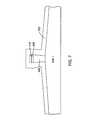
- FIG. 3Bshows an enlarged view of a portion of the write head 306 as viewed from the air bearing surface ABS.
- the write pole 314preferably has a trapezoidal shape as viewed from the air bearing surface (ABS).
- the magnetic shield 338wraps around the sides of the write pole 314 , and is separated from the sides of the write pole 314 by non-magnetic side-gap layers 342 , 344 , which may be constructed of a material such as alumina.
- FIG. 3Cshows a top down, cross sectional view as taken from line 3 C- 3 C of FIG. 3B .
- the write pole 314has a pole tip portion 346 with a relatively constant cross section, and has a flare portion 348 that flares laterally outward.
- the transition point between the pole tip portion 346 and the flared portion 348defines a flare point 349 .
- the side gap layers 342 , 344define a side gap having a width W 1 in the pole tip region.
- an extra layer of non-magnetic side gap material 350 , 352 at each side of the write pole 314provides an increased side gap thickness W 2 in the flared region.
- This increased side gap thickness W 2 in the flared region 348 of the write poleresults in improved magnetic performance and can be created by a novel manufacturing method that will be described herein below.
- the wider side gap thickness W 2improves magnetic performance of the write head by minimizing the loss of write field to the side portions of the shield 338 during writing, thereby ensuring maximum write field.
- a substrate 404is provided.
- the substratecan include the insulation layer 326 and all or a portion of the shaping layer 320 described above with reference to FIG. 3A .
- a magnetic write pole layer 406is deposited over the substrate.
- the magnetic write pole layer 406is preferably a lamination of magnetic layers separated by thin non-magnetic layers.
- a series of mask layers 402is deposited over the write pole layer 406 .
- the mask layerscan include first and second hard mask layers 408 , 410 , an image transfer layer 411 , a third hard mask layer 412 and a photoresist layer 414 .
- First hard mask layer 408can be a material such as alumina.
- the second hard maskis preferably a material that can be removed by reactive ion etching (RIE) such as SiN and is referred to herein as a RIEable hard mask layer 410 .
- the image transfer layer 411can be a polyimide material such as DURAMIDE® or some similar material.
- the third hard maskcan be, for example, SiO 2 .
- the photoresist layer 414photolithographically patterned to define a write pole structure.
- one or more material removal processessuch as reactive ion etching and or ion milling are performed to transfer the image of the patterned photoresist layer 414 onto the underlying mask layers 408 - 412 .
- an ion millingis performed to remove portions of the write pole material 406 that are not protected by the mask layers 402 .
- the ion millingremoves the photoresist layer 414 , third hard mask 412 and a portion of the image transfer layer 411 , leaving the mask layers 402 as shown in FIG. 6 .
- a wet stripping processthen is performed to remove the remaining layer 412 .
- the non-magnetic side gap layer 702can be alumina and can be deposited by a conformal deposition process such as atomic layer deposition (ALD) or chemical vapor deposition (CVD).
- a material removal processsuch as reactive ion milling (RIM) can be performed to preferentially remove horizontally disposed portions of the non-magnetic side gap layer 702 , leaving non-magnetic side walls as shown in FIG. 8 .
- a CMP processcan be used to remove the horizontally disposed portions of the non-magnetic side gap layers 702 .
- Such a methodcould include depositing a fill layer, performing a CMP process and then removing the fill layer by reactive ion etching.
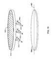
- FIG. 9shows a top down view of the structure as viewed from line 9 - 9 of FIG. 8 .
- the write pole structure 406is hidden beneath the hard mask layer 410 and non-magnetic side walls 702 are formed at the sides of the write pole 406 .
- the non-magnetic side walls 702have a substantially constant cross section at the pole tip and at the flared portion of the write pole 406 .
- a non-magnetic material 1002such as alumina, Ta, TaO, etc. is deposited.
- the non-magnetic material 1002is deposited by a collimated sputtering process that causes the material 1002 to be deposited much more readily on the sides of the flared portion than on the sides of the pole tip portion.
- the collimated sputteringis performed in such a manner as to deposit the non-magnetic material 1002 primarily in a direction perpendicular to an air bearing surface plane (ABS) as indicated by the arrows 1004
- ABSair bearing surface plane
- FIGS. 11 and 12illustrate the results of this collimated sputtering as viewed in cross section from the lines 11 - 11 of FIG. 10 and 12 - 12 of FIG. 10 . Therefore, FIG. 11 shows a cross section of the structure in the constant cross-section, pole tip portion of the write pole 406 and FIG. 12 shows a cross section of the flared portion of the write pole 406 .
- the collimated sputter depositiondeposits the non-magnetic layer 1002 on the top of the write pole 406 and hard mask layers 408 , 410 and on the substrate 404 , but with very little material 1002 being deposited on the sides of the non-magnetic side walls 702 .
- the non-magnetic material 1002is deposited on the sides of the side gap layers 702 as well as on the tops of the write pole 406 and substrate 404 .
- FIGS. 13 and 14A material removal process such as reactive ion etching or ion milling is then performed to preferentially remove horizontally disposed portions of the deposited non-magnetic layer and also to remove the RIEable hard mask layer 410 , leaving a structure such as shown in FIGS. 13 and 14 .
- FIG. 13shows a cross section taken at the pole tip portion, and as can be seen, the non-magnetic layer 1002 ( FIG. 11 ) has essentially been completely removed.
- FIG. 14which shows a cross sectional view at the flared portion of the write pole 406 vertical side walls of the non-magnetic material 1002 remain, thereby creating a wider non-magnetic side wall that is the sum of the side gap layer 702 and layer 1002 .
- FIGS. 15 , 16 and 17a magnetic, electrically conductive seed layer 1502 is deposited and a magnetic shield 1504 is electroplated onto the seed layer 1502 .
- FIG. 15shows a cross section in the pole tip region and
- FIG. 16shows a cross section in the flared region.
- the magnetic shieldhas a wider side gap in the flared region than in the pole tip region due to the presence of the additional non-magnetic side gap layer 1002 .
- the magnetic shield 1504can be electroplated into a photoresist plating frame mask (not shown) to form a trailing shield having front and back edges 1702 , 1704 as shown in FIG. 17 .
- the front and back edges 1702 , 1704can be located on opposite sides of the flare point 1706 .
- An ion millingcan be performed to remove portions of the seed layer 1502 that are not protected by the shield 1504 .
- the sputtering operationis performed in a sputter deposition tool 1802 that includes a chamber 1804 .
- a chuck 1806is mounted within the chamber.
- the chuck 1806supports a wafer 1808 within the chamber 1804 .
- a target 1810is also mounted within the chamber, the target being constructed of a material to be sputter deposited.
- An ion beam gun 1812directs an ion beam 1814 at the target 1810 .
- This ion beam 1814dislodges particles 1816 in the form of atoms and/or ions from the target 1810 which travel toward the wafer 1808 .
- the particles 1816 as they are initially dislodged from the target 1810travel in random directions.
- a collimator 1818is provided within the chamber, the collimator 1818 being located between the target 1810 and the wafer 1808 .
- the collimatoracts to orient the particles along a desired plane, so that particles 1816 being deposited onto the wafer 1808 are deposited primarily along a desired plane.
- FIG. 19shows a perspective view of the wafer 1808 and collimator 1816 .
- the collimator 1818can be configured with slots 1902 that align the particles 1816 in a desired direction.
- the collimator 1902is arranged so as to align the particles 1816 along a plane in a direction 1904 oriented substantially perpendicular to an air bearing surface plane that is oriented as indicated by the line labeled ABS.
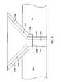
- FIGS. 20 and 21a write head 2002 according to an alternate embodiment of the invention is described.
- This embodimentincludes a stitched magnetic layer 2004 that defines a stitched flare point for more accurate flare point location relative to the ABS.
- the stitched magnetic layer 2002is formed over the write pole 314 , and wraps around the write pole 314 as can be seen more clearly with reference to FIG. 21 which shows a top down sectional view taken from the line 21 - 21 of FIG. 20 .
- the write pole 314has stitched magnetic layer formed thereover.
- the stitched magnetic layerhas a front edge 2102 , located in front of the flare point 2104 , and which defines a stitched flare point.
- a non-magnetic side gap layer 2106is provided at the sides of the write pole 314 in the pole tip region to provide a desired non-magnetic side gap separation between the write pole 314 and the magnetic shield 338 which is not shown in FIG. 21 .
- This magnetic layer 2106is also formed at sides of the stitched pole 2004 , thereby providing a side gap for the stitched magnetic layer 2004 . As can be seen with reference to FIG. 20 , the non-magnetic layer 2106 also provides a separation between the trailing shield 338 and the stitched magnetic layer 2004 .
- the non-magnetic layer 2106provides non-magnetic spacing between the stitched magnetic pole 2004 and the trailing shield 338 both at the sides of the stitched pole 2004 and at the front edge 2102 of the stitched pole 2004 .
- the spacing between the stitched pole 2004 and the shield 338must be much smaller at the front edge 2102 than at the sides of the stitched pole 2004 . Therefore, the non-magnetic layer 2106 is much thinner at the front edge 2102 of the stitched pole 2004 than at the sides of the stitched pole.
- the present inventionprovides a method for constructing such a non-magnetic layer 2004 , which is described below.
- a methodis described for manufacturing a magnetic write head such as that described above.
- a write pole 314is formed, such as by the previously described processes.
- a stitched magnetic pole layer 2004is electroplated over a back portion of the write pole.
- a mask structure(not shown) can be formed over the pole tip region of the write pole so that the electroplated stitched magnetic pole layer 2004 has a desired front edge 2102 .
- the portions of the write pole 314 that are hidden beneath the stitched magnetic pole layer 2004are shown in dotted line.
- a collimated sputtering deposition of a non-magnetic material such as alumina, Ta, TaO, etc. 2106is performed.
- This collimated sputteringis performed in a manner such as described above with reference to FIGS. 18 and 19 , except that the orientation of the collimator 1818 ( FIG. 19 ) is rotated 90 degrees.
- the material 2106is deposited primarily in a plane that is parallel with the ABS plane as indicated by double headed arrow symbol 2302 .
- This collimated sputter deposition of the non-magnetic material 2106causes the non-magnetic material 2106 to be deposited much more readily on the sides of the write pole 314 and stitched pole layer 2004 than on the front surface 2102 . This forms the non-magnetic layer with the desired larger thickness at the sides and smaller thickness at the front edge 2102 as discussed above with reference to FIGS. 20 and 21 .
- a material removal processsuch as ion milling or reactive ion etching can be performed to remove all or a potion of the non-magnetic material from the tops of the write pole 314 and stitched pole layer 2004 as desired.
- a magnetic, trailing, wrap-around shieldcan then be electroplated over the write pole 314 and stitched pole 2004 after an electrically conductive seed-layer is deposited.
Landscapes
- Engineering & Computer Science (AREA)
- Manufacturing & Machinery (AREA)
- Physics & Mathematics (AREA)
- Electromagnetism (AREA)
- Magnetic Heads (AREA)
Abstract
Description
Claims (3)
Priority Applications (1)
| Application Number | Priority Date | Filing Date | Title |
|---|---|---|---|
| US11/966,086US8139320B2 (en) | 2007-12-28 | 2007-12-28 | Write head having independent side shield and trailing shield throat height |
Applications Claiming Priority (1)
| Application Number | Priority Date | Filing Date | Title |
|---|---|---|---|
| US11/966,086US8139320B2 (en) | 2007-12-28 | 2007-12-28 | Write head having independent side shield and trailing shield throat height |
Publications (2)
| Publication Number | Publication Date |
|---|---|
| US20090168257A1 US20090168257A1 (en) | 2009-07-02 |
| US8139320B2true US8139320B2 (en) | 2012-03-20 |
Family
ID=40797983
Family Applications (1)
| Application Number | Title | Priority Date | Filing Date |
|---|---|---|---|
| US11/966,086Active2030-10-18US8139320B2 (en) | 2007-12-28 | 2007-12-28 | Write head having independent side shield and trailing shield throat height |
Country Status (1)
| Country | Link |
|---|---|
| US (1) | US8139320B2 (en) |
Cited By (8)
| Publication number | Priority date | Publication date | Assignee | Title |
|---|---|---|---|---|
| US20120107645A1 (en)* | 2007-11-02 | 2012-05-03 | Hitachi Global Storage Technologies Netherlands B.V. | Method for manufacturing a short flare definition by additive process for perpendicular head |
| US8488272B1 (en) | 2008-08-27 | 2013-07-16 | Western Digital (Fremont), Llc | Magnetic recording transducer having side shields |
| US8533937B1 (en)* | 2011-10-18 | 2013-09-17 | Western Digital (Fremont), Llc | Method of forming a fully wrapped-around shielded PMR writer pole |
| US8576517B1 (en)* | 2008-08-26 | 2013-11-05 | Western Digital (Fremont), Llc | Magnetic recording transducer having side shields between the coils and the air-bearing surface |
| US8720044B1 (en) | 2008-09-26 | 2014-05-13 | Western Digital (Fremont), Llc | Method for manufacturing a magnetic recording transducer having side shields |
| US8801943B2 (en)* | 2011-07-28 | 2014-08-12 | HGST Netherlands B.V. | Method for manufacturing wraparound shield write head using hard masks |
| US9135930B1 (en) | 2014-03-06 | 2015-09-15 | Western Digital (Fremont), Llc | Method for fabricating a magnetic write pole using vacuum deposition |
| US9396741B1 (en) | 2015-08-28 | 2016-07-19 | Seagate Technology Llc | Data writer side shield with cantilevered protrusions |
Families Citing this family (8)
| Publication number | Priority date | Publication date | Assignee | Title |
|---|---|---|---|---|
| US8259413B2 (en)* | 2008-12-31 | 2012-09-04 | Hitachi Global Storage Technologies Netherlands B.V. | Write head with self-align layer and a method for making the same |
| US8634161B2 (en)* | 2008-12-31 | 2014-01-21 | HGST Netherlands, B.V. | Systems having writer with deeper wrap around shield and methods for making the same |
| US8339741B2 (en)* | 2009-06-22 | 2012-12-25 | Seagate Technology Llc | Write pole trailing edge partial side shield |
| US8323727B2 (en)* | 2009-12-17 | 2012-12-04 | Hitachi Global Storage Technologies Netherlands B.V. | Method for manufacturing a perpendicular magnetic write head having a tapered write pole and a stepped wrap around side shield gap |
| US8611046B2 (en)* | 2010-04-19 | 2013-12-17 | Headway Technologies, Inc. | PMR writer with graded side shield |
| US8451562B2 (en) | 2010-04-23 | 2013-05-28 | HGST Netherlands B.V. | Method for manufacturing a magnetic write head having a wrap around trailing magnetic shield with a tapered side gap |
| US8339734B2 (en) | 2010-04-23 | 2012-12-25 | Hitachi Global Storage Technologies Netherlands B.V. | Magnetic write head having a wrap around trailing shield with an asymetrical side gap |
| US8767344B2 (en) | 2010-12-22 | 2014-07-01 | HGST Netherlands B.V. | Magnetic recording head having a non-conformal side gap and methods of production thereof |
Citations (14)
| Publication number | Priority date | Publication date | Assignee | Title |
|---|---|---|---|---|
| US5075956A (en)* | 1988-03-16 | 1991-12-31 | Digital Equipment Corporation | Method of making recording heads with side shields |
| US6305072B1 (en) | 1996-11-28 | 2001-10-23 | Kabushiki Kaisha Toshiba | Method for manufacturing thin film magnetic head |
| US6669855B2 (en) | 2000-01-25 | 2003-12-30 | Tdk Corporation | Method of manufacturing thin film magnetic head |
| US6694604B2 (en) | 1998-04-10 | 2004-02-24 | Hitachi Global Storage Technologies Netherlands B.V. | Method of making a write head with self-aligned pedestal shaped pole tip which are separated by a zero throat height defining layer |
| US6775902B1 (en) | 1997-07-28 | 2004-08-17 | Western Digital (Fremont) Inc. | Method of making a magnetic head with aligned pole tips |
| US20050141137A1 (en)* | 2003-12-24 | 2005-06-30 | Hitachi Global Storage Technologies Netherlands, B.V. | Magnetic recording head for perpendicular recording, fabrication process, and magnetic disk storage apparatus mounting the magnetic head |
| US20050190491A1 (en) | 2004-02-27 | 2005-09-01 | Hitachi Global Storage Technologies | Self-aligned, notched trailing shield for perpendicular recording |
| US6980403B2 (en) | 2002-03-12 | 2005-12-27 | Alps Electric Co., Ltd. | Magnetic sensing element with side shield layers |
| US20060044682A1 (en) | 2004-08-31 | 2006-03-02 | Quang Le | Self aligned wrap around shield for perpendicular magnetic recording |
| US7100266B2 (en) | 2001-05-16 | 2006-09-05 | Seagate Technology Llc | Method of forming a beveled writing pole of a perpendicular writing element |
| US20060198049A1 (en)* | 2005-03-07 | 2006-09-07 | Headway Technologies, Inc. | Magnetic head for perpendicular magnetic recording and method of manufacturing same |
| US20070035878A1 (en) | 2005-08-10 | 2007-02-15 | Hung-Chin Guthrie | Perpendicular head with self-aligned notching trailing shield process |
| US20080259498A1 (en)* | 2007-04-19 | 2008-10-23 | Hitachi Global Storage Technologies | Perpendicular write head with independent trailing shield designs |
| US20090283205A1 (en)* | 2008-05-16 | 2009-11-19 | Fujitsu Limited | Method of manufacturing a thin-film magnetic head |
Family Cites Families (1)
| Publication number | Priority date | Publication date | Assignee | Title |
|---|---|---|---|---|
| US7061728B2 (en)* | 2003-07-29 | 2006-06-13 | Hitachi Global Storage Technologies Netherlands B.V. | High linear density read head with a contiguous junction and minimal shield shorts |
- 2007
- 2007-12-28USUS11/966,086patent/US8139320B2/enactiveActive
Patent Citations (14)
| Publication number | Priority date | Publication date | Assignee | Title |
|---|---|---|---|---|
| US5075956A (en)* | 1988-03-16 | 1991-12-31 | Digital Equipment Corporation | Method of making recording heads with side shields |
| US6305072B1 (en) | 1996-11-28 | 2001-10-23 | Kabushiki Kaisha Toshiba | Method for manufacturing thin film magnetic head |
| US6775902B1 (en) | 1997-07-28 | 2004-08-17 | Western Digital (Fremont) Inc. | Method of making a magnetic head with aligned pole tips |
| US6694604B2 (en) | 1998-04-10 | 2004-02-24 | Hitachi Global Storage Technologies Netherlands B.V. | Method of making a write head with self-aligned pedestal shaped pole tip which are separated by a zero throat height defining layer |
| US6669855B2 (en) | 2000-01-25 | 2003-12-30 | Tdk Corporation | Method of manufacturing thin film magnetic head |
| US7100266B2 (en) | 2001-05-16 | 2006-09-05 | Seagate Technology Llc | Method of forming a beveled writing pole of a perpendicular writing element |
| US6980403B2 (en) | 2002-03-12 | 2005-12-27 | Alps Electric Co., Ltd. | Magnetic sensing element with side shield layers |
| US20050141137A1 (en)* | 2003-12-24 | 2005-06-30 | Hitachi Global Storage Technologies Netherlands, B.V. | Magnetic recording head for perpendicular recording, fabrication process, and magnetic disk storage apparatus mounting the magnetic head |
| US20050190491A1 (en) | 2004-02-27 | 2005-09-01 | Hitachi Global Storage Technologies | Self-aligned, notched trailing shield for perpendicular recording |
| US20060044682A1 (en) | 2004-08-31 | 2006-03-02 | Quang Le | Self aligned wrap around shield for perpendicular magnetic recording |
| US20060198049A1 (en)* | 2005-03-07 | 2006-09-07 | Headway Technologies, Inc. | Magnetic head for perpendicular magnetic recording and method of manufacturing same |
| US20070035878A1 (en) | 2005-08-10 | 2007-02-15 | Hung-Chin Guthrie | Perpendicular head with self-aligned notching trailing shield process |
| US20080259498A1 (en)* | 2007-04-19 | 2008-10-23 | Hitachi Global Storage Technologies | Perpendicular write head with independent trailing shield designs |
| US20090283205A1 (en)* | 2008-05-16 | 2009-11-19 | Fujitsu Limited | Method of manufacturing a thin-film magnetic head |
Cited By (10)
| Publication number | Priority date | Publication date | Assignee | Title |
|---|---|---|---|---|
| US20120107645A1 (en)* | 2007-11-02 | 2012-05-03 | Hitachi Global Storage Technologies Netherlands B.V. | Method for manufacturing a short flare definition by additive process for perpendicular head |
| US8503131B2 (en)* | 2007-11-02 | 2013-08-06 | HGST Netherlands B.V. | Perpendicular magnetic write head having a novel shield structure |
| US8576517B1 (en)* | 2008-08-26 | 2013-11-05 | Western Digital (Fremont), Llc | Magnetic recording transducer having side shields between the coils and the air-bearing surface |
| US8488272B1 (en) | 2008-08-27 | 2013-07-16 | Western Digital (Fremont), Llc | Magnetic recording transducer having side shields |
| US8720044B1 (en) | 2008-09-26 | 2014-05-13 | Western Digital (Fremont), Llc | Method for manufacturing a magnetic recording transducer having side shields |
| US8801943B2 (en)* | 2011-07-28 | 2014-08-12 | HGST Netherlands B.V. | Method for manufacturing wraparound shield write head using hard masks |
| US8533937B1 (en)* | 2011-10-18 | 2013-09-17 | Western Digital (Fremont), Llc | Method of forming a fully wrapped-around shielded PMR writer pole |
| US9520146B1 (en)* | 2011-10-18 | 2016-12-13 | Western Digital (Fremont), Llc | Method of forming a fully wrapped-around shielded PMR writer pole |
| US9135930B1 (en) | 2014-03-06 | 2015-09-15 | Western Digital (Fremont), Llc | Method for fabricating a magnetic write pole using vacuum deposition |
| US9396741B1 (en) | 2015-08-28 | 2016-07-19 | Seagate Technology Llc | Data writer side shield with cantilevered protrusions |
Also Published As
| Publication number | Publication date |
|---|---|
| US20090168257A1 (en) | 2009-07-02 |
Similar Documents
| Publication | Publication Date | Title |
|---|---|---|
| US8139320B2 (en) | Write head having independent side shield and trailing shield throat height | |
| US8323727B2 (en) | Method for manufacturing a perpendicular magnetic write head having a tapered write pole and a stepped wrap around side shield gap | |
| US8066892B2 (en) | Method for manufacturing a perpendicular magnetic write head with a wrap around shield | |
| US8000059B2 (en) | Perpendicular magnetic write head with a thin wrap around magnetic shield | |
| US8068312B2 (en) | Perpendicular magnetic write head with stitched notched trailing shield | |
| US7963024B2 (en) | Method of manufacturing a magnetic write head for perpendicular magnetic recording | |
| US8201320B2 (en) | Method for manufacturing a magnetic write head having a wrap around shield that is magnetically coupled with a leading magnetic shield | |
| US8441757B2 (en) | Perpendicular magnetic write head with wrap-around shield, slanted pole and slanted pole bump fabricated by damascene process | |
| US8347488B2 (en) | Magnetic write head manufactured by damascene process producing a tapered write pole with a non-magnetic step and non-magnetic bump | |
| US8347489B2 (en) | Method for manufacturing a perpendicular magnetic write head having a leading edge tapered write pole, self aligned side shield and independent trailing shield | |
| US8110085B2 (en) | Assisted deposition, narrow trench damascene process for manufacturing a write pole of a magnetic write head | |
| US8339734B2 (en) | Magnetic write head having a wrap around trailing shield with an asymetrical side gap | |
| US8189292B2 (en) | Method for manufacturing a magnetic write head having a write pole with a trailing edge taper using a Rieable hard mask | |
| US7793406B2 (en) | Method for manufacturing a magnetic write head | |
| US8451562B2 (en) | Method for manufacturing a magnetic write head having a wrap around trailing magnetic shield with a tapered side gap | |
| US20100157472A1 (en) | Magnetic write head having a self-aligned side wrap-around shield with multi-angle slanted bump | |
| US8268407B2 (en) | Method for manufacturing a perpendicular magnetic write head having write pole | |
| US7788798B2 (en) | Method for manufacturing a perpendicular magnetic write head with wrap around magnetic trailing and side shields | |
| US7881010B2 (en) | Process for self-aligned flare point and shield throat definition prior to main pole patterning | |
| US20100155364A1 (en) | Magnetic write head having a stepped trailing shield and write pole with a sloped trailing edge | |
| US8349197B2 (en) | Method for manufacturing a perpendicular magnetic write head having a tapered write pole and non-magnetic bump structure | |
| US8514518B2 (en) | Flat E-yoke for cusp write head | |
| US8318031B2 (en) | Method for manufacturing a perpendicular magnetic write head having a tapered write pole | |
| US8252190B2 (en) | Method for manufacturing a magnetic write head having a hard mask defined write pole trailing edge step | |
| US20100155232A1 (en) | Method for manufacturing a magnetic write head having a write pole trailing edge taper |
Legal Events
| Date | Code | Title | Description |
|---|---|---|---|
| AS | Assignment | Owner name:HITACHI GLOBAL STORAGE TECHNOLOGIES NETHERLANDS B. Free format text:ASSIGNMENT OF ASSIGNORS INTEREST;ASSIGNORS:HSIAO, WEN-CHIEN DAVID;LIU, YINSHI;ZHENG, YI;REEL/FRAME:020545/0255 Effective date:20071220 | |
| FEPP | Fee payment procedure | Free format text:PAYOR NUMBER ASSIGNED (ORIGINAL EVENT CODE: ASPN); ENTITY STATUS OF PATENT OWNER: LARGE ENTITY | |
| STCF | Information on status: patent grant | Free format text:PATENTED CASE | |
| AS | Assignment | Owner name:HGST, NETHERLANDS B.V., NETHERLANDS Free format text:CHANGE OF NAME;ASSIGNOR:HGST, NETHERLANDS B.V.;REEL/FRAME:029341/0777 Effective date:20120723 Owner name:HGST NETHERLANDS B.V., NETHERLANDS Free format text:CHANGE OF NAME;ASSIGNOR:HITACHI GLOBAL STORAGE TECHNOLOGIES NETHERLANDS B.V.;REEL/FRAME:029341/0777 Effective date:20120723 | |
| FPAY | Fee payment | Year of fee payment:4 | |
| AS | Assignment | Owner name:WESTERN DIGITAL TECHNOLOGIES, INC., CALIFORNIA Free format text:ASSIGNMENT OF ASSIGNORS INTEREST;ASSIGNOR:HGST NETHERLANDS B.V.;REEL/FRAME:040826/0821 Effective date:20160831 | |
| MAFP | Maintenance fee payment | Free format text:PAYMENT OF MAINTENANCE FEE, 8TH YEAR, LARGE ENTITY (ORIGINAL EVENT CODE: M1552); ENTITY STATUS OF PATENT OWNER: LARGE ENTITY Year of fee payment:8 | |
| AS | Assignment | Owner name:JPMORGAN CHASE BANK, N.A., AS AGENT, ILLINOIS Free format text:SECURITY INTEREST;ASSIGNOR:WESTERN DIGITAL TECHNOLOGIES, INC.;REEL/FRAME:052915/0566 Effective date:20200113 | |
| AS | Assignment | Owner name:WESTERN DIGITAL TECHNOLOGIES, INC., CALIFORNIA Free format text:RELEASE OF SECURITY INTEREST AT REEL 052915 FRAME 0566;ASSIGNOR:JPMORGAN CHASE BANK, N.A.;REEL/FRAME:059127/0001 Effective date:20220203 | |
| AS | Assignment | Owner name:JPMORGAN CHASE BANK, N.A., ILLINOIS Free format text:PATENT COLLATERAL AGREEMENT - A&R LOAN AGREEMENT;ASSIGNOR:WESTERN DIGITAL TECHNOLOGIES, INC.;REEL/FRAME:064715/0001 Effective date:20230818 Owner name:JPMORGAN CHASE BANK, N.A., ILLINOIS Free format text:PATENT COLLATERAL AGREEMENT - DDTL LOAN AGREEMENT;ASSIGNOR:WESTERN DIGITAL TECHNOLOGIES, INC.;REEL/FRAME:067045/0156 Effective date:20230818 | |
| MAFP | Maintenance fee payment | Free format text:PAYMENT OF MAINTENANCE FEE, 12TH YEAR, LARGE ENTITY (ORIGINAL EVENT CODE: M1553); ENTITY STATUS OF PATENT OWNER: LARGE ENTITY Year of fee payment:12 |