US8139002B2 - Organic light emitting diode display and driving method thereof - Google Patents
Organic light emitting diode display and driving method thereofDownload PDFInfo
- Publication number
- US8139002B2 US8139002B2US11/819,276US81927607AUS8139002B2US 8139002 B2US8139002 B2US 8139002B2US 81927607 AUS81927607 AUS 81927607AUS 8139002 B2US8139002 B2US 8139002B2
- Authority
- US
- United States
- Prior art keywords
- voltage
- light emitting
- emitting diode
- organic light
- horizontal period
- Prior art date
- Legal status (The legal status is an assumption and is not a legal conclusion. Google has not performed a legal analysis and makes no representation as to the accuracy of the status listed.)
- Active, expires
Links
Images


Classifications
- G—PHYSICS
- G09—EDUCATION; CRYPTOGRAPHY; DISPLAY; ADVERTISING; SEALS
- G09G—ARRANGEMENTS OR CIRCUITS FOR CONTROL OF INDICATING DEVICES USING STATIC MEANS TO PRESENT VARIABLE INFORMATION
- G09G3/00—Control arrangements or circuits, of interest only in connection with visual indicators other than cathode-ray tubes
- G09G3/20—Control arrangements or circuits, of interest only in connection with visual indicators other than cathode-ray tubes for presentation of an assembly of a number of characters, e.g. a page, by composing the assembly by combination of individual elements arranged in a matrix no fixed position being assigned to or needed to be assigned to the individual characters or partial characters
- G09G3/22—Control arrangements or circuits, of interest only in connection with visual indicators other than cathode-ray tubes for presentation of an assembly of a number of characters, e.g. a page, by composing the assembly by combination of individual elements arranged in a matrix no fixed position being assigned to or needed to be assigned to the individual characters or partial characters using controlled light sources
- G09G3/30—Control arrangements or circuits, of interest only in connection with visual indicators other than cathode-ray tubes for presentation of an assembly of a number of characters, e.g. a page, by composing the assembly by combination of individual elements arranged in a matrix no fixed position being assigned to or needed to be assigned to the individual characters or partial characters using controlled light sources using electroluminescent panels
- G09G3/32—Control arrangements or circuits, of interest only in connection with visual indicators other than cathode-ray tubes for presentation of an assembly of a number of characters, e.g. a page, by composing the assembly by combination of individual elements arranged in a matrix no fixed position being assigned to or needed to be assigned to the individual characters or partial characters using controlled light sources using electroluminescent panels semiconductive, e.g. using light-emitting diodes [LED]
- G09G3/3208—Control arrangements or circuits, of interest only in connection with visual indicators other than cathode-ray tubes for presentation of an assembly of a number of characters, e.g. a page, by composing the assembly by combination of individual elements arranged in a matrix no fixed position being assigned to or needed to be assigned to the individual characters or partial characters using controlled light sources using electroluminescent panels semiconductive, e.g. using light-emitting diodes [LED] organic, e.g. using organic light-emitting diodes [OLED]
- G—PHYSICS
- G09—EDUCATION; CRYPTOGRAPHY; DISPLAY; ADVERTISING; SEALS
- G09G—ARRANGEMENTS OR CIRCUITS FOR CONTROL OF INDICATING DEVICES USING STATIC MEANS TO PRESENT VARIABLE INFORMATION
- G09G3/00—Control arrangements or circuits, of interest only in connection with visual indicators other than cathode-ray tubes
- G09G3/20—Control arrangements or circuits, of interest only in connection with visual indicators other than cathode-ray tubes for presentation of an assembly of a number of characters, e.g. a page, by composing the assembly by combination of individual elements arranged in a matrix no fixed position being assigned to or needed to be assigned to the individual characters or partial characters
- G09G3/22—Control arrangements or circuits, of interest only in connection with visual indicators other than cathode-ray tubes for presentation of an assembly of a number of characters, e.g. a page, by composing the assembly by combination of individual elements arranged in a matrix no fixed position being assigned to or needed to be assigned to the individual characters or partial characters using controlled light sources
- G09G3/30—Control arrangements or circuits, of interest only in connection with visual indicators other than cathode-ray tubes for presentation of an assembly of a number of characters, e.g. a page, by composing the assembly by combination of individual elements arranged in a matrix no fixed position being assigned to or needed to be assigned to the individual characters or partial characters using controlled light sources using electroluminescent panels
- G09G3/32—Control arrangements or circuits, of interest only in connection with visual indicators other than cathode-ray tubes for presentation of an assembly of a number of characters, e.g. a page, by composing the assembly by combination of individual elements arranged in a matrix no fixed position being assigned to or needed to be assigned to the individual characters or partial characters using controlled light sources using electroluminescent panels semiconductive, e.g. using light-emitting diodes [LED]
- G09G3/3208—Control arrangements or circuits, of interest only in connection with visual indicators other than cathode-ray tubes for presentation of an assembly of a number of characters, e.g. a page, by composing the assembly by combination of individual elements arranged in a matrix no fixed position being assigned to or needed to be assigned to the individual characters or partial characters using controlled light sources using electroluminescent panels semiconductive, e.g. using light-emitting diodes [LED] organic, e.g. using organic light-emitting diodes [OLED]
- G09G3/3225—Control arrangements or circuits, of interest only in connection with visual indicators other than cathode-ray tubes for presentation of an assembly of a number of characters, e.g. a page, by composing the assembly by combination of individual elements arranged in a matrix no fixed position being assigned to or needed to be assigned to the individual characters or partial characters using controlled light sources using electroluminescent panels semiconductive, e.g. using light-emitting diodes [LED] organic, e.g. using organic light-emitting diodes [OLED] using an active matrix
- G—PHYSICS
- G09—EDUCATION; CRYPTOGRAPHY; DISPLAY; ADVERTISING; SEALS
- G09G—ARRANGEMENTS OR CIRCUITS FOR CONTROL OF INDICATING DEVICES USING STATIC MEANS TO PRESENT VARIABLE INFORMATION
- G09G2310/00—Command of the display device
- G09G2310/02—Addressing, scanning or driving the display screen or processing steps related thereto
- G09G2310/0243—Details of the generation of driving signals
- G09G2310/0245—Clearing or presetting the whole screen independently of waveforms, e.g. on power-on
- G—PHYSICS
- G09—EDUCATION; CRYPTOGRAPHY; DISPLAY; ADVERTISING; SEALS
- G09G—ARRANGEMENTS OR CIRCUITS FOR CONTROL OF INDICATING DEVICES USING STATIC MEANS TO PRESENT VARIABLE INFORMATION
- G09G2310/00—Command of the display device
- G09G2310/02—Addressing, scanning or driving the display screen or processing steps related thereto
- G09G2310/0243—Details of the generation of driving signals
- G09G2310/0251—Precharge or discharge of pixel before applying new pixel voltage
- G—PHYSICS
- G09—EDUCATION; CRYPTOGRAPHY; DISPLAY; ADVERTISING; SEALS
- G09G—ARRANGEMENTS OR CIRCUITS FOR CONTROL OF INDICATING DEVICES USING STATIC MEANS TO PRESENT VARIABLE INFORMATION
- G09G2320/00—Control of display operating conditions
- G09G2320/02—Improving the quality of display appearance
- G09G2320/0219—Reducing feedthrough effects in active matrix panels, i.e. voltage changes on the scan electrode influencing the pixel voltage due to capacitive coupling
- G—PHYSICS
- G09—EDUCATION; CRYPTOGRAPHY; DISPLAY; ADVERTISING; SEALS
- G09G—ARRANGEMENTS OR CIRCUITS FOR CONTROL OF INDICATING DEVICES USING STATIC MEANS TO PRESENT VARIABLE INFORMATION
- G09G2320/00—Control of display operating conditions
- G09G2320/02—Improving the quality of display appearance
- G09G2320/0233—Improving the luminance or brightness uniformity across the screen
- G—PHYSICS
- G09—EDUCATION; CRYPTOGRAPHY; DISPLAY; ADVERTISING; SEALS
- G09G—ARRANGEMENTS OR CIRCUITS FOR CONTROL OF INDICATING DEVICES USING STATIC MEANS TO PRESENT VARIABLE INFORMATION
- G09G2320/00—Control of display operating conditions
- G09G2320/02—Improving the quality of display appearance
- G09G2320/0257—Reduction of after-image effects
- G—PHYSICS
- G09—EDUCATION; CRYPTOGRAPHY; DISPLAY; ADVERTISING; SEALS
- G09G—ARRANGEMENTS OR CIRCUITS FOR CONTROL OF INDICATING DEVICES USING STATIC MEANS TO PRESENT VARIABLE INFORMATION
- G09G3/00—Control arrangements or circuits, of interest only in connection with visual indicators other than cathode-ray tubes
- G09G3/20—Control arrangements or circuits, of interest only in connection with visual indicators other than cathode-ray tubes for presentation of an assembly of a number of characters, e.g. a page, by composing the assembly by combination of individual elements arranged in a matrix no fixed position being assigned to or needed to be assigned to the individual characters or partial characters
- G09G3/2092—Details of a display terminals using a flat panel, the details relating to the control arrangement of the display terminal and to the interfaces thereto
- G09G3/2096—Details of the interface to the display terminal specific for a flat panel
- G—PHYSICS
- G09—EDUCATION; CRYPTOGRAPHY; DISPLAY; ADVERTISING; SEALS
- G09G—ARRANGEMENTS OR CIRCUITS FOR CONTROL OF INDICATING DEVICES USING STATIC MEANS TO PRESENT VARIABLE INFORMATION
- G09G3/00—Control arrangements or circuits, of interest only in connection with visual indicators other than cathode-ray tubes
- G09G3/20—Control arrangements or circuits, of interest only in connection with visual indicators other than cathode-ray tubes for presentation of an assembly of a number of characters, e.g. a page, by composing the assembly by combination of individual elements arranged in a matrix no fixed position being assigned to or needed to be assigned to the individual characters or partial characters
- G09G3/22—Control arrangements or circuits, of interest only in connection with visual indicators other than cathode-ray tubes for presentation of an assembly of a number of characters, e.g. a page, by composing the assembly by combination of individual elements arranged in a matrix no fixed position being assigned to or needed to be assigned to the individual characters or partial characters using controlled light sources
- G09G3/30—Control arrangements or circuits, of interest only in connection with visual indicators other than cathode-ray tubes for presentation of an assembly of a number of characters, e.g. a page, by composing the assembly by combination of individual elements arranged in a matrix no fixed position being assigned to or needed to be assigned to the individual characters or partial characters using controlled light sources using electroluminescent panels
- G09G3/32—Control arrangements or circuits, of interest only in connection with visual indicators other than cathode-ray tubes for presentation of an assembly of a number of characters, e.g. a page, by composing the assembly by combination of individual elements arranged in a matrix no fixed position being assigned to or needed to be assigned to the individual characters or partial characters using controlled light sources using electroluminescent panels semiconductive, e.g. using light-emitting diodes [LED]
- G09G3/3208—Control arrangements or circuits, of interest only in connection with visual indicators other than cathode-ray tubes for presentation of an assembly of a number of characters, e.g. a page, by composing the assembly by combination of individual elements arranged in a matrix no fixed position being assigned to or needed to be assigned to the individual characters or partial characters using controlled light sources using electroluminescent panels semiconductive, e.g. using light-emitting diodes [LED] organic, e.g. using organic light-emitting diodes [OLED]
- G09G3/3275—Details of drivers for data electrodes
- G09G3/3291—Details of drivers for data electrodes in which the data driver supplies a variable data voltage for setting the current through, or the voltage across, the light-emitting elements
Definitions
- the present inventionrelates to an organic light emitting diode display, and more particularly to an organic light emitting diode display that is adaptive for removing a voltage which is charged into a gate electrode of a driving transistor before a current frame is changed to a next frame, and a driving method thereof.
- Such flat panel display devicesinclude a liquid crystal display (hereinafter, referred to as “LCD”), a field emission display (hereinafter, referred to as “FED”), a plasma display panel (hereinafter, referred to as “PDP”), and an electro-luminescence (hereinafter, referred to as “EL) display device, etc.
- LCDliquid crystal display
- FEDfield emission display
- PDPplasma display panel
- ELelectro-luminescence
- the EL display device among the flat panel display devicesis a self-luminous device which radiates a fluorescent material by a re-combination of an electron and a hole.
- the EL display deviceis largely classified into an inorganic EL display device which uses an inorganic compound and an organic EL display device which uses an organic compound depending upon the fluorescent material. Since such an EL display device has been highlighted as a post-generation display owing to its advantage of a low voltage driving, a self-luminous, a thin profile, a wide viewing angle, a fast response speed, and a high contrast, etc.
- the organic EL display deviceis comprised of an electron injection layer, an electron transport layer, a light emitting layer, a hole transport layer, and a hole injection layer.
- the electron injection layeris disposed between a cathode and an anode.
- a predetermined voltageis applied between an anode and a cathode, an electron which is generated from a cathode moves toward a light emitting layer via the electron injection layer and the electron transport layer, and a hole which is generated from an anode moves toward a light emitting layer via the hole injection layer and the hole transport layer.
- an electron and a hole which are supplied from the electron transport layer and the hole transport layerare re-combined to generate a light in the organic light emitting layer.
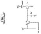
- FIG. 1is an equivalent circuit diagram showing a pixel which is included in an organic light emitting diode display of the related art.
- each pixel of the organic light emitting diode displayincludes a switch transistor S_TR 1 , a storage capacitor Cst, an organic light emitting diode OLED, and a driving transistor D_TR 1 .
- the switch transistor S_TR 1is turned-on by a scanning pulse which is supplied via a gate line GL to switch a data voltage which is supplied via a data line DL.
- the storage capacitor Cstcharges a data voltage which is supplied via the switch transistor S_TR 1 .
- the organic light emitting diode OLEDis turned-on by a driving current which is supplied from a power terminal to which a high potential power voltage VDD is applied to be radiated.
- the driving transistor D_TR 1is turned-on by a data voltage which is supplied via the switch transistor S_TR 1 or a charged voltage of the storage capacitor Cst to drive the organic light emitting diode OLED.
- the switch transistor S_TR 1is a NMOS transistor having a gate electrode, a drain electrode, and a source electrode.
- the gate electrodeis connected to the gate line GL.
- the drain electrodeis connected to the data line DL.
- the source electrodeis commonly connected to the storage capacitor Cst and the gate electrode of the driving transistor D_TR 1 .
- the switch transistor S_TRLis turned-on by a scanning pulse which is supplied via the gate line GL to supply a data voltage which is supplied via the data line DL to the storage capacitor Cst and the driving transistor D_TR 1 .
- One side of the storage capacitor Cstis commonly connected to the switch transistor S_TR 1 and a gate electrode of the driving transistor D_TR 1 , and the other side of the storage capacitor Cst is connected to a ground.
- the storage capacitor Cstis charged by a data voltage which is supplied via the switch transistor S_TR 1 .
- the storage capacitor Cstdischarges a discharge voltage thereof to hold a gate voltage of the driving transistor D_TR 1 from a point that a data voltage, which is supplied via the switch transistor S_TR 1 , is not applied to a gate electrode of the driving transistor D_TR 1 .
- the driving transistor D_TR 1is maintained as a turned-on state by a discharge voltage of the storage capacitor Cst for a holding period when is hold by the storage capacitor Cst.
- a point that a data voltage, which is supplied via the switch transistor S_TR 1 , is not applied to a gate electrode of the driving transistor D_TR 1is a point that a gate voltage of the driving transistor D_TR 1 is dropped.
- the organic light emitting diode OLEDhas an anode and a cathode.
- the anodeis connected to a power terminal to which a high potential power voltage VDD is applied.
- the cathodeis connected to a drain electrode of the driving transistor D_TR 1 .
- the driving transistor D_TR 1is a NMOS transistor having a gate electrode, a drain electrode, and a source electrode.
- the gate electrodeis commonly connected to a source electrode of the switch transistor S_TR 1 and the switch transistor S_TR 1 .
- the drain electrodeis connected to a cathode of the organic light emitting diode OLED.
- the source electrodeis connected to a ground.
- the driving transistor D_TR 1is turned-on by a data voltage which is supplied to a gate electrode via the switch transistor S_TR 1 or a discharge voltage of the switch transistor S-TR 1 which is supplied to a gate electrode to switch a driving current which is flowed into the organic light emitting diode OLED to a ground.
- a driving current which is flowed into the organic light emitting diode OLEDis switched to a ground, so that the organic light emitting diode OLED is radiated by a driving current which is generated by a high potential power voltage VDD.
- the driving transistor D_TR 1is changed to a turned-off state from a state in which the driving transistor D_TR 1 is turned-on by a DC voltage applied to a gate electrode, a gate discharge voltage is maintained.
- the driving transistor D_TR 1is degradated.
- the present inventionis to solve the above-mentioned problem. Accordingly, it is an object of the present invention to provide an organic light emitting diode display that is adaptive for removing a voltage which is charged into a gate electrode of a driving transistor before a current frame is changed to a next frame, and a driving method thereof.
- an organic light emitting diode displaycomprises a display panel having a plurality of pixels that include an organic light emitting diode; a timing controller controlling a driving timing of the inputted video data and controlling a supply timing of a refresh voltage; a data driver converting a digital data which is outputted from the timing controller for a current frame into an analog data voltage to supply it to the pixels, and then supplying the refresh voltage to pixels which are selected among the pixels in accordance with a control of the timing controller; and a gate driver primarily supplying a scanning pulse for a first horizontal period of a current frame to select the pixels to be supplied with a data, and then secondarily supplying a scanning pulse for a second horizontal period of a current frame to select pixels to be supplied with the refresh voltage among the pixels in accordance with a control of the timing controller.
- the refresh voltageis a voltage of 0V.
- the refresh voltageis a negative polarity voltage.
- the timing controllergenerates the refresh voltage to apply it to the data driver.
- the organic light emitting diode display of the present inventionfurther includes a refresh voltage generator to which a power voltage is applied to generate the refresh voltage.
- the timing controllersupplies a mask signal to the gate driver to adjust the first horizontal period and the second horizontal period.
- the first horizontal period and the second horizontal periodare a half horizontal period, respectively.
- the first horizontal periodis different from the second horizontal period.
- the gate driversupplies a scanning pulse for the second horizontal period to select all pixels which are formed at the display panel.
- the gate driverdoes not supply a scanning pulse for the second horizontal period to at least one pixel among pixels which are formed at the display panel.
- a method of driving an organic light emitting diode displayincluding a display panel having a plurality of pixels that include an organic light emitting diode, the method comprises generating a refresh voltage; primarily supplying a scanning pulse for a first horizontal period for a current frame to select the pixels to be supplied with a data; converting a digital data which is inputted for the current frame into an analog data voltage to supply it to pixels which are selected by a scanning pulse for the first horizontal period; secondarily supplying a scanning pulse for a second horizontal period of the current frame to select pixels to be supplied with the refresh voltage among the pixels; and supplying the refresh voltage to pixels which are selected by a scanning pulse for the second horizontal period of the current frame.
- the refresh voltageis a voltage of 0V.
- the refresh voltageis a negative polarity voltage.
- the first horizontal period and the second horizontal periodare a half horizontal period, respectively.
- the first horizontal periodis different from the second horizontal period.
- all pixels which are formed at the display panelare selected by supplying a scanning pulse for the second horizontal period in the step of selecting pixels to be supplied with the refresh voltage.
- a scanning pulseis not supplied to at least one pixel among pixels which are formed at the display panel for the second horizontal period in the step of selecting pixels to be supplied with the refresh voltage.
- FIG. 1is an equivalent circuit diagram showing a pixel which is included in an organic light emitting diode display of the related art
- FIG. 2is a diagram showing a configuration of an organic light emitting diode display according to an embodiment of the present invention
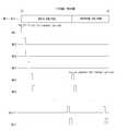
- FIG. 3is a diagram showing an operating characteristics of the organic light emitting diode display according to the present invention.
- FIG. 4is a diagram showing a gray scale characteristics of the organic light emitting diode display according to the present invention.
- FIG. 2is a diagram showing a configuration of an organic light emitting diode display according to an embodiment of the present invention.
- an organic light emitting diode display 100 of the present inventionincludes a display panel 110 , a refresh voltage generator 120 , a timing controller 130 , a data driver 140 , and a gate driver 150 .
- the refresh voltage generator 120is applied with a power voltage to generate a refresh voltage for removing a gate discharge voltage of the driving transistor D_TR 1 .
- the timing controller 130controls a driving timing of a video data which is inputted with a system and, at the same time controls a supply timing of a refresh voltage.
- the data driver 140converts a digital data which is inputted from the timing controller 130 for a current frame into an analog data voltage to supply it to pixels of the display panel 110 , and then supply a refresh voltage from the refresh voltage generator 120 to pixels of the display panel 110 in accordance with a data driving control signal DDC from the timing controller 130 .
- the gate driver 150sequentially supplies a scanning pulse for a half horizontal period to the gate lines GL 1 to GLn for a current frame, and then sequentially supplies a scanning pulse for a half horizontal period to the gate lines GL 5 to GLn in accordance with a gate driving control signal from the timing controller 130 .
- a plurality of data lines DL 1 to DLm and a plurality of gate lines GL 1 to GLnare crossed to be vertical to each other.
- a pixel that includes the organic light emitting diode OLEDis formed at a crossing part thereof.
- An equivalent circuit in FIG. 1is formed at a pixel.
- the refresh voltage generator 120is applied with a power voltage to generate a refresh voltage for removing a gate discharge voltage of the driving transistor D_TR 1 , thereby supplying it to the data driver 140 .
- the refresh voltage generator 120supplies a refresh voltage of 0V or a refresh voltage of negative polarity. This is because only DC voltage of positive polarity is supplied to a gate electrode of the driving transistor D_TR 1 , a refresh voltage of 0V or a refresh voltage of negative polarity is supplied to the driving transistor D_TR 1 to remove a gate discharge voltage of the driving transistor D_TR 1 .
- the refresh voltage generator 120generates a refresh voltage.
- the timing controller 130may generate a refresh voltage to supply it to the data driver 140 .
- the timing controller 130is inputted with a video data from a system such as a TV set or a computer monitor, etc., to supply a digital data to the data driver 140 and, at the same time control a driving of the data.
- the timing controller 130generates a data driving control signal DDC, a refresh control signal RCS, a gate driving control signal GDC, and a mask signal MKS using a horizontal/vertical synchronizing signals H and V from a system in accordance with a clock signal CLK from a system.
- the data driving control signal DDC and the refresh control signal RCSare supplied to the data driver 140 .
- the gate driving control signal GDC and the mask signal MKSare supplied to the gate driver 150 .
- the data driving control signal DDCincludes a source shift clock SSC, a source start pulse SSP, and a source output enable signal SOE, etc.
- the gate driving control signal GDCincludes a gate start pulse GSP and a gate output enable signal GOE, etc.
- the refresh control signal RCScontrols a supply timing of a refresh voltage of the data driver 140 .
- the mask signal MKScontrols a horizontal period of a scanning pulse.
- the data driver 140converts a digital data which is inputted from the timing controller 130 into an analog data voltage in response to a data driving control signal DDC which is supplied from the timing controller 130 to supply it to pixels of the display panel 110 .
- the data driver 140converts a digital data which is supplied via the timing controller 130 into an analog data voltage on the basis of a gamma reference voltage which is supplied from a gamma reference voltage generator 160 to supply it to the data lines DL 1 to DLm.
- an analog data voltageis realized as a gray scale at the organic light emitting diode OLED of the display panel 110 .
- the data driver 140supplies a data at a current frame, and then supplies a refresh voltage to pixels which are selected among the pixels of the display panel 110 for a current frame in accordance with a refresh control signal RCS from the timing controller 130 .
- the data driver 130supplies a data to pixels which are selected by a scanning pulse.
- the scanning pulseis sequentially supplied to the gate lines GL 1 to GLn from the gate driver 150 for a half horizontal period of a current frame.
- the data driver 130supplies a refresh voltage to pixels which are selected by a scanning pulse.
- the scanning pulseis sequentially supplied to the gate lines GL 5 to GLn from the gate driver 150 for a half horizontal period of a current frame.
- the supplied refresh voltageis supplied to a gate electrode of the driving transistor D_TR 1 to remove a gate discharge voltage of a current frame. Accordingly, the present invention can prevent a degradation of the driving transistor and, at the same time remove a residual image of a screen.
- the gate driver 150sequentially supplies a scanning pulse for supplying a data to the gate lines GL 1 to GLn for a current frame, and then sequentially supplies a scanning pulse for refreshing to the gate lines GL 5 to GLn for a current frame in response to a gate driving control signal GDC and a gate shift clock GSC which are supplied from the timing controller 130 as shown in FIG. 3 .
- the gate driver 150sequentially supplies a scanning pulse for the first horizontal period of a half horizontal period, and then sequentially supplies a scanning pulse for the second horizontal period of a half horizontal period in accordance with a mask signal MKS from the timing controller 130 .
- the gate driver 150selects a pixel to be supplied with a data by supplying a scanning pulse for a half horizontal period and, at the same time selects a pixel to be supplied with a refresh voltage by supplying a scanning pulse for a half horizontal period in accordance with a mask signal MKS.
- a period of a scanning pulseis not limited to this.
- the gate driver 150may select a pixel to be supplied with a data by supplying a scanning pulse for a two thirds horizontal period and, at the same time may select a pixel to be supplied with a refresh voltage by supplying a scanning pulse for a one third horizontal period in accordance with a mask signal MKS.
- a scanning pulse for refreshingis supplied to only gate lines GL 5 to GLn.
- a scanning pulse for refreshingmay be sequentially supplied to all gate lines GL 1 to GLn.
- the present inventionsupplies a data voltage, and then supplies a refresh voltage for one frame to remove a gate discharge voltage of the driving transistor.
- the present inventioncan prevent a degradation of the driving transistor and remove a residual image of a screen.
Landscapes
- Engineering & Computer Science (AREA)
- Physics & Mathematics (AREA)
- Computer Hardware Design (AREA)
- General Physics & Mathematics (AREA)
- Theoretical Computer Science (AREA)
- Control Of El Displays (AREA)
- Control Of Indicators Other Than Cathode Ray Tubes (AREA)
- Electroluminescent Light Sources (AREA)
Abstract
Description
Claims (11)
Applications Claiming Priority (3)
| Application Number | Priority Date | Filing Date | Title |
|---|---|---|---|
| KR10-2006-0060760 | 2006-06-30 | ||
| KRP2006-060760 | 2006-06-30 | ||
| KR1020060060760AKR101310912B1 (en) | 2006-06-30 | 2006-06-30 | OLED display and drive method thereof |
Publications (2)
| Publication Number | Publication Date |
|---|---|
| US20080001863A1 US20080001863A1 (en) | 2008-01-03 |
| US8139002B2true US8139002B2 (en) | 2012-03-20 |
Family
ID=38319031
Family Applications (1)
| Application Number | Title | Priority Date | Filing Date |
|---|---|---|---|
| US11/819,276Active2029-08-25US8139002B2 (en) | 2006-06-30 | 2007-06-26 | Organic light emitting diode display and driving method thereof |
Country Status (8)
| Country | Link |
|---|---|
| US (1) | US8139002B2 (en) |
| JP (1) | JP5408847B2 (en) |
| KR (1) | KR101310912B1 (en) |
| CN (1) | CN100555386C (en) |
| DE (1) | DE102007029832B4 (en) |
| FR (1) | FR2904460B1 (en) |
| GB (1) | GB2439801B (en) |
| TW (1) | TWI376664B (en) |
Cited By (2)
| Publication number | Priority date | Publication date | Assignee | Title |
|---|---|---|---|---|
| US20100253664A1 (en)* | 2009-02-20 | 2010-10-07 | Seungchan Byun | Organic light emitting diode display and driving method thereof |
| US9806098B2 (en) | 2013-12-10 | 2017-10-31 | Semiconductor Energy Laboratory Co., Ltd. | Light-emitting device |
Families Citing this family (13)
| Publication number | Priority date | Publication date | Assignee | Title |
|---|---|---|---|---|
| TWI410166B (en)* | 2010-07-19 | 2013-09-21 | Raffar Technology Corp | Gradually refresh control cirtuit of light-emitting unit and method thereof |
| KR101420472B1 (en) | 2010-12-01 | 2014-07-16 | 엘지디스플레이 주식회사 | Organic light emitting diode display device and drving method thereof |
| KR20210078571A (en)* | 2012-03-13 | 2021-06-28 | 가부시키가이샤 한도오따이 에네루기 켄큐쇼 | Light-emitting device and method for driving the same |
| US10235935B2 (en)* | 2013-10-30 | 2019-03-19 | Joled Inc. | Power off method of display device, and display device |
| CN103745685B (en)* | 2013-11-29 | 2015-11-04 | 深圳市华星光电技术有限公司 | Active matric organic LED panel driving circuit and driving method |
| US9653029B2 (en)* | 2014-08-05 | 2017-05-16 | Apple Inc. | Concurrently refreshing multiple areas of a display device using multiple different refresh rates |
| US9779664B2 (en) | 2014-08-05 | 2017-10-03 | Apple Inc. | Concurrently refreshing multiple areas of a display device using multiple different refresh rates |
| KR102127970B1 (en)* | 2014-11-03 | 2020-06-29 | 삼성전자주식회사 | Display apparatus and controlling method thereof |
| KR102360015B1 (en)* | 2015-07-27 | 2022-02-10 | 삼성디스플레이 주식회사 | Pixel, organic light emitting display device including the pixel and driving method of organic light emitting display device |
| KR102478669B1 (en)* | 2015-11-26 | 2022-12-19 | 엘지디스플레이 주식회사 | Organic Light Emitting Display Device and Method of Driving the same |
| KR102546774B1 (en)* | 2016-07-22 | 2023-06-23 | 삼성디스플레이 주식회사 | Display apparatus and method of operating the same |
| CN112382234B (en)* | 2020-11-26 | 2021-11-16 | 昆山国显光电有限公司 | Data calling method of display module and display module |
| CN116364032B (en)* | 2023-03-27 | 2025-09-09 | 惠科股份有限公司 | Display panel driving method and display panel |
Citations (22)
| Publication number | Priority date | Publication date | Assignee | Title |
|---|---|---|---|---|
| US4652872A (en) | 1983-07-07 | 1987-03-24 | Nec Kansai, Ltd. | Matrix display panel driving system |
| US4691144A (en)* | 1986-01-22 | 1987-09-01 | Planar Systems, Inc. | Staggered refresh pulse generator for a TFEL panel |
| US4975691A (en)* | 1987-06-16 | 1990-12-04 | Interstate Electronics Corporation | Scan inversion symmetric drive |
| US5786797A (en)* | 1992-12-10 | 1998-07-28 | Northrop Grumman Corporation | Increased brightness drive system for an electroluminescent display panel |
| US6023259A (en)* | 1997-07-11 | 2000-02-08 | Fed Corporation | OLED active matrix using a single transistor current mode pixel design |
| JP2001164360A (en)* | 1999-12-03 | 2001-06-19 | Matsushita Electronics Industry Corp | Dc sputtering system |
| US20020044109A1 (en)* | 2000-09-29 | 2002-04-18 | Seiko Epson Corporation | Driving method for electro-optical device, electro-optical device, and electronic apparatus |
| US20030193499A1 (en)* | 2002-04-16 | 2003-10-16 | Bo Gao | Object-oriented three-dimensional polygons for the surface modeling of civil engineering objects |
| US20030193490A1 (en)* | 2002-04-11 | 2003-10-16 | Biing-Der Liu | Display driving circuit |
| US20040124780A1 (en)* | 2002-12-27 | 2004-07-01 | Ha Yong Min | Electro-luminescence display device and driving method thereof |
| US20040256617A1 (en)* | 2002-08-26 | 2004-12-23 | Hiroyasu Yamada | Display device and display device driving method |
| US20040263440A1 (en)* | 2003-05-16 | 2004-12-30 | Semiconductor Energy Laboratory Co., Ltd. | Display device and driving method thereof |
| WO2005034072A1 (en)* | 2003-10-02 | 2005-04-14 | Pioneer Corporation | Display apparatus having active matrix display panel, and method for driving the same |
| US20060038758A1 (en)* | 2002-06-18 | 2006-02-23 | Routley Paul R | Display driver circuits |
| US20060044301A1 (en)* | 2004-09-02 | 2006-03-02 | Samsung Electronics Co., Ltd. | Display device and driving method thereof |
| US20060066536A1 (en)* | 2003-05-13 | 2006-03-30 | Masuyuki Ota | Active matrix display device |
| US20060158396A1 (en)* | 2005-01-17 | 2006-07-20 | Seiko Epson Corporation | Electro-optical device, drive circuit, driving method, and electronic apparatus |
| US20060238475A1 (en)* | 2003-12-29 | 2006-10-26 | Lg.Philips Lcd Co. Ltd. | Organic electroluminescent display device and driving method thereof |
| US20060244689A1 (en)* | 2005-04-19 | 2006-11-02 | Semiconductor Energy Laboratory Co., Ltd. | Semiconductor device, display device and electronic apparatus |
| US20070040785A1 (en)* | 2003-04-09 | 2007-02-22 | Koninklijke Philips Electroincs N.V. | Active matrix array device, electronic device and operating method for an active matrix array device |
| US7187373B2 (en)* | 2002-10-11 | 2007-03-06 | Mitsubishi Denki Kabushiki Kaisha | Display apparatus |
| US20070216315A1 (en)* | 2004-06-30 | 2007-09-20 | Eastman Kodak Company | Active matrix display device |
Family Cites Families (1)
| Publication number | Priority date | Publication date | Assignee | Title |
|---|---|---|---|---|
| JP4337327B2 (en)* | 2002-10-31 | 2009-09-30 | セイコーエプソン株式会社 | Display and electronic equipment |
- 2006
- 2006-06-30KRKR1020060060760Apatent/KR101310912B1/enactiveActive
- 2007
- 2007-06-08GBGB0711103Apatent/GB2439801B/enactiveActive
- 2007-06-22FRFR0704486Apatent/FR2904460B1/enactiveActive
- 2007-06-25JPJP2007166483Apatent/JP5408847B2/enactiveActive
- 2007-06-26USUS11/819,276patent/US8139002B2/enactiveActive
- 2007-06-28DEDE102007029832.5Apatent/DE102007029832B4/enactiveActive
- 2007-06-29TWTW096123879Apatent/TWI376664B/enactive
- 2007-06-29CNCNB2007101268968Apatent/CN100555386C/enactiveActive
Patent Citations (23)
| Publication number | Priority date | Publication date | Assignee | Title |
|---|---|---|---|---|
| US4652872A (en) | 1983-07-07 | 1987-03-24 | Nec Kansai, Ltd. | Matrix display panel driving system |
| US4691144A (en)* | 1986-01-22 | 1987-09-01 | Planar Systems, Inc. | Staggered refresh pulse generator for a TFEL panel |
| US4975691A (en)* | 1987-06-16 | 1990-12-04 | Interstate Electronics Corporation | Scan inversion symmetric drive |
| US5786797A (en)* | 1992-12-10 | 1998-07-28 | Northrop Grumman Corporation | Increased brightness drive system for an electroluminescent display panel |
| US6023259A (en)* | 1997-07-11 | 2000-02-08 | Fed Corporation | OLED active matrix using a single transistor current mode pixel design |
| JP2001164360A (en)* | 1999-12-03 | 2001-06-19 | Matsushita Electronics Industry Corp | Dc sputtering system |
| US20020044109A1 (en)* | 2000-09-29 | 2002-04-18 | Seiko Epson Corporation | Driving method for electro-optical device, electro-optical device, and electronic apparatus |
| US20030193490A1 (en)* | 2002-04-11 | 2003-10-16 | Biing-Der Liu | Display driving circuit |
| US20030193499A1 (en)* | 2002-04-16 | 2003-10-16 | Bo Gao | Object-oriented three-dimensional polygons for the surface modeling of civil engineering objects |
| US20060038758A1 (en)* | 2002-06-18 | 2006-02-23 | Routley Paul R | Display driver circuits |
| US20040256617A1 (en)* | 2002-08-26 | 2004-12-23 | Hiroyasu Yamada | Display device and display device driving method |
| US7187373B2 (en)* | 2002-10-11 | 2007-03-06 | Mitsubishi Denki Kabushiki Kaisha | Display apparatus |
| US20040124780A1 (en)* | 2002-12-27 | 2004-07-01 | Ha Yong Min | Electro-luminescence display device and driving method thereof |
| US20070040785A1 (en)* | 2003-04-09 | 2007-02-22 | Koninklijke Philips Electroincs N.V. | Active matrix array device, electronic device and operating method for an active matrix array device |
| US20060066536A1 (en)* | 2003-05-13 | 2006-03-30 | Masuyuki Ota | Active matrix display device |
| US20040263440A1 (en)* | 2003-05-16 | 2004-12-30 | Semiconductor Energy Laboratory Co., Ltd. | Display device and driving method thereof |
| WO2005034072A1 (en)* | 2003-10-02 | 2005-04-14 | Pioneer Corporation | Display apparatus having active matrix display panel, and method for driving the same |
| US20070080906A1 (en)* | 2003-10-02 | 2007-04-12 | Pioneer Corporation | Display apparatus with active matrix display panel, and method for driving same |
| US20060238475A1 (en)* | 2003-12-29 | 2006-10-26 | Lg.Philips Lcd Co. Ltd. | Organic electroluminescent display device and driving method thereof |
| US20070216315A1 (en)* | 2004-06-30 | 2007-09-20 | Eastman Kodak Company | Active matrix display device |
| US20060044301A1 (en)* | 2004-09-02 | 2006-03-02 | Samsung Electronics Co., Ltd. | Display device and driving method thereof |
| US20060158396A1 (en)* | 2005-01-17 | 2006-07-20 | Seiko Epson Corporation | Electro-optical device, drive circuit, driving method, and electronic apparatus |
| US20060244689A1 (en)* | 2005-04-19 | 2006-11-02 | Semiconductor Energy Laboratory Co., Ltd. | Semiconductor device, display device and electronic apparatus |
Cited By (4)
| Publication number | Priority date | Publication date | Assignee | Title |
|---|---|---|---|---|
| US20100253664A1 (en)* | 2009-02-20 | 2010-10-07 | Seungchan Byun | Organic light emitting diode display and driving method thereof |
| US8330754B2 (en)* | 2009-02-20 | 2012-12-11 | Lg Display Co., Ltd. | Organic light emitting diode display and driving method thereof |
| US9806098B2 (en) | 2013-12-10 | 2017-10-31 | Semiconductor Energy Laboratory Co., Ltd. | Light-emitting device |
| US9985052B2 (en) | 2013-12-10 | 2018-05-29 | Semiconductor Energy Laboratory Co., Ltd. | Light-emitting device |
Also Published As
| Publication number | Publication date |
|---|---|
| DE102007029832A1 (en) | 2008-01-10 |
| DE102007029832B4 (en) | 2017-02-23 |
| GB2439801B (en) | 2008-12-17 |
| US20080001863A1 (en) | 2008-01-03 |
| TWI376664B (en) | 2012-11-11 |
| TW200816143A (en) | 2008-04-01 |
| GB0711103D0 (en) | 2007-07-18 |
| KR20080002131A (en) | 2008-01-04 |
| KR101310912B1 (en) | 2013-09-25 |
| GB2439801A (en) | 2008-01-09 |
| JP5408847B2 (en) | 2014-02-05 |
| FR2904460A1 (en) | 2008-02-01 |
| FR2904460B1 (en) | 2012-09-28 |
| JP2008015513A (en) | 2008-01-24 |
| CN100555386C (en) | 2009-10-28 |
| CN101097690A (en) | 2008-01-02 |
Similar Documents
| Publication | Publication Date | Title |
|---|---|---|
| US8139002B2 (en) | Organic light emitting diode display and driving method thereof | |
| US7978159B2 (en) | Organic light emitting diode display device and driving method thereof | |
| US10418388B2 (en) | Gate driver circuit and display device using the same | |
| US8194013B2 (en) | Organic light emitting display and method of driving the same | |
| CN109961741B (en) | Organic light emitting diode display device | |
| US9646535B2 (en) | Organic light emitting display device | |
| US9892678B2 (en) | Organic light emitting diode display device | |
| KR102573916B1 (en) | Organic Light Emitting Display and Driving Method thereof | |
| US7755578B2 (en) | Organic light emitting diode display device and driving method thereof | |
| KR101040786B1 (en) | Pixel and organic light emitting display device using same | |
| KR101682691B1 (en) | Pixel and Organic Light Emitting Display Device Using the same | |
| KR100986915B1 (en) | Organic light emitting display device and driving method thereof | |
| US8120553B2 (en) | Organic light emitting diode display device | |
| KR101765778B1 (en) | Organic Light Emitting Display Device | |
| US9318052B2 (en) | Compensating organic light emitting diode display device and method for driving the same using two adjacent gate lines per pixel | |
| US20070164938A1 (en) | Display device and driving method thereof | |
| US10818223B2 (en) | Organic light emitting display device and method of driving same | |
| KR20120009670A (en) | Pixel and organic light emitting display device using same | |
| US10559264B2 (en) | Display panel | |
| KR101560239B1 (en) | Organic light emitting diode display device and method for driving the same | |
| US9311851B2 (en) | Pixel circuit, display device using the same, and display device driving method | |
| KR20120052791A (en) | Organic light emitting diode display and driving method thereof | |
| KR102593331B1 (en) | Display Device and Driving Method thereof | |
| KR20160070297A (en) | Organic Light Emitting Diode |
Legal Events
| Date | Code | Title | Description |
|---|---|---|---|
| AS | Assignment | Owner name:LG.PHILIPS LCD CO., LTD., KOREA, REPUBLIC OF Free format text:ASSIGNMENT OF ASSIGNORS INTEREST;ASSIGNORS:KIM, IN HWAN;BYUN, SEUNG CHAN;KIM, JIN HYOUNG;REEL/FRAME:019531/0383;SIGNING DATES FROM 20070620 TO 20070621 Owner name:LG.PHILIPS LCD CO., LTD., KOREA, REPUBLIC OF Free format text:ASSIGNMENT OF ASSIGNORS INTEREST;ASSIGNORS:KIM, IN HWAN;BYUN, SEUNG CHAN;KIM, JIN HYOUNG;SIGNING DATES FROM 20070620 TO 20070621;REEL/FRAME:019531/0383 | |
| AS | Assignment | Owner name:LG DISPLAY CO., LTD., KOREA, REPUBLIC OF Free format text:CHANGE OF NAME;ASSIGNOR:LG.PHILIPS LCD CO., LTD.;REEL/FRAME:021147/0009 Effective date:20080319 Owner name:LG DISPLAY CO., LTD.,KOREA, REPUBLIC OF Free format text:CHANGE OF NAME;ASSIGNOR:LG.PHILIPS LCD CO., LTD.;REEL/FRAME:021147/0009 Effective date:20080319 | |
| FEPP | Fee payment procedure | Free format text:PAYOR NUMBER ASSIGNED (ORIGINAL EVENT CODE: ASPN); ENTITY STATUS OF PATENT OWNER: LARGE ENTITY | |
| STCF | Information on status: patent grant | Free format text:PATENTED CASE | |
| FPAY | Fee payment | Year of fee payment:4 | |
| MAFP | Maintenance fee payment | Free format text:PAYMENT OF MAINTENANCE FEE, 8TH YEAR, LARGE ENTITY (ORIGINAL EVENT CODE: M1552); ENTITY STATUS OF PATENT OWNER: LARGE ENTITY Year of fee payment:8 | |
| MAFP | Maintenance fee payment | Free format text:PAYMENT OF MAINTENANCE FEE, 12TH YEAR, LARGE ENTITY (ORIGINAL EVENT CODE: M1553); ENTITY STATUS OF PATENT OWNER: LARGE ENTITY Year of fee payment:12 |