US8138493B2 - Optoelectronic semiconductor device - Google Patents
Optoelectronic semiconductor deviceDownload PDFInfo
- Publication number
- US8138493B2 US8138493B2US12/499,491US49949109AUS8138493B2US 8138493 B2US8138493 B2US 8138493B2US 49949109 AUS49949109 AUS 49949109AUS 8138493 B2US8138493 B2US 8138493B2
- Authority
- US
- United States
- Prior art keywords
- quantum dots
- semiconductor device
- optoelectronic semiconductor
- nanowire
- shell layer
- Prior art date
- Legal status (The legal status is an assumption and is not a legal conclusion. Google has not performed a legal analysis and makes no representation as to the accuracy of the status listed.)
- Expired - Fee Related, expires
Links
- 239000004065semiconductorSubstances0.000titleclaimsabstractdescription76
- 230000005693optoelectronicsEffects0.000titleclaimsabstractdescription42
- 239000002070nanowireSubstances0.000claimsabstractdescription104
- 239000002096quantum dotSubstances0.000claimsabstractdescription97
- 230000006798recombinationEffects0.000claimsabstractdescription18
- 238000005215recombinationMethods0.000claimsabstractdescription18
- 230000031700light absorptionEffects0.000claimsabstractdescription4
- 239000000463materialSubstances0.000claimsdescription26
- 150000004767nitridesChemical class0.000claimsdescription17
- 229910002704AlGaNInorganic materials0.000claimsdescription7
- 230000015572biosynthetic processEffects0.000abstractdescription6
- 238000009827uniform distributionMethods0.000abstractdescription4
- 239000000758substrateSubstances0.000description18
- 238000009826distributionMethods0.000description14
- 230000007547defectEffects0.000description10
- 239000000203mixtureSubstances0.000description8
- 238000010521absorption reactionMethods0.000description7
- 239000013078crystalSubstances0.000description6
- 238000000034methodMethods0.000description4
- PNEYBMLMFCGWSK-UHFFFAOYSA-Naluminium oxideInorganic materials[O-2].[O-2].[O-2].[Al+3].[Al+3]PNEYBMLMFCGWSK-UHFFFAOYSA-N0.000description3
- 230000008901benefitEffects0.000description3
- 239000003086colorantSubstances0.000description3
- 229910052593corundumInorganic materials0.000description3
- 230000000694effectsEffects0.000description3
- 239000002086nanomaterialSubstances0.000description3
- 229910001845yogo sapphireInorganic materials0.000description3
- 229910001218Gallium arsenideInorganic materials0.000description2
- 229910000673Indium arsenideInorganic materials0.000description2
- 229910052782aluminiumInorganic materials0.000description2
- 150000001875compoundsChemical class0.000description2
- 230000006870functionEffects0.000description2
- 229910052733galliumInorganic materials0.000description2
- 229910052738indiumInorganic materials0.000description2
- RPQDHPTXJYYUPQ-UHFFFAOYSA-Nindium arsenideChemical compound[In]#[As]RPQDHPTXJYYUPQ-UHFFFAOYSA-N0.000description2
- 230000003746surface roughnessEffects0.000description2
- 229910052581Si3N4Inorganic materials0.000description1
- 229910052796boronInorganic materials0.000description1
- 239000013590bulk materialSubstances0.000description1
- 239000012159carrier gasSubstances0.000description1
- 230000001419dependent effectEffects0.000description1
- 238000003795desorptionMethods0.000description1
- 238000009792diffusion processMethods0.000description1
- 230000001939inductive effectEffects0.000description1
- 230000010354integrationEffects0.000description1
- 238000011835investigationMethods0.000description1
- 238000004519manufacturing processMethods0.000description1
- 238000012986modificationMethods0.000description1
- 230000004048modificationEffects0.000description1
- 239000002073nanorodSubstances0.000description1
- 230000003287optical effectEffects0.000description1
- 238000000746purificationMethods0.000description1
- 230000002040relaxant effectEffects0.000description1
- HQVNEWCFYHHQES-UHFFFAOYSA-Nsilicon nitrideChemical compoundN12[Si]34N5[Si]62N3[Si]51N64HQVNEWCFYHHQES-UHFFFAOYSA-N0.000description1
- 230000003595spectral effectEffects0.000description1
- 239000000126substanceSubstances0.000description1
- XLYOFNOQVPJJNP-UHFFFAOYSA-NwaterSubstancesOXLYOFNOQVPJJNP-UHFFFAOYSA-N0.000description1
Images


Classifications
- H—ELECTRICITY
- H10—SEMICONDUCTOR DEVICES; ELECTRIC SOLID-STATE DEVICES NOT OTHERWISE PROVIDED FOR
- H10F—INORGANIC SEMICONDUCTOR DEVICES SENSITIVE TO INFRARED RADIATION, LIGHT, ELECTROMAGNETIC RADIATION OF SHORTER WAVELENGTH OR CORPUSCULAR RADIATION
- H10F77/00—Constructional details of devices covered by this subclass
- H10F77/10—Semiconductor bodies
- H10F77/14—Shape of semiconductor bodies; Shapes, relative sizes or dispositions of semiconductor regions within semiconductor bodies
- H10F77/148—Shapes of potential barriers
- B—PERFORMING OPERATIONS; TRANSPORTING
- B82—NANOTECHNOLOGY
- B82Y—SPECIFIC USES OR APPLICATIONS OF NANOSTRUCTURES; MEASUREMENT OR ANALYSIS OF NANOSTRUCTURES; MANUFACTURE OR TREATMENT OF NANOSTRUCTURES
- B82Y20/00—Nanooptics, e.g. quantum optics or photonic crystals
- H—ELECTRICITY
- H10—SEMICONDUCTOR DEVICES; ELECTRIC SOLID-STATE DEVICES NOT OTHERWISE PROVIDED FOR
- H10H—INORGANIC LIGHT-EMITTING SEMICONDUCTOR DEVICES HAVING POTENTIAL BARRIERS
- H10H20/00—Individual inorganic light-emitting semiconductor devices having potential barriers, e.g. light-emitting diodes [LED]
- H10H20/80—Constructional details
- H10H20/81—Bodies
- H10H20/811—Bodies having quantum effect structures or superlattices, e.g. tunnel junctions
- H10H20/812—Bodies having quantum effect structures or superlattices, e.g. tunnel junctions within the light-emitting regions, e.g. having quantum confinement structures
- H—ELECTRICITY
- H01—ELECTRIC ELEMENTS
- H01S—DEVICES USING THE PROCESS OF LIGHT AMPLIFICATION BY STIMULATED EMISSION OF RADIATION [LASER] TO AMPLIFY OR GENERATE LIGHT; DEVICES USING STIMULATED EMISSION OF ELECTROMAGNETIC RADIATION IN WAVE RANGES OTHER THAN OPTICAL
- H01S5/00—Semiconductor lasers
- H01S5/30—Structure or shape of the active region; Materials used for the active region
- H01S5/34—Structure or shape of the active region; Materials used for the active region comprising quantum well or superlattice structures, e.g. single quantum well [SQW] lasers, multiple quantum well [MQW] lasers or graded index separate confinement heterostructure [GRINSCH] lasers
- H01S5/341—Structures having reduced dimensionality, e.g. quantum wires
- H01S5/3412—Structures having reduced dimensionality, e.g. quantum wires quantum box or quantum dash
- H—ELECTRICITY
- H01—ELECTRIC ELEMENTS
- H01S—DEVICES USING THE PROCESS OF LIGHT AMPLIFICATION BY STIMULATED EMISSION OF RADIATION [LASER] TO AMPLIFY OR GENERATE LIGHT; DEVICES USING STIMULATED EMISSION OF ELECTROMAGNETIC RADIATION IN WAVE RANGES OTHER THAN OPTICAL
- H01S5/00—Semiconductor lasers
- H01S5/30—Structure or shape of the active region; Materials used for the active region
- H01S5/34—Structure or shape of the active region; Materials used for the active region comprising quantum well or superlattice structures, e.g. single quantum well [SQW] lasers, multiple quantum well [MQW] lasers or graded index separate confinement heterostructure [GRINSCH] lasers
- H01S5/343—Structure or shape of the active region; Materials used for the active region comprising quantum well or superlattice structures, e.g. single quantum well [SQW] lasers, multiple quantum well [MQW] lasers or graded index separate confinement heterostructure [GRINSCH] lasers in AIIIBV compounds, e.g. AlGaAs-laser, InP-based laser
- H01S5/34333—Structure or shape of the active region; Materials used for the active region comprising quantum well or superlattice structures, e.g. single quantum well [SQW] lasers, multiple quantum well [MQW] lasers or graded index separate confinement heterostructure [GRINSCH] lasers in AIIIBV compounds, e.g. AlGaAs-laser, InP-based laser with a well layer based on Ga(In)N or Ga(In)P, e.g. blue laser
- H—ELECTRICITY
- H10—SEMICONDUCTOR DEVICES; ELECTRIC SOLID-STATE DEVICES NOT OTHERWISE PROVIDED FOR
- H10F—INORGANIC SEMICONDUCTOR DEVICES SENSITIVE TO INFRARED RADIATION, LIGHT, ELECTROMAGNETIC RADIATION OF SHORTER WAVELENGTH OR CORPUSCULAR RADIATION
- H10F77/00—Constructional details of devices covered by this subclass
- H10F77/10—Semiconductor bodies
- H10F77/14—Shape of semiconductor bodies; Shapes, relative sizes or dispositions of semiconductor regions within semiconductor bodies
- H10F77/146—Superlattices; Multiple quantum well structures
- H—ELECTRICITY
- H10—SEMICONDUCTOR DEVICES; ELECTRIC SOLID-STATE DEVICES NOT OTHERWISE PROVIDED FOR
- H10H—INORGANIC LIGHT-EMITTING SEMICONDUCTOR DEVICES HAVING POTENTIAL BARRIERS
- H10H20/00—Individual inorganic light-emitting semiconductor devices having potential barriers, e.g. light-emitting diodes [LED]
- H10H20/80—Constructional details
- H10H20/81—Bodies
- H10H20/817—Bodies characterised by the crystal structures or orientations, e.g. polycrystalline, amorphous or porous
- H10H20/818—Bodies characterised by the crystal structures or orientations, e.g. polycrystalline, amorphous or porous within the light-emitting regions
- H—ELECTRICITY
- H10—SEMICONDUCTOR DEVICES; ELECTRIC SOLID-STATE DEVICES NOT OTHERWISE PROVIDED FOR
- H10H—INORGANIC LIGHT-EMITTING SEMICONDUCTOR DEVICES HAVING POTENTIAL BARRIERS
- H10H20/00—Individual inorganic light-emitting semiconductor devices having potential barriers, e.g. light-emitting diodes [LED]
- H10H20/80—Constructional details
- H10H20/81—Bodies
- H10H20/822—Materials of the light-emitting regions
- H10H20/824—Materials of the light-emitting regions comprising only Group III-V materials, e.g. GaP
- H10H20/825—Materials of the light-emitting regions comprising only Group III-V materials, e.g. GaP containing nitrogen, e.g. GaN
- Y—GENERAL TAGGING OF NEW TECHNOLOGICAL DEVELOPMENTS; GENERAL TAGGING OF CROSS-SECTIONAL TECHNOLOGIES SPANNING OVER SEVERAL SECTIONS OF THE IPC; TECHNICAL SUBJECTS COVERED BY FORMER USPC CROSS-REFERENCE ART COLLECTIONS [XRACs] AND DIGESTS
- Y02—TECHNOLOGIES OR APPLICATIONS FOR MITIGATION OR ADAPTATION AGAINST CLIMATE CHANGE
- Y02E—REDUCTION OF GREENHOUSE GAS [GHG] EMISSIONS, RELATED TO ENERGY GENERATION, TRANSMISSION OR DISTRIBUTION
- Y02E10/00—Energy generation through renewable energy sources
- Y02E10/50—Photovoltaic [PV] energy
Definitions
- the present inventionrelates to the use of self assembled quantum dots, and in particular Stranski Krastanow dots, in optoelectronic semiconductor devices such as light emitting diodes and photoelectric devices.
- Self assembled quantum dotsor Stranski Krastanow dots, hereinafter interchangeably referred to as SK dots or simply quantum dots, are used as efficient one dimensional quantum wells in semiconductor devices.
- Such quantum dotshave been realized in a multitude of semiconductor material systems, such as InAs/GaAs, InAs/InP, InP/GaAs, InGaN/GaN, InN/GaN, GaN/AlGaN etc., either on planar surfaces or grown along edges.
- Semiconductor quantum dotscan be formed during epitaxial growth of a semiconductor layer on a substrate that is lattice mismatched to the semiconductor layer. In this growth process the dot formation is encouraged by minimizing the energy associated with crystal strain.
- the size of the dots formedis determined by fundamental parameters such as the surface energy of the dot facets and the interface between the dot and the substrate together with the accommodated crystal strain. In most applications a homogeneous size distribution is important, since slight variation in size will alter the relative position of the energy states of valence and conduction band. In several growth techniques the size of the dots can be varied within a limited range while retaining a fairly homogeneous size distribution by controlling growth conditions. However, for many applications the dot sizes vary too much.
- quantum dotsmay be utilized in e.g. light emitting diodes (LED), transistors, solar cells, etc.
- the quantum dotscan be used to adjust the colour of the light emitted from a LED device.
- larger quantum dotsyield a redder light (longer wavelength) and smaller quantum dots yield a bluer light (shorter wavelength).
- Lightly strained quantum dotsyield a redder light and more highly strained quantum dots yield a bluer light. Consequently it is a challenge to obtain a certain wavelength of the emitted light if there is a large lattice mismatch giving high strain levels.
- the wavelengthcan be altered by changes in the composition of the dots.
- the effect of the quantum dotsrelies on dot size, dot composition and strain.
- III-Nitride (III-N) semiconductor quantum dots in nitride based III-V materials, such as GaN, which are of special interest for LED applications, while retaining a sufficiently homogeneous size distributionhas been shown to be hard to achieve.
- Investigations utilizing different carrier gas mixtures in order to manipulate column three material diffusion lengths and desorption conditionshave shown to be insufficient for the fabrication of homogenously sized quantum dots.
- Such local variationswill not only degrade the size homogeneity but also the homogeneity of composition of ternary and quaternary quantum dots and owing to the variations in size and composition of individual dots the strain conditions of individual dots will vary.
- Nitride based III-V materialssuch as GaN, which are of special interest for LED applications have a high defect density due to the lack of compatible substrates.
- GaN based devicesSiC, Al 2 O 3 , and Si are most commonly used. These materials are lattice mismatched with respect to GaN, which causes a high defect density in the GaN. Also, they suffer from a high thermal expansion mismatch with respect to GaN. Moreover, SiC and Al 2 O 3 are expensive and not yet commercially available in large wafer sizes.
- one object of the present inventionis to provide homogenously sized dots with a uniform spatial distribution in a semiconductor material.
- This object of the present inventionis achieved by an optoelectronic semiconductor device in accordance with the attached claims.
- the optoelectronic semiconductor devicecomprises at least one semiconductor nanowire, which comprises at least a nanowire core and a shell layer arranged around at least a portion of the nanowire core.
- the nanowireprotrudes from a substrate.
- the nanowire core and the shell layerforms a pn or pin junction that in operation provides an active region for carrier generation or carrier recombination.
- Quantum dotsare arranged in a region of the nanowire corresponding to the active region in order to act as carrier recombination centres or carrier generation centres.
- the optoelectronic semiconductor deviceis a light emitting diode (LED), wherein the active region comprises quantum dots adapted to act as carrier recombination centres for generation of light.
- the nanowire of the LEDcomprises nitride based III-V semiconductor materials.
- the optoelectronic deviceis a photoelectric device, wherein the active region comprises quantum dots adapted to act as carrier generation centres by light absorption.
- the quantum dotsmay be embedded in the nanowire core and/or an intermediate shell layer and/or the shell layer. Further a plurality of concentric layers of quantum dots is possible, optionally with different sizes and/or compositions in the different layers.
- Said nitride base III-V semiconductor materialspreferably comprise Ga, In, Al and/or B.
- the nanowire core, the quantum dots, the shell layer and the intermediate shell layerare more preferably made of any, or a combination of, Al x In z Ga 1-x-z N, Al x Ga 1-x N, In x Ga 1-x N or GaN.
- Non nitride semiconductor materialspreferably comprise comprises any, or a combination of, III-V, IV or II-VI semiconductor materials.
- a LED deviceemitting light at one or more well-defined wavelengths with high efficiency.
- a LED devicecomprising concentric layers comprising quantum dots that each emits light at different wavelength, i.e. different colours, can be provided.
- the present inventionalso makes it possible to provide LED devices that can generate light with a narrow spectral distribution. This can be used for laser applications and other applications that need sharp wavelength peaks of the emitted light.
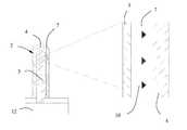
- FIG. 1is a schematic cross sectional view of an optoelectronic semiconductor device comprising quantum dots according to the invention
- FIG. 2schematically illustrates quantum dots arranged on the circumferential surface of the nanowire core
- FIG. 3schematically illustrates quantum dots embedded in an intermediate shell layer according to the invention
- FIG. 4is a cross sectional view of a portion of a nanowire comprising multiple concentric layers of quantum dots
- FIG. 5is a schematic cross sectional view of a portion of a nanowire comprising quantum dots embedded in the nanowire core.
- FIGS. 6 a - bschematically illustrates embodiments of the present invention comprising quantum dots adapted to absorb and reemit light produced in an active region.
- Nanowiresare usually interpreted as nanostructures that are of nanometer dimension in its diameter. As the term nanowire implies, it is the lateral size that is on the nanoscale whereas the longitudinal size is unconstrained. Such nanostructures are commonly also referred to as nanowhiskers, one-dimensional nanoelements, nanorods, etc. Although these terms imply an elongated shape the nanowires may be pyramidal or stub-like and since nanowires may have various cross-sectional shapes the diameter is in this application intended to refer to the effective diameter. Generally, nanowires are considered to have at least two dimensions each of which are not greater than 300 nm, but nanowires can have a diameter or width of up to about 1 ⁇ m.
- the one dimensional nature of the nanowiresprovides unique physical, optical and electronic properties. These properties can for example be used to form devices utilizing quantum mechanical effects or to form heterostructures of compositionally different materials that usually cannot be combined due to large lattice mismatch.
- One exampleis integration of semiconductor materials with reduced lattice-matching constraints, which for example allow the growth of III-V semiconductor nanowires on Si substrates.
- nanowiresprovide surfaces with low defect densities as templates for further epitaxial growth, which is a requirement for making quantum dots of homogeneous size and uniform distribution.
- an optoelectronic semiconductor devicecomprises at least one semiconductor nanowire 2 , which comprises at least a nanowire core 3 and at least a shell layer 4 arranged around at least a portion of the nanowire core 3 .
- the nanowire 2protrudes from a substrate 12 .
- the nanowire core 3 and the shell layer 4forms a pn or pin junction that in operation provides an active region 7 , i.e. the active region at least partly forms a depletion region between p and n regions of the pn or pin junction, for carrier generation or carrier recombination.
- Quantum dots 10are arranged at least in a region of the nanowire corresponding to the active region 7 in order to act as carrier recombination centres or carrier recombination centres.
- quantum dots 10By using the nanowire core 3 as template for further formation of the quantum dots 10 and the shell layer 4 , quantum dots 10 of homogeneous size and uniform distribution can be obtained.
- the optoelectronic semiconductor devicecan be used for light generation or light absorption.
- the optoelectronic semiconductor deviceis a light emitting diode, wherein the quantum dots 10 in the active region 7 in operation act as carrier recombination centres.
- the optoelectronic semiconductor deviceis a photoelectric device, such as a photo diode, a photo detector or a solar cell, wherein the quantum dots 10 in the active region 7 in operation act as carrier generation centres.
- the optoelectronic semiconductor deviceis described mostly in terms of an LED device.
- One embodiment of the present inventionis a nanostructured LED device comprising a nanowire 2 protruding from a substrate 12 .
- the nanowire 2comprises a shell layer 4 arranged around a nanowire core 3 forming a radial pn-junction contributing to the formation of an active region 7 at the interface between the shell layer 4 and the nanowire core 3 to produce light.
- the nanowire 2is made of nitride based III-V semiconductor materials, however the nanowire can also be made of non-nitride materials.
- the active region 7comprises quantum dots 10 adapted to act as recombination centres.
- the quantum dotsare uniformly distributed and having homogenous size.
- the nanowire core 3is an n-doped nitride based III-V semiconductor and the shell layer 4 is a p-doped nitride based III-V semiconductor.
- FIG. 2schematically illustrates one embodiment of a nanostructured LED device comprising a nanowire 2 of a III-N semiconductor material protruding from a semiconductor substrate 12 .
- the nanowire 2comprises a nanowire core 3 enclosed in a shell layer 4 forming a pn-junction that in operation provides an active region 7 to produce light.
- Quantum dots 10are in epitaxial connection to the circumferential surface of the nanowire core 3 and embedded in the shell layer 4 .
- the nanowire designis hereby adapted to make the quantum dots 10 function as recombination centres in the active region 7 . Thereby the wavelength of the generated light is essentially controlled by the size and spatial distribution of the quantum dots 10 .
- the quantum dots 10are of homogenous size and uniformly distributed to give a pre-determined wavelength of the produced light, which is to be emitted from the nanostructured LED device.
- the circumferential surfacemay comprise facets and/or edges which are suitable for quantum dot growth.
- FIG. 3illustrates another embodiment of a nanostructured LED device comprising a nanowire 2 having a nanowire core 3 and a shell layer 4 .
- Quantum dots 10are embedded in an intermediate shell layer 5 which is enclosed between the nanowire core 3 and the shell layer 4 .
- the active region 7(only shown in the enlarged view) is adapted to extend over the quantum dots 10 .
- the nanostructured LED devicemay comprise an n-GaN nanowire core 3 , an intermediate shell layer 5 of In x Ga 1-x N comprising embedded InGaN SK dots and a shell layer 4 of p-GaN.
- the SK dotsare uniformly distributed and of homogenous size, or have a pre-determined size distribution to provide light emission within a certain wavelength interval or at certain pre-determined wavelengths.
- nanowiresprovide surfaces with low defect densities, in principle defect-free surfaces, which can function as templates for further epitaxial growth. Accordingly the spatial distribution and size of the quantum dots 10 of the present invention is preferably uniform over a circumferential surface of the nanowire 2 . This is achieved by providing equal growth conditions over the whole surface. However, the growth conditions may be altered to accomplish any other pre-determined distribution along and around the nanowire 2 .
- the circumferential surfacemay comprises both facets and planar sub-surfaces and edges that are defined by the crystal structure of the nanowire material. The quantum dots can be grown selectively on these facets or edges.
- the quantum dots 10have a radial distribution.
- the quantum dots 10are arranged in a plurality of concentric layers, e.g. within an intermediate shell layer 5 , around the nanowire core 3 .
- Such concentric layerscan be accomplished by an alternating growth process: providing a first circumferential surface for quantum dot growth; growing quantum dots on the first circumferential surface; growing a first semiconductor layer enclosing the quantum dots 10 , the first semiconductor layer providing a second circumferential surface for quantum dot growth; growing quantum dots on the second circumferential surface; growing a second semiconductor layer enclosing the quantum dots 10 ; and growing a shell layer 4 to enclose the second semiconductor layer.
- the first and second semiconductor layersmake up the intermediate shell layer 5 and obviously the number of semiconductor layers, i.e. the number of concentric layer of quantum dots 10 , is not limited to two layers.
- the alternating growth processcan be iterated to obtain a pre-determined number of concentric layers, e.g.
- the active region of the LED devicemay extend over all quantum dot containing concentric layers or one or more concentric layers may each from an active region.
- a LED devicecomprising concentric layers comprising quantum dots that each emits light at different wavelength, i.e. different colours, can be provided.
- the nanostructured LED devicecomprises a nanowire core 3 enclosed by a shell layer 4 forming a pn-junction adapted to form an active region 7 to generate light.
- a plurality of concentric layers of quantum dots 10are embedded in the shell layer 4 adjacent to the nanowire core 3 in order to be comprised in the active region 7 when the LED is activated.
- FIG. 5schematically illustrates one embodiment of a nanostructured LED device in accordance with the present invention comprising a nanowire core 3 enclosed by a shell layer 4 forming a pn-junction adapted to form an active region 7 to generate light.
- Quantum dots 10are embedded in the nanowire core 3 adjacent to the shell layer 4 in order to be comprised in the active region 7 when the LED is activated.
- one embodiment of the present inventioncomprises a first concentric layer of quantum dots 10 grown on the circumferential surface of a nanowire core 3 and embedded in an intermediate shell layer 5 .
- a second concentric layer of quantum dots 10is grown on the circumferential surface of the intermediate shell layer 5 and embedded in a shell layer 4 .
- the size of the quantum dots 10 of a nanostructured LED device of the present inventioncan be altered from one concentric layer of quantum dots to another. This can for example be used to obtain light emission at a plurality of well defined wavelengths, e.g. RGB for white light output, or within a certain wavelength interval. In addition the size of the quantum dots 10 of different concentric layers can be different e.g. to adjust the wavelength of the emitted light of the nanostructured LED.
- the nanostructured LED devicecomprises a nanowire 2 protruding from a substrate 12 .
- a shell layer 4is arranged around a nanowire core 3 forming a radial pn-junction that can contribute to the formation of an active region 7 at the interface between the shell layer 4 and the nanowire core 3 in order to produce light.
- the active region 7comprises one or more concentric layer of quantum dots 10 adapted to act as carrier recombination centres or carrier generation centres and one or more concentric layer forming a quantum well.
- the concentric layers of quantum dots and the concentric layers forming quantum wellsare interchangeably stacked onto each other.
- Such an configuration of the active region 7may provide efficient light generation in certain wavelength regions such as a for the generation of blue light.
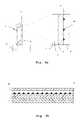
- a nanostructured LED devicetypically comprises an array of nanowires 2 protruding from a substrate to provide a useful light emission from the device.
- the substratemay comprise a buffer layer adjacent to the nanowires.
- the buffer layermay for example serve as a template for nanowire growth and can also be used to electrically connect the nanowire to a contact.
- Threading dislocationsmay occur in the nanowires 2 of the nanostructured LED device of the present invention, however the threading dislocation density is preferably less than 3 per nanowire 2 or preferably less than 5% of the nanowires 2 in a population on a substrate 12 comprises a threading dislocation.
- GaN bulk layers grown from substrates of e.g. Al 2 O 3 , Si or SiCgenerally show very high defect levels with threading dislocation densities of 10 7 -10 11 cm ⁇ 2 .
- the nitride based III-V semiconductor nanostructures according to the present inventioncan be considered to be fundamentally better templates/substrates for continued crystal growth than common bulk nitride based substrates.
- III-N nanowiresas templates for SK-dot growth a major cause for variation of local growth conditions due to defects and surface roughness distribution can be eliminated. This enables improved dot homogeneity concerning size, strain and compositional distribution and further also giving the possibility to better alter dot size by variation of growth conditions while retaining homogeneous dots.
- an optoelectronic semiconductor devicecomprises a nanowire 2 having a nanowire core 3 made of GaN and a shell layer 4 made of AlGaN.
- Quantum dots 10 made of GaNare embedded in the shell layer adjacent to the nanowire core 3 .
- SK dots incorporating Alare of interest for UV (ultra violet) applications above the fundamental bandgap of GaN (3.3 eV), but can also be used in higher bandgap applications.
- UV-lightultraviolet
- a nanostructured LED devicecomprising In x Ga 1-x N quantum dots 10 that provides light emission in the infra-red to green wavelength region with improved emission.
- one such nanostructured LED devicecomprises a nanowire core made of GaN and InGaN dots embedded in GaN.
- a nanostructured LED device of the present inventionpreferably comprises nitride based III-V semiconductors comprising any or a combination of Ga, In, Al or B. More preferably the nanowire core 2 , the quantum dots 10 , the shell layer 4 and the intermediate shell layer 5 is preferably comprising any, or a combination of, AlInGaN, AlGaN, InGaN, InN, AlN or GaN.
- the nanostructured LED devicecomprises a n-AlGaN nanowire core 3 enclosed in an intermediate shell layer 5 of AlGaN comprising embedded GaN SK dots 10 and a shell layer 4 of AlGaN.
- This embodimentis suitable for making LEDs emitting UV to blue light.
- the nanostructured LED devicecomprises an n-GaN nanowire core 3 enclosed in an intermediate shell layer 5 of In x Ga 1-x N comprising embedded In y Ga 1-y N SK dots 10 and a shell layer 4 of p-GaN.
- a dielectric layerfor example made of silicon nitride, can be used as a growth mask.
- a LED deviceis made using materials from the GaN system and is adapted to emit blue light from an active region 7 .
- the active region 7may be without quantum dots.
- the LED device according to this embodimentfurther comprises an absorption layer 14 that comprises SK dots 10 , preferably homogenously distributed and of uniform size.
- the SK dotsare adapted to absorb and reemit light in colours defined by the quantum well energies of the quantum dots. In prior art phosphors are used to accomplish this absorption.
- the absorption layer 14can be provided in nanowire based LEDs according to the present invention or LEDs fabricated using planar technology, as illustrated in FIGS. 6 a and 6 b , respectively.
- a plurality of absorption layers 14 of quantum dots 10may be arranged in connection to the active region 7 .
- the dot-containing absorption layer 14should have a lower bandgap than the exciting light and to increase absorption-efficiency it may be advantageous to place it between a reflector and the active region 7 of the LED so that light passes through it twice.
- an optoelectronic semiconductor deviceis a laser diode, wherein a narrow wavelength peak is desired.
- the nanowire technologymakes it possible to provide uniformly sized and distributed quantum dots with controlled composition and strain. Thereby the emitted light can be tailored to be within a narrow wavelength interval and at different wavelengths, with a high efficiency, than is possible with conventional technology.
- Optoelectronic semiconductor devices comprising quantum dots according to the present inventionmay comprise non nitride semiconductor materials comprising any, or a combination of, III-V, IV or II-VI semiconductor materials.
- a compound consisting of an element A and an element Bis commonly denoted AB, which should be interpreted as A x B 1-x .
Landscapes
- Chemical & Material Sciences (AREA)
- Engineering & Computer Science (AREA)
- Nanotechnology (AREA)
- Physics & Mathematics (AREA)
- Life Sciences & Earth Sciences (AREA)
- Biophysics (AREA)
- Optics & Photonics (AREA)
- Crystallography & Structural Chemistry (AREA)
- Led Device Packages (AREA)
- Led Devices (AREA)
Abstract
Description
Claims (20)
Applications Claiming Priority (4)
| Application Number | Priority Date | Filing Date | Title |
|---|---|---|---|
| SE0801649-5 | 2008-07-09 | ||
| SE0801649ASE533090C2 (en) | 2008-07-09 | 2008-07-09 | Nanostructured LED |
| SE0801649 | 2008-07-09 | ||
| PCT/SE2009/050858WO2010005381A1 (en) | 2008-07-09 | 2009-07-02 | Optoelectronic semiconductor device |
Related Parent Applications (1)
| Application Number | Title | Priority Date | Filing Date |
|---|---|---|---|
| PCT/SE2009/050858ContinuationWO2010005381A1 (en) | 2008-07-09 | 2009-07-02 | Optoelectronic semiconductor device |
Publications (2)
| Publication Number | Publication Date |
|---|---|
| US20100006817A1 US20100006817A1 (en) | 2010-01-14 |
| US8138493B2true US8138493B2 (en) | 2012-03-20 |
Family
ID=41504312
Family Applications (1)
| Application Number | Title | Priority Date | Filing Date |
|---|---|---|---|
| US12/499,491Expired - Fee RelatedUS8138493B2 (en) | 2008-07-09 | 2009-07-08 | Optoelectronic semiconductor device |
Country Status (1)
| Country | Link |
|---|---|
| US (1) | US8138493B2 (en) |
Cited By (9)
| Publication number | Priority date | Publication date | Assignee | Title |
|---|---|---|---|---|
| US8551834B2 (en) | 2006-09-18 | 2013-10-08 | Qunano Ab | Method of producing precision vertical and horizontal layers in a vertical semiconductor structure |
| WO2015095049A1 (en) | 2013-12-17 | 2015-06-25 | Glo Ab | Iii-nitride nanowire led with strain modified surface active region and method of making thereof |
| US9099573B2 (en) | 2013-10-31 | 2015-08-04 | Samsung Electronics Co., Ltd. | Nano-structure semiconductor light emitting device |
| WO2016025325A1 (en) | 2014-08-12 | 2016-02-18 | Glo Ab | Iii-nitride nanowire led with strain modified surface active region and method of making thereof |
| US20160056331A1 (en)* | 2014-08-25 | 2016-02-25 | Jung Sub Kim | Nanostructure semiconductor light emitting device |
| US9362448B2 (en) | 2014-09-05 | 2016-06-07 | Samsung Electronics Co., Ltd. | Nanostructure semiconductor light emitting device |
| US9673236B2 (en) | 2014-04-29 | 2017-06-06 | Samsung Electronics Co., Ltd. | Pixel array of an image sensor and image sensor |
| US10615299B2 (en) | 2014-09-30 | 2020-04-07 | Commissariat à l'énergie atomique et aux énergies alternatives | Optoelectronic device with three-dimensional semiconductor elements |
| US11610934B2 (en) | 2016-12-19 | 2023-03-21 | Samsung Display Co., Ltd. | Light emitting device and manufacturing method of the light emitting device |
Families Citing this family (42)
| Publication number | Priority date | Publication date | Assignee | Title |
|---|---|---|---|---|
| WO2008079078A1 (en)* | 2006-12-22 | 2008-07-03 | Qunano Ab | Elevated led and method of producing such |
| US8274039B2 (en) | 2008-11-13 | 2012-09-25 | Zena Technologies, Inc. | Vertical waveguides with various functionality on integrated circuits |
| US9000353B2 (en) | 2010-06-22 | 2015-04-07 | President And Fellows Of Harvard College | Light absorption and filtering properties of vertically oriented semiconductor nano wires |
| US8384007B2 (en)* | 2009-10-07 | 2013-02-26 | Zena Technologies, Inc. | Nano wire based passive pixel image sensor |
| US8269985B2 (en) | 2009-05-26 | 2012-09-18 | Zena Technologies, Inc. | Determination of optimal diameters for nanowires |
| US8546742B2 (en) | 2009-06-04 | 2013-10-01 | Zena Technologies, Inc. | Array of nanowires in a single cavity with anti-reflective coating on substrate |
| US8507840B2 (en) | 2010-12-21 | 2013-08-13 | Zena Technologies, Inc. | Vertically structured passive pixel arrays and methods for fabricating the same |
| US9082673B2 (en) | 2009-10-05 | 2015-07-14 | Zena Technologies, Inc. | Passivated upstanding nanostructures and methods of making the same |
| US8229255B2 (en) | 2008-09-04 | 2012-07-24 | Zena Technologies, Inc. | Optical waveguides in image sensors |
| US8735797B2 (en) | 2009-12-08 | 2014-05-27 | Zena Technologies, Inc. | Nanowire photo-detector grown on a back-side illuminated image sensor |
| US9299866B2 (en) | 2010-12-30 | 2016-03-29 | Zena Technologies, Inc. | Nanowire array based solar energy harvesting device |
| US9478685B2 (en) | 2014-06-23 | 2016-10-25 | Zena Technologies, Inc. | Vertical pillar structured infrared detector and fabrication method for the same |
| US8748799B2 (en) | 2010-12-14 | 2014-06-10 | Zena Technologies, Inc. | Full color single pixel including doublet or quadruplet si nanowires for image sensors |
| US8890271B2 (en) | 2010-06-30 | 2014-11-18 | Zena Technologies, Inc. | Silicon nitride light pipes for image sensors |
| US9406709B2 (en) | 2010-06-22 | 2016-08-02 | President And Fellows Of Harvard College | Methods for fabricating and using nanowires |
| US8866065B2 (en) | 2010-12-13 | 2014-10-21 | Zena Technologies, Inc. | Nanowire arrays comprising fluorescent nanowires |
| US8889455B2 (en) | 2009-12-08 | 2014-11-18 | Zena Technologies, Inc. | Manufacturing nanowire photo-detector grown on a back-side illuminated image sensor |
| US8791470B2 (en) | 2009-10-05 | 2014-07-29 | Zena Technologies, Inc. | Nano structured LEDs |
| US8835831B2 (en) | 2010-06-22 | 2014-09-16 | Zena Technologies, Inc. | Polarized light detecting device and fabrication methods of the same |
| US8299472B2 (en) | 2009-12-08 | 2012-10-30 | Young-June Yu | Active pixel sensor with nanowire structured photodetectors |
| US9515218B2 (en) | 2008-09-04 | 2016-12-06 | Zena Technologies, Inc. | Vertical pillar structured photovoltaic devices with mirrors and optical claddings |
| US8519379B2 (en) | 2009-12-08 | 2013-08-27 | Zena Technologies, Inc. | Nanowire structured photodiode with a surrounding epitaxially grown P or N layer |
| US9343490B2 (en) | 2013-08-09 | 2016-05-17 | Zena Technologies, Inc. | Nanowire structured color filter arrays and fabrication method of the same |
| US9005548B2 (en)* | 2009-02-25 | 2015-04-14 | California Institute Of Technology | Methods for fabricating high aspect ratio probes and deforming high aspect ratio nanopillars and micropillars |
| EP2502264A4 (en) | 2009-11-19 | 2015-09-16 | California Inst Of Techn | METHODS OF MANUFACTURING SELF-ALIGNMENT DEVICES ON SEMICONDUCTORS |
| US9018684B2 (en) | 2009-11-23 | 2015-04-28 | California Institute Of Technology | Chemical sensing and/or measuring devices and methods |
| US9112085B2 (en)* | 2009-11-30 | 2015-08-18 | The Royal Institution For The Advancement Of Learning/Mcgill University | High efficiency broadband semiconductor nanowire devices |
| CA2802539A1 (en)* | 2010-06-18 | 2011-12-22 | Glo Ab | Nanowire led structure and method for manufacturing the same |
| WO2012035243A1 (en) | 2010-09-14 | 2012-03-22 | Commissariat A L'energie Atomique Et Aux Energies Alternatives | Nanowire-based optoelectronic device for light emission |
| FR2964796B1 (en)* | 2010-09-14 | 2014-03-21 | Commissariat Energie Atomique | AN OPTOELECTRONIC DEVICE BASED ON NANOWLAS FOR LIGHT EMISSION |
| US8484756B2 (en)* | 2011-01-19 | 2013-07-09 | The United States of America, as represented by the Secretary of Commerce, The National Institute of Standards and Technology | Tip-mounted nanowire light source instrumentation |
| US8148252B1 (en)* | 2011-03-02 | 2012-04-03 | S.O.I. Tec Silicon On Insulator Technologies | Methods of forming III/V semiconductor materials, and semiconductor structures formed using such methods |
| KR101967836B1 (en) | 2012-12-14 | 2019-04-10 | 삼성전자주식회사 | 3-Dimesional Light Emitting device and fabrication thereof |
| FR3000612B1 (en)* | 2012-12-28 | 2016-05-06 | Commissariat Energie Atomique | OPTOELECTRONIC MICROFILL OR NANOWIL DEVICE |
| US20140264261A1 (en)* | 2013-03-14 | 2014-09-18 | Michael A. Mastro | Light emitting device on metal foam substrate |
| WO2014143991A1 (en)* | 2013-03-15 | 2014-09-18 | Glo Ab | Nanowire led structure with decreased leakage and method of making same |
| US9196787B2 (en) | 2013-06-07 | 2015-11-24 | Glo Ab | Nanowire LED structure with decreased leakage and method of making same |
| WO2015115446A1 (en)* | 2014-01-28 | 2015-08-06 | 住友化学株式会社 | Method for controlling harmful organisms |
| EP2947045B1 (en)* | 2014-05-19 | 2019-08-28 | IMEC vzw | Low defect-density vertical nanowire semiconductor structures and method for making such structures |
| US10483319B2 (en) | 2014-08-08 | 2019-11-19 | Glo Ab | Pixilated display device based upon nanowire LEDs and method for making the same |
| US9620559B2 (en) | 2014-09-26 | 2017-04-11 | Glo Ab | Monolithic image chip for near-to-eye display |
| US10790400B2 (en)* | 2015-09-08 | 2020-09-29 | Addventure Support Enterprises, Inc. | Solar cells that include quantum dots |
Citations (4)
| Publication number | Priority date | Publication date | Assignee | Title |
|---|---|---|---|---|
| US20060021647A1 (en)* | 2004-07-28 | 2006-02-02 | Gui John Y | Molecular photovoltaics, method of manufacture and articles derived therefrom |
| US20080036038A1 (en)* | 2006-03-10 | 2008-02-14 | Hersee Stephen D | PULSED GROWTH OF CATALYST-FREE GROWITH OF GaN NANOWIRES AND APPLICATION IN GROUP III NITRIDE SEMICONDUCTOR BULK MATERIAL |
| US7335908B2 (en) | 2002-07-08 | 2008-02-26 | Qunano Ab | Nanostructures and methods for manufacturing the same |
| US20100019252A1 (en) | 2008-07-24 | 2010-01-28 | Alexandre Bratkovski | Nanowire-Based Light-Emitting Diodes and Light-Detection Devices With Nanocrystalline Outer Surface |
- 2009
- 2009-07-08USUS12/499,491patent/US8138493B2/ennot_activeExpired - Fee Related
Patent Citations (4)
| Publication number | Priority date | Publication date | Assignee | Title |
|---|---|---|---|---|
| US7335908B2 (en) | 2002-07-08 | 2008-02-26 | Qunano Ab | Nanostructures and methods for manufacturing the same |
| US20060021647A1 (en)* | 2004-07-28 | 2006-02-02 | Gui John Y | Molecular photovoltaics, method of manufacture and articles derived therefrom |
| US20080036038A1 (en)* | 2006-03-10 | 2008-02-14 | Hersee Stephen D | PULSED GROWTH OF CATALYST-FREE GROWITH OF GaN NANOWIRES AND APPLICATION IN GROUP III NITRIDE SEMICONDUCTOR BULK MATERIAL |
| US20100019252A1 (en) | 2008-07-24 | 2010-01-28 | Alexandre Bratkovski | Nanowire-Based Light-Emitting Diodes and Light-Detection Devices With Nanocrystalline Outer Surface |
Cited By (18)
| Publication number | Priority date | Publication date | Assignee | Title |
|---|---|---|---|---|
| US8551834B2 (en) | 2006-09-18 | 2013-10-08 | Qunano Ab | Method of producing precision vertical and horizontal layers in a vertical semiconductor structure |
| US9087896B2 (en) | 2006-09-18 | 2015-07-21 | Qunano Ab | Method of producing precision vertical and horizontal layers in a vertical semiconductor structure |
| US9257605B2 (en) | 2013-10-31 | 2016-02-09 | Samsung Electronics Co., Ltd. | Nano-structure semiconductor light emitting device |
| US9099573B2 (en) | 2013-10-31 | 2015-08-04 | Samsung Electronics Co., Ltd. | Nano-structure semiconductor light emitting device |
| US9761757B2 (en) | 2013-12-17 | 2017-09-12 | Glo Ab | III-nitride nanowire LED with strain modified surface active region and method of making thereof |
| US10026866B2 (en) | 2013-12-17 | 2018-07-17 | Glo Ab | III-nitride nanowire LED with strain modified surface active region and method of making thereof |
| US9281442B2 (en) | 2013-12-17 | 2016-03-08 | Glo Ab | III-nitride nanowire LED with strain modified surface active region and method of making thereof |
| WO2015095049A1 (en) | 2013-12-17 | 2015-06-25 | Glo Ab | Iii-nitride nanowire led with strain modified surface active region and method of making thereof |
| US9673236B2 (en) | 2014-04-29 | 2017-06-06 | Samsung Electronics Co., Ltd. | Pixel array of an image sensor and image sensor |
| WO2016025325A1 (en) | 2014-08-12 | 2016-02-18 | Glo Ab | Iii-nitride nanowire led with strain modified surface active region and method of making thereof |
| US9882086B2 (en) | 2014-08-12 | 2018-01-30 | Glo Ab | III-nitride nanowire LED with strain modified surface active region and method of making thereof |
| US9748438B2 (en) | 2014-08-25 | 2017-08-29 | Samsung Electronics Co., Ltd. | Nanostructure semiconductor light emitting device |
| US9406839B2 (en)* | 2014-08-25 | 2016-08-02 | Samsung Electronics Co., Ltd. | Nanostructure semiconductor light emitting device |
| US20160056331A1 (en)* | 2014-08-25 | 2016-02-25 | Jung Sub Kim | Nanostructure semiconductor light emitting device |
| US9362448B2 (en) | 2014-09-05 | 2016-06-07 | Samsung Electronics Co., Ltd. | Nanostructure semiconductor light emitting device |
| US10615299B2 (en) | 2014-09-30 | 2020-04-07 | Commissariat à l'énergie atomique et aux énergies alternatives | Optoelectronic device with three-dimensional semiconductor elements |
| US11610934B2 (en) | 2016-12-19 | 2023-03-21 | Samsung Display Co., Ltd. | Light emitting device and manufacturing method of the light emitting device |
| US12283604B2 (en) | 2016-12-19 | 2025-04-22 | Samsung Display Co., Ltd. | Light emitting device and manufacturing method of the light emitting device |
Also Published As
| Publication number | Publication date |
|---|---|
| US20100006817A1 (en) | 2010-01-14 |
Similar Documents
| Publication | Publication Date | Title |
|---|---|---|
| US8138493B2 (en) | Optoelectronic semiconductor device | |
| EP2297785B1 (en) | Optoelectronic semiconductor device | |
| US10026866B2 (en) | III-nitride nanowire LED with strain modified surface active region and method of making thereof | |
| JP4786691B2 (en) | Semiconductor device and manufacturing method thereof | |
| CN107251239B (en) | III valence nitride nanowires and its manufacturing method with strain modified surface active region | |
| CN110678990B (en) | Nano-structure | |
| US20090159869A1 (en) | Solid State Light Emitting Device | |
| US20220352398A1 (en) | Composition of matter | |
| KR100495824B1 (en) | Semiconductor LED device | |
| WO2024042221A1 (en) | Nanostructure/microstructure device | |
| Nasir et al. | Recent Advancement on Crystalline quality, IQE, and EQE of III-nitride-based deep-ultraviolet light-emitting diodes: Comprehensive Review | |
| Samuelson | Nanowire LEDs and Solar Cells | |
| Samuelson | Nanowire-based LEDs and photovoltaics | |
| KR20230162568A (en) | Ultraviolet light emitting device and method for manufacturing the same | |
| Su et al. | Optical characterization of InGaN/GaN multiple quantum well structures grown by metalorganic chemical vapor deposition |
Legal Events
| Date | Code | Title | Description |
|---|---|---|---|
| AS | Assignment | Owner name:QUNANO AB, SWEDEN Free format text:ASSIGNMENT OF ASSIGNORS INTEREST;ASSIGNORS:OHLSSON, JONAS;SAMUELSON, LARS;REEL/FRAME:023269/0743;SIGNING DATES FROM 20090703 TO 20090720 Owner name:QUNANO AB, SWEDEN Free format text:ASSIGNMENT OF ASSIGNORS INTEREST;ASSIGNORS:OHLSSON, JONAS;SAMUELSON, LARS;SIGNING DATES FROM 20090703 TO 20090720;REEL/FRAME:023269/0743 | |
| ZAAA | Notice of allowance and fees due | Free format text:ORIGINAL CODE: NOA | |
| ZAAB | Notice of allowance mailed | Free format text:ORIGINAL CODE: MN/=. | |
| STCF | Information on status: patent grant | Free format text:PATENTED CASE | |
| FPAY | Fee payment | Year of fee payment:4 | |
| AS | Assignment | Owner name:HERCULES CAPITAL, INC., AS ADMINISTRATIVE AGENT, M Free format text:ASSIGNMENT OF IP SECURITY AGREEMENT;ASSIGNOR:GLO AB;REEL/FRAME:049042/0527 Effective date:20180108 Owner name:HERCULES CAPITAL, INC., AS ADMINISTRATIVE AGENT, MASSACHUSETTS Free format text:ASSIGNMENT OF IP SECURITY AGREEMENT;ASSIGNOR:GLO AB;REEL/FRAME:049042/0527 Effective date:20180108 | |
| FEPP | Fee payment procedure | Free format text:MAINTENANCE FEE REMINDER MAILED (ORIGINAL EVENT CODE: REM.); ENTITY STATUS OF PATENT OWNER: SMALL ENTITY | |
| FEPP | Fee payment procedure | Free format text:7.5 YR SURCHARGE - LATE PMT W/IN 6 MO, SMALL ENTITY (ORIGINAL EVENT CODE: M2555); ENTITY STATUS OF PATENT OWNER: SMALL ENTITY | |
| MAFP | Maintenance fee payment | Free format text:PAYMENT OF MAINTENANCE FEE, 8TH YR, SMALL ENTITY (ORIGINAL EVENT CODE: M2552); ENTITY STATUS OF PATENT OWNER: SMALL ENTITY Year of fee payment:8 | |
| FEPP | Fee payment procedure | Free format text:MAINTENANCE FEE REMINDER MAILED (ORIGINAL EVENT CODE: REM.); ENTITY STATUS OF PATENT OWNER: SMALL ENTITY | |
| LAPS | Lapse for failure to pay maintenance fees | Free format text:PATENT EXPIRED FOR FAILURE TO PAY MAINTENANCE FEES (ORIGINAL EVENT CODE: EXP.); ENTITY STATUS OF PATENT OWNER: SMALL ENTITY | |
| STCH | Information on status: patent discontinuation | Free format text:PATENT EXPIRED DUE TO NONPAYMENT OF MAINTENANCE FEES UNDER 37 CFR 1.362 | |
| FP | Lapsed due to failure to pay maintenance fee | Effective date:20240320 |