US8138037B2 - Method and structure for gate height scaling with high-k/metal gate technology - Google Patents
Method and structure for gate height scaling with high-k/metal gate technologyDownload PDFInfo
- Publication number
- US8138037B2 US8138037B2US12/715,781US71578110AUS8138037B2US 8138037 B2US8138037 B2US 8138037B2US 71578110 AUS71578110 AUS 71578110AUS 8138037 B2US8138037 B2US 8138037B2
- Authority
- US
- United States
- Prior art keywords
- gate
- layer
- forming
- polysilicon
- dummy gate
- Prior art date
- Legal status (The legal status is an assumption and is not a legal conclusion. Google has not performed a legal analysis and makes no representation as to the accuracy of the status listed.)
- Expired - Fee Related, expires
Links
- 238000000034methodMethods0.000titleclaimsabstractdescription57
- 229910052751metalInorganic materials0.000titleclaimsabstractdescription53
- 239000002184metalSubstances0.000titleclaimsabstractdescription53
- 238000005516engineering processMethods0.000titledescription3
- 229910021420polycrystalline siliconInorganic materials0.000claimsabstractdescription74
- 229920005591polysiliconPolymers0.000claimsabstractdescription74
- XUIMIQQOPSSXEZ-UHFFFAOYSA-NSiliconChemical compound[Si]XUIMIQQOPSSXEZ-UHFFFAOYSA-N0.000claimsdescription26
- 230000004888barrier functionEffects0.000claimsdescription26
- 229910052710siliconInorganic materials0.000claimsdescription26
- 239000010703siliconSubstances0.000claimsdescription26
- 229910021332silicideInorganic materials0.000claimsdescription21
- FVBUAEGBCNSCDD-UHFFFAOYSA-Nsilicide(4-)Chemical compound[Si-4]FVBUAEGBCNSCDD-UHFFFAOYSA-N0.000claimsdescription19
- 239000000758substrateSubstances0.000claimsdescription18
- 239000004065semiconductorSubstances0.000claimsdescription15
- 238000002955isolationMethods0.000claimsdescription7
- 230000000873masking effectEffects0.000claimsdescription6
- 238000000059patterningMethods0.000claimsdescription5
- 238000013461designMethods0.000description56
- 230000008569processEffects0.000description21
- 238000012938design processMethods0.000description14
- 238000004519manufacturing processMethods0.000description14
- 239000000463materialSubstances0.000description12
- 238000005229chemical vapour depositionMethods0.000description11
- 238000012545processingMethods0.000description10
- 238000004088simulationMethods0.000description8
- 238000012360testing methodMethods0.000description8
- 229920002120photoresistant polymerPolymers0.000description7
- VYPSYNLAJGMNEJ-UHFFFAOYSA-NSilicium dioxideChemical compoundO=[Si]=OVYPSYNLAJGMNEJ-UHFFFAOYSA-N0.000description6
- 238000000151depositionMethods0.000description6
- 125000006850spacer groupChemical group0.000description6
- 238000000623plasma-assisted chemical vapour depositionMethods0.000description5
- KRHYYFGTRYWZRS-UHFFFAOYSA-NFluoraneChemical compoundFKRHYYFGTRYWZRS-UHFFFAOYSA-N0.000description4
- PXHVJJICTQNCMI-UHFFFAOYSA-NNickelChemical compound[Ni]PXHVJJICTQNCMI-UHFFFAOYSA-N0.000description4
- 238000003860storageMethods0.000description4
- 229910000577Silicon-germaniumInorganic materials0.000description3
- 230000005540biological transmissionEffects0.000description3
- 230000008021depositionEffects0.000description3
- 230000006870functionEffects0.000description3
- 238000012986modificationMethods0.000description3
- 230000004048modificationEffects0.000description3
- 239000000377silicon dioxideSubstances0.000description3
- VHUUQVKOLVNVRT-UHFFFAOYSA-NAmmonium hydroxideChemical compound[NH4+].[OH-]VHUUQVKOLVNVRT-UHFFFAOYSA-N0.000description2
- BOTDANWDWHJENH-UHFFFAOYSA-NTetraethyl orthosilicateChemical compoundCCO[Si](OCC)(OCC)OCCBOTDANWDWHJENH-UHFFFAOYSA-N0.000description2
- 238000004458analytical methodMethods0.000description2
- 238000000137annealingMethods0.000description2
- 238000013459approachMethods0.000description2
- 239000005380borophosphosilicate glassSubstances0.000description2
- -1but not limited toSubstances0.000description2
- 239000007795chemical reaction productSubstances0.000description2
- 229910052681coesiteInorganic materials0.000description2
- 238000007796conventional methodMethods0.000description2
- 229910052906cristobaliteInorganic materials0.000description2
- 238000013500data storageMethods0.000description2
- 238000005137deposition processMethods0.000description2
- 238000010586diagramMethods0.000description2
- 230000009977dual effectEffects0.000description2
- 229910052735hafniumInorganic materials0.000description2
- VBJZVLUMGGDVMO-UHFFFAOYSA-Nhafnium atomChemical compound[Hf]VBJZVLUMGGDVMO-UHFFFAOYSA-N0.000description2
- 125000001475halogen functional groupChemical group0.000description2
- 239000007943implantSubstances0.000description2
- 239000012212insulatorSubstances0.000description2
- QPJSUIGXIBEQAC-UHFFFAOYSA-Nn-(2,4-dichloro-5-propan-2-yloxyphenyl)acetamideChemical compoundCC(C)OC1=CC(NC(C)=O)=C(Cl)C=C1ClQPJSUIGXIBEQAC-UHFFFAOYSA-N0.000description2
- 229910052759nickelInorganic materials0.000description2
- 229910021334nickel silicideInorganic materials0.000description2
- RUFLMLWJRZAWLJ-UHFFFAOYSA-Nnickel silicideChemical compound[Ni]=[Si]=[Ni]RUFLMLWJRZAWLJ-UHFFFAOYSA-N0.000description2
- 230000003647oxidationEffects0.000description2
- 238000007254oxidation reactionMethods0.000description2
- 238000005240physical vapour depositionMethods0.000description2
- 239000000047productSubstances0.000description2
- 229910052682stishoviteInorganic materials0.000description2
- 229910052905tridymiteInorganic materials0.000description2
- 238000012795verificationMethods0.000description2
- WKBOTKDWSSQWDR-UHFFFAOYSA-NBromine atomChemical compound[Br]WKBOTKDWSSQWDR-UHFFFAOYSA-N0.000description1
- ZAMOUSCENKQFHK-UHFFFAOYSA-NChlorine atomChemical compound[Cl]ZAMOUSCENKQFHK-UHFFFAOYSA-N0.000description1
- BPQQTUXANYXVAA-UHFFFAOYSA-NOrthosilicateChemical compound[O-][Si]([O-])([O-])[O-]BPQQTUXANYXVAA-UHFFFAOYSA-N0.000description1
- 229910003811SiGeCInorganic materials0.000description1
- RTAQQCXQSZGOHL-UHFFFAOYSA-NTitaniumChemical compound[Ti]RTAQQCXQSZGOHL-UHFFFAOYSA-N0.000description1
- NRTOMJZYCJJWKI-UHFFFAOYSA-NTitanium nitrideChemical compound[Ti]#NNRTOMJZYCJJWKI-UHFFFAOYSA-N0.000description1
- QCWXUUIWCKQGHC-UHFFFAOYSA-NZirconiumChemical compound[Zr]QCWXUUIWCKQGHC-UHFFFAOYSA-N0.000description1
- LEVVHYCKPQWKOP-UHFFFAOYSA-N[Si].[Ge]Chemical compound[Si].[Ge]LEVVHYCKPQWKOP-UHFFFAOYSA-N0.000description1
- 239000000908ammonium hydroxideSubstances0.000description1
- 230000008901benefitEffects0.000description1
- 230000015572biosynthetic processEffects0.000description1
- GDTBXPJZTBHREO-UHFFFAOYSA-NbromineSubstancesBrBrGDTBXPJZTBHREO-UHFFFAOYSA-N0.000description1
- 229910052794bromiumInorganic materials0.000description1
- 238000005266castingMethods0.000description1
- 239000000919ceramicSubstances0.000description1
- 238000012512characterization methodMethods0.000description1
- 229910052801chlorineInorganic materials0.000description1
- 239000000460chlorineSubstances0.000description1
- 239000010941cobaltSubstances0.000description1
- 229910017052cobaltInorganic materials0.000description1
- GUTLYIVDDKVIGB-UHFFFAOYSA-Ncobalt atomChemical compound[Co]GUTLYIVDDKVIGB-UHFFFAOYSA-N0.000description1
- 238000011960computer-aided designMethods0.000description1
- 239000004020conductorSubstances0.000description1
- 230000007812deficiencyEffects0.000description1
- 239000003989dielectric materialSubstances0.000description1
- 239000007772electrode materialSubstances0.000description1
- 238000005530etchingMethods0.000description1
- 229910000449hafnium oxideInorganic materials0.000description1
- WIHZLLGSGQNAGK-UHFFFAOYSA-Nhafnium(4+);oxygen(2-)Chemical compound[O-2].[O-2].[Hf+4]WIHZLLGSGQNAGK-UHFFFAOYSA-N0.000description1
- 230000010354integrationEffects0.000description1
- 239000013067intermediate productSubstances0.000description1
- 150000002500ionsChemical class0.000description1
- 238000012804iterative processMethods0.000description1
- 238000001459lithographyMethods0.000description1
- 230000007246mechanismEffects0.000description1
- 150000002739metalsChemical class0.000description1
- 229910003465moissaniteInorganic materials0.000description1
- 238000000465mouldingMethods0.000description1
- 230000006855networkingEffects0.000description1
- PEUPIGGLJVUNEU-UHFFFAOYSA-Nnickel siliconChemical compound[Si].[Ni]PEUPIGGLJVUNEU-UHFFFAOYSA-N0.000description1
- 230000003287optical effectEffects0.000description1
- 238000005457optimizationMethods0.000description1
- 230000003071parasitic effectEffects0.000description1
- 238000005498polishingMethods0.000description1
- 238000009877renderingMethods0.000description1
- 229910010271silicon carbideInorganic materials0.000description1
- 235000012239silicon dioxideNutrition0.000description1
- 238000004544sputter depositionMethods0.000description1
- 239000000126substanceSubstances0.000description1
- 230000002194synthesizing effectEffects0.000description1
- 229910052715tantalumInorganic materials0.000description1
- GUVRBAGPIYLISA-UHFFFAOYSA-Ntantalum atomChemical compound[Ta]GUVRBAGPIYLISA-UHFFFAOYSA-N0.000description1
- VSSLEOGOUUKTNN-UHFFFAOYSA-Ntantalum titaniumChemical compound[Ti].[Ta]VSSLEOGOUUKTNN-UHFFFAOYSA-N0.000description1
- 238000002076thermal analysis methodMethods0.000description1
- 239000010936titaniumSubstances0.000description1
- 229910052719titaniumInorganic materials0.000description1
- WFKWXMTUELFFGS-UHFFFAOYSA-NtungstenChemical compound[W]WFKWXMTUELFFGS-UHFFFAOYSA-N0.000description1
- 229910052721tungstenInorganic materials0.000description1
- 239000010937tungstenSubstances0.000description1
- 229910052726zirconiumInorganic materials0.000description1
Images


Classifications
- H—ELECTRICITY
- H10—SEMICONDUCTOR DEVICES; ELECTRIC SOLID-STATE DEVICES NOT OTHERWISE PROVIDED FOR
- H10D—INORGANIC ELECTRIC SEMICONDUCTOR DEVICES
- H10D64/00—Electrodes of devices having potential barriers
- H10D64/01—Manufacture or treatment
- H10D64/017—Manufacture or treatment using dummy gates in processes wherein at least parts of the final gates are self-aligned to the dummy gates, i.e. replacement gate processes
- H—ELECTRICITY
- H10—SEMICONDUCTOR DEVICES; ELECTRIC SOLID-STATE DEVICES NOT OTHERWISE PROVIDED FOR
- H10D—INORGANIC ELECTRIC SEMICONDUCTOR DEVICES
- H10D64/00—Electrodes of devices having potential barriers
- H10D64/60—Electrodes characterised by their materials
- H10D64/66—Electrodes having a conductor capacitively coupled to a semiconductor by an insulator, e.g. MIS electrodes
- H10D64/667—Electrodes having a conductor capacitively coupled to a semiconductor by an insulator, e.g. MIS electrodes the conductor comprising a layer of alloy material, compound material or organic material contacting the insulator, e.g. TiN workfunction layers
- H—ELECTRICITY
- H10—SEMICONDUCTOR DEVICES; ELECTRIC SOLID-STATE DEVICES NOT OTHERWISE PROVIDED FOR
- H10D—INORGANIC ELECTRIC SEMICONDUCTOR DEVICES
- H10D84/00—Integrated devices formed in or on semiconductor substrates that comprise only semiconducting layers, e.g. on Si wafers or on GaAs-on-Si wafers
- H10D84/01—Manufacture or treatment
- H10D84/0123—Integrating together multiple components covered by H10D12/00 or H10D30/00, e.g. integrating multiple IGBTs
- H10D84/0126—Integrating together multiple components covered by H10D12/00 or H10D30/00, e.g. integrating multiple IGBTs the components including insulated gates, e.g. IGFETs
- H10D84/0135—Manufacturing their gate conductors
- H—ELECTRICITY
- H10—SEMICONDUCTOR DEVICES; ELECTRIC SOLID-STATE DEVICES NOT OTHERWISE PROVIDED FOR
- H10D—INORGANIC ELECTRIC SEMICONDUCTOR DEVICES
- H10D84/00—Integrated devices formed in or on semiconductor substrates that comprise only semiconducting layers, e.g. on Si wafers or on GaAs-on-Si wafers
- H10D84/01—Manufacture or treatment
- H10D84/02—Manufacture or treatment characterised by using material-based technologies
- H10D84/03—Manufacture or treatment characterised by using material-based technologies using Group IV technology, e.g. silicon technology or silicon-carbide [SiC] technology
- H10D84/038—Manufacture or treatment characterised by using material-based technologies using Group IV technology, e.g. silicon technology or silicon-carbide [SiC] technology using silicon technology, e.g. SiGe
- H—ELECTRICITY
- H10—SEMICONDUCTOR DEVICES; ELECTRIC SOLID-STATE DEVICES NOT OTHERWISE PROVIDED FOR
- H10D—INORGANIC ELECTRIC SEMICONDUCTOR DEVICES
- H10D84/00—Integrated devices formed in or on semiconductor substrates that comprise only semiconducting layers, e.g. on Si wafers or on GaAs-on-Si wafers
- H10D84/201—Integrated devices formed in or on semiconductor substrates that comprise only semiconducting layers, e.g. on Si wafers or on GaAs-on-Si wafers characterised by the integration of only components covered by H10D1/00 or H10D8/00, e.g. RLC circuits
- H10D84/204—Integrated devices formed in or on semiconductor substrates that comprise only semiconducting layers, e.g. on Si wafers or on GaAs-on-Si wafers characterised by the integration of only components covered by H10D1/00 or H10D8/00, e.g. RLC circuits of combinations of diodes or capacitors or resistors
- H10D84/209—Integrated devices formed in or on semiconductor substrates that comprise only semiconducting layers, e.g. on Si wafers or on GaAs-on-Si wafers characterised by the integration of only components covered by H10D1/00 or H10D8/00, e.g. RLC circuits of combinations of diodes or capacitors or resistors of only resistors
- H—ELECTRICITY
- H10—SEMICONDUCTOR DEVICES; ELECTRIC SOLID-STATE DEVICES NOT OTHERWISE PROVIDED FOR
- H10D—INORGANIC ELECTRIC SEMICONDUCTOR DEVICES
- H10D84/00—Integrated devices formed in or on semiconductor substrates that comprise only semiconducting layers, e.g. on Si wafers or on GaAs-on-Si wafers
- H10D84/80—Integrated devices formed in or on semiconductor substrates that comprise only semiconducting layers, e.g. on Si wafers or on GaAs-on-Si wafers characterised by the integration of at least one component covered by groups H10D12/00 or H10D30/00, e.g. integration of IGFETs
- H10D84/811—Combinations of field-effect devices and one or more diodes, capacitors or resistors
- H—ELECTRICITY
- H01—ELECTRIC ELEMENTS
- H01L—SEMICONDUCTOR DEVICES NOT COVERED BY CLASS H10
- H01L21/00—Processes or apparatus adapted for the manufacture or treatment of semiconductor or solid state devices or of parts thereof
- H01L21/02—Manufacture or treatment of semiconductor devices or of parts thereof
- H01L21/04—Manufacture or treatment of semiconductor devices or of parts thereof the devices having potential barriers, e.g. a PN junction, depletion layer or carrier concentration layer
- H01L21/18—Manufacture or treatment of semiconductor devices or of parts thereof the devices having potential barriers, e.g. a PN junction, depletion layer or carrier concentration layer the devices having semiconductor bodies comprising elements of Group IV of the Periodic Table or AIIIBV compounds with or without impurities, e.g. doping materials
- H01L21/28—Manufacture of electrodes on semiconductor bodies using processes or apparatus not provided for in groups H01L21/20 - H01L21/268
- H01L21/28008—Making conductor-insulator-semiconductor electrodes
- H01L21/28017—Making conductor-insulator-semiconductor electrodes the insulator being formed after the semiconductor body, the semiconductor being silicon
- H01L21/28026—Making conductor-insulator-semiconductor electrodes the insulator being formed after the semiconductor body, the semiconductor being silicon characterised by the conductor
- H01L21/28088—Making conductor-insulator-semiconductor electrodes the insulator being formed after the semiconductor body, the semiconductor being silicon characterised by the conductor the final conductor layer next to the insulator being a composite, e.g. TiN
- H—ELECTRICITY
- H10—SEMICONDUCTOR DEVICES; ELECTRIC SOLID-STATE DEVICES NOT OTHERWISE PROVIDED FOR
- H10D—INORGANIC ELECTRIC SEMICONDUCTOR DEVICES
- H10D30/00—Field-effect transistors [FET]
- H10D30/60—Insulated-gate field-effect transistors [IGFET]
Definitions
- the inventiongenerally relates to the fabrication of semiconductor circuit chips and, more particularly, to a structure and method to scale the gate height of a gate electrode.
- High dielectric constante.g., high-k
- Metal gatesinstead of polysilicon gates, are typically used to obtain the maximum benefit of using a high-k gate dielectric since a metal gate permits a better performance since it eliminates the voltage drop at the gate dielectric interface.
- metal gatesenable optimization of the work function between the gate, gate dielectric, and substrate. Many integration schemes use a damascene replacement gate process to form such metal gates.
- a damascene gateis commonly formed by first depositing a high-k gate dielectric on a substrate, depositing polysilicon on the gate dielectric, and patterning the polysilicon into a dummy gate (e.g., mandrel). Any desired spacers, implants (e.g., source, drain, halo, etc.), silicides, etc., are formed before an interlevel dielectric layer (ILD) is formed over the top of the structure. The ILD is then recessed down to the top of the polysilicon and the polysilicon dummy gate is stripped away, leaving a gate trench in the ILD. Metal is then deposited into the gate trench, resulting in a metal gate formed on a high-k gate dielectric.
- ILDinterlevel dielectric layer
- Transistors having relatively tall metal gatesmay suffer from parasitic capacitance. However, it is not a trivial matter to simply reduce the height of the dummy polysilicon gate in order to achieve a shorter metal gate. This is because aggressively scaling (e.g., reducing) the polysilicon height may also affect other devices that are fabricated using the same polysilicon as the dummy gate. Particularly, reducing the polysilicon height can detrimentally affect polysilicon resistors and e-fuses.
- a method of forming a semiconductor structureincludes forming a dummy gate and at least one polysilicon feature, all of which are formed from a same polysilicon layer and wherein the dummy gate is formed over a gate metal layer associated with a transistor.
- the methodalso includes selectively removing the dummy gate while protecting at least one polysilicon feature.
- the methodfurther includes forming a gate contact on the gate metal layer to thereby form a metal gate having a height that is less than half a height of the at least one polysilicon feature.
- a method for forming a semiconductor structureincludes: forming a high-k dielectric layer on a substrate; forming a metal layer on the high-k dielectric layer; and forming a silicon layer on the metal layer.
- the methodalso includes: forming an etch-stop layer on the silicon layer; forming a polysilicon layer on the etch-stop layer; and patterning the polysilicon layer into a dummy gate associated with a transistor and at least one polysilicon feature associated with at least one other device.
- the methodfurther includes: forming a barrier layer over the substrate, the dummy gate, and the at least one polysilicon feature; removing a portion of the barrier layer from over the dummy gate while masking the barrier layer over the at least one polysilicon feature; selectively removing the dummy gate to expose a portion of the etch-stop layer; removing the exposed portion of the etch-stop layer to expose a portion of the silicon layer; and forming a silicide gate contact from the exposed silicon layer.
- a structurecomprising: a transistor comprising a metal gate on a high-k dielectric, the metal gate comprising a portion of a metal layer and a gate contact; and a device comprising a polysilicon feature formed over a second portion of the metal layer and over a second portion of the high-k dielectric.
- a height of the metal gateis less than half the height of the polysilicon feature.
- FIGS. 1-14show views of structures and respective processing steps in accordance with aspects of the invention.
- FIG. 15is a flow diagram of a design process used in semiconductor design, manufacture, and/or test.
- the inventiongenerally relates to the fabrication of semiconductor circuit chips and, more particularly, to a structure and method to scale the gate height of a metal gate.
- a damascene-like approachis used to reduce the height of a metal gate while a mask protects other devices to maintain the polysilicon height of the other devices.
- a single polysilicon layeris used to form a dummy gate for a transistor and also a polysilicon feature for at least one other device. The at least one other device is masked while the dummy gate is removed and a scaled metal gate is formed for the transistor.
- a particular exemplary implementation of the inventionemploys a silicon/oxide/silicon gate structure where the top silicon of the transistor gate electrode is removed selectively.
- FIGS. 1-14show views of structures and respective processing steps in accordance with aspects of the invention.
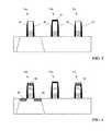
- FIG. 1shows a cross-section view of a semiconductor structure comprising a substrate 10 including an active region 13 and an isolation region 15 .
- the substrate 10may comprise any suitable semiconductor substrate including, but not limited to: Si, SiGe, SiC, SiGeC, and layered semiconductors such as silicon-on-insulator (SOI), Si/SiGe, and SiGe-on-insulator (SGOI).
- SOIsilicon-on-insulator
- Si/SiGeSi/SiGe
- SGOISiGe-on-insulator
- a gate dielectric 20is formed on portions of the substrate 10 .
- the gate dielectric 20comprises a high-k gate dielectric such as a layer of hafnium oxide formed on the substrate 10 .
- the gate dielectric 20 layermay have a depth (e.g., thickness) of about 1 nm to about to 2 nm, while other thicknesses are also contemplated by the present invention.
- the gate dielectric 20has a dielectric constant value of about 15.0 or greater, which is considered high-k.
- the inventionis not limited to this particular arrangement of gate dielectric and any suitable material or layers of materials may be used as the gate dielectric 20 in accordance with aspects of the invention.
- the gate dielectric 20may be composed of hafnium silicate or other hafnium-based or zirconium-based high-k materials.
- the gate dielectric 20may be formed using conventional deposition process such as, for example, chemical vapor deposition (CVD) or plasma-assisted CVD, or a thermal growing process such as oxidation, nitridation or oxynitridation.
- a metal layer 30is formed on the gate dielectric 20 .
- the metal layer 30(e.g., gate metal layer) may be composed of any suitable gate electrode material such as, for example, titanium nitride (TiN), titanium tantalum nitride (TiTaN), other metals containing at least one of titanium, tantalum, and tungsten, or any other suitable conductive material.
- the metal layer 30may have a depth of about 3 nm to about 8 nm, or any other desired depth (e.g., thickness), and may be formed using conventional techniques, e.g., chemical vapor deposition (CVD).
- a silicon layer 40is formed on the metal layer 30 .
- the silicon layer 40has a thickness of about 5 nm to about 20 nm; however, the invention is not limited to these thicknesses and any suitable thickness may be used within the scope of the invention.
- the silicon layer 40is formed by a physical vapor deposition (PVD) process, but may also be formed by other processes, such as chemical vapor deposition (CVD).
- FIG. 1also shows an etch-stop layer 50 formed on the silicon layer 40 .
- the etch-stop layer 50may be composed of materials including, but not limited to, silicon dioxide, silicon oxynitride, and other oxides.
- the etch-stop layer 50may also be composed of a high-k dielectric, such as those described with respect to gate dielectric 20 .
- the etch-stop layerhas a thickness of about 2 nm to about 5 nm; however, the invention is not limited to these thicknesses and any suitable thickness may be used within the scope of the invention.
- the etch-stop layer 50may be formed using conventional deposition process such as, for example, chemical vapor deposition (CVD) or plasma-assisted CVD, or a thermal growing process such as oxidation, nitridation or oxynitridation.
- CVDchemical vapor deposition
- plasma-assisted CVDplasma-assisted CVD
- thermal growing processsuch as oxidation, nitridation or oxynitridation.
- a polysilicon layer 60is formed on the etch-stop layer 50 .
- the polysilicon layer 60has a thickness of about 50 nm to about 80 nm; however, the invention is not limited to these thicknesses and any suitable thickness may be used within the scope of the invention.
- the polysilicon layer 60may be formed using any suitable technique including, but not limited to, chemical vapor deposition (CVD).
- the layers 20 , 30 , 40 , 50 , and 60are patterned into stacks 70 a , 70 b , 70 c .
- the patterningmay be performed using any conventional patterning process, such as, for example, photolithographic masking and reactive ion etch (RIE).
- RIEreactive ion etch
- three stacks 70 a - care shown, the invention is not limited to this number, and any desired number of stacks may be formed from the polysilicon layer 60 .
- at least one stacke.g., stack 70 a
- at least one other stacke.g., stacks 70 b and 70 c
- stacks formed over an active regioncorrespond to a transistor and stacks over an isolation region correspond to a passive device, e.g., a resistor, e-fuse, etc.
- stack 70 acorresponds to a transistor 72 (e.g., FET)
- stack 70 bcorresponds to a resistor 73
- stack 70 ccorresponds to an e-fuse 74 ; however, the invention is not limited to this particular configuration and any desired configuration of stacks may be used.
- the stack 70 aincludes a dummy gate 77 a of the transistor 72 formed from the polysilicon layer 60 , and the stacks 70 b and 70 c comprise polysilicon features 77 b and 77 c formed from the same polysilicon layer 60 .
- FIG. 3shows the formation of sidewall spacers 80 adjacent the sides of the stacks 70 a - c .
- the sidewall spacers 80may be formed using conventional techniques, such as for example, blanket deposition of SiN via CVD, masking, and RIE.
- the sidewall spacers 80may comprise any suitable materials, such as, for example, SiN, SiO 2 , etc.
- a cap 85may be provided on the stack 70 b .
- the cap 85may be formed from the same material as the sidewall spacers 80 (e.g., SiN) and may be formed from the same initial blanket deposition of spacer material via appropriate masking.
- any suitable transistor featuressuch as implants (e.g., source, drain, halo, junction, etc.), embedded silicon germanium (eSiGe) source/drain, etc., may be formed with the structure of FIG. 3 using conventional semiconductor fabrication techniques.
- implantse.g., source, drain, halo, junction, etc.
- eSiGeembedded silicon germanium
- silicide regions 90may be formed on exposed areas of silicon, including source/drain regions adjacent stack 70 a , atop dummy gate 77 a , and atop polysilicon feature 77 c .
- the silicide regions 90may be formed in any suitable manner.
- the silicide regions 90may be formed by selectively sputtering a nickel film onto the exposed silicon and annealing the film to form nickel silicide (NiSi).
- the silicidehas a thickness of about 15 nm to 30 nm, although other thicknesses may be used within the scope of the invention.
- the inventionis not limited to NiSi, and other silicides, such as cobalt silicide, may be used.
- a barrier layer 100is conformally deposited over the entire structure including portions of the substrate 10 .
- the barrier layer 100may be composed of, for example, SiN and may be formed in any conventional manner, e.g., plasma enhanced chemical vapor deposition (PECVD), etc.
- PECVDplasma enhanced chemical vapor deposition
- the barrier layer 100may comprise a first portion that is arranged in tensile stress formed over a NFET device and a second portion arranged in compressive stress formed over a PFET device. Dual stress liners and their fabrication are known such that further explanation is not believed necessary.
- a dielectric layer 110is deposited over the entire structure and the resulting structure is planarized.
- the dielectric layer 110may be composed of any suitable material including but limited to SiO 2 , tetraethylorthosilicate (TEOS), borophosphosilicate glass (BPSG), etc., and may be formed in any conventional manner, e.g., PECVD, etc.
- the dielectric layer 110is planarized down to the barrier layer 100 atop the stacks 70 a - c .
- the planarizationmay be performed using any suitable technique, including but not limited to chemical mechanical polishing (CMP).
- CMPchemical mechanical polishing
- the planarizationmay remove some, but not all, of the barrier layer 100 from atop the stacks 70 a - c.
- a photoresist mask 120is deposited and patterned (e.g., exposed and developed) on the upper surface of the structure.
- the photoresist mask 120is deposited and patterned using conventional lithographic materials and etching processes.
- the pattern formed in the photoresist mask 120covers the stacks that correspond to the resistor 73 and e-fuse 74 while leaving the stack corresponding to the transistor 72 unmasked.
- FIG. 8shows the removal of a portion of the barrier layer 100 from over the stack 70 a exposing the silicide region 90 .
- the portion of the barrier layer 100is removed using a dry RIE process; however, any suitable process can be used within the scope of the invention.
- the photoresist mask 120protects the other devices (e.g., stacks 70 b and 70 c ) while the portion of the barrier layer 100 is removed from over the transistor stack 70 a .
- the portion of the barrier layer 100is removed from over the transistor stack 70 a without removing any of the barrier layer 100 over the other devices (e.g., stacks 70 b and 70 c ).
- the photoresist mask 120is stripped from atop the dielectric 110 and the barrier layer 100 using conventional mask stripping processes.
- the silicide region 90 atop the dummy gate 77 ais removed.
- the silicide region 90is removed using a wet bath of hydrofluoric acid (HF); however, any suitable process may be used within the scope of the invention.
- FIGS. 9 and 10depict stripping the photoresist mask 120 before removing the silicide region 90 , it is understood that the order of these two steps can be reversed.
- the other devicese.g., stacks 70 b and 70 c
- the other devicesare protected by the barrier layer 100 while the transistor 72 undergoes further processing as described herein.
- the dummy gate 77 ais removed, as shown in FIG. 11 .
- the removal of the dummy gate 77 amay be considered a selective removal since the other devices (e.g., stacks 70 b and 70 c ) are protected (e.g., masked) by the barrier layer 100 during removal of the dummy gate 77 a .
- the dummy gate 77 ais removed without affecting the stacks 70 b and 70 c including the polysilicon features 77 b and 77 c .
- the polysilicon of the dummy gate 77 ais etched using a wet ammonium hydroxide (NH 4 OH) etch process.
- NH 4 OHwet ammonium hydroxide
- the inventionis not limited to this etch process, and other suitable processes may be used including, but not limited to, a chlorine-based or a bromine-based dry etch.
- the etch-stop layer 50halts the etch during removal of the dummy gate 77 a and protects the underlying silicon layer 40 .
- the etch-stop layer 50is removed from the transistor.
- a wet HF processis used to remove the etch-stop layer 50 ; however, the invention is not limited to this process and ay suitable process may be used. Removal of the etch-stop layer 50 exposes the silicon layer 40 in the transistor 72 .
- a silicide gate contact 130is formed at the transistor 72 .
- the silicide gate contact 130is formed by depositing a thin (e.g., about 2 nm to about 10 nm) film of nickel on the silicon layer 40 of the transistor and then thermally annealing the device to create NiSi atop the metal layer 30 of the transistor.
- Semiconductor fabrication techniques for forming silicideare known such that further explanation is not believed necessary.
- a metal gate 140 for the transistoris formed on the high-k dielectric 20 , the metal gate 140 having a height of about 10 nm to about 30 nm.
- the metal gate 140 of the transistormay be formed at less than half the height of the polysilicon features 77 b and 77 c associated with the resistor and e-fuse, which reduces overall system capacitance without negatively affecting the performance of the resistor and/or e-fuse.
- a dielectric material 150is formed in the gate trench, after which standard semiconductor processing steps may be used to form contacts to the operative portions of the transistor, resistor, and e-fuse.
- a metal gate of a transistoris formed on a high-k dielectric using a damascene gate approach.
- the metal gateis formed using a dummy gate that is patterned from a same silicon layer as a polysilicon feature for another device, such as a resistor and/or an e-fuse.
- a maskis used to protect the other device during removal of the dummy gate.
- the gate height of the metal gatemay be aggressively scaled to as low as about 10 nm to about 30 nm while the polysilicon feature height of the other device remains on the order of about 50 nm to about 80 nm, which advantageously reduces overall system capacitance without negatively affecting the performance of the resistor and/or e-fuse. Since the dummy gate is formed from the same polysilicon layer as the polysilicon feature of the other device, implementations of the invention avoid multiple polysilicon depositions that can lead to interference in the gate stack.
- FIG. 15shows a block diagram of an exemplary design flow 900 used for example, in semiconductor IC logic design, simulation, test, layout, and manufacture.
- Design flow 900includes processes, machines and/or mechanisms for processing design structures or devices to generate logically or otherwise functionally equivalent representations of the design structures and/or devices described above and shown in FIGS. 1-14 .
- the design structures processed and/or generated by design flow 900may be encoded on machine-readable transmission or storage media to include data and/or instructions that when executed or otherwise processed on a data processing system generate a logically, structurally, mechanically, or otherwise functionally equivalent representation of hardware components, circuits, devices, or systems.
- Machinesinclude, but are not limited to, any machine used in an IC design process, such as designing, manufacturing, or simulating a circuit, component, device, or system.
- machinesmay include: lithography machines, machines and/or equipment for generating masks (e.g. e-beam writers), computers or equipment for simulating design structures, any apparatus used in the manufacturing or test process, or any machines for programming functionally equivalent representations of the design structures into any medium (e.g. a machine for programming a programmable gate array).
- Design flow 900may vary depending on the type of representation being designed. For example, a design flow 900 for building an application specific IC (ASIC) may differ from a design flow 900 for designing a standard component or from a design flow 900 for instantiating the design into a programmable array, for example a programmable gate array (PGA) or a field programmable gate array (FPGA).
- ASICapplication specific IC
- PGAprogrammable gate array
- FPGAfield programmable gate array
- FIG. 15illustrates multiple such design structures including an input design structure 920 that is preferably processed by a design process 910 .
- Design structure 920may be a logical simulation design structure generated and processed by design process 910 to produce a logically equivalent functional representation of a hardware device.
- Design structure 920may also or alternatively comprise data and/or program instructions that when processed by design process 910 , generate a functional representation of the physical structure of a hardware device. Whether representing functional and/or structural design features, design structure 920 may be generated using electronic computer-aided design (ECAD) such as implemented by a core developer/designer.
- ECADelectronic computer-aided design
- design structure 920When encoded on a machine-readable data transmission, gate array, or storage medium, design structure 920 may be accessed and processed by one or more hardware and/or software modules within design process 910 to simulate or otherwise functionally represent an electronic component, circuit, electronic or logic module, apparatus, device, or system such as those shown in FIGS. 1-14 .
- design structure 920may comprise files or other data structures including human and/or machine-readable source code, compiled structures, and computer-executable code structures that when processed by a design or simulation data processing system, functionally simulate or otherwise represent circuits or other levels of hardware logic design.
- Such data structuresmay include hardware-description language (HDL) design entities or other data structures conforming to and/or compatible with lower-level HDL design languages such as Verilog and VHDL, and/or higher level design languages such as C or C++.
- HDLhardware-description language
- Design process 910preferably employs and incorporates hardware and/or software modules for synthesizing, translating, or otherwise processing a design/simulation functional equivalent of the components, circuits, devices, or logic structures shown in FIGS. 1-14 to generate a netlist 980 which may contain design structures such as design structure 920 .
- Netlist 980may comprise, for example, compiled or otherwise processed data structures representing a list of wires, discrete components, logic gates, control circuits, I/O devices, models, etc. that describes the connections to other elements and circuits in an integrated circuit design.
- Netlist 980may be synthesized using an iterative process in which netlist 980 is resynthesized one or more times depending on design specifications and parameters for the device.
- netlist 980may be recorded on a machine-readable data storage medium or programmed into a programmable gate array.
- the mediummay be a non-volatile storage medium such as a magnetic or optical disk drive, a programmable gate array, a compact flash, or other flash memory. Additionally, or in the alternative, the medium may be a system or cache memory, buffer space, or electrically or optically conductive devices and materials on which data packets may be transmitted and intermediately stored via the Internet, or other networking suitable means.
- Design process 910may include hardware and software modules for processing a variety of input data structure types including netlist 980 .
- data structure typesmay reside, for example, within library elements 930 and include a set of commonly used elements, circuits, and devices, including models, layouts, and symbolic representations, for a given manufacturing technology (e.g., different technology nodes, 32 nm, 45 nm, 90 nm, etc.).
- the data structure typesmay further include design specifications 940 , characterization data 950 , verification data 960 , design rules 970 , and test data files 985 which may include input test patterns, output test results, and other testing information.
- Design process 910may further include, for example, standard mechanical design processes such as stress analysis, thermal analysis, mechanical event simulation, process simulation for operations such as casting, molding, and die press forming, etc.
- standard mechanical design processessuch as stress analysis, thermal analysis, mechanical event simulation, process simulation for operations such as casting, molding, and die press forming, etc.
- One of ordinary skill in the art of mechanical designcan appreciate the extent of possible mechanical design tools and applications used in design process 910 without deviating from the scope and spirit of the invention.
- Design process 910may also include modules for performing standard circuit design processes such as timing analysis, verification, design rule checking, place and route operations, etc.
- Design process 910employs and incorporates logic and physical design tools such as HDL compilers and simulation model build tools to process design structure 920 together with some or all of the depicted supporting data structures along with any additional mechanical design or data (if applicable), to generate a second design structure 990 .
- Design structure 990resides on a storage medium or programmable gate array in a data format used for the exchange of data of mechanical devices and structures (e.g. information stored in a IGES, DXF, Parasolid XT, JT, DRG, or any other suitable format for storing or rendering such mechanical design structures).
- design structure 990preferably comprises one or more files, data structures, or other computer-encoded data or instructions that reside on transmission or data storage media and that when processed by an ECAD system generate a logically or otherwise functionally equivalent form of one or more of the embodiments of the invention shown in FIGS. 1-14 .
- design structure 990may comprise a compiled, executable HDL simulation model that functionally simulates the devices shown in FIGS. 1-14 .
- Design structure 990may also employ a data format used for the exchange of layout data of integrated circuits and/or symbolic data format (e.g. information stored in a GDSII (GDS2), GL1, OASIS, map files, or any other suitable format for storing such design data structures).
- Design structure 990may comprise information such as, for example, symbolic data, map files, test data files, design content files, manufacturing data, layout parameters, wires, levels of metal, vias, shapes, data for routing through the manufacturing line, and any other data required by a manufacturer or other designer/developer to produce a device or structure as described above and shown in FIGS. 1-14 .
- Design structure 990may then proceed to a stage 995 where, for example, design structure 990 : proceeds to tape-out, is released to manufacturing, is released to a mask house, is sent to another design house, is sent back to the customer, etc.
- the method as described aboveis used in the fabrication of integrated circuit chips.
- the resulting integrated circuit chipscan be distributed by the fabricator in raw wafer form (that is, as a single wafer that has multiple unpackaged chips), as a bare die, or in a packaged form.
- the chipis mounted in a single chip package (such as a plastic carrier, with leads that are affixed to a motherboard or other higher level carrier) or in a multichip package (such as a ceramic carrier that has either or both surface interconnections or buried interconnections).
- the chipis then integrated with other chips, discrete circuit elements, and/or other signal processing devices as part of either (a) an intermediate product, such as a motherboard, or (b) an end product.
- the end productcan be any product that includes integrated circuit chips, ranging from toys and other low-end applications to advanced computer products having a display, a keyboard or other input device, and a central processor.
Landscapes
- Design And Manufacture Of Integrated Circuits (AREA)
- Semiconductor Integrated Circuits (AREA)
- Metal-Oxide And Bipolar Metal-Oxide Semiconductor Integrated Circuits (AREA)
Abstract
Description
Claims (16)
Priority Applications (2)
| Application Number | Priority Date | Filing Date | Title |
|---|---|---|---|
| US12/715,781US8138037B2 (en) | 2009-03-17 | 2010-03-02 | Method and structure for gate height scaling with high-k/metal gate technology |
| US13/364,564US8227870B2 (en) | 2009-03-17 | 2012-02-02 | Method and structure for gate height scaling with high-k/metal gate technology |
Applications Claiming Priority (2)
| Application Number | Priority Date | Filing Date | Title |
|---|---|---|---|
| US16086709P | 2009-03-17 | 2009-03-17 | |
| US12/715,781US8138037B2 (en) | 2009-03-17 | 2010-03-02 | Method and structure for gate height scaling with high-k/metal gate technology |
Related Child Applications (1)
| Application Number | Title | Priority Date | Filing Date |
|---|---|---|---|
| US13/364,564DivisionUS8227870B2 (en) | 2009-03-17 | 2012-02-02 | Method and structure for gate height scaling with high-k/metal gate technology |
Publications (2)
| Publication Number | Publication Date |
|---|---|
| US20100237435A1 US20100237435A1 (en) | 2010-09-23 |
| US8138037B2true US8138037B2 (en) | 2012-03-20 |
Family
ID=42736777
Family Applications (2)
| Application Number | Title | Priority Date | Filing Date |
|---|---|---|---|
| US12/715,781Expired - Fee RelatedUS8138037B2 (en) | 2009-03-17 | 2010-03-02 | Method and structure for gate height scaling with high-k/metal gate technology |
| US13/364,564Expired - Fee RelatedUS8227870B2 (en) | 2009-03-17 | 2012-02-02 | Method and structure for gate height scaling with high-k/metal gate technology |
Family Applications After (1)
| Application Number | Title | Priority Date | Filing Date |
|---|---|---|---|
| US13/364,564Expired - Fee RelatedUS8227870B2 (en) | 2009-03-17 | 2012-02-02 | Method and structure for gate height scaling with high-k/metal gate technology |
Country Status (1)
| Country | Link |
|---|---|
| US (2) | US8138037B2 (en) |
Cited By (38)
| Publication number | Priority date | Publication date | Assignee | Title |
|---|---|---|---|---|
| US20120129312A1 (en)* | 2010-11-22 | 2012-05-24 | International Business Machines Corporation | Method of forming e-fuse in replacement metal gate manufacturing process |
| US20120292739A1 (en)* | 2011-05-18 | 2012-11-22 | Taiwan Semiconductor Manufacturing Company, Ltd. | Integrated circuit having silicon resistor and method of forming the same |
| US8574987B1 (en)* | 2012-06-08 | 2013-11-05 | Freescale Semiconductor, Inc. | Integrating formation of a replacement gate transistor and a non-volatile memory cell using an interlayer dielectric |
| US8658497B2 (en) | 2012-01-04 | 2014-02-25 | Freescale Semiconductor, Inc. | Non-volatile memory (NVM) and logic integration |
| US8669158B2 (en) | 2012-01-04 | 2014-03-11 | Mark D. Hall | Non-volatile memory (NVM) and logic integration |
| US8716089B1 (en) | 2013-03-08 | 2014-05-06 | Freescale Semiconductor, Inc. | Integrating formation of a replacement gate transistor and a non-volatile memory cell having thin film storage |
| US8716781B2 (en) | 2012-04-09 | 2014-05-06 | Freescale Semiconductor, Inc. | Logic transistor and non-volatile memory cell integration |
| US8728886B2 (en) | 2012-06-08 | 2014-05-20 | Freescale Semiconductor, Inc. | Integrating formation of a replacement gate transistor and a non-volatile memory cell using a high-k dielectric |
| US8741719B1 (en) | 2013-03-08 | 2014-06-03 | Freescale Semiconductor, Inc. | Integrating formation of a logic transistor and a non-volatile memory cell using a partial replacement gate technique |
| US8871598B1 (en) | 2013-07-31 | 2014-10-28 | Freescale Semiconductor, Inc. | Non-volatile memory (NVM) and high-k and metal gate integration using gate-first methodology |
| US8877585B1 (en) | 2013-08-16 | 2014-11-04 | Freescale Semiconductor, Inc. | Non-volatile memory (NVM) cell, high voltage transistor, and high-K and metal gate transistor integration |
| US8878337B1 (en)* | 2011-07-19 | 2014-11-04 | Xilinx, Inc. | Integrated circuit structure having a capacitor structured to reduce dishing of metal layers |
| US8877568B2 (en) | 2010-10-29 | 2014-11-04 | Freescale Semiconductor, Inc. | Methods of making logic transistors and non-volatile memory cells |
| US8901632B1 (en) | 2013-09-30 | 2014-12-02 | Freescale Semiconductor, Inc. | Non-volatile memory (NVM) and high-K and metal gate integration using gate-last methodology |
| US8906764B2 (en) | 2012-01-04 | 2014-12-09 | Freescale Semiconductor, Inc. | Non-volatile memory (NVM) and logic integration |
| US8932925B1 (en) | 2013-08-22 | 2015-01-13 | Freescale Semiconductor, Inc. | Split-gate non-volatile memory (NVM) cell and device structure integration |
| US8951863B2 (en) | 2012-04-06 | 2015-02-10 | Freescale Semiconductor, Inc. | Non-volatile memory (NVM) and logic integration |
| US9006093B2 (en) | 2013-06-27 | 2015-04-14 | Freescale Semiconductor, Inc. | Non-volatile memory (NVM) and high voltage transistor integration |
| US9041076B2 (en) | 2013-02-03 | 2015-05-26 | International Business Machines Corporation | Partial sacrificial dummy gate with CMOS device with high-k metal gate |
| US9082650B2 (en) | 2013-08-21 | 2015-07-14 | Freescale Semiconductor, Inc. | Integrated split gate non-volatile memory cell and logic structure |
| US9082837B2 (en) | 2013-08-08 | 2015-07-14 | Freescale Semiconductor, Inc. | Nonvolatile memory bitcell with inlaid high k metal select gate |
| US9087913B2 (en) | 2012-04-09 | 2015-07-21 | Freescale Semiconductor, Inc. | Integration technique using thermal oxide select gate dielectric for select gate and apartial replacement gate for logic |
| US9111865B2 (en) | 2012-10-26 | 2015-08-18 | Freescale Semiconductor, Inc. | Method of making a logic transistor and a non-volatile memory (NVM) cell |
| US9112056B1 (en) | 2014-03-28 | 2015-08-18 | Freescale Semiconductor, Inc. | Method for forming a split-gate device |
| US9129996B2 (en) | 2013-07-31 | 2015-09-08 | Freescale Semiconductor, Inc. | Non-volatile memory (NVM) cell and high-K and metal gate transistor integration |
| US9129855B2 (en) | 2013-09-30 | 2015-09-08 | Freescale Semiconductor, Inc. | Non-volatile memory (NVM) and high-k and metal gate integration using gate-first methodology |
| US9136129B2 (en) | 2013-09-30 | 2015-09-15 | Freescale Semiconductor, Inc. | Non-volatile memory (NVM) and high-k and metal gate integration using gate-last methodology |
| US9231077B2 (en) | 2014-03-03 | 2016-01-05 | Freescale Semiconductor, Inc. | Method of making a logic transistor and non-volatile memory (NVM) cell |
| US9252152B2 (en) | 2014-03-28 | 2016-02-02 | Freescale Semiconductor, Inc. | Method for forming a split-gate device |
| US9252246B2 (en) | 2013-08-21 | 2016-02-02 | Freescale Semiconductor, Inc. | Integrated split gate non-volatile memory cell and logic device |
| US9257445B2 (en) | 2014-05-30 | 2016-02-09 | Freescale Semiconductor, Inc. | Method of making a split gate non-volatile memory (NVM) cell and a logic transistor |
| US9275864B2 (en) | 2013-08-22 | 2016-03-01 | Freescale Semiconductor,Inc. | Method to form a polysilicon nanocrystal thin film storage bitcell within a high k metal gate platform technology using a gate last process to form transistor gates |
| US9343314B2 (en) | 2014-05-30 | 2016-05-17 | Freescale Semiconductor, Inc. | Split gate nanocrystal memory integration |
| US9379222B2 (en) | 2014-05-30 | 2016-06-28 | Freescale Semiconductor, Inc. | Method of making a split gate non-volatile memory (NVM) cell |
| US9472418B2 (en) | 2014-03-28 | 2016-10-18 | Freescale Semiconductor, Inc. | Method for forming a split-gate device |
| TWI825557B (en)* | 2021-10-22 | 2023-12-11 | 南亞科技股份有限公司 | Fuse component, semiconductor device, and method for manufacturing a fuse component |
| US11916015B2 (en) | 2021-10-26 | 2024-02-27 | Nanya Technology Corporation | Fuse component, semiconductor device, and method for manufacturing a fuse component |
| US12057393B2 (en) | 2021-10-22 | 2024-08-06 | Nanya Technology Corporation | Semiconductor device with fuse component |
Families Citing this family (31)
| Publication number | Priority date | Publication date | Assignee | Title |
|---|---|---|---|---|
| US8890260B2 (en)* | 2009-09-04 | 2014-11-18 | Taiwan Semiconductor Manufacturing Company, Ltd. | Polysilicon design for replacement gate technology |
| US8071437B2 (en)* | 2009-11-19 | 2011-12-06 | United Microelectronics Corp. | Method of fabricating efuse, resistor and transistor |
| US20110198705A1 (en)* | 2010-02-18 | 2011-08-18 | Broadcom Corporation | Integrated resistor using gate metal for a resistive element |
| US8697517B2 (en) | 2010-03-16 | 2014-04-15 | Taiwan Semiconductor Manufacturing Company, Ltd. | Reduced substrate coupling for inductors in semiconductor devices |
| DE102010003559B4 (en)* | 2010-03-31 | 2019-07-18 | Globalfoundries Dresden Module One Llc & Co. Kg | Semiconductor device having metal gate structures made by an exchange gate method and e-fuse having a silicide |
| US8980753B2 (en)* | 2010-09-21 | 2015-03-17 | United Mircroelectronics Corp. | Metal gate transistor and method for fabricating the same |
| CN102544089B (en)* | 2010-12-08 | 2015-06-17 | 中国科学院微电子研究所 | Semiconductor device and method for manufacturing the same |
| US20120244693A1 (en)* | 2011-03-22 | 2012-09-27 | Tokyo Electron Limited | Method for patterning a full metal gate structure |
| US8367494B2 (en)* | 2011-04-05 | 2013-02-05 | International Business Machines Corporation | Electrical fuse formed by replacement metal gate process |
| US8629007B2 (en) | 2011-07-14 | 2014-01-14 | International Business Machines Corporation | Method of improving replacement metal gate fill |
| DE102011080439B4 (en)* | 2011-08-04 | 2018-11-15 | Globalfoundries Inc. | Semiconductor device and method for manufacturing a semiconductor device |
| TWI569332B (en)* | 2011-10-06 | 2017-02-01 | 聯華電子股份有限公司 | Semiconductor device and fabrication method thereof |
| US8633549B2 (en) | 2011-10-06 | 2014-01-21 | United Microelectronics Corp. | Semiconductor device and fabrication method thereof |
| US9524934B2 (en)* | 2011-11-22 | 2016-12-20 | Taiwan Semiconductor Manufacturing Company, Ltd. | Integrated circuits with electrical fuses and methods of forming the same |
| CN103390583B (en)* | 2012-05-08 | 2015-12-16 | 中芯国际集成电路制造(上海)有限公司 | Semiconductor integrated device and preparation method thereof |
| US9076818B2 (en)* | 2012-06-20 | 2015-07-07 | GlobalFoundries, Inc. | Semiconductor device fabrication methods |
| US8796772B2 (en)* | 2012-09-24 | 2014-08-05 | Intel Corporation | Precision resistor for non-planar semiconductor device architecture |
| US9219059B2 (en) | 2012-09-26 | 2015-12-22 | International Business Machines Corporation | Semiconductor structure with integrated passive structures |
| US8835237B2 (en)* | 2012-11-07 | 2014-09-16 | International Business Machines Corporation | Robust replacement gate integration |
| CN103839808B (en)* | 2012-11-21 | 2017-11-21 | 中国科学院微电子研究所 | Semiconductor device manufacturing method |
| CN103915323B (en)* | 2013-01-08 | 2016-08-31 | 中芯国际集成电路制造(上海)有限公司 | The preparation method of transistor |
| CN103295889B (en)* | 2013-05-28 | 2016-03-02 | 上海华力微电子有限公司 | Fin-shaped active area is prepared the method for high-K metal gate |
| CN105225949B (en)* | 2014-05-26 | 2018-08-21 | 中芯国际集成电路制造(上海)有限公司 | A kind of manufacturing method and electronic device of semiconductor devices |
| US9583400B1 (en) | 2016-01-15 | 2017-02-28 | International Business Machines Corporation | Gate stack with tunable work function |
| US9559016B1 (en) | 2016-01-15 | 2017-01-31 | International Business Machines Corporation | Semiconductor device having a gate stack with tunable work function |
| US9991167B2 (en)* | 2016-03-30 | 2018-06-05 | Globalfoundries Inc. | Method and IC structure for increasing pitch between gates |
| US10411091B1 (en) | 2018-07-13 | 2019-09-10 | Qualcomm Incorporated | Integrated circuits employing a field gate(s) without dielectric layers and/or work function metal layers for reduced gate layout parasitic resistance, and related methods |
| US12002752B2 (en) | 2021-12-03 | 2024-06-04 | Nanya Technology Corporation | Method for manufacturing a fuse component |
| TWI817349B (en)* | 2021-12-03 | 2023-10-01 | 南亞科技股份有限公司 | Fuse component and semiconductor device |
| US12308315B2 (en) | 2021-12-06 | 2025-05-20 | Nanya Technology Corporation | Fuse component and semiconductor device |
| CN118574509B (en)* | 2024-08-05 | 2024-11-29 | 武汉新芯集成电路股份有限公司 | Semiconductor device and manufacturing method thereof |
Citations (9)
| Publication number | Priority date | Publication date | Assignee | Title |
|---|---|---|---|---|
| US6333223B1 (en)* | 1998-12-25 | 2001-12-25 | Matsushita Electric Industrial Co., Ltd. | Semiconductor device and method of manufacturing the same |
| US20080038879A1 (en) | 2004-05-06 | 2008-02-14 | Sidense Corporation | Split-channel antifuse array architecture |
| US7534671B2 (en) | 2006-03-23 | 2009-05-19 | Taiwan Semiconductor Manufacturing Co., Ltd. | Method for integrally forming an electrical fuse device and a MOS transistor |
| US20090236669A1 (en) | 2008-03-20 | 2009-09-24 | Yi-Wen Chen | Metal gate transistor and polysilicon resistor and method for fabricating the same |
| US20090283840A1 (en) | 2008-05-13 | 2009-11-19 | International Business Machines Corporation | Metal gate integration structure and method including metal fuse, anti-fuse and/or resistor |
| US20100019344A1 (en) | 2008-07-25 | 2010-01-28 | Taiwan Semiconductor Manufacturing Company, Ltd. | Novel poly resistor and poly efuse design for replacement gate technology |
| US20100052058A1 (en) | 2008-08-29 | 2010-03-04 | Taiwan Semiconductor Manufacturing Company, Ltd. | Downsize polysilicon height for polysilicon resistor integration of replacement gate process |
| US20100059823A1 (en) | 2008-09-10 | 2010-03-11 | Taiwan Semiconductor Manufacturing Company, Ltd. | Resistive device for high-k metal gate technology and method of making |
| US20100087055A1 (en) | 2008-10-06 | 2010-04-08 | Taiwan Semiconductor Manufacturing Company, Ltd. | Method for gate height control in a gate last process |
- 2010
- 2010-03-02USUS12/715,781patent/US8138037B2/ennot_activeExpired - Fee Related
- 2012
- 2012-02-02USUS13/364,564patent/US8227870B2/ennot_activeExpired - Fee Related
Patent Citations (9)
| Publication number | Priority date | Publication date | Assignee | Title |
|---|---|---|---|---|
| US6333223B1 (en)* | 1998-12-25 | 2001-12-25 | Matsushita Electric Industrial Co., Ltd. | Semiconductor device and method of manufacturing the same |
| US20080038879A1 (en) | 2004-05-06 | 2008-02-14 | Sidense Corporation | Split-channel antifuse array architecture |
| US7534671B2 (en) | 2006-03-23 | 2009-05-19 | Taiwan Semiconductor Manufacturing Co., Ltd. | Method for integrally forming an electrical fuse device and a MOS transistor |
| US20090236669A1 (en) | 2008-03-20 | 2009-09-24 | Yi-Wen Chen | Metal gate transistor and polysilicon resistor and method for fabricating the same |
| US20090283840A1 (en) | 2008-05-13 | 2009-11-19 | International Business Machines Corporation | Metal gate integration structure and method including metal fuse, anti-fuse and/or resistor |
| US20100019344A1 (en) | 2008-07-25 | 2010-01-28 | Taiwan Semiconductor Manufacturing Company, Ltd. | Novel poly resistor and poly efuse design for replacement gate technology |
| US20100052058A1 (en) | 2008-08-29 | 2010-03-04 | Taiwan Semiconductor Manufacturing Company, Ltd. | Downsize polysilicon height for polysilicon resistor integration of replacement gate process |
| US20100059823A1 (en) | 2008-09-10 | 2010-03-11 | Taiwan Semiconductor Manufacturing Company, Ltd. | Resistive device for high-k metal gate technology and method of making |
| US20100087055A1 (en) | 2008-10-06 | 2010-04-08 | Taiwan Semiconductor Manufacturing Company, Ltd. | Method for gate height control in a gate last process |
Cited By (43)
| Publication number | Priority date | Publication date | Assignee | Title |
|---|---|---|---|---|
| US8877568B2 (en) | 2010-10-29 | 2014-11-04 | Freescale Semiconductor, Inc. | Methods of making logic transistors and non-volatile memory cells |
| US8492286B2 (en)* | 2010-11-22 | 2013-07-23 | International Business Machines Corporation | Method of forming E-fuse in replacement metal gate manufacturing process |
| US20120129312A1 (en)* | 2010-11-22 | 2012-05-24 | International Business Machines Corporation | Method of forming e-fuse in replacement metal gate manufacturing process |
| US20120292739A1 (en)* | 2011-05-18 | 2012-11-22 | Taiwan Semiconductor Manufacturing Company, Ltd. | Integrated circuit having silicon resistor and method of forming the same |
| US8563389B2 (en)* | 2011-05-18 | 2013-10-22 | Taiwan Semiconductor Manufacturing Company, Ltd. | Integrated circuit having silicon resistor and method of forming the same |
| US8878337B1 (en)* | 2011-07-19 | 2014-11-04 | Xilinx, Inc. | Integrated circuit structure having a capacitor structured to reduce dishing of metal layers |
| US8658497B2 (en) | 2012-01-04 | 2014-02-25 | Freescale Semiconductor, Inc. | Non-volatile memory (NVM) and logic integration |
| US8906764B2 (en) | 2012-01-04 | 2014-12-09 | Freescale Semiconductor, Inc. | Non-volatile memory (NVM) and logic integration |
| US8669158B2 (en) | 2012-01-04 | 2014-03-11 | Mark D. Hall | Non-volatile memory (NVM) and logic integration |
| US8951863B2 (en) | 2012-04-06 | 2015-02-10 | Freescale Semiconductor, Inc. | Non-volatile memory (NVM) and logic integration |
| US8716781B2 (en) | 2012-04-09 | 2014-05-06 | Freescale Semiconductor, Inc. | Logic transistor and non-volatile memory cell integration |
| US8722493B2 (en) | 2012-04-09 | 2014-05-13 | Freescale Semiconductor, Inc. | Logic transistor and non-volatile memory cell integration |
| US9087913B2 (en) | 2012-04-09 | 2015-07-21 | Freescale Semiconductor, Inc. | Integration technique using thermal oxide select gate dielectric for select gate and apartial replacement gate for logic |
| US8728886B2 (en) | 2012-06-08 | 2014-05-20 | Freescale Semiconductor, Inc. | Integrating formation of a replacement gate transistor and a non-volatile memory cell using a high-k dielectric |
| US8574987B1 (en)* | 2012-06-08 | 2013-11-05 | Freescale Semiconductor, Inc. | Integrating formation of a replacement gate transistor and a non-volatile memory cell using an interlayer dielectric |
| US9111865B2 (en) | 2012-10-26 | 2015-08-18 | Freescale Semiconductor, Inc. | Method of making a logic transistor and a non-volatile memory (NVM) cell |
| US9299795B2 (en) | 2012-10-28 | 2016-03-29 | International Business Machines Corporation | Partial sacrificial dummy gate with CMOS device with high-k metal gate |
| US9853116B2 (en) | 2012-10-28 | 2017-12-26 | International Business Machines Corporation | Partial sacrificial dummy gate with CMOS device with high-k metal gate |
| US9041076B2 (en) | 2013-02-03 | 2015-05-26 | International Business Machines Corporation | Partial sacrificial dummy gate with CMOS device with high-k metal gate |
| US8716089B1 (en) | 2013-03-08 | 2014-05-06 | Freescale Semiconductor, Inc. | Integrating formation of a replacement gate transistor and a non-volatile memory cell having thin film storage |
| US8741719B1 (en) | 2013-03-08 | 2014-06-03 | Freescale Semiconductor, Inc. | Integrating formation of a logic transistor and a non-volatile memory cell using a partial replacement gate technique |
| US9006093B2 (en) | 2013-06-27 | 2015-04-14 | Freescale Semiconductor, Inc. | Non-volatile memory (NVM) and high voltage transistor integration |
| US9129996B2 (en) | 2013-07-31 | 2015-09-08 | Freescale Semiconductor, Inc. | Non-volatile memory (NVM) cell and high-K and metal gate transistor integration |
| US8871598B1 (en) | 2013-07-31 | 2014-10-28 | Freescale Semiconductor, Inc. | Non-volatile memory (NVM) and high-k and metal gate integration using gate-first methodology |
| US9082837B2 (en) | 2013-08-08 | 2015-07-14 | Freescale Semiconductor, Inc. | Nonvolatile memory bitcell with inlaid high k metal select gate |
| US8877585B1 (en) | 2013-08-16 | 2014-11-04 | Freescale Semiconductor, Inc. | Non-volatile memory (NVM) cell, high voltage transistor, and high-K and metal gate transistor integration |
| US9252246B2 (en) | 2013-08-21 | 2016-02-02 | Freescale Semiconductor, Inc. | Integrated split gate non-volatile memory cell and logic device |
| US9082650B2 (en) | 2013-08-21 | 2015-07-14 | Freescale Semiconductor, Inc. | Integrated split gate non-volatile memory cell and logic structure |
| US8932925B1 (en) | 2013-08-22 | 2015-01-13 | Freescale Semiconductor, Inc. | Split-gate non-volatile memory (NVM) cell and device structure integration |
| US9275864B2 (en) | 2013-08-22 | 2016-03-01 | Freescale Semiconductor,Inc. | Method to form a polysilicon nanocrystal thin film storage bitcell within a high k metal gate platform technology using a gate last process to form transistor gates |
| US8901632B1 (en) | 2013-09-30 | 2014-12-02 | Freescale Semiconductor, Inc. | Non-volatile memory (NVM) and high-K and metal gate integration using gate-last methodology |
| US9136129B2 (en) | 2013-09-30 | 2015-09-15 | Freescale Semiconductor, Inc. | Non-volatile memory (NVM) and high-k and metal gate integration using gate-last methodology |
| US9129855B2 (en) | 2013-09-30 | 2015-09-08 | Freescale Semiconductor, Inc. | Non-volatile memory (NVM) and high-k and metal gate integration using gate-first methodology |
| US9231077B2 (en) | 2014-03-03 | 2016-01-05 | Freescale Semiconductor, Inc. | Method of making a logic transistor and non-volatile memory (NVM) cell |
| US9252152B2 (en) | 2014-03-28 | 2016-02-02 | Freescale Semiconductor, Inc. | Method for forming a split-gate device |
| US9112056B1 (en) | 2014-03-28 | 2015-08-18 | Freescale Semiconductor, Inc. | Method for forming a split-gate device |
| US9472418B2 (en) | 2014-03-28 | 2016-10-18 | Freescale Semiconductor, Inc. | Method for forming a split-gate device |
| US9257445B2 (en) | 2014-05-30 | 2016-02-09 | Freescale Semiconductor, Inc. | Method of making a split gate non-volatile memory (NVM) cell and a logic transistor |
| US9343314B2 (en) | 2014-05-30 | 2016-05-17 | Freescale Semiconductor, Inc. | Split gate nanocrystal memory integration |
| US9379222B2 (en) | 2014-05-30 | 2016-06-28 | Freescale Semiconductor, Inc. | Method of making a split gate non-volatile memory (NVM) cell |
| TWI825557B (en)* | 2021-10-22 | 2023-12-11 | 南亞科技股份有限公司 | Fuse component, semiconductor device, and method for manufacturing a fuse component |
| US12057393B2 (en) | 2021-10-22 | 2024-08-06 | Nanya Technology Corporation | Semiconductor device with fuse component |
| US11916015B2 (en) | 2021-10-26 | 2024-02-27 | Nanya Technology Corporation | Fuse component, semiconductor device, and method for manufacturing a fuse component |
Also Published As
| Publication number | Publication date |
|---|---|
| US20120126335A1 (en) | 2012-05-24 |
| US8227870B2 (en) | 2012-07-24 |
| US20100237435A1 (en) | 2010-09-23 |
Similar Documents
| Publication | Publication Date | Title |
|---|---|---|
| US8138037B2 (en) | Method and structure for gate height scaling with high-k/metal gate technology | |
| US9390981B1 (en) | Method of forming a complementary metal oxide semiconductor structure with N-type and P-type field effect transistors having symmetric source/drain junctions and optional dual silicides | |
| US8519454B2 (en) | Structure and process for metal fill in replacement metal gate integration | |
| US9034701B2 (en) | Semiconductor device with a low-k spacer and method of forming the same | |
| CN101651137B (en) | Integrating the formation of i/o and core mos devices with mos capacitors and resistors | |
| US10580686B2 (en) | Semiconductor structure with integrated passive structures | |
| US8878260B2 (en) | Devices with gate-to-gate isolation structures and methods of manufacture | |
| US9171844B2 (en) | Gate structures and methods of manufacture | |
| US9299841B2 (en) | Semiconductor devices and methods of manufacture | |
| CN104253157B (en) | Thin Body switch transistor | |
| US9153669B2 (en) | Low capacitance finFET gate structure | |
| US8404560B2 (en) | Devices with gate-to-gate isolation structures and methods of manufacture |
Legal Events
| Date | Code | Title | Description |
|---|---|---|---|
| AS | Assignment | Owner name:INTERNATIONAL BUSINESS MACHINES CORPORATION, NEW Y Free format text:ASSIGNMENT OF ASSIGNORS INTEREST;ASSIGNORS:CHUDZIK, MICHAEL P.;DONATON, RICARDO A.;HENSON, WILLIAM K.;AND OTHERS;REEL/FRAME:024014/0364 Effective date:20100301 | |
| STCF | Information on status: patent grant | Free format text:PATENTED CASE | |
| AS | Assignment | Owner name:GLOBALFOUNDRIES U.S. 2 LLC, NEW YORK Free format text:ASSIGNMENT OF ASSIGNORS INTEREST;ASSIGNOR:INTERNATIONAL BUSINESS MACHINES CORPORATION;REEL/FRAME:036550/0001 Effective date:20150629 | |
| FPAY | Fee payment | Year of fee payment:4 | |
| AS | Assignment | Owner name:GLOBALFOUNDRIES INC., CAYMAN ISLANDS Free format text:ASSIGNMENT OF ASSIGNORS INTEREST;ASSIGNORS:GLOBALFOUNDRIES U.S. 2 LLC;GLOBALFOUNDRIES U.S. INC.;REEL/FRAME:036779/0001 Effective date:20150910 | |
| AS | Assignment | Owner name:ALSEPHINA INNOVATIONS INC., CANADA Free format text:ASSIGNMENT OF ASSIGNORS INTEREST;ASSIGNOR:GLOBALFOUNDRIES INC.;REEL/FRAME:049612/0211 Effective date:20181126 | |
| FEPP | Fee payment procedure | Free format text:MAINTENANCE FEE REMINDER MAILED (ORIGINAL EVENT CODE: REM.); ENTITY STATUS OF PATENT OWNER: LARGE ENTITY | |
| LAPS | Lapse for failure to pay maintenance fees | Free format text:PATENT EXPIRED FOR FAILURE TO PAY MAINTENANCE FEES (ORIGINAL EVENT CODE: EXP.); ENTITY STATUS OF PATENT OWNER: LARGE ENTITY | |
| STCH | Information on status: patent discontinuation | Free format text:PATENT EXPIRED DUE TO NONPAYMENT OF MAINTENANCE FEES UNDER 37 CFR 1.362 | |
| FP | Lapsed due to failure to pay maintenance fee | Effective date:20200320 | |
| AS | Assignment | Owner name:GLOBALFOUNDRIES INC., CAYMAN ISLANDS Free format text:RELEASE BY SECURED PARTY;ASSIGNOR:WILMINGTON TRUST, NATIONAL ASSOCIATION;REEL/FRAME:054636/0001 Effective date:20201117 |