US8137148B2 - Method of manufacturing monolithic parallel interconnect structure - Google Patents
Method of manufacturing monolithic parallel interconnect structureDownload PDFInfo
- Publication number
- US8137148B2 US8137148B2US12/570,024US57002409AUS8137148B2US 8137148 B2US8137148 B2US 8137148B2US 57002409 AUS57002409 AUS 57002409AUS 8137148 B2US8137148 B2US 8137148B2
- Authority
- US
- United States
- Prior art keywords
- layer
- anode
- cathode
- continuous
- process according
- Prior art date
- Legal status (The legal status is an assumption and is not a legal conclusion. Google has not performed a legal analysis and makes no representation as to the accuracy of the status listed.)
- Active, expires
Links
Images


Classifications
- H—ELECTRICITY
- H10—SEMICONDUCTOR DEVICES; ELECTRIC SOLID-STATE DEVICES NOT OTHERWISE PROVIDED FOR
- H10K—ORGANIC ELECTRIC SOLID-STATE DEVICES
- H10K59/00—Integrated devices, or assemblies of multiple devices, comprising at least one organic light-emitting element covered by group H10K50/00
- H10K59/80—Constructional details
- H10K59/805—Electrodes
- H10K59/8051—Anodes
- H10K59/80516—Anodes combined with auxiliary electrodes, e.g. ITO layer combined with metal lines
- H—ELECTRICITY
- H10—SEMICONDUCTOR DEVICES; ELECTRIC SOLID-STATE DEVICES NOT OTHERWISE PROVIDED FOR
- H10K—ORGANIC ELECTRIC SOLID-STATE DEVICES
- H10K50/00—Organic light-emitting devices
- H10K50/80—Constructional details
- H10K50/805—Electrodes
- H—ELECTRICITY
- H10—SEMICONDUCTOR DEVICES; ELECTRIC SOLID-STATE DEVICES NOT OTHERWISE PROVIDED FOR
- H10K—ORGANIC ELECTRIC SOLID-STATE DEVICES
- H10K50/00—Organic light-emitting devices
- H10K50/80—Constructional details
- H10K50/805—Electrodes
- H10K50/81—Anodes
- H10K50/814—Anodes combined with auxiliary electrodes, e.g. ITO layer combined with metal lines
- H—ELECTRICITY
- H10—SEMICONDUCTOR DEVICES; ELECTRIC SOLID-STATE DEVICES NOT OTHERWISE PROVIDED FOR
- H10K—ORGANIC ELECTRIC SOLID-STATE DEVICES
- H10K59/00—Integrated devices, or assemblies of multiple devices, comprising at least one organic light-emitting element covered by group H10K50/00
- H10K59/80—Constructional details
- H10K59/82—Interconnections, e.g. terminals
Definitions
- Optoelectronic devicesgenerally include light-emitting devices and photovoltaic devices. These devices generally include an active layer sandwiched between two electrodes, sometimes referred to as the front and back electrodes, at least one of which is typically transparent.
- the active layertypically includes one or more semiconductor materials.
- a light-emitting devicee.g., an organic light-emitting diode (OLED) device
- OLEDorganic light-emitting diode
- a voltage applied between the two electrodescauses a current to flow through the active layer.
- the currentcauses the active layer to emit light.
- a photovoltaic devicee.g., a solar cell
- the active layerabsorbs energy from light and converts it to electrical energy which generates a flow of current at some characteristic voltage between the two electrodes.
- device 100is composed of two individual or pixels 110 and 120 disposed on substrate 130 and are electrically connected in series.
- Device 100is depicted as having two pixels, but an arbitrary number of pixels may be connected in series.
- Pixel 110consists of anode 112 and cathode 114 with electroactive layer 116 between;
- pixel 120consists of anode 122 and cathode 124 with electroactive layer 126 between.
- the series interconnection in device 100is made by overlapping cathode 114 and anode 112 , forming interconnection zone 140 .
- Each pixeloperates at a nominal voltage V and current i.
- the end to end applied voltageis therefore 2V and the applied current is i.
- the amount of current required to illuminate each pixelis proportional to its size. For a larger pixel, the higher current increases the resistive loss as the current spreads across the correspondingly larger electrodes.
- This series designreduces brightness variation by using smaller pixels connected in series so that the resistance loss is less.
- the transparent electrodeis the limiting factor because its sheet resistivity is larger than an opaque (possibly metal) electrode.
- FIG. 1Bshows details of the structure of OLED 100 that are relevant to fabrication.
- the deviceis fabricated by depositing and patterning the various layers in a sequential process.
- a continuous layer of indium tin oxide (ITO) supported on a glass or plastic substrate 130is scribed at 101 using a mechanical, laser or chemical etching process to form patterned anodes 112 and 122 .
- the ITOmay be deposited through a mask to form the pattern.
- Electroactive layerstypically including, for example, a hole injecting layer, a hole transporting layer, a light emitting layer, an electron transporting layer and an electron injecting layer, are deposited, each as a continuous layer, and then selectively removed by solvent wiping or another removal process to form scribe 102 .
- the electroactive layersmay be deposited in the required pattern using a printing process such as inkjet printing, or a selective coating process.
- the cathode 114 / 124is deposited by, for example, evaporating a metal layer through a mask, forming scribe 103 . The entire process requires precise registration and alignment at each step to minimize the dark area that extends from scribe 101 to scribe 103 in areas lacking an anode layer, an electroactive layer or a cathode layer.
- the deviceis energized by providing external connections to the cathode (V 0 ) and the anode (V 2 ).
- the voltage V 1(V 0 +V 2 )/2.
- Region 109 between scribe 101 and scribe 103is not illuminated because the anode and cathode are at the same voltage (V 1 ) in this region, and light is emitted only as shown by arrows 117 and 127 .
- the scribe lines and resulting dark areas that appear as continuous linesinterrupt the otherwise uniform light output.
- the dark areamay be reduced by minimizing the width of scribes and the spacing of the scribes, but cannot be completely eliminated. Therefore there is a need to find alternate methods to construct a device to increase the size of the pixel and reduce the dark area.
- the key factor that limits pixel sizeis sheet resistivity of the ITO anode and the resulting voltage drop.
- a metal cathode composed of aluminumis relatively conductive, having sheet resistivity ⁇ 10 ohms/square, while an ITO anode is much less conductive, having resistivity >>10 ohms/square.
- the cathodeis essentially at a uniform electrical potential that is equal to the applied voltage because the iR losses are small because R is small.
- the relatively higher sheet resistance of the ITOcauses a larger iR loss and corresponding voltage non-uniformity across the anode.
- the voltage difference between the cathode and the anodevaries with location and the brightness of the pixel is therefore non-uniform.
- ITOinorganic metal oxide
- the pixel sizeis limited, the width of dark lines can be reduced with tighter manufacturing tolerances, but there is a lower limit to the spacing of the pixels and the dark lines remain visible.
- a further limitation of the series designis that total number of pixels may be limited by the maximum acceptable externally applied voltage for safety reasons. That is, there is a limit to how many series connections can be made before the external voltage that must be applied would exceed product limitations. For example, 50V might be suitable for connecting 10 pixels in series, but 500V for 100 pixels would typically not be suitable for a consumer product.
- an optoelectronic devicewould be desirable in order to reduce processing costs, reduce dark areas for OLEDs and non-absorbing areas for photovoltaic (PV) devices, and, especially, to allow for large area pixels.
- PVphotovoltaic
- the present inventionrelates to an optoelectronic device comprising a continuous anode layer, a discontinuous cathode layer, and a electroactive layer sandwiched between the continuous anode layer and discontinuous cathode layer.
- the deviceincludes a plurality of connections to the continuous anode at a first potential and at least one connection to the discontinuous cathode at a second potential; at least one of the plurality of connections passes through the discontinuous cathode layer.
- the discontinuous cathode layercomprises a plurality of vias through each of which the at least one of the plurality of connections passes.
- the present inventionrelates to an optoelectronic device, including a continuous unpatterned anode layer and a patterned cathode layer; wherein the patterned cathode layer is configured in a plurality of ribbon-like structures.
- the present inventionrelates to a roll-to-roll process for fabricating an optoelectronic device.
- the methodincludes providing a continuous unpatterned anode layer; depositing an electroactive layer on the continuous unpatterned anode layer; selectively removing portions of the electroactive layer in the web direction; depositing a cathode layer solely on portions of the electroactive layer remaining after selectively removing portions thereof; without stopping to form a cross-web pattern.
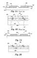
- FIGS. 1A and 1Bare schematic diagrams of prior art devices having a series interconnect architecture.
- FIG. 2Ais a schematic diagram of one embodiment of an optoelectronic device according to the present invention.
- FIG. 2Bshows a cross-sectional view of the device of FIG. 2A showing details relevant to fabrication.
- FIGS. 3A-3Care schematic diagrams illustrating one embodiment of a process according to the present invention for fabricating an optoelectronic device.
- FIG. 4is a schematic diagram of a hermetically packaged embodiment of an optoelectronic device according to the present invention.
- FIG. 5is a schematic diagram of an embodiment of an optoelectronic device according to the present invention having ribbon pixels.
- FIG. 2Ais a simplified schematic depiction of an optoelectronic device according to the present invention.
- Optoelectronic device 200includes continuous anode layer 212 , cathode areas 214 and 224 , and electroactive areas 216 and 226 sandwiched between continuous anode layer 212 and cathode areas 214 and 224 .
- Discontinuity 209is an opening in cathode 214 that may be a continuous line, a line segment, a circular opening, or any other shape.
- a plurality of connections to continuous anode 212are made at a first potential at 201 , 209 and 211 and at least one connection to cathode areas 214 and 224 at a second potential at connection point 213 .
- the size of the pixelmay be larger and the dark areas may be smaller compared to that of device 100 in FIGS. 1A and 1B , while maintaining the same brightness uniformity.
- FIG. 2Bshows a cross-sectional view of device 200 , showing details of its structure that are relevant to fabrication.
- the devicemay be constructed using the same process steps used to produce the series interconnection depicted in FIG. 2 except that continuous anode 212 is deposited as a continuous layer and no scribing is required.
- electroactive areas 216 and 226are formed by depositing continuous layers and then selectively removing (by solvent wiping or other process) to form scribe 202 .
- the electroactive layers that make up electroactive areas 216 and 226typically include multiple sublayers.
- sublayers that may be presentinclude hole injecting, hole transporting, light-emitting, electron transporting and electron injecting, and each of these sublayers may be composed of further sublayers.
- Cathode areas 214 and 224are formed by depositing a metal layer through a mask to form scribe 203 , co-located with scribe 202 .
- Electrode layer 202Electrical connection is made to anode layer 202 at voltage V 1 and to the cathode at voltage V 0 .
- the applied voltageis V and the current is now 2i.
- Additional electrical connectionsare primarily important for anode layer 202 , and secondarily important for cathode layer 204 , depending the sheet resistivity of each layer. Scribed region 202 / 203 may be either a hole (via) or a line.
- the cathode layer composed of cathode areas 214 and 224is an electrically continuous layer at one applied voltage, and cathode areas 214 and 224 are connected at a sufficient number of locations so that all portions of the cathode layer are electrically interconnected.
- cathode areas 214 and 224are electrically continuous and only one connection is required.
- scribe 203is a continuous line that separates a left and right portion of the cathode layer into cathode areas 214 and 224 , two connections are required to connect to both portions. Electrical connections to an external power source may be made at the edge and at the back of device 200 . In order to provide a device structure with the connections at the edge only, an additional conductive layer may be added.
- a process for fabricating an optoelectronic device according to the present inventionis shown schematically for device 300 in FIGS. 3A-3C .
- Continuous anode layer 312composed of ITO, is provided, optionally disposed on substrate 330 .
- the substrate 330may comprise glass, metal foil, or a plastic material, such as a polyester.
- the substratemay include a barrier layer (not shown), located between the glass, metal foil, or plastic material and anode layer 312 .
- Electroactive areas 316 and 326are disposed on continuous anode 312 , by depositing continuous layers and then selectively removing (by solvent wiping or other process) to form scribe 302 .
- electroactive areas 316 and 326may be deposited through a mask or die to form scribe 302 .
- Cathode areas 314 and 324are deposited on electroactive areas 316 and 326 through a mask to form scribe 303 .
- Suitable metalsinclude, but are not limited to, low work function materials such as aluminum, silver, calcium, magnesium, or a magnesium/silver alloy.
- the cathodemay be made of two layers to enhance electron injection.
- suitable materials for cathode areas 214 and 224are LiF/aluminum, Ca/aluminum, and Ca/silver.
- Insulating layer 342is then disposed on cathode areas 314 and 324 ; insulating layer 342 may be any thin film-forming organic or inorganic material, including, but not limited to, thermoplastic or thermosetting polymeric materials, such as epoxy, acrylic urethane, silicone, rubber, vinyl, or polyolefin.
- a suitable material for insulating layer 342is UV curable epoxy adhesive ELC2500, available from Electro-lite Corporation. Anode areas exposed by scribe 302 & 303 are masked using a masking tape.
- Cathode areas 314 and 324are coated with the adhesive using a wire rod, by spin coating, or using another known coating technique to achieve a thickness of 2 to 20 ⁇ m, and preferably about 5 to 10 ⁇ m.
- the adhesiveis exposed to UV radiation at a wavelength of 365 nm and an energy of 50 mW/cm 2 for 30 seconds.
- the masking tapeis removed to expose the anode in the selected locations.
- insulating layer 342may be deposited through a mask or patterned after depositing in a scribing operation to selectively to form areas depicted, as scribe 315 where anode 302 is exposed. In a subsequent step, shown in FIG.
- FIG. 3Bdepicts how multiple parallel connections may be made using the same method in a sectional view. Multiple connections are made to the anode to mitigate resistive losses as current moves laterally in the anode.
- the present inventionrelates to an optoelectronic device comprising a continuous unpatterned anode layer and a discontinuous cathode layer configured in a plurality of ribbon-like structures.
- ribbon-likerefers to the dimensions of lighted areas of the device, which may be long and narrow and thin in cross-section.
- the ribbonsmay be continuous with features and registration required in only the length dimension. That is, there is no registration or alignment requirement orthogonal to the length dimension of the ribbons. This feature simplifies the implementation of the ribbon design in a continuous roll to roll fabrication process.
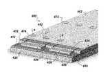
- FIG. 4illustrates hermetically packaged device 400 , composed of substrate 430 , continuous, unpatterned anode 412 , electroactive layers 426 , cathode areas 414 and 424 , (optional) anode bus 452 , 454 and 456 , feedthrough layer or backsheet 462 , anode conductive patches 472 and cathode conductive patches 482 .
- the conductive patches 472 and 482are composed of a conductive material, preferably a metal, and cover feedthrough apertures (not shown) that are configured to allow electrical connection between the anode and cathode areas and an external power source, and be electrically insulated form backsheet 462 .
- This configuration using an aperture and a patch to connect to a device and to form a hermetic package patchesis described in U.S.
- FIG. 5shows a top view of lighted hermetically packaged OLED device 500 , which includes ribbon-like lighted areas 514 , corresponding to luminescent areas under cathode, unlighted areas 552 , corresponding to areas covered by the anode bus, anode feedthrough apertures 582 and cathode feedthrough apertures 592 .
- FIGS. 4 and 5show external connection using conductive patches, connections may be made at the lateral areas of the device, as for the series interconnect architecture.
- OLED package 500is fabricated by a roll-to-roll process.
- a substrate with an optional barrier layer and a continuous unpatterned transparent conductive anode such as ITOis provided.
- An electroactive layerincluding, but not limited to, a light emitting layer, an optional hole injecting layer, an optional hole transporting layer, an optional electron transporting layer and an optional electron injecting layer is disposed on the anode and patterned by selectively removing portions of the material in the web direction.
- a cathode layeris deposited solely on the remaining portions of the electroactive layer, and an (optional) anode bus layer deposited simultaneously with the cathode layer solely on exposed areas of the anode to augment the conductivity of the ITO layer.
- Both the electroactive layer and the cathode layerare deposited in a continuous process without the need to stop the web to form a cross-web pattern. This is generally advantageous due to process and equipment simplification.
- An impermeable backsheetis laminated to the structure, the backsheet being provided with apertures that correspond to the locations of the anode and cathode connections.
- the aperturesare covered with impermeable patches that are in electrical contact with the anode or cathode, contact being provided by the use of a conductive adhesive, composed of, for example an acrylate or epoxy filled with conductive particle, or other means, and the patch is sealed to the backsheet.
- an external busis provided to connect the patches to a power supply and energize the device.
Landscapes
- Physics & Mathematics (AREA)
- Optics & Photonics (AREA)
- Electroluminescent Light Sources (AREA)
- Photovoltaic Devices (AREA)
Abstract
Description
Claims (10)
Priority Applications (7)
| Application Number | Priority Date | Filing Date | Title |
|---|---|---|---|
| US12/570,024US8137148B2 (en) | 2009-09-30 | 2009-09-30 | Method of manufacturing monolithic parallel interconnect structure |
| PCT/US2010/046812WO2011041050A1 (en) | 2009-09-30 | 2010-08-26 | Monolithic parallel interconnect structure |
| KR1020127010614AKR101801411B1 (en) | 2009-09-30 | 2010-08-26 | Monolithic parallel interconnect structure |
| EP10752951.3AEP2483944B1 (en) | 2009-09-30 | 2010-08-26 | Process for fabricating a monolithic parallel interconnect structure of an optoelectronic device |
| CN201080044936.4ACN102549797B (en) | 2009-09-30 | 2010-08-26 | Monolithic parallel interconnect structure |
| JP2012532089AJP5834009B2 (en) | 2009-09-30 | 2010-08-26 | Monolithic parallel interconnect structure |
| TW099132861ATWI602333B (en) | 2009-09-30 | 2010-09-28 | Photoelectric device and method of manufacturing the same |
Applications Claiming Priority (1)
| Application Number | Priority Date | Filing Date | Title |
|---|---|---|---|
| US12/570,024US8137148B2 (en) | 2009-09-30 | 2009-09-30 | Method of manufacturing monolithic parallel interconnect structure |
Publications (2)
| Publication Number | Publication Date |
|---|---|
| US20110074281A1 US20110074281A1 (en) | 2011-03-31 |
| US8137148B2true US8137148B2 (en) | 2012-03-20 |
Family
ID=43063997
Family Applications (1)
| Application Number | Title | Priority Date | Filing Date |
|---|---|---|---|
| US12/570,024Active2030-01-13US8137148B2 (en) | 2009-09-30 | 2009-09-30 | Method of manufacturing monolithic parallel interconnect structure |
Country Status (7)
| Country | Link |
|---|---|
| US (1) | US8137148B2 (en) |
| EP (1) | EP2483944B1 (en) |
| JP (1) | JP5834009B2 (en) |
| KR (1) | KR101801411B1 (en) |
| CN (1) | CN102549797B (en) |
| TW (1) | TWI602333B (en) |
| WO (1) | WO2011041050A1 (en) |
Cited By (2)
| Publication number | Priority date | Publication date | Assignee | Title |
|---|---|---|---|---|
| US20110012094A1 (en)* | 2009-07-15 | 2011-01-20 | Hyung Sup Lee | Electro-Optic Device and Method for Manufacturing the same |
| US9843019B2 (en) | 2014-01-24 | 2017-12-12 | Pioneer Oled Lighting Devices Corporation | Light emitting apparatus |
Families Citing this family (22)
| Publication number | Priority date | Publication date | Assignee | Title |
|---|---|---|---|---|
| US9675443B2 (en) | 2009-09-10 | 2017-06-13 | Johnson & Johnson Vision Care, Inc. | Energized ophthalmic lens including stacked integrated components |
| US8950862B2 (en) | 2011-02-28 | 2015-02-10 | Johnson & Johnson Vision Care, Inc. | Methods and apparatus for an ophthalmic lens with functional insert layers |
| US9110310B2 (en)* | 2011-03-18 | 2015-08-18 | Johnson & Johnson Vision Care, Inc. | Multiple energization elements in stacked integrated component devices |
| US10451897B2 (en) | 2011-03-18 | 2019-10-22 | Johnson & Johnson Vision Care, Inc. | Components with multiple energization elements for biomedical devices |
| US9233513B2 (en) | 2011-03-18 | 2016-01-12 | Johnson & Johnson Vision Care, Inc. | Apparatus for manufacturing stacked integrated component media inserts for ophthalmic devices |
| US9698129B2 (en)* | 2011-03-18 | 2017-07-04 | Johnson & Johnson Vision Care, Inc. | Stacked integrated component devices with energization |
| US9804418B2 (en) | 2011-03-21 | 2017-10-31 | Johnson & Johnson Vision Care, Inc. | Methods and apparatus for functional insert with power layer |
| US8674377B2 (en)* | 2011-08-30 | 2014-03-18 | General Electric Company | Optoelectronic device package, array and method of fabrication |
| KR20140117618A (en)* | 2012-01-26 | 2014-10-07 | 존슨 앤드 존슨 비젼 케어, 인코포레이티드 | Stacked integrated component media insert for an ophthalmic device |
| US8857983B2 (en) | 2012-01-26 | 2014-10-14 | Johnson & Johnson Vision Care, Inc. | Ophthalmic lens assembly having an integrated antenna structure |
| US10627651B2 (en) | 2014-08-21 | 2020-04-21 | Johnson & Johnson Vision Care, Inc. | Methods and apparatus to form biocompatible energization primary elements for biomedical devices with electroless sealing layers |
| US10361404B2 (en) | 2014-08-21 | 2019-07-23 | Johnson & Johnson Vision Care, Inc. | Anodes for use in biocompatible energization elements |
| US9793536B2 (en) | 2014-08-21 | 2017-10-17 | Johnson & Johnson Vision Care, Inc. | Pellet form cathode for use in a biocompatible battery |
| US9715130B2 (en) | 2014-08-21 | 2017-07-25 | Johnson & Johnson Vision Care, Inc. | Methods and apparatus to form separators for biocompatible energization elements for biomedical devices |
| US10361405B2 (en) | 2014-08-21 | 2019-07-23 | Johnson & Johnson Vision Care, Inc. | Biomedical energization elements with polymer electrolytes |
| US9383593B2 (en) | 2014-08-21 | 2016-07-05 | Johnson & Johnson Vision Care, Inc. | Methods to form biocompatible energization elements for biomedical devices comprising laminates and placed separators |
| US9599842B2 (en) | 2014-08-21 | 2017-03-21 | Johnson & Johnson Vision Care, Inc. | Device and methods for sealing and encapsulation for biocompatible energization elements |
| US10381687B2 (en) | 2014-08-21 | 2019-08-13 | Johnson & Johnson Vision Care, Inc. | Methods of forming biocompatible rechargable energization elements for biomedical devices |
| US9941547B2 (en) | 2014-08-21 | 2018-04-10 | Johnson & Johnson Vision Care, Inc. | Biomedical energization elements with polymer electrolytes and cavity structures |
| US10345620B2 (en) | 2016-02-18 | 2019-07-09 | Johnson & Johnson Vision Care, Inc. | Methods and apparatus to form biocompatible energization elements incorporating fuel cells for biomedical devices |
| JP2017182892A (en) | 2016-03-28 | 2017-10-05 | セイコーエプソン株式会社 | LIGHT EMITTING ELEMENT, LIGHT EMITTING DEVICE, AND ELECTRONIC DEVICE |
| CN107680497B (en)* | 2017-11-03 | 2019-12-03 | 京东方科技集团股份有限公司 | Manufacturing method of display substrate, display substrate, display panel and display device |
Citations (33)
| Publication number | Priority date | Publication date | Assignee | Title |
|---|---|---|---|---|
| JPS61138286A (en) | 1984-12-11 | 1986-06-25 | セイコーエプソン株式会社 | Liquid crystal electrooptic apparatus |
| US20040021425A1 (en) | 2002-08-05 | 2004-02-05 | Foust Donald Franklin | Series connected OLED structure and fabrication method |
| US20040140758A1 (en) | 2003-01-17 | 2004-07-22 | Eastman Kodak Company | Organic light emitting device (OLED) display with improved light emission using a metallic anode |
| JP2004251981A (en) | 2003-02-18 | 2004-09-09 | Seiko Epson Corp | Composite display |
| US6803720B2 (en) | 2000-12-15 | 2004-10-12 | Universal Display Corporation | Highly stable and efficient OLEDs with a phosphorescent-doped mixed layer architecture |
| JP2005017738A (en) | 2003-06-26 | 2005-01-20 | Seiko Epson Corp | Image display device |
| US6858878B2 (en)* | 2000-05-06 | 2005-02-22 | Semiconductor Energy Laboratory Co., Ltd. | Light-emitting device and electric apparatus |
| US20050052130A1 (en) | 2003-09-09 | 2005-03-10 | Toppoly Optoelectronics Corp. | Light emitting device with optical enhancement structure |
| US6870196B2 (en) | 2003-03-19 | 2005-03-22 | Eastman Kodak Company | Series/parallel OLED light source |
| US6885147B2 (en) | 1998-05-18 | 2005-04-26 | Emagin Corporation | Organic light emitting diode devices with improved anode stability |
| US20050093001A1 (en) | 2003-10-30 | 2005-05-05 | General Electric Company | Organic electro-optic device and method for making the same |
| US20050258436A1 (en) | 2004-05-21 | 2005-11-24 | Semiconductor Energy Laboratory Co., Ltd. | Lighting device |
| US20050270464A1 (en)* | 2004-06-03 | 2005-12-08 | Satoshi Seo | Lighting system |
| EP1612658A2 (en) | 2004-06-23 | 2006-01-04 | Sony Corporation | Display apparatus, display method, computer program and computer readable storage medium |
| US20060019573A1 (en)* | 2002-09-19 | 2006-01-26 | Samsung Sdi Co., Ltd. | Organic electroluminescent display and method of manufacturing the same |
| WO2006010911A2 (en) | 2004-07-27 | 2006-02-02 | Cambridge Display Technology Limited | Laminated interconnects for organic opto-electronic device modules |
| WO2006013373A2 (en) | 2004-08-04 | 2006-02-09 | Cambridge Display Technology Limited | Organic electroluminescent device |
| US20060049754A1 (en) | 2004-09-08 | 2006-03-09 | The Hong Kong University Of Science And Technology | Anode for organic light emitting diode |
| US20060066223A1 (en) | 2004-09-27 | 2006-03-30 | Florian Pschenitzka | Integrated fuses for OLED lighting device |
| US7034470B2 (en) | 2002-08-07 | 2006-04-25 | Eastman Kodak Company | Serially connecting OLED devices for area illumination |
| US7049741B2 (en) | 2004-01-27 | 2006-05-23 | Eastman Kodak Company | Organic light emitting diode with improved light emission through substrate |
| WO2006071106A1 (en) | 2004-12-27 | 2006-07-06 | Otb Group B.V. | Method for manufacturing an oled or a blank for forming an oled as well as such a blank or oled |
| WO2006078898A2 (en) | 2005-01-18 | 2006-07-27 | Nuelight Corporation | Top emission flat panel display with sensor feedback stabilization |
| US20060226522A1 (en) | 2005-03-29 | 2006-10-12 | Jie Liu | Full fault tolerant architecture for organic electronic devices |
| US7157156B2 (en) | 2004-03-19 | 2007-01-02 | Eastman Kodak Company | Organic light emitting device having improved stability |
| US20070001583A1 (en) | 2005-06-17 | 2007-01-04 | Fuji Photo Film Co., Ltd. | Light source, exposure apparatus, image display unit and medical device |
| US20070164667A1 (en)* | 2006-01-16 | 2007-07-19 | Samsung Electronics Co., Ltd | Display device and manufacturing method of the same |
| US20070200489A1 (en) | 2006-02-01 | 2007-08-30 | Poon Hak F | Large area organic electronic devices and methods of fabricating the same |
| US7307278B2 (en) | 2004-12-22 | 2007-12-11 | General Electric Company | Organic electronic devices having two dimensional series interconnections |
| US20080143250A1 (en) | 2006-12-14 | 2008-06-19 | Novaled Ag | Organisches Leuchtbauelement |
| US20080150418A1 (en)* | 2006-12-20 | 2008-06-26 | Lg.Philips Lcd Co., Ltd. | Organic electroluminescent device and method for manufacturing the same |
| US20080238310A1 (en) | 2007-03-30 | 2008-10-02 | Forrest Stephen R | OLED with improved light outcoupling |
| US20090023232A1 (en) | 2003-06-25 | 2009-01-22 | Yoshio Taniguchi | Organic electroluminescence element, process for preparation of the same, and electrode film |
Family Cites Families (12)
| Publication number | Priority date | Publication date | Assignee | Title |
|---|---|---|---|---|
| US6140766A (en)* | 1997-12-27 | 2000-10-31 | Hokuriku Electric Industry Co., Ltd. | Organic EL device |
| JPH11195492A (en)* | 1997-12-27 | 1999-07-21 | Hokuriku Electric Ind Co Ltd | Organic el element and its manufacture |
| JP2000133465A (en)* | 1998-10-30 | 2000-05-12 | Minnesota Mining & Mfg Co <3M> | Electroluminescent element and its manufacture |
| JP2001244069A (en)* | 2000-02-25 | 2001-09-07 | Seiko Epson Corp | Organic electroluminescence device |
| JP4423767B2 (en)* | 2000-08-22 | 2010-03-03 | ソニー株式会社 | Organic electroluminescent device and manufacturing method thereof |
| JP2002373779A (en)* | 2001-06-13 | 2002-12-26 | Sony Corp | Electric connection device and electronic equipment having electric connection device |
| JP2003045674A (en)* | 2001-08-02 | 2003-02-14 | Seiko Instruments Inc | Organic electroluminescent element |
| JP2003059653A (en)* | 2001-08-09 | 2003-02-28 | Sony Corp | Display device manufacturing method |
| JP2003086362A (en)* | 2001-09-12 | 2003-03-20 | Sony Corp | Display device, method of manufacturing the same, and electronic device |
| US20050129977A1 (en)* | 2003-12-12 | 2005-06-16 | General Electric Company | Method and apparatus for forming patterned coated films |
| JP2007027698A (en)* | 2005-06-17 | 2007-02-01 | Fujifilm Holdings Corp | Light source, exposure device, image display device and medical device |
| CN101589485B (en)* | 2007-01-22 | 2013-01-02 | 皇家飞利浦电子股份有限公司 | Light emitting device |
- 2009
- 2009-09-30USUS12/570,024patent/US8137148B2/enactiveActive
- 2010
- 2010-08-26KRKR1020127010614Apatent/KR101801411B1/enactiveActive
- 2010-08-26CNCN201080044936.4Apatent/CN102549797B/enactiveActive
- 2010-08-26WOPCT/US2010/046812patent/WO2011041050A1/enactiveApplication Filing
- 2010-08-26EPEP10752951.3Apatent/EP2483944B1/enactiveActive
- 2010-08-26JPJP2012532089Apatent/JP5834009B2/enactiveActive
- 2010-09-28TWTW099132861Apatent/TWI602333B/enactive
Patent Citations (35)
| Publication number | Priority date | Publication date | Assignee | Title |
|---|---|---|---|---|
| JPS61138286A (en) | 1984-12-11 | 1986-06-25 | セイコーエプソン株式会社 | Liquid crystal electrooptic apparatus |
| US6885147B2 (en) | 1998-05-18 | 2005-04-26 | Emagin Corporation | Organic light emitting diode devices with improved anode stability |
| US6858878B2 (en)* | 2000-05-06 | 2005-02-22 | Semiconductor Energy Laboratory Co., Ltd. | Light-emitting device and electric apparatus |
| US6803720B2 (en) | 2000-12-15 | 2004-10-12 | Universal Display Corporation | Highly stable and efficient OLEDs with a phosphorescent-doped mixed layer architecture |
| US7049757B2 (en) | 2002-08-05 | 2006-05-23 | General Electric Company | Series connected OLED structure and fabrication method |
| US20040021425A1 (en) | 2002-08-05 | 2004-02-05 | Foust Donald Franklin | Series connected OLED structure and fabrication method |
| US7034470B2 (en) | 2002-08-07 | 2006-04-25 | Eastman Kodak Company | Serially connecting OLED devices for area illumination |
| US20060019573A1 (en)* | 2002-09-19 | 2006-01-26 | Samsung Sdi Co., Ltd. | Organic electroluminescent display and method of manufacturing the same |
| US20040140758A1 (en) | 2003-01-17 | 2004-07-22 | Eastman Kodak Company | Organic light emitting device (OLED) display with improved light emission using a metallic anode |
| JP2004251981A (en) | 2003-02-18 | 2004-09-09 | Seiko Epson Corp | Composite display |
| US6870196B2 (en) | 2003-03-19 | 2005-03-22 | Eastman Kodak Company | Series/parallel OLED light source |
| US20090023232A1 (en) | 2003-06-25 | 2009-01-22 | Yoshio Taniguchi | Organic electroluminescence element, process for preparation of the same, and electrode film |
| JP2005017738A (en) | 2003-06-26 | 2005-01-20 | Seiko Epson Corp | Image display device |
| US20050052130A1 (en) | 2003-09-09 | 2005-03-10 | Toppoly Optoelectronics Corp. | Light emitting device with optical enhancement structure |
| US20050093001A1 (en) | 2003-10-30 | 2005-05-05 | General Electric Company | Organic electro-optic device and method for making the same |
| US7049741B2 (en) | 2004-01-27 | 2006-05-23 | Eastman Kodak Company | Organic light emitting diode with improved light emission through substrate |
| US7157156B2 (en) | 2004-03-19 | 2007-01-02 | Eastman Kodak Company | Organic light emitting device having improved stability |
| US20050258436A1 (en) | 2004-05-21 | 2005-11-24 | Semiconductor Energy Laboratory Co., Ltd. | Lighting device |
| US20050270464A1 (en)* | 2004-06-03 | 2005-12-08 | Satoshi Seo | Lighting system |
| EP1612658A2 (en) | 2004-06-23 | 2006-01-04 | Sony Corporation | Display apparatus, display method, computer program and computer readable storage medium |
| WO2006010911A2 (en) | 2004-07-27 | 2006-02-02 | Cambridge Display Technology Limited | Laminated interconnects for organic opto-electronic device modules |
| WO2006013373A2 (en) | 2004-08-04 | 2006-02-09 | Cambridge Display Technology Limited | Organic electroluminescent device |
| US20060049754A1 (en) | 2004-09-08 | 2006-03-09 | The Hong Kong University Of Science And Technology | Anode for organic light emitting diode |
| US20060066223A1 (en) | 2004-09-27 | 2006-03-30 | Florian Pschenitzka | Integrated fuses for OLED lighting device |
| US7307278B2 (en) | 2004-12-22 | 2007-12-11 | General Electric Company | Organic electronic devices having two dimensional series interconnections |
| WO2006071106A1 (en) | 2004-12-27 | 2006-07-06 | Otb Group B.V. | Method for manufacturing an oled or a blank for forming an oled as well as such a blank or oled |
| WO2006078898A2 (en) | 2005-01-18 | 2006-07-27 | Nuelight Corporation | Top emission flat panel display with sensor feedback stabilization |
| US20060226522A1 (en) | 2005-03-29 | 2006-10-12 | Jie Liu | Full fault tolerant architecture for organic electronic devices |
| US7518148B2 (en) | 2005-03-29 | 2009-04-14 | General Electric Company | Full fault tolerant architecture for organic electronic devices |
| US20070001583A1 (en) | 2005-06-17 | 2007-01-04 | Fuji Photo Film Co., Ltd. | Light source, exposure apparatus, image display unit and medical device |
| US20070164667A1 (en)* | 2006-01-16 | 2007-07-19 | Samsung Electronics Co., Ltd | Display device and manufacturing method of the same |
| US20070200489A1 (en) | 2006-02-01 | 2007-08-30 | Poon Hak F | Large area organic electronic devices and methods of fabricating the same |
| US20080143250A1 (en) | 2006-12-14 | 2008-06-19 | Novaled Ag | Organisches Leuchtbauelement |
| US20080150418A1 (en)* | 2006-12-20 | 2008-06-26 | Lg.Philips Lcd Co., Ltd. | Organic electroluminescent device and method for manufacturing the same |
| US20080238310A1 (en) | 2007-03-30 | 2008-10-02 | Forrest Stephen R | OLED with improved light outcoupling |
Non-Patent Citations (6)
| Title |
|---|
| JP2004251981 Abstract, Sep. 9, 2004. |
| JP2005017738 Abstract, Jan. 20, 2005. |
| JP61138286 Abstract, Jun. 25, 1986. |
| Machine translation, Koshihara JP 2004-251981 A.* |
| PCT International Search Report dated Nov. 19, 2010 and Written Opinion. |
| Search Report and Written Opinion from corresponding PCT Application No. PCT/US2011/021125 mailed on Jun. 8, 2011. |
Cited By (4)
| Publication number | Priority date | Publication date | Assignee | Title |
|---|---|---|---|---|
| US20110012094A1 (en)* | 2009-07-15 | 2011-01-20 | Hyung Sup Lee | Electro-Optic Device and Method for Manufacturing the same |
| US8399276B2 (en)* | 2009-07-15 | 2013-03-19 | Jusung Engineering Co., Ltd. | Electro-optic device and method for manufacturing the same |
| US9000454B2 (en) | 2009-07-15 | 2015-04-07 | Jusung Engineering Co., Ltd. | Electro-optic device and method for manufacturing the same |
| US9843019B2 (en) | 2014-01-24 | 2017-12-12 | Pioneer Oled Lighting Devices Corporation | Light emitting apparatus |
Also Published As
| Publication number | Publication date |
|---|---|
| US20110074281A1 (en) | 2011-03-31 |
| WO2011041050A1 (en) | 2011-04-07 |
| EP2483944B1 (en) | 2017-03-29 |
| TWI602333B (en) | 2017-10-11 |
| TW201131849A (en) | 2011-09-16 |
| JP5834009B2 (en) | 2015-12-16 |
| EP2483944A1 (en) | 2012-08-08 |
| CN102549797A (en) | 2012-07-04 |
| KR20120091123A (en) | 2012-08-17 |
| JP2013506958A (en) | 2013-02-28 |
| KR101801411B1 (en) | 2017-12-20 |
| CN102549797B (en) | 2015-03-25 |
Similar Documents
| Publication | Publication Date | Title |
|---|---|---|
| US8137148B2 (en) | Method of manufacturing monolithic parallel interconnect structure | |
| US8759884B2 (en) | Electronic device and method of manufacturing the same | |
| KR101468909B1 (en) | Organic functional device and manufacturing method therefor | |
| US8674377B2 (en) | Optoelectronic device package, array and method of fabrication | |
| KR101315086B1 (en) | Organic electronic device and method for manufacture thereof | |
| US8344389B2 (en) | Optoelectronic device array | |
| EP3429315B1 (en) | Lighting apparatus using organic light emitting diode and manufacturing method thereof | |
| KR20150129565A (en) | Organic light emitting device and method for manufacturing the same | |
| US9698387B2 (en) | Method for producing an optoelectronic component and method for patterning an organic, optoelectronic component | |
| US10418571B2 (en) | Lighting apparatus using organic light emitting device and method of fabricating thereof | |
| JP5680106B2 (en) | Electro-optical device, electrode for electro-optical device, and method and apparatus for producing electrode and electro-optical device provided with the electrode |
Legal Events
| Date | Code | Title | Description |
|---|---|---|---|
| AS | Assignment | Owner name:GENERAL ELECTRIC COMPANY, NEW YORK Free format text:ASSIGNMENT OF ASSIGNORS INTEREST;ASSIGNORS:FARQUHAR, DONALD SETON;DUGGAL, ANIL RAJ;HERZOG, MICHAEL SCOTT;AND OTHERS;SIGNING DATES FROM 20090929 TO 20090930;REEL/FRAME:023303/0290 | |
| FEPP | Fee payment procedure | Free format text:PAYOR NUMBER ASSIGNED (ORIGINAL EVENT CODE: ASPN); ENTITY STATUS OF PATENT OWNER: LARGE ENTITY | |
| STCF | Information on status: patent grant | Free format text:PATENTED CASE | |
| FPAY | Fee payment | Year of fee payment:4 | |
| AS | Assignment | Owner name:BOE TECHNOLOGY GROUP CO., LTD., CHINA Free format text:ASSIGNMENT OF ASSIGNORS INTEREST;ASSIGNOR:GENERAL ELECTRIC COMPANY;REEL/FRAME:038439/0315 Effective date:20151222 | |
| AS | Assignment | Owner name:BOE TECHNOLOGY GROUP CO., LTD., CHINA Free format text:ASSIGNMENT OF ASSIGNORS INTEREST;ASSIGNOR:GENERAL ELECTRIC COMPANY;REEL/FRAME:038490/0022 Effective date:20151222 | |
| MAFP | Maintenance fee payment | Free format text:PAYMENT OF MAINTENANCE FEE, 8TH YEAR, LARGE ENTITY (ORIGINAL EVENT CODE: M1552); ENTITY STATUS OF PATENT OWNER: LARGE ENTITY Year of fee payment:8 | |
| MAFP | Maintenance fee payment | Free format text:PAYMENT OF MAINTENANCE FEE, 12TH YEAR, LARGE ENTITY (ORIGINAL EVENT CODE: M1553); ENTITY STATUS OF PATENT OWNER: LARGE ENTITY Year of fee payment:12 |