US8136481B2 - Device for plasma treatment at atmospheric pressure - Google Patents
Device for plasma treatment at atmospheric pressureDownload PDFInfo
- Publication number
- US8136481B2 US8136481B2US12/207,585US20758508AUS8136481B2US 8136481 B2US8136481 B2US 8136481B2US 20758508 AUS20758508 AUS 20758508AUS 8136481 B2US8136481 B2US 8136481B2
- Authority
- US
- United States
- Prior art keywords
- electrode
- high voltage
- dielectric barrier
- voltage source
- voltage
- Prior art date
- Legal status (The legal status is an assumption and is not a legal conclusion. Google has not performed a legal analysis and makes no representation as to the accuracy of the status listed.)
- Expired - Fee Related, expires
Links
Images


Classifications
- H—ELECTRICITY
- H05—ELECTRIC TECHNIQUES NOT OTHERWISE PROVIDED FOR
- H05H—PLASMA TECHNIQUE; PRODUCTION OF ACCELERATED ELECTRICALLY-CHARGED PARTICLES OR OF NEUTRONS; PRODUCTION OR ACCELERATION OF NEUTRAL MOLECULAR OR ATOMIC BEAMS
- H05H1/00—Generating plasma; Handling plasma
- H05H1/24—Generating plasma
- H05H1/2406—Generating plasma using dielectric barrier discharges, i.e. with a dielectric interposed between the electrodes
Definitions
- the inventiongenerally relates to devices for plasma treatment at atmospheric pressure. More particular, the invention relates to devices for plasma treatment comprising an electrode, a dielectric barrier arranged directly in front of the electrode, and an AC high voltage source for applying an AC high voltage to the electrode to bring about a dielectric barrier gas discharge in a gas which is present in front of the dielectric barrier and which is at atmospheric pressure, in order to generate a plasma.
- German patent publication DE 199 57 775 C1discloses a device for plasma treatment of wood, wherein the wood is earthed to serve as a counter-electrode for the electrode having the dielectric barrier, to which the AC high voltage is applied.
- WO 2004/105810 A1From international patent application publication WO 2004/105810 A1 is it known to treat biologic materials containing living cells with a plasma.
- the gas dischargeis ignited between the electrode with the dielectric barrier and the biologic material by means of an AC high voltage applied to the electrode, wherein the biologic material serves as a capacitive counter-electrode for the electrode with the dielectric barrier.
- the electrode comprising the dielectric barrier which covers the electrodehas a tapering shape.
- the device known from WO 20041105810 A1is provided as a battery- or accumulator-powered, hand-held unit, its AC high voltage source being based on semiconductor technology.
- a plasma for a surface treatmentis generated by means of a dielectric barrier discharge at atmospheric pressure, this is up to now always done between an electrode with a dielectric barrier and some kind of a counter-electrode which is located at a certain distance to the electrode with the dielectric barrier, the gas in which the discharge is ignited being present between the electrode and the counter-electrode.
- WO 87/07248 A1discloses a device for treating objects using electric high voltage discharges in a gaseous media.
- a unipolar AC high voltageis applied to an electrode which comprises a number of needle-shaped extensions extending in parallel to each other and embedded into a dielectric. Open channels run through the dielectric in parallel to the needle-shaped extensions, through which a spark discharge, i.e. no dielectric barrier discharge, extends up to the main part of the electrode.
- the electrodeis arranged in front of the objects to be treated which are contacted electrically to provide a counter-electrode for the electrode.
- WO 02/065820 A1discloses a device for plasma treatment at atmospheric pressure, which has two opposing electrodes.
- One of the electrodesis earthed and provided with a dielectric barrier covering the electrode completely.
- a dielectric in front the other electrodewhich is connected to an AC high voltage source to apply an AC high voltage comprises open discharging gaps into which conductor electrodes extend from the other electrodes.
- the conductor electrodesare provides with pointed tips pointing towards the earthed electrode. Due to the concentration of the field strength of the electric field between the two electrodes at the pointed tips of the conductor electrodes, a gas discharge is ignited in a gas present between the two electrodes.
- This gas dischargeis only dielectrically barred by the dielectric in front of the earthed electrode, as the dielectric in front of the electrode connected to the AC high voltage source comprises the open discharge gaps.
- the known devicein constructed to introduce only gas in the space between the two electrodes. The plasma generated in the space between the electrodes may be used to treat surfaces located outside this space.
- German patent application publication DE 197 17 698 A1discloses a device for cleaning or activating electric circuit paths and surfaces of printed circuit boards.
- This devicecomprises a pair of opposing electrodes, at least one of which is provided with a dielectric barrier covering it completely.
- Emission tipswhich enhance the ignition of a gas discharge between the electrodes and homogenize the gas discharge are formed at the outer surface of one of the electrodes or of its dielectric barrier.
- the objects to be treatedare introduced between the electrodes of the known device and may rest on one of the electrodes or its dielectric barrier.
- Preferably only the opposing electrodehas emission tips.
- the emission tipsmay for example be made by etching the respective surface of a dielectric material. This results in radiuses of curvature of the tips of about 1 ⁇ m.
- the radiuses of curvature of the emission tipsare between 10 nm and 0.5 mm.
- the needle- or pin-shaped emission tipsmay be provided in a surface density of between 1 and 100 per cm 2 .
- the devices described up to hereare only poorly or even not at all suited for treating materials which are poor or even no electric conductors, like for example plastics, glasses and stones or even dry wood, as these materials may not effectively serve as counter-electrodes for the electrode with the dielectric barrier.
- Devices for generating potential-free plasmas in the form of a plasma beamwhich are sometimes designated as plasma-jets or plasma-blasters, are commercially offered. Such devices base on a different principle than a dielectric barrier discharge. As rule, they need a power grid connection or, at least, a gas connection. Further, these devices are very expensive.
- the present inventionrelates to a device for plasma treatment at atmospheric pressure, the device having an electrode; a dielectric barrier directly arranged in front of the electrode and covering a surface of the electrode; and an AC high voltage source for applying an AC high voltage to the electrode to bring about a dielectric barrier discharge in a gas at atmospheric pressure present in front of an outer surface of the dielectric barrier, in order to generate a plasma; wherein the device has no counter-electrode for the electrode with the dielectric barrier; wherein the electrode, at the surface of the electrode covered by the dielectric barrier, comprises a two-dimensional distribution of pointed tips pointing towards the gas present in front of the dielectric barrier; and wherein the outer surface of the dielectric barrier in front of which the gas is present is smooth.
- the present inventionrelates to a device for plasma treatment at atmospheric pressure, the device having an electrode; a dielectric barrier directly arranged in front of the electrode and covering a surface of the electrode; and a accumulator powered AC high voltage source for applying an AC high voltage to the electrode to bring about a dielectric barrier discharge in a gas at atmospheric pressure present in front of an outer surface of the dielectric barrier, in order to generate a plasma; wherein the AC high voltage source is designed so as to provide the AC high voltage as voltage pulse pairs of voltage pulses of alternating polarity at a repetition frequency of the voltage pulse pairs of less than 10,000 Hz and at a voltage amplitude of 5,000 volt to 60,000 volt; wherein the device has no counter-electrode for the electrode with the dielectric barrier; wherein the electrode, at the surface of the electrode covered by the dielectric barrier, comprises a two-dimensional distribution of pointed tips pointing towards the gas present in front of the dielectric barrier; wherein the outer surface of the dielectric barrier in front of which the gas is present
- a dielectric barrier dischargecan be brought about without any counter-electrode.
- the AC high voltage applied by the AC high voltage source to the electrode of the new device for plasma treatment at atmospheric pressureis able to ignite the plasma above any object to be treated independently of the electric properties of this object.
- the new deviceit is even possible to ignite a plasma in a volume which is only delimited by gas in front of the dielectric barrier, i.e. without any counter-electrode behind the gas.
- a dielectric barrier dischargeis also brought about in a surrounding of gas only with the new device, the gas itself providing the necessary electrical capacitance.
- the electrode of the new deviceis a two-dimensional electrode, the AC high voltage applied to the electrode by the AC high voltage source sustaining the plasma over the surface of the two-dimensional electrode extending in to linearly independent directions.
- the relevant surface of the two-dimensional electrode over which the gas discharge is brought aboutmay be at least 2 cm 2 .
- itis at least 4 cm 2 , more preferably at least 8 cm 2 . Nevertheless, the energy consumption of the device is kept within acceptable limits due to the dielectric barrier to the gas discharge.
- the electrode of the new deviceis a two-dimensional electrode is in no contradiction to the fact that it comprises pointed tips, which are pointing towards the gas in front of the dielectric barrier. Instead, these pointed tips, i.e. small areas of the two-dimensional electrode having a small radius of curvature, are used to sustain the plasma even without a counter-electrode.
- the pointed tips of the two-dimensional electrodehave a radius of curvature of less than 100 ⁇ m, more preferably of less than 10.0 ⁇ m.
- the height of the pointed tipsmay, at the same time, be comparatively small and may be less than 2 mm, preferably less than 1 mm or even less than 0.5 mm.
- the pointed tipsmay be provided as a sharply roughed-up surface of the electrode.
- the pointed tipsare provided in a two-dimensional distribution, i.e. not only as a single row of needles arranged side by side.
- the surface density of the pointed tipsmay have an order of magnitude of 1 to 100,000 pointed tips per cm 2 .
- the electrodeof an electrically conductive powder which is arranged in a ceramic solid body providing the dielectric barrier.
- the powder as suchprovides a high number of suitable pointed tips.
- a further important measure to enable the new device to ignite or sustain a plasma without any counter-electrodeis that the AC high voltage applied by the AC high voltage source to the electrode comprises a steep voltage increase or rise of at least 5,000 volt/ ⁇ s, preferably of at least 10,000 volt/ ⁇ s. Particularly good results are obtained with a voltage rise of about 12,000 volt/ ⁇ s.
- the AC high voltage applied by the AC high voltage source to the electrodecomprises voltage pulses display a voltage rise period of up to 5 ⁇ s, preferably of less than 3 ⁇ s, a pulse duration of less than 10 ⁇ s, preferably of less than 6 ⁇ s, and an amplitude of 5,000 volt to 60,000 volt, preferably of 5,000 volt to about 40,000 volt.
- These voltage pulsesmay have alternating polarity, i.e. be bipolar. Bipolar pulses are an advantage, however, they are not absolutely necessary.
- a repetition frequency of the voltage pulses of the AC high voltage sourcemay be smaller than 10,000 Hz. Preferably it is even smaller than 5,000 Hz; and particularly it may be in the range of 500 to 2,000 Hz. I.e. the repetition frequency of the voltage pulses is much smaller than the reciprocal value of the duration of the voltage pulses.
- the voltage pulsesare comprised of bipolar pulse pairs or groups of voltage pulse pairs which are separated by pauses.
- An AC high voltage source which is able to generate the AC high voltage described heremay be manufactured in semiconductor technology using standard parts in compact dimensions. Thus, it is possible, to make the whole new device as a hand-held unit, which may even be battery- or accumulator-operated. Particularly, the new device may have the size of a commercially available cordless screwdriver. Thus, a very compact and portable hand-held unit is provided.
- a controller for the AC high voltageis preferred which avoids an un-controlled increase of the output power of the device so that the device may for example not be misused as a so-called “taser”.
- a controllermay for example determine a feedback of a load capacitance to the input side of an ignition transformer of the AC high voltage source which is connected to the electrode at its output side, and use this information as an input value for controlling the output power of the AC high voltage source.
- the controller of the AC high voltage sourceis able to keep the output power of the AC high voltage source constant by varying the output voltage of the AC high voltage source and/or the pulse repetition rate of the voltage pulses of the AC high voltage.
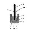
- FIG. 1shows the construction of a first embodiment of the new device for plasma treatment at atmospheric pressure, its electrode being depicted in a cross sectional view.
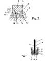
- FIG. 2shows the application of a plasma ignited by means of the device according to FIG. 1 to a poorly electrically conducting surface.
- FIG. 3shows a cross section through the front area of an electrode of a second embodiment of the device.
- FIG. 4sketches the construction of the new device as an accumulator-operated hand-held unit.
- FIG. 5shows the voltage curve of an AC high voltage applied to the electrode of the new device, which consists of bipolar voltage pulse pairs;
- FIG. 6shows the general construction of a controller for the AC high voltage applied to the electrode of the hand-held unit according to FIG. 4 .
- FIG. 1shows a device 1 for plasma treatment at atmospheric pressure of surfaces which are not depicted here.
- device 1has an electrode 2 which is provided with a dielectric barrier 3 made of a suitable closed dielectric material, like for example a dense ceramic.
- a high voltage lead 4 having an electric isolation 5 connecting to dielectric barrier 3leads to electrode 2 .
- An AC high voltageis supplied to electrode 2 by an AC high voltage source 6 via high voltage lead 4 .
- AC high voltage source 6is based on semiconductor parts, and it is supplied with electric energy by an energy supply 7 which may be one or several batteries or accumulators or a mains adaptor. AC high voltage which will be more detailed explained with regard to FIG.
- gas discharge 9is a dielectric barrier discharge so that the energy output of the device 1 by means of the gas discharge is suitably limited.
- Gas discharge 9results in a plasma 11 of reactive components, like for example radicals of gas 10 , by means of which a surface can be activated for a successive coating to increase its adhesive properties, for example.
- the plasma 11may be generated with the device 1 independently of the electric conductivity of a surface to be treated and may be used for treating the surface.
- FIG. 2illustrates the treatment of a surface 12 of a body 13 with the plasma 11 . Due to the presence of the surface 12 in the surroundings of the electrode 2 the gas discharge and thus the plasma 11 are concentrated to the space between the electrode 2 and the surface 12 , despite an only small electric conductivity of the material of the body 13 .
- FIG. 3illustrates an actual embodiment of the electrode 2 and its surface 14 provided with microscopic pointed tips.
- the material of the electrode 2is sinter bronze in powder form which is also designated as bronze powder.
- the sinter bronzeis simply poured into the dielectric barrier 3 made as a ceramic solid body 23 , and a metal pin 24 forming the high voltage lead 4 is pressed into its center. At its back end, the area of the sinter bronze 21 is closed by an electrically isolating sealing mass 22 . It is important in the new device to generate high field strengths in order to ignite a gas discharge over the dielectric barrier 3 .
- the sinter bronzeprovides sufficient suitable pointed tips to this end.
- the electric conductivity of a powder forming the electrode 2 with the pointed tips at the surface 14does not need to be particularly high.
- the new device 1may be provided as a portable hand-held unit 16 , like it is depicted in FIG. 4 .
- the energy supply 7is an accumulator block
- the AC high voltage source 6is provided within a casing 17 having a trigger-shaped operation switch 18 .
- the operation switch 18Upon pressing the operation switch 18 the AC high voltage is applied to the electrode 2 , and, independently of whether a counter-electrode is present or not, a plasma is ignited in front of the outer surface 15 of the dielectric barrier 3 of the electrode 2 and sustained as long as the operation switch 18 is pressed.
- the AC high voltagemay be made of voltage pulses 19 and 20 depicted in FIG. 5 , each positive voltage pulse 19 , which increases within few microseconds up to a voltage of 40,000 to 50,000 volt being directly followed by a negative voltage pulse 20 , which approximately has the same course of the voltage over the time as the voltage pulse 19 but an opposite polarity. Then, a pause follows before a next pair of voltage pulses 19 and 20 is applied to the electrode 2 .
- the fast voltage increaseallows for igniting the gas discharge 9 independently of any counter-electrode, and the following very fast change of the polarity of the voltage allows for a successive back-ignition of the gas discharge, in which the previously separated charges of the gas serve as a kind of substitute for a counter-electrode.
- the intervals of the bipolar voltage pulse pairs 19 , 20may have an order of magnitude of 1 millisecond, without all free electrons of the plasma recombining in the meanwhile, so that the plasma may be built up again by the following voltage pulse pair starting from the remaining ionization.
- FIG. 6shows the basic design of a preferred controller for the AC high voltage applied to the electrode of the hand-held unit 16 according to FIG. 4 .
- An output load of an ignition transformer 25which has an effect on the input side of an ignition transformer 25 is registered, i.e. measured, at the input side. This information is used as an input value for the controller for the output AC high voltage.
- the counter-induction of the secondary winding of the ignition transformer 25is directed against the self-induction of its primary winding.
- the effect of the counter-induction of the secondary winding on the primary windingincreases with the load on the secondary circuit.
- the amount of the voltage over the primary winding of the ignition transformer 25thus decreases with increasing load at the output side or secondary winding.
- the voltage over the primary windingthus behaves exactly opposite to the load at the output side. This effect is used for controlling the ignition voltage.
- the voltage amplitudeis adjusted by means of a potentiometer.
- the potentiometeris replaced by a transistor, i.e. a current-controlled resistor, within the circuitry 26 of the AC high voltage source.
- the rectified and filtered self-induction voltage over the primary windingis applied via an appropriately tuned amplifier circuit having a rectifier 27 , a filter 28 and a controller 29 . This provides for a control loop. Strictly speaking, the output voltage is kept constant instead of the output power in this basic design.
- the pulse repetition rate of the voltage pulses 19 and 20 or the output voltagehas to be adjusted to a varying load capacitance.
- Variable load capacitancesoccur due to different objects in front of the surface 15 of the dielectric barrier 3 .
- P1 ⁇ 2 ⁇ C ⁇ U 2 ⁇ f I.e. small changes in the output voltage have a strong effect on the output power.
- the output voltagemay be varied over a large area depending on the ratio of this increase of the pulse repetition rate and of the change of the output voltage.
- a particular embodiment of the new device 1 constructed as a hand-held unit 16may have the following technical data:
- the output voltageis controlled depending on the load at the output within a range of 5 to 35 kvolt (5 to 35 thousand volt).
- the loaddepends on an object arranged in front of the surface 15 of the dielectric barrier.
- the pulse repetition ratechanges in the opposite direction to the height of the pulse amplitude within a range of 500 to 2,000 Hz. With a maximum output amplitude of 35 kvolt, the pulse repetition rate has a maximum value of about 500 Hz. The maximum value of the pulse repetition rate of ca, 2,000 Hz is achieved with the minimum output amplitude of about 5 kvolt.
- the ignition voltageis automatically adjusted to the material, i.e. the electrical capacitance and conductivity of the object to be treated.
- the ignition voltagemay be surveyed by means of a LED at the backside of the casing 17 , for example. When the LED glows, the output voltage is between 20 and 35 kvolt, this corresponds roughly to the voltage necessary for treating wooden surfaces. If the LED does not glow or another LED glows, the output voltage is about 5 to 20 kvolt which corresponds to the necessary voltage for treating metal surfaces.
Landscapes
- Physics & Mathematics (AREA)
- Engineering & Computer Science (AREA)
- Plasma & Fusion (AREA)
- Spectroscopy & Molecular Physics (AREA)
- Plasma Technology (AREA)
Abstract
Description
P=½·C·U2·f
I.e. small changes in the output voltage have a strong effect on the output power. By means of a simultaneous adjustment of the pulse repetition rate, however, the influence of an output voltage change may be attenuated. The output voltage may be varied over a large area depending on the ratio of this increase of the pulse repetition rate and of the change of the output voltage.
- 1 device
- 2 electrode
- 3 dielectric barrier
- 4 high voltage lead
- 5 isolation
- 6 AC high voltage source
- 7 energy supply
- 8 edge
- 9 gas discharge
- 10 gas
- 11 plasma
- 12 surface
- 13 body
- 14 surface
- 15 surface
- 16 hand-held unit
- 17 casing
- 18 switch
- 19 voltage pulse
- 20 voltage pulse
- 21 sinter bronze
- 22 sealing mass
- 23 ceramic solid body
- 24 metal pin
- 25 ignition transformer
- 26 AC circuitry
- 27 rectifier
- 28 filter
- 29 controller
Claims (16)
Applications Claiming Priority (4)
| Application Number | Priority Date | Filing Date | Title |
|---|---|---|---|
| DE102006011312.8 | 2006-03-11 | ||
| DE102006011312ADE102006011312B4 (en) | 2006-03-11 | 2006-03-11 | Apparatus for plasma treatment under atmospheric pressure |
| DE102006011312 | 2006-03-11 | ||
| PCT/EP2007/002143WO2007104512A1 (en) | 2006-03-11 | 2007-03-12 | Device for plasma treatment at atmospheric pressure |
Related Parent Applications (1)
| Application Number | Title | Priority Date | Filing Date |
|---|---|---|---|
| PCT/EP2007/002143ContinuationWO2007104512A1 (en) | 2006-03-11 | 2007-03-12 | Device for plasma treatment at atmospheric pressure |
Publications (2)
| Publication Number | Publication Date |
|---|---|
| US20090009090A1 US20090009090A1 (en) | 2009-01-08 |
| US8136481B2true US8136481B2 (en) | 2012-03-20 |
Family
ID=38222666
Family Applications (1)
| Application Number | Title | Priority Date | Filing Date |
|---|---|---|---|
| US12/207,585Expired - Fee RelatedUS8136481B2 (en) | 2006-03-11 | 2008-09-10 | Device for plasma treatment at atmospheric pressure |
Country Status (4)
| Country | Link |
|---|---|
| US (1) | US8136481B2 (en) |
| EP (1) | EP1997358B1 (en) |
| DE (1) | DE102006011312B4 (en) |
| WO (1) | WO2007104512A1 (en) |
Cited By (2)
| Publication number | Priority date | Publication date | Assignee | Title |
|---|---|---|---|---|
| US20120259270A1 (en)* | 2009-12-24 | 2012-10-11 | Dirk Wandke | Electrode arrangement for a dielectric barrier discharge plasma treatment and method for plasma treatment of a surface |
| US20150343231A1 (en)* | 2014-05-30 | 2015-12-03 | Cold Plasma Medical Technologies, Inc. | Wearable Cold Plasma System |
Families Citing this family (20)
| Publication number | Priority date | Publication date | Assignee | Title |
|---|---|---|---|---|
| EP2324687B1 (en) | 2008-08-20 | 2016-01-27 | Vision Dynamics Holding B.V. | Device for generating a plasma discharge for patterning the surface of a substrate |
| EP2180768A1 (en)* | 2008-10-23 | 2010-04-28 | TNO Nederlandse Organisatie voor Toegepast Wetenschappelijk Onderzoek | Apparatus and method for treating an object |
| DE102009020163B4 (en)* | 2009-05-07 | 2012-07-19 | Fraunhofer-Gesellschaft zur Förderung der angewandten Forschung e.V. | Method for interlayer-free bonding of substrates, apparatus for carrying out a plasma treatment and their use |
| GB0920124D0 (en) | 2009-11-17 | 2009-12-30 | Linde Ag | Device for generating gaseous species |
| US9078540B2 (en)* | 2010-08-24 | 2015-07-14 | Steve Hoffman | Process and device for forming a low adhesion cooking surface |
| DE102011000261A1 (en)* | 2011-01-21 | 2012-07-26 | Hochschule für angewandte Wissenschaft und Kunst Fachhochschule Hildesheim/Holzminden/Göttingen | Dielectric coplanar discharge source for surface treatment under atmospheric pressure |
| CN102573259A (en)* | 2012-01-13 | 2012-07-11 | 北京交通大学 | Method for suppressing filamentary discharge and electrode structure |
| DE102012103470A1 (en) | 2012-04-20 | 2013-10-24 | Hochschule für Angewandte Wissenschaft und Kunst - Hildesheim/Holzminden/Göttingen | plasma Roller |
| DE102012015482A1 (en)* | 2012-08-07 | 2014-02-13 | Cinogy Gmbh | Electrode arrangement for a disabled plasma |
| DE102013100617B4 (en)* | 2013-01-22 | 2016-08-25 | Epcos Ag | Device for generating a plasma and handheld device with the device |
| DE102013107448B4 (en)* | 2013-07-15 | 2016-11-24 | Relyon Plasma Gmbh | Arrangement for germ reduction by means of plasma |
| JP5924462B1 (en) | 2014-10-23 | 2016-05-25 | 住友電気工業株式会社 | Method for manufacturing silicon carbide substrate |
| CA3090944A1 (en)* | 2017-02-08 | 2018-08-16 | Upstream Data Inc. | Blockchain mine at oil or gas facility |
| CN107911931A (en)* | 2017-12-01 | 2018-04-13 | 南京苏曼等离子科技有限公司 | Atmospheric pressure low temperature plasma treatment seed equipment and operation method |
| CN112703824A (en)* | 2018-09-26 | 2021-04-23 | 莱雅公司 | Device for generating cold plasma comprising an electrode and a dielectric |
| CN111298295B (en)* | 2020-04-01 | 2021-11-16 | 珠海格力电器股份有限公司 | Air plasma generating device and medical equipment with same |
| DE102021124377A1 (en) | 2021-09-21 | 2023-03-23 | Cinogy Gmbh | Electrode arrangement for a plasma discharge |
| US12162217B2 (en)* | 2021-09-29 | 2024-12-10 | NEXA3D Inc. | Three-dimensional printer head including a dielectric barrier discharge (DBD) disk and a transformer assembly |
| DE102021128964B3 (en) | 2021-11-08 | 2023-03-09 | Hochschule für angewandte Wissenschaft und Kunst Hildesheim/Holzminden/Göttingen, Körperschaft des öffentlichen Rechts | Process and device for generating plasmas with increased pulse energy by means of dielectrically impeded electrical discharges |
| DE102023108314A1 (en)* | 2023-03-31 | 2024-10-02 | Friederike Kogelheide | plasma applicator with a high-voltage generator |
Citations (12)
| Publication number | Priority date | Publication date | Assignee | Title |
|---|---|---|---|---|
| WO1987007248A1 (en) | 1986-05-31 | 1987-12-03 | Oliver Sieke | Process and device for treating objects |
| US5603893A (en) | 1995-08-08 | 1997-02-18 | University Of Southern California | Pollution treatment cells energized by short pulses |
| DE19717698A1 (en) | 1997-04-26 | 1998-10-29 | Fraunhofer Ges Forschung | Method and device for cleaning activation of electrical conductor tracks and circuit board surfaces |
| DE19957775C1 (en) | 1999-12-01 | 2000-07-13 | Wolfgang Vioel | Modification of wood surfaces uses an electrode fed with alternating high voltages which generates an electrical discharge under atmospheric pressure to cover the wood surface |
| WO2000079843A1 (en) | 1999-06-23 | 2000-12-28 | Skion Corporation | Apparatus for plasma treatment using capillary electrode discharge plasma shower |
| EP1073091A2 (en) | 1999-07-27 | 2001-01-31 | Matsushita Electric Works, Ltd. | Electrode for plasma generation, plasma treatment apparatus using the electrode, and plasma treatment with the apparatus |
| US20010020582A1 (en) | 1999-04-28 | 2001-09-13 | Hana Barankova | Method and apparatus for plasma treatment of gas |
| WO2002065820A1 (en) | 2001-02-12 | 2002-08-22 | Se Plasma Inc. | Apparatus for generating low temperature plasma at atmospheric pressure |
| JP2003133291A (en) | 2001-10-26 | 2003-05-09 | Sekisui Chem Co Ltd | Discharge plasma treatment apparatus and discharge plasma treatment method using it |
| WO2004051729A2 (en) | 2002-12-04 | 2004-06-17 | Süss Mircro Tec Lithography Gmbh | Method and device for pre-treating surfaces of substrates to be bonded |
| WO2004105810A1 (en) | 2003-06-03 | 2004-12-09 | Fachhochschule Hildesheim/Holzminden/ Göttingen | Treatment of biological material containing living cells using a plasma generated by a gas discharge |
| US20060239873A1 (en)* | 2004-08-23 | 2006-10-26 | Echnologoes Ltd. | Double dielectric barrier discharge electrode device and system |
- 2006
- 2006-03-11DEDE102006011312Apatent/DE102006011312B4/ennot_activeExpired - Fee Related
- 2007
- 2007-03-12EPEP07723189.2Apatent/EP1997358B1/ennot_activeNot-in-force
- 2007-03-12WOPCT/EP2007/002143patent/WO2007104512A1/enactiveApplication Filing
- 2008
- 2008-09-10USUS12/207,585patent/US8136481B2/ennot_activeExpired - Fee Related
Patent Citations (17)
| Publication number | Priority date | Publication date | Assignee | Title |
|---|---|---|---|---|
| WO1987007248A1 (en) | 1986-05-31 | 1987-12-03 | Oliver Sieke | Process and device for treating objects |
| US5603893A (en) | 1995-08-08 | 1997-02-18 | University Of Southern California | Pollution treatment cells energized by short pulses |
| DE19717698A1 (en) | 1997-04-26 | 1998-10-29 | Fraunhofer Ges Forschung | Method and device for cleaning activation of electrical conductor tracks and circuit board surfaces |
| US20010020582A1 (en) | 1999-04-28 | 2001-09-13 | Hana Barankova | Method and apparatus for plasma treatment of gas |
| WO2000079843A1 (en) | 1999-06-23 | 2000-12-28 | Skion Corporation | Apparatus for plasma treatment using capillary electrode discharge plasma shower |
| US20020092616A1 (en) | 1999-06-23 | 2002-07-18 | Seong I. Kim | Apparatus for plasma treatment using capillary electrode discharge plasma shower |
| US6489585B1 (en) | 1999-07-27 | 2002-12-03 | Matsushita Electric Works, Ltd. | Electrode for plasma generation, plasma treatment apparatus using the electrode, and plasma treatment with the apparatus |
| EP1073091A2 (en) | 1999-07-27 | 2001-01-31 | Matsushita Electric Works, Ltd. | Electrode for plasma generation, plasma treatment apparatus using the electrode, and plasma treatment with the apparatus |
| DE19957775C1 (en) | 1999-12-01 | 2000-07-13 | Wolfgang Vioel | Modification of wood surfaces uses an electrode fed with alternating high voltages which generates an electrical discharge under atmospheric pressure to cover the wood surface |
| WO2002065820A1 (en) | 2001-02-12 | 2002-08-22 | Se Plasma Inc. | Apparatus for generating low temperature plasma at atmospheric pressure |
| JP2003133291A (en) | 2001-10-26 | 2003-05-09 | Sekisui Chem Co Ltd | Discharge plasma treatment apparatus and discharge plasma treatment method using it |
| WO2004051729A2 (en) | 2002-12-04 | 2004-06-17 | Süss Mircro Tec Lithography Gmbh | Method and device for pre-treating surfaces of substrates to be bonded |
| US20060234472A1 (en) | 2002-12-04 | 2006-10-19 | Markus Gabriel | Method and device for pre-treating surfaces of substrates to be bonded |
| WO2004105810A1 (en) | 2003-06-03 | 2004-12-09 | Fachhochschule Hildesheim/Holzminden/ Göttingen | Treatment of biological material containing living cells using a plasma generated by a gas discharge |
| DE10324926B3 (en) | 2003-06-03 | 2005-02-03 | Fachhochschule Hildesheim/Holzminden/Göttingen | Apparatus for treating a biological cell containing living cells with a plasma generated by a gas discharge |
| US20060084158A1 (en) | 2003-06-03 | 2006-04-20 | Wolfgang Viol | Treatment of biological material containing living cells using a plasma generated by a gas discharge |
| US20060239873A1 (en)* | 2004-08-23 | 2006-10-26 | Echnologoes Ltd. | Double dielectric barrier discharge electrode device and system |
Non-Patent Citations (1)
| Title |
|---|
| English Translation of PCT Search Report mailed Nov. 3, 2008 in co-pending related application No. PCT/EP20071002143. 6 Pages. |
Cited By (5)
| Publication number | Priority date | Publication date | Assignee | Title |
|---|---|---|---|---|
| US20120259270A1 (en)* | 2009-12-24 | 2012-10-11 | Dirk Wandke | Electrode arrangement for a dielectric barrier discharge plasma treatment and method for plasma treatment of a surface |
| US9005188B2 (en)* | 2009-12-24 | 2015-04-14 | Cinogy Gmbh | Electrode arrangement for a dielectric barrier discharge plasma treatment and method for plasma treatment of a surface |
| US20150343231A1 (en)* | 2014-05-30 | 2015-12-03 | Cold Plasma Medical Technologies, Inc. | Wearable Cold Plasma System |
| US9498637B2 (en)* | 2014-05-30 | 2016-11-22 | Plasmology4, Inc. | Wearable cold plasma system |
| US20170106200A1 (en)* | 2014-05-30 | 2017-04-20 | Plasmology4, Inc. | Wearable Cold Plasma System |
Also Published As
| Publication number | Publication date |
|---|---|
| DE102006011312A1 (en) | 2007-10-04 |
| US20090009090A1 (en) | 2009-01-08 |
| EP1997358A1 (en) | 2008-12-03 |
| WO2007104512A1 (en) | 2007-09-20 |
| DE102006011312B4 (en) | 2010-04-15 |
| EP1997358B1 (en) | 2014-01-01 |
Similar Documents
| Publication | Publication Date | Title |
|---|---|---|
| US8136481B2 (en) | Device for plasma treatment at atmospheric pressure | |
| EP2756516B1 (en) | Cold plasma treatment devices and associated methods | |
| Valdivia-Barrientos et al. | Analysis and electrical modelling of a cylindrical DBD configuration at different operating frequencies | |
| US9664386B2 (en) | Dynamic flame control | |
| KR101577207B1 (en) | Portable plasma apparatus for improving skin | |
| JP5305828B2 (en) | Method and apparatus for sensory stimulation | |
| Xian et al. | Multiple plasma bullet behavior of an atmospheric-pressure plasma plume driven by a pulsed dc voltage | |
| KR101942362B1 (en) | Plasma beauty device | |
| US11792910B2 (en) | Process for producing ozone and apparatus for ozone generation | |
| CN109310461A (en) | Non-thermal plasma emitters and devices for control | |
| WO2021072371A3 (en) | Multi-electrode/multi-modal atmospheric pressure glow discharge plasma ionization device | |
| Monge-Dauge et al. | Experimental study coupled with electrical modeling for the consideration of DBD-based plasma jet | |
| Kuo et al. | Design and electrical characteristics of a modular plasma torch | |
| KR20190116900A (en) | Plasma beauty device | |
| Chiper et al. | On surface elementary processes and polymer surface modifications induced by double pulsed dielectric barrier discharge | |
| Hong et al. | Measurement of the surface charging of a plasma actuator using surface DBD | |
| Vongphouthone et al. | Model of the homogeneous electrical discharge | |
| Bozhko et al. | Corona discharge to water surface and its transition to a spark | |
| Tepper et al. | Effects of interface between dielectric barrier and electrode on homogeneous barrier discharges at atmospheric pressure | |
| US7251195B1 (en) | Apparatus for generating an acoustic signal | |
| Thapa et al. | Study of dielectric barrier discharge in air and estimation of electron density and energy deposition | |
| JP6725938B2 (en) | Ion generator | |
| Zhao et al. | Characterization of Battery‐Powered Portable Ar Plasma Jets Contacting Human Impedance Model and Its Safety Assessment for Direct Human Treatment | |
| RU2499321C1 (en) | Device to produce stable microdischarge of atmospheric pressure | |
| JP2017224589A (en) | Ion generator |
Legal Events
| Date | Code | Title | Description |
|---|---|---|---|
| AS | Assignment | Owner name:FACHHOCHSCHULE HILDESHEIM/HOLZMINDEN/GOTTINGEN, GE Free format text:ASSIGNMENT OF ASSIGNORS INTEREST;ASSIGNORS:VIOL, WOLFGANG, DR.;BORN, STEFAN;KAEMLING, ANDY;REEL/FRAME:021764/0522 Effective date:20080910 | |
| ZAAA | Notice of allowance and fees due | Free format text:ORIGINAL CODE: NOA | |
| ZAAB | Notice of allowance mailed | Free format text:ORIGINAL CODE: MN/=. | |
| STCF | Information on status: patent grant | Free format text:PATENTED CASE | |
| FEPP | Fee payment procedure | Free format text:PAYOR NUMBER ASSIGNED (ORIGINAL EVENT CODE: ASPN); ENTITY STATUS OF PATENT OWNER: SMALL ENTITY | |
| FPAY | Fee payment | Year of fee payment:4 | |
| MAFP | Maintenance fee payment | Free format text:PAYMENT OF MAINTENANCE FEE, 8TH YR, SMALL ENTITY (ORIGINAL EVENT CODE: M2552); ENTITY STATUS OF PATENT OWNER: SMALL ENTITY Year of fee payment:8 | |
| REFU | Refund | Free format text:REFUND - PAYMENT OF MAINTENANCE FEE, 8TH YR, SMALL ENTITY (ORIGINAL EVENT CODE: R2552); ENTITY STATUS OF PATENT OWNER: SMALL ENTITY | |
| FEPP | Fee payment procedure | Free format text:MAINTENANCE FEE REMINDER MAILED (ORIGINAL EVENT CODE: REM.); ENTITY STATUS OF PATENT OWNER: SMALL ENTITY | |
| LAPS | Lapse for failure to pay maintenance fees | Free format text:PATENT EXPIRED FOR FAILURE TO PAY MAINTENANCE FEES (ORIGINAL EVENT CODE: EXP.); ENTITY STATUS OF PATENT OWNER: SMALL ENTITY | |
| STCH | Information on status: patent discontinuation | Free format text:PATENT EXPIRED DUE TO NONPAYMENT OF MAINTENANCE FEES UNDER 37 CFR 1.362 | |
| FP | Lapsed due to failure to pay maintenance fee | Effective date:20240320 |