US8134424B2 - Electrostatic connector - Google Patents
Electrostatic connectorDownload PDFInfo
- Publication number
- US8134424B2 US8134424B2US12/257,612US25761208AUS8134424B2US 8134424 B2US8134424 B2US 8134424B2US 25761208 AUS25761208 AUS 25761208AUS 8134424 B2US8134424 B2US 8134424B2
- Authority
- US
- United States
- Prior art keywords
- conductor portion
- conductor
- electrode portion
- connector
- dielectric
- Prior art date
- Legal status (The legal status is an assumption and is not a legal conclusion. Google has not performed a legal analysis and makes no representation as to the accuracy of the status listed.)
- Expired - Fee Related, expires
Links
Images


Classifications
- H—ELECTRICITY
- H01—ELECTRIC ELEMENTS
- H01R—ELECTRICALLY-CONDUCTIVE CONNECTIONS; STRUCTURAL ASSOCIATIONS OF A PLURALITY OF MUTUALLY-INSULATED ELECTRICAL CONNECTING ELEMENTS; COUPLING DEVICES; CURRENT COLLECTORS
- H01R24/00—Two-part coupling devices, or either of their cooperating parts, characterised by their overall structure
- H01R24/38—Two-part coupling devices, or either of their cooperating parts, characterised by their overall structure having concentrically or coaxially arranged contacts
- H01R24/40—Two-part coupling devices, or either of their cooperating parts, characterised by their overall structure having concentrically or coaxially arranged contacts specially adapted for high frequency
- H01R24/42—Two-part coupling devices, or either of their cooperating parts, characterised by their overall structure having concentrically or coaxially arranged contacts specially adapted for high frequency comprising impedance matching means or electrical components, e.g. filters or switches
- H01R24/44—Two-part coupling devices, or either of their cooperating parts, characterised by their overall structure having concentrically or coaxially arranged contacts specially adapted for high frequency comprising impedance matching means or electrical components, e.g. filters or switches comprising impedance matching means
- H—ELECTRICITY
- H01—ELECTRIC ELEMENTS
- H01R—ELECTRICALLY-CONDUCTIVE CONNECTIONS; STRUCTURAL ASSOCIATIONS OF A PLURALITY OF MUTUALLY-INSULATED ELECTRICAL CONNECTING ELEMENTS; COUPLING DEVICES; CURRENT COLLECTORS
- H01R2103/00—Two poles
Definitions
- the present inventionrelates to a connector for performing transmission of signals using electrostatic coupling.
- An electrical connectoris used to perform transmission of signals in various electrical devices.
- electrical contacts facing each otherare brought into contact to perform transmission of signals. In this case, the electrical contacts deteriorate as a result of long term use.
- electrostatic coupling connectoror capacitance coupling connector as means for performing transmission of signals in a contactless manner (no contact) which does not require any contact point.
- an electrostatic coupling apparatuswhich can transmit signals even in the case of a structure in which one part rotates.
- the second prior exampleprovides a structure in which electrostatic capacitance is constituted by a first cylindrical electrode and a second cylindrical electrode arranged coaxially with the first cylindrical electrode in proximity thereto in an outer peripheral position and one of the first cylindrical electrode and the second cylindrical electrode is rotatable, enabling transmission of signals between the first cylindrical electrode and the second cylindrical electrode.
- the present inventionis a connector for transmitting signals with another electrode portion facing thereto insulated in terms of direct current using electrostatic coupling, comprises:
- an inner electrode portionhaving a facing area larger than a cross-sectional area of the inner first conductor portion in a direction perpendicular to a direction of the common axis, and facing the other electrode portion;
- a ratio of outer diameter of the inner second conductor portion to inner diameter of the outer second conductor portionis set to provide substantially fixed characteristic impedance at every position of the inner second conductor portion and the outer second conductor portion along the direction of the common axis.
- a connector of the present inventionhas a first connector and a second connector connected so as to face each other insulated in terms of direct current using electrostatic coupling,
- At least one of the first connector and the second connectorcomprises:
- an inner electrode portionhaving a facing area larger than a cross-sectional area of the inner first conductor portion in a direction perpendicular to a direction of the common axis, and facing an inner electrode portion of the opposite connector;
- a ratio of outer diameter of the inner second conductor portion to inner diameter of the outer second conductor portionis set to provide substantially fixed characteristic impedance at every position of the inner second conductor portion and the outer second conductor portion along the direction of the common axis.
- FIG. 1is a vertical sectional view showing the structure of an electrostatic coupling connector of an embodiment 1 of the present invention
- FIG. 2is a front view of the electrostatic coupling connector of an embodiment 1;
- FIG. 3is a vertical sectional view showing the structure of an electrostatic coupling connector of an embodiment 2 of the present invention
- FIG. 4is a side view showing the structure of an electrostatic coupling connector of a variation of the embodiment 2 with part thereof cut away;
- FIG. 5is a vertical sectional view showing the structure of an electrostatic coupling connector of an embodiment 3 of the present invention.
- FIG. 6is a vertical sectional view showing the structure of an electrostatic coupling connector of an embodiment 4 of the present invention.
- FIG. 7is a diagram showing the relative dielectric constant of a dielectric used in the embodiment 4 in the direction of transmission of signals;
- FIG. 8is a side view showing the structure of an electrostatic coupling connector of an embodiment 5 of the present invention with part thereof cut away;
- FIG. 9is a diagram showing the average relative dielectric constant of two dielectrics used in the embodiment 5 in the direction of transmission of signals.
- FIGS. 1 and 2relate to an embodiment 1 of the present invention.
- FIG. 1shows the structure of an electrostatic coupling connector which is the embodiment 1 of the connector of the present invention in a vertical sectional view.
- FIG. 2shows a front view seeing the structure of the electrostatic coupling connector from the electrode portion side.
- an electrostatic coupling connector 1 of the embodiment 1 of the present inventionhas a first conductor portion 3 formed on the proximal end side thereof connected to one end of a coaxial cable 2 . Signals transmitted from the other end of the coaxial cable 2 to the one end of the same are transmitted via a second conductor portion 4 electrically connected to the first conductor portion 3 to an electrode portion 5 provided on an end portion of the second conductor portion 4 .
- first conductor portion 3 , the second conductor portion 4 and the electrode portion 5are formed integrally using metal such as brass, for example.
- metalsuch as brass, for example.
- separate bodiesmay be electrically connected.
- silver, gold or the like, which have low electrical resistance and good electrical conductivity,may be formed on the surface of them by plating or the like.
- silver or the like of good electrical conductivitymay be formed on the surface portion of the conductor (electrode) between an inner first conductor portion 3 a and an outer first conductor portion 3 b constituting the first conductor portion 3 , between an inner second conductor portion 4 a and an outer second conductor portion 4 b constituting the second conductor portion 4 , and between an inner electrode portion 5 a and an outer electrode portion 5 b constituting the electrode portion 5 .
- the electrode portion 5When the electrostatic coupling connectors 1 and 6 are connected, the electrode portion 5 is in proximity to the electrode portion 7 of the electrostatic coupling connector 6 facing thereto. In this case, the electrode portion 5 and the electrode portion 7 face each other in proximity, spaced by the thickness of a thin insulating plate 8 interposed therebetween, for example.
- a protruding portion 10 protruding to the electrostatic coupling connector 1 sideis provided as a connector connecting portion, inside which the electrode portion 5 of the electrostatic coupling connector 1 is fitted thereby to set the both electrostatic coupling connectors 1 and 6 in the connection state.
- the protruding portion 10is formed of the same conductor as the outer electrode portion 7 b , where transmission of signals is performed by electrostatic coupling between the inner electrode portions 5 a and 7 a on the inner side.
- the portion shown by double-dotted dashed line of the protruding portion 10may be formed of an insulator, for example.
- a signal transmitted by the coaxial cable 2is transmitted via the electrostatic coupling connector 1 of the embodiment 1 from the electrode portion 5 thereof to the electrode portion 7 facing the electrode portion 5 by electrostatic coupling or electrostatic induction.
- the insulating plate 8has a structure which insulates the whole end faces of the both electrode portions 5 and 7 in the specific example shown in FIG. 1 , it may also have a structure which insulates only the portions of the inner electrode portion 5 a and the inner electrode portion 7 a facing thereto with the insulating plate 8 and brings the outer electrode portion 5 b and the outer electrode portion 7 b into electrical contact.
- the electrostatic coupling connector 1has a rotationally symmetrical shape which is rotationally symmetrical about a central axis O thereof.
- the first conductor portion 3 , the second conductor portion 4 and the electrode portion 5respectively comprise the inner first conductor portion 3 a and the outer first conductor portion 3 b , the inner second conductor portion 4 a and the outer second conductor portion 4 b , and the inner electrode portion 5 a and the outer electrode portion 5 b , having coaxial shapes (or coaxial structures) about the common central axis O. Signals are transmitted along the (axial) direction of this common axis.
- a dielectric 9 of fluorine-based resinfor example, being electrically insulative, having low dielectric loss and having a certain dielectric constant is filled between the inner first conductor portion 3 a and the outer first conductor portion 3 b , between the inner second conductor portion 4 a and the outer second conductor portion 4 b , and between the inner electrode portion 5 a and the outer electrode portion 5 b.
- the dielectric 9is also filled between the inner electrode portion 7 a and the outer electrode portion 7 b which constitute the electrode portion 7 of the same size as the electrode portion 5 , facing the electrode portion 5 .
- the inner second conductor portion 4 a and the outer second conductor portion 4 b of the second conductor portion 4have the same outer and inner diameters as the inner first conductor portion 3 a and the outer first conductor portion 3 b , respectively.
- the inner second conductor portion 4 ahas the same outer diameter d 1 a as the inner first conductor portion 3 a
- the outer second conductor portion 4 bhas the same inner diameter D 1 b as the outer first conductor portion 3 b (with regard to d 1 a , D 1 b , see FIG. 2 ).
- the second conductor portion 4has a tapered shape with its diameter linearly increased toward the electrode portion 5 side; at the connecting portion with the electrode portion 5 , the inner second conductor portion 4 a and the outer second conductor portion 4 b respectively have the same outer diameter d 2 a and inner diameter D 2 b as the inner electrode portion 5 a and the outer electrode portion 5 b (with regard to d 2 a , D 2 b , see FIG. 2 ).
- the values of the outer diameter d 2 x and the inner diameter D 2 xvary with the ratio of D 2 x /d 2 x being constant.
- An inner conductor 2 a and an outer conductor 2 b of the coaxial cable 2are respectively connected to the proximal ends of the inner first conductor portion 3 a and the outer first conductor portion 3 b .
- a dielectric 11is filled between the inner conductor 2 a and the outer conductor 2 b of the coaxial cable 2 .
- the coaxial cable 2is shown in FIG. 1 as an example of the signal transmitting member for transmitting signals to the inner first conductor portion 3 a and the outer first conductor portion 3 b , it is not limited thereto and may also be one of a coaxial tube structure the outer conductor of which is formed with a copper tube or the like, for example.
- signal transmissionis performed in the TEM mode (Transverse electromagnetic Mode) in the coaxial structure portion in which the dielectric is filled between the inner conductor and the outer conductor of the coaxial cable 2 , the electrostatic coupling connector 1 , the other electrostatic coupling connector 6 and the like.
- TEM modeTransverse electromagnetic Mode
- logrepresents the common logarithm having 10 as the base.
- the outer diameter of the inner first conductor portion 3 ais d 1 a
- the inner diameter of the outer first conductor portion 3 bis D 1 b
- the relative dielectric constant of the dielectric 9is E 1 as shown in FIG. 2
- the outer diameter d 1 a , the inner diameter D 1 b and the relative dielectric constant ⁇ 1are so set as to match the characteristic impedance Zo of the coaxial cable 2 when the formula (1) is applied.
- the dielectrics 9 and 11have the same relative dielectric constant ⁇ 1 , for example, they may be set at different values.
- Zocharacteristic impedance value
- the electrode portion 7 facing the electrode portion 5has the same size as the electrode portion 5 .
- the outer diameter of the inner electrode portion 7 a in the electrode portion 7is d 2 a and the inner diameter of the outer electrode portion 7 b is D 2 b.
- the characteristic impedance Zhas the predetermined characteristic impedance value Zo.
- the electrostatic coupling connector 1has a structure in which no impedance mismatch is generated in terms of the characteristic impedance.
- the electrostatic coupling connector 1has a structure which can prevent the occurrence of reflection to perform signal transmission.
- the difference between the values of surface conductor lengths La, Lb (the surface lengths of the tapered shapes) corresponding to (signal) transmission path lengths L′a, L′b for signal transmission of the outer surface of the inner second conductor portion 4 a and the inner surface of the outer second conductor portion 4 b in the second conductor portion 4is restricted to a predetermined value V (>0) or less.
- the formula (2)can also be represented, using the transmission path lengths L′a, L′b, as L′a ⁇ L′b ⁇ V′ (2′).
- V′( ⁇ 1) 1/2 *V.
- the common dielectric 9 having a certain dielectric constantis filled between the inner second conductor portion 4 a and the outer second conductor portion 4 b , and restriction is provided as in the formula (2) using the surface conductor length (restriction may also be provided as in the formula (2′) using the transmission path length).
- the difference in arrival timecan be suppressed in the case of transmitting signals from the connecting portion with the first conductor portion 3 to the connecting portion with the electrode portion 5 by means of the inner second conductor portion 4 a side and the outer second conductor portion 4 b.
- the value of the outer diameter of the inner second conductor portion 4 ais linearly increased in the present embodiment, it is non-linearly increased in a later-described embodiment.
- the electrode portion 7 facing the electrode portion 5is set to have the same size as the electrode portion 5 which has a large electrode area, so that reflection due to impedance mismatch upon transmission of signals can be suppressed as well as signals of low frequency range can be transmitted with little attenuation.
- the outer diameter of the inner electrode portion 7 ais d 2 a and the inner diameter of the outer electrode portion 7 b is D 2 b in the electrode portion 7 .
- the electrostatic coupling connector 6 of the example shown in FIG. 1is shown by means of an exemplary structure in which the diameters of the inner conductor portion and the outer conductor portion do not change in the direction of transmission of signals.
- the outer diameter of the inner conductor portionis equal to the outer diameter d 2 a of the inner electrode portion 7 a
- the inner diameter of the outer conductor portionis equal to the inner diameter D 2 b of the outer electrode portion 7 b.
- the other electrostatic coupling connector 6 to which the electrostatic coupling connector 1 of the present embodiment is attachable and detachableis not limited to the exemplary structure shown in FIG. 1 but may also have a structure which changes in a tapered shape in the direction of transmission of signals in the same way as the electrostatic coupling connector 1 , for example (see a tapered shape as in FIG. 3 as an example which relates to an embodiment 2 described later).
- the inner second conductor portion 4 ahas its cross-sectional area increased in diameter in a tapered shape (more strictly, such that the cross-sectional area monotonically increases) along the axial direction of the common axis from the connection portion with the inner first conductor portion 3 a up to the connecting portion with the inner electrode portion 5 , and the outer second conductor portion 4 b arranged outside thereof is set to have inner diameter which keeps a certain characteristic impedance with the outer diameter of the inner second conductor portion 4 a.
- a signal transmitted from the coaxial cable 2 side, for example, to the electrostatic coupling connector 1can be transmitted to the first conductor portion 3 , the second conductor portion 4 and the electrode portion 5 without the occurrence of reflection due to impedance mismatch or the like, and further the signal can be transmitted from the electrode portion 5 to the electrode portion 7 in proximity thereto having the same size of facing area by means of electrostatic coupling while suppressing the occurrence of reflection.
- the electrode portion 5is larger than the cross-sectional area of the first conductor portion 3 and is set to have the same size as the electrode portion 7 facing thereto, the occurrence of reflection due to impedance mismatch can be suppressed as well as attenuation upon transmission at the electrostatic coupling portion can be reduced (suppressed) in terms of signals or signal components in a low range (low frequency).
- the present embodimentcan be realized with a simple configuration.
- FIG. 3shows an electrostatic coupling connector 1 B of an embodiment 2 of the present invention.
- the electrostatic coupling connector 1 of the embodiment 1has a structure in which a dielectric 9 having one relative dielectric constant (value) is filled between the inner conductor portion and the outer conductor portion.
- dielectrics 9 a , 9 b of different relative dielectric constants ⁇ a, ⁇ bare filled at least between the inner second conductor portion 4 a and the outer second conductor portion 4 b in the second conductor portion 4 .
- the settingis such that the relative dielectric constant ⁇ b of the dielectric 9 b which is filled so as to contact with the inner surface of the outer second conductor portion 4 b is smaller than the relative dielectric constant ⁇ a of the dielectric 9 a which is filled so as to contact with the outer surface of the inner second conductor portion 4 a.
- the signal transmission rate in the surface conductor length Lb on the outer second conductor portion 4 b sidecan be higher than the signal transmission rate in the surface conductor length La on the inner second conductor portion 4 a side.
- the predetermined value V′ of the formula (2′)can be set to be a small value even when the gradient of the tapered shape (as the surface shape) of the second conductor portion 4 is large.
- the value V′ of the formula (2′)can, of course, be a small value, and can also be set to be 0. That is, the difference in arrival time of signals in the inner conductor and the outer conductor of the second conductor portion 4 can be further suppressed.
- reflection due to impedance mismatchcan be avoided with a simple structure in the same way as the embodiment 1 as well as the electrostatic coupling connector 1 B suitable for transmission of low frequency signals can be realized.
- the gradient of the tapered shape of the second conductor portion 4can be larger than in the embodiment 1.
- the length L of the second conductor portion 4can be short. Therefore, the electrostatic coupling connector 1 B of the present embodiment can reduce the size, weight and cost.
- the gradient of the tapered shapecan be large as described above, the area of the electrode portion 5 can be large even if the length L of the second conductor portion 4 is short.
- the other electrostatic coupling connector 6 B to which the electrostatic coupling connector 1 B is detachably connectedmay have a structure in which the size does not change in the direction of transmission of signals as shown in FIG. 1 , the case of a structure similar to the electrostatic coupling connector 1 B is shown in the example of FIG. 3 .
- the second conductor portion 4 ′ adjacent to the electrode portion 7has a structure similar to the second conductor portion 4 .
- dielectrics 9 a ′, 9 b ′ similar to the dielectrics 9 a , 9 b in the case of the electrode portion 5are filled between the inner electrode portion 7 a and the outer electrode portion 7 b in the electrode portion 7 .
- the electrostatic coupling connector 1 B shown in FIG. 3two dielectrics 9 a , 9 b are filled in the second conductor portion 4 and the electrode portion 5 , for example.
- the first conductor portion 3is shown by means of an exemplary structure in which only one dielectric 9 a , for example, is filled in the interior space.
- the characteristic impedance of the second conductor portion 4is set to be continuous at the connecting portion with the first conductor portion 3 and the connecting portion with the electrode portion 5 . Therefore, the structure can suppress the occurrence of reflection upon transmission of signals.
- FIG. 4shows an electrostatic coupling connector 1 C of a first variation in which a dielectric 9 c adopting air as the dielectric 9 b in FIG. 3 is provided.
- the same dielectric 9 as the embodiment 1is used as the dielectric 9 a.
- the dielectric 9 b portionmay simply be air in the same way as in FIG. 3 (however, since the value of dielectric constant differs from that of the dielectric 9 b , strictly the tapered shape differs).
- the structureis such that the dielectric 9 c of air is formed only in the second conductor portion 4 portion and the dielectric 9 is filled in the first conductor portion 3 and the electrode portion 5 on both ends thereof, thereby securing sufficient strength for supporting.
- the outer surface of the inner second conductor portion 4 a of the second conductor portion 4is in close contact with the dielectric 9 , and the inner peripheral surface of the outer second conductor portion 4 b contacts with the dielectric 9 c of air.
- FIG. 5shows an electrostatic coupling connector 1 D of an embodiment 3 of the present invention.
- the electrostatic coupling connector 1 D of the present embodimenthas a structure similar to the electrostatic coupling connector 1 of an embodiment 1 up to the midway portion of the second conductor portion 4 in the first conductor portion 3 side of the second conductor portion 4 .
- a dielectric 9 d having a dielectric constant smaller than the dielectric 9 used in the first conductor portion 3 sideis filled between the inner second conductor portion 4 a and the outer second conductor portion 4 b in the second conductor portion 4 , for example.
- the dielectric 9 dmay be air. In this case, there may be no filling between the inner second conductor portion 4 a and the outer second conductor portion 4 b.
- the shape of the outer surface of the inner second conductor portion 4 ais protruding outwardly in the radial direction so as to form a curved surface portion 13 smoothly bending in the direction of transmission of signals, as shown in FIG. 5 .
- the outer diameter of the inner second conductor portion 4 asmoothly protrudes as the curved surface portion 13 in order to restrain the amount of change of the characteristic impedance around that position.
- the signal transmission path at this portioncan be larger (than in the case of the above-described tapered shape, that is, a conical surface).
- the configurationis in other respects the same as an embodiment 1 or the like.
- FIG. 6shows an electrostatic coupling connector 1 E of an embodiment 4 of the present invention.
- a dielectric 9 e having a dielectric constant which substantially continuously varies to be smaller with advancing in the direction of transmission of signals in the second conductor portion 4is filled in place of the dielectric 9 having a certain dielectric constant in the electrostatic coupling connector 1 of the embodiment 1, for example.
- FIG. 7a characteristic example of the relative dielectric constant of the dielectric 9 e in the direction of transmission of signals is shown in FIG. 7 .
- the ratio of mixture of a dielectric 9 a of fluorine-based resin, for example, and a dielectric 9 b , for example, having a dielectric constant smaller than that of the formeris varied so that the relative dielectric constant in the direction of transmission of signals varies linearly and continuously.
- the variationis not limited to linear one as shown in FIG. 7 .
- airmay be used as the dielectric 9 b .
- the ratio at which minute volume of air is mixed in the dielectric 9 amay be varied continuously, for example, to form the dielectric 9 e of fluorine-based resin or the like in the form of a sponge.
- the outer diameter of the inner second conductor portion 4 acan be varied more greatly than in the case of filling with the dielectric 9 .
- the outer diameter of the inner second conductor portion 4 athat is, the gradient of the surface of the tapered shape can be large as compared to the inner diameter of the outer second conductor portion 4 b.
- the present embodimentalso has effects similar to the embodiment 2.
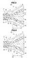
- FIG. 8shows an electrostatic coupling connector 1 F of an embodiment 5 of the present invention.
- the electrostatic coupling connector 1 F of the present embodimentis similar to the electrostatic coupling connector 1 E of the embodiment 4 and therefore can be regarded as a variation of the embodiment 4.
- the electrostatic coupling connector 1 F of the present embodimenthas a characteristic of the dielectric constant of the hollow portion between the inner second conductor portion 4 a and the outer second conductor portion 4 b in the second conductor portion 4 varying to be smaller substantially continuously with advancing toward the direction of transmission of signals, in the same way as the electrostatic coupling connector 1 E of the embodiment 4.
- FIG. 9shows the characteristic of the average relative dielectric constant at every position x in the direction of transmission of signals in the case of the present embodiment. This characteristic is the same as FIG. 7 . However, since the relative dielectric constant changes stepwise in the radial direction in the present embodiment, the value of FIG. 9 is the average of the two relative dielectric constants in the radial direction.
- the relative dielectric constant in the hollow portionis set to be a uniform value in the radial direction in the case of the embodiment 4, two dielectrics 9 a , 9 b are arranged such that the dielectric constant changes stepwise in the radial direction in the present embodiment.
- the settingis such that at least the side contacting with the inner second conductor portion 4 a has large dielectric constants and the side contacting with the outer second conductor portion 4 b has small dielectric constants.
- the present embodimenthas substantially the same effects as in the case of the embodiment 4.
- Embodiments configured such as by partially combining the above-described embodiments and the likeare also part of the present invention.
- the above-described embodiments and the likeare described by means of the case of electrostatic coupling connectors for performing signal transmission by means of electrostatic coupling, they can also applied to cases other than electrostatic coupling.
- the electrostatic coupling connector 1 of the embodiment 1when one desires to perform signal transmission by directly connecting two coaxial cables of different cross-sectional sizes, to the thinner coaxial cable side may the electrostatic coupling connector 1 of the embodiment 1, for example, and to the other coaxial cable may the electrostatic coupling connector 6 respectively be connected to perform transmission of signals by means of the electrostatic coupling connectors 1 , 6 .
- the insulating plate 8is removed. Also in such a case, signal transmission can be performed with reduced reflection as compared to the case of directly connecting two coaxial cables of different cross-sectional sizes.
Landscapes
- Coupling Device And Connection With Printed Circuit (AREA)
- Details Of Connecting Devices For Male And Female Coupling (AREA)
Abstract
Description
Z=(138/(εo)1/2)log(Do/do)[Ω] (1).
Here, log represents the common logarithm having 10 as the base.
(Lb−La)<V (2)
is set. Since Lb>La, the inequality is shown not using the absolute value. Here, the surface conductor lengths La, Lb and the transmission path lengths L′a, L′b have the relationship:
L′a=(ε1)1/2*La, L′b=(ε1)1/2*Lb (3),
for example.
L′a−L′b<V′ (2′).
Here, V′=(ε1)1/2*V.
εa>εb (4)
is set.
Claims (36)
Applications Claiming Priority (2)
| Application Number | Priority Date | Filing Date | Title |
|---|---|---|---|
| JP2007279218AJP5064969B2 (en) | 2007-10-26 | 2007-10-26 | connector |
| JP2007-279218 | 2007-10-26 |
Publications (2)
| Publication Number | Publication Date |
|---|---|
| US20090111315A1 US20090111315A1 (en) | 2009-04-30 |
| US8134424B2true US8134424B2 (en) | 2012-03-13 |
Family
ID=40583414
Family Applications (1)
| Application Number | Title | Priority Date | Filing Date |
|---|---|---|---|
| US12/257,612Expired - Fee RelatedUS8134424B2 (en) | 2007-10-26 | 2008-10-24 | Electrostatic connector |
Country Status (2)
| Country | Link |
|---|---|
| US (1) | US8134424B2 (en) |
| JP (1) | JP5064969B2 (en) |
Cited By (163)
| Publication number | Priority date | Publication date | Assignee | Title |
|---|---|---|---|---|
| US9042812B1 (en) | 2013-11-06 | 2015-05-26 | At&T Intellectual Property I, Lp | Surface-wave communications and methods thereof |
| US9113347B2 (en) | 2012-12-05 | 2015-08-18 | At&T Intellectual Property I, Lp | Backhaul link for distributed antenna system |
| US9209902B2 (en) | 2013-12-10 | 2015-12-08 | At&T Intellectual Property I, L.P. | Quasi-optical coupler |
| US20160049740A1 (en)* | 2014-08-12 | 2016-02-18 | Commscope Technologies Llc | Coaxial cable and connector with capacitive coupling |
| US9312919B1 (en) | 2014-10-21 | 2016-04-12 | At&T Intellectual Property I, Lp | Transmission device with impairment compensation and methods for use therewith |
| US9461706B1 (en) | 2015-07-31 | 2016-10-04 | At&T Intellectual Property I, Lp | Method and apparatus for exchanging communication signals |
| US9490869B1 (en) | 2015-05-14 | 2016-11-08 | At&T Intellectual Property I, L.P. | Transmission medium having multiple cores and methods for use therewith |
| US9503189B2 (en) | 2014-10-10 | 2016-11-22 | At&T Intellectual Property I, L.P. | Method and apparatus for arranging communication sessions in a communication system |
| US9509415B1 (en) | 2015-06-25 | 2016-11-29 | At&T Intellectual Property I, L.P. | Methods and apparatus for inducing a fundamental wave mode on a transmission medium |
| US9520945B2 (en) | 2014-10-21 | 2016-12-13 | At&T Intellectual Property I, L.P. | Apparatus for providing communication services and methods thereof |
| US9525210B2 (en) | 2014-10-21 | 2016-12-20 | At&T Intellectual Property I, L.P. | Guided-wave transmission device with non-fundamental mode propagation and methods for use therewith |
| US9525524B2 (en) | 2013-05-31 | 2016-12-20 | At&T Intellectual Property I, L.P. | Remote distributed antenna system |
| US9531427B2 (en) | 2014-11-20 | 2016-12-27 | At&T Intellectual Property I, L.P. | Transmission device with mode division multiplexing and methods for use therewith |
| US9564947B2 (en) | 2014-10-21 | 2017-02-07 | At&T Intellectual Property I, L.P. | Guided-wave transmission device with diversity and methods for use therewith |
| US9577306B2 (en) | 2014-10-21 | 2017-02-21 | At&T Intellectual Property I, L.P. | Guided-wave transmission device and methods for use therewith |
| US9608740B2 (en) | 2015-07-15 | 2017-03-28 | At&T Intellectual Property I, L.P. | Method and apparatus for launching a wave mode that mitigates interference |
| US9608692B2 (en) | 2015-06-11 | 2017-03-28 | At&T Intellectual Property I, L.P. | Repeater and methods for use therewith |
| US9615269B2 (en) | 2014-10-02 | 2017-04-04 | At&T Intellectual Property I, L.P. | Method and apparatus that provides fault tolerance in a communication network |
| US9628116B2 (en) | 2015-07-14 | 2017-04-18 | At&T Intellectual Property I, L.P. | Apparatus and methods for transmitting wireless signals |
| US9628854B2 (en) | 2014-09-29 | 2017-04-18 | At&T Intellectual Property I, L.P. | Method and apparatus for distributing content in a communication network |
| US9640850B2 (en) | 2015-06-25 | 2017-05-02 | At&T Intellectual Property I, L.P. | Methods and apparatus for inducing a non-fundamental wave mode on a transmission medium |
| US9653770B2 (en) | 2014-10-21 | 2017-05-16 | At&T Intellectual Property I, L.P. | Guided wave coupler, coupling module and methods for use therewith |
| US9654173B2 (en) | 2014-11-20 | 2017-05-16 | At&T Intellectual Property I, L.P. | Apparatus for powering a communication device and methods thereof |
| US9667317B2 (en) | 2015-06-15 | 2017-05-30 | At&T Intellectual Property I, L.P. | Method and apparatus for providing security using network traffic adjustments |
| US9680670B2 (en) | 2014-11-20 | 2017-06-13 | At&T Intellectual Property I, L.P. | Transmission device with channel equalization and control and methods for use therewith |
| US9685992B2 (en) | 2014-10-03 | 2017-06-20 | At&T Intellectual Property I, L.P. | Circuit panel network and methods thereof |
| US9692101B2 (en) | 2014-08-26 | 2017-06-27 | At&T Intellectual Property I, L.P. | Guided wave couplers for coupling electromagnetic waves between a waveguide surface and a surface of a wire |
| US9705571B2 (en) | 2015-09-16 | 2017-07-11 | At&T Intellectual Property I, L.P. | Method and apparatus for use with a radio distributed antenna system |
| US9705561B2 (en) | 2015-04-24 | 2017-07-11 | At&T Intellectual Property I, L.P. | Directional coupling device and methods for use therewith |
| US9722318B2 (en) | 2015-07-14 | 2017-08-01 | At&T Intellectual Property I, L.P. | Method and apparatus for coupling an antenna to a device |
| US9729197B2 (en) | 2015-10-01 | 2017-08-08 | At&T Intellectual Property I, L.P. | Method and apparatus for communicating network management traffic over a network |
| US9735833B2 (en) | 2015-07-31 | 2017-08-15 | At&T Intellectual Property I, L.P. | Method and apparatus for communications management in a neighborhood network |
| US9742462B2 (en) | 2014-12-04 | 2017-08-22 | At&T Intellectual Property I, L.P. | Transmission medium and communication interfaces and methods for use therewith |
| US9749053B2 (en) | 2015-07-23 | 2017-08-29 | At&T Intellectual Property I, L.P. | Node device, repeater and methods for use therewith |
| US9749013B2 (en) | 2015-03-17 | 2017-08-29 | At&T Intellectual Property I, L.P. | Method and apparatus for reducing attenuation of electromagnetic waves guided by a transmission medium |
| US9748626B2 (en) | 2015-05-14 | 2017-08-29 | At&T Intellectual Property I, L.P. | Plurality of cables having different cross-sectional shapes which are bundled together to form a transmission medium |
| US9755697B2 (en) | 2014-09-15 | 2017-09-05 | At&T Intellectual Property I, L.P. | Method and apparatus for sensing a condition in a transmission medium of electromagnetic waves |
| US9762289B2 (en) | 2014-10-14 | 2017-09-12 | At&T Intellectual Property I, L.P. | Method and apparatus for transmitting or receiving signals in a transportation system |
| US9769128B2 (en) | 2015-09-28 | 2017-09-19 | At&T Intellectual Property I, L.P. | Method and apparatus for encryption of communications over a network |
| US9769020B2 (en) | 2014-10-21 | 2017-09-19 | At&T Intellectual Property I, L.P. | Method and apparatus for responding to events affecting communications in a communication network |
| US9780834B2 (en) | 2014-10-21 | 2017-10-03 | At&T Intellectual Property I, L.P. | Method and apparatus for transmitting electromagnetic waves |
| US9793954B2 (en) | 2015-04-28 | 2017-10-17 | At&T Intellectual Property I, L.P. | Magnetic coupling device and methods for use therewith |
| US9793955B2 (en) | 2015-04-24 | 2017-10-17 | At&T Intellectual Property I, Lp | Passive electrical coupling device and methods for use therewith |
| US9793951B2 (en) | 2015-07-15 | 2017-10-17 | At&T Intellectual Property I, L.P. | Method and apparatus for launching a wave mode that mitigates interference |
| US9800327B2 (en) | 2014-11-20 | 2017-10-24 | At&T Intellectual Property I, L.P. | Apparatus for controlling operations of a communication device and methods thereof |
| US9820146B2 (en) | 2015-06-12 | 2017-11-14 | At&T Intellectual Property I, L.P. | Method and apparatus for authentication and identity management of communicating devices |
| US9838896B1 (en) | 2016-12-09 | 2017-12-05 | At&T Intellectual Property I, L.P. | Method and apparatus for assessing network coverage |
| US9836957B2 (en) | 2015-07-14 | 2017-12-05 | At&T Intellectual Property I, L.P. | Method and apparatus for communicating with premises equipment |
| US9847566B2 (en) | 2015-07-14 | 2017-12-19 | At&T Intellectual Property I, L.P. | Method and apparatus for adjusting a field of a signal to mitigate interference |
| US9847850B2 (en) | 2014-10-14 | 2017-12-19 | At&T Intellectual Property I, L.P. | Method and apparatus for adjusting a mode of communication in a communication network |
| US9853342B2 (en) | 2015-07-14 | 2017-12-26 | At&T Intellectual Property I, L.P. | Dielectric transmission medium connector and methods for use therewith |
| US9860075B1 (en) | 2016-08-26 | 2018-01-02 | At&T Intellectual Property I, L.P. | Method and communication node for broadband distribution |
| US9866309B2 (en) | 2015-06-03 | 2018-01-09 | At&T Intellectual Property I, Lp | Host node device and methods for use therewith |
| US9865911B2 (en) | 2015-06-25 | 2018-01-09 | At&T Intellectual Property I, L.P. | Waveguide system for slot radiating first electromagnetic waves that are combined into a non-fundamental wave mode second electromagnetic wave on a transmission medium |
| US9871283B2 (en) | 2015-07-23 | 2018-01-16 | At&T Intellectual Property I, Lp | Transmission medium having a dielectric core comprised of plural members connected by a ball and socket configuration |
| US9871282B2 (en) | 2015-05-14 | 2018-01-16 | At&T Intellectual Property I, L.P. | At least one transmission medium having a dielectric surface that is covered at least in part by a second dielectric |
| US9876570B2 (en) | 2015-02-20 | 2018-01-23 | At&T Intellectual Property I, Lp | Guided-wave transmission device with non-fundamental mode propagation and methods for use therewith |
| US9876264B2 (en) | 2015-10-02 | 2018-01-23 | At&T Intellectual Property I, Lp | Communication system, guided wave switch and methods for use therewith |
| US9876605B1 (en) | 2016-10-21 | 2018-01-23 | At&T Intellectual Property I, L.P. | Launcher and coupling system to support desired guided wave mode |
| US9882277B2 (en) | 2015-10-02 | 2018-01-30 | At&T Intellectual Property I, Lp | Communication device and antenna assembly with actuated gimbal mount |
| US9882257B2 (en) | 2015-07-14 | 2018-01-30 | At&T Intellectual Property I, L.P. | Method and apparatus for launching a wave mode that mitigates interference |
| US9893795B1 (en) | 2016-12-07 | 2018-02-13 | At&T Intellectual Property I, Lp | Method and repeater for broadband distribution |
| US9904535B2 (en) | 2015-09-14 | 2018-02-27 | At&T Intellectual Property I, L.P. | Method and apparatus for distributing software |
| US9906269B2 (en) | 2014-09-17 | 2018-02-27 | At&T Intellectual Property I, L.P. | Monitoring and mitigating conditions in a communication network |
| US9912419B1 (en) | 2016-08-24 | 2018-03-06 | At&T Intellectual Property I, L.P. | Method and apparatus for managing a fault in a distributed antenna system |
| US9912027B2 (en) | 2015-07-23 | 2018-03-06 | At&T Intellectual Property I, L.P. | Method and apparatus for exchanging communication signals |
| US9913139B2 (en) | 2015-06-09 | 2018-03-06 | At&T Intellectual Property I, L.P. | Signal fingerprinting for authentication of communicating devices |
| US9911020B1 (en) | 2016-12-08 | 2018-03-06 | At&T Intellectual Property I, L.P. | Method and apparatus for tracking via a radio frequency identification device |
| US9912382B2 (en) | 2015-06-03 | 2018-03-06 | At&T Intellectual Property I, Lp | Network termination and methods for use therewith |
| US9917341B2 (en) | 2015-05-27 | 2018-03-13 | At&T Intellectual Property I, L.P. | Apparatus and method for launching electromagnetic waves and for modifying radial dimensions of the propagating electromagnetic waves |
| US9927517B1 (en) | 2016-12-06 | 2018-03-27 | At&T Intellectual Property I, L.P. | Apparatus and methods for sensing rainfall |
| US9948333B2 (en) | 2015-07-23 | 2018-04-17 | At&T Intellectual Property I, L.P. | Method and apparatus for wireless communications to mitigate interference |
| US9948354B2 (en) | 2015-04-28 | 2018-04-17 | At&T Intellectual Property I, L.P. | Magnetic coupling device with reflective plate and methods for use therewith |
| US9954287B2 (en) | 2014-11-20 | 2018-04-24 | At&T Intellectual Property I, L.P. | Apparatus for converting wireless signals and electromagnetic waves and methods thereof |
| US9967173B2 (en) | 2015-07-31 | 2018-05-08 | At&T Intellectual Property I, L.P. | Method and apparatus for authentication and identity management of communicating devices |
| US9973940B1 (en) | 2017-02-27 | 2018-05-15 | At&T Intellectual Property I, L.P. | Apparatus and methods for dynamic impedance matching of a guided wave launcher |
| US9991580B2 (en) | 2016-10-21 | 2018-06-05 | At&T Intellectual Property I, L.P. | Launcher and coupling system for guided wave mode cancellation |
| US9999038B2 (en) | 2013-05-31 | 2018-06-12 | At&T Intellectual Property I, L.P. | Remote distributed antenna system |
| US9998870B1 (en) | 2016-12-08 | 2018-06-12 | At&T Intellectual Property I, L.P. | Method and apparatus for proximity sensing |
| US9997819B2 (en) | 2015-06-09 | 2018-06-12 | At&T Intellectual Property I, L.P. | Transmission medium and method for facilitating propagation of electromagnetic waves via a core |
| US10009065B2 (en) | 2012-12-05 | 2018-06-26 | At&T Intellectual Property I, L.P. | Backhaul link for distributed antenna system |
| US10009063B2 (en) | 2015-09-16 | 2018-06-26 | At&T Intellectual Property I, L.P. | Method and apparatus for use with a radio distributed antenna system having an out-of-band reference signal |
| US10009067B2 (en) | 2014-12-04 | 2018-06-26 | At&T Intellectual Property I, L.P. | Method and apparatus for configuring a communication interface |
| US10009901B2 (en) | 2015-09-16 | 2018-06-26 | At&T Intellectual Property I, L.P. | Method, apparatus, and computer-readable storage medium for managing utilization of wireless resources between base stations |
| US10020844B2 (en) | 2016-12-06 | 2018-07-10 | T&T Intellectual Property I, L.P. | Method and apparatus for broadcast communication via guided waves |
| US10020587B2 (en) | 2015-07-31 | 2018-07-10 | At&T Intellectual Property I, L.P. | Radial antenna and methods for use therewith |
| US10027397B2 (en) | 2016-12-07 | 2018-07-17 | At&T Intellectual Property I, L.P. | Distributed antenna system and methods for use therewith |
| US10033108B2 (en) | 2015-07-14 | 2018-07-24 | At&T Intellectual Property I, L.P. | Apparatus and methods for generating an electromagnetic wave having a wave mode that mitigates interference |
| US10033107B2 (en) | 2015-07-14 | 2018-07-24 | At&T Intellectual Property I, L.P. | Method and apparatus for coupling an antenna to a device |
| US10044409B2 (en) | 2015-07-14 | 2018-08-07 | At&T Intellectual Property I, L.P. | Transmission medium and methods for use therewith |
| US10051483B2 (en) | 2015-10-16 | 2018-08-14 | At&T Intellectual Property I, L.P. | Method and apparatus for directing wireless signals |
| US10051629B2 (en) | 2015-09-16 | 2018-08-14 | At&T Intellectual Property I, L.P. | Method and apparatus for use with a radio distributed antenna system having an in-band reference signal |
| US10069535B2 (en) | 2016-12-08 | 2018-09-04 | At&T Intellectual Property I, L.P. | Apparatus and methods for launching electromagnetic waves having a certain electric field structure |
| US10074890B2 (en) | 2015-10-02 | 2018-09-11 | At&T Intellectual Property I, L.P. | Communication device and antenna with integrated light assembly |
| US10079661B2 (en) | 2015-09-16 | 2018-09-18 | At&T Intellectual Property I, L.P. | Method and apparatus for use with a radio distributed antenna system having a clock reference |
| US10090606B2 (en) | 2015-07-15 | 2018-10-02 | At&T Intellectual Property I, L.P. | Antenna system with dielectric array and methods for use therewith |
| US10090594B2 (en) | 2016-11-23 | 2018-10-02 | At&T Intellectual Property I, L.P. | Antenna system having structural configurations for assembly |
| US10103422B2 (en) | 2016-12-08 | 2018-10-16 | At&T Intellectual Property I, L.P. | Method and apparatus for mounting network devices |
| US10103801B2 (en) | 2015-06-03 | 2018-10-16 | At&T Intellectual Property I, L.P. | Host node device and methods for use therewith |
| US10135145B2 (en) | 2016-12-06 | 2018-11-20 | At&T Intellectual Property I, L.P. | Apparatus and methods for generating an electromagnetic wave along a transmission medium |
| US10135146B2 (en) | 2016-10-18 | 2018-11-20 | At&T Intellectual Property I, L.P. | Apparatus and methods for launching guided waves via circuits |
| US10135147B2 (en) | 2016-10-18 | 2018-11-20 | At&T Intellectual Property I, L.P. | Apparatus and methods for launching guided waves via an antenna |
| US10136434B2 (en) | 2015-09-16 | 2018-11-20 | At&T Intellectual Property I, L.P. | Method and apparatus for use with a radio distributed antenna system having an ultra-wideband control channel |
| US10139820B2 (en) | 2016-12-07 | 2018-11-27 | At&T Intellectual Property I, L.P. | Method and apparatus for deploying equipment of a communication system |
| US10142086B2 (en) | 2015-06-11 | 2018-11-27 | At&T Intellectual Property I, L.P. | Repeater and methods for use therewith |
| US10148016B2 (en) | 2015-07-14 | 2018-12-04 | At&T Intellectual Property I, L.P. | Apparatus and methods for communicating utilizing an antenna array |
| US10144036B2 (en) | 2015-01-30 | 2018-12-04 | At&T Intellectual Property I, L.P. | Method and apparatus for mitigating interference affecting a propagation of electromagnetic waves guided by a transmission medium |
| US10154493B2 (en) | 2015-06-03 | 2018-12-11 | At&T Intellectual Property I, L.P. | Network termination and methods for use therewith |
| US10168695B2 (en) | 2016-12-07 | 2019-01-01 | At&T Intellectual Property I, L.P. | Method and apparatus for controlling an unmanned aircraft |
| US10170840B2 (en) | 2015-07-14 | 2019-01-01 | At&T Intellectual Property I, L.P. | Apparatus and methods for sending or receiving electromagnetic signals |
| US10178445B2 (en) | 2016-11-23 | 2019-01-08 | At&T Intellectual Property I, L.P. | Methods, devices, and systems for load balancing between a plurality of waveguides |
| US10205655B2 (en) | 2015-07-14 | 2019-02-12 | At&T Intellectual Property I, L.P. | Apparatus and methods for communicating utilizing an antenna array and multiple communication paths |
| US10225025B2 (en) | 2016-11-03 | 2019-03-05 | At&T Intellectual Property I, L.P. | Method and apparatus for detecting a fault in a communication system |
| US10224634B2 (en) | 2016-11-03 | 2019-03-05 | At&T Intellectual Property I, L.P. | Methods and apparatus for adjusting an operational characteristic of an antenna |
| US10243784B2 (en) | 2014-11-20 | 2019-03-26 | At&T Intellectual Property I, L.P. | System for generating topology information and methods thereof |
| US10243270B2 (en) | 2016-12-07 | 2019-03-26 | At&T Intellectual Property I, L.P. | Beam adaptive multi-feed dielectric antenna system and methods for use therewith |
| US10264586B2 (en) | 2016-12-09 | 2019-04-16 | At&T Mobility Ii Llc | Cloud-based packet controller and methods for use therewith |
| US10291311B2 (en) | 2016-09-09 | 2019-05-14 | At&T Intellectual Property I, L.P. | Method and apparatus for mitigating a fault in a distributed antenna system |
| US10291334B2 (en) | 2016-11-03 | 2019-05-14 | At&T Intellectual Property I, L.P. | System for detecting a fault in a communication system |
| US10298293B2 (en) | 2017-03-13 | 2019-05-21 | At&T Intellectual Property I, L.P. | Apparatus of communication utilizing wireless network devices |
| US10305190B2 (en) | 2016-12-01 | 2019-05-28 | At&T Intellectual Property I, L.P. | Reflecting dielectric antenna system and methods for use therewith |
| US10312567B2 (en) | 2016-10-26 | 2019-06-04 | At&T Intellectual Property I, L.P. | Launcher with planar strip antenna and methods for use therewith |
| US10320586B2 (en) | 2015-07-14 | 2019-06-11 | At&T Intellectual Property I, L.P. | Apparatus and methods for generating non-interfering electromagnetic waves on an insulated transmission medium |
| US10326494B2 (en) | 2016-12-06 | 2019-06-18 | At&T Intellectual Property I, L.P. | Apparatus for measurement de-embedding and methods for use therewith |
| US10326689B2 (en) | 2016-12-08 | 2019-06-18 | At&T Intellectual Property I, L.P. | Method and system for providing alternative communication paths |
| US10340603B2 (en) | 2016-11-23 | 2019-07-02 | At&T Intellectual Property I, L.P. | Antenna system having shielded structural configurations for assembly |
| US10340600B2 (en) | 2016-10-18 | 2019-07-02 | At&T Intellectual Property I, L.P. | Apparatus and methods for launching guided waves via plural waveguide systems |
| US10340983B2 (en) | 2016-12-09 | 2019-07-02 | At&T Intellectual Property I, L.P. | Method and apparatus for surveying remote sites via guided wave communications |
| US10340601B2 (en) | 2016-11-23 | 2019-07-02 | At&T Intellectual Property I, L.P. | Multi-antenna system and methods for use therewith |
| US10341142B2 (en) | 2015-07-14 | 2019-07-02 | At&T Intellectual Property I, L.P. | Apparatus and methods for generating non-interfering electromagnetic waves on an uninsulated conductor |
| US10340573B2 (en) | 2016-10-26 | 2019-07-02 | At&T Intellectual Property I, L.P. | Launcher with cylindrical coupling device and methods for use therewith |
| US10348391B2 (en) | 2015-06-03 | 2019-07-09 | At&T Intellectual Property I, L.P. | Client node device with frequency conversion and methods for use therewith |
| US10355367B2 (en) | 2015-10-16 | 2019-07-16 | At&T Intellectual Property I, L.P. | Antenna structure for exchanging wireless signals |
| US10359749B2 (en) | 2016-12-07 | 2019-07-23 | At&T Intellectual Property I, L.P. | Method and apparatus for utilities management via guided wave communication |
| US10361489B2 (en) | 2016-12-01 | 2019-07-23 | At&T Intellectual Property I, L.P. | Dielectric dish antenna system and methods for use therewith |
| US10374316B2 (en) | 2016-10-21 | 2019-08-06 | At&T Intellectual Property I, L.P. | System and dielectric antenna with non-uniform dielectric |
| US10382976B2 (en) | 2016-12-06 | 2019-08-13 | At&T Intellectual Property I, L.P. | Method and apparatus for managing wireless communications based on communication paths and network device positions |
| US10389029B2 (en) | 2016-12-07 | 2019-08-20 | At&T Intellectual Property I, L.P. | Multi-feed dielectric antenna system with core selection and methods for use therewith |
| US10389037B2 (en) | 2016-12-08 | 2019-08-20 | At&T Intellectual Property I, L.P. | Apparatus and methods for selecting sections of an antenna array and use therewith |
| US10396887B2 (en) | 2015-06-03 | 2019-08-27 | At&T Intellectual Property I, L.P. | Client node device and methods for use therewith |
| US10411356B2 (en) | 2016-12-08 | 2019-09-10 | At&T Intellectual Property I, L.P. | Apparatus and methods for selectively targeting communication devices with an antenna array |
| US10418761B2 (en)* | 2017-10-09 | 2019-09-17 | Keysight Technologies, Inc. | Hybrid coaxial cable fabrication |
| US10439675B2 (en) | 2016-12-06 | 2019-10-08 | At&T Intellectual Property I, L.P. | Method and apparatus for repeating guided wave communication signals |
| US10446936B2 (en) | 2016-12-07 | 2019-10-15 | At&T Intellectual Property I, L.P. | Multi-feed dielectric antenna system and methods for use therewith |
| US10498044B2 (en) | 2016-11-03 | 2019-12-03 | At&T Intellectual Property I, L.P. | Apparatus for configuring a surface of an antenna |
| US10530505B2 (en) | 2016-12-08 | 2020-01-07 | At&T Intellectual Property I, L.P. | Apparatus and methods for launching electromagnetic waves along a transmission medium |
| US10535928B2 (en) | 2016-11-23 | 2020-01-14 | At&T Intellectual Property I, L.P. | Antenna system and methods for use therewith |
| US10547348B2 (en) | 2016-12-07 | 2020-01-28 | At&T Intellectual Property I, L.P. | Method and apparatus for switching transmission mediums in a communication system |
| US10601494B2 (en) | 2016-12-08 | 2020-03-24 | At&T Intellectual Property I, L.P. | Dual-band communication device and method for use therewith |
| US10637149B2 (en) | 2016-12-06 | 2020-04-28 | At&T Intellectual Property I, L.P. | Injection molded dielectric antenna and methods for use therewith |
| US10650940B2 (en) | 2015-05-15 | 2020-05-12 | At&T Intellectual Property I, L.P. | Transmission medium having a conductive material and methods for use therewith |
| US10665942B2 (en) | 2015-10-16 | 2020-05-26 | At&T Intellectual Property I, L.P. | Method and apparatus for adjusting wireless communications |
| US10679767B2 (en) | 2015-05-15 | 2020-06-09 | At&T Intellectual Property I, L.P. | Transmission medium having a conductive material and methods for use therewith |
| US10694379B2 (en) | 2016-12-06 | 2020-06-23 | At&T Intellectual Property I, L.P. | Waveguide system with device-based authentication and methods for use therewith |
| US10727599B2 (en) | 2016-12-06 | 2020-07-28 | At&T Intellectual Property I, L.P. | Launcher with slot antenna and methods for use therewith |
| US10755542B2 (en) | 2016-12-06 | 2020-08-25 | At&T Intellectual Property I, L.P. | Method and apparatus for surveillance via guided wave communication |
| US10777873B2 (en) | 2016-12-08 | 2020-09-15 | At&T Intellectual Property I, L.P. | Method and apparatus for mounting network devices |
| US10784670B2 (en) | 2015-07-23 | 2020-09-22 | At&T Intellectual Property I, L.P. | Antenna support for aligning an antenna |
| US10811767B2 (en) | 2016-10-21 | 2020-10-20 | At&T Intellectual Property I, L.P. | System and dielectric antenna with convex dielectric radome |
| US10819035B2 (en) | 2016-12-06 | 2020-10-27 | At&T Intellectual Property I, L.P. | Launcher with helical antenna and methods for use therewith |
| US10916969B2 (en) | 2016-12-08 | 2021-02-09 | At&T Intellectual Property I, L.P. | Method and apparatus for providing power using an inductive coupling |
| US10938108B2 (en) | 2016-12-08 | 2021-03-02 | At&T Intellectual Property I, L.P. | Frequency selective multi-feed dielectric antenna system and methods for use therewith |
| US11032819B2 (en) | 2016-09-15 | 2021-06-08 | At&T Intellectual Property I, L.P. | Method and apparatus for use with a radio distributed antenna system having a control channel reference signal |
Families Citing this family (11)
| Publication number | Priority date | Publication date | Assignee | Title |
|---|---|---|---|---|
| JP5251603B2 (en)* | 2009-02-27 | 2013-07-31 | 株式会社村田製作所 | Communication body and coupler for signal transmission |
| US9614590B2 (en) | 2011-05-12 | 2017-04-04 | Keyssa, Inc. | Scalable high-bandwidth connectivity |
| KR101205958B1 (en) | 2011-05-23 | 2012-11-28 | 한국전자통신연구원 | High-voltage wideband pulse load |
| KR101879907B1 (en) | 2011-09-15 | 2018-08-16 | 키사, 아이엔씨. | Wireless communication with dielectric medium |
| EP2769477A1 (en) | 2011-10-20 | 2014-08-27 | Keyssa, Inc. | Low-profile wireless connectors |
| US9344201B2 (en) | 2012-01-30 | 2016-05-17 | Keyssa, Inc. | Shielded EHF connector assemblies |
| US9559790B2 (en)* | 2012-01-30 | 2017-01-31 | Keyssa, Inc. | Link emission control |
| FR3005814B1 (en)* | 2013-05-17 | 2016-12-23 | Thales Sa | IMPEDANCE ADAPTER WITH INDUCTANCE AND VARIABLE CAPACITY |
| US20170047633A1 (en)* | 2015-08-11 | 2017-02-16 | Keysight Technologies, Inc. | Signal transmission line and electrical connector including electrically thin resistive layer and associated methods |
| US10109904B2 (en) | 2015-08-11 | 2018-10-23 | Keysight Technologies, Inc. | Coaxial transmission line including electrically thin resistive layer and associated methods |
| WO2019125402A1 (en)* | 2017-12-19 | 2019-06-27 | Keysight Technologies, Inc. | Cable to connector transition with continuity characteristics |
Citations (3)
| Publication number | Priority date | Publication date | Assignee | Title |
|---|---|---|---|---|
| US5977841A (en)* | 1996-12-20 | 1999-11-02 | Raytheon Company | Noncontact RF connector |
| WO2001080444A1 (en) | 2000-04-18 | 2001-10-25 | Schleifring Und Apparatebau Gmbh | Device for transferring electrical energy or signals |
| JP2006287052A (en) | 2005-04-01 | 2006-10-19 | Canon Inc | Capacitive electrical coupling device |
Family Cites Families (1)
| Publication number | Priority date | Publication date | Assignee | Title |
|---|---|---|---|---|
| JPS63291374A (en)* | 1987-05-22 | 1988-11-29 | Junkosha Co Ltd | Connector |
- 2007
- 2007-10-26JPJP2007279218Apatent/JP5064969B2/ennot_activeExpired - Fee Related
- 2008
- 2008-10-24USUS12/257,612patent/US8134424B2/ennot_activeExpired - Fee Related
Patent Citations (4)
| Publication number | Priority date | Publication date | Assignee | Title |
|---|---|---|---|---|
| US5977841A (en)* | 1996-12-20 | 1999-11-02 | Raytheon Company | Noncontact RF connector |
| WO2001080444A1 (en) | 2000-04-18 | 2001-10-25 | Schleifring Und Apparatebau Gmbh | Device for transferring electrical energy or signals |
| JP2004511191A (en) | 2000-04-18 | 2004-04-08 | シュライフリング ウント アパラーテバウ ゲゼルシャフト ミット ベシュレンクテル ハフツング | Devices for transmitting electrical energy or signals |
| JP2006287052A (en) | 2005-04-01 | 2006-10-19 | Canon Inc | Capacitive electrical coupling device |
Cited By (225)
| Publication number | Priority date | Publication date | Assignee | Title |
|---|---|---|---|---|
| US10194437B2 (en) | 2012-12-05 | 2019-01-29 | At&T Intellectual Property I, L.P. | Backhaul link for distributed antenna system |
| US9113347B2 (en) | 2012-12-05 | 2015-08-18 | At&T Intellectual Property I, Lp | Backhaul link for distributed antenna system |
| US9119127B1 (en) | 2012-12-05 | 2015-08-25 | At&T Intellectual Property I, Lp | Backhaul link for distributed antenna system |
| US10009065B2 (en) | 2012-12-05 | 2018-06-26 | At&T Intellectual Property I, L.P. | Backhaul link for distributed antenna system |
| US9788326B2 (en) | 2012-12-05 | 2017-10-10 | At&T Intellectual Property I, L.P. | Backhaul link for distributed antenna system |
| US9699785B2 (en) | 2012-12-05 | 2017-07-04 | At&T Intellectual Property I, L.P. | Backhaul link for distributed antenna system |
| US10091787B2 (en) | 2013-05-31 | 2018-10-02 | At&T Intellectual Property I, L.P. | Remote distributed antenna system |
| US10051630B2 (en) | 2013-05-31 | 2018-08-14 | At&T Intellectual Property I, L.P. | Remote distributed antenna system |
| US9930668B2 (en) | 2013-05-31 | 2018-03-27 | At&T Intellectual Property I, L.P. | Remote distributed antenna system |
| US9999038B2 (en) | 2013-05-31 | 2018-06-12 | At&T Intellectual Property I, L.P. | Remote distributed antenna system |
| US9525524B2 (en) | 2013-05-31 | 2016-12-20 | At&T Intellectual Property I, L.P. | Remote distributed antenna system |
| US9042812B1 (en) | 2013-11-06 | 2015-05-26 | At&T Intellectual Property I, Lp | Surface-wave communications and methods thereof |
| US9661505B2 (en) | 2013-11-06 | 2017-05-23 | At&T Intellectual Property I, L.P. | Surface-wave communications and methods thereof |
| US9154966B2 (en) | 2013-11-06 | 2015-10-06 | At&T Intellectual Property I, Lp | Surface-wave communications and methods thereof |
| US9674711B2 (en) | 2013-11-06 | 2017-06-06 | At&T Intellectual Property I, L.P. | Surface-wave communications and methods thereof |
| US9467870B2 (en) | 2013-11-06 | 2016-10-11 | At&T Intellectual Property I, L.P. | Surface-wave communications and methods thereof |
| US9209902B2 (en) | 2013-12-10 | 2015-12-08 | At&T Intellectual Property I, L.P. | Quasi-optical coupler |
| US9794003B2 (en) | 2013-12-10 | 2017-10-17 | At&T Intellectual Property I, L.P. | Quasi-optical coupler |
| US9479266B2 (en) | 2013-12-10 | 2016-10-25 | At&T Intellectual Property I, L.P. | Quasi-optical coupler |
| US9876584B2 (en) | 2013-12-10 | 2018-01-23 | At&T Intellectual Property I, L.P. | Quasi-optical coupler |
| US9559552B2 (en)* | 2014-08-12 | 2017-01-31 | Commscope Technologies Llc | Coaxial cable and connector with capacitive coupling |
| US20160049740A1 (en)* | 2014-08-12 | 2016-02-18 | Commscope Technologies Llc | Coaxial cable and connector with capacitive coupling |
| US9692101B2 (en) | 2014-08-26 | 2017-06-27 | At&T Intellectual Property I, L.P. | Guided wave couplers for coupling electromagnetic waves between a waveguide surface and a surface of a wire |
| US10096881B2 (en) | 2014-08-26 | 2018-10-09 | At&T Intellectual Property I, L.P. | Guided wave couplers for coupling electromagnetic waves to an outer surface of a transmission medium |
| US9755697B2 (en) | 2014-09-15 | 2017-09-05 | At&T Intellectual Property I, L.P. | Method and apparatus for sensing a condition in a transmission medium of electromagnetic waves |
| US9768833B2 (en) | 2014-09-15 | 2017-09-19 | At&T Intellectual Property I, L.P. | Method and apparatus for sensing a condition in a transmission medium of electromagnetic waves |
| US9906269B2 (en) | 2014-09-17 | 2018-02-27 | At&T Intellectual Property I, L.P. | Monitoring and mitigating conditions in a communication network |
| US10063280B2 (en) | 2014-09-17 | 2018-08-28 | At&T Intellectual Property I, L.P. | Monitoring and mitigating conditions in a communication network |
| US9628854B2 (en) | 2014-09-29 | 2017-04-18 | At&T Intellectual Property I, L.P. | Method and apparatus for distributing content in a communication network |
| US9973416B2 (en) | 2014-10-02 | 2018-05-15 | At&T Intellectual Property I, L.P. | Method and apparatus that provides fault tolerance in a communication network |
| US9615269B2 (en) | 2014-10-02 | 2017-04-04 | At&T Intellectual Property I, L.P. | Method and apparatus that provides fault tolerance in a communication network |
| US9998932B2 (en) | 2014-10-02 | 2018-06-12 | At&T Intellectual Property I, L.P. | Method and apparatus that provides fault tolerance in a communication network |
| US9685992B2 (en) | 2014-10-03 | 2017-06-20 | At&T Intellectual Property I, L.P. | Circuit panel network and methods thereof |
| US9866276B2 (en) | 2014-10-10 | 2018-01-09 | At&T Intellectual Property I, L.P. | Method and apparatus for arranging communication sessions in a communication system |
| US9503189B2 (en) | 2014-10-10 | 2016-11-22 | At&T Intellectual Property I, L.P. | Method and apparatus for arranging communication sessions in a communication system |
| US9762289B2 (en) | 2014-10-14 | 2017-09-12 | At&T Intellectual Property I, L.P. | Method and apparatus for transmitting or receiving signals in a transportation system |
| US9847850B2 (en) | 2014-10-14 | 2017-12-19 | At&T Intellectual Property I, L.P. | Method and apparatus for adjusting a mode of communication in a communication network |
| US9973299B2 (en) | 2014-10-14 | 2018-05-15 | At&T Intellectual Property I, L.P. | Method and apparatus for adjusting a mode of communication in a communication network |
| US9960808B2 (en) | 2014-10-21 | 2018-05-01 | At&T Intellectual Property I, L.P. | Guided-wave transmission device and methods for use therewith |
| US9876587B2 (en) | 2014-10-21 | 2018-01-23 | At&T Intellectual Property I, L.P. | Transmission device with impairment compensation and methods for use therewith |
| US9705610B2 (en) | 2014-10-21 | 2017-07-11 | At&T Intellectual Property I, L.P. | Transmission device with impairment compensation and methods for use therewith |
| US9564947B2 (en) | 2014-10-21 | 2017-02-07 | At&T Intellectual Property I, L.P. | Guided-wave transmission device with diversity and methods for use therewith |
| US9912033B2 (en) | 2014-10-21 | 2018-03-06 | At&T Intellectual Property I, Lp | Guided wave coupler, coupling module and methods for use therewith |
| US9312919B1 (en) | 2014-10-21 | 2016-04-12 | At&T Intellectual Property I, Lp | Transmission device with impairment compensation and methods for use therewith |
| US9525210B2 (en) | 2014-10-21 | 2016-12-20 | At&T Intellectual Property I, L.P. | Guided-wave transmission device with non-fundamental mode propagation and methods for use therewith |
| US9571209B2 (en) | 2014-10-21 | 2017-02-14 | At&T Intellectual Property I, L.P. | Transmission device with impairment compensation and methods for use therewith |
| US9871558B2 (en) | 2014-10-21 | 2018-01-16 | At&T Intellectual Property I, L.P. | Guided-wave transmission device and methods for use therewith |
| US9653770B2 (en) | 2014-10-21 | 2017-05-16 | At&T Intellectual Property I, L.P. | Guided wave coupler, coupling module and methods for use therewith |
| US9948355B2 (en) | 2014-10-21 | 2018-04-17 | At&T Intellectual Property I, L.P. | Apparatus for providing communication services and methods thereof |
| US9596001B2 (en) | 2014-10-21 | 2017-03-14 | At&T Intellectual Property I, L.P. | Apparatus for providing communication services and methods thereof |
| US9954286B2 (en) | 2014-10-21 | 2018-04-24 | At&T Intellectual Property I, L.P. | Guided-wave transmission device with non-fundamental mode propagation and methods for use therewith |
| US9627768B2 (en) | 2014-10-21 | 2017-04-18 | At&T Intellectual Property I, L.P. | Guided-wave transmission device with non-fundamental mode propagation and methods for use therewith |
| US9577306B2 (en) | 2014-10-21 | 2017-02-21 | At&T Intellectual Property I, L.P. | Guided-wave transmission device and methods for use therewith |
| US9520945B2 (en) | 2014-10-21 | 2016-12-13 | At&T Intellectual Property I, L.P. | Apparatus for providing communication services and methods thereof |
| US9780834B2 (en) | 2014-10-21 | 2017-10-03 | At&T Intellectual Property I, L.P. | Method and apparatus for transmitting electromagnetic waves |
| US9577307B2 (en) | 2014-10-21 | 2017-02-21 | At&T Intellectual Property I, L.P. | Guided-wave transmission device and methods for use therewith |
| US9769020B2 (en) | 2014-10-21 | 2017-09-19 | At&T Intellectual Property I, L.P. | Method and apparatus for responding to events affecting communications in a communication network |
| US9742521B2 (en) | 2014-11-20 | 2017-08-22 | At&T Intellectual Property I, L.P. | Transmission device with mode division multiplexing and methods for use therewith |
| US9712350B2 (en) | 2014-11-20 | 2017-07-18 | At&T Intellectual Property I, L.P. | Transmission device with channel equalization and control and methods for use therewith |
| US9680670B2 (en) | 2014-11-20 | 2017-06-13 | At&T Intellectual Property I, L.P. | Transmission device with channel equalization and control and methods for use therewith |
| US9954287B2 (en) | 2014-11-20 | 2018-04-24 | At&T Intellectual Property I, L.P. | Apparatus for converting wireless signals and electromagnetic waves and methods thereof |
| US9531427B2 (en) | 2014-11-20 | 2016-12-27 | At&T Intellectual Property I, L.P. | Transmission device with mode division multiplexing and methods for use therewith |
| US9654173B2 (en) | 2014-11-20 | 2017-05-16 | At&T Intellectual Property I, L.P. | Apparatus for powering a communication device and methods thereof |
| US9544006B2 (en) | 2014-11-20 | 2017-01-10 | At&T Intellectual Property I, L.P. | Transmission device with mode division multiplexing and methods for use therewith |
| US9800327B2 (en) | 2014-11-20 | 2017-10-24 | At&T Intellectual Property I, L.P. | Apparatus for controlling operations of a communication device and methods thereof |
| US10243784B2 (en) | 2014-11-20 | 2019-03-26 | At&T Intellectual Property I, L.P. | System for generating topology information and methods thereof |
| US9749083B2 (en) | 2014-11-20 | 2017-08-29 | At&T Intellectual Property I, L.P. | Transmission device with mode division multiplexing and methods for use therewith |
| US9742462B2 (en) | 2014-12-04 | 2017-08-22 | At&T Intellectual Property I, L.P. | Transmission medium and communication interfaces and methods for use therewith |
| US10009067B2 (en) | 2014-12-04 | 2018-06-26 | At&T Intellectual Property I, L.P. | Method and apparatus for configuring a communication interface |
| US10144036B2 (en) | 2015-01-30 | 2018-12-04 | At&T Intellectual Property I, L.P. | Method and apparatus for mitigating interference affecting a propagation of electromagnetic waves guided by a transmission medium |
| US9876571B2 (en) | 2015-02-20 | 2018-01-23 | At&T Intellectual Property I, Lp | Guided-wave transmission device with non-fundamental mode propagation and methods for use therewith |
| US10200126B2 (en) | 2015-02-20 | 2019-02-05 | At&T Intellectual Property I, L.P. | Guided-wave transmission device with non-fundamental mode propagation and methods for use therewith |
| US9876570B2 (en) | 2015-02-20 | 2018-01-23 | At&T Intellectual Property I, Lp | Guided-wave transmission device with non-fundamental mode propagation and methods for use therewith |
| US10812189B2 (en) | 2015-02-20 | 2020-10-20 | At&T Intellectual Property I, L.P. | Guided-wave transmission device with non-fundamental mode propagation and methods for use therewith |
| US9749013B2 (en) | 2015-03-17 | 2017-08-29 | At&T Intellectual Property I, L.P. | Method and apparatus for reducing attenuation of electromagnetic waves guided by a transmission medium |
| US9831912B2 (en) | 2015-04-24 | 2017-11-28 | At&T Intellectual Property I, Lp | Directional coupling device and methods for use therewith |
| US9705561B2 (en) | 2015-04-24 | 2017-07-11 | At&T Intellectual Property I, L.P. | Directional coupling device and methods for use therewith |
| US10224981B2 (en) | 2015-04-24 | 2019-03-05 | At&T Intellectual Property I, Lp | Passive electrical coupling device and methods for use therewith |
| US9793955B2 (en) | 2015-04-24 | 2017-10-17 | At&T Intellectual Property I, Lp | Passive electrical coupling device and methods for use therewith |
| US9948354B2 (en) | 2015-04-28 | 2018-04-17 | At&T Intellectual Property I, L.P. | Magnetic coupling device with reflective plate and methods for use therewith |
| US9793954B2 (en) | 2015-04-28 | 2017-10-17 | At&T Intellectual Property I, L.P. | Magnetic coupling device and methods for use therewith |
| US9871282B2 (en) | 2015-05-14 | 2018-01-16 | At&T Intellectual Property I, L.P. | At least one transmission medium having a dielectric surface that is covered at least in part by a second dielectric |
| US9748626B2 (en) | 2015-05-14 | 2017-08-29 | At&T Intellectual Property I, L.P. | Plurality of cables having different cross-sectional shapes which are bundled together to form a transmission medium |
| US9887447B2 (en) | 2015-05-14 | 2018-02-06 | At&T Intellectual Property I, L.P. | Transmission medium having multiple cores and methods for use therewith |
| US9490869B1 (en) | 2015-05-14 | 2016-11-08 | At&T Intellectual Property I, L.P. | Transmission medium having multiple cores and methods for use therewith |
| US10679767B2 (en) | 2015-05-15 | 2020-06-09 | At&T Intellectual Property I, L.P. | Transmission medium having a conductive material and methods for use therewith |
| US10650940B2 (en) | 2015-05-15 | 2020-05-12 | At&T Intellectual Property I, L.P. | Transmission medium having a conductive material and methods for use therewith |
| US9917341B2 (en) | 2015-05-27 | 2018-03-13 | At&T Intellectual Property I, L.P. | Apparatus and method for launching electromagnetic waves and for modifying radial dimensions of the propagating electromagnetic waves |
| US9935703B2 (en) | 2015-06-03 | 2018-04-03 | At&T Intellectual Property I, L.P. | Host node device and methods for use therewith |
| US10396887B2 (en) | 2015-06-03 | 2019-08-27 | At&T Intellectual Property I, L.P. | Client node device and methods for use therewith |
| US10050697B2 (en) | 2015-06-03 | 2018-08-14 | At&T Intellectual Property I, L.P. | Host node device and methods for use therewith |
| US10348391B2 (en) | 2015-06-03 | 2019-07-09 | At&T Intellectual Property I, L.P. | Client node device with frequency conversion and methods for use therewith |
| US9967002B2 (en) | 2015-06-03 | 2018-05-08 | At&T Intellectual I, Lp | Network termination and methods for use therewith |
| US9912382B2 (en) | 2015-06-03 | 2018-03-06 | At&T Intellectual Property I, Lp | Network termination and methods for use therewith |
| US10103801B2 (en) | 2015-06-03 | 2018-10-16 | At&T Intellectual Property I, L.P. | Host node device and methods for use therewith |
| US9912381B2 (en) | 2015-06-03 | 2018-03-06 | At&T Intellectual Property I, Lp | Network termination and methods for use therewith |
| US10154493B2 (en) | 2015-06-03 | 2018-12-11 | At&T Intellectual Property I, L.P. | Network termination and methods for use therewith |
| US10797781B2 (en) | 2015-06-03 | 2020-10-06 | At&T Intellectual Property I, L.P. | Client node device and methods for use therewith |
| US10812174B2 (en) | 2015-06-03 | 2020-10-20 | At&T Intellectual Property I, L.P. | Client node device and methods for use therewith |
| US9866309B2 (en) | 2015-06-03 | 2018-01-09 | At&T Intellectual Property I, Lp | Host node device and methods for use therewith |
| US9913139B2 (en) | 2015-06-09 | 2018-03-06 | At&T Intellectual Property I, L.P. | Signal fingerprinting for authentication of communicating devices |
| US9997819B2 (en) | 2015-06-09 | 2018-06-12 | At&T Intellectual Property I, L.P. | Transmission medium and method for facilitating propagation of electromagnetic waves via a core |
| US9608692B2 (en) | 2015-06-11 | 2017-03-28 | At&T Intellectual Property I, L.P. | Repeater and methods for use therewith |
| US10027398B2 (en) | 2015-06-11 | 2018-07-17 | At&T Intellectual Property I, Lp | Repeater and methods for use therewith |
| US10142086B2 (en) | 2015-06-11 | 2018-11-27 | At&T Intellectual Property I, L.P. | Repeater and methods for use therewith |
| US10142010B2 (en) | 2015-06-11 | 2018-11-27 | At&T Intellectual Property I, L.P. | Repeater and methods for use therewith |
| US9820146B2 (en) | 2015-06-12 | 2017-11-14 | At&T Intellectual Property I, L.P. | Method and apparatus for authentication and identity management of communicating devices |
| US9667317B2 (en) | 2015-06-15 | 2017-05-30 | At&T Intellectual Property I, L.P. | Method and apparatus for providing security using network traffic adjustments |
| US9882657B2 (en) | 2015-06-25 | 2018-01-30 | At&T Intellectual Property I, L.P. | Methods and apparatus for inducing a fundamental wave mode on a transmission medium |
| US9865911B2 (en) | 2015-06-25 | 2018-01-09 | At&T Intellectual Property I, L.P. | Waveguide system for slot radiating first electromagnetic waves that are combined into a non-fundamental wave mode second electromagnetic wave on a transmission medium |
| US10090601B2 (en) | 2015-06-25 | 2018-10-02 | At&T Intellectual Property I, L.P. | Waveguide system and methods for inducing a non-fundamental wave mode on a transmission medium |
| US10069185B2 (en) | 2015-06-25 | 2018-09-04 | At&T Intellectual Property I, L.P. | Methods and apparatus for inducing a non-fundamental wave mode on a transmission medium |
| US9787412B2 (en) | 2015-06-25 | 2017-10-10 | At&T Intellectual Property I, L.P. | Methods and apparatus for inducing a fundamental wave mode on a transmission medium |
| US9640850B2 (en) | 2015-06-25 | 2017-05-02 | At&T Intellectual Property I, L.P. | Methods and apparatus for inducing a non-fundamental wave mode on a transmission medium |
| US9509415B1 (en) | 2015-06-25 | 2016-11-29 | At&T Intellectual Property I, L.P. | Methods and apparatus for inducing a fundamental wave mode on a transmission medium |
| US10033108B2 (en) | 2015-07-14 | 2018-07-24 | At&T Intellectual Property I, L.P. | Apparatus and methods for generating an electromagnetic wave having a wave mode that mitigates interference |
| US10033107B2 (en) | 2015-07-14 | 2018-07-24 | At&T Intellectual Property I, L.P. | Method and apparatus for coupling an antenna to a device |
| US9947982B2 (en) | 2015-07-14 | 2018-04-17 | At&T Intellectual Property I, Lp | Dielectric transmission medium connector and methods for use therewith |
| US10320586B2 (en) | 2015-07-14 | 2019-06-11 | At&T Intellectual Property I, L.P. | Apparatus and methods for generating non-interfering electromagnetic waves on an insulated transmission medium |
| US10341142B2 (en) | 2015-07-14 | 2019-07-02 | At&T Intellectual Property I, L.P. | Apparatus and methods for generating non-interfering electromagnetic waves on an uninsulated conductor |
| US10205655B2 (en) | 2015-07-14 | 2019-02-12 | At&T Intellectual Property I, L.P. | Apparatus and methods for communicating utilizing an antenna array and multiple communication paths |
| US9929755B2 (en) | 2015-07-14 | 2018-03-27 | At&T Intellectual Property I, L.P. | Method and apparatus for coupling an antenna to a device |
| US9836957B2 (en) | 2015-07-14 | 2017-12-05 | At&T Intellectual Property I, L.P. | Method and apparatus for communicating with premises equipment |
| US10170840B2 (en) | 2015-07-14 | 2019-01-01 | At&T Intellectual Property I, L.P. | Apparatus and methods for sending or receiving electromagnetic signals |
| US9722318B2 (en) | 2015-07-14 | 2017-08-01 | At&T Intellectual Property I, L.P. | Method and apparatus for coupling an antenna to a device |
| US9847566B2 (en) | 2015-07-14 | 2017-12-19 | At&T Intellectual Property I, L.P. | Method and apparatus for adjusting a field of a signal to mitigate interference |
| US9628116B2 (en) | 2015-07-14 | 2017-04-18 | At&T Intellectual Property I, L.P. | Apparatus and methods for transmitting wireless signals |
| US10148016B2 (en) | 2015-07-14 | 2018-12-04 | At&T Intellectual Property I, L.P. | Apparatus and methods for communicating utilizing an antenna array |
| US9853342B2 (en) | 2015-07-14 | 2017-12-26 | At&T Intellectual Property I, L.P. | Dielectric transmission medium connector and methods for use therewith |
| US9882257B2 (en) | 2015-07-14 | 2018-01-30 | At&T Intellectual Property I, L.P. | Method and apparatus for launching a wave mode that mitigates interference |
| US10044409B2 (en) | 2015-07-14 | 2018-08-07 | At&T Intellectual Property I, L.P. | Transmission medium and methods for use therewith |
| US10090606B2 (en) | 2015-07-15 | 2018-10-02 | At&T Intellectual Property I, L.P. | Antenna system with dielectric array and methods for use therewith |
| US9793951B2 (en) | 2015-07-15 | 2017-10-17 | At&T Intellectual Property I, L.P. | Method and apparatus for launching a wave mode that mitigates interference |
| US9608740B2 (en) | 2015-07-15 | 2017-03-28 | At&T Intellectual Property I, L.P. | Method and apparatus for launching a wave mode that mitigates interference |
| US10074886B2 (en) | 2015-07-23 | 2018-09-11 | At&T Intellectual Property I, L.P. | Dielectric transmission medium comprising a plurality of rigid dielectric members coupled together in a ball and socket configuration |
| US10784670B2 (en) | 2015-07-23 | 2020-09-22 | At&T Intellectual Property I, L.P. | Antenna support for aligning an antenna |
| US9912027B2 (en) | 2015-07-23 | 2018-03-06 | At&T Intellectual Property I, L.P. | Method and apparatus for exchanging communication signals |
| US9806818B2 (en) | 2015-07-23 | 2017-10-31 | At&T Intellectual Property I, Lp | Node device, repeater and methods for use therewith |
| US9871283B2 (en) | 2015-07-23 | 2018-01-16 | At&T Intellectual Property I, Lp | Transmission medium having a dielectric core comprised of plural members connected by a ball and socket configuration |
| US9749053B2 (en) | 2015-07-23 | 2017-08-29 | At&T Intellectual Property I, L.P. | Node device, repeater and methods for use therewith |
| US9948333B2 (en) | 2015-07-23 | 2018-04-17 | At&T Intellectual Property I, L.P. | Method and apparatus for wireless communications to mitigate interference |
| US9967173B2 (en) | 2015-07-31 | 2018-05-08 | At&T Intellectual Property I, L.P. | Method and apparatus for authentication and identity management of communicating devices |
| US9461706B1 (en) | 2015-07-31 | 2016-10-04 | At&T Intellectual Property I, Lp | Method and apparatus for exchanging communication signals |
| US9735833B2 (en) | 2015-07-31 | 2017-08-15 | At&T Intellectual Property I, L.P. | Method and apparatus for communications management in a neighborhood network |
| US10020587B2 (en) | 2015-07-31 | 2018-07-10 | At&T Intellectual Property I, L.P. | Radial antenna and methods for use therewith |
| US9838078B2 (en) | 2015-07-31 | 2017-12-05 | At&T Intellectual Property I, L.P. | Method and apparatus for exchanging communication signals |
| US9904535B2 (en) | 2015-09-14 | 2018-02-27 | At&T Intellectual Property I, L.P. | Method and apparatus for distributing software |
| US10051629B2 (en) | 2015-09-16 | 2018-08-14 | At&T Intellectual Property I, L.P. | Method and apparatus for use with a radio distributed antenna system having an in-band reference signal |
| US10136434B2 (en) | 2015-09-16 | 2018-11-20 | At&T Intellectual Property I, L.P. | Method and apparatus for use with a radio distributed antenna system having an ultra-wideband control channel |
| US9705571B2 (en) | 2015-09-16 | 2017-07-11 | At&T Intellectual Property I, L.P. | Method and apparatus for use with a radio distributed antenna system |
| US10349418B2 (en) | 2015-09-16 | 2019-07-09 | At&T Intellectual Property I, L.P. | Method and apparatus for managing utilization of wireless resources via use of a reference signal to reduce distortion |
| US10225842B2 (en) | 2015-09-16 | 2019-03-05 | At&T Intellectual Property I, L.P. | Method, device and storage medium for communications using a modulated signal and a reference signal |
| US10009063B2 (en) | 2015-09-16 | 2018-06-26 | At&T Intellectual Property I, L.P. | Method and apparatus for use with a radio distributed antenna system having an out-of-band reference signal |
| US10079661B2 (en) | 2015-09-16 | 2018-09-18 | At&T Intellectual Property I, L.P. | Method and apparatus for use with a radio distributed antenna system having a clock reference |
| US10009901B2 (en) | 2015-09-16 | 2018-06-26 | At&T Intellectual Property I, L.P. | Method, apparatus, and computer-readable storage medium for managing utilization of wireless resources between base stations |
| US9769128B2 (en) | 2015-09-28 | 2017-09-19 | At&T Intellectual Property I, L.P. | Method and apparatus for encryption of communications over a network |
| US9729197B2 (en) | 2015-10-01 | 2017-08-08 | At&T Intellectual Property I, L.P. | Method and apparatus for communicating network management traffic over a network |
| US9882277B2 (en) | 2015-10-02 | 2018-01-30 | At&T Intellectual Property I, Lp | Communication device and antenna assembly with actuated gimbal mount |
| US9876264B2 (en) | 2015-10-02 | 2018-01-23 | At&T Intellectual Property I, Lp | Communication system, guided wave switch and methods for use therewith |
| US10074890B2 (en) | 2015-10-02 | 2018-09-11 | At&T Intellectual Property I, L.P. | Communication device and antenna with integrated light assembly |
| US10665942B2 (en) | 2015-10-16 | 2020-05-26 | At&T Intellectual Property I, L.P. | Method and apparatus for adjusting wireless communications |
| US10355367B2 (en) | 2015-10-16 | 2019-07-16 | At&T Intellectual Property I, L.P. | Antenna structure for exchanging wireless signals |
| US10051483B2 (en) | 2015-10-16 | 2018-08-14 | At&T Intellectual Property I, L.P. | Method and apparatus for directing wireless signals |
| US9912419B1 (en) | 2016-08-24 | 2018-03-06 | At&T Intellectual Property I, L.P. | Method and apparatus for managing a fault in a distributed antenna system |
| US9860075B1 (en) | 2016-08-26 | 2018-01-02 | At&T Intellectual Property I, L.P. | Method and communication node for broadband distribution |
| US10291311B2 (en) | 2016-09-09 | 2019-05-14 | At&T Intellectual Property I, L.P. | Method and apparatus for mitigating a fault in a distributed antenna system |
| US11032819B2 (en) | 2016-09-15 | 2021-06-08 | At&T Intellectual Property I, L.P. | Method and apparatus for use with a radio distributed antenna system having a control channel reference signal |
| US10135147B2 (en) | 2016-10-18 | 2018-11-20 | At&T Intellectual Property I, L.P. | Apparatus and methods for launching guided waves via an antenna |
| US10135146B2 (en) | 2016-10-18 | 2018-11-20 | At&T Intellectual Property I, L.P. | Apparatus and methods for launching guided waves via circuits |
| US10340600B2 (en) | 2016-10-18 | 2019-07-02 | At&T Intellectual Property I, L.P. | Apparatus and methods for launching guided waves via plural waveguide systems |
| US10811767B2 (en) | 2016-10-21 | 2020-10-20 | At&T Intellectual Property I, L.P. | System and dielectric antenna with convex dielectric radome |
| US9991580B2 (en) | 2016-10-21 | 2018-06-05 | At&T Intellectual Property I, L.P. | Launcher and coupling system for guided wave mode cancellation |
| US10374316B2 (en) | 2016-10-21 | 2019-08-06 | At&T Intellectual Property I, L.P. | System and dielectric antenna with non-uniform dielectric |
| US9876605B1 (en) | 2016-10-21 | 2018-01-23 | At&T Intellectual Property I, L.P. | Launcher and coupling system to support desired guided wave mode |
| US10340573B2 (en) | 2016-10-26 | 2019-07-02 | At&T Intellectual Property I, L.P. | Launcher with cylindrical coupling device and methods for use therewith |
| US10312567B2 (en) | 2016-10-26 | 2019-06-04 | At&T Intellectual Property I, L.P. | Launcher with planar strip antenna and methods for use therewith |
| US10225025B2 (en) | 2016-11-03 | 2019-03-05 | At&T Intellectual Property I, L.P. | Method and apparatus for detecting a fault in a communication system |
| US10224634B2 (en) | 2016-11-03 | 2019-03-05 | At&T Intellectual Property I, L.P. | Methods and apparatus for adjusting an operational characteristic of an antenna |
| US10291334B2 (en) | 2016-11-03 | 2019-05-14 | At&T Intellectual Property I, L.P. | System for detecting a fault in a communication system |
| US10498044B2 (en) | 2016-11-03 | 2019-12-03 | At&T Intellectual Property I, L.P. | Apparatus for configuring a surface of an antenna |
| US10090594B2 (en) | 2016-11-23 | 2018-10-02 | At&T Intellectual Property I, L.P. | Antenna system having structural configurations for assembly |
| US10535928B2 (en) | 2016-11-23 | 2020-01-14 | At&T Intellectual Property I, L.P. | Antenna system and methods for use therewith |
| US10340603B2 (en) | 2016-11-23 | 2019-07-02 | At&T Intellectual Property I, L.P. | Antenna system having shielded structural configurations for assembly |
| US10178445B2 (en) | 2016-11-23 | 2019-01-08 | At&T Intellectual Property I, L.P. | Methods, devices, and systems for load balancing between a plurality of waveguides |
| US10340601B2 (en) | 2016-11-23 | 2019-07-02 | At&T Intellectual Property I, L.P. | Multi-antenna system and methods for use therewith |
| US10305190B2 (en) | 2016-12-01 | 2019-05-28 | At&T Intellectual Property I, L.P. | Reflecting dielectric antenna system and methods for use therewith |
| US10361489B2 (en) | 2016-12-01 | 2019-07-23 | At&T Intellectual Property I, L.P. | Dielectric dish antenna system and methods for use therewith |
| US10439675B2 (en) | 2016-12-06 | 2019-10-08 | At&T Intellectual Property I, L.P. | Method and apparatus for repeating guided wave communication signals |
| US10020844B2 (en) | 2016-12-06 | 2018-07-10 | T&T Intellectual Property I, L.P. | Method and apparatus for broadcast communication via guided waves |
| US10819035B2 (en) | 2016-12-06 | 2020-10-27 | At&T Intellectual Property I, L.P. | Launcher with helical antenna and methods for use therewith |
| US10326494B2 (en) | 2016-12-06 | 2019-06-18 | At&T Intellectual Property I, L.P. | Apparatus for measurement de-embedding and methods for use therewith |
| US10694379B2 (en) | 2016-12-06 | 2020-06-23 | At&T Intellectual Property I, L.P. | Waveguide system with device-based authentication and methods for use therewith |
| US10637149B2 (en) | 2016-12-06 | 2020-04-28 | At&T Intellectual Property I, L.P. | Injection molded dielectric antenna and methods for use therewith |
| US10727599B2 (en) | 2016-12-06 | 2020-07-28 | At&T Intellectual Property I, L.P. | Launcher with slot antenna and methods for use therewith |
| US10135145B2 (en) | 2016-12-06 | 2018-11-20 | At&T Intellectual Property I, L.P. | Apparatus and methods for generating an electromagnetic wave along a transmission medium |
| US10382976B2 (en) | 2016-12-06 | 2019-08-13 | At&T Intellectual Property I, L.P. | Method and apparatus for managing wireless communications based on communication paths and network device positions |
| US10755542B2 (en) | 2016-12-06 | 2020-08-25 | At&T Intellectual Property I, L.P. | Method and apparatus for surveillance via guided wave communication |
| US9927517B1 (en) | 2016-12-06 | 2018-03-27 | At&T Intellectual Property I, L.P. | Apparatus and methods for sensing rainfall |
| US10359749B2 (en) | 2016-12-07 | 2019-07-23 | At&T Intellectual Property I, L.P. | Method and apparatus for utilities management via guided wave communication |
| US10027397B2 (en) | 2016-12-07 | 2018-07-17 | At&T Intellectual Property I, L.P. | Distributed antenna system and methods for use therewith |
| US10389029B2 (en) | 2016-12-07 | 2019-08-20 | At&T Intellectual Property I, L.P. | Multi-feed dielectric antenna system with core selection and methods for use therewith |
| US10243270B2 (en) | 2016-12-07 | 2019-03-26 | At&T Intellectual Property I, L.P. | Beam adaptive multi-feed dielectric antenna system and methods for use therewith |
| US10446936B2 (en) | 2016-12-07 | 2019-10-15 | At&T Intellectual Property I, L.P. | Multi-feed dielectric antenna system and methods for use therewith |
| US10139820B2 (en) | 2016-12-07 | 2018-11-27 | At&T Intellectual Property I, L.P. | Method and apparatus for deploying equipment of a communication system |
| US9893795B1 (en) | 2016-12-07 | 2018-02-13 | At&T Intellectual Property I, Lp | Method and repeater for broadband distribution |
| US10168695B2 (en) | 2016-12-07 | 2019-01-01 | At&T Intellectual Property I, L.P. | Method and apparatus for controlling an unmanned aircraft |
| US10547348B2 (en) | 2016-12-07 | 2020-01-28 | At&T Intellectual Property I, L.P. | Method and apparatus for switching transmission mediums in a communication system |
| US10389037B2 (en) | 2016-12-08 | 2019-08-20 | At&T Intellectual Property I, L.P. | Apparatus and methods for selecting sections of an antenna array and use therewith |
| US10411356B2 (en) | 2016-12-08 | 2019-09-10 | At&T Intellectual Property I, L.P. | Apparatus and methods for selectively targeting communication devices with an antenna array |
| US10938108B2 (en) | 2016-12-08 | 2021-03-02 | At&T Intellectual Property I, L.P. | Frequency selective multi-feed dielectric antenna system and methods for use therewith |
| US10069535B2 (en) | 2016-12-08 | 2018-09-04 | At&T Intellectual Property I, L.P. | Apparatus and methods for launching electromagnetic waves having a certain electric field structure |
| US10530505B2 (en) | 2016-12-08 | 2020-01-07 | At&T Intellectual Property I, L.P. | Apparatus and methods for launching electromagnetic waves along a transmission medium |
| US10326689B2 (en) | 2016-12-08 | 2019-06-18 | At&T Intellectual Property I, L.P. | Method and system for providing alternative communication paths |
| US10916969B2 (en) | 2016-12-08 | 2021-02-09 | At&T Intellectual Property I, L.P. | Method and apparatus for providing power using an inductive coupling |
| US9998870B1 (en) | 2016-12-08 | 2018-06-12 | At&T Intellectual Property I, L.P. | Method and apparatus for proximity sensing |
| US10777873B2 (en) | 2016-12-08 | 2020-09-15 | At&T Intellectual Property I, L.P. | Method and apparatus for mounting network devices |
| US10601494B2 (en) | 2016-12-08 | 2020-03-24 | At&T Intellectual Property I, L.P. | Dual-band communication device and method for use therewith |
| US10103422B2 (en) | 2016-12-08 | 2018-10-16 | At&T Intellectual Property I, L.P. | Method and apparatus for mounting network devices |
| US9911020B1 (en) | 2016-12-08 | 2018-03-06 | At&T Intellectual Property I, L.P. | Method and apparatus for tracking via a radio frequency identification device |
| US9838896B1 (en) | 2016-12-09 | 2017-12-05 | At&T Intellectual Property I, L.P. | Method and apparatus for assessing network coverage |
| US10340983B2 (en) | 2016-12-09 | 2019-07-02 | At&T Intellectual Property I, L.P. | Method and apparatus for surveying remote sites via guided wave communications |
| US10264586B2 (en) | 2016-12-09 | 2019-04-16 | At&T Mobility Ii Llc | Cloud-based packet controller and methods for use therewith |
| US9973940B1 (en) | 2017-02-27 | 2018-05-15 | At&T Intellectual Property I, L.P. | Apparatus and methods for dynamic impedance matching of a guided wave launcher |
| US10298293B2 (en) | 2017-03-13 | 2019-05-21 | At&T Intellectual Property I, L.P. | Apparatus of communication utilizing wireless network devices |
| US10418761B2 (en)* | 2017-10-09 | 2019-09-17 | Keysight Technologies, Inc. | Hybrid coaxial cable fabrication |
Also Published As
| Publication number | Publication date |
|---|---|
| JP5064969B2 (en) | 2012-10-31 |
| JP2009110707A (en) | 2009-05-21 |
| US20090111315A1 (en) | 2009-04-30 |
Similar Documents
| Publication | Publication Date | Title |
|---|---|---|
| US8134424B2 (en) | Electrostatic connector | |
| EP2169770B1 (en) | Ground sleeve having improved impedance control and high frequency performance | |
| EP2385587B1 (en) | Ground sleeve having improved impedance control and high frequency performance | |
| WO2016072193A1 (en) | Probe | |
| US20110048764A1 (en) | High frequency extrafine pair cable and method for manufacturing the same | |
| US20040257169A1 (en) | Frequency selective low loss transmission line system | |
| US20220011345A1 (en) | Probe unit | |
| KR20070072869A (en) | Antenna feed structure | |
| CN108140456A (en) | For coaxial transmission line, electric connector comprising tapered portion and thin resistive layer | |
| KR101043747B1 (en) | Coaxial cable connector for phase adjustment of RF signal | |
| JP6551764B1 (en) | Coaxial connector | |
| JPH0138357B2 (en) | ||
| US20220158395A1 (en) | Low Passive Intermodulation Connector System | |
| US11588284B2 (en) | Cable arrangement | |
| CN115280434A (en) | Sleeve pipe | |
| US7538743B1 (en) | Balanced and shortened antennas | |
| US20160042840A1 (en) | High-speed data cable | |
| CN107959199B (en) | Mounting structure of coaxial connector | |
| US9287927B2 (en) | Cable assembly and signal transmission system using the same | |
| US8704722B2 (en) | Monofrequency antenna integrated with coaxial feed cable | |
| US6447333B1 (en) | Coaxial cable converter | |
| JP2006325257A (en) | Distributed variable phase shifter | |
| US11843216B2 (en) | Crimp structure | |
| RU2842601C1 (en) | Coaxial rotary adapter | |
| JP2004349150A (en) | Coaxial connector |
Legal Events
| Date | Code | Title | Description |
|---|---|---|---|
| AS | Assignment | Owner name:OLYMPUS CORPORATION, JAPAN Free format text:ASSIGNMENT OF ASSIGNORS INTEREST;ASSIGNORS:KATO, SHUICHI;KAWATA, SUSUMU;HONDA, MAKOTO;REEL/FRAME:022040/0177 Effective date:20081015 Owner name:OLYMPUS MEDICAL SYSTEMS CORP., JAPAN Free format text:ASSIGNMENT OF ASSIGNORS INTEREST;ASSIGNORS:KATO, SHUICHI;KAWATA, SUSUMU;HONDA, MAKOTO;REEL/FRAME:022040/0177 Effective date:20081015 | |
| ZAAA | Notice of allowance and fees due | Free format text:ORIGINAL CODE: NOA | |
| ZAAB | Notice of allowance mailed | Free format text:ORIGINAL CODE: MN/=. | |
| STCF | Information on status: patent grant | Free format text:PATENTED CASE | |
| FEPP | Fee payment procedure | Free format text:PAYOR NUMBER ASSIGNED (ORIGINAL EVENT CODE: ASPN); ENTITY STATUS OF PATENT OWNER: LARGE ENTITY | |
| AS | Assignment | Owner name:OLYMPUS CORPORATION, JAPAN Free format text:ASSIGNMENT OF ASSIGNORS INTEREST;ASSIGNOR:OLYMPUS MEDICAL SYSTEMS CORP.;REEL/FRAME:036276/0543 Effective date:20150401 | |
| FPAY | Fee payment | Year of fee payment:4 | |
| AS | Assignment | Owner name:OLYMPUS CORPORATION, JAPAN Free format text:CHANGE OF ADDRESS;ASSIGNOR:OLYMPUS CORPORATION;REEL/FRAME:039344/0502 Effective date:20160401 | |
| MAFP | Maintenance fee payment | Free format text:PAYMENT OF MAINTENANCE FEE, 8TH YEAR, LARGE ENTITY (ORIGINAL EVENT CODE: M1552); ENTITY STATUS OF PATENT OWNER: LARGE ENTITY Year of fee payment:8 | |
| FEPP | Fee payment procedure | Free format text:MAINTENANCE FEE REMINDER MAILED (ORIGINAL EVENT CODE: REM.); ENTITY STATUS OF PATENT OWNER: LARGE ENTITY | |
| LAPS | Lapse for failure to pay maintenance fees | Free format text:PATENT EXPIRED FOR FAILURE TO PAY MAINTENANCE FEES (ORIGINAL EVENT CODE: EXP.); ENTITY STATUS OF PATENT OWNER: LARGE ENTITY | |
| STCH | Information on status: patent discontinuation | Free format text:PATENT EXPIRED DUE TO NONPAYMENT OF MAINTENANCE FEES UNDER 37 CFR 1.362 | |
| FP | Lapsed due to failure to pay maintenance fee | Effective date:20240313 |