US8134227B2 - Stacked integrated circuit package system with conductive spacer - Google Patents
Stacked integrated circuit package system with conductive spacerDownload PDFInfo
- Publication number
- US8134227B2 US8134227B2US11/694,927US69492707AUS8134227B2US 8134227 B2US8134227 B2US 8134227B2US 69492707 AUS69492707 AUS 69492707AUS 8134227 B2US8134227 B2US 8134227B2
- Authority
- US
- United States
- Prior art keywords
- integrated circuit
- conductive spacer
- conductive
- spacer structure
- interconnects
- Prior art date
- Legal status (The legal status is an assumption and is not a legal conclusion. Google has not performed a legal analysis and makes no representation as to the accuracy of the status listed.)
- Active, expires
Links
Images


Classifications
- H—ELECTRICITY
- H01—ELECTRIC ELEMENTS
- H01L—SEMICONDUCTOR DEVICES NOT COVERED BY CLASS H10
- H01L25/00—Assemblies consisting of a plurality of semiconductor or other solid state devices
- H01L25/03—Assemblies consisting of a plurality of semiconductor or other solid state devices all the devices being of a type provided for in a single subclass of subclasses H10B, H10D, H10F, H10H, H10K or H10N, e.g. assemblies of rectifier diodes
- H—ELECTRICITY
- H01—ELECTRIC ELEMENTS
- H01L—SEMICONDUCTOR DEVICES NOT COVERED BY CLASS H10
- H01L2224/00—Indexing scheme for arrangements for connecting or disconnecting semiconductor or solid-state bodies and methods related thereto as covered by H01L24/00
- H01L2224/01—Means for bonding being attached to, or being formed on, the surface to be connected, e.g. chip-to-package, die-attach, "first-level" interconnects; Manufacturing methods related thereto
- H01L2224/10—Bump connectors; Manufacturing methods related thereto
- H01L2224/15—Structure, shape, material or disposition of the bump connectors after the connecting process
- H01L2224/16—Structure, shape, material or disposition of the bump connectors after the connecting process of an individual bump connector
- H01L2224/161—Disposition
- H01L2224/16151—Disposition the bump connector connecting between a semiconductor or solid-state body and an item not being a semiconductor or solid-state body, e.g. chip-to-substrate, chip-to-passive
- H01L2224/16221—Disposition the bump connector connecting between a semiconductor or solid-state body and an item not being a semiconductor or solid-state body, e.g. chip-to-substrate, chip-to-passive the body and the item being stacked
- H01L2224/16245—Disposition the bump connector connecting between a semiconductor or solid-state body and an item not being a semiconductor or solid-state body, e.g. chip-to-substrate, chip-to-passive the body and the item being stacked the item being metallic
- H—ELECTRICITY
- H01—ELECTRIC ELEMENTS
- H01L—SEMICONDUCTOR DEVICES NOT COVERED BY CLASS H10
- H01L2224/00—Indexing scheme for arrangements for connecting or disconnecting semiconductor or solid-state bodies and methods related thereto as covered by H01L24/00
- H01L2224/01—Means for bonding being attached to, or being formed on, the surface to be connected, e.g. chip-to-package, die-attach, "first-level" interconnects; Manufacturing methods related thereto
- H01L2224/26—Layer connectors, e.g. plate connectors, solder or adhesive layers; Manufacturing methods related thereto
- H01L2224/31—Structure, shape, material or disposition of the layer connectors after the connecting process
- H01L2224/32—Structure, shape, material or disposition of the layer connectors after the connecting process of an individual layer connector
- H01L2224/321—Disposition
- H01L2224/32151—Disposition the layer connector connecting between a semiconductor or solid-state body and an item not being a semiconductor or solid-state body, e.g. chip-to-substrate, chip-to-passive
- H01L2224/32221—Disposition the layer connector connecting between a semiconductor or solid-state body and an item not being a semiconductor or solid-state body, e.g. chip-to-substrate, chip-to-passive the body and the item being stacked
- H01L2224/32225—Disposition the layer connector connecting between a semiconductor or solid-state body and an item not being a semiconductor or solid-state body, e.g. chip-to-substrate, chip-to-passive the body and the item being stacked the item being non-metallic, e.g. insulating substrate with or without metallisation
- H—ELECTRICITY
- H01—ELECTRIC ELEMENTS
- H01L—SEMICONDUCTOR DEVICES NOT COVERED BY CLASS H10
- H01L2224/00—Indexing scheme for arrangements for connecting or disconnecting semiconductor or solid-state bodies and methods related thereto as covered by H01L24/00
- H01L2224/01—Means for bonding being attached to, or being formed on, the surface to be connected, e.g. chip-to-package, die-attach, "first-level" interconnects; Manufacturing methods related thereto
- H01L2224/26—Layer connectors, e.g. plate connectors, solder or adhesive layers; Manufacturing methods related thereto
- H01L2224/31—Structure, shape, material or disposition of the layer connectors after the connecting process
- H01L2224/32—Structure, shape, material or disposition of the layer connectors after the connecting process of an individual layer connector
- H01L2224/321—Disposition
- H01L2224/32151—Disposition the layer connector connecting between a semiconductor or solid-state body and an item not being a semiconductor or solid-state body, e.g. chip-to-substrate, chip-to-passive
- H01L2224/32221—Disposition the layer connector connecting between a semiconductor or solid-state body and an item not being a semiconductor or solid-state body, e.g. chip-to-substrate, chip-to-passive the body and the item being stacked
- H01L2224/32245—Disposition the layer connector connecting between a semiconductor or solid-state body and an item not being a semiconductor or solid-state body, e.g. chip-to-substrate, chip-to-passive the body and the item being stacked the item being metallic
- H—ELECTRICITY
- H01—ELECTRIC ELEMENTS
- H01L—SEMICONDUCTOR DEVICES NOT COVERED BY CLASS H10
- H01L2224/00—Indexing scheme for arrangements for connecting or disconnecting semiconductor or solid-state bodies and methods related thereto as covered by H01L24/00
- H01L2224/01—Means for bonding being attached to, or being formed on, the surface to be connected, e.g. chip-to-package, die-attach, "first-level" interconnects; Manufacturing methods related thereto
- H01L2224/42—Wire connectors; Manufacturing methods related thereto
- H01L2224/47—Structure, shape, material or disposition of the wire connectors after the connecting process
- H01L2224/48—Structure, shape, material or disposition of the wire connectors after the connecting process of an individual wire connector
- H01L2224/481—Disposition
- H01L2224/48151—Connecting between a semiconductor or solid-state body and an item not being a semiconductor or solid-state body, e.g. chip-to-substrate, chip-to-passive
- H01L2224/48221—Connecting between a semiconductor or solid-state body and an item not being a semiconductor or solid-state body, e.g. chip-to-substrate, chip-to-passive the body and the item being stacked
- H01L2224/48225—Connecting between a semiconductor or solid-state body and an item not being a semiconductor or solid-state body, e.g. chip-to-substrate, chip-to-passive the body and the item being stacked the item being non-metallic, e.g. insulating substrate with or without metallisation
- H01L2224/48227—Connecting between a semiconductor or solid-state body and an item not being a semiconductor or solid-state body, e.g. chip-to-substrate, chip-to-passive the body and the item being stacked the item being non-metallic, e.g. insulating substrate with or without metallisation connecting the wire to a bond pad of the item
- H—ELECTRICITY
- H01—ELECTRIC ELEMENTS
- H01L—SEMICONDUCTOR DEVICES NOT COVERED BY CLASS H10
- H01L2224/00—Indexing scheme for arrangements for connecting or disconnecting semiconductor or solid-state bodies and methods related thereto as covered by H01L24/00
- H01L2224/01—Means for bonding being attached to, or being formed on, the surface to be connected, e.g. chip-to-package, die-attach, "first-level" interconnects; Manufacturing methods related thereto
- H01L2224/42—Wire connectors; Manufacturing methods related thereto
- H01L2224/47—Structure, shape, material or disposition of the wire connectors after the connecting process
- H01L2224/48—Structure, shape, material or disposition of the wire connectors after the connecting process of an individual wire connector
- H01L2224/481—Disposition
- H01L2224/48151—Connecting between a semiconductor or solid-state body and an item not being a semiconductor or solid-state body, e.g. chip-to-substrate, chip-to-passive
- H01L2224/48221—Connecting between a semiconductor or solid-state body and an item not being a semiconductor or solid-state body, e.g. chip-to-substrate, chip-to-passive the body and the item being stacked
- H01L2224/48245—Connecting between a semiconductor or solid-state body and an item not being a semiconductor or solid-state body, e.g. chip-to-substrate, chip-to-passive the body and the item being stacked the item being metallic
- H01L2224/48247—Connecting between a semiconductor or solid-state body and an item not being a semiconductor or solid-state body, e.g. chip-to-substrate, chip-to-passive the body and the item being stacked the item being metallic connecting the wire to a bond pad of the item
- H—ELECTRICITY
- H01—ELECTRIC ELEMENTS
- H01L—SEMICONDUCTOR DEVICES NOT COVERED BY CLASS H10
- H01L2224/00—Indexing scheme for arrangements for connecting or disconnecting semiconductor or solid-state bodies and methods related thereto as covered by H01L24/00
- H01L2224/73—Means for bonding being of different types provided for in two or more of groups H01L2224/10, H01L2224/18, H01L2224/26, H01L2224/34, H01L2224/42, H01L2224/50, H01L2224/63, H01L2224/71
- H01L2224/732—Location after the connecting process
- H01L2224/73201—Location after the connecting process on the same surface
- H01L2224/73203—Bump and layer connectors
- H01L2224/73204—Bump and layer connectors the bump connector being embedded into the layer connector
- H—ELECTRICITY
- H01—ELECTRIC ELEMENTS
- H01L—SEMICONDUCTOR DEVICES NOT COVERED BY CLASS H10
- H01L2224/00—Indexing scheme for arrangements for connecting or disconnecting semiconductor or solid-state bodies and methods related thereto as covered by H01L24/00
- H01L2224/73—Means for bonding being of different types provided for in two or more of groups H01L2224/10, H01L2224/18, H01L2224/26, H01L2224/34, H01L2224/42, H01L2224/50, H01L2224/63, H01L2224/71
- H01L2224/732—Location after the connecting process
- H01L2224/73251—Location after the connecting process on different surfaces
- H01L2224/73257—Bump and wire connectors
- H—ELECTRICITY
- H01—ELECTRIC ELEMENTS
- H01L—SEMICONDUCTOR DEVICES NOT COVERED BY CLASS H10
- H01L2224/00—Indexing scheme for arrangements for connecting or disconnecting semiconductor or solid-state bodies and methods related thereto as covered by H01L24/00
- H01L2224/73—Means for bonding being of different types provided for in two or more of groups H01L2224/10, H01L2224/18, H01L2224/26, H01L2224/34, H01L2224/42, H01L2224/50, H01L2224/63, H01L2224/71
- H01L2224/732—Location after the connecting process
- H01L2224/73251—Location after the connecting process on different surfaces
- H01L2224/73265—Layer and wire connectors
- H—ELECTRICITY
- H01—ELECTRIC ELEMENTS
- H01L—SEMICONDUCTOR DEVICES NOT COVERED BY CLASS H10
- H01L23/00—Details of semiconductor or other solid state devices
- H01L23/28—Encapsulations, e.g. encapsulating layers, coatings, e.g. for protection
- H01L23/31—Encapsulations, e.g. encapsulating layers, coatings, e.g. for protection characterised by the arrangement or shape
- H01L23/3107—Encapsulations, e.g. encapsulating layers, coatings, e.g. for protection characterised by the arrangement or shape the device being completely enclosed
- H01L23/3121—Encapsulations, e.g. encapsulating layers, coatings, e.g. for protection characterised by the arrangement or shape the device being completely enclosed a substrate forming part of the encapsulation
- H01L23/3128—Encapsulations, e.g. encapsulating layers, coatings, e.g. for protection characterised by the arrangement or shape the device being completely enclosed a substrate forming part of the encapsulation the substrate having spherical bumps for external connection
- H—ELECTRICITY
- H01—ELECTRIC ELEMENTS
- H01L—SEMICONDUCTOR DEVICES NOT COVERED BY CLASS H10
- H01L24/00—Arrangements for connecting or disconnecting semiconductor or solid-state bodies; Methods or apparatus related thereto
- H01L24/73—Means for bonding being of different types provided for in two or more of groups H01L24/10, H01L24/18, H01L24/26, H01L24/34, H01L24/42, H01L24/50, H01L24/63, H01L24/71
- H—ELECTRICITY
- H01—ELECTRIC ELEMENTS
- H01L—SEMICONDUCTOR DEVICES NOT COVERED BY CLASS H10
- H01L2924/00—Indexing scheme for arrangements or methods for connecting or disconnecting semiconductor or solid-state bodies as covered by H01L24/00
- H01L2924/10—Details of semiconductor or other solid state devices to be connected
- H01L2924/11—Device type
- H01L2924/14—Integrated circuits
- H—ELECTRICITY
- H01—ELECTRIC ELEMENTS
- H01L—SEMICONDUCTOR DEVICES NOT COVERED BY CLASS H10
- H01L2924/00—Indexing scheme for arrangements or methods for connecting or disconnecting semiconductor or solid-state bodies as covered by H01L24/00
- H01L2924/15—Details of package parts other than the semiconductor or other solid state devices to be connected
- H01L2924/151—Die mounting substrate
- H01L2924/153—Connection portion
- H01L2924/1531—Connection portion the connection portion being formed only on the surface of the substrate opposite to the die mounting surface
- H01L2924/15311—Connection portion the connection portion being formed only on the surface of the substrate opposite to the die mounting surface being a ball array, e.g. BGA
- H—ELECTRICITY
- H01—ELECTRIC ELEMENTS
- H01L—SEMICONDUCTOR DEVICES NOT COVERED BY CLASS H10
- H01L2924/00—Indexing scheme for arrangements or methods for connecting or disconnecting semiconductor or solid-state bodies as covered by H01L24/00
- H01L2924/19—Details of hybrid assemblies other than the semiconductor or other solid state devices to be connected
- H01L2924/191—Disposition
- H01L2924/19101—Disposition of discrete passive components
- H01L2924/19107—Disposition of discrete passive components off-chip wires
Definitions
- the present inventionrelates generally to integrated circuit package system, and more particularly to stacked integrated circuit package system.
- Modern electronicssuch as smart phones, personal digital assistants, location based services devices, servers, and storage arrays, are packing more integrated circuits into an ever-shrinking physical space with expectations for decreasing cost.
- Numerous technologieshave been developed to meet these requirements. Some of the research and development strategies focus on new package technologies while others focus on improving the existing package technologies. Research and development in the existing package technologies may take a myriad of different directions.
- spacersrequire additional steps and structures increasing manufacturing costs and decreasing manufacturing yields. These spacers also limit the amount of height reduction. Space required for the different electrical connection types limit the overall size, e.g. height, width, and length, of the package. Other spacers, such as spacer films, offer potentially thinner spacing structures but do not provide sufficient rigidity or uniform thickness. These problems may result in tilting or non-uniform spacing between the stacked integrated circuits.
- multi-chip packagescan also present problems because they usually must be assembled before the component chips and chip connections can be tested.
- the electrical bond pads on a dieare so small, it is difficult to test die before assembly onto a substrate.
- the die and connectionscan be tested individually, and only known-good-die or known-good-device (“KGD”), free of defects, are then assembled into larger circuits.
- KGDknown-good-die or known-good-device
- package level stackingThis concept includes stacking of two or more packages. KGD and assembly process yields are not an issue since each package can be tested prior to assembly, allowing KGD to be used in assembling the stack. But package level stacking can pose other problems.
- One problemis package-to-package assembly process difficulties caused by irregularities in the flatness or co-planarity of the lower package.
- Another problemresults from the increased stiffness of the overall assembly, which can lead to reduced board level reliability.
- Still another problemcan arise from poor heat dissipation from the upper package.
- the present inventionprovides a stacked integrated circuit package system including providing a first device and a second device with the first device, the second device, or a combination thereof having an integrated circuit die; forming a conductive spacer structure over the first device with the conductive spacer structure having a spacer filler around a conductive element; mounting a second device over the conductive spacer structure and the first device; and encapsulating the first device, the second device, and the conductive spacer structure.
- FIG. 2is a cross-sectional view of the stacked integrated circuit package system along a line 2 - 2 of FIG. 1 ;
- FIG. 3is a more detailed cross-sectional view the conductive spacer structure of FIG. 1 ;
- FIG. 4is a plan view of the conductive spacer structure of FIG. 1 ;
- FIG. 5is a plan view of a conductive spacer structure in an alternative embodiment of the present invention.
- FIG. 6is a plan view of a conductive spacer structure in another alternative embodiment of the present invention.
- FIG. 7is a cross-sectional view of a stacked integrated circuit package system along a line 2 - 2 of FIG. 1 in an alternative embodiment of the present invention
- FIG. 8is a bottom view of a stacked integrated circuit package system in another alternative embodiment of the present invention.
- FIG. 10is a cross-sectional view of a stacked integrated circuit package system along a line 9 - 9 of FIG. 8 in yet another alternative embodiment of the present invention.
- FIG. 11is a cross-sectional view of the stacked integrated circuit package system of FIG. 7 in a phase attaching the first device;
- FIG. 12is the structure of FIG. 11 in a phase attaching the conductive elements and the first interconnects;
- FIG. 14is the structure of FIG. 13 in a phase attaching the second device
- FIG. 16is the structure of FIG. 15 in a phase molding the package encapsulation.
- FIG. 17is a flow chart of a stacked integrated circuit package system for manufacture of the stacked integrated circuit package system in an embodiment of the present invention.
- the term “horizontal” as used hereinis defined as a plane parallel to the plane or surface of the stacked integrated circuit, regardless of its orientation.
- the term “vertical”refers to a direction perpendicular to the horizontal as just defined. Terms, such as “above”, “below”, “bottom”, “top”, “side” (as in “sidewall”), “higher”, “lower”, “upper”, “over”, and “under”, are defined with respect to the horizontal plane.
- the term “on”means there is direct contact among elements.
- processingas used herein includes deposition of material, patterning, exposure, development, etching, cleaning, molding, and/or removal of the material or as required in forming a described structure.
- systemas used herein means and refers to the method and to the apparatus of the present invention in accordance with the context in which the term is used.
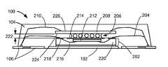
- FIG. 1therein is shown a bottom view of a stacked integrated circuit package system 100 in an embodiment of the present invention.
- the bottom viewdepicts a paddle 102 , such as a die-attach paddle, surrounded by a package encapsulation 104 , such as an epoxy mold compound.
- the package encapsulation 104preferably surrounds and exposes dual rows of external interconnects 106 , such as leads.
- the external interconnects 106preferably surround the paddle 102 .
- the stacked integrated circuit package system 100is shown having the paddle 102 , although it is understood that the stacked integrated circuit package system 100 may not have the paddle 102 .
- the external interconnects 106are shown in a dual row configuration, although it is understood that the external interconnects 106 may be in a different configuration, such as a single row or more than dual rows of the external interconnects 106 .
- the dual rows of the external interconnects 106are shown in a staggered configuration, although it is understood that the external interconnects 106 may not be staggered from row to row.
- FIG. 2therein is shown a cross-sectional view of the stacked integrated circuit package system 100 along a line 2 - 2 of FIG. 1 .
- the stacked integrated circuit package system 100is shown as an integrated circuit package-in-package system.
- the cross-sectional viewdepicts the paddle 102 between the external interconnects 106 .
- a first device 202such as an integrated circuit package system having a non-active side, is preferably over the paddle 102 and preferably connects to the external interconnects 106 with first interconnects 204 , such as bond wires or ribbon bonds.
- a “non-active side” for a packageis defined as a side of the package not having active integrated circuit components directly under the surface as would be the case for an active side of an integrated circuit die.
- a conductive spacer structure 206is preferably above the non-active side of the first device 202 and below a second device 208 , such as an integrated circuit die, wherein the second device 208 is over the first device 202 .
- Second interconnects 210preferably connect the second device 208 and the external interconnects 106 .
- the package encapsulation 104preferably covers the first device 202 , the first interconnects 204 , the second device 208 , and the second interconnects 210 over the paddle 102 and the external interconnects 106 .
- the package encapsulation 104exposes the external interconnects 106 and the paddle 102 to ambient.
- the first device 202includes an integrated circuit die 212 attached to a mounting structure 214 , such as a die-attach paddle.
- Inner interconnects 216such as bond wires, connect the integrated circuit die 212 and terminals 218 , such as bond pads, of the first device 202 .
- An inner encapsulation 220such as an epoxy mold compound, covers the integrated circuit die 212 and the inner interconnects 216 over the mounting structure 214 and the terminals 218 .
- the inner encapsulation 220exposes the mounting structure 214 and the terminals 218 on a non-active side for further connections.
- the first device 202is shown as having the mounting structure 214 , although it is understood that the first device 202 may not have the mounting structure 214 .
- the integrated circuit die 212is shown as a wire bonded integrated circuit, although it is understood that the integrated circuit die 212 may not be a wire bonded integrated circuit, such as a flip chip.
- the conductive spacer structure 206is directly on the mounting structure 214 providing a space 222 between the first device 202 and the second device 208 for the first interconnects 204 to connect to the terminals 218 .
- the conductive spacer structure 206may be used as test points for the first device 202 ensuring known good device (KGD) without assembly of the stacked integrated circuit package system 100 .
- the mounting structure 214may be connected to the integrated circuit die 212 and the conductive spacer structure 206 is connected to the mounting structure 214 .
- the mounting structure 214may include conductive traces (not shown) or routes (not shown) for providing a redistribution layer or a patterned circuit layer.
- the first device 202may be tested using the terminals 218 and the conductive spacer structure 206 .
- the second device 208includes a non-active side 224 and an active side 226 having active circuitry fabricated thereon.
- the second device 208is shown facing up with the non-active side 224 facing the first device 202 and the conductive spacer structure 206 .
- the conductive spacer structure 206can be directly attached to the non-active side 224 of the second device 208 .
- the second interconnects 210connect with the active side 226 .
- the conductive spacer structure 206is shown serving a spacer function between the first device 202 and the second device 208 , although it is understood that the conductive spacer structure 206 may serve other functions, such as conductive terminals between the first device 202 and the second device 208 or heat dissipation structure.
- FIG. 3therein is shown a more detailed cross-sectional view the conductive spacer structure 206 of FIG. 1 .
- the more detailed cross-sectional viewdepicts the conductive spacer structure 206 between the first device 202 and the second device 208 .
- the first device 202has the mounting structure 214 and the terminals 218 .
- the conductive spacer structure 206includes conductive elements 302 , such as bumps, balls, or posts of metal or metallic alloy, surrounded by a spacer filler 304 , such as dispensed epoxy.
- the conductive elements 302may serve a number of functions. For example, the conductive elements 302 may provide test points for the first device 202 , may provide heat dissipation path, or may serve as communication paths between the first device 202 and the second device 208 , to name a few.
- the conductive elements 302 with the spacer filler 304provides the space 222 to be more uniform between the first device 202 and the second device 208 allowing for a consistent bondline thickness (BLT).
- the conductive elements 302may be formed by stacking a number of levels of the conductive elements 302 allowing an improved control of the space 222 between the first device 202 and the second device 208 .
- the conductive elements 302 in the spacer filler 304also allow the conductive spacer structure 206 to mitigate or to eliminate tilting of the second device 208 during assembly of the stacked integrated circuit package system 100 .
- the conductive spacer structure 206provides cost reduction by enabling use of lower cost material for the spacer filler 304 .
- the spacer filler 304such as an epoxy resin with silica, aluminum nitride, nitride particle, or other polymeric materials, may insulate the conductive elements 302 from each other.
- the spacer filler 304may be conductive comprised of silver particle filled epoxy resin.
- An example of a higher cost materialis an epoxy resin with a controlled, large diameter filler particle size, such as silver balls or spherical silica.
- FIG. 4therein is shown a plan view of the conductive spacer structure 206 of FIG. 1 .
- the plan viewdepicts a portion of the stacked integrated circuit package system 100 of FIG. 1 without the package encapsulation 104 of FIG. 1 and over the paddle 102 .
- the plan viewdepicts the second device 208 over the paddle 102 .
- the spacer filler 304is shown within the boundary of the second device 208 .
- the conductive elements 302are depicted as dotted circles in a fully distributed array configuration below the second device 208 .
- FIG. 5therein is shown a plan view of a conductive spacer structure 500 in an alternative embodiment of the present invention.
- the conductive spacer structure 500may be the conductive spacer structure 206 of FIG. 2 in the stacked integrated circuit package system 100 of FIG. 1 .
- the plan viewdepicts a portion of the stacked integrated circuit package system 100 without the package encapsulation 104 of FIG. 1 and over the paddle 102 .
- the plan viewdepicts the second device 208 over the paddle 102 .
- the spacer filler 304is shown within the boundary of the second device 208 .
- the conductive elements 302are depicted as dotted circles in a center array configuration below the second device 208 .
- FIG. 6therein is shown is a plan view of a conductive spacer structure 600 in another alternative embodiment of the present invention.
- the conductive spacer structure 600may be the conductive spacer structure 206 of FIG. 2 in the stacked integrated circuit package system 100 of FIG. 1 .
- the plan viewdepicts a portion of the stacked integrated circuit package system 100 without the package encapsulation 104 of FIG. 1 and over the paddle 102 .
- the plan viewdepicts the second device 208 over the paddle 102 .
- the spacer filler 304is shown within the boundary of the second device 208 .
- the conductive elements 302are depicted as dotted circles in a peripheral configuration below the second device 208 .
- the conductive spacer structure 206may be formed in different configurations, such as those illustrated in FIG. 4 , FIG. 5 , and FIG. 6 .
- the conductive spacer structure 206also may be formed in a symmetrical and asymmetrical configuration.
- FIG. 7therein is shown a cross-sectional view of a stacked integrated circuit package system 700 along a line 2 - 2 of FIG. 1 in an alternative embodiment of the present invention.
- the bottom view of the stacked integrated circuit package system 100 of FIG. 1may also represent the bottom view of the stacked integrated circuit package system 700 .
- the stacked integrated circuit package system 700is shown as an integrated circuit package-in-package system.
- the cross-sectional viewdepicts the paddle 102 between the external interconnects 106 .
- a first device 702such as an integrated circuit package system, is preferably over the paddle 102 and preferably connects to the external interconnects 106 with first interconnects 704 , such as bond wires or ribbon bonds.
- a conductive spacer structure 706is preferably between the first device 702 and a second device 708 , such as an integrated circuit package system, wherein the second device 708 is over the first device 702 .
- Second interconnects 710preferably connect the second device 708 and the external interconnects 106 .
- the package encapsulation 104preferably covers the first device 702 , the first interconnects 704 , the second device 708 , and the second interconnects 710 over the paddle 102 and the external interconnects 106 .
- the package encapsulation 104also exposes the external interconnects 106 and the paddle 102 to ambient.
- the first device 702is shown as having the first mounting structure 714 , although it is understood that the first device 702 may not have the first mounting structure 714 .
- the first integrated circuit die 712is shown as a wire bonded integrated circuit, although it is understood that the first integrated circuit die 712 may not be a wire bonded integrated circuit, such as a flip chip.
- the conductive spacer structure 706is over the first mounting structure 714 providing a space 722 between the first device 702 and the second device 708 for the first interconnects 704 to connect to the first terminals 718 .
- the conductive spacer structure 706may be used as test points for the first device 702 ensuring known good device (KGD) without assembly of the stacked integrated circuit package system 700 .
- the first mounting structure 714may be connected to the first integrated circuit die 712 and the conductive spacer structure 706 is connected to the first mounting structure 714 .
- the first mounting structure 714may include conductive traces (not shown) or routes (not shown) for providing a redistribution layer or a patterned circuit layer.
- the first device 702may be tested using the first terminals 718 and the conductive spacer structure 706 .
- the second device 708includes a second integrated circuit die 724 attached to a second mounting structure 726 , such as a die-attach paddle.
- Second inner interconnects 728such as bond wires, connect the second integrated circuit die 724 and second terminals 732 , such as bond pads, of the second device 708 .
- a second inner encapsulation 730such as an epoxy mold compound, covers the second integrated circuit die 724 and the second inner interconnects 728 over the second mounting structure 726 and the second terminals 732 .
- the second inner encapsulation 730exposes the second mounting structure 726 and the second terminals 732 for further connections.
- the second device 708is shown as having the second mounting structure 726 , although it is understood that the second device 708 may not have the second mounting structure 726 .
- the second integrated circuit die 724is shown as a wire bonded integrated circuit, although it is understood that the second integrated circuit die 724 may not be a wire bonded integrated circuit, such as a flip chip.
- the first device 702 and the second device 708are shown as substantially the same, although it is understood that the first device 702 and the second device 708 may be different, such as different sizes or functions.
- the second device 708has the second terminals 732 facing away from the conductive spacer structure 706 , although it is understood that the second device 708 may have the second terminals 732 facing the conductive spacer structure 706 .
- the conductive spacer structure 706is shown serving a spacer function between the first device 702 and the second device 708 , although it is understood that the conductive spacer structure 706 may serve other functions, such as conductive terminals between the first device 702 and the second device 708 or heat dissipation structure.
- FIG. 8therein is shown a bottom view of a stacked integrated circuit package system 800 in another alternative embodiment of the present invention.
- the bottom viewdepicts a package carrier 802 , such as a laminated substrate, having external interconnects 806 , such as solder balls, thereon.
- the external interconnects 806are shown as in an array configuration, although it is understood that the external interconnects 806 may be in a different configuration, such as a peripheral configuration. Also for illustrative purposes, the external interconnects 806 are shown as solder balls, although it is understood that the external interconnects 806 may be different connection structures, such as bond pads or exposed leads.
- FIG. 9therein is shown a cross-sectional view of the stacked integrated circuit package system 800 along a line 9 - 9 of FIG. 8 .
- the stacked integrated circuit package system 800is shown as an integrated circuit package-in-package system.
- the cross-sectional viewdepicts the package carrier 802 over the external interconnects 806 .
- a first device 902such as an integrated circuit package system, is preferably over the package carrier 802 and preferably connects to the package carrier 802 with first interconnects 904 , such as bond wires or ribbon bonds.
- a conductive spacer structure 906is preferably between the first device 902 and a second device 908 , such as an integrated circuit die, wherein the second device 908 is over the first device 902 .
- Second interconnects 910preferably connect the second device 908 and the external interconnects 806 .
- the package carrier 802may function as a redistribution layer routing signals between the first device 902 , the second device 908 , and the external interconnects 806 .
- a package encapsulation 911preferably covers the first device 902 , the first interconnects 904 , the second device 908 , and the second interconnects 910 over the package carrier 802 .
- the package encapsulation 911exposes a side of the package carrier 802 opposite the side facing the first device 902 .
- the first device 902includes an integrated circuit die 912 attached to a mounting structure 914 , such as a die-attach paddle.
- Inner interconnects 916such as bond wires, connect the integrated circuit die 912 and terminals 918 , such as bond pads, of the first device 902 .
- An inner encapsulation 920such as an epoxy mold compound, covers the integrated circuit die 912 and the inner interconnects 916 over the mounting structure 914 and the terminals 918 .
- the inner encapsulation 920exposes the mounting structure 914 and the terminals 918 on a non-active side for further connections.
- the first device 902is shown as having the mounting structure 914 , although it is understood that the first device 902 may not have the mounting structure 914 .
- the integrated circuit die 912is shown as a wire bonded integrated circuit, although it is understood that the integrated circuit die 912 may not be a wire bonded integrated circuit, such as a flip chip.
- the conductive spacer structure 906is over the mounting structure 914 providing a space 922 between the first device 902 and the second device 908 for the first interconnects 904 to connect to the terminals 918 .
- the conductive spacer structure 906may be used as test points for the first device 902 ensuring known good device (KGD) without assembly of the stacked integrated circuit package system 800 .
- the mounting structure 914may be connected to the integrated circuit die 912 and the conductive spacer structure 906 is connected to the mounting structure 914 .
- the mounting structure 914may include conductive traces (not shown) or routes (not shown) for providing a redistribution layer or a patterned circuit layer.
- the first device 902may be tested using the terminals 918 and the conductive spacer structure 906 .
- the second device 908includes a non-active side 924 and an active side 926 having active circuitry fabricated thereon.
- the second device 908is shown facing up with the non-active side 924 facing the first device 902 and the conductive spacer structure 906 .
- the second interconnects 910connect with the active side 926 .
- the second device 908is shown as a wire bonded integrated circuit, although it is understood that the second device 908 may not be a wire bonded integrated circuit, such as a flip chip. Also for illustrative purposes, the second device 908 has the non-active side 924 facing the conductive spacer structure 906 , although it is understood that the second device 908 may have the active side 926 facing the conductive spacer structure 906 .
- the conductive spacer structure 906is shown serving a spacer function between the first device 902 and the second device 908 , although it is understood that the conductive spacer structure 906 may serve other functions, such as conductive terminals between the first device 902 and the second device 908 or heat dissipation structure.
- FIG. 10therein is shown a cross-sectional view of a stacked integrated circuit package system 1000 along a line 9 - 9 of FIG. 8 in yet another alternative embodiment of the present invention.
- the bottom view of the stacked integrated circuit package system 800 of FIG. 8may also represent the bottom view of the stacked integrated circuit package system 1000 .
- the stacked integrated circuit package system 1000is shown as an integrated circuit package-in-package system.
- the cross-sectional viewdepicts the package carrier 802 , such as a laminated substrate, over the external interconnects 806 , such as solder balls.
- a first device 1002such as an integrated circuit package system, is preferably over the package carrier 802 and preferably connects to the package carrier 802 with first interconnects 1004 , such as bond wires or ribbon bonds.
- a conductive spacer structure 1006is preferably between the first device 1002 and a second device 1008 , such as an integrated circuit package system, wherein the second device 1008 is over the first device 1002 .
- Second interconnects 1010preferably connect the second device 1008 and the package carrier 802 .
- the package carrier 802may function as a redistribution layer routing signals between the first device 1002 , the second device 1008 , and the external interconnects 806 .
- a package encapsulation 1011preferably covers the first device 1002 , the first interconnects 1004 , the second device 1008 , and the second interconnects 1010 over the package carrier 802 .
- the package encapsulation 1011exposes a side of the package carrier 802 opposite the side facing the first device 1002 .
- the first device 1002includes a first integrated circuit die 1012 attached to a first substrate 1014 , such as a laminated substrate.
- the first substrate 1014preferably provides a redistribution layer for communication between the first integrated circuit die 1012 and the first interconnects 1004 .
- First inner interconnects 1016such as bond wires, connect the first integrated circuit die 1012 and the first substrate 1014 .
- the first integrated circuit die 1012is shown as a wire bonded integrated circuit, although it is understood that the first integrated circuit die 1012 may not be a wire bonded integrated circuit, such as a flip chip.
- a first inner encapsulation 1020such as an epoxy mold compound, covers the first integrated circuit die 1012 and the first inner interconnects 1016 over the first substrate 1014 .
- the first inner encapsulation 1020exposes the first substrate 1014 on a non-active side for further connections.
- the conductive spacer structure 1006is over the first substrate 1014 providing a space 1022 between the first device 1002 and the second device 1008 for the first interconnects 1004 to connect to the first substrate 1014 .
- the conductive spacer structure 1006may be used as test points for the first device 1002 ensuring known good device (KGD) without assembly of the stacked integrated circuit package system 1000 .
- the first substrate 1014may be connected to the first integrated circuit die 1012 and the conductive spacer structure 1006 is connected to the first substrate 1014 .
- the first device 1002may be tested using the first substrate 1014 and the conductive spacer structure 1006 .
- the second device 1008includes a second integrated circuit die 1024 attached to a second substrate 1026 , such as a laminated substrate.
- the second substrate 1026preferably provides a redistribution layer for communication between the second integrated circuit die 1024 and the second interconnects 1010 .
- Second inner interconnects 1030such as bond wires, connect the second integrated circuit die 1024 and the second substrate 1026 .
- the second integrated circuit die 1024is shown as a wire bonded integrated circuit, although it is understood that the second integrated circuit die 1024 may not be a wire bonded integrated circuit, such as a flip chip.
- the first device 1002 and the second device 1008are shown as substantially the same, although it is understood that the first device 1002 and the second device 1008 may be different, such as different sizes or functions.
- the second device 1008has the second substrate 1026 facing away from the conductive spacer structure 1006 , although it is understood that the second device 1008 may have the second substrate 1026 facing the conductive spacer structure 1006 .
- the conductive spacer structure 1006is shown serving a spacer function between the first device 1002 and the second device 1008 , although it is understood that the conductive spacer structure 1006 may serve other functions, such as conductive terminals between the first device 1002 and the second device 1008 or heat dissipation structure.
- FIG. 11therein is shown a cross-sectional view of the stacked integrated circuit package system 700 of FIG. 7 in a phase attaching the first device 702 .
- the cross-sectional viewdepicts the paddle 102 between the external interconnects 106 .
- the first device 702attaches to the paddle 102 with an adhesive 1102 , such as an epoxy.
- the first mounting structure 714 and the first terminals 718are exposed and facing away from the paddle 102 .
- FIG. 12therein is shown the structure of FIG. 11 in a phase attaching the conductive elements 302 and the first interconnects 704 .
- the first device 702 over the paddle 102has the first mounting structure 714 and the first terminals 718 exposed for further connections.
- the conductive elements 302are formed on the first mounting structure 714 .
- the first interconnects 704connect the first terminals 718 and the external interconnects 106 .
- the conductive elements 302 and the first interconnects 704may be formed by a number different methods.
- the conductive elements 302 and the first interconnects 704may be formed with a single pass of the wire bonding cantilever to attach the first interconnects 704 and to place the conductive elements 302 on the first mounting structure 714 .
- FIG. 13therein is shown the structure of FIG. 12 in a phase dispensing the spacer filler 304 .
- the first device 702is over the paddle 102 .
- the first device 702also has the conductive elements 302 over the first mounting structure 714 .
- the first interconnects 704connect the first terminals 718 and the external interconnects 106 .
- the spacer filler 304is dispensed over the conductive elements 302 and the first mounting structure 714 .
- the spacer filler 304does not contaminate the first terminals 718 or the first interconnects 704 .
- FIG. 14therein is shown the structure of FIG. 13 in a phase attaching the second device 708 .
- the second device 708mounts over the first device 702 compressing the spacer filler 304 .
- the space 722 between the first device 702 and the second device 708is uniform from the support provided by the conductive elements 302 of the conductive spacer structure 706 .
- the conductive spacer structure 706provides the space 722 such that the second device 708 does not perturb the first interconnects 704 in the space 722 .
- FIG. 15therein is shown the structure of FIG. 14 in a phase attaching the second interconnects 710 .
- the second device 708stacks over the first device 702 with the conductive spacer structure 706 in between.
- the second interconnects 710connect the second terminals 732 and the external interconnects 106 with the conductive spacer structure 706 mitigating or eliminating tilt of the second device 708 .
- FIG. 16therein is shown the structure of FIG. 15 in a phase molding the package encapsulation 104 .
- the package encapsulation 104is preferably molded covering the first device 702 , the first interconnects 704 , the second device 708 , and the second interconnects 710 over the paddle 102 and the external interconnects 106 .
- the package encapsulation 104also exposes the external interconnects 106 and the paddle 102 to ambient.
- the molding processforms the stacked integrated circuit package system 700 .
- Yet other important aspects of the embodimentsinclude that it valuably supports and services the historical trend of reducing costs, simplifying systems, and increasing performance.
- the stacked integrated circuit package system of the present inventionfurnishes important and heretofore unknown and unavailable solutions, capabilities, and functional aspects for improving reliability in systems.
- the resulting processes and configurationsare straightforward, cost-effective, uncomplicated, highly versatile, and effective, can be implemented by adapting known technologies, and are thus readily suited for efficiently and economically manufacturing stacked integrated circuit package system.
Landscapes
- Engineering & Computer Science (AREA)
- Power Engineering (AREA)
- Microelectronics & Electronic Packaging (AREA)
- Physics & Mathematics (AREA)
- Condensed Matter Physics & Semiconductors (AREA)
- General Physics & Mathematics (AREA)
- Computer Hardware Design (AREA)
- Structures Or Materials For Encapsulating Or Coating Semiconductor Devices Or Solid State Devices (AREA)
Abstract
Description
Claims (10)
Priority Applications (1)
| Application Number | Priority Date | Filing Date | Title |
|---|---|---|---|
| US11/694,927US8134227B2 (en) | 2007-03-30 | 2007-03-30 | Stacked integrated circuit package system with conductive spacer |
Applications Claiming Priority (1)
| Application Number | Priority Date | Filing Date | Title |
|---|---|---|---|
| US11/694,927US8134227B2 (en) | 2007-03-30 | 2007-03-30 | Stacked integrated circuit package system with conductive spacer |
Publications (2)
| Publication Number | Publication Date |
|---|---|
| US20080237825A1 US20080237825A1 (en) | 2008-10-02 |
| US8134227B2true US8134227B2 (en) | 2012-03-13 |
Family
ID=39792807
Family Applications (1)
| Application Number | Title | Priority Date | Filing Date |
|---|---|---|---|
| US11/694,927Active2027-04-02US8134227B2 (en) | 2007-03-30 | 2007-03-30 | Stacked integrated circuit package system with conductive spacer |
Country Status (1)
| Country | Link |
|---|---|
| US (1) | US8134227B2 (en) |
Cited By (2)
| Publication number | Priority date | Publication date | Assignee | Title |
|---|---|---|---|---|
| US20140008785A1 (en)* | 2012-07-05 | 2014-01-09 | Taiwan Semiconductor Manufacturing Company, Ltd. | Package Redistribution Layer Structure and Method of Forming Same |
| US20170170164A1 (en)* | 2015-12-09 | 2017-06-15 | Samsung Display Co., Ltd. | Integrated circuit assembly with heat spreader and method of making the same |
Families Citing this family (3)
| Publication number | Priority date | Publication date | Assignee | Title |
|---|---|---|---|---|
| US7868471B2 (en)* | 2007-09-13 | 2011-01-11 | Stats Chippac Ltd. | Integrated circuit package-in-package system with leads |
| US8426955B2 (en)* | 2009-06-12 | 2013-04-23 | Stats Chippac Ltd. | Integrated circuit packaging system with a stack package and method of manufacture thereof |
| US8564111B2 (en) | 2011-01-27 | 2013-10-22 | Siano Mobile Silicon Ltd. | Stacked digital/RF system-on-chip with integral isolation layer |
Citations (52)
| Publication number | Priority date | Publication date | Assignee | Title |
|---|---|---|---|---|
| US5233504A (en) | 1990-12-06 | 1993-08-03 | Motorola, Inc. | Noncollapsing multisolder interconnection |
| US5923090A (en) | 1997-05-19 | 1999-07-13 | International Business Machines Corporation | Microelectronic package and fabrication thereof |
| US6137164A (en)* | 1998-03-16 | 2000-10-24 | Texas Instruments Incorporated | Thin stacked integrated circuit device |
| US6288451B1 (en)* | 1998-06-24 | 2001-09-11 | Vanguard International Semiconductor Corporation | Flip-chip package utilizing a printed circuit board having a roughened surface for increasing bond strength |
| US20020164838A1 (en)* | 2001-05-02 | 2002-11-07 | Moon Ow Chee | Flexible ball grid array chip scale packages and methods of fabrication |
| US20030038356A1 (en)* | 2001-08-24 | 2003-02-27 | Derderian James M | Semiconductor devices including stacking spacers thereon, assemblies including the semiconductor devices, and methods |
| US6528894B1 (en)* | 1996-09-20 | 2003-03-04 | Micron Technology, Inc. | Use of nitrides for flip-chip encapsulation |
| US6555917B1 (en)* | 2001-10-09 | 2003-04-29 | Amkor Technology, Inc. | Semiconductor package having stacked semiconductor chips and method of making the same |
| US6583512B2 (en)* | 2000-12-26 | 2003-06-24 | Matsushita Electric Industrial Co., Ltd. | Semiconductor device and method for fabricating the same |
| US6717253B2 (en)* | 2002-01-31 | 2004-04-06 | Advanced Semiconductor Engineering, Inc. | Assembly package with stacked dies and signal transmission plate |
| US20040121521A1 (en)* | 2002-07-31 | 2004-06-24 | Jackson Timothy L. | Semiconductor dice having back side redistribution layer accessed using through-silicon vias, methods of fabrication and assemblies |
| US20040126927A1 (en)* | 2001-03-05 | 2004-07-01 | Shih-Hsiung Lin | Method of assembling chips |
| US6762488B2 (en)* | 2002-03-19 | 2004-07-13 | Nec Electronics Corporation | Light thin stacked package semiconductor device and process for fabrication thereof |
| US6768190B2 (en)* | 2002-01-25 | 2004-07-27 | Advanced Semiconductor Engineering, Inc. | Stack type flip-chip package |
| US20040201088A1 (en)* | 2003-04-08 | 2004-10-14 | Samsung Electronics Co., Ltd. | Semiconductor multi-chip package and fabrication method |
| US6820329B2 (en)* | 2001-12-14 | 2004-11-23 | Advanced Semiconductor Engineering, Inc. | Method of manufacturing multi-chip stacking package |
| US20040238934A1 (en)* | 2001-08-28 | 2004-12-02 | Tessera, Inc. | High-frequency chip packages |
| US6833628B2 (en)* | 2002-12-17 | 2004-12-21 | Delphi Technologies, Inc. | Mutli-chip module |
| US20050006785A1 (en)* | 2002-06-04 | 2005-01-13 | Siliconware Precision Industries Co., Ltd. | Manufacturing method for multichip module |
| US6857470B2 (en)* | 2002-11-20 | 2005-02-22 | Samsung Electronics Co., Ltd. | Stacked chip package with heat transfer wires |
| US6870269B2 (en)* | 2001-10-15 | 2005-03-22 | Micron Technology, Inc. | Assemblies including stacked semiconductor devices separated a distance defined by adhesive material interposed therebetween, packages including the assemblies, and methods |
| US6885093B2 (en)* | 2002-02-28 | 2005-04-26 | Freescale Semiconductor, Inc. | Stacked die semiconductor device |
| US6894395B2 (en)* | 2002-02-13 | 2005-05-17 | Sony Corporation | System on a chip device including a re-wiring layer formed between groups of electronic devices |
| US20050110126A1 (en)* | 2003-11-25 | 2005-05-26 | Kai-Chiang Wu | Chip adhesive |
| US6921968B2 (en)* | 2003-05-02 | 2005-07-26 | Advance Semiconductor Engineering, Inc. | Stacked flip chip package |
| US6933176B1 (en) | 2002-07-19 | 2005-08-23 | Asat Ltd. | Ball grid array package and process for manufacturing same |
| US20050253240A1 (en)* | 2002-06-12 | 2005-11-17 | Wolfgang Nuechter | Micromechanical component and corresponsing production method |
| US20050258545A1 (en)* | 2004-05-24 | 2005-11-24 | Chippac, Inc. | Multiple die package with adhesive/spacer structure and insulated die surface |
| US20050269676A1 (en)* | 2004-05-24 | 2005-12-08 | Chippac, Inc | Adhesive/spacer island structure for stacking over wire bonded die |
| US6977439B2 (en) | 2002-03-21 | 2005-12-20 | Samsung Electronics Co., Ltd. | Semiconductor chip stack structure |
| US7005316B2 (en) | 2001-04-17 | 2006-02-28 | Micron Technology, Inc. | Method for package reduction in stacked chip and board assemblies |
| US7024947B2 (en)* | 2002-03-07 | 2006-04-11 | Alps Electric Co., Ltd. | Detection device including circuit component |
| US20060091562A1 (en)* | 2004-10-29 | 2006-05-04 | Hsin-Hui Lee | Flip chip BGA process and package with stiffener ring |
| US20060097402A1 (en)* | 2004-11-08 | 2006-05-11 | Siliconware Precision Industries Co., Ltd. | Semiconductor device having flip-chip package and method for fabricating the same |
| US20060197209A1 (en)* | 2005-02-10 | 2006-09-07 | Stats Chippac Ltd. | Stacked integrated circuits package system with dense routability and high thermal conductivity |
| US20060289980A1 (en)* | 2005-06-22 | 2006-12-28 | Chang Hong T | Stacked memory card and method for manufacturing the same |
| US7189593B2 (en)* | 2002-01-09 | 2007-03-13 | Micron Technology, Inc. | Elimination of RDL using tape base flip chip on flex for die stacking |
| US20070152313A1 (en)* | 2005-12-29 | 2007-07-05 | Shanggar Periaman | Stacked die semiconductor package |
| US7245003B2 (en)* | 2004-06-30 | 2007-07-17 | Intel Corporation | Stacked package electronic device |
| US20070194415A1 (en)* | 2006-02-20 | 2007-08-23 | Seng Eric T S | Semiconductor device assemblies including face-to-face semiconductor dice, systems including such assemblies, and methods for fabricating such assemblies |
| US20070216005A1 (en)* | 2006-03-17 | 2007-09-20 | Stats Chippac Ltd. | Integrated circuit package-in-package system |
| US20070257348A1 (en)* | 2006-05-08 | 2007-11-08 | Advanced Semiconductor Engineering, Inc. | Multiple chip package module and method of fabricating the same |
| US20070278657A1 (en)* | 2006-05-30 | 2007-12-06 | Samsung Electronics Co. Ltd. | Chip stack, method of fabrication thereof, and semiconductor package having the same |
| US20070284756A1 (en)* | 2006-06-12 | 2007-12-13 | Advanced Semiconductor Engineering, Inc. | Stacked chip package |
| US7309913B2 (en)* | 2003-01-23 | 2007-12-18 | St Assembly Test Services Ltd. | Stacked semiconductor packages |
| US20080042265A1 (en)* | 2006-08-15 | 2008-02-21 | Merilo Leo A | Chip scale module package in bga semiconductor package |
| US7355274B2 (en)* | 2004-12-10 | 2008-04-08 | Samsung Electronics Co., Ltd. | Semiconductor package, manufacturing method thereof and IC chip |
| US7420814B2 (en)* | 2004-10-07 | 2008-09-02 | Samsung Electronics Co., Ltd. | Package stack and manufacturing method thereof |
| US7435619B2 (en)* | 2006-02-14 | 2008-10-14 | Stats Chippac Ltd. | Method of fabricating a 3-D package stacking system |
| US20080280396A1 (en)* | 2005-02-22 | 2008-11-13 | Micron Technology, Inc. | Stacked die package for peripheral and center device pad layout device |
| US7518226B2 (en)* | 2007-02-06 | 2009-04-14 | Stats Chippac Ltd. | Integrated circuit packaging system with interposer |
| US20090174051A1 (en)* | 2004-01-22 | 2009-07-09 | Shuichi Osaka | Semiconductor package and semiconductor device |
- 2007
- 2007-03-30USUS11/694,927patent/US8134227B2/enactiveActive
Patent Citations (58)
| Publication number | Priority date | Publication date | Assignee | Title |
|---|---|---|---|---|
| US5233504A (en) | 1990-12-06 | 1993-08-03 | Motorola, Inc. | Noncollapsing multisolder interconnection |
| US6528894B1 (en)* | 1996-09-20 | 2003-03-04 | Micron Technology, Inc. | Use of nitrides for flip-chip encapsulation |
| US5923090A (en) | 1997-05-19 | 1999-07-13 | International Business Machines Corporation | Microelectronic package and fabrication thereof |
| US6137164A (en)* | 1998-03-16 | 2000-10-24 | Texas Instruments Incorporated | Thin stacked integrated circuit device |
| US6288451B1 (en)* | 1998-06-24 | 2001-09-11 | Vanguard International Semiconductor Corporation | Flip-chip package utilizing a printed circuit board having a roughened surface for increasing bond strength |
| US6583512B2 (en)* | 2000-12-26 | 2003-06-24 | Matsushita Electric Industrial Co., Ltd. | Semiconductor device and method for fabricating the same |
| US7242099B2 (en)* | 2001-03-05 | 2007-07-10 | Megica Corporation | Chip package with multiple chips connected by bumps |
| US20040126927A1 (en)* | 2001-03-05 | 2004-07-01 | Shih-Hsiung Lin | Method of assembling chips |
| US7005316B2 (en) | 2001-04-17 | 2006-02-28 | Micron Technology, Inc. | Method for package reduction in stacked chip and board assemblies |
| US20020164838A1 (en)* | 2001-05-02 | 2002-11-07 | Moon Ow Chee | Flexible ball grid array chip scale packages and methods of fabrication |
| US20030038356A1 (en)* | 2001-08-24 | 2003-02-27 | Derderian James M | Semiconductor devices including stacking spacers thereon, assemblies including the semiconductor devices, and methods |
| US7268426B2 (en)* | 2001-08-28 | 2007-09-11 | Tessera, Inc. | High-frequency chip packages |
| US20040238934A1 (en)* | 2001-08-28 | 2004-12-02 | Tessera, Inc. | High-frequency chip packages |
| US6555917B1 (en)* | 2001-10-09 | 2003-04-29 | Amkor Technology, Inc. | Semiconductor package having stacked semiconductor chips and method of making the same |
| US6870269B2 (en)* | 2001-10-15 | 2005-03-22 | Micron Technology, Inc. | Assemblies including stacked semiconductor devices separated a distance defined by adhesive material interposed therebetween, packages including the assemblies, and methods |
| US6820329B2 (en)* | 2001-12-14 | 2004-11-23 | Advanced Semiconductor Engineering, Inc. | Method of manufacturing multi-chip stacking package |
| US7189593B2 (en)* | 2002-01-09 | 2007-03-13 | Micron Technology, Inc. | Elimination of RDL using tape base flip chip on flex for die stacking |
| US6768190B2 (en)* | 2002-01-25 | 2004-07-27 | Advanced Semiconductor Engineering, Inc. | Stack type flip-chip package |
| US6717253B2 (en)* | 2002-01-31 | 2004-04-06 | Advanced Semiconductor Engineering, Inc. | Assembly package with stacked dies and signal transmission plate |
| US6894395B2 (en)* | 2002-02-13 | 2005-05-17 | Sony Corporation | System on a chip device including a re-wiring layer formed between groups of electronic devices |
| US6885093B2 (en)* | 2002-02-28 | 2005-04-26 | Freescale Semiconductor, Inc. | Stacked die semiconductor device |
| US7211466B2 (en)* | 2002-02-28 | 2007-05-01 | Freescale Semiconductor, Inc. | Stacked die semiconductor device |
| US7024947B2 (en)* | 2002-03-07 | 2006-04-11 | Alps Electric Co., Ltd. | Detection device including circuit component |
| US6762488B2 (en)* | 2002-03-19 | 2004-07-13 | Nec Electronics Corporation | Light thin stacked package semiconductor device and process for fabrication thereof |
| US6977439B2 (en) | 2002-03-21 | 2005-12-20 | Samsung Electronics Co., Ltd. | Semiconductor chip stack structure |
| US20050006785A1 (en)* | 2002-06-04 | 2005-01-13 | Siliconware Precision Industries Co., Ltd. | Manufacturing method for multichip module |
| US20050253240A1 (en)* | 2002-06-12 | 2005-11-17 | Wolfgang Nuechter | Micromechanical component and corresponsing production method |
| US6933176B1 (en) | 2002-07-19 | 2005-08-23 | Asat Ltd. | Ball grid array package and process for manufacturing same |
| US20040121521A1 (en)* | 2002-07-31 | 2004-06-24 | Jackson Timothy L. | Semiconductor dice having back side redistribution layer accessed using through-silicon vias, methods of fabrication and assemblies |
| US6857470B2 (en)* | 2002-11-20 | 2005-02-22 | Samsung Electronics Co., Ltd. | Stacked chip package with heat transfer wires |
| US6833628B2 (en)* | 2002-12-17 | 2004-12-21 | Delphi Technologies, Inc. | Mutli-chip module |
| US7309913B2 (en)* | 2003-01-23 | 2007-12-18 | St Assembly Test Services Ltd. | Stacked semiconductor packages |
| US20040201088A1 (en)* | 2003-04-08 | 2004-10-14 | Samsung Electronics Co., Ltd. | Semiconductor multi-chip package and fabrication method |
| US6921968B2 (en)* | 2003-05-02 | 2005-07-26 | Advance Semiconductor Engineering, Inc. | Stacked flip chip package |
| US20050110126A1 (en)* | 2003-11-25 | 2005-05-26 | Kai-Chiang Wu | Chip adhesive |
| US20090174051A1 (en)* | 2004-01-22 | 2009-07-09 | Shuichi Osaka | Semiconductor package and semiconductor device |
| US20050258545A1 (en)* | 2004-05-24 | 2005-11-24 | Chippac, Inc. | Multiple die package with adhesive/spacer structure and insulated die surface |
| US20050269676A1 (en)* | 2004-05-24 | 2005-12-08 | Chippac, Inc | Adhesive/spacer island structure for stacking over wire bonded die |
| US20070278645A1 (en)* | 2004-06-30 | 2007-12-06 | Intel Corporation | Stacked package electronic device |
| US7245003B2 (en)* | 2004-06-30 | 2007-07-17 | Intel Corporation | Stacked package electronic device |
| US7420814B2 (en)* | 2004-10-07 | 2008-09-02 | Samsung Electronics Co., Ltd. | Package stack and manufacturing method thereof |
| US20060091562A1 (en)* | 2004-10-29 | 2006-05-04 | Hsin-Hui Lee | Flip chip BGA process and package with stiffener ring |
| US20060097402A1 (en)* | 2004-11-08 | 2006-05-11 | Siliconware Precision Industries Co., Ltd. | Semiconductor device having flip-chip package and method for fabricating the same |
| US7355274B2 (en)* | 2004-12-10 | 2008-04-08 | Samsung Electronics Co., Ltd. | Semiconductor package, manufacturing method thereof and IC chip |
| US20060197209A1 (en)* | 2005-02-10 | 2006-09-07 | Stats Chippac Ltd. | Stacked integrated circuits package system with dense routability and high thermal conductivity |
| US20080280396A1 (en)* | 2005-02-22 | 2008-11-13 | Micron Technology, Inc. | Stacked die package for peripheral and center device pad layout device |
| US20060289980A1 (en)* | 2005-06-22 | 2006-12-28 | Chang Hong T | Stacked memory card and method for manufacturing the same |
| US7279795B2 (en)* | 2005-12-29 | 2007-10-09 | Intel Corporation | Stacked die semiconductor package |
| US20070152313A1 (en)* | 2005-12-29 | 2007-07-05 | Shanggar Periaman | Stacked die semiconductor package |
| US7435619B2 (en)* | 2006-02-14 | 2008-10-14 | Stats Chippac Ltd. | Method of fabricating a 3-D package stacking system |
| US20070194415A1 (en)* | 2006-02-20 | 2007-08-23 | Seng Eric T S | Semiconductor device assemblies including face-to-face semiconductor dice, systems including such assemblies, and methods for fabricating such assemblies |
| US20070216005A1 (en)* | 2006-03-17 | 2007-09-20 | Stats Chippac Ltd. | Integrated circuit package-in-package system |
| US20100230796A1 (en)* | 2006-03-17 | 2010-09-16 | Choong Bin Yim | Integrated circuit package-in-package system and method for making thereof |
| US20070257348A1 (en)* | 2006-05-08 | 2007-11-08 | Advanced Semiconductor Engineering, Inc. | Multiple chip package module and method of fabricating the same |
| US20070278657A1 (en)* | 2006-05-30 | 2007-12-06 | Samsung Electronics Co. Ltd. | Chip stack, method of fabrication thereof, and semiconductor package having the same |
| US20070284756A1 (en)* | 2006-06-12 | 2007-12-13 | Advanced Semiconductor Engineering, Inc. | Stacked chip package |
| US20080042265A1 (en)* | 2006-08-15 | 2008-02-21 | Merilo Leo A | Chip scale module package in bga semiconductor package |
| US7518226B2 (en)* | 2007-02-06 | 2009-04-14 | Stats Chippac Ltd. | Integrated circuit packaging system with interposer |
Cited By (4)
| Publication number | Priority date | Publication date | Assignee | Title |
|---|---|---|---|---|
| US20140008785A1 (en)* | 2012-07-05 | 2014-01-09 | Taiwan Semiconductor Manufacturing Company, Ltd. | Package Redistribution Layer Structure and Method of Forming Same |
| US9548283B2 (en)* | 2012-07-05 | 2017-01-17 | Taiwan Semiconductor Manufacturing Company, Ltd. | Package redistribution layer structure and method of forming same |
| US20170170164A1 (en)* | 2015-12-09 | 2017-06-15 | Samsung Display Co., Ltd. | Integrated circuit assembly with heat spreader and method of making the same |
| US9978663B2 (en)* | 2015-12-09 | 2018-05-22 | Samsung Display Co., Ltd. | Integrated circuit assembly with heat spreader and method of making the same |
Also Published As
| Publication number | Publication date |
|---|---|
| US20080237825A1 (en) | 2008-10-02 |
Similar Documents
| Publication | Publication Date | Title |
|---|---|---|
| US7368319B2 (en) | Stacked integrated circuit package-in-package system | |
| US7312519B2 (en) | Stacked integrated circuit package-in-package system | |
| US8232658B2 (en) | Stackable integrated circuit package system with multiple interconnect interface | |
| US20070241441A1 (en) | Multichip package system | |
| US7501697B2 (en) | Integrated circuit package system | |
| US7741707B2 (en) | Stackable integrated circuit package system | |
| US7420269B2 (en) | Stacked integrated circuit package-in-package system | |
| US8541872B2 (en) | Integrated circuit package system with package stacking and method of manufacture thereof | |
| US8729687B2 (en) | Stackable integrated circuit package system | |
| US8188586B2 (en) | Mountable integrated circuit package system with mounting interconnects | |
| US8143711B2 (en) | Integrated circuit package system with offset stacking and anti-flash structure | |
| US8536692B2 (en) | Mountable integrated circuit package system with mountable integrated circuit die | |
| US20070001296A1 (en) | Bump for overhang device | |
| US8026129B2 (en) | Stacked integrated circuits package system with passive components | |
| US7915724B2 (en) | Integrated circuit packaging system with base structure device | |
| US8247894B2 (en) | Integrated circuit package system with step mold recess | |
| US20090140408A1 (en) | Integrated circuit package-on-package system with stacking via interconnect | |
| US8012867B2 (en) | Wafer level chip scale package system | |
| US8093727B2 (en) | Integrated circuit package-in-package system with side-by-side and offset stacking and method for manufacturing thereof | |
| US20070096282A1 (en) | Integrated circuit package system including high-density small footprint system-in-package | |
| US8134227B2 (en) | Stacked integrated circuit package system with conductive spacer | |
| US7667314B2 (en) | Integrated circuit package system with mold lock subassembly | |
| US8956914B2 (en) | Integrated circuit package system with overhang die |
Legal Events
| Date | Code | Title | Description |
|---|---|---|---|
| AS | Assignment | Owner name:STATS CHIPPAC LTD., SINGAPORE Free format text:ASSIGNMENT OF ASSIGNORS INTEREST;ASSIGNORS:TAY, LIONEL CHIEN HUI;HUANG, RUI;CHOW, SENG GUAN;REEL/FRAME:019097/0987 Effective date:20070321 | |
| STCF | Information on status: patent grant | Free format text:PATENTED CASE | |
| AS | Assignment | Owner name:CITICORP INTERNATIONAL LIMITED, AS COMMON SECURITY AGENT, HONG KONG Free format text:SECURITY INTEREST;ASSIGNORS:STATS CHIPPAC, INC.;STATS CHIPPAC LTD.;REEL/FRAME:036288/0748 Effective date:20150806 Owner name:CITICORP INTERNATIONAL LIMITED, AS COMMON SECURITY Free format text:SECURITY INTEREST;ASSIGNORS:STATS CHIPPAC, INC.;STATS CHIPPAC LTD.;REEL/FRAME:036288/0748 Effective date:20150806 | |
| FPAY | Fee payment | Year of fee payment:4 | |
| AS | Assignment | Owner name:STATS CHIPPAC PTE. LTE., SINGAPORE Free format text:CHANGE OF NAME;ASSIGNOR:STATS CHIPPAC LTD.;REEL/FRAME:038378/0280 Effective date:20160329 | |
| MAFP | Maintenance fee payment | Free format text:PAYMENT OF MAINTENANCE FEE, 8TH YEAR, LARGE ENTITY (ORIGINAL EVENT CODE: M1552); ENTITY STATUS OF PATENT OWNER: LARGE ENTITY Year of fee payment:8 | |
| AS | Assignment | Owner name:STATS CHIPPAC, INC., CALIFORNIA Free format text:RELEASE BY SECURED PARTY;ASSIGNOR:CITICORP INTERNATIONAL LIMITED, AS COMMON SECURITY AGENT;REEL/FRAME:052879/0852 Effective date:20190503 Owner name:STATS CHIPPAC PTE. LTD. FORMERLY KNOWN AS STATS CHIPPAC LTD., SINGAPORE Free format text:RELEASE BY SECURED PARTY;ASSIGNOR:CITICORP INTERNATIONAL LIMITED, AS COMMON SECURITY AGENT;REEL/FRAME:052879/0852 Effective date:20190503 | |
| AS | Assignment | Owner name:STATS CHIPPAC PTE. LTE., SINGAPORE Free format text:CORRECT ERROR IN ASSIGNMENT NAME FROM STATS CHIPPAC PTE. LTE. TO STATS CHIPPAC PTE. LTD. (REEL: 38378 FRAME: 0280);ASSIGNOR:STATS CHIPPAC LTD.;REEL/FRAME:064789/0474 Effective date:20160329 | |
| AS | Assignment | Owner name:STATS CHIPPAC PTE. LTD., SINGAPORE Free format text:CORRECTIVE ASSIGNMENT TO CORRECT THE RECEIVING PARTY NAME PREVIOUSLY RECORDED AT REEL: 064789 FRAME: 0474 ASSIGNOR(S) HEREBY CONFIRMS THE CHANGE OF NAME;ASSIGNOR:STATS CHIPPAC LTD.;REEL/FRAME:064842/0046 Effective date:20160329 | |
| MAFP | Maintenance fee payment | Free format text:PAYMENT OF MAINTENANCE FEE, 12TH YEAR, LARGE ENTITY (ORIGINAL EVENT CODE: M1553); ENTITY STATUS OF PATENT OWNER: LARGE ENTITY Year of fee payment:12 |