US8134137B2 - Memory device constructions, memory cell forming methods, and semiconductor construction forming methods - Google Patents
Memory device constructions, memory cell forming methods, and semiconductor construction forming methodsDownload PDFInfo
- Publication number
- US8134137B2 US8134137B2US12/141,388US14138808AUS8134137B2US 8134137 B2US8134137 B2US 8134137B2US 14138808 AUS14138808 AUS 14138808AUS 8134137 B2US8134137 B2US 8134137B2
- Authority
- US
- United States
- Prior art keywords
- diode
- memory
- memory cell
- line
- current
- Prior art date
- Legal status (The legal status is an assumption and is not a legal conclusion. Google has not performed a legal analysis and makes no representation as to the accuracy of the status listed.)
- Active, expires
Links
- 230000015654memoryEffects0.000titleclaimsabstractdescription404
- 238000010276constructionMethods0.000titleclaimsabstractdescription79
- 238000000034methodMethods0.000titleclaimsdescription37
- 239000004065semiconductorSubstances0.000titleabstractdescription178
- 239000000463materialSubstances0.000claimsabstractdescription461
- 239000004020conductorSubstances0.000claimsdescription85
- 239000000758substrateSubstances0.000claimsdescription35
- 229920000642polymerPolymers0.000claimsdescription4
- 150000004770chalcogenidesChemical class0.000claimsdescription3
- 229910044991metal oxideInorganic materials0.000claimsdescription3
- 150000004706metal oxidesChemical class0.000claimsdescription3
- 229910052751metalInorganic materials0.000abstractdescription25
- 239000002184metalSubstances0.000abstractdescription25
- 125000006850spacer groupChemical group0.000description111
- 239000007769metal materialSubstances0.000description72
- 239000002019doping agentSubstances0.000description37
- 238000000151depositionMethods0.000description14
- 230000000873masking effectEffects0.000description13
- 230000008021depositionEffects0.000description12
- PXHVJJICTQNCMI-UHFFFAOYSA-NNickelChemical compound[Ni]PXHVJJICTQNCMI-UHFFFAOYSA-N0.000description10
- KDLHZDBZIXYQEI-UHFFFAOYSA-NPalladiumChemical compound[Pd]KDLHZDBZIXYQEI-UHFFFAOYSA-N0.000description10
- 229910052782aluminiumInorganic materials0.000description10
- XAGFODPZIPBFFR-UHFFFAOYSA-NaluminiumChemical compound[Al]XAGFODPZIPBFFR-UHFFFAOYSA-N0.000description10
- BASFCYQUMIYNBI-UHFFFAOYSA-NplatinumChemical compound[Pt]BASFCYQUMIYNBI-UHFFFAOYSA-N0.000description10
- XUIMIQQOPSSXEZ-UHFFFAOYSA-NSiliconChemical compound[Si]XUIMIQQOPSSXEZ-UHFFFAOYSA-N0.000description7
- 229910052710siliconInorganic materials0.000description7
- 239000010703siliconSubstances0.000description7
- ZXEYZECDXFPJRJ-UHFFFAOYSA-N$l^{3}-silane;platinumChemical compound[SiH3].[Pt]ZXEYZECDXFPJRJ-UHFFFAOYSA-N0.000description5
- NRTOMJZYCJJWKI-UHFFFAOYSA-NTitanium nitrideChemical compound[Ti]#NNRTOMJZYCJJWKI-UHFFFAOYSA-N0.000description5
- 238000005530etchingMethods0.000description5
- PCHJSUWPFVWCPO-UHFFFAOYSA-NgoldChemical compound[Au]PCHJSUWPFVWCPO-UHFFFAOYSA-N0.000description5
- 229910052737goldInorganic materials0.000description5
- 239000010931goldSubstances0.000description5
- 229910052738indiumInorganic materials0.000description5
- APFVFJFRJDLVQX-UHFFFAOYSA-Nindium atomChemical compound[In]APFVFJFRJDLVQX-UHFFFAOYSA-N0.000description5
- 229910052759nickelInorganic materials0.000description5
- 229910052763palladiumInorganic materials0.000description5
- 229910052697platinumInorganic materials0.000description5
- 229910021339platinum silicideInorganic materials0.000description5
- 229910021332silicideInorganic materials0.000description5
- FVBUAEGBCNSCDD-UHFFFAOYSA-Nsilicide(4-)Chemical compound[Si-4]FVBUAEGBCNSCDD-UHFFFAOYSA-N0.000description5
- VYPSYNLAJGMNEJ-UHFFFAOYSA-NSilicium dioxideChemical compoundO=[Si]=OVYPSYNLAJGMNEJ-UHFFFAOYSA-N0.000description4
- 230000015556catabolic processEffects0.000description4
- 230000001174ascending effectEffects0.000description3
- 229910005866GeSeInorganic materials0.000description2
- 229910002269La1–xCaxMnO3Inorganic materials0.000description2
- RTAQQCXQSZGOHL-UHFFFAOYSA-NTitaniumChemical compound[Ti]RTAQQCXQSZGOHL-UHFFFAOYSA-N0.000description2
- -1WOxInorganic materials0.000description2
- 238000000429assemblyMethods0.000description2
- 230000000712assemblyEffects0.000description2
- 229910017052cobaltInorganic materials0.000description2
- 239000010941cobaltSubstances0.000description2
- GUTLYIVDDKVIGB-UHFFFAOYSA-Ncobalt atomChemical compound[Co]GUTLYIVDDKVIGB-UHFFFAOYSA-N0.000description2
- 229910052732germaniumInorganic materials0.000description2
- GNPVGFCGXDBREM-UHFFFAOYSA-Ngermanium atomChemical compound[Ge]GNPVGFCGXDBREM-UHFFFAOYSA-N0.000description2
- 229910021421monocrystalline siliconInorganic materials0.000description2
- ZKATWMILCYLAPD-UHFFFAOYSA-Nniobium pentoxideChemical compoundO=[Nb](=O)O[Nb](=O)=OZKATWMILCYLAPD-UHFFFAOYSA-N0.000description2
- 150000004767nitridesChemical class0.000description2
- 235000012239silicon dioxideNutrition0.000description2
- 239000000377silicon dioxideSubstances0.000description2
- 229910052719titaniumInorganic materials0.000description2
- 239000010936titaniumSubstances0.000description2
- WFKWXMTUELFFGS-UHFFFAOYSA-NtungstenChemical compound[W]WFKWXMTUELFFGS-UHFFFAOYSA-N0.000description2
- 229910052721tungstenInorganic materials0.000description2
- 239000010937tungstenSubstances0.000description2
- HZNVUJQVZSTENZ-UHFFFAOYSA-N2,3-dichloro-5,6-dicyano-1,4-benzoquinoneChemical compoundClC1=C(Cl)C(=O)C(C#N)=C(C#N)C1=OHZNVUJQVZSTENZ-UHFFFAOYSA-N0.000description1
- SNLFYGIUTYKKOE-UHFFFAOYSA-N4-n,4-n-bis(4-aminophenyl)benzene-1,4-diamineChemical compoundC1=CC(N)=CC=C1N(C=1C=CC(N)=CC=1)C1=CC=C(N)C=C1SNLFYGIUTYKKOE-UHFFFAOYSA-N0.000description1
- 229910016411CuxOInorganic materials0.000description1
- 229910005829GeSInorganic materials0.000description1
- 229910052581Si3N4Inorganic materials0.000description1
- 229910002370SrTiO3Inorganic materials0.000description1
- 229910003087TiOxInorganic materials0.000description1
- 229910003134ZrOxInorganic materials0.000description1
- PNEYBMLMFCGWSK-UHFFFAOYSA-Naluminium oxideInorganic materials[O-2].[O-2].[O-2].[Al+3].[Al+3]PNEYBMLMFCGWSK-UHFFFAOYSA-N0.000description1
- 238000000137annealingMethods0.000description1
- 229910002113barium titanateInorganic materials0.000description1
- 229910052593corundumInorganic materials0.000description1
- 238000010586diagramMethods0.000description1
- 230000000694effectsEffects0.000description1
- GNBHRKFJIUUOQI-UHFFFAOYSA-NfluoresceinChemical compoundO1C(=O)C2=CC=CC=C2C21C1=CC=C(O)C=C1OC1=CC(O)=CC=C21GNBHRKFJIUUOQI-UHFFFAOYSA-N0.000description1
- 230000006870functionEffects0.000description1
- 238000012986modificationMethods0.000description1
- 230000004048modificationEffects0.000description1
- 230000002085persistent effectEffects0.000description1
- 238000005498polishingMethods0.000description1
- HQVNEWCFYHHQES-UHFFFAOYSA-Nsilicon nitrideChemical compoundN12[Si]34N5[Si]62N3[Si]51N64HQVNEWCFYHHQES-UHFFFAOYSA-N0.000description1
- 229910052709silverInorganic materials0.000description1
- 229910014031strontium zirconium oxideInorganic materials0.000description1
- PBCFLUZVCVVTBY-UHFFFAOYSA-Ntantalum pentoxideInorganic materialsO=[Ta](=O)O[Ta](=O)=OPBCFLUZVCVVTBY-UHFFFAOYSA-N0.000description1
- HLLICFJUWSZHRJ-UHFFFAOYSA-NtioxidazoleChemical compoundCCCOC1=CC=C2N=C(NC(=O)OC)SC2=C1HLLICFJUWSZHRJ-UHFFFAOYSA-N0.000description1
- 229910001845yogo sapphireInorganic materials0.000description1
Images


Classifications
- H—ELECTRICITY
- H10—SEMICONDUCTOR DEVICES; ELECTRIC SOLID-STATE DEVICES NOT OTHERWISE PROVIDED FOR
- H10N—ELECTRIC SOLID-STATE DEVICES NOT OTHERWISE PROVIDED FOR
- H10N70/00—Solid-state devices having no potential barriers, and specially adapted for rectifying, amplifying, oscillating or switching
- H10N70/011—Manufacture or treatment of multistable switching devices
- H10N70/021—Formation of switching materials, e.g. deposition of layers
- G—PHYSICS
- G11—INFORMATION STORAGE
- G11C—STATIC STORES
- G11C13/00—Digital stores characterised by the use of storage elements not covered by groups G11C11/00, G11C23/00, or G11C25/00
- G11C13/0002—Digital stores characterised by the use of storage elements not covered by groups G11C11/00, G11C23/00, or G11C25/00 using resistive RAM [RRAM] elements
- G11C13/0021—Auxiliary circuits
- G11C13/003—Cell access
- H—ELECTRICITY
- H10—SEMICONDUCTOR DEVICES; ELECTRIC SOLID-STATE DEVICES NOT OTHERWISE PROVIDED FOR
- H10B—ELECTRONIC MEMORY DEVICES
- H10B63/00—Resistance change memory devices, e.g. resistive RAM [ReRAM] devices
- H10B63/20—Resistance change memory devices, e.g. resistive RAM [ReRAM] devices comprising selection components having two electrodes, e.g. diodes
- H—ELECTRICITY
- H10—SEMICONDUCTOR DEVICES; ELECTRIC SOLID-STATE DEVICES NOT OTHERWISE PROVIDED FOR
- H10B—ELECTRONIC MEMORY DEVICES
- H10B63/00—Resistance change memory devices, e.g. resistive RAM [ReRAM] devices
- H10B63/80—Arrangements comprising multiple bistable or multi-stable switching components of the same type on a plane parallel to the substrate, e.g. cross-point arrays
- H—ELECTRICITY
- H10—SEMICONDUCTOR DEVICES; ELECTRIC SOLID-STATE DEVICES NOT OTHERWISE PROVIDED FOR
- H10D—INORGANIC ELECTRIC SEMICONDUCTOR DEVICES
- H10D8/00—Diodes
- H10D8/01—Manufacture or treatment
- H—ELECTRICITY
- H10—SEMICONDUCTOR DEVICES; ELECTRIC SOLID-STATE DEVICES NOT OTHERWISE PROVIDED FOR
- H10D—INORGANIC ELECTRIC SEMICONDUCTOR DEVICES
- H10D8/00—Diodes
- H10D8/60—Schottky-barrier diodes
- G—PHYSICS
- G11—INFORMATION STORAGE
- G11C—STATIC STORES
- G11C2213/00—Indexing scheme relating to G11C13/00 for features not covered by this group
- G11C2213/70—Resistive array aspects
- G11C2213/72—Array wherein the access device being a diode
- H—ELECTRICITY
- H10—SEMICONDUCTOR DEVICES; ELECTRIC SOLID-STATE DEVICES NOT OTHERWISE PROVIDED FOR
- H10B—ELECTRONIC MEMORY DEVICES
- H10B63/00—Resistance change memory devices, e.g. resistive RAM [ReRAM] devices
- H10B63/10—Phase change RAM [PCRAM, PRAM] devices
Definitions
- the present inventionin various embodiments, relates to memory device constructions, memory cell forming methods, and semiconductor construction forming methods.
- Resistive random access memoriesmay use a material capable of being configured in one of two different resistive states to store information. When configured in one of the resistive states, the material may have a high resistance to electrical current. In contrast, when configured in the other resistive state, the material may have a low resistance to electrical current.
- the resistive state in which the material is configuredmay be changed using electrical signals. For example, if the material is in a high-resistance state, the material may be configured to be in a low-resistance state by applying a voltage across the material.
- the resistive statemay be persistent. For example, once configured in a resistive state, the material may stay in the resistive state even if neither a current nor a voltage is applied to the material. Furthermore, the configuration of the material may be repeatedly changed from the high-resistance state to the low-resistance state or from the low-resistance state to the high-resistance state.
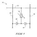
- FIG. 1is a schematic diagram of a memory device.
- FIGS. 2-4are diagrammatic, cross-sectional views of a portion of a semiconductor construction at various stages of an example embodiment process for forming memory cells.
- FIG. 5is a diagrammatic top view of a portion of a semiconductor construction of an example embodiment process for forming memory cells shown at the processing stage of FIG. 4 and illustrating the location of the portion of FIG. 4 along the line 4 - 4 .
- FIG. 6is a diagrammatic, cross-sectional view of the portion of FIG. 4 shown at a processing stage subsequent to that of FIG. 4 .
- the view of FIG. 7is along the line 7 - 7 of FIG. 6 .
- FIGS. 7-8are diagrammatic, cross-sectional views of a portion of a semiconductor construction at various stages of an example embodiment process for forming memory cells and illustrating the location of the portion of FIG. 6 along the line 6 - 6 .
- FIG. 9is a diagrammatic top view of the portion of FIG. 5 shown at a processing stage subsequent to that of FIG. 5 .
- the view of FIG. 8is along the line 8 - 8 of FIG. 9 and the view of FIG. 6 is along the line 6 - 6 of FIG. 9 .
- FIGS. 10-12are diagrammatic, cross-sectional views of the portion of FIG. 8 shown at processing stages subsequent to that of FIG. 8 .
- the view of FIG. 13is along the line 13 - 13 of FIG. 12 .
- FIG. 13is a diagrammatic, cross-sectional view of the portion of FIG. 6 shown at a processing stage subsequent to that of FIG. 6 .
- the view of FIG. 12is along the line 12 - 12 of FIG. 13 .
- FIGS. 14-15are diagrammatic, cross-sectional views of the portion of FIG. 12 shown at processing stages subsequent to that of FIG. 12 .
- the view of FIG. 6is along the lines 6 - 6 of FIGS. 14-15 .
- FIG. 16is a diagrammatic top view of the portion of FIG. 9 shown at a processing stage subsequent to that of FIG. 9 .
- the view of FIG. 15is along the line 15 - 15 of FIG. 16 and the view of FIG. 6 is along the line 6 - 6 of FIG. 16 .
- FIG. 17is a diagrammatic, cross-sectional view of the portion of FIG. 15 shown at a processing stage subsequent to that of FIG. 15 .
- the view of FIG. 18is along the line 18 - 18 of FIG. 17 .
- FIG. 18is a diagrammatic, cross-sectional view of the portion of FIG. 13 shown at a processing stage subsequent to that of FIG. 13 .
- the view of FIG. 17is along the line 17 - 17 of FIG. 18 .
- FIG. 19is a diagrammatic top view of the portion of FIG. 16 shown at a processing stage subsequent to that of FIG. 16 .
- the view of FIG. 17is along the line 17 - 17 of FIG. 19 and the view of FIG. 18 is along the line 18 - 18 of FIG. 19 .
- FIG. 20is a diagrammatic, cross-sectional view of a portion of a semiconductor construction of an example embodiment process for forming memory cells.
- FIGS. 21-22are diagrammatic, cross-sectional views of a portion of a semiconductor construction at various stages of an example embodiment process for forming memory cells.
- FIG. 23is a diagrammatic top view of a portion of a semiconductor construction of an example embodiment process for forming memory cells shown at the processing stage of FIG. 22 and illustrating the location of the portion of FIG. 22 along the line 22 - 22 .
- the view of FIG. 21is along the line 21 - 21 of FIG. 23 .
- FIGS. 24-27are diagrammatic, cross-sectional views of a portion of a semiconductor construction at various stages of an example embodiment process for forming memory cells.
- FIG. 28is a diagrammatic, cross-sectional view of the portion of FIG. 22 shown at a processing stage subsequent to that of FIG. 22 .
- the view of FIG. 27is along the line 27 - 27 of FIG. 28 .
- FIG. 29is a diagrammatic, cross-sectional view of the portion of FIG. 27 shown at a processing stage subsequent to that of FIG. 27 .
- FIG. 30is a diagrammatic top view of the portion of FIG. 23 shown at a processing stage subsequent to that of FIG. 23 .
- the view of FIG. 28is along the line 28 - 28 of FIG. 30 and the view of FIG. 29 is along the line 29 - 29 of FIG. 30 .
- FIG. 31is a diagrammatic, cross-sectional view of the portion of FIG. 29 shown at a processing stage subsequent to that of FIG. 29 .
- the view of FIG. 32is along the line 32 - 32 of FIG. 31 .
- FIG. 32is a diagrammatic, cross-sectional view of the portion of FIG. 28 shown at a processing stage subsequent to that of FIG. 28 .
- FIG. 33is a diagrammatic top view of the portion of FIG. 30 shown at a processing stage subsequent to that of FIG. 30 .
- the view of FIG. 31is along the line 31 - 31 of FIG. 33 and the view of FIG. 32 is along the line 32 - 32 of FIG. 33 .
- FIGS. 34-35are diagrammatic, cross-sectional views of a portion of a semiconductor construction at various stages of an example embodiment process for forming memory cells.
- FIG. 36is a diagrammatic top view of a portion of a semiconductor construction of an example embodiment process for forming memory cells.
- FIG. 36illustrates the location of the portion of FIG. 35 along the line 35 - 35 .
- FIGS. 37-44are diagrammatic, cross-sectional views of a portion of a semiconductor construction at various stages of an example embodiment process for forming memory cells.
- the view of FIG. 45is along the line 45 - 45 of FIGS. 42-44 .
- FIG. 45is a diagrammatic, cross-sectional view of the portion of FIG. 35 shown at a processing stage subsequent to that of FIG. 35 .
- the view of FIG. 44is along the line 44 - 44 of FIG. 45 .
- FIG. 46is a diagrammatic top view of the portion of FIG. 36 shown at a processing stage subsequent to that of FIG. 36 .
- Random access memoriesmay use resistive states of a memory element to store one or more bits of information.
- a memory element capable of being configured in either a high-resistance state or a low-resistance statemay store one bit of information by associating a bit value of “1” with the low-resistance state and a bit value of “0” with the high-resistance state.
- a bit value of “1”may be associated with the high-resistance state and a bit value of “0” may be associated with the low-resistance state.
- the memory elementmay include a bipolar memory material.
- a positive voltage applied across the bipolar memory materialmay change the configuration of the bipolar memory material from a high-resistance state to a low-resistance state.
- a negative voltage applied across the bipolar memory materialmay change the configuration of the bipolar memory material from a low-resistance state to a high-resistance state.
- a negative voltage applied across the bipolar memory materialmay change the configuration of the bipolar memory material from a high-resistance state to a low-resistance state and a positive voltage applied across the bipolar memory material may change the configuration of the bipolar memory material from a low-resistance state to a high-resistance.
- a bipolar memory materialmay be configured in a first resistive state using a voltage having a first polarity and may be configured in a second resistive state using a voltage having a polarity opposite that of the first polarity.
- bipolar memory materialexamples include ionic conducting chalcogenides, binary metal oxides, perovskite oxides, colossal magnetoresistives, and polymers.
- Example ionic conducting chalcogenides that may be used as bipolar memory materialinclude GeS, GeSe and Ag or Cu-doped GeS and GeSe.
- Example binary metal oxides that may be used as bipolar memory materialinclude HfOx, Nb2O5, Al2O3, WOx, Ta2O5, TiOx, ZrOx, CuxO, and NixO.
- Example ionic perovskite oxides that may be used as bipolar memory materialinclude doped or undoped SrTiO3, SrZrO3, BaTiO3.
- Example colossal magnetoresistives that may be used as bipolar memory materialinclude Pr1-xCaxMnO3 (PCMO), La1-xCaxMnO3 (LCMO), and Ba1-xSrxTiO3.
- Example polymers that may be used as bipolar memory materialinclude Bengala Rose, AlQ3Ag, Cu-TCNQ, DDQ, TAPA, and fluorescine-based polymers. Of course, other materials may be used as bipolar memory material. The materials listed above are provided by way of example rather than as an exhaustive list of bipolar memory material.
- a memory elementmay remain in the high-resistance state as long as a voltage greater than or equal to a turn-on voltage is not applied to the memory element.
- the memory elementmay remain in the high-resistance state even if no voltage is applied to the memory element. Accordingly, the high-resistance state of the memory element may be described as non-volatile since the high-resistance state might not change over time as long as a voltage greater than or equal to the turn-on voltage is not applied to the memory element.
- the memory elementmay remain in the low-resistance state as long as a voltage less than or equal to the turn-off voltage is not applied to the memory element.
- the memory elementmay remain in the low-resistance state even if no voltage is applied to the memory element.
- the low-resistance state of the memory elementmay also be described as non-volatile since the low-resistance state might not change over time as long as a voltage less than or equal to the turn-off voltage is not applied to the memory element.
- the memory elementmay be used to store one bit information.
- a memory elementmay represent a bit value of “0” when configured in the high-resistance state and may represent a bit value of “1” when configured in the low-resistance state.
- the resistive state of the memory elementmay be repeatedly changed over time. Accordingly, the memory element may be in the high-resistance state representing a bit value of “0” at one moment in time and the memory element may be in a low-resistance state representing a bit value of “1” at another moment in time.
- the representation of a bit value with resistance statescan be the opposite of that described above.
- Memory cell 10includes a memory element 14 , which may comprise a bipolar memory material such as one or more of the bipolar memory materials discussed above.
- Memory cell 10also includes a row line (e.g., a wordline) 12 , two column lines (e.g., bitlines) 18 and 20 , and two diodes 16 and 22 .
- Column line 20may be selectively electrically connected to memory element 14 .
- diode 22when diode 22 is forward biased (e.g., forward biased beyond a cut-in voltage of diode 22 ), diode 22 may conduct current from column line 20 to memory element 14 , thereby electrically connecting column line 20 to memory element 14 .
- diode 22when diode 22 is not forward biased (e.g., when diode 22 is reverse biased), diode 22 may hinder current from flowing from memory element 14 to column line 20 or from column line 20 to memory element 14 so that memory element 14 is not electrically connected to column line 20 .
- column line 18may be selectively electrically connected to memory element 14 .
- diode 16when diode 16 is forward biased (e.g., forward biased beyond a cut-in voltage of diode 16 ), diode 16 may conduct current from memory element 14 to column line 18 thereby electrically connecting memory element 14 to column line 18 .
- diode 16when diode 16 is not forward biased (e.g., when diode 16 is reverse biased), diode 16 may hinder current from flowing from column line 18 to memory element 14 or from memory element 14 to column line 18 so that memory element 14 is not electrically connected to column line 18 .
- Memory cell 10may store a bit of information via a resistive state of memory element 14 .
- the bitmay have a value of “0” or a value of “1.”
- the value of the bit stored by memory cell 10may be “0” and if memory element 14 is in a low-resistance state, the value of the bit stored by memory cell 10 may be “1.”
- a convention in which a high-resistance state represents a bit value of “1” and a low-resistance state represents a bit value of “0”may alternatively be used.
- a read operationmay be used to determine a value of a bit stored by memory cell 10 .
- a first positive voltagemay be applied between row line 12 and column line 18 so that row line 12 is at a higher potential than column line 18 and so that diode 16 is forward biased.
- the first positive voltagemay be greater than a cut-in voltage of diode 16 but less than a sum of the cut-in voltage of diode 16 and the turn-off voltage of memory element 14 so that the resistive state of memory element 14 is not altered.
- a second positive voltagemay be simultaneously applied between row line 12 and column line 20 so that row line 12 is at a higher potential than column line 20 and so that diode 22 is reverse biased.
- the second voltagemay be lower than a breakdown voltage of diode 22 .
- the first voltage and the second voltagemay be substantially the same voltage.
- memory element 14If memory element 14 is configured in a low-resistance state, current may flow from row line 12 through memory element 14 and forward-biased diode 16 to column line 18 . Based on the current, a memory device comprising memory cell 10 may determine that memory element 14 is in a low-resistance state and therefore the value stored by memory cell 10 is a “1.” For example, the memory device may compare the current on column line 18 with a reference current or the memory device may use the current on column line 18 to create a voltage and may then compare the voltage with a reference voltage.
- memory element 14may hinder current from flowing from row line 12 through memory element 14 and forward-biased diode 16 to column line 18 .
- memory element 14may restrict an amount of current flowing from row line 12 through memory element 14 and forward-biased diode 16 to column line 18 to a negligible amount of current that may be clearly distinguished from an amount of current allowed to flow when memory element 14 is in the low-resistance state.
- the memory device comprising memory cell 10may determine that memory element 14 is in the high-resistance state and therefore the value stored by memory cell 10 is a “0.”
- a first positive voltagemay be applied between column line 20 and row line 12 so that column line 20 is at a higher potential than row line 12 and so that diode 22 is forward biased.
- the first positive voltagemay be greater than the cut-in voltage of diode 22 but less than a sum of the cut-in voltage of diode 22 and the turn-on voltage of memory element 14 so that the resistive state of memory element 14 is not altered.
- a second positive voltagemay simultaneously be applied between column line 18 and row line 12 so that column line 18 is at a higher potential than row line 12 and so that diode 16 is reverse biased.
- the second voltagemay be lower than a breakdown voltage of diode 16 .
- the first voltage and the second voltagemay be substantially the same voltage.
- memory element 14If memory element 14 is configured in a low-resistance state, current may flow from column line 20 through forward-biased diode 22 and memory element 14 to row line 12 . Based on the current on row line 12 , a memory device comprising memory cell 10 may determine that memory element 14 is in a low-resistance state and therefore the value stored by memory cell 10 is a “1.”
- memory element 14may hinder current from flowing from column line 20 through forward-biased diode 22 and memory element 14 to row line 12 .
- memory element 14may restrict an amount of current flowing from column line 20 through forward-biased diode 22 and memory element 14 to row line 12 to a negligible amount that may be clearly distinguished from an amount of current allowed to flow when memory element 14 is in the low-resistance state.
- the memory device comprising memory cell 10may determine that memory element 14 is in the high-resistance state and therefore the value stored by memory cell 10 is a “0.”
- a bit valuemay be written to memory cell 10 .
- a first positive voltagemay be applied between column line 20 and row line 12 so that column line 20 is at a higher potential than row line 12 and so that diode 22 is forward biased.
- the first positive voltagemay be greater than a sum of the cut-in voltage of diode 22 and the turn-on voltage of memory element 14 . If memory element 14 is in a high-resistance state, the first voltage (or a current resulting from the first voltage) may re-configure memory element 14 to be in a low-resistance state.
- memory element 14may remain in the low-resistance state. Consequently, due to the first voltage, memory element 14 may be configured in a low-resistance state corresponding with a bit value of “1.”
- a second positive voltagemay be applied simultaneously with the first voltage.
- the second positive voltagemay be applied between column line 18 and row line 12 so that column line 18 is at a higher potential than row line 12 and so that diode 16 is reverse biased.
- the second voltagemay hinder current from flowing from column line 20 to column line 18 .
- the second voltagemay be lower than a breakdown voltage of diode 16 .
- the first voltagemay result from a first voltage pulse and the second voltage may result from a second voltage pulse.
- the first voltage and the second voltagemay be substantially the same voltage.
- a bit value of “0”may be written to memory cell 10 .
- a first positive voltagemay be applied between row line 12 and column line 18 so that row line 12 is at a higher potential than column line 18 and so that diode 16 is forward biased.
- the first positive voltagemay be greater than a sum of the cut-in voltage of diode 16 and the turn-off voltage of memory element 14 . If memory element 14 is in a low-resistance state, the first voltage (or a current resulting from the first voltage) may re-configure memory element 14 to be in a high-resistance state.
- memory element 14may remain in the high-resistance state. Consequently, due to the first voltage, memory element 14 may be configured in a high-resistance state corresponding with a bit value of “0.”
- a second positive voltagemay be applied simultaneously with the first voltage.
- the second positive voltagemay be applied between row line 12 and column line 20 so that row line 12 is at a higher potential than column line 20 and so that diode 22 is reverse biased.
- the second voltagemay hinder current from flowing from column line 18 to column line 20 .
- the second voltagemay be lower than a breakdown voltage of diode 22 .
- the first voltagemay result from a first voltage pulse and the second voltage may result from a second voltage pulse.
- the first voltage and the second voltagemay be substantially the same voltage.
- memory element 14may be re-written using these methods millions of times without damaging memory element 14 . Since memory element 14 may remain in a resistive state without a voltage or current being applied to memory element 14 as was discussed above, memory element 14 may be said to preserve a bit value in a non-volatile manner. Accordingly, memory cell 10 may store a bit of information without having to be frequently refreshed or memory cell 10 may be refreshed at a rate lower than a rate used to refresh a volatile memory cell.
- memory element 14is configured so that memory element 14 changes to a low-resistance state when a first voltage greater than the turn-on voltage of memory element 14 is applied across memory element 14 .
- the first voltagemay have a first polarity.
- the above discussionhas assumed that memory element 14 changes to a high-resistance state when a second voltage greater than the turn-off voltage of memory element 14 is applied across memory element 14 .
- the second voltagemay have a second polarity opposite that of the first polarity.
- memory element 14may be reversed so that memory element 14 changes to a high-resistance state when a voltage greater than the turn-off voltage of memory element 14 and having the first polarity is applied across memory element 14 .
- memory element 14may change to a low-resistance state when a voltage greater than the turn-on voltage of memory element 14 and having the second polarity is applied across memory element 14 .
- memory devicesmay be constructed based on an understanding that the high-resistance state of memory element 14 corresponds to a bit value of “1” and that the low-resistance state of memory element 14 corresponds to a bit value of “0” without changing the principles of writing and reading memory cell 10 .
- a memory elementhaving a high resistance state and a low resistance state.
- a memory elementmay be configurable in more than two different resistive states.
- Such a memory elementmay store more than one bit of information and may be used in a memory cell such as memory cell 10 .
- Each of a plurality of different programming voltagesmay correspond to a different one of a plurality of different resistive states of the memory element.
- the methods of programming memory cell 10 described abovemay be adapted to program a memory element having more than one resistive state by applying one of the plurality of programming voltages to the memory element in order to configure the memory element in the resistive state corresponding to the applied programming voltage. Furthermore, the methods of reading memory cell 10 described above may be adapted to read the memory element by comparing a current resulting from a voltage applied to the memory element to a plurality of different reference currents to determine in which of the plurality of different resistive states the memory cell is configured.
- Example embodiments of memory cellsare described below with reference to FIGS. 2-46 .
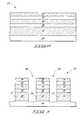
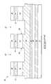
- construction 23includes a substrate 24 , and in ascending order from substrate 24 , an electrically conductive material 26 , a semiconductor material 28 , a metal material 30 , a memory material 32 , and a conductive material 34 .
- Substrate 24may comprise one or more of various semiconductor materials, such as silicon and germanium.
- Substrate 24can, for example, comprise, consist essentially of, or consist of monocrystalline silicon doped with background p-type dopant at a concentration of less than 10 16 atoms/cm 3 .
- the terms “semiconductive substrate,” “semiconductor construction,” and “semiconductor substrate”are defined to mean any construction comprising semiconductive material, including, but not limited to, bulk semiconductive materials such as a semiconductive wafer (either alone or in assemblies comprising other materials thereon), and semiconductive material layers (either alone or in assemblies comprising other materials).
- substraterefers to any supporting structure including, but not limited to, the semiconductive substrates described above.
- substrate 24may be an insulative material.
- Electrically conductive material 26may comprise any suitable composition, and may, for example, comprise, consist essentially of, or consist of silicon conductively doped with either n-type dopant or p-type dopant. In some embodiments, conductive material 26 may be silicon having a dopant concentration of 10 19 atoms/cm 3 or higher.
- Semiconductor material 28may comprise any suitable composition, and may, for example, comprise, consist essentially of, or consist of silicon lightly doped with either n-type dopant or p-type dopant.
- lightly dopedrefers to a material doped with a dopant at a concentration of between 10 16 and 10 19 atoms/cm 3 .
- semiconductor material 28may be lightly doped with an n-type dopant and metal material 30 may comprise any suitable composition, and may, for example, comprise, consist essentially of, or consist of platinum, palladium, titanium nitride, aluminum, gold, or nickel.
- semiconductor material 28may be lightly doped with a p-type dopant and metal material 30 may comprise any suitable composition, and may, for example, comprise, consist essentially of, or consist of platinum silicide, aluminum, or indium.
- Memory material 32may be a bipolar memory material as described above.
- Conductive material 34may comprise any suitable conductive composition, and may, for example, comprise, consist essentially of, or consist of metal or a conductively doped semiconductive material.
- Materials 26 , 28 , 30 , 32 , and 34may be deposited over substrate 24 , for example, as illustrated in FIG. 2 .
- Construction 23may be patterned using a masking material deposited over conductive material 34 to form trenches.
- etchingis conducted to form trenches 66 .
- the etchgoes through conductive material 34 , memory material 32 , metal material 30 , semiconductor material 28 , and conductive material 26 .
- the etchmay extend partially through substrate 24 .
- the etchmay be an anisotropic etch (e.g., a dry etch) and may, in some embodiments, comprise multiple different etches.
- conductive material 26may be formed into column lines 27 , 29 , and 31 .
- Column lines 27 , 29 , and 31may be electrically isolated from one another.
- Insulative material 36may be deposited on construction 23 .
- Insulative material 36may comprise any suitable insulative composition, and may, for example, comprise, consist essentially of, or consist of silicon dioxide.
- construction 23may be polished (e.g., using chemical-mechanical planarization (CMP)) to remove portions of insulative material 36 so that a top surface of metal material 34 is exposed while leaving insulative material 36 intact within trenches 66 .
- CMPchemical-mechanical planarization
- construction 23may be polished using CMP and the CMP may stop on metal material 34 .
- the CMPmay remove portions of insulative material 36 without removing significant portions of metal material 34 .
- metal material 34may prevent the CMP from removing portions of memory material 32 .
- metal material 34might not be included in construction 23 . Consequently, at the processing stage of FIG. 1 , memory material 32 may be the elevationally highest material above substrate 24 . In these embodiments, the CMP may stop on memory material 32 .
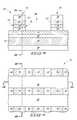
- FIG. 5is a diagrammatic top view of semiconductor construction 23 shown at the processing stage of FIG. 4 .
- the cross section of FIG. 4is shown along the line 4 - 4 of FIG. 5 .
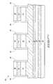
- an electrically conductive material 44is formed over metal material 34 and insulative material 36 .
- An insulative material 38is then formed over conductive material 44 .
- Conductive material 44may comprise one or more electrically conductive layers, and in some embodiments may comprise one or more metal-containing materials.
- the metal-containing materialsmay contain metal in elemental form (e.g., tungsten, titanium, etc.) and/or may contain metal as part of a composition (e.g., metal nitride, metal silicide, etc.).
- Insulative material 38may comprise any suitable insulative composition, and may, for example, comprise, consist essentially of, or consist of silicon nitride.
- FIG. 7is a cross-sectional view of construction 23 rotated ninety degrees with respect to FIG. 6 .
- Construction 23may be patterned using a masking material deposited over insulative material 38 in order to form trenches.
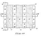
- construction 23 as illustrated in FIGS. 6-7is etched to form trench 68 and partially formed memory cells 70 and 72 .
- the etchgoes through insulative material 38 , conductive material 44 , metal material 34 , and memory material 32 and stops on metal material 30 .
- the etchmay be an anisotropic etch (e.g., a dry etch) and may, in some embodiments, comprise multiple different etches.
- partially formed memory cell 70has opposing vertical sidewalls 74 and 76 .
- conductive material 44may be formed into row lines 45 and 47 .
- row lines 45 and 47may be electrically isolated from each other.
- row lines 45 and 47extend horizontally into and out of the page and are above column lines 27 , 29 , and 31 .
- Column lines 27 , 29 , and 31also extend horizontally, but extend from left to right in FIG. 8 in a direction perpendicular to the horizontal extension of row lines 45 and 47 .
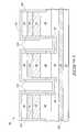
- FIG. 9is a diagrammatic top view of semiconductor construction 23 shown at the processing stage of FIG. 8 .
- the cross section of FIG. 8is shown along the line 8 - 8 of FIG. 9 and the cross section of FIG. 6 is shown along the line 6 - 6 of FIG. 9 .
- row lines 45 and 47are located underneath the lines of material 38 illustrated in FIG. 9 and extend horizontally.
- Column lines 27 , 29 , and 31are located underneath the lines of material 30 illustrated in FIG. 9 and extend vertically in a direction perpendicular to row lines 45 and 47 .
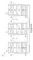
- insulative material 38is deposited over a top surface of construction 23 across partially formed memory cells 70 and 72 .
- the depositionmay be conformal so that insulative material 38 is in contact with sidewalls 74 and 76 and is over material 30 and the portions of insulative material 38 that were present prior to the deposition.
- An anisotropic etche.g., dry etch is then performed to form sidewall spacers.
- FIG. 11illustrates construction 23 of FIG. 10 subsequent to the anisotropic etch.
- horizontally extending portions of insulative material 38have been removed and vertically extending portions of insulative material 38 remain.
- the vertically extending portions of insulative material 38may be referred to as sidewall spacers 78 .
- two of sidewall spacers 78are in contact respectively with sidewalls 74 and 76 and are laterally adjacent to sidewalls 74 and 76 .
- metal material 40is deposited over the top surface of construction 23 in the processing stage illustrated in FIG. 11 .
- the depositionmay be conformal so that metal material 40 is in contact with sidewall spacers 78 and is over material 38 and material 30 .
- An anisotropic etchis then performed to form sidewall spacers.
- FIG. 14illustrates construction 23 of FIG. 12 subsequent to the anisotropic etch. Due to the etch, horizontally extending portions of insulative material 40 have been removed and vertically extending portions of insulative material 40 remain.
- the vertically extending portions of insulative material 40may be referred to as sidewall spacers 80 and may be in contact with sidewall spacers 78 and may be laterally adjacent to sidewall spacers 78 .
- an anisotropic etchmay be performed that etches through metal material 30 and semiconductor material 28 and partially through conductive material 26 to form trench 82 .
- the etchmay be selective for materials 30 , 28 , and 26 relative to materials 38 and 40 . Consequently, trench 82 may be self-aligned with sidewall spacers 80 since sidewall spacers 80 may determine the width of trench 82 .
- a series of etchesmay be performed to form trench 82 .
- a first etch selective for material 30may be performed followed by a second etch selective for material 28 followed by a third etch selective for material 26 .
- insulative material 36may be deposited on construction 23 thereby filling trench 82 .
- Construction 23may subsequently be polished to remove portions of insulative material 36 elevationally higher than a top surface of insulative material 38 .
- CMPmay be used to remove portions of insulative material 36 .
- the CMPmay stop on insulative material 38 and metal material 40 .
- the CMPmay remove portions of insulative material 36 without removing significant portions of insulative material 38 or metal material 40 .
- Semiconductor material 42may then be deposited on the polished surface so that semiconductor material 42 is in physical contact with insulative material 38 , sidewall spacers 78 and 80 , and insulative material 36 . Electrically conductive material 49 may then be deposited over, and in direct contact with, semiconductor material 42 .
- Conductive material 49may comprise one or more electrically conductive layers, and in some embodiments may comprise one or more metal-containing materials.
- the metal-containing materialsmay contain metal in elemental form (e.g., tungsten, titanium, etc.) and/or may contain metal as part of a composition (e.g., metal nitride, metal silicide, etc.).
- construction 23may be patterned using a masking material deposited over material 49 .
- An etche.g., an anisotropic etch
- portions 84 of construction 23are etched to remove materials 49 , 42 , and 40 while portions 86 of construction 23 are protected by the masking material.
- conductive material 49may be formed into column lines 51 , 53 , and 55 .
- column lines 51 , 53 , and 55may extend parallel to column lines 27 , 29 , and 31 .
- column lines 51 , 53 , and 55may be electrically isolated from each other.
- Each memory cellmay provide the functionality described above in relation to memory cell 10 of FIG. 1 .
- semiconductor material 28may be lightly doped with an n-type dopant and metal material 30 may comprise any suitable composition, and may, for example, comprise, consist essentially of, or consist of platinum, palladium, titanium nitride, aluminum, gold, or nickel.
- semiconductor material 42may be lightly doped with a p-type dopant and metal material 40 may comprise any suitable composition, and may, for example, comprise, consist essentially of, or consist of platinum silicide, aluminum, or indium.
- memory cell 46may implement the functionality of memory cell 10 of FIG. 1 (described above) as follows.
- Column lines 51 and 27may serve respectively as column lines 20 and 18 of FIG. 1
- row line 45may serve as row line 12
- memory material 32may serve as memory element 14 .
- a first one of sidewall spacers 80 of memory cell 46 and semiconductor material 42may form a Schottky diode that may serve as diode 22 of FIG. 1 with the one sidewall spacer 80 as a cathode of the diode and semiconductor material 42 as the anode of the diode.
- the other sidewall spacer 80 of memory cell 46may form a second Schottky diode (not illustrated in FIG. 1 ) connected in parallel with diode 22 and between column line 20 and memory element 14 .
- the anode of diode 22may be above row line 45 and above memory material 32 and the cathode of diode 22 (sidewall spacer 80 ) may extend vertically with a first portion elevationally higher than row line 45 and a second portion elevationally lower than row line 45 .
- a combination of metal material 30 of memory cell 46 and semiconductor material 28 of memory cell 46may serve as diode 16 of FIG. 1 with metal material 30 functioning as an anode and semiconductor material 28 functioning as a cathode.
- the amount of currentmay depend on a resistive state of memory material 32 and/or on a voltage applied across row line 45 and column line 27 . As was described above in relation to FIG. 1 , the current may be used, for example, to read memory cell 46 or to write a value to memory cell 46 .
- a currentmay flow from column line 51 through semiconductor material 42 , spacers 80 (which comprises metal material 40 ), metal material 30 , memory material 32 , and conductive material 34 to row line 45 .
- the currentmay flow through one or both of spacers 80 of memory cell 46 .
- the Schottky diode formed by metal material 40 and semiconductor material 42may conduct a current between column line 51 and row line 45 via memory material 32 .
- the amount of currentmay depend on a resistive state of memory material 32 and/or on a voltage applied across row line 45 and column line 51 . As was described above in relation to FIG. 1 , the current may be used, for example, to read memory cell 46 or to write a value to memory cell 46 .
- spacers 78insulate spacers 80 from row line 45 to prevent a short between the row line 45 and spacers 80 . Consequently, current may flow from spacers 80 to row line 45 via memory material 32 and may be prevented from flowing directly from spacers 80 to row line 45 by spacers 78 .
- semiconductor material 42may be lightly doped with an n-type dopant and metal material 40 may comprise any suitable composition, and may, for example, comprise, consist essentially of, or consist of platinum, palladium, titanium nitride, aluminum, gold, or nickel.
- semiconductor material 28may be lightly doped with a p-type dopant and metal material 30 may comprise any suitable composition, and may, for example, comprise, consist essentially of, or consist of platinum silicide, aluminum, or indium.
- memory cell 46may implement the functionality of memory cell 10 of FIG. 1 as described above in the previous embodiment except that the column lines and diodes are swapped.
- column lines 51 and 27may serve respectively as column lines 18 and 20 of FIG. 1 rather than respectively as column lines 20 and 18 .
- sidewall spacers 80 of memory cell 46 and semiconductor material 42may form Schottky diodes, one of which may serve as diode 16 of FIG. 1 , with sidewall spacers 80 as anodes of the diodes and semiconductor material 42 as the cathodes of the diodes.
- a combination of metal material 30 of memory cell 46 and semiconductor material 28 of memory cell 46may serve as diode 22 of FIG. 1 with metal material 30 functioning as a cathode and semiconductor material 28 functioning as an anode.
- a currentmay flow from column line 27 through semiconductor material 28 , metal material 30 , memory material 32 , and conductive material 34 to row line 45 .
- the currentmay be used, for example, to read memory cell 46 or to write a value to memory cell 46 .
- a currentmay flow from row line 45 through conductive material 34 , memory material 32 , metal material 30 , spacers 80 , and semiconductor material 42 to column line 51 .
- the currentmay flow through one or both of spacers 80 of memory cell 46 .
- the Schottky diode formed by metal material 40 and semiconductor material 42may conduct a current between column line 51 and row line 45 via memory material 32 .
- the currentmay be used, for example, to read memory cell 46 or to write a value to memory cell 46 .
- FIG. 20illustrates an embodiment of a semiconductor construction 101 in which semiconductor material 50 is used in place of metal material 30 and semiconductor material 54 is used in place of metal material 40 .
- conductive material 52is deposited between semiconductor material 50 and memory material 32 .
- semiconductor materials 42 and 50may be lightly doped with a p-type dopant and semiconductor materials 54 and 28 may be lightly doped with an n-type dopant.
- semiconductor materials 42 and 54together form a p/n semiconductor diode serving as diode 22 of FIG. 1 and semiconductor materials 50 and 28 together form a p/n semiconductor diode serving as diode 16 of FIG. 1 .
- semiconductor materials 42 and 50may be lightly doped with an n-type dopant and semiconductor materials 54 and 28 may be lightly doped with a p-type dopant.
- semiconductor materials 42 and 54together form a p/n semiconductor diode serving as diode 16 of FIG. 1 and semiconductor materials 50 and 28 together form a p/n semiconductor diode serving as diode 22 of FIG. 1 .
- conductive material 52may function as an electrode between the two diodes.
- conductive material 34might not be included in construction 101 if polishing may be performed without damaging memory material 32 (see the above discussion of FIGS. 3-4 ).
- memory cell 10Other physical embodiments of memory cell 10 are also possible.
- construction 56includes a substrate 13 , and in ascending order from substrate 13 , electrically conductive material 26 , semiconductor material 28 , metal material 30 , metal material 40 , and semiconductor material 42 .
- Substrate 13may be an insulative material.
- substrate 13may comprise, consist essentially of, or consist of silicon dioxide.
- substrate 13may comprise one or more of various semiconductor materials, such as silicon and germanium.
- Substrate 13can, for example, comprise, consist essentially of, or consist of monocrystalline silicon doped with background p-type dopant at a concentration of less than 10 16 atoms/cm 3 .
- Materials 26 , 28 , 30 , 40 , and 42may be deposited over substrate 13 , for example, as illustrated in FIG. 21 .
- Construction 56may be patterned using a masking material deposited over semiconductor material 42 to form trenches.
- etchingis conducted to form trenches.
- the etchgoes through semiconductor material 42 , metal material 40 , metal material 30 , and semiconductor material 28 . Furthermore, the etch may extend partially through conductive material 26 .
- the etchmay be an anisotropic etch (e.g., a dry etch) and may, in some embodiments, comprise multiple different etches.
- insulative material 36may be deposited on construction 56 and may be polished (e.g., using CMP that stops on semiconductor material 42 ) to remove portions of insulative material 36 so that semiconductor material 42 is exposed while leaving insulative material 36 intact within the etched trenches.
- FIG. 24is a diagrammatic cross-sectional view of construction 56 as observed from the same perspective as FIG. 22 .
- an electrically conductive material 44is formed over semiconductor material 42 and insulative material 36 .
- An insulative material 38is then formed over conductive material 44 .
- Construction 56may then be patterned using a masking material deposited over insulative material 38 and etched to form trenches 87 .
- the etchmay extend through insulative material 38 , conductive material 44 , and semiconductor material 42 and may go partially through metal material 40 .
- the etchmay be an anisotropic etch (e.g., a dry etch) and may, in some embodiments, comprise multiple different etches.
- conductive material 44may be formed into column lines 57 , 61 , and 63 .
- column lines 57 , 61 , and 63may be electrically isolated from each other.
- insulative material 38is deposited over a top surface of construction 56 .
- the depositionmay be conformal so that insulative material 38 is in contact with sidewalls 88 and 89 and is over material 40 and the portions of insulative material 38 that were present prior to the deposition.
- An anisotropic etche.g., dry etch
- horizontally extending portions of insulative material 38have been removed and vertically extending portions of insulative material 38 remain.
- the vertically extending portions of insulative material 38may be referred to as sidewall spacers 90 .
- two of sidewall spacers 90are in contact respectively with sidewalls 88 and 89 and are laterally adjacent to sidewalls 88 and 89 .
- an anisotropic etchmay be performed that etches through metal material 40 , metal material 30 , semiconductor material 28 , conductive material 26 and partially through substrate 13 to form trenches 91 .
- the etchmay be selective for materials 40 , 30 , 28 , 26 and 13 relative to material 38 . Consequently, trenches 91 may be self-aligned with sidewall spacers 90 since sidewall spacers 90 may determine the width of trenches 90 .
- a series of etchesmay be performed to form trenches 90 .
- a first etch selective for material 40may be performed followed by a second etch selective for material 30 followed by a third etch selective for material 28 followed by a fourth etch selective for material 26 followed by a fifth etch selective for material 13 .
- conductive material 26may be formed into column lines 92 , 94 , and 96 .
- column lines 92 , 94 , and 96may be electrically isolated from each other.
- insulative material 36is deposited over a top surface of construction 56 .
- An etchis then performed to remove insulative material 36 to form trenches 95 .
- Trenches 95may extend from a top surface of construction 56 to a depth elevationally intersecting a range of elevations through which metal material 40 extends.
- memory material 32is deposited over the top surface of construction 56 in the processing stage illustrated in FIG. 27 .
- the depositionmay be conformal so that memory material 32 is in contact with sidewall spacers 90 and is over material 38 and material 36 .
- An anisotropic etchis then performed to form sidewall spacers. Due to the etch, horizontally extending portions of memory material 32 have been removed and vertically extending portions of memory material 32 remain.
- the vertically extending portions of memory material 32may be referred to as sidewall spacers 98 and may be in contact with sidewall spacers 90 and laterally adjacent to sidewall spacers 90 .
- spacers 98may be described as being laterally adjacent to sidewalls of conductive material 44 .
- Conductive material 49is deposited over the top surface of construction 56 .
- the depositionmay be conformal so that conductive material 49 is in contact with sidewall spacers 98 and is over material 38 and material 36 .
- An anisotropic etchis then performed to form sidewall spacers. Due to the etch, horizontally extending portions of conductive material 49 have been removed and vertically extending portions of conductive material 49 remain.
- the vertically extending portions of conductive material 49may be referred to as sidewall spacers 100 and may be in contact with sidewall spacers 98 and laterally adjacent to sidewall spacers 98 .
- insulative material 36is deposited over a top surface of construction 56 filling trenches 95 .
- Construction 56may then be polished to remove portions of insulative material 36 that are not in trenches 95 and to give construction 56 a planar surface.
- Conductive material 49is then deposited over insulative material 38 , insulative material 36 , and spacers 90 , 98 , and 100 . Consequently, conductive material 49 may be in physical and electrical contact with spacers 100 .
- spacers 98which comprise memory material 32 , may have first portions elevationally higher than column lines 57 , 61 , and 63 and second portions elevationally lower than column lines 57 , 61 , and 63 .
- construction 56may be patterned using a masking material deposited over material 49 .
- An etche.g., an anisotropic etch
- An etchmay then be conducted that removes portions of material 49 that are not masked by the masking material.
- conductive material 49may be formed into row lines 102 , 104 , and 106 .
- column lines 92 , 94 , and 96extend parallel to column lines 57 , 61 , and 63 and may be below column lines 57 , 61 , and 63 .
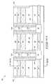
- row lines 102 , 104 , and 106extend horizontally into and out of the page and are above column lines 57 , 61 , 63 , 92 , 94 , and 96 .
- Column lines 92 , 94 , and 96also extend horizontally, but extend from left to right in FIG. 32 in a direction perpendicular to the horizontal extension of row lines 102 , 104 , and 106 .
- FIG. 32In the top view of FIG.
- row lines 102 , 104 , and 106extend horizontally and are located above the lines of material 38 illustrated in FIG. 33 .
- Column lines 57 , 61 , 63 , 92 , 94 , and 96are located underneath the lines of material 38 illustrated in FIG. 33 and extend vertically in a direction perpendicular to row lines 102 , 104 , and 106 .
- Each memory cellmay provide the functionality described above in relation to memory cell 10 of FIG. 1 .
- semiconductor material 28may be lightly doped with an n-type dopant and metal material 30 may comprise any suitable composition, and may, for example, comprise, consist essentially of, or consist of platinum, palladium, titanium nitride, aluminum, gold, or nickel.
- semiconductor material 42may be lightly doped with a p-type dopant and metal material 40 may comprise any suitable composition, and may, for example, comprise, consist essentially of, or consist of platinum silicide, aluminum, or indium.
- memory cell 68may implement the functionality of memory cell 10 of FIG. 1 (described above) as follows.
- Column lines 61 and 94may serve respectively as column lines 20 and 18 of FIG. 1
- row line 102may serve as row line 12
- memory material 32in the form of spacers 98 ) may serve as memory element 14 .
- metal material 40 and semiconductor material 42 of memory cell 68may form a Schottky diode that may serve as diode 22 of FIG. 1 with metal material 40 of memory cell 68 as a cathode of the diode and semiconductor material 42 of memory cell 68 as the anode of the diode.
- a combination of metal material 30 of memory cell 68 and semiconductor material 28 of memory cell 68may serve as diode 16 of FIG. 1 with metal material 30 functioning as an anode and semiconductor material 28 functioning as a cathode.
- a first currentmay flow from row line 102 through one of spacers 98 of memory cell 68 , metal material 40 , metal material 30 , and semiconductor material 28 to column line 94 .
- a second currentmay flow from row line 102 through the other spacer 98 of memory cell 68 , metal material 40 , metal material 30 , and semiconductor material 28 to column line 94 .
- the amount of currentmay depend on a resistive state of memory material 32 of spacers 98 and/or on a voltage applied across row line 102 and column line 94 . As was described above in relation to FIG. 1 , the current may be used, for example, to read memory cell 68 or to write a value to memory cell 68 .
- a currentmay flow from column line 61 through semiconductor material 42 , metal material 40 , spacers 98 (which comprise memory material 32 ), and spacers 100 (which may be considered part of row line 102 ) to row line 102 .
- the currentmay flow through one or both of spacers 98 of memory cell 68 .
- the Schottky diode formed by metal material 40 and semiconductor material 42may conduct a current between column line 61 and row line 102 via spacers 98 .
- spacers 90insulate spacers 98 and 100 from column line 61 to prevent a short between the column line 61 and spacers 98 and 100 .
- the amount of currentmay depend on a resistive state of memory material 32 of spacers 98 and/or on a voltage applied across row line 102 and column line 61 . As was described above in relation to FIG. 1 , the current may be used, for example, to read memory cell 68 or to write a value to memory cell 68 .
- semiconductor material 42may be lightly doped with an n-type dopant and metal material 40 may comprise any suitable composition, and may, for example, comprise, consist essentially of, or consist of platinum, palladium, titanium nitride, aluminum, gold, or nickel.
- semiconductor material 28may be lightly doped with a p-type dopant and metal material 30 may comprise any suitable composition, and may, for example, comprise, consist essentially of, or consist of platinum silicide, aluminum, or indium.
- memory cell 68may implement the functionality of memory cell 10 of FIG. 1 (described above) as follows.
- Column lines 61 and 94may serve respectively as column lines 18 and 20 of FIG. 1
- row line 102may serve as row line 12
- memory material 32in the form of spacers 98 ) may serve as memory element 14 .
- metal material 40 and semiconductor material 42 of memory cell 68may form a Schottky diode that may serve as diode 16 of FIG. 1 with metal material 40 of memory cell 68 as an anode of the diode and semiconductor material 42 as the cathode of the diode.
- a combination of metal material 30 of memory cell 68 and semiconductor material 28 of memory cell 68may serve as diode 22 of FIG. 1 with metal material 30 functioning as a cathode and semiconductor material 28 functioning as an anode.
- a first currentmay flow from column line 94 through semiconductor material 28 , metal material 30 , metal material 40 , and one of spacers 98 of memory cell 68 , to row line 102 .
- a second currentmay flow from column line 94 through semiconductor material 28 , metal material 30 , metal material 40 , and the other one of spacers 98 of memory cell 68 , to row line 102 .
- the amount of currentmay depend on a resistive state of memory material 32 of spacers 98 and/or on a voltage applied across row line 102 and column line 94 . As was described above in relation to FIG. 1 , the current may be used, for example, to read memory cell 68 or to write a value to memory cell 68 .
- a currentmay flow from row line 102 through spacers 100 , spacers 98 , metal material 40 , and semiconductor material 42 to column line 61 .
- the currentmay flow through one or both of spacers 98 of memory cell 68 .
- the amount of currentmay depend on a resistive state of memory material 32 of spacers 98 and/or on a voltage applied across row line 102 and column line 61 . As was described above in relation to FIG. 1 , the current may be used, for example, to read memory cell 68 or to write a value to memory cell 68 .
- memory cell 10Other physical embodiments of memory cell 10 are also possible.
- construction 60includes substrate 24 , and in ascending order from substrate 24 , electrically conductive material 26 , semiconductor material 42 , semiconductor material 28 , and semiconductor material 59 .
- Semiconductor material 59may comprise any suitable composition, and may, for example, comprise, consist essentially of, or consist of heavily doped silicon with either n-type dopant or p-type dopant. In some embodiments, semiconductor material 59 may be silicon having a dopant concentration of 10 19 atoms/cm 3 or higher.
- Materials 26 , 42 , 28 , and 59may be deposited over substrate 24 , for example, as illustrated in FIG. 34 .
- Construction 60may be patterned using a masking material deposited over semiconductor material 59 in order to form trenches.
- etchingis conducted to form trenches.
- the etchgoes through semiconductor material 59 , semiconductor material 28 , and semiconductor material 42 .
- the etchmay extend partially through conductive material 26 .
- the etchmay be an anisotropic etch (e.g., a dry etch) and may, in some embodiments, comprise multiple different etches.
- insulative material 36may be deposited on construction 60 and may be polished (e.g., using CMP that stops on semiconductor material 59 ) to remove portions of insulative material 36 so that semiconductor material 59 is exposed while leaving insulative material 36 intact within the etched trenches.
- FIG. 37is a diagrammatic cross-sectional view of construction 60 as observed from the same perspective as FIG. 34 .
- an electrically conductive material 44is formed over semiconductor material 59 and insulative material 36 .
- An insulative material 38is then formed over conductive material 44 .
- Construction 60may then be patterned using a masking material deposited over insulative material 38 and etched to form trenches 108 . The etch extend through insulative material 38 , conductive material 44 , and semiconductor material 59 and may go partially through semiconductor material 28 .
- the etchmay be an anisotropic etch (e.g., a dry etch) and may, in some embodiments, comprise multiple different etches.
- conductive material 44may be formed into column lines 110 , 112 , and 114 .
- column lines 110 , 112 , and 114may be electrically isolated from each other.
- insulative material 38is deposited over a top surface of construction 60 .
- the depositionmay be conformal so that insulative material 38 is in contact with sidewalls 116 and 118 and is over material 28 and the portions of insulative material 38 that were present prior to the deposition.
- An anisotropic etche.g., dry etch
- horizontally extending portions of insulative material 38have been removed and vertically extending portions of insulative material 38 remain.
- the vertically extending portions of insulative material 38may be referred to as sidewall spacers 120 .
- two of sidewall spacers 120are in contact respectively with sidewalls 116 and 118 and are laterally adjacent to sidewalls 116 and 118 .
- an anisotropic etchmay be performed that etches through semiconductor material 28 and partially through semiconductor material 42 to form trenches 123 .
- the etchmay be selective for materials 28 and 42 relative to material 38 . Consequently, trenches 123 may be self-aligned with sidewall spacers 120 since sidewall spacers 120 may determine the width of trenches 120 .
- a series of etchesmay be performed to form trenches 120 . For example, a first etch selective for material 28 may be performed followed by a second etch selective for material 42 .
- a metal material 62is deposited over the top surface of construction 60 .
- the depositionmay be conformal so that metal material 62 is in contact with sidewall spacers 120 and is in contact with material 38 and material 42 .
- Metal material 62may comprise any suitable composition, and may, for example, comprise, consist essentially of, or consist of cobalt.
- construction 60may be subjected to a process (e.g., annealing) allowing metal material 62 to react with semiconductor material 28 and semiconductor material 42 .
- a processe.g., annealing
- portions 64 of semiconductor material 28 and semiconductor material 42 in contact with metal material 62may be transformed, at least partially, into a metal silicide, for example, cobalt silicide.
- an anisotropic etchmay be performed to remove metal material 62 as well as portions of material 64 .
- the etchmay be selective for materials 62 and 64 relative to materials 38 and 42 . Consequently, the etch may be self-aligned with sidewall spacers 120 . Vertically extending portions of material 64 may remain despite the etch.
- Insulative material 36is deposited over a top surface of construction 60 .
- An etchis then performed to remove insulative material 36 to form trenches 128 .
- Trenches 128may extend from a top surface of construction 60 to a depth elevationally corresponding to a bottom surface of material 64 .
- Memory material 32is deposited over the top surface of construction 60 .
- the depositionmay be conformal so that memory material 32 is in contact with sidewall spacers 120 and material 64 and is over material 38 and material 36 .
- An anisotropic etchis then performed to form sidewall spacers. Due to the etch, horizontally extending portions of memory material 32 have been removed and vertically extending portions of memory material 32 remain.
- the vertically extending portions of memory material 32may be referred to as sidewall spacers 130 and may be in contact with sidewall spacers 120 and material 64 and laterally adjacent to sidewall spacers 120 and material 64 .
- spacers 120may be described as being laterally adjacent to sidewalls of conductive material 44 .
- conductive material 49is deposited over the top surface of construction 60 .
- the depositionmay be conformal so that conductive material 49 is in contact with sidewall spacers 130 and is over material 38 and material 36 .
- An anisotropic etchis then performed to form sidewall spacers. Due to the etch, horizontally extending portions of conductive material 49 have been removed and vertically extending portions of conductive material 49 remain.
- the vertically extending portions of conductive material 49may be referred to as sidewall spacers 132 and may be in contact with sidewall spacers 130 and laterally adjacent to sidewall spacers 120 .
- insulative material 36is deposited over a top surface of construction 60 filling trenches 128 .
- Construction 60may then be polished to remove portions of insulative material 36 that are not in trenches 128 and to give construction 60 a planar surface.
- Conductive material 49is then deposited over insulative material 38 , insulative material 36 , and spacers 120 , 130 , and 132 . Consequently, conductive material 49 may be in physical and electrical contact with spacers 132 .
- spacers 130which comprise memory material 32 , may have first portions elevationally higher than column lines 110 , 112 , and 114 and second portions elevationally lower than column lines 110 , 112 , and 114 .
- construction 60may be patterned using a masking material deposited over material 49 .
- An etche.g., an anisotropic etch
- conductive material 49may be formed into row lines 134 , 136 , and 138 .
- column lines 122 , 124 , and 126extend parallel to column lines 110 , 112 , and 114 and may be below column lines 110 , 112 , and 114 .
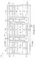
- row lines 134 , 136 , and 138extend horizontally into and out of the page and are above column lines 110 , 112 , 114 , 122 , 124 , and 126 .
- Column lines 122 , 124 , and 126also extend horizontally, but extend from left to right in FIG. 45 in a direction perpendicular to the horizontal extension of row lines 134 , 136 , and 138 .
- FIG. 45In the top view of FIG.
- row lines 134 , 136 , and 138extend horizontally and are located above the lines of material 38 illustrated in FIG. 46 .
- Column lines 110 , 112 , 114 , 122 , 124 , and 126are located underneath the lines of material 38 illustrated in FIG. 46 and extend vertically in a direction perpendicular to row lines 134 , 136 , and 138 .
- Memory cell 140may provide the functionality described above in relation to memory cell 10 of FIG. 1 .
- conductor material 26may be semiconductor material heavily doped with an n-type dopant
- semiconductor material 42may be lightly doped with a p-type dopant
- semiconductor material 59may be semiconductor material heavily doped with a p-type dopant
- semiconductor material 28may be lightly doped with an n-type dopant.
- substrate 24may be an insulative material or may be a semiconductor material lightly doped with a p-type dopant.
- memory cell 140may implement the functionality of memory cell 10 of FIG. 1 (described above) as follows.
- Column lines 112 and 124may serve respectively as column lines 20 and 18 of FIG. 1
- row line 134may serve as row line 12
- memory material 32in the form of spacers 130 ) may serve as memory element 14 .
- semiconductor materials 59 and 28 of memory cell 140may form a diode that may serve as diode 22 of FIG. 1 with semiconductor material 28 of memory cell 140 as a cathode of the diode and semiconductor material 59 as the anode of the diode.
- a combination semiconductor material 42 of memory cell 140 and conductive material 26 of memory cell 140may serve as diode 16 of FIG. 1 with semiconductor material 42 functioning as an anode and semiconductor material 26 functioning as a cathode.
- a first currentmay flow from row line 134 through one of spacers 130 of memory cell 140 , material 64 , and semiconductor material 42 to column line 124 (which comprises conductive material 26 ).
- a second currentmay flow from row line 134 through the other spacer 130 of memory cell 140 , material 64 , and semiconductor material 42 to column line 124 .
- material 64may act as an electrode between the diode formed from semiconductor material 59 and semiconductor material 28 and the diode formed from semiconductor material 42 and conductor material 26 .
- first portions of spacers 130 laterally adjacent to material 64may conduct current while second portions of spacers 130 laterally adjacent to spacers 120 might not conduct current or might conduct a negligible amount of current since the second portions are not laterally adjacent or in physical contact with material 64 .
- the amount of currentmay depend on a resistive state of memory material 32 of spacers 130 and/or on a voltage applied across row line 134 and column line 124 . As was described above in relation to FIG. 1 , the current may be used, for example, to read memory cell 140 or to write a value to memory cell 140 .
- a currentmay flow from column line 112 through semiconductor material 59 , semiconductor material 28 , material 64 , spacers 130 (which comprise memory material 32 ), and spacers 132 (which may be considered part of row line 134 ) to row line 134 .
- the currentmay flow through one or both of spacers 130 of memory cell 140 .
- spacers 120insulate spacers 130 and 132 from column line 112 to prevent a short between the column line 112 and spacers 130 and 132 .
- the amount of currentmay depend on a resistive state of memory material 32 of spacers 130 and/or on a voltage applied across row line 134 and column line 112 . As was described above in relation to FIG. 1 , the current may be used, for example, to read memory cell 140 or to write a value to memory cell 140 .
- conductor material 26may be semiconductor material heavily doped with a p-type dopant
- semiconductor material 42may be lightly doped with an n-type dopant
- semiconductor material 59may be semiconductor material heavily doped with an n-type dopant
- semiconductor material 28may be lightly doped with a p-type dopant.
- substrate 24may be an insulative material or may be a semiconductor material lightly doped with an n-type dopant.
- memory cell 140may implement the functionality of memory cell 10 of FIG. 1 (described above) as follows.
- Column lines 112 and 124may serve respectively as column lines 18 and 20 of FIG. 1
- row line 134may serve as row line 12
- memory material 32in the form of spacers 130 ) may serve as memory element 14 .
- semiconductor materials 59 and 28 of memory cell 140may form a diode that may serve as diode 16 of FIG. 1 with semiconductor material 28 of memory cell 140 as an anode of the diode and semiconductor material 59 as a cathode of the diode.
- a combination semiconductor material 42 of memory cell 140 and conductive material 26 of memory cell 140may serve as diode 22 of FIG. 1 with semiconductor material 42 functioning as a cathode and semiconductor material 26 functioning as an anode.
- a first currentmay flow from column line 124 through semiconductor material 42 , material 64 , one of spacers 130 of memory cell 140 , and one of spacers 132 of memory cell 140 to row line 134 .
- a second currentmay flow from column line 124 through semiconductor material 42 , material 64 , the other one of spacers 130 , and the other one of spacers 132 to row line 134 .
- the amount of currentmay depend on a resistive state of memory material 32 of spacers 130 and/or on a voltage applied across row line 134 and column line 124 . As was described above in relation to FIG. 1 , the current may be used, for example, to read memory cell 140 or to write a value to memory cell 140 .
- a currentmay flow from row line 134 through spacers 132 , spacers 130 , material 64 , semiconductor material 28 , and semiconductor material 59 to column line 112 .
- the currentmay flow through one or both of spacers 130 of memory cell 140 .
- the amount of currentmay depend on a resistive state of memory material 32 of spacers 130 and/or on a voltage applied across row line 134 and column line 112 . As was described above in relation to FIG. 1 , the current may be used, for example, to read memory cell 140 or to write a value to memory cell 140 .
- a memory device constructioncomprises a first column line extending parallel to a second column line, the first column line being above the second column line; a row line above the second column line and extending perpendicular to the first column line and the second column line; memory material disposed to be selectively and reversibly configured in one of two or more different resistive states; a first diode configured to conduct a first current between the first column line and the row line via the memory material; and a second diode configured to conduct a second current between the second column line and the row line via the memory material.
- the row linemay be below the first column lines.
- the first diodemay be a Schottky diode comprising a semiconductor anode and a metal cathode and the second diode may be a Schottky diode comprising a metal anode and a semiconductor cathode.
- the metal cathodemay extend vertically so that a first portion of the metal cathode is elevationally higher than the row line and a second portion of the metal cathode is elevationally lower than the row line.
- a memory device constructioncomprises a first horizontally extending conductive line; a second conductive line extending perpendicular to the first conductive line; a diode; a first vertically extending deposit of memory material laterally adjacent to a first sidewall of the second conductive line, the memory material being disposed to be selectively and reversibly configured in one of two or more different resistive states; a second vertically extending deposit of the memory material laterally adjacent to a second sidewall of the second conductive line, the second sidewall opposing the first sidewall; and wherein when the memory device is configured to simultaneously conduct a first current between the second conductive line and the first conductive line via the diode and the first deposit and to conduct a second current between the second conductive line and the first conductive line via the diode and the second deposit.
- a memory cell forming methodcomprises providing a substrate; forming, over the substrate, a horizontally extending memory material disposed to be selectively and reversibly configured in one of two or more different resistive states; forming a row line over the memory material; forming a vertically extending insulative material laterally adjacent to the memory material and the row line; forming a first portion of a diode laterally adjacent to the insulative material, the first portion extending vertically to a position elevationally higher than the memory material and the row line; forming a second portion of the diode extending horizontally above the first portion of the diode, the second portion being in direct physical contact with the first portion; forming a horizontally extending column line over the second portion of the diode; and wherein the memory cell is configured to conduct a current between the column line and the row line via the diode and the memory material.
- a memory cell forming methodcomprises providing a substrate; forming a first portion of a diode above the substrate; forming a second portion of the diode above the first portion of the diode; forming a horizontally extending column line over the second portion of the diode; forming a vertically extending insulative material laterally adjacent to the column line and the second portion of the diode; forming a vertically extending memory material laterally adjacent to the insulative material and in contact with the first portion of the diode, the memory material being disposed to be selectively and reversibly configured in one of two or more different resistive states; forming a vertically extending conductive material laterally adjacent to the memory material and in contact with the memory material; forming a horizontally extending row line over the column line and the vertically extending conductive material and in contact with the vertically extending conductive material; and wherein the memory cell is configured to conduct a current between the column line and the row line via the diode and the memory material
- a semiconductor construction forming methodcomprises providing a substrate; forming a first semiconductor material over the substrate, a second semiconductor material over the first semiconductor material, a third semiconductor material over the second semiconductor material, and a fourth semiconductor material over the third semiconductor material wherein the first and second semiconductor materials comprise different dopants relative to one another and the third and fourth semiconductor materials comprise different dopants relative to one another; etching a first trench extending entirely through the fourth semiconductor material and partially through the third semiconductor material; depositing an insulative material on a sidewall of the trench, the insulative material being in contact with the first semiconductor material and the second semiconductor material; etching a second trench extending from a bottom surface of the first trench entirely through the third semiconductor material and partially through the second semiconductor material; depositing a metal on a sidewall of the second trench, the metal being in contact with the insulative material, the third semiconductor material, and the second semiconductor material; reacting the metal with the third semiconductor material and the second semiconductor material so that a first portion of the third semiconductor material and a second portion of
Landscapes
- Engineering & Computer Science (AREA)
- Manufacturing & Machinery (AREA)
- Semiconductor Memories (AREA)
Abstract
Description
Claims (27)
Priority Applications (4)
| Application Number | Priority Date | Filing Date | Title |
|---|---|---|---|
| US12/141,388US8134137B2 (en) | 2008-06-18 | 2008-06-18 | Memory device constructions, memory cell forming methods, and semiconductor construction forming methods |
| US13/418,082US9111788B2 (en) | 2008-06-18 | 2012-03-12 | Memory device constructions, memory cell forming methods, and semiconductor construction forming methods |
| US14/680,431US9257430B2 (en) | 2008-06-18 | 2015-04-07 | Semiconductor construction forming methods |
| US15/003,606US9559301B2 (en) | 2008-06-18 | 2016-01-21 | Methods of forming memory device constructions, methods of forming memory cells, and methods of forming semiconductor constructions |
Applications Claiming Priority (1)
| Application Number | Priority Date | Filing Date | Title |
|---|---|---|---|
| US12/141,388US8134137B2 (en) | 2008-06-18 | 2008-06-18 | Memory device constructions, memory cell forming methods, and semiconductor construction forming methods |
Related Child Applications (1)
| Application Number | Title | Priority Date | Filing Date |
|---|---|---|---|
| US13/418,082DivisionUS9111788B2 (en) | 2008-06-18 | 2012-03-12 | Memory device constructions, memory cell forming methods, and semiconductor construction forming methods |
Publications (2)
| Publication Number | Publication Date |
|---|---|
| US20090316467A1 US20090316467A1 (en) | 2009-12-24 |
| US8134137B2true US8134137B2 (en) | 2012-03-13 |
Family
ID=41431119
Family Applications (4)
| Application Number | Title | Priority Date | Filing Date |
|---|---|---|---|
| US12/141,388Active2030-02-17US8134137B2 (en) | 2008-06-18 | 2008-06-18 | Memory device constructions, memory cell forming methods, and semiconductor construction forming methods |
| US13/418,082ActiveUS9111788B2 (en) | 2008-06-18 | 2012-03-12 | Memory device constructions, memory cell forming methods, and semiconductor construction forming methods |
| US14/680,431ActiveUS9257430B2 (en) | 2008-06-18 | 2015-04-07 | Semiconductor construction forming methods |
| US15/003,606ActiveUS9559301B2 (en) | 2008-06-18 | 2016-01-21 | Methods of forming memory device constructions, methods of forming memory cells, and methods of forming semiconductor constructions |
Family Applications After (3)
| Application Number | Title | Priority Date | Filing Date |
|---|---|---|---|
| US13/418,082ActiveUS9111788B2 (en) | 2008-06-18 | 2012-03-12 | Memory device constructions, memory cell forming methods, and semiconductor construction forming methods |
| US14/680,431ActiveUS9257430B2 (en) | 2008-06-18 | 2015-04-07 | Semiconductor construction forming methods |
| US15/003,606ActiveUS9559301B2 (en) | 2008-06-18 | 2016-01-21 | Methods of forming memory device constructions, methods of forming memory cells, and methods of forming semiconductor constructions |
Country Status (1)
| Country | Link |
|---|---|
| US (4) | US8134137B2 (en) |
Cited By (1)
| Publication number | Priority date | Publication date | Assignee | Title |
|---|---|---|---|---|
| US20150171324A1 (en)* | 2012-01-19 | 2015-06-18 | Panasonic Corporation | Method of manufacturing variable resistance nonvolatile memory device, and variable resistance nonvolatile memory device |
Families Citing this family (24)
| Publication number | Priority date | Publication date | Assignee | Title |
|---|---|---|---|---|
| US7768812B2 (en) | 2008-01-15 | 2010-08-03 | Micron Technology, Inc. | Memory cells, memory cell programming methods, memory cell reading methods, memory cell operating methods, and memory devices |
| JP2009252830A (en)* | 2008-04-02 | 2009-10-29 | Toshiba Corp | Method of manufacturing semiconductor device |
| US8034655B2 (en) | 2008-04-08 | 2011-10-11 | Micron Technology, Inc. | Non-volatile resistive oxide memory cells, non-volatile resistive oxide memory arrays, and methods of forming non-volatile resistive oxide memory cells and memory arrays |
| US8211743B2 (en) | 2008-05-02 | 2012-07-03 | Micron Technology, Inc. | Methods of forming non-volatile memory cells having multi-resistive state material between conductive electrodes |
| US8134137B2 (en) | 2008-06-18 | 2012-03-13 | Micron Technology, Inc. | Memory device constructions, memory cell forming methods, and semiconductor construction forming methods |
| US9343665B2 (en) | 2008-07-02 | 2016-05-17 | Micron Technology, Inc. | Methods of forming a non-volatile resistive oxide memory cell and methods of forming a non-volatile resistive oxide memory array |
| US8431492B2 (en) | 2010-02-02 | 2013-04-30 | Sandisk 3D Llc | Memory cell that includes a sidewall collar for pillar isolation and methods of forming the same |
| US8686419B2 (en)* | 2010-02-23 | 2014-04-01 | Sandisk 3D Llc | Structure and fabrication method for resistance-change memory cell in 3-D memory |
| US8411477B2 (en) | 2010-04-22 | 2013-04-02 | Micron Technology, Inc. | Arrays of vertically stacked tiers of non-volatile cross point memory cells, methods of forming arrays of vertically stacked tiers of non-volatile cross point memory cells, and methods of reading a data value stored by an array of vertically stacked tiers of non-volatile cross point memory cells |
| US8427859B2 (en) | 2010-04-22 | 2013-04-23 | Micron Technology, Inc. | Arrays of vertically stacked tiers of non-volatile cross point memory cells, methods of forming arrays of vertically stacked tiers of non-volatile cross point memory cells, and methods of reading a data value stored by an array of vertically stacked tiers of non-volatile cross point memory cells |
| US8289763B2 (en) | 2010-06-07 | 2012-10-16 | Micron Technology, Inc. | Memory arrays |
| US8351242B2 (en) | 2010-09-29 | 2013-01-08 | Micron Technology, Inc. | Electronic devices, memory devices and memory arrays |
| US8759809B2 (en) | 2010-10-21 | 2014-06-24 | Micron Technology, Inc. | Integrated circuitry comprising nonvolatile memory cells having platelike electrode and ion conductive material layer |
| US8796661B2 (en) | 2010-11-01 | 2014-08-05 | Micron Technology, Inc. | Nonvolatile memory cells and methods of forming nonvolatile memory cell |
| US8526213B2 (en) | 2010-11-01 | 2013-09-03 | Micron Technology, Inc. | Memory cells, methods of programming memory cells, and methods of forming memory cells |
| US9454997B2 (en) | 2010-12-02 | 2016-09-27 | Micron Technology, Inc. | Array of nonvolatile memory cells having at least five memory cells per unit cell, having a plurality of the unit cells which individually comprise three elevational regions of programmable material, and/or having a continuous volume having a combination of a plurality of vertically oriented memory cells and a plurality of horizontally oriented memory cells; array of vertically stacked tiers of nonvolatile memory cells |
| US8431458B2 (en) | 2010-12-27 | 2013-04-30 | Micron Technology, Inc. | Methods of forming a nonvolatile memory cell and methods of forming an array of nonvolatile memory cells |
| US8791447B2 (en) | 2011-01-20 | 2014-07-29 | Micron Technology, Inc. | Arrays of nonvolatile memory cells and methods of forming arrays of nonvolatile memory cells |
| US8488365B2 (en) | 2011-02-24 | 2013-07-16 | Micron Technology, Inc. | Memory cells |
| US8537592B2 (en) | 2011-04-15 | 2013-09-17 | Micron Technology, Inc. | Arrays of nonvolatile memory cells and methods of forming arrays of nonvolatile memory cells |
| CN107579087B (en)* | 2016-07-04 | 2020-04-07 | 中芯国际集成电路制造(上海)有限公司 | Memory cell array structure and electronic device |
| CN108630722B (en)* | 2017-03-22 | 2020-10-30 | 中芯国际集成电路制造(上海)有限公司 | Memory cell and method of forming the same, memory array structure and method of forming the same |
| TWI758077B (en)* | 2021-01-21 | 2022-03-11 | 凌北卿 | Non-volatile memory device having pn diode |
| TWI838615B (en)* | 2021-03-22 | 2024-04-11 | 凌北卿 | Non-volatile memory device having schottky diode |
Citations (142)
| Publication number | Priority date | Publication date | Assignee | Title |
|---|---|---|---|---|
| US4715685A (en) | 1985-03-04 | 1987-12-29 | Energy Conversion Devices, Inc. | Liquid crystal display having potential source in a diode ring |
| US4964080A (en) | 1990-03-09 | 1990-10-16 | Intel Corporation | Three-dimensional memory cell with integral select transistor |
| US5049970A (en) | 1987-11-17 | 1991-09-17 | Sharp Kabushiki Kaisha | High resistive element |
| US5122476A (en) | 1991-01-28 | 1992-06-16 | Micron Technology, Inc. | Double DRAM cell |
| US20020018355A1 (en) | 1998-11-16 | 2002-02-14 | Johnson Mark G. | Vertically stacked field programmable nonvolatile memory and method of fabrication |
| US20020196695A1 (en) | 2001-05-30 | 2002-12-26 | Stmicroelectronics S.R.L. | Column multiplexer for semiconductor memories |
| US6524867B2 (en) | 2000-12-28 | 2003-02-25 | Micron Technology, Inc. | Method for forming platinum-rhodium stack as an oxygen barrier |
| US20030218929A1 (en) | 2002-05-24 | 2003-11-27 | Heiko Fibranz | Circuit configuration having a flow controller, integrated memory device, and test configuration having such a circuit configuration |
| US20030223283A1 (en) | 2002-04-03 | 2003-12-04 | Mitsubishi Denki Kabushiki Kaisha | Magnetic memory device |
| US20040002186A1 (en)* | 2002-06-27 | 2004-01-01 | Vyvoda Michael A. | Electrically isolated pillars in active devices |
| US6693821B2 (en) | 2001-06-28 | 2004-02-17 | Sharp Laboratories Of America, Inc. | Low cross-talk electrically programmable resistance cross point memory |
| US20040100835A1 (en) | 2002-11-27 | 2004-05-27 | Nec Corporation | Magnetic memory cell and magnetic random access memory using the same |
| US20040108528A1 (en) | 2001-06-28 | 2004-06-10 | Sharp Laboratories Of America, Inc. | Cross-point resistor memory array and method of fabrication |
| US6753561B1 (en)* | 2002-08-02 | 2004-06-22 | Unity Semiconductor Corporation | Cross point memory array using multiple thin films |
| US6753562B1 (en) | 2003-03-27 | 2004-06-22 | Sharp Laboratories Of America, Inc. | Spin transistor magnetic random access memory device |
| US20040124407A1 (en) | 2000-02-11 | 2004-07-01 | Kozicki Michael N. | Scalable programmable structure, an array including the structure, and methods of forming the same |
| US6778421B2 (en) | 2002-03-14 | 2004-08-17 | Hewlett-Packard Development Company, Lp. | Memory device array having a pair of magnetic bits sharing a common conductor line |
| US6785159B2 (en) | 2002-08-29 | 2004-08-31 | Micron Technology, Inc. | Combination etch stop and in situ resistor in a magnetoresistive memory and methods for fabricating same |
| US6806531B1 (en) | 2003-04-07 | 2004-10-19 | Silicon Storage Technology, Inc. | Non-volatile floating gate memory cell with floating gates formed in cavities, and array thereof, and method of formation |
| US20040245547A1 (en) | 2003-06-03 | 2004-12-09 | Hitachi Global Storage Technologies B.V. | Ultra low-cost solid-state memory |
| US6834008B2 (en) | 2002-08-02 | 2004-12-21 | Unity Semiconductor Corporation | Cross point memory array using multiple modes of operation |
| US20050032100A1 (en) | 2003-06-24 | 2005-02-10 | California Institute Of Technology | Electrochemical method and resulting structures for attaching molecular and biomolecular structures to semiconductor micro and nanostructures |
| US20050054119A1 (en) | 2003-09-05 | 2005-03-10 | Sharp Laboratories Of America, Inc. | Buffered-layer memory cell |
| JP2005175457A (en) | 2003-12-08 | 2005-06-30 | Sharp Corp | RRAM memory cell electrode |
| US20050161747A1 (en) | 2004-01-26 | 2005-07-28 | Hsiang-Lan Lung | Thin film phase-change memory |
| US6930324B2 (en) | 2002-12-31 | 2005-08-16 | Infineon Technologies Ag | Device architecture and process for improved vertical memory arrays |
| US6940113B2 (en) | 2001-06-28 | 2005-09-06 | Sharp Laboratories Of America, Inc. | Trench isolated cross-point memory array |
| US6946702B2 (en) | 2003-06-03 | 2005-09-20 | Winbond Electronics Corp. | Resistance random access memory |
| US20050205943A1 (en) | 2004-03-17 | 2005-09-22 | Sanyo Electric Co., Ltd. | Memory and method of fabricating the same |
| US6955992B2 (en) | 2003-09-30 | 2005-10-18 | Sharp Laboratories Of America, Inc. | One mask PT/PCMO/PT stack etching process for RRAM applications |
| US6958273B2 (en) | 2003-03-21 | 2005-10-25 | Silicon Storage Technology, Inc. | Self-aligned method of forming a semiconductor memory array of floating gate memory cells with buried floating gate, pointed floating gate and pointed channel region, and a memory array made thereby |
| US6961258B2 (en) | 2001-06-30 | 2005-11-01 | Ovonyx, Inc. | Pore structure for programmable device |
| US20050250281A1 (en) | 2004-04-26 | 2005-11-10 | Infineon Technologies Ag | Method for manufacturing resistively switching memory devices |
| US6970375B2 (en) | 2002-08-02 | 2005-11-29 | Unity Semiconductor Corporation | Providing a reference voltage to a cross point memory array |
| US20050287741A1 (en) | 2004-06-28 | 2005-12-29 | Yi Ding | Nonvolatile memory fabrication methods in which a dielectric layer underlying a floating gate layer is spaced from an edge of an isolation trench and/or an edge of the floating gate layer |
| WO2006003620A1 (en) | 2004-06-30 | 2006-01-12 | Koninklijke Philips Electronics N.V. | Method for manufacturing an electric device with a layer of conductive material contacted by nanowire |
| JP2006040981A (en) | 2004-07-22 | 2006-02-09 | Sharp Corp | High density SOI crosspoint memory array and method for manufacturing the same |
| US20060035451A1 (en) | 2003-05-20 | 2006-02-16 | Sharp Laboratories Of America, Inc. | High-density SOI cross-point memory fabricating method |
| US7002197B2 (en) | 2004-01-23 | 2006-02-21 | Hewlett-Packard Development Company, L.P. | Cross point resistive memory array |
| US7005350B2 (en) | 2002-12-31 | 2006-02-28 | Matrix Semiconductor, Inc. | Method for fabricating programmable memory array structures incorporating series-connected transistor strings |
| US7009278B2 (en) | 2003-11-24 | 2006-03-07 | Sharp Laboratories Of America, Inc. | 3d rram |
| US20060062049A1 (en) | 2004-09-17 | 2006-03-23 | Seok-Heon Lee | Methods for programming user data and confirmation information in nonvolatile memory devices |
| US7029925B2 (en) | 2002-01-31 | 2006-04-18 | Texas Instruments Incorporated | FeRAM capacitor stack etch |
| JP2006121044A (en) | 2004-10-21 | 2006-05-11 | Sharp Corp | Chemical mechanical polishing of PCMO thin film in RRAM equipment |
| US7050316B1 (en) | 2004-03-09 | 2006-05-23 | Silicon Storage Technology, Inc. | Differential non-volatile content addressable memory cell and array using phase changing resistor storage elements |
| US7067862B2 (en) | 2002-08-02 | 2006-06-27 | Unity Semiconductor Corporation | Conductive memory device with conductive oxide electrodes |
| US20060160304A1 (en) | 2005-01-19 | 2006-07-20 | Sharp Laboratories Of America, Inc. | Non-volatile memory resistor cell with nanotip electrode |
| US20060170027A1 (en) | 2005-01-31 | 2006-08-03 | Samsung Electronics Co., Ltd. | Nonvolatile memory device made of resistance material and method of fabricating the same |
| US20060171200A1 (en) | 2004-02-06 | 2006-08-03 | Unity Semiconductor Corporation | Memory using mixed valence conductive oxides |
| US7148011B2 (en) | 2000-09-25 | 2006-12-12 | Japan As Represented By General Director Of Agency Of National Center For Child Health And Development | Method of testing for allergic diseases |
| US20060284242A1 (en) | 2005-06-07 | 2006-12-21 | Jo Sang-Youn | Non-volatile memory device having floating gate and methods forming the same |
| US20070010082A1 (en) | 2005-07-05 | 2007-01-11 | Cay-Uwe Pinnow | Structure and method for manufacturing phase change memories with particular switching characteristics |
| US20070015330A1 (en) | 2005-07-18 | 2007-01-18 | Sharp Laboratories Of America, Inc. | Metal/semiconductor/metal (MSM) back-to-back Schottky diode |
| US7180801B2 (en) | 2000-12-08 | 2007-02-20 | Stmicroelectronics S.A. | Memory circuit with shared redundancy |
| US7180160B2 (en) | 2004-07-30 | 2007-02-20 | Infineon Technologies Ag | MRAM storage device |
| US20070045615A1 (en) | 2005-08-31 | 2007-03-01 | Samsung Electronics Co., Ltd. | Non-volatile organic resistance random access memory device and method of manufacturing the same |
| US20070048990A1 (en) | 2005-08-30 | 2007-03-01 | Sharp Laboratories Of America, Inc. | Method of buffer layer formation for RRAM thin film deposition |
| US7187201B1 (en) | 2004-06-24 | 2007-03-06 | Xilinx, Inc. | Programmable logic device suitable for implementation in molecular electronics |
| US7193267B2 (en) | 2001-06-28 | 2007-03-20 | Sharp Laboratories Of America, Inc. | Cross-point resistor memory array |
| US20070109835A1 (en) | 2005-11-17 | 2007-05-17 | Sharp Laboratories Of America, Inc. | Cross-point RRAM memory array having low bit line crosstalk |
| US20070121369A1 (en) | 2004-05-27 | 2007-05-31 | Thomas Happ | Resistive memory cell arrangement and a semiconductor memory including the same |
| US20070132049A1 (en) | 2005-12-12 | 2007-06-14 | Stipe Barry C | Unipolar resistance random access memory (RRAM) device and vertically stacked architecture |
| US7233024B2 (en) | 2003-03-31 | 2007-06-19 | Sandisk 3D Llc | Three-dimensional memory device incorporating segmented bit line memory array |
| US20070165434A1 (en) | 2006-01-19 | 2007-07-19 | Samsung Electronics Co., Ltd. | Resistive RAM having at least one varistor and methods of operating the same |
| US7247876B2 (en)* | 2000-06-30 | 2007-07-24 | Intel Corporation | Three dimensional programmable device and method for fabricating the same |
| CN101005113A (en) | 2005-12-27 | 2007-07-25 | 旺宏电子股份有限公司 | Method for forming self-aligned thermally isolated cells in variable resistance memory arrays |
| US20070173019A1 (en) | 2006-01-09 | 2007-07-26 | Macronix International Co., Ltd. | Programmable Resistive Ram and Manufacturing Method |
| US7273791B2 (en) | 2000-11-09 | 2007-09-25 | Micron Technology, Inc. | Methods for forming a conductive structure using oxygen diffusion through one metal layer to oxidize a second metal layer |
| US20070224770A1 (en) | 2006-03-25 | 2007-09-27 | Makoto Nagashima | Systems and methods for fabricating self-aligned memory cell |
| US20070231988A1 (en) | 2006-03-09 | 2007-10-04 | Samsung Electronics Co., Ltd. | Method of fabricating nanowire memory device and system of controlling nanowire formation used in the same |
| CN101051670A (en) | 2007-04-19 | 2007-10-10 | 复旦大学 | Preparing method for RRAM to avoid forming phenomenon using CuxO as storage medium |
| US20070246795A1 (en) | 2006-04-20 | 2007-10-25 | Micron Technology, Inc. | Dual depth shallow trench isolation and methods to form same |
| US20070257257A1 (en) | 2006-02-20 | 2007-11-08 | Samsung Electronics Co., Ltd. | Nonvolatile memory device including amorphous alloy metal oxide layer and method of manufacturing the same |
| US20070268739A1 (en) | 2006-03-08 | 2007-11-22 | Samsung Electronics Co., Ltd. | Nanowire memory device and method of manufacturing the same |
| KR20070111840A (en) | 2006-05-19 | 2007-11-22 | 삼성전자주식회사 | Nonvolatile Memory Device Using Oxygen-deficient Metal Oxide and Manufacturing Method Thereof |
| US20070268742A1 (en) | 2006-05-18 | 2007-11-22 | Micron Technology, Inc. | Memory Architecture and Cell Design Employing Two Access Transistors |
| US20070285965A1 (en) | 2007-06-11 | 2007-12-13 | Kabushiki Kaisha Toshiba | Resistance change memory device |
| KR20070118865A (en) | 2006-06-13 | 2007-12-18 | 광주과학기술원 | Non-volatile Memory, Manufacturing Method and Device Thereof |
| US20070295950A1 (en) | 2006-06-27 | 2007-12-27 | Samsung Electronics Co., Ltd. | Variable resistance random access memory device and a method of fabricating the same |
| US20080014750A1 (en) | 2006-07-14 | 2008-01-17 | Makoto Nagashima | Systems and methods for fabricating self-aligned memory cell |
| US20080012064A1 (en) | 2006-04-21 | 2008-01-17 | Samsung Electronics Co., Ltd. | Nonvolatile memory device and methods of operating and fabricating the same |
| US7323349B2 (en) | 2005-05-02 | 2008-01-29 | Sharp Laboratories Of America, Inc. | Self-aligned cross point resistor memory array |
| US20080026547A1 (en) | 2006-07-27 | 2008-01-31 | Samsung Electronics Co. Ltd. | Method of forming poly-si pattern, diode having poly-si pattern, multi-layer cross point resistive memory device having poly-si pattern, and method of manufacturing the diode and the memory device |
| US20080029842A1 (en) | 2006-08-02 | 2008-02-07 | Ralf Symanczyk | CBRAM cell and CBRAM array, and method of operating thereof |
| US20080029754A1 (en) | 2006-08-01 | 2008-02-07 | Samsung Electronics Co., Ltd. | Variable resistance non-volatile memory devices including a uniformly narrow contact layer and methods of manufacturing same |
| US20080048165A1 (en) | 2006-07-24 | 2008-02-28 | Seiko Epson Corporation | Variable resistance element and resistance variable type memory device |
| US20080049487A1 (en) | 2006-08-22 | 2008-02-28 | Sharp Kabushiki Kaisha | Semiconductor memory device |
| US20080073635A1 (en) | 2006-09-21 | 2008-03-27 | Masahiro Kiyotoshi | Semiconductor Memory and Method of Manufacturing the Same |
| US20080080229A1 (en) | 2006-10-02 | 2008-04-03 | Byung-Gil Choi | Variable resistive memory wordline switch |
| US20080102278A1 (en) | 2006-10-27 | 2008-05-01 | Franz Kreupl | Carbon filament memory and method for fabrication |
| US7388775B2 (en) | 2005-03-30 | 2008-06-17 | Ovonyx, Inc. | Detecting switching of access elements of phase change memory cells |
| US7393785B2 (en) | 1998-08-26 | 2008-07-01 | Micron Technology, Inc. | Methods and apparatus for forming rhodium-containing layers |
| US20080157257A1 (en) | 2005-05-09 | 2008-07-03 | Nantero, Inc. | Nonvolatile nanotube diodes and nonvolatile nanotube blocks and systems using same and methods of making same |
| US20080175031A1 (en) | 2007-01-23 | 2008-07-24 | Samsung Electronics Co., Ltd. | Memory cell of a resistive semiconductor memory device, a resistive semiconductor memory device having a three-dimensional stack structure, and related methods |
| US7405967B2 (en) | 1998-12-04 | 2008-07-29 | Axon Technologies Corporation | Microelectronic programmable device and methods of forming and programming the same |
| US20080185571A1 (en) | 2007-02-01 | 2008-08-07 | Thomas Happ | Resistive memory including buried word lines |
| US20080232160A1 (en) | 2007-02-27 | 2008-09-25 | International Business Machines Corporation | Rectifying element for a crosspoint based memory array architecture |
| US20080247219A1 (en) | 2007-04-04 | 2008-10-09 | Samsung Electronics Co., Ltd. | Resistive Random Access Memory Devices Including Sidewall Resistive Layers and Related Methods |
| US20080259672A1 (en) | 2007-04-17 | 2008-10-23 | Macronix International Co., Ltd. | 4f2 self align side wall active phase change memory |
| US20080258126A1 (en) | 2007-04-17 | 2008-10-23 | Macronix International Co., Ltd. | Memory Cell Sidewall Contacting Side Electrode |
| US20080303014A1 (en) | 2005-12-20 | 2008-12-11 | Nxp B.V. | Vertical Phase Change Memory Cell and Methods For Manufacturing Thereof |
| US20090014706A1 (en) | 2007-07-13 | 2009-01-15 | Macronix International Co., Ltd. | 4f2 self align fin bottom electrodes fet drive phase change memory |
| US20090014707A1 (en) | 2006-10-20 | 2009-01-15 | Wei Lu | Non-volatile solid state resistive switching devices |
| US20090085121A1 (en) | 2007-09-28 | 2009-04-02 | Human Park | Condensed Memory Cell Structure Using a FinFET |
| US7544987B2 (en) | 2000-08-30 | 2009-06-09 | Micron Technology, Inc. | High-k dielectric materials and processes for manufacturing them |
| US7557424B2 (en)* | 2007-01-03 | 2009-07-07 | International Business Machines Corporation | Reversible electric fuse and antifuse structures for semiconductor devices |
| US7560815B1 (en) | 1998-08-27 | 2009-07-14 | Micron Technology, Inc. | Device structures including ruthenium silicide diffusion barrier layers |
| US20090180309A1 (en) | 2008-01-15 | 2009-07-16 | Jun Liu | Memory Cells, Memory Cell Programming Methods, Memory Cell Reading Methods, Memory Cell Operating Methods, and Memory Devices |
| US7570511B2 (en) | 2006-11-10 | 2009-08-04 | Samsung Electronics Co., Ltd. | Semiconductor memory device having a three-dimensional cell array structure |
| US20090250681A1 (en) | 2008-04-08 | 2009-10-08 | John Smythe | Non-Volatile Resistive Oxide Memory Cells, Non-Volatile Resistive Oxide Memory Arrays, And Methods Of Forming Non-Volatile Resistive Oxide Memory Cells And Memory Arrays |
| WO2009127187A2 (en) | 2008-04-15 | 2009-10-22 | Technische Universität Dresden | Apparatus and method for producing switchable temporary magnetism in oxidic materials by means of electrical fields |
| US20090268532A1 (en) | 2008-04-28 | 2009-10-29 | Qimonda Ag | Systems and Methods for Writing to a Memory |
| US20090267047A1 (en) | 2008-04-28 | 2009-10-29 | Hitachi, Ltd. | Semiconductor memory device and manufacturing method thereof |
| US20090272960A1 (en) | 2008-05-02 | 2009-11-05 | Bhaskar Srinivasan | Non-Volatile Resistive Oxide Memory Cells, and Methods Of Forming Non-Volatile Resistive Oxide Memory Cells |
| US20090303780A1 (en) | 2008-06-09 | 2009-12-10 | Qimonda Ag | Integrated circuit including an array of diodes coupled to a layer of resistance changing material |
| US20090317540A1 (en) | 2008-06-18 | 2009-12-24 | Gurtej Sandhu | Methods Of Forming A Non-Volatile Resistive Oxide Memory Array |
| US20090316467A1 (en) | 2008-06-18 | 2009-12-24 | Jun Liu | Memory Device Constructions, Memory Cell Forming Methods, and Semiconductor Construction Forming Methods |
| US20090315090A1 (en) | 2008-06-23 | 2009-12-24 | Rolf Weis | Isolation Trenches with Conductive Plates |
| US7639523B2 (en) | 2006-11-08 | 2009-12-29 | Symetrix Corporation | Stabilized resistive switching memory |
| US20100003782A1 (en) | 2008-07-02 | 2010-01-07 | Nishant Sinha | Methods Of Forming A Non-Volatile Resistive Oxide Memory Cell And Methods Of Forming A Non-Volatile Resistive Oxide Memory Array |
| US7679812B2 (en) | 2005-07-22 | 2010-03-16 | Qualcomm Mems Technologies Inc. | Support structure for MEMS device and methods therefor |
| US20100065836A1 (en) | 2008-09-18 | 2010-03-18 | Hynix Semiconductor Inc. | Resistive memory device and method of fabricating the same |
| US7687793B2 (en)* | 2001-05-11 | 2010-03-30 | Micron Technology, Inc. | Resistance variable memory cells |
| US7696077B2 (en) | 2006-07-14 | 2010-04-13 | Micron Technology, Inc. | Bottom electrode contacts for semiconductor devices and methods of forming same |
| US20100110759A1 (en) | 2008-11-03 | 2010-05-06 | Seagate Technology Llc | Programmable resistive memory cell with filament placement structure |
| US7727908B2 (en) | 2006-08-03 | 2010-06-01 | Micron Technology, Inc. | Deposition of ZrA1ON films |
| US20100135061A1 (en) | 2008-12-02 | 2010-06-03 | Shaoping Li | Non-Volatile Memory Cell with Ferroelectric Layer Configurations |
| WO2010068221A1 (en) | 2008-12-12 | 2010-06-17 | Hewlett-Packard Development Company, L.P. | Memristive device |
| US20100163829A1 (en) | 2008-12-30 | 2010-07-01 | Industrial Technology Research Institute | Conductive bridging random access memory device and method of manufacturing the same |
| US20100163820A1 (en) | 2008-12-26 | 2010-07-01 | Min Seok Son | Phase change memory device having a reduced contact area and method for manufacturing the same |
| US7751163B2 (en) | 2006-09-29 | 2010-07-06 | Qimonda Ag | Electric device protection circuit and method for protecting an electric device |
| WO2010082928A1 (en) | 2009-01-15 | 2010-07-22 | Hewlett-Packard Development Company, L.P. | Silicon-based memristive device |
| WO2010085241A1 (en) | 2009-01-20 | 2010-07-29 | Hewlett-Packard Development Company, L.P. | Multilayer memristive devices |
| WO2010087854A1 (en) | 2009-01-30 | 2010-08-05 | Hewlett-Packard Development Company, L.P. | Memristive transistor memory |
| US20100193761A1 (en) | 2009-01-30 | 2010-08-05 | Seagate Technology Llc | Programmable metallization memory cell with layered solid electrolyte structure |
| US20100193758A1 (en) | 2009-01-30 | 2010-08-05 | Seagate Technology Llc | Programmable metallization memory cell with planarized silver electrode |
| US20100193762A1 (en) | 2009-02-03 | 2010-08-05 | Nanya Technology Corp. | Non-volatile memory cell and fabrication method thereof |
| US7772580B2 (en) | 2007-08-10 | 2010-08-10 | Qimonda Ag | Integrated circuit having a cell with a resistivity changing layer |
| US7777215B2 (en) | 2007-07-20 | 2010-08-17 | Macronix International Co., Ltd. | Resistive memory structure with buffer layer |
| US20100232200A1 (en) | 2009-03-10 | 2010-09-16 | Shepard Daniel R | Vertical switch three-dimensional memory array |
| US20100237442A1 (en) | 2009-03-19 | 2010-09-23 | International Business Machines Corporation | Selectively self-assembling oxygen diffusion barrier |
| CN101034732B (en) | 2006-03-10 | 2011-06-01 | 三星电子株式会社 | resistive random access memory device |
Family Cites Families (133)
| Publication number | Priority date | Publication date | Assignee | Title |
|---|---|---|---|---|
| GB1266513A (en) | 1969-05-19 | 1972-03-08 | ||
| US6432767B2 (en) | 1995-12-05 | 2002-08-13 | Hitachi, Ltd. | Method of fabricating semiconductor device |
| US6034882A (en) | 1998-11-16 | 2000-03-07 | Matrix Semiconductor, Inc. | Vertically stacked field programmable nonvolatile memory and method of fabrication |
| US6218696B1 (en) | 1999-06-07 | 2001-04-17 | Infineon Technologies North America Corp. | Layout and wiring scheme for memory cells with vertical transistors |
| KR100451096B1 (en) | 2000-09-19 | 2004-10-02 | 엔이씨 일렉트로닉스 가부시키가이샤 | Non-volatile semiconductor memory device with magnetic memory cell array |
| EP1331671B1 (en) | 2000-11-01 | 2007-01-24 | Japan Science and Technology Agency | Point contact array and electronic circuit comprising the same |
| US6646297B2 (en) | 2000-12-26 | 2003-11-11 | Ovonyx, Inc. | Lower electrode isolation in a double-wide trench |
| JP4818519B2 (en) | 2001-02-06 | 2011-11-16 | ルネサスエレクトロニクス株式会社 | Magnetic storage |
| US6567301B2 (en) | 2001-08-09 | 2003-05-20 | Hewlett-Packard Development Company, L.P. | One-time programmable unit memory cell based on vertically oriented fuse and diode and one-time programmable memory using the same |
| US6946712B2 (en) | 2001-11-07 | 2005-09-20 | Kabushiki Kaisha Toshiba | Magnetic memory device using SOI substrate |
| JP2003273252A (en) | 2002-03-12 | 2003-09-26 | Mitsubishi Electric Corp | Semiconductor storage device |
| US6687147B2 (en) | 2002-04-02 | 2004-02-03 | Hewlett-Packard Development Company, L.P. | Cubic memory array with diagonal select lines |
| US6757188B2 (en) | 2002-05-22 | 2004-06-29 | Hewlett-Packard Development Company, L.P. | Triple sample sensing for magnetic random access memory (MRAM) with series diodes |
| TWI233204B (en) | 2002-07-26 | 2005-05-21 | Infineon Technologies Ag | Nonvolatile memory element and associated production methods and memory element arrangements |
| US6859382B2 (en) | 2002-08-02 | 2005-02-22 | Unity Semiconductor Corporation | Memory array of a non-volatile ram |
| WO2004061851A2 (en) | 2002-12-19 | 2004-07-22 | Matrix Semiconductor, Inc | An improved method for making high-density nonvolatile memory |
| JP2004220740A (en) | 2003-01-17 | 2004-08-05 | Seiko Epson Corp | Ferroelectric memory device |
| DE10362018B4 (en) | 2003-02-14 | 2007-03-08 | Infineon Technologies Ag | Arrangement and method for the production of vertical transistor cells and transistor-controlled memory cells |
| US7459715B2 (en) | 2003-04-03 | 2008-12-02 | Kabushiki Kaisha Toshiba | Resistance change memory device |
| WO2004090984A1 (en)* | 2003-04-03 | 2004-10-21 | Kabushiki Kaisha Toshiba | Phase change memory device |
| KR100507205B1 (en) | 2003-07-15 | 2005-08-10 | 현대자동차주식회사 | Knocking sensor mounting position determining method |
| WO2005041303A1 (en)* | 2003-10-23 | 2005-05-06 | Matsushita Electric Industrial Co., Ltd. | Resistance change element, manufacturing method thereof, memory including the element, and drive method of the memory |
| JP4567963B2 (en) | 2003-12-05 | 2010-10-27 | ルネサスエレクトロニクス株式会社 | Semiconductor integrated circuit device |
| US7082052B2 (en) | 2004-02-06 | 2006-07-25 | Unity Semiconductor Corporation | Multi-resistive state element with reactive metal |
| US7538338B2 (en) | 2004-09-03 | 2009-05-26 | Unity Semiconductor Corporation | Memory using variable tunnel barrier widths |
| JP4377751B2 (en) | 2004-06-10 | 2009-12-02 | シャープ株式会社 | Cross-point structure semiconductor memory device and manufacturing method thereof |
| JP2006032729A (en) | 2004-07-16 | 2006-02-02 | Matsushita Electric Ind Co Ltd | Nonvolatile memory and manufacturing method thereof |
| JP4279217B2 (en) | 2004-07-16 | 2009-06-17 | 三菱重工業株式会社 | Plasma processing apparatus and method for manufacturing solar cell using the same |
| US20080008642A1 (en) | 2004-08-24 | 2008-01-10 | Osaka University | Process For Producing Aluminum Nitride Crystal And Aluminum Nitride Crystal Obtained Thereby |
| KR100568543B1 (en) | 2004-08-31 | 2006-04-07 | 삼성전자주식회사 | Manufacturing method of phase change memory device having small contact point |
| US7189626B2 (en) | 2004-11-03 | 2007-03-13 | Micron Technology, Inc. | Electroless plating of metal caps for chalcogenide-based memory devices |
| US7035141B1 (en) | 2004-11-17 | 2006-04-25 | Spansion Llc | Diode array architecture for addressing nanoscale resistive memory arrays |
| US7608503B2 (en) | 2004-11-22 | 2009-10-27 | Macronix International Co., Ltd. | Side wall active pin memory and manufacturing method |
| JP5135798B2 (en) | 2004-12-27 | 2013-02-06 | 日本電気株式会社 | Switching element, switching element driving method, rewritable logic integrated circuit, and memory element |
| US7046550B1 (en) | 2005-01-18 | 2006-05-16 | International Business Machines Corporation | Cross-point memory architecture with improved selectivity |
| DE102005005938B4 (en) | 2005-02-09 | 2009-04-30 | Qimonda Ag | Resistive memory element with shortened erase time, method of manufacture and memory cell arrangement |
| JP4924419B2 (en) | 2005-02-18 | 2012-04-25 | 富士通セミコンダクター株式会社 | Storage element matrix and semiconductor circuit device using the storage element matrix |
| KR100697282B1 (en) | 2005-03-28 | 2007-03-20 | 삼성전자주식회사 | Resistive memory cell, formation method thereof and resistor memory array using same |
| US8031509B2 (en) | 2008-12-19 | 2011-10-04 | Unity Semiconductor Corporation | Conductive metal oxide structures in non-volatile re-writable memory devices |
| US7782650B2 (en)* | 2005-05-09 | 2010-08-24 | Nantero, Inc. | Nonvolatile nanotube diodes and nonvolatile nanotube blocks and systems using same and methods of making same |
| US7585724B2 (en) | 2005-05-10 | 2009-09-08 | Elite Semiconductor Memory Technology, Inc. | FLASH memory device and method of manufacture |
| US7321130B2 (en) | 2005-06-17 | 2008-01-22 | Macronix International Co., Ltd. | Thin film fuse phase change RAM and manufacturing method |
| US7514288B2 (en) | 2005-06-17 | 2009-04-07 | Macronix International Co., Ltd. | Manufacturing methods for thin film fuse phase change ram |
| US7521705B2 (en) | 2005-08-15 | 2009-04-21 | Micron Technology, Inc. | Reproducible resistance variable insulating memory devices having a shaped bottom electrode |
| JP4309877B2 (en) | 2005-08-17 | 2009-08-05 | シャープ株式会社 | Semiconductor memory device |
| KR100665227B1 (en) | 2005-10-18 | 2007-01-09 | 삼성전자주식회사 | Phase change memory device and manufacturing method thereof |
| US7666526B2 (en) | 2005-11-30 | 2010-02-23 | The Trustees Of The University Of Pennsylvania | Non-volatile resistance-switching oxide thin film devices |
| US8106375B2 (en) | 2005-11-30 | 2012-01-31 | The Trustees Of The University Of Pennsylvania | Resistance-switching memory based on semiconductor composition of perovskite conductor doped perovskite insulator |
| JP4054347B2 (en) | 2005-12-16 | 2008-02-27 | シャープ株式会社 | Nonvolatile semiconductor memory device |
| KR100655082B1 (en) | 2005-12-23 | 2006-12-08 | 삼성전자주식회사 | Phase change memory device and manufacturing method thereof |
| JP2007201081A (en) | 2006-01-25 | 2007-08-09 | Elpida Memory Inc | Semiconductor memory device |
| US7456421B2 (en) | 2006-01-30 | 2008-11-25 | Macronix International Co., Ltd. | Vertical side wall active pin structures in a phase change memory and manufacturing methods |
| KR100818271B1 (en) | 2006-06-27 | 2008-03-31 | 삼성전자주식회사 | Threshold Switching Operation Method of Nonvolatile Memory Device Applying Pulse Voltage |
| US7569459B2 (en) | 2006-06-30 | 2009-08-04 | International Business Machines Corporation | Nonvolatile programmable resistor memory cell |
| KR100755409B1 (en) | 2006-08-28 | 2007-09-04 | 삼성전자주식회사 | How to Program a Resistive Memory Device |
| WO2008029448A1 (en) | 2006-09-05 | 2008-03-13 | Hirata Corporation | Orthogonal drive device |
| JP4823316B2 (en) | 2006-09-05 | 2011-11-24 | 富士通株式会社 | Writing method for nonvolatile semiconductor memory device |
| US8058643B2 (en) | 2006-09-29 | 2011-11-15 | The Board Of Trustees Of The Leland Stanford Junior University | Electrochemical memory with internal boundary |
| KR100772904B1 (en) | 2006-10-02 | 2007-11-05 | 삼성전자주식회사 | Variable resistance memory device and manufacturing method thereof |
| KR100858083B1 (en) | 2006-10-18 | 2008-09-10 | 삼성전자주식회사 | A phase change memory device having a large contact area between a lower electrode contact layer and a phase change layer and a method of manufacturing the same |
| KR100827661B1 (en) | 2006-10-31 | 2008-05-07 | 삼성전자주식회사 | Phase change memory device having a double bottom electrode and method of manufacturing the same |
| US7872900B2 (en) | 2006-11-08 | 2011-01-18 | Symetrix Corporation | Correlated electron memory |
| KR101196392B1 (en) | 2006-11-28 | 2012-11-02 | 삼성전자주식회사 | Non-volatile Memory Device and method of fabricating the same |
| US7864568B2 (en) | 2006-12-07 | 2011-01-04 | Renesas Electronics Corporation | Semiconductor storage device |
| JP5091491B2 (en) | 2007-01-23 | 2012-12-05 | 株式会社東芝 | Nonvolatile semiconductor memory device |
| KR100885184B1 (en) | 2007-01-30 | 2009-02-23 | 삼성전자주식회사 | Memory device having resistance characteristics that can be controlled independently by electric and magnetic fields, and method of operation thereof |
| US20080185687A1 (en) | 2007-02-07 | 2008-08-07 | Industry-University Cooperation Foundation Hanyang University | Memory device and method for fabricating the same |
| JP2008192995A (en) | 2007-02-07 | 2008-08-21 | Matsushita Electric Ind Co Ltd | RESISTANCE CHANGE ELEMENT, ITS MANUFACTURING METHOD, AND RESISTANCE CHANGE TYPE MEMORY USING THE SAME |
| JP5313171B2 (en) | 2007-02-21 | 2013-10-09 | レール・リキード−ソシエテ・アノニム・プール・レテュード・エ・レクスプロワタシオン・デ・プロセデ・ジョルジュ・クロード | Method for forming a ruthenium-based film on a substrate |
| US7723786B2 (en) | 2007-04-11 | 2010-05-25 | Ronald Kakoschke | Apparatus of memory array using FinFETs |
| JP4252624B2 (en) | 2007-06-01 | 2009-04-08 | パナソニック株式会社 | Resistance change memory device |
| CN101548336B (en) | 2007-06-22 | 2012-07-11 | 松下电器产业株式会社 | Resistance variable nonvolatile memory device |
| KR101344346B1 (en) | 2007-07-25 | 2013-12-24 | 삼성전자주식회사 | Phase change memory devices and methods of forming the same |
| JP5088036B2 (en) | 2007-08-06 | 2012-12-05 | ソニー株式会社 | Storage element and storage device |
| JP2009059735A (en) | 2007-08-29 | 2009-03-19 | Elpida Memory Inc | Semiconductor memory device |
| TW200913249A (en) | 2007-09-04 | 2009-03-16 | Ind Tech Res Inst | Phase-change memory and fabrication method thereof |
| US7838861B2 (en) | 2007-09-17 | 2010-11-23 | Qimonda Ag | Integrated circuits; methods for manufacturing an integrated circuit and memory module |
| JP2009081251A (en) | 2007-09-26 | 2009-04-16 | Panasonic Corp | Resistance change element, manufacturing method thereof, and resistance change type memory |
| US20090093591A1 (en) | 2007-10-09 | 2009-04-09 | Lyons Donald F | Processing aid for melt-extrudable polymers |
| KR20090055874A (en) | 2007-11-29 | 2009-06-03 | 삼성전자주식회사 | Nonvolatile Memory Device and Manufacturing Method Thereof |
| JP4466738B2 (en) | 2008-01-09 | 2010-05-26 | ソニー株式会社 | Storage element and storage device |
| JP5049814B2 (en) | 2008-02-14 | 2012-10-17 | 株式会社東芝 | Data writing method for nonvolatile semiconductor memory device |
| US7742324B2 (en) | 2008-02-19 | 2010-06-22 | Micron Technology, Inc. | Systems and devices including local data lines and methods of using, making, and operating the same |
| JP2009212202A (en) | 2008-03-03 | 2009-09-17 | Elpida Memory Inc | Phase change memory device and fabrication method thereof |
| US8343813B2 (en) | 2009-04-10 | 2013-01-01 | Intermolecular, Inc. | Resistive-switching memory elements having improved switching characteristics |
| US7960216B2 (en) | 2008-05-10 | 2011-06-14 | Intermolecular, Inc. | Confinement techniques for non-volatile resistive-switching memories |
| CN101546602B (en) | 2008-03-27 | 2014-05-14 | 三星电子株式会社 | Nonvolatile memory device using variable resistance element |
| KR20090109804A (en) | 2008-04-16 | 2009-10-21 | 삼성전자주식회사 | Nonvolatile Memory Device and Manufacturing Method Thereof |
| US8098520B2 (en) | 2008-04-25 | 2012-01-17 | Seagate Technology Llc | Storage device including a memory cell having multiple memory layers |
| US8062918B2 (en) | 2008-05-01 | 2011-11-22 | Intermolecular, Inc. | Surface treatment to improve resistive-switching characteristics |
| US8129704B2 (en) | 2008-05-01 | 2012-03-06 | Intermolecular, Inc. | Non-volatile resistive-switching memories |
| US8053364B2 (en) | 2008-05-01 | 2011-11-08 | Intermolecular, Inc. | Closed-loop sputtering controlled to enhance electrical characteristics in deposited layer |
| US8551809B2 (en) | 2008-05-01 | 2013-10-08 | Intermolecular, Inc. | Reduction of forming voltage in semiconductor devices |
| KR101407362B1 (en) | 2008-06-23 | 2014-06-16 | 삼성전자주식회사 | Phase change memory device |
| JP2010009669A (en) | 2008-06-26 | 2010-01-14 | Toshiba Corp | Semiconductor memory device |
| KR20100001260A (en) | 2008-06-26 | 2010-01-06 | 삼성전자주식회사 | Non-volatile memory device and method of fabricating the same |
| US7732235B2 (en) | 2008-06-30 | 2010-06-08 | Sandisk 3D Llc | Method for fabricating high density pillar structures by double patterning using positive photoresist |
| JP5100555B2 (en) | 2008-07-30 | 2012-12-19 | 株式会社東芝 | Semiconductor memory device |
| CN101350360B (en) | 2008-08-29 | 2011-06-01 | 中国科学院上海微系统与信息技术研究所 | A three-dimensional stack non-phase-change resistance switching memory device and its manufacturing method |
| WO2010032470A1 (en) | 2008-09-19 | 2010-03-25 | パナソニック株式会社 | Current suppressing element, storage element, storage device, and method for manufacturing current suppressing element |
| KR101424138B1 (en) | 2008-09-19 | 2014-08-04 | 삼성전자주식회사 | Non-volatile memory device and method of fabricating the same |
| US8063394B2 (en) | 2008-10-08 | 2011-11-22 | Qimonda Ag | Integrated circuit |
| KR20110080153A (en) | 2008-10-08 | 2011-07-12 | 더 리젠츠 오브 더 유니버시티 오브 미시건 | Silicon-Based Nano-Scale Resistor Device with Adjustable Resistance |
| KR20100041155A (en) | 2008-10-13 | 2010-04-22 | 삼성전자주식회사 | Resistive memory device |
| US8022547B2 (en) | 2008-11-18 | 2011-09-20 | Seagate Technology Llc | Non-volatile memory cells including small volume electrical contact regions |
| US20100140578A1 (en) | 2008-12-05 | 2010-06-10 | Seagate Technology Llc | Non volatile memory cells including a composite solid electrolyte layer |
| KR20100078808A (en) | 2008-12-30 | 2010-07-08 | 삼성전자주식회사 | Resistive memory device |
| US8787064B2 (en) | 2009-01-13 | 2014-07-22 | Hewlett-Packard Development Company, L.P. | Programmable bipolar electronic device |
| KR101583717B1 (en) | 2009-01-13 | 2016-01-11 | 삼성전자주식회사 | Methods for fabricating resistive random access memory devices |
| US8431921B2 (en) | 2009-01-13 | 2013-04-30 | Hewlett-Packard Development Company, L.P. | Memristor having a triangular shaped electrode |
| JP2010165803A (en) | 2009-01-14 | 2010-07-29 | Toshiba Corp | Method of manufacturing semiconductor memory device, and semiconductor memory device |
| JP2010192569A (en) | 2009-02-17 | 2010-09-02 | Toshiba Corp | Nonvolatile semiconductor memory device and method for manufacturing the same |
| JP2010192646A (en) | 2009-02-18 | 2010-09-02 | Toshiba Corp | Semiconductor device and method of manufacturing the same |
| US8021897B2 (en) | 2009-02-19 | 2011-09-20 | Micron Technology, Inc. | Methods of fabricating a cross point memory array |
| US8546861B2 (en) | 2009-03-05 | 2013-10-01 | Gwangju Institute Of Science And Technology | Resistance change memory device with three-dimensional structure, and device array, electronic product and manufacturing method therefor |
| JP4810581B2 (en) | 2009-03-25 | 2011-11-09 | 株式会社東芝 | Nonvolatile memory device |
| US8420478B2 (en) | 2009-03-31 | 2013-04-16 | Intermolecular, Inc. | Controlled localized defect paths for resistive memories |
| US8351236B2 (en) | 2009-04-08 | 2013-01-08 | Sandisk 3D Llc | Three-dimensional array of re-programmable non-volatile memory elements having vertical bit lines and a single-sided word line architecture |
| US8199576B2 (en) | 2009-04-08 | 2012-06-12 | Sandisk 3D Llc | Three-dimensional array of re-programmable non-volatile memory elements having vertical bit lines and a double-global-bit-line architecture |
| US7983065B2 (en) | 2009-04-08 | 2011-07-19 | Sandisk 3D Llc | Three-dimensional array of re-programmable non-volatile memory elements having vertical bit lines |
| JP2010263211A (en) | 2009-05-04 | 2010-11-18 | Samsung Electronics Co Ltd | Multilayer memory device |
| US8578317B2 (en) | 2009-10-30 | 2013-11-05 | Synopsys, Inc. | Routing method for flip chip package and apparatus using the same |
| JP5254462B2 (en) | 2009-11-16 | 2013-08-07 | 株式会社上原Otec研究所 | Plastic processing equipment |
| TWI492432B (en) | 2009-12-17 | 2015-07-11 | Hitachi Ltd | Semiconductor memory device and manufacturing method thereof |
| US8048755B2 (en) | 2010-02-08 | 2011-11-01 | Micron Technology, Inc. | Resistive memory and methods of processing resistive memory |
| US8411477B2 (en) | 2010-04-22 | 2013-04-02 | Micron Technology, Inc. | Arrays of vertically stacked tiers of non-volatile cross point memory cells, methods of forming arrays of vertically stacked tiers of non-volatile cross point memory cells, and methods of reading a data value stored by an array of vertically stacked tiers of non-volatile cross point memory cells |
| US8427859B2 (en) | 2010-04-22 | 2013-04-23 | Micron Technology, Inc. | Arrays of vertically stacked tiers of non-volatile cross point memory cells, methods of forming arrays of vertically stacked tiers of non-volatile cross point memory cells, and methods of reading a data value stored by an array of vertically stacked tiers of non-volatile cross point memory cells |
| US9454997B2 (en) | 2010-12-02 | 2016-09-27 | Micron Technology, Inc. | Array of nonvolatile memory cells having at least five memory cells per unit cell, having a plurality of the unit cells which individually comprise three elevational regions of programmable material, and/or having a continuous volume having a combination of a plurality of vertically oriented memory cells and a plurality of horizontally oriented memory cells; array of vertically stacked tiers of nonvolatile memory cells |
| US9030859B2 (en) | 2010-12-14 | 2015-05-12 | Sandisk 3D Llc | Three dimensional non-volatile storage with dual layers of select devices |
| US8431458B2 (en) | 2010-12-27 | 2013-04-30 | Micron Technology, Inc. | Methods of forming a nonvolatile memory cell and methods of forming an array of nonvolatile memory cells |
| US8791447B2 (en) | 2011-01-20 | 2014-07-29 | Micron Technology, Inc. | Arrays of nonvolatile memory cells and methods of forming arrays of nonvolatile memory cells |
| US8537592B2 (en) | 2011-04-15 | 2013-09-17 | Micron Technology, Inc. | Arrays of nonvolatile memory cells and methods of forming arrays of nonvolatile memory cells |
| EP2538227B1 (en) | 2011-06-20 | 2015-02-18 | F. Hoffmann-La Roche AG | Device for decapping and recapping sample tubes |
- 2008
- 2008-06-18USUS12/141,388patent/US8134137B2/enactiveActive
- 2012
- 2012-03-12USUS13/418,082patent/US9111788B2/enactiveActive
- 2015
- 2015-04-07USUS14/680,431patent/US9257430B2/enactiveActive
- 2016
- 2016-01-21USUS15/003,606patent/US9559301B2/enactiveActive
Patent Citations (159)
| Publication number | Priority date | Publication date | Assignee | Title |
|---|---|---|---|---|
| US4715685A (en) | 1985-03-04 | 1987-12-29 | Energy Conversion Devices, Inc. | Liquid crystal display having potential source in a diode ring |
| US5049970A (en) | 1987-11-17 | 1991-09-17 | Sharp Kabushiki Kaisha | High resistive element |
| US4964080A (en) | 1990-03-09 | 1990-10-16 | Intel Corporation | Three-dimensional memory cell with integral select transistor |
| US5122476A (en) | 1991-01-28 | 1992-06-16 | Micron Technology, Inc. | Double DRAM cell |
| US7393785B2 (en) | 1998-08-26 | 2008-07-01 | Micron Technology, Inc. | Methods and apparatus for forming rhodium-containing layers |
| US7560815B1 (en) | 1998-08-27 | 2009-07-14 | Micron Technology, Inc. | Device structures including ruthenium silicide diffusion barrier layers |
| US20020018355A1 (en) | 1998-11-16 | 2002-02-14 | Johnson Mark G. | Vertically stacked field programmable nonvolatile memory and method of fabrication |
| US7405967B2 (en) | 1998-12-04 | 2008-07-29 | Axon Technologies Corporation | Microelectronic programmable device and methods of forming and programming the same |
| US20040124407A1 (en) | 2000-02-11 | 2004-07-01 | Kozicki Michael N. | Scalable programmable structure, an array including the structure, and methods of forming the same |
| US7247876B2 (en)* | 2000-06-30 | 2007-07-24 | Intel Corporation | Three dimensional programmable device and method for fabricating the same |
| US7544987B2 (en) | 2000-08-30 | 2009-06-09 | Micron Technology, Inc. | High-k dielectric materials and processes for manufacturing them |
| US7148011B2 (en) | 2000-09-25 | 2006-12-12 | Japan As Represented By General Director Of Agency Of National Center For Child Health And Development | Method of testing for allergic diseases |
| US7273791B2 (en) | 2000-11-09 | 2007-09-25 | Micron Technology, Inc. | Methods for forming a conductive structure using oxygen diffusion through one metal layer to oxidize a second metal layer |
| US7180801B2 (en) | 2000-12-08 | 2007-02-20 | Stmicroelectronics S.A. | Memory circuit with shared redundancy |
| US6524867B2 (en) | 2000-12-28 | 2003-02-25 | Micron Technology, Inc. | Method for forming platinum-rhodium stack as an oxygen barrier |
| US7687793B2 (en)* | 2001-05-11 | 2010-03-30 | Micron Technology, Inc. | Resistance variable memory cells |
| US6552952B2 (en) | 2001-05-30 | 2003-04-22 | Stmicroelectronics S.R.L. | Column multiplexer for semiconductor memories |
| US20020196695A1 (en) | 2001-05-30 | 2002-12-26 | Stmicroelectronics S.R.L. | Column multiplexer for semiconductor memories |
| US20040108528A1 (en) | 2001-06-28 | 2004-06-10 | Sharp Laboratories Of America, Inc. | Cross-point resistor memory array and method of fabrication |
| US6940113B2 (en) | 2001-06-28 | 2005-09-06 | Sharp Laboratories Of America, Inc. | Trench isolated cross-point memory array |
| US6972211B2 (en) | 2001-06-28 | 2005-12-06 | Sharp Laboratories Of America, Inc. | Method of fabricating trench isolated cross-point memory array |
| US7193267B2 (en) | 2001-06-28 | 2007-03-20 | Sharp Laboratories Of America, Inc. | Cross-point resistor memory array |
| US6693821B2 (en) | 2001-06-28 | 2004-02-17 | Sharp Laboratories Of America, Inc. | Low cross-talk electrically programmable resistance cross point memory |
| US6905937B2 (en) | 2001-06-28 | 2005-06-14 | Sharp Laboratories Of America, Inc. | Methods of fabricating a cross-point resistor memory array |
| US6961258B2 (en) | 2001-06-30 | 2005-11-01 | Ovonyx, Inc. | Pore structure for programmable device |
| US7029925B2 (en) | 2002-01-31 | 2006-04-18 | Texas Instruments Incorporated | FeRAM capacitor stack etch |
| US6778421B2 (en) | 2002-03-14 | 2004-08-17 | Hewlett-Packard Development Company, Lp. | Memory device array having a pair of magnetic bits sharing a common conductor line |
| US20030223283A1 (en) | 2002-04-03 | 2003-12-04 | Mitsubishi Denki Kabushiki Kaisha | Magnetic memory device |
| US6693846B2 (en) | 2002-05-24 | 2004-02-17 | Infineon Technologies Ag | Command controller for an integrated circuit memory device and test circuitry thereof |
| US20030218929A1 (en) | 2002-05-24 | 2003-11-27 | Heiko Fibranz | Circuit configuration having a flow controller, integrated memory device, and test configuration having such a circuit configuration |
| US20040002186A1 (en)* | 2002-06-27 | 2004-01-01 | Vyvoda Michael A. | Electrically isolated pillars in active devices |
| US7067862B2 (en) | 2002-08-02 | 2006-06-27 | Unity Semiconductor Corporation | Conductive memory device with conductive oxide electrodes |
| US6753561B1 (en)* | 2002-08-02 | 2004-06-22 | Unity Semiconductor Corporation | Cross point memory array using multiple thin films |
| US6834008B2 (en) | 2002-08-02 | 2004-12-21 | Unity Semiconductor Corporation | Cross point memory array using multiple modes of operation |
| US6970375B2 (en) | 2002-08-02 | 2005-11-29 | Unity Semiconductor Corporation | Providing a reference voltage to a cross point memory array |
| US6785159B2 (en) | 2002-08-29 | 2004-08-31 | Micron Technology, Inc. | Combination etch stop and in situ resistor in a magnetoresistive memory and methods for fabricating same |
| US20040100835A1 (en) | 2002-11-27 | 2004-05-27 | Nec Corporation | Magnetic memory cell and magnetic random access memory using the same |
| US7005350B2 (en) | 2002-12-31 | 2006-02-28 | Matrix Semiconductor, Inc. | Method for fabricating programmable memory array structures incorporating series-connected transistor strings |
| US6930324B2 (en) | 2002-12-31 | 2005-08-16 | Infineon Technologies Ag | Device architecture and process for improved vertical memory arrays |
| US6958273B2 (en) | 2003-03-21 | 2005-10-25 | Silicon Storage Technology, Inc. | Self-aligned method of forming a semiconductor memory array of floating gate memory cells with buried floating gate, pointed floating gate and pointed channel region, and a memory array made thereby |
| US6753562B1 (en) | 2003-03-27 | 2004-06-22 | Sharp Laboratories Of America, Inc. | Spin transistor magnetic random access memory device |
| US7233024B2 (en) | 2003-03-31 | 2007-06-19 | Sandisk 3D Llc | Three-dimensional memory device incorporating segmented bit line memory array |
| US6806531B1 (en) | 2003-04-07 | 2004-10-19 | Silicon Storage Technology, Inc. | Non-volatile floating gate memory cell with floating gates formed in cavities, and array thereof, and method of formation |
| US20060035451A1 (en) | 2003-05-20 | 2006-02-16 | Sharp Laboratories Of America, Inc. | High-density SOI cross-point memory fabricating method |
| US20040245547A1 (en) | 2003-06-03 | 2004-12-09 | Hitachi Global Storage Technologies B.V. | Ultra low-cost solid-state memory |
| US6946702B2 (en) | 2003-06-03 | 2005-09-20 | Winbond Electronics Corp. | Resistance random access memory |
| US20050032100A1 (en) | 2003-06-24 | 2005-02-10 | California Institute Of Technology | Electrochemical method and resulting structures for attaching molecular and biomolecular structures to semiconductor micro and nanostructures |
| US7029924B2 (en) | 2003-09-05 | 2006-04-18 | Sharp Laboratories Of America, Inc. | Buffered-layer memory cell |
| US20050054119A1 (en) | 2003-09-05 | 2005-03-10 | Sharp Laboratories Of America, Inc. | Buffered-layer memory cell |
| US6955992B2 (en) | 2003-09-30 | 2005-10-18 | Sharp Laboratories Of America, Inc. | One mask PT/PCMO/PT stack etching process for RRAM applications |
| US7009278B2 (en) | 2003-11-24 | 2006-03-07 | Sharp Laboratories Of America, Inc. | 3d rram |
| JP2005175457A (en) | 2003-12-08 | 2005-06-30 | Sharp Corp | RRAM memory cell electrode |
| US7002197B2 (en) | 2004-01-23 | 2006-02-21 | Hewlett-Packard Development Company, L.P. | Cross point resistive memory array |
| US20070258279A1 (en) | 2004-01-26 | 2007-11-08 | Macronix International Co., Ltd. | Thin film phase-change memory |
| US20060258079A1 (en) | 2004-01-26 | 2006-11-16 | Hsiang-Lan Lung | Thin film phase-change memory |
| US20050161747A1 (en) | 2004-01-26 | 2005-07-28 | Hsiang-Lan Lung | Thin film phase-change memory |
| US20060171200A1 (en) | 2004-02-06 | 2006-08-03 | Unity Semiconductor Corporation | Memory using mixed valence conductive oxides |
| US7050316B1 (en) | 2004-03-09 | 2006-05-23 | Silicon Storage Technology, Inc. | Differential non-volatile content addressable memory cell and array using phase changing resistor storage elements |
| US20050269646A1 (en) | 2004-03-17 | 2005-12-08 | Sanyo Electric Co., Ltd | Memory |
| US20050205943A1 (en) | 2004-03-17 | 2005-09-22 | Sanyo Electric Co., Ltd. | Memory and method of fabricating the same |
| US20050250281A1 (en) | 2004-04-26 | 2005-11-10 | Infineon Technologies Ag | Method for manufacturing resistively switching memory devices |
| US20070121369A1 (en) | 2004-05-27 | 2007-05-31 | Thomas Happ | Resistive memory cell arrangement and a semiconductor memory including the same |
| US7187201B1 (en) | 2004-06-24 | 2007-03-06 | Xilinx, Inc. | Programmable logic device suitable for implementation in molecular electronics |
| US20050287741A1 (en) | 2004-06-28 | 2005-12-29 | Yi Ding | Nonvolatile memory fabrication methods in which a dielectric layer underlying a floating gate layer is spaced from an edge of an isolation trench and/or an edge of the floating gate layer |
| WO2006003620A1 (en) | 2004-06-30 | 2006-01-12 | Koninklijke Philips Electronics N.V. | Method for manufacturing an electric device with a layer of conductive material contacted by nanowire |
| JP2006040981A (en) | 2004-07-22 | 2006-02-09 | Sharp Corp | High density SOI crosspoint memory array and method for manufacturing the same |
| US7180160B2 (en) | 2004-07-30 | 2007-02-20 | Infineon Technologies Ag | MRAM storage device |
| US7085167B2 (en) | 2004-09-17 | 2006-08-01 | Samsung Electronics Co., Ltd. | Methods for programming user data and confirmation information in nonvolatile memory devices |
| US20060062049A1 (en) | 2004-09-17 | 2006-03-23 | Seok-Heon Lee | Methods for programming user data and confirmation information in nonvolatile memory devices |
| JP2006121044A (en) | 2004-10-21 | 2006-05-11 | Sharp Corp | Chemical mechanical polishing of PCMO thin film in RRAM equipment |
| US7205238B2 (en) | 2004-10-21 | 2007-04-17 | Sharp Laboratories Of America, Inc. | Chemical mechanical polish of PCMO thin films for RRAM applications |
| US20060099813A1 (en) | 2004-10-21 | 2006-05-11 | Sharp Laboratories Of America, Inc. | Chemical mechanical polish of PCMO thin films for RRAM applications |
| US20060160304A1 (en) | 2005-01-19 | 2006-07-20 | Sharp Laboratories Of America, Inc. | Non-volatile memory resistor cell with nanotip electrode |
| US20070167008A1 (en) | 2005-01-19 | 2007-07-19 | Sharp Laboratories Of America, Inc. | Nanotip electrode non-volatile memory resistor cell |
| US20060170027A1 (en) | 2005-01-31 | 2006-08-03 | Samsung Electronics Co., Ltd. | Nonvolatile memory device made of resistance material and method of fabricating the same |
| US7388775B2 (en) | 2005-03-30 | 2008-06-17 | Ovonyx, Inc. | Detecting switching of access elements of phase change memory cells |
| US7323349B2 (en) | 2005-05-02 | 2008-01-29 | Sharp Laboratories Of America, Inc. | Self-aligned cross point resistor memory array |
| US20080157257A1 (en) | 2005-05-09 | 2008-07-03 | Nantero, Inc. | Nonvolatile nanotube diodes and nonvolatile nanotube blocks and systems using same and methods of making same |
| US20060284242A1 (en) | 2005-06-07 | 2006-12-21 | Jo Sang-Youn | Non-volatile memory device having floating gate and methods forming the same |
| US20070010082A1 (en) | 2005-07-05 | 2007-01-11 | Cay-Uwe Pinnow | Structure and method for manufacturing phase change memories with particular switching characteristics |
| US20070015330A1 (en) | 2005-07-18 | 2007-01-18 | Sharp Laboratories Of America, Inc. | Metal/semiconductor/metal (MSM) back-to-back Schottky diode |
| US7679812B2 (en) | 2005-07-22 | 2010-03-16 | Qualcomm Mems Technologies Inc. | Support structure for MEMS device and methods therefor |
| US20070048990A1 (en) | 2005-08-30 | 2007-03-01 | Sharp Laboratories Of America, Inc. | Method of buffer layer formation for RRAM thin film deposition |
| US20070045615A1 (en) | 2005-08-31 | 2007-03-01 | Samsung Electronics Co., Ltd. | Non-volatile organic resistance random access memory device and method of manufacturing the same |
| US7236389B2 (en) | 2005-11-17 | 2007-06-26 | Sharp Laboratories Of America, Inc. | Cross-point RRAM memory array having low bit line crosstalk |
| US20070109835A1 (en) | 2005-11-17 | 2007-05-17 | Sharp Laboratories Of America, Inc. | Cross-point RRAM memory array having low bit line crosstalk |
| EP1796103A3 (en) | 2005-12-12 | 2007-07-18 | Hitachi Global Storage Technologies Netherlands B.V. | Unpolar resistance random access memory (pram) device and vertically stacked architecture |
| US20070132049A1 (en) | 2005-12-12 | 2007-06-14 | Stipe Barry C | Unipolar resistance random access memory (RRAM) device and vertically stacked architecture |
| US20080303014A1 (en) | 2005-12-20 | 2008-12-11 | Nxp B.V. | Vertical Phase Change Memory Cell and Methods For Manufacturing Thereof |
| CN101005113A (en) | 2005-12-27 | 2007-07-25 | 旺宏电子股份有限公司 | Method for forming self-aligned thermally isolated cells in variable resistance memory arrays |
| US20070173019A1 (en) | 2006-01-09 | 2007-07-26 | Macronix International Co., Ltd. | Programmable Resistive Ram and Manufacturing Method |
| US20070165434A1 (en) | 2006-01-19 | 2007-07-19 | Samsung Electronics Co., Ltd. | Resistive RAM having at least one varistor and methods of operating the same |
| US20070257257A1 (en) | 2006-02-20 | 2007-11-08 | Samsung Electronics Co., Ltd. | Nonvolatile memory device including amorphous alloy metal oxide layer and method of manufacturing the same |
| US20070268739A1 (en) | 2006-03-08 | 2007-11-22 | Samsung Electronics Co., Ltd. | Nanowire memory device and method of manufacturing the same |
| US20070231988A1 (en) | 2006-03-09 | 2007-10-04 | Samsung Electronics Co., Ltd. | Method of fabricating nanowire memory device and system of controlling nanowire formation used in the same |
| CN101034732B (en) | 2006-03-10 | 2011-06-01 | 三星电子株式会社 | resistive random access memory device |
| US20070224770A1 (en) | 2006-03-25 | 2007-09-27 | Makoto Nagashima | Systems and methods for fabricating self-aligned memory cell |
| US20070246795A1 (en) | 2006-04-20 | 2007-10-25 | Micron Technology, Inc. | Dual depth shallow trench isolation and methods to form same |
| US20080012064A1 (en) | 2006-04-21 | 2008-01-17 | Samsung Electronics Co., Ltd. | Nonvolatile memory device and methods of operating and fabricating the same |
| US20100008163A1 (en) | 2006-05-18 | 2010-01-14 | Micron Technology, Inc. | Memory architecture and cell design employing two access transistors |
| US20070268742A1 (en) | 2006-05-18 | 2007-11-22 | Micron Technology, Inc. | Memory Architecture and Cell Design Employing Two Access Transistors |
| KR20070111840A (en) | 2006-05-19 | 2007-11-22 | 삼성전자주식회사 | Nonvolatile Memory Device Using Oxygen-deficient Metal Oxide and Manufacturing Method Thereof |
| KR20070118865A (en) | 2006-06-13 | 2007-12-18 | 광주과학기술원 | Non-volatile Memory, Manufacturing Method and Device Thereof |
| US20070295950A1 (en) | 2006-06-27 | 2007-12-27 | Samsung Electronics Co., Ltd. | Variable resistance random access memory device and a method of fabricating the same |
| US7696077B2 (en) | 2006-07-14 | 2010-04-13 | Micron Technology, Inc. | Bottom electrode contacts for semiconductor devices and methods of forming same |
| US20080014750A1 (en) | 2006-07-14 | 2008-01-17 | Makoto Nagashima | Systems and methods for fabricating self-aligned memory cell |
| US20080048165A1 (en) | 2006-07-24 | 2008-02-28 | Seiko Epson Corporation | Variable resistance element and resistance variable type memory device |
| US20080026547A1 (en) | 2006-07-27 | 2008-01-31 | Samsung Electronics Co. Ltd. | Method of forming poly-si pattern, diode having poly-si pattern, multi-layer cross point resistive memory device having poly-si pattern, and method of manufacturing the diode and the memory device |
| US20080029754A1 (en) | 2006-08-01 | 2008-02-07 | Samsung Electronics Co., Ltd. | Variable resistance non-volatile memory devices including a uniformly narrow contact layer and methods of manufacturing same |
| US20080029842A1 (en) | 2006-08-02 | 2008-02-07 | Ralf Symanczyk | CBRAM cell and CBRAM array, and method of operating thereof |
| US7727908B2 (en) | 2006-08-03 | 2010-06-01 | Micron Technology, Inc. | Deposition of ZrA1ON films |
| US20080049487A1 (en) | 2006-08-22 | 2008-02-28 | Sharp Kabushiki Kaisha | Semiconductor memory device |
| US20080073635A1 (en) | 2006-09-21 | 2008-03-27 | Masahiro Kiyotoshi | Semiconductor Memory and Method of Manufacturing the Same |
| US7751163B2 (en) | 2006-09-29 | 2010-07-06 | Qimonda Ag | Electric device protection circuit and method for protecting an electric device |
| US20080080229A1 (en) | 2006-10-02 | 2008-04-03 | Byung-Gil Choi | Variable resistive memory wordline switch |
| US20090014707A1 (en) | 2006-10-20 | 2009-01-15 | Wei Lu | Non-volatile solid state resistive switching devices |
| US20080102278A1 (en) | 2006-10-27 | 2008-05-01 | Franz Kreupl | Carbon filament memory and method for fabrication |
| US7639523B2 (en) | 2006-11-08 | 2009-12-29 | Symetrix Corporation | Stabilized resistive switching memory |
| US7570511B2 (en) | 2006-11-10 | 2009-08-04 | Samsung Electronics Co., Ltd. | Semiconductor memory device having a three-dimensional cell array structure |
| US7557424B2 (en)* | 2007-01-03 | 2009-07-07 | International Business Machines Corporation | Reversible electric fuse and antifuse structures for semiconductor devices |
| US20080175031A1 (en) | 2007-01-23 | 2008-07-24 | Samsung Electronics Co., Ltd. | Memory cell of a resistive semiconductor memory device, a resistive semiconductor memory device having a three-dimensional stack structure, and related methods |
| US20080185571A1 (en) | 2007-02-01 | 2008-08-07 | Thomas Happ | Resistive memory including buried word lines |
| US20080232160A1 (en) | 2007-02-27 | 2008-09-25 | International Business Machines Corporation | Rectifying element for a crosspoint based memory array architecture |
| US20080247219A1 (en) | 2007-04-04 | 2008-10-09 | Samsung Electronics Co., Ltd. | Resistive Random Access Memory Devices Including Sidewall Resistive Layers and Related Methods |
| US20080259672A1 (en) | 2007-04-17 | 2008-10-23 | Macronix International Co., Ltd. | 4f2 self align side wall active phase change memory |
| US7755076B2 (en) | 2007-04-17 | 2010-07-13 | Macronix International Co., Ltd. | 4F2 self align side wall active phase change memory |
| US20080258126A1 (en) | 2007-04-17 | 2008-10-23 | Macronix International Co., Ltd. | Memory Cell Sidewall Contacting Side Electrode |
| CN101051670A (en) | 2007-04-19 | 2007-10-10 | 复旦大学 | Preparing method for RRAM to avoid forming phenomenon using CuxO as storage medium |
| US20070285965A1 (en) | 2007-06-11 | 2007-12-13 | Kabushiki Kaisha Toshiba | Resistance change memory device |
| US20090014706A1 (en) | 2007-07-13 | 2009-01-15 | Macronix International Co., Ltd. | 4f2 self align fin bottom electrodes fet drive phase change memory |
| US7777215B2 (en) | 2007-07-20 | 2010-08-17 | Macronix International Co., Ltd. | Resistive memory structure with buffer layer |
| US7772580B2 (en) | 2007-08-10 | 2010-08-10 | Qimonda Ag | Integrated circuit having a cell with a resistivity changing layer |
| US20090085121A1 (en) | 2007-09-28 | 2009-04-02 | Human Park | Condensed Memory Cell Structure Using a FinFET |
| US7768812B2 (en) | 2008-01-15 | 2010-08-03 | Micron Technology, Inc. | Memory cells, memory cell programming methods, memory cell reading methods, memory cell operating methods, and memory devices |
| US20090180309A1 (en) | 2008-01-15 | 2009-07-16 | Jun Liu | Memory Cells, Memory Cell Programming Methods, Memory Cell Reading Methods, Memory Cell Operating Methods, and Memory Devices |
| US20090250681A1 (en) | 2008-04-08 | 2009-10-08 | John Smythe | Non-Volatile Resistive Oxide Memory Cells, Non-Volatile Resistive Oxide Memory Arrays, And Methods Of Forming Non-Volatile Resistive Oxide Memory Cells And Memory Arrays |
| WO2009127187A2 (en) | 2008-04-15 | 2009-10-22 | Technische Universität Dresden | Apparatus and method for producing switchable temporary magnetism in oxidic materials by means of electrical fields |
| US20090267047A1 (en) | 2008-04-28 | 2009-10-29 | Hitachi, Ltd. | Semiconductor memory device and manufacturing method thereof |
| US20090268532A1 (en) | 2008-04-28 | 2009-10-29 | Qimonda Ag | Systems and Methods for Writing to a Memory |
| US20090272960A1 (en) | 2008-05-02 | 2009-11-05 | Bhaskar Srinivasan | Non-Volatile Resistive Oxide Memory Cells, and Methods Of Forming Non-Volatile Resistive Oxide Memory Cells |
| US20090303780A1 (en) | 2008-06-09 | 2009-12-10 | Qimonda Ag | Integrated circuit including an array of diodes coupled to a layer of resistance changing material |
| US20090316467A1 (en) | 2008-06-18 | 2009-12-24 | Jun Liu | Memory Device Constructions, Memory Cell Forming Methods, and Semiconductor Construction Forming Methods |
| US20090317540A1 (en) | 2008-06-18 | 2009-12-24 | Gurtej Sandhu | Methods Of Forming A Non-Volatile Resistive Oxide Memory Array |
| US20090315090A1 (en) | 2008-06-23 | 2009-12-24 | Rolf Weis | Isolation Trenches with Conductive Plates |
| US20100003782A1 (en) | 2008-07-02 | 2010-01-07 | Nishant Sinha | Methods Of Forming A Non-Volatile Resistive Oxide Memory Cell And Methods Of Forming A Non-Volatile Resistive Oxide Memory Array |
| US20100065836A1 (en) | 2008-09-18 | 2010-03-18 | Hynix Semiconductor Inc. | Resistive memory device and method of fabricating the same |
| US20100110759A1 (en) | 2008-11-03 | 2010-05-06 | Seagate Technology Llc | Programmable resistive memory cell with filament placement structure |
| US20100135061A1 (en) | 2008-12-02 | 2010-06-03 | Shaoping Li | Non-Volatile Memory Cell with Ferroelectric Layer Configurations |
| WO2010068221A1 (en) | 2008-12-12 | 2010-06-17 | Hewlett-Packard Development Company, L.P. | Memristive device |
| US20100163820A1 (en) | 2008-12-26 | 2010-07-01 | Min Seok Son | Phase change memory device having a reduced contact area and method for manufacturing the same |
| US20100163829A1 (en) | 2008-12-30 | 2010-07-01 | Industrial Technology Research Institute | Conductive bridging random access memory device and method of manufacturing the same |
| WO2010082928A1 (en) | 2009-01-15 | 2010-07-22 | Hewlett-Packard Development Company, L.P. | Silicon-based memristive device |
| WO2010085241A1 (en) | 2009-01-20 | 2010-07-29 | Hewlett-Packard Development Company, L.P. | Multilayer memristive devices |
| US20100193758A1 (en) | 2009-01-30 | 2010-08-05 | Seagate Technology Llc | Programmable metallization memory cell with planarized silver electrode |
| US20100193761A1 (en) | 2009-01-30 | 2010-08-05 | Seagate Technology Llc | Programmable metallization memory cell with layered solid electrolyte structure |
| WO2010087854A1 (en) | 2009-01-30 | 2010-08-05 | Hewlett-Packard Development Company, L.P. | Memristive transistor memory |
| US20100193762A1 (en) | 2009-02-03 | 2010-08-05 | Nanya Technology Corp. | Non-volatile memory cell and fabrication method thereof |
| US20100232200A1 (en) | 2009-03-10 | 2010-09-16 | Shepard Daniel R | Vertical switch three-dimensional memory array |
| US20100237442A1 (en) | 2009-03-19 | 2010-09-23 | International Business Machines Corporation | Selectively self-assembling oxygen diffusion barrier |
Non-Patent Citations (41)
| Title |
|---|
| Baek et al., "Multi-Layer Cross-point Binary Oxide Resistive Memory (OxRRAM) for Post-NAND Storage application", IEEE, 2005. |
| Bedeschi et al., "A Bipolar-Selected Phase Change Memory Featuring Multi-Level Cell Storage", IEEE, vol. 44, No. 1, Jan. 2009, pp. 217-227. |
| Chen et al., "Peroskite RRAM Devices with Metal/Insulator/PCMO/Metal Heterostructures", 2005; pp. 125-128. |
| Chen, A., et al., "Non-Volatile Resistive Switching for Advanced Memory Applications" IEEE, 2005. |
| Choi et al., "Defect Structure and Electrical Properties of Single-Crystal Ba0.03SR0.97TiO3", J. Am. Ceram. Soc., 71, [4], pp. 201-205, 1988. |
| Courtade et al., "Microstructure and resistance switching in NiO binary oxide films obtained from Ni oxidation", IEEE, 2006, pp. 94-99. |
| Dongsoo, L., et al., "Resistance Switching of AI doped ZnO for Non Volatile Memory Applications". |
| Higaki et al.; Effects of GasPhase Absorption into Si Substrates on Plasma Doping Process; Tokyo Institute of Technology; ESSDERC 2003; 4 pp. |
| Ho et al., A Highly Reliable Self-Aligned Graded Oxide WOx Resistance Memory: Conduction Mechanisms and Reliability; 2007 Symp. on VLSI Tech. Digest of Technical Papers; 228-9 http://en.wikipedia.org/wiki/Programmable-metallization-cell; Sep. 2010; 4 pp. |
| Ho et al., A Highly Reliable Self-Aligned Graded Oxide WOx Resistance Memory: Conduction Mechanisms and Reliability; 2007 Symp. on VLSI Tech. Digest of Technical Papers; 228-9 http://en.wikipedia.org/wiki/Programmable—metallization—cell; Sep. 2010; 4 pp. |
| Hudgens, S. et al., "Overview of Phase-Change Chalcogenide Nonvolatile Memory Technology" MRS Bulletin, Nov. 2004, pp. 829-832. |
| Ignatiev, A., et al., "Resistance Non-volatile Memory-RRAM" Mater. Res. Soc. Symp. Proc. vol. 997 2007 Materials Research Society. |
| Karg et al., "Nanoscale Resistive Memory Device using SrRiO3 Films", IEEE, 2007, pp. 68-70. |
| Kau et al., "A Stackable cross point phase change memory", IEEE, 2009, pp. 27.1.1-27.1.4. |
| Komori et al., Disturbless flash memory due to high boost efficiency on BiCS structure and optimal memory film stack for ultra high density storage device; Dec. 2008; pp. 851-854. |
| Kooij et al.; Photoselective Metal Deposition on Amorphous Silicon p-i-n Solar Cells; Journal of Electrochemical Society vol. 44, No. 10, Oct. 1997, pp. L271-272. |
| Kozicki, "Memory Devices Based on Solid Electrolytes" Mater. Res. Soc. Symp. Proc. vol. 997, 2007, Materials Research Society, 10 pages. |
| Kozicki, M., "Memory Devices Based on Solid Electrolytes" Mater. Res. Soc. Symp. Proc. vol. 997, 2007 Materials Research Society. |
| Lee et al., "2-stack 1D-1R Cross-point Structure with Oxide Diodes as Switch Elements for High Density Resistance RAM Appilcations", IEEE, 2007, pp. 771-774. |
| Lin et al., "Effect of Top Electrode Material on Resistive Switching Properties of ZrO2 Film Memory Devices", IEEE, May 2007, vol. 28, No. 5, pp. 366-368. |
| Meyer et al., "Oxide Dual-Layer Memory Element for Scalable Non-Volatile Cross-Point Memory Technology", IEEE, 2008, 5 pages. |
| Miyashita et al., "A Novel Bit-Line Process using Poly-Si Masked Dual-Damascene (PMDD) for 0.13 um DRAMs and Beyond", IEEE, 2000, pp. 15.4.1-15.4.4. |
| Muller et al., "Emerging Non-Volatile Memory Technologies", IEEE, 2003, pp. 37-44. |
| Oh, J.H., "Full Integration of Highly Manufacturable 512Mb PRAM based on 90nm Technology" 2006 IEEE. |
| Pein et al., "Performance of the 3-D Pencil Flash EPROM Cell and Memory Array", IEEE, 1995, pp. 1982-1991. |
| Pellizzer et al.;A 90nm Phase Change Memory Technology for Stand-Alone Non-Volatile Memory Applications; IEEE, 2006, Symp. on VLSI Tech. Digest of Technical Papers; 2 pp. Abst. |
| Pirovano et al., "Self-Aligned u Trench Phase-Change Memory Cell Architecture for 90nm Technology and Beyond", IEEE, 2007, pp. 222-225. Abstract Only. |
| Scheck et al., "Selective Metal Electrodeposition Through Doping Modulation of Semiconductor Surfaces". Applied Physics Letters 86, 2005, 3 pgs. |
| Tamai, Y. Hosoi Y., Ohnishi, T., et al. "High Speed Unipolar Switching Resistance RAM (RRAM) Technology" (ieeexplore.ieee.org/iel5/4154162/4139311/04154333.pdf?isnumber=4139311&prod=CNF&arnumber=41. |
| U.S. Appl. No. 12/014,232; inventor: Jun Liu; Title: "Memory Cells, Memory Cell Programming Methods, Memory Cell Reading Methods, Memory Cell Operating Methods, and Memory Devices" filed Jan. 15, 2008. |
| U.S. Appl. No. 12/701,885, filed Feb. 8, 2010, Sandhu et al. |
| U.S. Appl. No. 12/765,598, filed Apr. 22, 2010, Sandhu et al. |
| U.S. Appl. No. 12/765,606, filed Apr. 22, 2010, Tang et al. |
| U.S. Appl. No. 12/959,015, filed Dec. 2, 2010, Liu. |
| U.S. Appl. No. 12/979,189, filed Dec. 27, 2010, Sill et al. |
| U.S. Appl. No. 13/010,048, filed Jan. 20, 2011, Liu et al. |
| Wuttig, Matthias, "Towards a Universal Memory?" Nature Materials, vol. 4, Apr. 2005. |
| Xing et al., Characterization of AlGaN/GaN p-n Diodes with Selectively Regrown n-AlGaN by Metal-Organic Chemical-Vapor Deposition and its Application to GaN-Based Bipolar transistors; Journal of Applied Physics, 97; May 25, 2005; 4 pp. |
| Yih et al., "SiC/Si Heterojunction Diodes Fabricated by Self-Selective and by Blanket Rapid Thermal Chemical Vapor Deposition", IEEE vol. 41 No. 3, Mar. 1994, pp. 281-287. |
| Yoon et al.;Vertical Cross-point Resistance Change Memory for Ultra-High Density Non-volatile Memory Applications;2009 Symp. on VLSI Tech. Digest of Technical Papers;pp. 26-27. |
| Yu et al., "Structure Effects on Resistive Switching of Al/TiOx/A1 Devices for RRAM Applications", IEEE, 2008, pp. 331-333. |
Cited By (1)
| Publication number | Priority date | Publication date | Assignee | Title |
|---|---|---|---|---|
| US20150171324A1 (en)* | 2012-01-19 | 2015-06-18 | Panasonic Corporation | Method of manufacturing variable resistance nonvolatile memory device, and variable resistance nonvolatile memory device |
Also Published As
| Publication number | Publication date |
|---|---|
| US9559301B2 (en) | 2017-01-31 |
| US9257430B2 (en) | 2016-02-09 |
| US20150214481A1 (en) | 2015-07-30 |
| US9111788B2 (en) | 2015-08-18 |
| US20120168708A1 (en) | 2012-07-05 |
| US20090316467A1 (en) | 2009-12-24 |
| US20160141495A1 (en) | 2016-05-19 |
Similar Documents
| Publication | Publication Date | Title |
|---|---|---|
| US9559301B2 (en) | Methods of forming memory device constructions, methods of forming memory cells, and methods of forming semiconductor constructions | |
| US9443907B2 (en) | Vertical bit line wide band gap TFT decoder | |
| US7372065B2 (en) | Programmable metallization cell structures including an oxide electrolyte, devices including the structure and method of forming same | |
| US7728322B2 (en) | Programmable metallization cell structures including an oxide electrolyte, devices including the structure and method of forming same | |
| US9165933B2 (en) | Vertical bit line TFT decoder for high voltage operation | |
| US9208873B2 (en) | Non-volatile storage system biasing conditions for standby and first read | |
| US9530824B2 (en) | Monolithic three dimensional memory arrays with staggered vertical bit line select transistors and methods therfor | |
| US9653617B2 (en) | Multiple junction thin film transistor | |
| US8520425B2 (en) | Resistive random access memory with low current operation | |
| US8023312B2 (en) | Nonvolatile semiconductor memory device | |
| US8947908B2 (en) | Hetero-switching layer in a RRAM device and method | |
| TWI424553B (en) | Circuit, biasing scheme and fabrication method for diode accessed cross-point resistive memory array | |
| US8796661B2 (en) | Nonvolatile memory cells and methods of forming nonvolatile memory cell | |
| US10446747B1 (en) | Methods of operating integrated circuit devices having volatile and nonvolatile memory portions | |
| US20080007995A1 (en) | Memory cell having a switching active material, and corresponding memory device | |
| KR20070049139A (en) | Electrical device and method of manufacturing the same | |
| KR20140040675A (en) | Multi-level memory arrays with memory cells that employ bipolar storage elements and methods of forming the same | |
| US7923812B2 (en) | Quad memory cell and method of making same | |
| US9865809B2 (en) | Nonvolatile resistance change element | |
| JPWO2006137111A1 (en) | Nonvolatile semiconductor memory device and writing method thereof | |
| CN101685828A (en) | Semiconductor memory device | |
| JP2011199035A (en) | Semiconductor memory device | |
| US20060113614A1 (en) | Nonvolatile memory device and method including resistor and transistor | |
| US9601692B1 (en) | Hetero-switching layer in a RRAM device and method | |
| JP2023526558A (en) | Improved vertical 3D memory device and access method |
Legal Events
| Date | Code | Title | Description |
|---|---|---|---|
| AS | Assignment | Owner name:MICRON TECHNOLOGY, INC., IDAHO Free format text:ASSIGNMENT OF ASSIGNORS INTEREST;ASSIGNOR:LIU, JUN;REEL/FRAME:021114/0045 Effective date:20080616 | |
| FEPP | Fee payment procedure | Free format text:PAYOR NUMBER ASSIGNED (ORIGINAL EVENT CODE: ASPN); ENTITY STATUS OF PATENT OWNER: LARGE ENTITY | |
| STCF | Information on status: patent grant | Free format text:PATENTED CASE | |
| FPAY | Fee payment | Year of fee payment:4 | |
| AS | Assignment | Owner name:U.S. BANK NATIONAL ASSOCIATION, AS COLLATERAL AGENT, CALIFORNIA Free format text:SECURITY INTEREST;ASSIGNOR:MICRON TECHNOLOGY, INC.;REEL/FRAME:038669/0001 Effective date:20160426 Owner name:U.S. BANK NATIONAL ASSOCIATION, AS COLLATERAL AGEN Free format text:SECURITY INTEREST;ASSIGNOR:MICRON TECHNOLOGY, INC.;REEL/FRAME:038669/0001 Effective date:20160426 | |
| AS | Assignment | Owner name:MORGAN STANLEY SENIOR FUNDING, INC., AS COLLATERAL AGENT, MARYLAND Free format text:PATENT SECURITY AGREEMENT;ASSIGNOR:MICRON TECHNOLOGY, INC.;REEL/FRAME:038954/0001 Effective date:20160426 Owner name:MORGAN STANLEY SENIOR FUNDING, INC., AS COLLATERAL Free format text:PATENT SECURITY AGREEMENT;ASSIGNOR:MICRON TECHNOLOGY, INC.;REEL/FRAME:038954/0001 Effective date:20160426 | |
| AS | Assignment | Owner name:U.S. BANK NATIONAL ASSOCIATION, AS COLLATERAL AGENT, CALIFORNIA Free format text:CORRECTIVE ASSIGNMENT TO CORRECT THE REPLACE ERRONEOUSLY FILED PATENT #7358718 WITH THE CORRECT PATENT #7358178 PREVIOUSLY RECORDED ON REEL 038669 FRAME 0001. ASSIGNOR(S) HEREBY CONFIRMS THE SECURITY INTEREST;ASSIGNOR:MICRON TECHNOLOGY, INC.;REEL/FRAME:043079/0001 Effective date:20160426 Owner name:U.S. BANK NATIONAL ASSOCIATION, AS COLLATERAL AGEN Free format text:CORRECTIVE ASSIGNMENT TO CORRECT THE REPLACE ERRONEOUSLY FILED PATENT #7358718 WITH THE CORRECT PATENT #7358178 PREVIOUSLY RECORDED ON REEL 038669 FRAME 0001. ASSIGNOR(S) HEREBY CONFIRMS THE SECURITY INTEREST;ASSIGNOR:MICRON TECHNOLOGY, INC.;REEL/FRAME:043079/0001 Effective date:20160426 | |
| AS | Assignment | Owner name:JPMORGAN CHASE BANK, N.A., AS COLLATERAL AGENT, ILLINOIS Free format text:SECURITY INTEREST;ASSIGNORS:MICRON TECHNOLOGY, INC.;MICRON SEMICONDUCTOR PRODUCTS, INC.;REEL/FRAME:047540/0001 Effective date:20180703 Owner name:JPMORGAN CHASE BANK, N.A., AS COLLATERAL AGENT, IL Free format text:SECURITY INTEREST;ASSIGNORS:MICRON TECHNOLOGY, INC.;MICRON SEMICONDUCTOR PRODUCTS, INC.;REEL/FRAME:047540/0001 Effective date:20180703 | |
| AS | Assignment | Owner name:MICRON TECHNOLOGY, INC., IDAHO Free format text:RELEASE BY SECURED PARTY;ASSIGNOR:U.S. BANK NATIONAL ASSOCIATION, AS COLLATERAL AGENT;REEL/FRAME:047243/0001 Effective date:20180629 | |
| MAFP | Maintenance fee payment | Free format text:PAYMENT OF MAINTENANCE FEE, 8TH YEAR, LARGE ENTITY (ORIGINAL EVENT CODE: M1552); ENTITY STATUS OF PATENT OWNER: LARGE ENTITY Year of fee payment:8 | |
| AS | Assignment | Owner name:MICRON TECHNOLOGY, INC., IDAHO Free format text:RELEASE BY SECURED PARTY;ASSIGNOR:MORGAN STANLEY SENIOR FUNDING, INC., AS COLLATERAL AGENT;REEL/FRAME:050937/0001 Effective date:20190731 | |
| AS | Assignment | Owner name:MICRON SEMICONDUCTOR PRODUCTS, INC., IDAHO Free format text:RELEASE BY SECURED PARTY;ASSIGNOR:JPMORGAN CHASE BANK, N.A., AS COLLATERAL AGENT;REEL/FRAME:051028/0001 Effective date:20190731 Owner name:MICRON TECHNOLOGY, INC., IDAHO Free format text:RELEASE BY SECURED PARTY;ASSIGNOR:JPMORGAN CHASE BANK, N.A., AS COLLATERAL AGENT;REEL/FRAME:051028/0001 Effective date:20190731 | |
| MAFP | Maintenance fee payment | Free format text:PAYMENT OF MAINTENANCE FEE, 12TH YEAR, LARGE ENTITY (ORIGINAL EVENT CODE: M1553); ENTITY STATUS OF PATENT OWNER: LARGE ENTITY Year of fee payment:12 |