US8133555B2 - Method for forming metal film by ALD using beta-diketone metal complex - Google Patents
Method for forming metal film by ALD using beta-diketone metal complexDownload PDFInfo
- Publication number
- US8133555B2 US8133555B2US12/251,343US25134308AUS8133555B2US 8133555 B2US8133555 B2US 8133555B2US 25134308 AUS25134308 AUS 25134308AUS 8133555 B2US8133555 B2US 8133555B2
- Authority
- US
- United States
- Prior art keywords
- film
- metal
- diketone
- gas
- substrate
- Prior art date
- Legal status (The legal status is an assumption and is not a legal conclusion. Google has not performed a legal analysis and makes no representation as to the accuracy of the status listed.)
- Active, expires
Links
- 229910052751metalInorganic materials0.000titleclaimsabstractdescription147
- 239000002184metalSubstances0.000titleclaimsabstractdescription143
- 238000000034methodMethods0.000titleclaimsabstractdescription99
- 239000007789gasSubstances0.000claimsabstractdescription97
- 239000000758substrateSubstances0.000claimsabstractdescription60
- 229910052739hydrogenInorganic materials0.000claimsabstractdescription48
- 239000001257hydrogenSubstances0.000claimsabstractdescription48
- IJGRMHOSHXDMSA-UHFFFAOYSA-NAtomic nitrogenChemical compoundN#NIJGRMHOSHXDMSA-UHFFFAOYSA-N0.000claimsdescription86
- UFHFLCQGNIYNRP-UHFFFAOYSA-NHydrogenChemical compound[H][H]UFHFLCQGNIYNRP-UHFFFAOYSA-N0.000claimsdescription51
- 238000000231atomic layer depositionMethods0.000claimsdescription47
- 239000000203mixtureSubstances0.000claimsdescription42
- 229910052757nitrogenInorganic materials0.000claimsdescription39
- 230000004888barrier functionEffects0.000claimsdescription34
- 229910052707rutheniumInorganic materials0.000claimsdescription25
- 238000010926purgeMethods0.000claimsdescription14
- 150000002739metalsChemical group0.000claimsdescription10
- 229910001873dinitrogenInorganic materials0.000claimsdescription8
- 229910052741iridiumInorganic materials0.000claimsdescription6
- 229910052763palladiumInorganic materials0.000claimsdescription6
- 229910052697platinumInorganic materials0.000claimsdescription6
- 239000011248coating agentSubstances0.000claimsdescription2
- 238000000576coating methodMethods0.000claimsdescription2
- 150000002431hydrogenChemical class0.000claimsdescription2
- 150000002736metal compoundsChemical class0.000claimsdescription2
- 230000000737periodic effectEffects0.000claimsdescription2
- KJTLSVCANCCWHF-UHFFFAOYSA-NRutheniumChemical group[Ru]KJTLSVCANCCWHF-UHFFFAOYSA-N0.000claims1
- 239000010949copperSubstances0.000description171
- 239000010410layerSubstances0.000description89
- 239000003446ligandSubstances0.000description68
- 239000000463materialSubstances0.000description67
- 150000004696coordination complexChemical class0.000description35
- 229910052802copperInorganic materials0.000description27
- XKRFYHLGVUSROY-UHFFFAOYSA-NArgonChemical compound[Ar]XKRFYHLGVUSROY-UHFFFAOYSA-N0.000description26
- 230000008569processEffects0.000description22
- 238000009792diffusion processMethods0.000description19
- 238000006243chemical reactionMethods0.000description17
- 229910052786argonInorganic materials0.000description14
- 239000007769metal materialSubstances0.000description14
- 238000009713electroplatingMethods0.000description12
- 238000009413insulationMethods0.000description12
- RYGMFSIKBFXOCR-UHFFFAOYSA-NCopperChemical compound[Cu]RYGMFSIKBFXOCR-UHFFFAOYSA-N0.000description11
- 230000015572biosynthetic processEffects0.000description10
- 238000005229chemical vapour depositionMethods0.000description10
- 239000011229interlayerSubstances0.000description10
- 230000009977dual effectEffects0.000description9
- 238000000151depositionMethods0.000description8
- 238000005530etchingMethods0.000description8
- 238000012545processingMethods0.000description8
- 230000008901benefitEffects0.000description7
- 230000008021depositionEffects0.000description7
- CNCZOAMEKQQFOA-HZQGBTCBSA-N4-[(2s,3s,4r,5r,6r)-4,5-bis(3-carboxypropanoyloxy)-2-methyl-6-[[(2r,3r,4s,5r,6s)-3,4,5-tris(3-carboxypropanoyloxy)-6-[2-(3,4-dihydroxyphenyl)-5,7-dihydroxy-4-oxochromen-3-yl]oxyoxan-2-yl]methoxy]oxan-3-yl]oxy-4-oxobutanoic acidChemical compoundOC(=O)CCC(=O)O[C@@H]1[C@H](OC(=O)CCC(O)=O)[C@@H](OC(=O)CCC(O)=O)[C@H](C)O[C@H]1OC[C@@H]1[C@@H](OC(=O)CCC(O)=O)[C@H](OC(=O)CCC(O)=O)[C@@H](OC(=O)CCC(O)=O)[C@H](OC=2C(C3=C(O)C=C(O)C=C3OC=2C=2C=C(O)C(O)=CC=2)=O)O1CNCZOAMEKQQFOA-HZQGBTCBSA-N0.000description6
- 150000001875compoundsChemical class0.000description6
- 239000012535impuritySubstances0.000description6
- 238000007747platingMethods0.000description6
- 125000004429atomChemical group0.000description5
- 239000012159carrier gasSubstances0.000description5
- 230000000694effectsEffects0.000description5
- 238000010438heat treatmentMethods0.000description5
- 238000003475laminationMethods0.000description5
- 239000004065semiconductorSubstances0.000description5
- 238000012546transferMethods0.000description5
- OKTJSMMVPCPJKN-UHFFFAOYSA-NCarbonChemical compound[C]OKTJSMMVPCPJKN-UHFFFAOYSA-N0.000description4
- MYMOFIZGZYHOMD-UHFFFAOYSA-NDioxygenChemical compoundO=OMYMOFIZGZYHOMD-UHFFFAOYSA-N0.000description4
- QVGXLLKOCUKJST-UHFFFAOYSA-Natomic oxygenChemical compound[O]QVGXLLKOCUKJST-UHFFFAOYSA-N0.000description4
- 229910052799carbonInorganic materials0.000description4
- 229910001882dioxygenInorganic materials0.000description4
- 125000004435hydrogen atomChemical group[H]*0.000description4
- 239000011261inert gasSubstances0.000description4
- 125000004433nitrogen atomChemical groupN*0.000description4
- 239000001301oxygenSubstances0.000description4
- 229910052760oxygenInorganic materials0.000description4
- ATJFFYVFTNAWJD-UHFFFAOYSA-NTinChemical compound[Sn]ATJFFYVFTNAWJD-UHFFFAOYSA-N0.000description3
- 238000000354decomposition reactionMethods0.000description3
- 230000008030eliminationEffects0.000description3
- 238000003379elimination reactionMethods0.000description3
- 229910052759nickelInorganic materials0.000description3
- 229910052703rhodiumInorganic materials0.000description3
- 241000894007speciesSpecies0.000description3
- 229910052715tantalumInorganic materials0.000description3
- JMGZEFIQIZZSBH-UHFFFAOYSA-NBioquercetinNatural productsCC1OC(OCC(O)C2OC(OC3=C(Oc4cc(O)cc(O)c4C3=O)c5ccc(O)c(O)c5)C(O)C2O)C(O)C(O)C1OJMGZEFIQIZZSBH-UHFFFAOYSA-N0.000description2
- 239000000956alloySubstances0.000description2
- 229910045601alloyInorganic materials0.000description2
- 238000004458analytical methodMethods0.000description2
- 229910052788bariumInorganic materials0.000description2
- 230000033228biological regulationEffects0.000description2
- 239000000470constituentSubstances0.000description2
- 238000002425crystallisationMethods0.000description2
- 230000008025crystallizationEffects0.000description2
- IVTMALDHFAHOGL-UHFFFAOYSA-Neriodictyol 7-O-rutinosideNatural productsOC1C(O)C(O)C(C)OC1OCC1C(O)C(O)C(O)C(OC=2C=C3C(C(C(O)=C(O3)C=3C=C(O)C(O)=CC=3)=O)=C(O)C=2)O1IVTMALDHFAHOGL-UHFFFAOYSA-N0.000description2
- GCSJLQSCSDMKTP-UHFFFAOYSA-Nethenyl(trimethyl)silaneChemical compoundC[Si](C)(C)C=CGCSJLQSCSDMKTP-UHFFFAOYSA-N0.000description2
- 230000002349favourable effectEffects0.000description2
- 229910052735hafniumInorganic materials0.000description2
- 229910052742ironInorganic materials0.000description2
- 229910052746lanthanumInorganic materials0.000description2
- 229910052749magnesiumInorganic materials0.000description2
- 229910052748manganeseInorganic materials0.000description2
- 230000007246mechanismEffects0.000description2
- 229910052750molybdenumInorganic materials0.000description2
- 229910052758niobiumInorganic materials0.000description2
- 150000004767nitridesChemical class0.000description2
- FDRQPMVGJOQVTL-UHFFFAOYSA-Nquercetin rutinosideNatural productsOC1C(O)C(O)C(CO)OC1OCC1C(O)C(O)C(O)C(OC=2C(C3=C(O)C=C(O)C=C3OC=2C=2C=C(O)C(O)=CC=2)=O)O1FDRQPMVGJOQVTL-UHFFFAOYSA-N0.000description2
- 239000000376reactantSubstances0.000description2
- IKGXIBQEEMLURG-BKUODXTLSA-NrutinChemical compoundO[C@H]1[C@H](O)[C@@H](O)[C@H](C)O[C@@H]1OC[C@H]1[C@H](O)[C@@H](O)[C@H](O)[C@@H](OC=2C(C3=C(O)C=C(O)C=C3OC=2C=2C=C(O)C(O)=CC=2)=O)O1IKGXIBQEEMLURG-BKUODXTLSA-N0.000description2
- ALABRVAAKCSLSC-UHFFFAOYSA-NrutinNatural productsCC1OC(OCC2OC(O)C(O)C(O)C2O)C(O)C(O)C1OC3=C(Oc4cc(O)cc(O)c4C3=O)c5ccc(O)c(O)c5ALABRVAAKCSLSC-UHFFFAOYSA-N0.000description2
- 235000005493rutinNutrition0.000description2
- 229960004555rutosideDrugs0.000description2
- 229910052712strontiumInorganic materials0.000description2
- 229910052719titaniumInorganic materials0.000description2
- 229910052721tungstenInorganic materials0.000description2
- 229910001295No alloyInorganic materials0.000description1
- 101100313003Rattus norvegicus Tanc1 geneProteins0.000description1
- 235000003976RutaNutrition0.000description1
- 240000005746Ruta graveolensSpecies0.000description1
- 230000008859changeEffects0.000description1
- 238000007796conventional methodMethods0.000description1
- 150000001879copperChemical class0.000description1
- 150000004699copper complexChemical class0.000description1
- 230000007423decreaseEffects0.000description1
- 238000010790dilutionMethods0.000description1
- 239000012895dilutionSubstances0.000description1
- 230000005284excitationEffects0.000description1
- 238000002474experimental methodMethods0.000description1
- 229910052737goldInorganic materials0.000description1
- 229930195733hydrocarbonNatural products0.000description1
- 150000002430hydrocarbonsChemical class0.000description1
- 238000004519manufacturing processMethods0.000description1
- 238000002156mixingMethods0.000description1
- 238000012986modificationMethods0.000description1
- 230000004048modificationEffects0.000description1
- 239000013110organic ligandSubstances0.000description1
- 238000007254oxidation reactionMethods0.000description1
- 238000007781pre-processingMethods0.000description1
- 235000005806rutaNutrition0.000description1
- 238000005001rutherford backscattering spectroscopyMethods0.000description1
- 229910052709silverInorganic materials0.000description1
- 230000006641stabilisationEffects0.000description1
- 238000011105stabilizationMethods0.000description1
- 239000000126substanceSubstances0.000description1
- GUVRBAGPIYLISA-UHFFFAOYSA-Ntantalum atomChemical compound[Ta]GUVRBAGPIYLISA-UHFFFAOYSA-N0.000description1
Images


Classifications
- C—CHEMISTRY; METALLURGY
- C23—COATING METALLIC MATERIAL; COATING MATERIAL WITH METALLIC MATERIAL; CHEMICAL SURFACE TREATMENT; DIFFUSION TREATMENT OF METALLIC MATERIAL; COATING BY VACUUM EVAPORATION, BY SPUTTERING, BY ION IMPLANTATION OR BY CHEMICAL VAPOUR DEPOSITION, IN GENERAL; INHIBITING CORROSION OF METALLIC MATERIAL OR INCRUSTATION IN GENERAL
- C23C—COATING METALLIC MATERIAL; COATING MATERIAL WITH METALLIC MATERIAL; SURFACE TREATMENT OF METALLIC MATERIAL BY DIFFUSION INTO THE SURFACE, BY CHEMICAL CONVERSION OR SUBSTITUTION; COATING BY VACUUM EVAPORATION, BY SPUTTERING, BY ION IMPLANTATION OR BY CHEMICAL VAPOUR DEPOSITION, IN GENERAL
- C23C16/00—Chemical coating by decomposition of gaseous compounds, without leaving reaction products of surface material in the coating, i.e. chemical vapour deposition [CVD] processes
- C23C16/06—Chemical coating by decomposition of gaseous compounds, without leaving reaction products of surface material in the coating, i.e. chemical vapour deposition [CVD] processes characterised by the deposition of metallic material
- C23C16/18—Chemical coating by decomposition of gaseous compounds, without leaving reaction products of surface material in the coating, i.e. chemical vapour deposition [CVD] processes characterised by the deposition of metallic material from metallo-organic compounds
- C—CHEMISTRY; METALLURGY
- C23—COATING METALLIC MATERIAL; COATING MATERIAL WITH METALLIC MATERIAL; CHEMICAL SURFACE TREATMENT; DIFFUSION TREATMENT OF METALLIC MATERIAL; COATING BY VACUUM EVAPORATION, BY SPUTTERING, BY ION IMPLANTATION OR BY CHEMICAL VAPOUR DEPOSITION, IN GENERAL; INHIBITING CORROSION OF METALLIC MATERIAL OR INCRUSTATION IN GENERAL
- C23C—COATING METALLIC MATERIAL; COATING MATERIAL WITH METALLIC MATERIAL; SURFACE TREATMENT OF METALLIC MATERIAL BY DIFFUSION INTO THE SURFACE, BY CHEMICAL CONVERSION OR SUBSTITUTION; COATING BY VACUUM EVAPORATION, BY SPUTTERING, BY ION IMPLANTATION OR BY CHEMICAL VAPOUR DEPOSITION, IN GENERAL
- C23C16/00—Chemical coating by decomposition of gaseous compounds, without leaving reaction products of surface material in the coating, i.e. chemical vapour deposition [CVD] processes
- C23C16/44—Chemical coating by decomposition of gaseous compounds, without leaving reaction products of surface material in the coating, i.e. chemical vapour deposition [CVD] processes characterised by the method of coating
- C23C16/455—Chemical coating by decomposition of gaseous compounds, without leaving reaction products of surface material in the coating, i.e. chemical vapour deposition [CVD] processes characterised by the method of coating characterised by the method used for introducing gases into reaction chamber or for modifying gas flows in reaction chamber
- C23C16/45523—Pulsed gas flow or change of composition over time
- C23C16/45525—Atomic layer deposition [ALD]
- C23C16/45527—Atomic layer deposition [ALD] characterized by the ALD cycle, e.g. different flows or temperatures during half-reactions, unusual pulsing sequence, use of precursor mixtures or auxiliary reactants or activations
- C23C16/45531—Atomic layer deposition [ALD] characterized by the ALD cycle, e.g. different flows or temperatures during half-reactions, unusual pulsing sequence, use of precursor mixtures or auxiliary reactants or activations specially adapted for making ternary or higher compositions
- C—CHEMISTRY; METALLURGY
- C23—COATING METALLIC MATERIAL; COATING MATERIAL WITH METALLIC MATERIAL; CHEMICAL SURFACE TREATMENT; DIFFUSION TREATMENT OF METALLIC MATERIAL; COATING BY VACUUM EVAPORATION, BY SPUTTERING, BY ION IMPLANTATION OR BY CHEMICAL VAPOUR DEPOSITION, IN GENERAL; INHIBITING CORROSION OF METALLIC MATERIAL OR INCRUSTATION IN GENERAL
- C23C—COATING METALLIC MATERIAL; COATING MATERIAL WITH METALLIC MATERIAL; SURFACE TREATMENT OF METALLIC MATERIAL BY DIFFUSION INTO THE SURFACE, BY CHEMICAL CONVERSION OR SUBSTITUTION; COATING BY VACUUM EVAPORATION, BY SPUTTERING, BY ION IMPLANTATION OR BY CHEMICAL VAPOUR DEPOSITION, IN GENERAL
- C23C16/00—Chemical coating by decomposition of gaseous compounds, without leaving reaction products of surface material in the coating, i.e. chemical vapour deposition [CVD] processes
- C23C16/44—Chemical coating by decomposition of gaseous compounds, without leaving reaction products of surface material in the coating, i.e. chemical vapour deposition [CVD] processes characterised by the method of coating
- C23C16/455—Chemical coating by decomposition of gaseous compounds, without leaving reaction products of surface material in the coating, i.e. chemical vapour deposition [CVD] processes characterised by the method of coating characterised by the method used for introducing gases into reaction chamber or for modifying gas flows in reaction chamber
- C23C16/45523—Pulsed gas flow or change of composition over time
- C23C16/45525—Atomic layer deposition [ALD]
- C23C16/45527—Atomic layer deposition [ALD] characterized by the ALD cycle, e.g. different flows or temperatures during half-reactions, unusual pulsing sequence, use of precursor mixtures or auxiliary reactants or activations
- C23C16/45536—Use of plasma, radiation or electromagnetic fields
- C23C16/45542—Plasma being used non-continuously during the ALD reactions
Definitions
- the present inventiongenerally, relates to a method for forming metal wirings that can be used favorably in the creation of fine semiconductor elements. More specifically, the present invention relates to a method for forming a metal film by atomic layer deposition using a ⁇ -diketone metal complex.
- Next-generation fine semiconductor elementsrequire formation of semiconductor elements having not only two-dimensional structures, but also three-dimensional structures. Accordingly, the formation of metal wirings for such fine semiconductor elements also requires the ratio of wiring height to wiring width to be improved to a range of 5 to 10, and the ratio of height to hole diameter to a range of approx. 5 to 10 for connection holes used to connect top-layer wirings and bottom-layer wirings. For this reason, it becomes necessary, when forming copper wirings for use as these metal wirings, to form a thin metal film that not only provides a copper diffusion barrier to prevent diffusion of copper, but also achieves good shielding property.
- wiring structures having such high aspect ratiosare creating a need to form metal films using the CVD method and ALD method known to achieve good shielding property, instead of forming metal films using the conventional PVD method.
- metal films that serve as Cu diffusion barriersmust be thin, low in resistivity in order to prevent an increase of the wiring resistance, and formed in a manner ensuring good shielding property in areas of high aspect ratios, and these requirements necessitate use of the CVD method and ALD method to form these metal films.
- metal films that serve as Cu diffusion barriers for Cu wiringshave traditionally used Ta/TaN films produced by PVD.
- barrier filmshaving a uniform thickness over wirings of high aspect ratios or via holes and contact holes used for connecting wirings, and instead the PVD method tends to produce discontinuous films on side faces of trenches, via holes and contact holes, especially on side faces at the bottom of height gaps, as the film thickness decreases.
- Cu films formed by the PVD method on top of these barrier filmsalso tend to become discontinuous. For this reason, voids are generated in electroplated copper layers where these discontinuous Cu films are used as seeds, which makes it difficult to form good wirings.
- the CVD methodnormally achieves good shielding property under general conditions, when finer elements are needed and thus the aspect ratios of wiring trenches and connection holes must be increased substantially, it is difficult to shield the wirings effectively. Accordingly, the atomic layer deposition (ALD) method is desirable in situations where the film thickness must be reduced but the required shielding property must also be achieved. Under the ALD method, material molecules are adsorbed onto the surface in a uniform manner, after which the adsorbed molecules are caused to react with a different gas to break down and thereby eliminate the ligands, in order to form a desired metal film.
- ALDatomic layer deposition
- a Cu film required in electroplating as a seed layermust be formed thinly and continuously, just like a Co film. Particularly when a finer element is needed and thus an attempt is made to form a Cu film by the conventional PVD method inside a via hole of 20 to 30 nm in size, only a discontinuous Cu film is formed inside the via hole. If conditions are changed to form a continuous Cu film, on the other hand, the opening of the via hole is buried by the Cu film and voids generate inside the hole. These situations also present the need to form a thin, continuous Cu film.
- An embodiment of the present inventionprovides a method for forming a film at low temperature and in a reducing atmosphere from a material that constitutes a metal element where ⁇ -diketone can be coordinated, such as any one of 8B, 1B and 2B family elements, or specifically Fe, Ni, Rh, Pd, Ir, Pt, Co, Ru and Cu in practical settings, wherein the resulting metal film exhibits low resistivity and high shielding property.
- the basic principles of the present inventionare achieved by two processes. When any of the aforementioned metal complexes coordinated by ⁇ -diketone (hereinafter referred to as “ ⁇ -diketone metal complexes”) is supplied to a substrate, such ⁇ -diketone metal complex has the property of easily adsorbing onto the substrate.
- the first principle of the present inventionis that the ⁇ -diketone metal complex can be easily adsorbed onto the substrate surface in a uniform manner regardless of whether a metal film or oxide film is formed.
- the second principleis that by exposing the metal complex coordinated by ⁇ -diketone to a mixture gas of hydrogen and nitrogen that has been activated by plasma, ⁇ -diketone groups can be eliminated from the metal element in an extremely quick and reliable manner. By allowing the metal atoms to remain on the substrate surface this way, a metal film can be formed with ease. This quick and reliable elimination of ⁇ -diketone groups from the metal element dramatically increases the atomic layer deposition rate and also dramatically improves the purity of the metal element in the formed atomic layer.
- U.S. Pat. No. 6,527,855 B2describes a process for forming a metal film from an organic metal material containing ⁇ -diketone, wherein an organic metal material containing ⁇ -diketone ligands is supplied to a substrate to be adsorbed onto the substrate surface, which is followed by a hydrogen gas supply cycle and steps to purge the supplied hydrogen and then supply oxygen gas. This is because the step to supply oxygen gas breaks down the organic metal material containing ⁇ -diketone ligands.
- the present inventorsBased on an experiment conducted by the present inventors, only high-resistivity Co films could be achieved when hydrogen gas alone was supplied. When oxygen gas was supplied, the problem of oxidization of the TaN film at the foundation occurred. Accordingly, after the supply of hydrogen gas the present inventors applied high-frequency power to the hydrogen gas to excite the gas and then implemented the film forming process using the excited hydrogen. This lowered the resistivity levels, but they were still at least 20 times higher than the resistivity levels of bulk films. Next, the present inventors introduced a mixture gas of hydrogen and nitrogen by adjusting the nitrogen mixing ratio to a range of approx.
- metal filmssuch as Co film, Ru film and Cu film having lower resistivity than those achievable under conventional methods can be formed by repeating the step to supply an organic metal material containing ⁇ -diketone ligands, step to purge the organic metal material, step to supply a mixture gas of hydrogen and nitrogen and then implementing the film forming process using the mixture gas excited through application of high-frequency power, and step to purge the mixture gas.
- This methodalso causes organic metal materials of Co, Ru and Cu containing ⁇ -diketone ligands to be adsorbed easily onto an oxide film or metal film, and therefore very good shielding property can be achieved even with wirings having high aspect ratios such as those used in fine semiconductor wirings.
- All metals to which ⁇ -diketone can be coordinatedare covered by the present invention, but specifically the present invention can be applied to the formation of metal films from such 8B, 1B and 2B family elements as Pt, Pd, Rh, Ru, Ir, Ni, Ag and Au, among others.
- the present inventioncan also be applied to other metals to which ⁇ -diketone coordinates, such as Ti, Ta, Hf, Nb, Mo, W, Mn, Mg, Sr, Ba and La, among others.
- FIG. 1is an explanation drawing showing an ALD process used in an embodiment of the present invention where an organic metal complex containing ⁇ -diketone ligands is used.
- FIG. 2is a schematic drawing showing an ALD apparatus used in an embodiment of the present invention, capable of forming a film from an organic metal complex containing ⁇ -diketone.
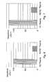
- FIGS. 3A to 3Fare schematic cross-section views showing steps to use the apparatus in FIG. 2 to form a lamination film using a Co complex containing ⁇ -diketone ligands over Cu wirings of dual damascene structure, according to an embodiment of the present invention.
- FIG. 4is a schematic plan view showing the configuration of an apparatus capable of forming Ru and Cu films using Ru and Cu complexes containing ⁇ -diketone ligands, according to an embodiment to the present invention.
- FIGS. 5A to 5Fare schematic cross-section views showing steps to use the apparatus in FIG. 2 to form a lamination film of Ru and Cu films using Ru and Cu complexes containing ⁇ -diketone ligands over Cu wirings of dual damascene structure, according to an embodiment of the present invention.
- FIG. 6is a graph showing the dependence of resistivity on plasma gas when a Co film was formed by the ALD method using a Co complex containing ⁇ -diketone ligands according to an embodiment of the present invention.
- FIG. 7is a graph showing the dependence of resistivity on plasma gas when a Ru film was formed by the ALD method using a Ru complex containing ⁇ -diketone ligands according to an embodiment of the present invention.
- FIG. 8is a graph showing the relationship of resistivity and nitrogen gas flow rate in an embodiment of the present invention.
- FIG. 9is a graph showing the dependence of resistivity on reactant gas when a Cu film was formed by the ALD method using a Cu complex containing ⁇ -diketone ligands according to an embodiment of the present invention.
- FIG. 10is a schematic explanation drawing showing the mechanism of how a single metal film is formed from a metal complex containing ⁇ -diketone ligands according to an embodiment of the present invention.
- FIGS. 11A , 11 B and 11 Cshow the chemical structures of Cu complexes containing ⁇ -diketone ligands that can be used in an embodiment of the present invention.
- FIG. 12is a graph showing the composition profile in the depth direction of a layer structure constituted by a TaN film and a metal layer laminated on top formed by a Ru complex containing ⁇ -diketone ligands according to an embodiment of the present invention.
- An embodiment of the present inventionprovides a method of forming a single-metal film on a substrate by plasma atomic layer deposition (ALD), comprising: (i) contacting a surface of a substrate with a ⁇ -diketone metal complex in a gas phase, whereby molecules of the ⁇ -diketone metal complex are attached to the surface of the substrate; (ii) exposing the molecule-attached surface to a nitrogen-hydrogen mixed plasma, thereby forming an atomic layer of the metal; and (iii) repeating steps (i) and (ii) for a next atomic layer on top of the atomic layer in step (ii), thereby accumulating the atomic layers to form the single-metal film on the substrate.
- ALDplasma atomic layer deposition
- the ⁇ -diketone metal complexcan easily be adsorbed onto any surface, and the nitrogen-hydrogen plasma can quickly and completely cleave the coordinate bonds between the metal and the ⁇ -diketone(s), thereby efficiently forming the single-metal film.
- no other ligand-supplying compoundsare used, or no other plasma is used.
- embodimentsinclude, but are not limited to, the followings:
- the single-metal filmis an elemental metal film.
- the nitrogen-hydrogen mixed plasmamay be produced by supplying a gas containing nitrogen and hydrogen, followed by applying RF power to the gas.
- the gas containing nitrogen and hydrogenmay be a mixture of nitrogen gas and hydrogen gas.
- a volumetric ratio of nitrogen to the gas mixturemaybe 1/100 to 50/100.
- the metal constituting the ⁇ -diketone metal complexmay be selected from the group consisting of metals belonging to Group 8, 1B, and 2B in the periodic chart.
- the metalmay be selected from the group consisting of Ru, Co, Pd, Pt, and Ir.
- the metalmay be Cu.
- the ⁇ -diketone metal complexmay be constituted by three ⁇ -diketones coordinated to a metal in its molecule.
- the ⁇ -diketone metal complexmay have only ⁇ -diketone(s) (optionally substituted) coordinated to a metal in its molecule.
- the methodmay further comprise forming a Cu film on the single-metal film.
- the Cu filmmay be formed using the single-metal film formed by steps (i) to (iii) as a Cu seed layer.
- steps (i) and (ii)may be repeated at least 10 times.
- steps (i) and (ii)may be repeated until a thickness of the single-metal film reaches at least 0.4 to 0.5 nm.
- the surface of the substrate on which the single-metal film is formedmay be constituted by a Cu barrier layer.
- steps (i) and (ii)may be conducted at a temperature of 300° C. or lower.
- the methodmay further comprise purging the ⁇ -diketone metal complex gas after step (i) and purging the gas containing nitrogen and hydrogen after step (ii).
- the nitrogen-hydrogen plasmamay be the only plasma to which the molecule-attached surface is exposed in step (ii).
- the ⁇ -diketone metal complexmay be the only metal compound contacting the surface of the substrate in step (i).
- the single-metal filmmay have a purity of 99% or higher.
- the surface of the substrate on which the single-metal film is formedmay have trenches and the single-metal film covers the trenches as a conformal coating.
- an organic metal complex containing ⁇ -diketone ligandsBy causing an organic metal complex containing ⁇ -diketone ligands to be adsorbed onto a substrate and then processing this substrate using a gas containing at least hydrogen atoms and nitrogen atoms that have been activated by high frequency, ⁇ -diketone ligands can be removed efficiently.
- These hydrogen atoms and nitrogen atomscan be supplied by the same molecule, or by different molecules. Unless a special circumstance exists, however, even a normal mixture gas of hydrogen gas and nitrogen gas can remove ⁇ -diketone ligands with sufficient effect.
- metal elements that can be coordinated to ⁇ -diketone and usable in an embodiment of the present inventiondesirable examples include 8B, 1B and 2B family elements, or typically Fe, Ni, Rh, Pd, Ir, Pt, Co, Ru and Cu, among others, where each of the foregoing metals can have least one, or even two, three or more ⁇ -diketone coordinated to it.
- a metal film of high purity(such as 99% or more, or even 99.9% or more in which case the film virtually consists of the applicable metal only) can be formed that does not easily produce nitrides when exposed to hydrogen/nitrogen plasma.
- Typical metal complexes coordinated to ⁇ -diketoneinclude tridipivaloylmathanatocobalt (DPM 3 CO), tridipivaloylmathanatoruthenium (DPM 3 Ru) and copper hexafluoroacetylacetonate trimethylvinylsilane (Cu(hfac)tmvs) ( FIG. 11A ), among others, and other copper complexes having the structures shown in FIGS. 11B and 11C are also available.
- the present inventionis not limited in any way to these metal complexes.
- basically organic metal complexes where only ⁇ -diketone is coordinatedare favorable because they can eliminate ligands more effectively through hydrogen/nitrogen plasma.
- the organic metal complexcan have a different ligand or ligands other than ⁇ -diketone.
- Ru complexetc., for example, the compounds described in U.S. Patent Application Publication No. 2008/0054472 and No. 2008/0124484 and U.S. patent application Ser. No. 12/203,405 owned by the same assignee as in the present application (the disclosure of each of which is herein incorporated by reference in its entirety with regard to metal complexes), among others, can be used in an embodiment, in addition to the compounds mentioned above.
- metal elements having one or more ⁇ -diketone coordinated to themother than the metal elements mentioned above, such as Ti, Ta, Hf, Nb, Mo, W, Mn, Mg, Sr, Ba and La, can be used in an embodiment.
- a metal layer (single metal layer) constituted by a ⁇ -diketone coordinated metal complexcan be formed in combination with other metal layer, for example, by using a Cu barrier film as the foundation layer.
- a metal layer constituted by a ⁇ -diketone coordinated copper complexcan be formed as a Cu seed film provided before a Cu film is formed.
- any known Cu barrier film or other appropriate filmcan be used.
- PVD-TaN and CVD-Ru, as well as other films produced by ALDsuch as WNC, WN, TaN, RuTaN, RuTa, TaNC, RuTaNC, TiN, RuTiN and RuTi, can be used.
- films that can be combined in a favorable manner with a metal layer constituted by ⁇ -diketone coordinated metal complexinclude, for example, the metal films and alloy films described in U.S. patent application Ser. Nos. 12/203,405 and Ser. No. 12/201,434 owned by the same assignee as in the present application (the disclosure of each of which is herein incorporated by reference in its entirety with regard to metal films).
- the aforementioned combinations with metal films by ADL methodare desirable because they allow the films to be formed continuously in the same reaction chamber and also offer excellent adhesion.
- a single metal layercan be formed directly on the substrate surface.
- the present inventioncovers all surfaces without limitation, as long as a ⁇ -diketone coordinated metal complex can be adsorbed onto the surface.
- a Cu seed layeris formed, for example.
- This Cu seed layercan be formed by PVD, etc., or according to an embodiment of the present invention using a ⁇ -diketone coordinated Cu complex.
- Ru and Cooffer excellent adhesion to Cu and therefore allow the single metal layer and Cu seed layer to be formed continuously on top of a Cu barrier film.
- the single metal layer in the aforementioned structureconsists of one layer.
- metal elements other than those in the 8B, 1B and 2B families(such as Ta) form nitrides when exposed to nitrogen/hydrogen plasma, even when nitrogen/hydrogen plasma severs ⁇ -diketone ligands, in which case the resulting film does not have a metal purity of 99% or more even when only one type of metal is used.
- the thickness of this single metal layervaries depending on the application, but in an embodiment it is in a range of 0.5 to 100 nm (or 1 nm or more but 20 nm or less, such as in a range of 1 to 10 nm or 5 to 20 nm, in an embodiment). If the film is too thin, the single metal layer cannot demonstrate its properties. Theoretically the film thickness can be increased infinitely. The severance of ⁇ -diketone ligands by nitrogen/hydrogen plasma occurs much more quickly and reliably compared to, say, when hydrogen plasma alone is used.
- the resistivityis not more than 5 times, or not more than twice, the resistivity of a bulk film formed by the same metal. In typical examples, the resistivity is 50 ⁇ cm or less, or even 20 ⁇ cm or less.
- the resistivity of a single metal layeris slightly higher than that of a bulk film (complete crystallization), this is because the single metal layer is thin and the film forming temperature is low, or 300° C. or below, and therefore complete crystallization cannot be achieved as in the case of a bulk film. In other words, the resistivity can be lowered by heat-treating the single metal layer at high temperature.
- the aforementioned resistivity valuesassume use of no high-temperature treatment.
- H 2 /N 2 plasma and H 2 plasma conditionsare listed below:
- N 2 /(N 2 +H 2 ) ratio1/100 to 50/100
- RF frequency1 to 30 MHz
- N 2 /(N 2 +H 2 ) ratiomentioned above, surprisingly even only a small amount of N 2 causes significant changes in film quality, and in an embodiment, sufficient effects can be achieved as long as the N 2 /(N 2 +H 2 ) ratio is 1/1000 or more.
- NH 3 plasmacan also be used (such as at 10 to 200 sccm) instead of H 2 /N 2 plasma.
- cycle conditions under which to introduce a ⁇ -diketone coordinated metal complex and to cause it to adsorb onto the substrate surfacecan be set as follows in an embodiment, although specific conditions vary depending on the type of ⁇ -diketone coordinated metal complex:
- Substrate temperature250 to 300° C.
- the purge conditions using an inert gascan be set as follows, for example:
- FIG. 1shows the steps to implement the ALD metal film forming method using an organic metal complex containing ⁇ -diketone ligands according to an embodiment of the present invention.
- the ALD processconsisting of steps 1000 to 1010 forms a metal film. The steps according to this embodiment are explained one by one using FIG. 1 .
- a substrateis introduced to an ALD apparatus that has been evacuated, and the substrate temperature is set to and stabilized at a specified level, after which the ALD process is started. Normally, first an organic metal complex containing ⁇ -diketone ligands is introduced onto the substrate, and then the organic metal complex coordinated by a ⁇ -diketone complex is discharged. This discharge is preferably be implemented in such a way that an inert gas is introduced under evacuation to discharge the gas of this organic metal complex from the reaction chamber.
- steps 1003 to 1007are repeated to achieve a specified film thickness ( 1008 ).
- this methodforms approx. 0.5 ⁇ of metal film of per cycle, which means that a metal film having the required film thickness can be formed after 20 to 100 cycles or so.
- the atmosphereis evacuated sufficiently and then the substrate is transferred out of the ALD apparatus, upon which the process ends. Needless to say, if the next process is performed in vacuum, then the substrate is also transferred in vacuum.
- FIG. 10shows the mechanism of how an atomic layer is formed in an embodiment of the present invention. Shown here is an example of a complex where ⁇ -diketone is coordinated to two metals (M). The ⁇ -diketone coordinated metal complex is adsorbed onto the substrate, after which nitrogen/hydrogen plasma is used to sever the ligand bonds between the metals and ⁇ -diketone, thereby virtually causing metal alone to be deposited onto the substrate. ⁇ -diketone that has been severed from the ligand bonds then bonds with nitrogen/hydrogen and is thus purged from the reaction chamber.
- Mmetals
- the deposition rate of metal atomsreaches as much as twice the rate achieved when hydrogen plasma is used, in which case the number of cycles needed to form one atomic layer is reduced to about a half.
- the deposited metal atomshave been fully separated from ⁇ -diketone and do not have any other bond, which allows a virtually pure metal layer to be formed.
- a metal layer having low resistivitycan be achieved.
- some metals such as Tahave the property to easily bond with nitrogen even after ⁇ -diketone has been separated reliably and quickly.
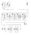
- FIG. 2shows an ALD apparatus for forming a metal film using an organic metal complex containing ⁇ -diketone ligands.
- This apparatuscomprises a reactor 301 in which a substrate heating base 303 , evacuation 304 , shower head 302 , gas introduction pipe 307 connected to the shower head, substrate 306 , exhaust pipe 304 and pressure regulation valve 305 are housed.
- the gas introduction systemcomprises a system to supply the first organic metal complex containing ⁇ -diketone ligands, system to supply the second organic metal material, H 2 gas supply, N 2 gas supply and Ar gas supply system.
- 319represents an APR, or Auto Pressure Regulator, which is used to control the pressure on the secondary side at a specified level.
- 320represents a MFC (Mass Flow Controler) used to control the flow rate at a constant level.
- the system to supply the first organic metal complex containing ⁇ -diketone ligandsis indicated by 325 , which is loaded in a material tank 324 and comprised of an Ar gas introduction valve 322 , bypass valve 321 and material supply valve 323 .
- 309represents a valve to introduce organic metal complex containing ⁇ -diketone ligands, while 310 represents an orifice and 308 represents a valve to introduce argon gas for dilution or purge.
- valve 309opens and the material is then fed to the gas introduction pipe 307 through a specified gas introduction hole in the orifice at an appropriate flow rate according to the pressure set by the APR 319 .
- H 2 , N 2 and Ar gas supply systemsare explained using FIG. 4 .
- gases supplied by pulsing actions and applied in the plasma ALD process333 , 335 and 337 each representing an APR (Auto Pressure Control) and 334 , 336 and 338 each representing a MFC (Mass Flow Control) are connected in series, respectively, just like the system to supply organic metal complex containing ⁇ -diketone ligands, where each pair of APR and MFC is connected to gas introduction valves 314 , 316 and 318 .
- Orifices 315 , 317are installed in the hydrogen and nitrogen lines, where each orifice has an introduction hole to allow a specified supply flow rate to be achieved quickly.
- No orificeis shown for the introduction valve denoted by 318 , but it is effective to also install an orifice at this valve if a specified supply flow rate is to be achieved quickly.
- the configurations of the ALD apparatus and gas systemsneed not be the same as those mentioned above, and any other configuration can be used as long as it is designed for a similar purpose, and such other configuration can also achieve a similar effect.
- FIGS. 3A to 3Fillustrate an example of steps constituting a wiring forming method in which a Co film is formed on top of a PVD-TaN barrier film, after which a Cu film is formed by PVD, and then a Cu film is formed by electroplating.
- the ALD method using an organic metal complex containing Co having ⁇ -diketone ligands, and plasma generated by a mixture gas of hydrogen and nitrogencan be used to form a Co film as shown in FIG. 3C .
- a Cu diffusion barrier insulation film 102 , inter-layer insulation film 103 , etching stopper film 104 , inter-layer insulation film 105 and etching stopper film 106are laminated on a bottom-layer Cu wiring 101 , and a via hole 107 and wiring 108 are also present in the dual damascene structure.
- a Cu diffusion barrier film 109is formed. This diffusion barrier can be formed by the PVD method, or by the CVD method or ALD method.
- a material containing ⁇ -diketone group ligandssuch as tridipivaloylmathanatocobalt (DPM 3 CO) is supplied onto this Cu diffusion barrier film, after which a mixture gas of hydrogen and nitrogen is used to form a Co film 110 via ALD according to the sequence shown in FIG. 1 .
- a Cu film 111is formed, for example, by the PVD method, and this film is used as a seed layer to form a Cu film 112 via electroplating in FIG. 3E , after which the Cu film is flattened by CMP and a Cu wiring 113 is formed in FIG. 3F .
- a Co layercan be formed underneath the Cu film, which achieves good adhesion between the Cu film and the layer below it and therefore high reliability can be ensured.
- FIG. 4shows an apparatus applied to the forming of a Ru/Cu lamination structure using Ru and Cu complexes containing ⁇ -diketone ligands.
- This apparatuscomprises a cluster apparatus 500 , wafer cassette loader 501 , atmospheric transfer robot 502 , load lock chamber 503 , vacuum transfer robot 504 , pre-processing reactor 506 , barrier metal forming reactor 505 and Cu/Ru lamination forming reactor 507 , while other components include an argon gas supply system 508 , Cu material supply system 509 , Ru material supply system 510 , H 2 gas supply system 511 , N 2 gas supply 515 , Cu material supply line 512 , Co material supply line 513 , H 2 gas supply line 512 and N 2 gas supply line 516 .
- FIGS. 5A to 5Fshow the steps to continuously form a barrier metal, Ru film and Cu film in a dual damascene wiring structure using the apparatus shown in FIG. 4 .
- a Cu diffusion barrier insulation film 402 , inter-layer insulation film 403 , etching stopper film 404 , inter-layer insulation film 405 and etching stopper film 406are laminated on a bottom-layer Cu wiring 401 , and a via hole 407 and wiring 408 are also present in the dual damascene structure.
- FIG. 5Bfirst a Cu diffusion barrier film 409 is formed. This diffusion barrier can be formed by the PVD method, or by the CVD method or ALD method.
- FIG. 5Ashows the steps to continuously form a barrier metal, Ru film and Cu film in a dual damascene wiring structure using the apparatus shown in FIG. 4 .
- a Ru film 410is formed on top of this Cu diffusion barrier film 409 , after which a Cu film 411 is formed in FIG. 5D .
- a Cu film 412is formed via electroplating, after which the film is flattened by CMP in FIG. 5F and a Cu wiring 413 is formed.
- a material containing ⁇ -diketone group ligandssuch as tridipivaloylmathanatoruthenium (DPM 3 Ru) is supplied onto this Cu diffusion barrier film 409 , after which a mixture gas of hydrogen and nitrogen is used to form a Ru film 410 via ALD according to the sequence shown in FIG. 1 .
- a material containing ⁇ -diketone group ligandssuch as Cu(hfac)tmvs, is used and a mixture gas of hydrogen and nitrogen is used to form a Cu film 411 via ALD. Since the Cu seed layer and the layer below it can both be formed as atomic layers using ⁇ -diketone metal complexes, good adhesion to the Cu film can be achieved and low resistivity and high reliability can be ensured.
- the substrateis transferred to 506 via the cassette loader 501 , and in 506 the surface of the bottom-layer Cu wiring 401 at the via hole 407 is reduced by hydrogen plasma, after which the substrate is transported to the processing chamber 505 and a copper diffusion barrier metal film is formed.
- This metal filmcan be formed by the PVD method, CVD method or ALD method.
- the specific filmis a TaN, RuTaN, TiN, RuTiN or other metal film that serves as a Cu diffusion barrier.
- the substrateis transferred to the processing chamber 507 , where a Ru material constituted by a metal complex containing ⁇ -diketone ligands is evaporated and supplied to form an extremely thin Ru film of 1 to 2 nm in thickness through the cycle shown in FIG. 1 .
- a Cu material constituted by a metal complex containing ⁇ -diketone ligandsis evaporated and supplied to form a Cu film of 1 to 10 nm in thickness through the cycle shown in FIG. 1 .
- both Ru and Cu filmscan be formed in the same module. This way, a Cu/Ru lamination film can be formed via ALD at the same low temperature. This is possible because, by using plasma generated by a mixture gas of hydrogen and nitrogen, Ru and Cu films can be formed easily at low temperature. Similarly, these Ru and Cu layers can also be formed repeatedly to form a structure of mixed Ru/Cu layers.
- FIG. 2a process of forming a Co film is illustrated.
- an inter-layer connection structure using a Co filmwas formed according to the steps shown in FIGS. 3A to 3F .
- the heating base 303 in the processing chamber 301was set to 300° C.
- the Co material 325or tridipivaloylmathanatocobalt (DPM 3 CO), was filled in a bottle 324 and this bottle was heated to 120° C.
- This Co material 325had a vapor pressure of 0.5 torr, and vapor of the Co material was supplied by an argon carrier gas to a substrate via a valve 309 and orifice 310 .
- this Co materialwas purged by the argon gas supplied from a valve 318 , after which N 2 was supplied by 50 sccm from a valve 316 and orifice 317 , followed by the supply of H 2 by 200 sccm from a valve 314 and orifice 315 .
- High frequency power of 200 to 500 W and 13.56 MHzwas then applied to this mixture gas and the excited plasma was used to eliminate ⁇ -diketone ligands from the Co material molecules having ⁇ -diketone ligands and adsorbed onto the substrate.
- the plasma application timevaries depending on the high-frequency output, good reaction could be achieved after approx. 1 to 3 seconds at 400 W.
- FIG. 6shows the relative resistance levels obtained when only H 2 plasma was used and a mixture gas of H 2 and N 2 was used. As shown, the resistivity dropped to 1/5 under the same plasma condition (400 W) and plasma application time (3 seconds).
- the substratewas transferred from the reactor to the next process, or Cu forming process, where the steps in FIGS. 3E and 3F were implemented.
- an inter-layer connection structurewas formed through the procedure shown in FIGS. 5A to 5F using a process of forming Ru and Cu films continuously in the same reaction chamber.
- one material 325is a Ru material containing ⁇ -diketone ligands
- the other material 332is a Cu material containing ⁇ -diketone ligands.
- a substratewas transferred to the reaction chamber, and first in FIG. 2 the heating base 303 in the processing chamber 301 was set to 300° C.
- the Ru material, or tridipivaloylmathanatoruthenium (DPM 3 Ru) 325was filled in a bottle 324 , and this bottle was heated to 120° C.
- This Ru material 325had a vapor pressure of 0.1 torr, and vapor of the Ru material was supplied by an argon carrier gas to the substrate via a valve 309 and orifice 310 .
- this Ru materialwas purged by the argon gas supplied from a valve 318 , after which N 2 was supplied by 50 sccm from a valve 316 and orifice 317 , followed by the supply of H 2 by 200 sccm from avalve 314 and orifice 315 .
- High frequency power of 200 to 500 W and 13.56 MHzwas then applied to this mixture gas and the excited plasma was used to eliminate ⁇ -diketone ligands from the Ru material molecules having ⁇ -diketone ligands and adsorbed onto the substrate.
- the plasma application timevaries depending on the high-frequency output, good reaction could be achieved after approx. 5 to 15 seconds at 400 W.
- FIG. 7shows the resistivity levels obtained when only H 2 plasma was used and a mixture gas of H 2 and N 2 was used. As shown, the resistivity dropped to approx. 1/5 when the H2/N2 mixture gas was used.
- FIG. 8shows the resistivity levels achieved when the flow rate of nitrogen was changed from 0 to 200 sccm at a constant hydrogen flow rate of 400 sccm. Since the resistivity dropped substantially when only 4 sccm of N 2 gas was introduced, it can be said that adding a small amount of N 2 to plasma would eliminate ⁇ -diketone ligands. Accordingly, sufficient elimination effects can be demonstrated as long as the flow rate of N 2 gas is 1% or more relative to the flow rate of H 2 gas.
- a Cu material 332or Cu(hfac)tmvs (copper hexafluoroacetylacetonate trimethylvinylsilane), was heated to 80° C. and supplied to form a Cu film 411 according to the sequence shown in FIG. 1 .
- the Cu material 332was filled in a bottle 331 , and this bottle was heated to 800° C.
- This Cu material 325had a vapor pressure of 0.5 torr or more, and vapor of the Cu material was supplied by an argon carrier gas to the substrate via a valve 312 and orifice 313 .
- this Cu materialwas purged by the argon gas supplied from a valve 318 , after which N 2 was supplied by 50 sccm from a valve 316 and orifice 317 , followed by the supply of H 2 by 200 sccm from a valve 314 and orifice 315 .
- High frequency power of 200 to 500 W and 13.56 MHzwas then applied to this mixture gas and the excited plasma was used to eliminate ⁇ -diketone ligands from the Cu material molecules having ⁇ -diketone ligands and adsorbed onto the substrate.
- the plasma application timevaries depending on the high-frequency output, good reaction could be achieved after approx. 5 to 15 seconds at 400 W. Whether this reaction is acceptable or not can be determined from the resistivity of the formed Cu film.
- the Cu film obtained under the above conditionshad a resistivity of 2 ⁇ cm or less.
- FIG. 9compares the resistivity of a Cu film deposited using H 2 plasma alone against the resistivity of a Cu film deposited using a mixture gas of H 2 and N 2 . As shown, the resistivity could be dropped to approx. 1/5 using the H 2 /N 2 mixture gas.
- the film deposition ratevaries depending on the plasma output, it is 0.1 to 0.5 ⁇ per cycle, or preferably 0.5 ⁇ per cycle. In other words, 1 to 5 nm of film needed as a Cu seed layer can be obtained after 20 to 100 cycles.
- a Cu film 412can be formed on top of this Cu film 411 ( FIG. 5D ) via electroplating.
- a mixed layer structure constituted by multiple Ru and Cu layerscan also be formed by alternating the Ru ALD cycle and Cu ALD cycle.
- the good Cu electroplating propertyallowed complete burying by Cu plating of via holes of 30 nm or less in diameter in a structure of 5 to 10 in aspect ratio.
- This exampleillustrates a process of forming a RuTaN film as a Cu barrier layer and then forming Ru and Cu layers.
- one material 325is a Ru material containing ⁇ -diketone ligands, while the other material 332 is a Ta organic metal material.
- a substratewas transferred to the reaction chamber, and first in FIG. 2 the heating base 303 in the processing chamber 301 was set to 300° C.
- the Ta material, or TAIMATAtertiaryamylimidotris(dimethylamido)tantalum
- Taimatawas supplied by an Ar carrier gas from a bottle 331 heated to 80° C.
- 50 sccm of N 2was supplied from a valve 316 and orifice 317
- 200 sccm of H 2was supplied from a valve 314 and orifice 315 .
- this Ru materialwas purged by the argon gas supplied from a valve 318 , after which N 2 was supplied by 50 sccm from a valve 316 and orifice 317 , followed by the supply of H 2 by 200 sccm from a valve 314 and orifice 315 .
- High frequency power of 200 to 500 W and 13.56 MHzwas then applied to this mixture gas and the excited plasma was used to eliminate ⁇ -diketone ligands from the Ru material molecules having ⁇ -diketone ligands adsorbed onto the substrate.
- the plasma application timevaries depending on the high-frequency output, good reaction could be achieved after approx. 5 to 15 seconds at 400 W.
- This Ru material supply stepwas repeated twice, after which the Ta material was supplied again and the plasma processing step using H 2 /N 2 gas was performed once. In the same manner, the “Ru supply step ⁇ 2+Plasma step” cycle was repeated 14 times. As a result, 2 nm of RuTaN film was formed.
- the Ru film obtained under the above conditionshad a resistivity of 30 ⁇ cm or less. This suggests that impurities arising from the Ru material could be reduced and a Ru metal film 410 of low resistivity ( FIG. 5C ) was formed.
- the RBS analysis results shown in FIG. 12were obtained by forming a RuTaN alloy of 2 nm in thickness according to the method explained above, forming a Ru film of 10 nm in thickness, and then analyzing the composition using the Rutherford backscattering method.
- the schematic cross-section view of the trench shown in FIG. 12also indicates a PVD-Cu seed layer at the top, the composition was analyzed when the Ru film was laminated on top of the RuTaN film formed as a Cu barrier layer. With any Ru film, it is difficult to analyze the composition unless the film thickness is approx. 10 nm, because oxygen and carbon in atmosphere adsorb to the Ru surface.
- the amount of carbon and oxygen that entered the Ru filmis only 1 atomic % or less, and the Ru film is at least 99% pure.
- a Ru film containing less impurities and offering low resistivitycan be formed. From the trend of thickness of formed film, the Ru deposition rate per cycle when H 2 /N 2 plasma was used was twice the rate achieved when H 2 plasma was used, suggesting that the decomposition of the Ru organic metal material coordinated by ⁇ -diketone was significantly promoted by the use of plasma generated by a H 2 /N 2 mixture gas.
- This Ru layerwas typically formed by 1 to 2 nm, and approx. 5 to 20 nM of Cu layer to serve as a seed layer for Cu deposition was formed on top of this Ru layer via electroplating. It was confirmed that this Cu layer could be formed continuously without causing the Cu layer to agglomerate over the Ru layer at the bottom, regardless of whether the PVD method, CVD method or ALD method was used. In other words, the Ru layer demonstrated good adhesion to Cu and was suitable for the formation of a continuous Cu layer. It was also confirmed that, by forming a Cu film via electroplating on top of this Cu layer, sufficient burying property could be achieved using this Cu film via electroplating even with wiring structures having wiring widths of 20 to 50 nm and aspect ratios of approx.
- the Ru film achieved by the method explained in this exampleis very effective in the formation of Cu seed layers as mentioned above as well as in the formation of fine Cu wirings via electroplating.
- a method for forming metal film by plasma atomic layer depositionwherein said method includes steps to cause an organic metal complex containing ⁇ -diketone ligands to be chemically adsorbed onto a substrate, after which the substrate is processed using a gas containing at least hydrogen atoms and nitrogen atoms that have been activated, to form a metal layer from metal atoms constituting the aforementioned organic metal complex.
Landscapes
- Chemical & Material Sciences (AREA)
- Engineering & Computer Science (AREA)
- Metallurgy (AREA)
- General Chemical & Material Sciences (AREA)
- Chemical Kinetics & Catalysis (AREA)
- Materials Engineering (AREA)
- Mechanical Engineering (AREA)
- Organic Chemistry (AREA)
- Plasma & Fusion (AREA)
- Electromagnetism (AREA)
- Physics & Mathematics (AREA)
- Internal Circuitry In Semiconductor Integrated Circuit Devices (AREA)
- Chemical Vapour Deposition (AREA)
Abstract
Description
Claims (16)
Priority Applications (1)
| Application Number | Priority Date | Filing Date | Title |
|---|---|---|---|
| US12/251,343US8133555B2 (en) | 2008-10-14 | 2008-10-14 | Method for forming metal film by ALD using beta-diketone metal complex |
Applications Claiming Priority (1)
| Application Number | Priority Date | Filing Date | Title |
|---|---|---|---|
| US12/251,343US8133555B2 (en) | 2008-10-14 | 2008-10-14 | Method for forming metal film by ALD using beta-diketone metal complex |
Publications (2)
| Publication Number | Publication Date |
|---|---|
| US20100092696A1 US20100092696A1 (en) | 2010-04-15 |
| US8133555B2true US8133555B2 (en) | 2012-03-13 |
Family
ID=42099092
Family Applications (1)
| Application Number | Title | Priority Date | Filing Date |
|---|---|---|---|
| US12/251,343Active2029-10-13US8133555B2 (en) | 2008-10-14 | 2008-10-14 | Method for forming metal film by ALD using beta-diketone metal complex |
Country Status (1)
| Country | Link |
|---|---|
| US (1) | US8133555B2 (en) |
Cited By (2)
| Publication number | Priority date | Publication date | Assignee | Title |
|---|---|---|---|---|
| US20100320607A1 (en)* | 2007-02-26 | 2010-12-23 | Tokyo Electron Limited | Interconnect structures with a metal nitride diffusion barrier containing ruthenium |
| US20130059078A1 (en)* | 2010-02-23 | 2013-03-07 | Julien Gatineau | Use of ruthenium tetroxide as a precursor and reactant for thin film depositions |
Families Citing this family (373)
| Publication number | Priority date | Publication date | Assignee | Title |
|---|---|---|---|---|
| US7858144B2 (en)* | 2007-09-26 | 2010-12-28 | Eastman Kodak Company | Process for depositing organic materials |
| JP5377489B2 (en)* | 2008-07-18 | 2013-12-25 | 株式会社アルバック | Method for forming Cu wiring film |
| US10378106B2 (en) | 2008-11-14 | 2019-08-13 | Asm Ip Holding B.V. | Method of forming insulation film by modified PEALD |
| US9394608B2 (en) | 2009-04-06 | 2016-07-19 | Asm America, Inc. | Semiconductor processing reactor and components thereof |
| US8802201B2 (en) | 2009-08-14 | 2014-08-12 | Asm America, Inc. | Systems and methods for thin-film deposition of metal oxides using excited nitrogen-oxygen species |
| US9312155B2 (en) | 2011-06-06 | 2016-04-12 | Asm Japan K.K. | High-throughput semiconductor-processing apparatus equipped with multiple dual-chamber modules |
| US10364496B2 (en) | 2011-06-27 | 2019-07-30 | Asm Ip Holding B.V. | Dual section module having shared and unshared mass flow controllers |
| US10854498B2 (en) | 2011-07-15 | 2020-12-01 | Asm Ip Holding B.V. | Wafer-supporting device and method for producing same |
| US20130023129A1 (en) | 2011-07-20 | 2013-01-24 | Asm America, Inc. | Pressure transmitter for a semiconductor processing environment |
| US9017481B1 (en) | 2011-10-28 | 2015-04-28 | Asm America, Inc. | Process feed management for semiconductor substrate processing |
| US9558931B2 (en) | 2012-07-27 | 2017-01-31 | Asm Ip Holding B.V. | System and method for gas-phase sulfur passivation of a semiconductor surface |
| US9659799B2 (en) | 2012-08-28 | 2017-05-23 | Asm Ip Holding B.V. | Systems and methods for dynamic semiconductor process scheduling |
| US9021985B2 (en) | 2012-09-12 | 2015-05-05 | Asm Ip Holdings B.V. | Process gas management for an inductively-coupled plasma deposition reactor |
| US10714315B2 (en) | 2012-10-12 | 2020-07-14 | Asm Ip Holdings B.V. | Semiconductor reaction chamber showerhead |
| US20160376700A1 (en) | 2013-02-01 | 2016-12-29 | Asm Ip Holding B.V. | System for treatment of deposition reactor |
| US9484191B2 (en) | 2013-03-08 | 2016-11-01 | Asm Ip Holding B.V. | Pulsed remote plasma method and system |
| US9589770B2 (en) | 2013-03-08 | 2017-03-07 | Asm Ip Holding B.V. | Method and systems for in-situ formation of intermediate reactive species |
| US8993054B2 (en) | 2013-07-12 | 2015-03-31 | Asm Ip Holding B.V. | Method and system to reduce outgassing in a reaction chamber |
| US9240412B2 (en) | 2013-09-27 | 2016-01-19 | Asm Ip Holding B.V. | Semiconductor structure and device and methods of forming same using selective epitaxial process |
| US9605343B2 (en) | 2013-11-13 | 2017-03-28 | Asm Ip Holding B.V. | Method for forming conformal carbon films, structures conformal carbon film, and system of forming same |
| US10683571B2 (en) | 2014-02-25 | 2020-06-16 | Asm Ip Holding B.V. | Gas supply manifold and method of supplying gases to chamber using same |
| US10167557B2 (en) | 2014-03-18 | 2019-01-01 | Asm Ip Holding B.V. | Gas distribution system, reactor including the system, and methods of using the same |
| US11015245B2 (en) | 2014-03-19 | 2021-05-25 | Asm Ip Holding B.V. | Gas-phase reactor and system having exhaust plenum and components thereof |
| US9663857B2 (en)* | 2014-04-07 | 2017-05-30 | Asm Ip Holding B.V. | Method for stabilizing reaction chamber pressure |
| CA2949398C (en)* | 2014-06-13 | 2022-07-19 | Basf Coatings Gmbh | Process for producing organic-inorganic laminates |
| US10858737B2 (en) | 2014-07-28 | 2020-12-08 | Asm Ip Holding B.V. | Showerhead assembly and components thereof |
| US9890456B2 (en) | 2014-08-21 | 2018-02-13 | Asm Ip Holding B.V. | Method and system for in situ formation of gas-phase compounds |
| US10941490B2 (en) | 2014-10-07 | 2021-03-09 | Asm Ip Holding B.V. | Multiple temperature range susceptor, assembly, reactor and system including the susceptor, and methods of using the same |
| US9657845B2 (en) | 2014-10-07 | 2017-05-23 | Asm Ip Holding B.V. | Variable conductance gas distribution apparatus and method |
| KR102300403B1 (en) | 2014-11-19 | 2021-09-09 | 에이에스엠 아이피 홀딩 비.브이. | Method of depositing thin film |
| KR102263121B1 (en) | 2014-12-22 | 2021-06-09 | 에이에스엠 아이피 홀딩 비.브이. | Semiconductor device and manufacuring method thereof |
| US10529542B2 (en) | 2015-03-11 | 2020-01-07 | Asm Ip Holdings B.V. | Cross-flow reactor and method |
| US10276355B2 (en) | 2015-03-12 | 2019-04-30 | Asm Ip Holding B.V. | Multi-zone reactor, system including the reactor, and method of using the same |
| US10458018B2 (en) | 2015-06-26 | 2019-10-29 | Asm Ip Holding B.V. | Structures including metal carbide material, devices including the structures, and methods of forming same |
| US10600673B2 (en) | 2015-07-07 | 2020-03-24 | Asm Ip Holding B.V. | Magnetic susceptor to baseplate seal |
| US10043661B2 (en) | 2015-07-13 | 2018-08-07 | Asm Ip Holding B.V. | Method for protecting layer by forming hydrocarbon-based extremely thin film |
| US10083836B2 (en) | 2015-07-24 | 2018-09-25 | Asm Ip Holding B.V. | Formation of boron-doped titanium metal films with high work function |
| US10087525B2 (en) | 2015-08-04 | 2018-10-02 | Asm Ip Holding B.V. | Variable gap hard stop design |
| US9647114B2 (en) | 2015-08-14 | 2017-05-09 | Asm Ip Holding B.V. | Methods of forming highly p-type doped germanium tin films and structures and devices including the films |
| US9960072B2 (en) | 2015-09-29 | 2018-05-01 | Asm Ip Holding B.V. | Variable adjustment for precise matching of multiple chamber cavity housings |
| US10211308B2 (en) | 2015-10-21 | 2019-02-19 | Asm Ip Holding B.V. | NbMC layers |
| US10322384B2 (en) | 2015-11-09 | 2019-06-18 | Asm Ip Holding B.V. | Counter flow mixer for process chamber |
| US9627221B1 (en) | 2015-12-28 | 2017-04-18 | Asm Ip Holding B.V. | Continuous process incorporating atomic layer etching |
| US11139308B2 (en) | 2015-12-29 | 2021-10-05 | Asm Ip Holding B.V. | Atomic layer deposition of III-V compounds to form V-NAND devices |
| US10468251B2 (en) | 2016-02-19 | 2019-11-05 | Asm Ip Holding B.V. | Method for forming spacers using silicon nitride film for spacer-defined multiple patterning |
| US10529554B2 (en) | 2016-02-19 | 2020-01-07 | Asm Ip Holding B.V. | Method for forming silicon nitride film selectively on sidewalls or flat surfaces of trenches |
| US20170241019A1 (en)* | 2016-02-22 | 2017-08-24 | Ultratech, Inc. | Pe-ald methods with reduced quartz-based contamination |
| US10501866B2 (en) | 2016-03-09 | 2019-12-10 | Asm Ip Holding B.V. | Gas distribution apparatus for improved film uniformity in an epitaxial system |
| US10343920B2 (en) | 2016-03-18 | 2019-07-09 | Asm Ip Holding B.V. | Aligned carbon nanotubes |
| US9892913B2 (en) | 2016-03-24 | 2018-02-13 | Asm Ip Holding B.V. | Radial and thickness control via biased multi-port injection settings |
| US10190213B2 (en) | 2016-04-21 | 2019-01-29 | Asm Ip Holding B.V. | Deposition of metal borides |
| US10865475B2 (en) | 2016-04-21 | 2020-12-15 | Asm Ip Holding B.V. | Deposition of metal borides and silicides |
| US10087522B2 (en) | 2016-04-21 | 2018-10-02 | Asm Ip Holding B.V. | Deposition of metal borides |
| US10367080B2 (en) | 2016-05-02 | 2019-07-30 | Asm Ip Holding B.V. | Method of forming a germanium oxynitride film |
| US10032628B2 (en) | 2016-05-02 | 2018-07-24 | Asm Ip Holding B.V. | Source/drain performance through conformal solid state doping |
| KR102592471B1 (en) | 2016-05-17 | 2023-10-20 | 에이에스엠 아이피 홀딩 비.브이. | Method of forming metal interconnection and method of fabricating semiconductor device using the same |
| US11453943B2 (en) | 2016-05-25 | 2022-09-27 | Asm Ip Holding B.V. | Method for forming carbon-containing silicon/metal oxide or nitride film by ALD using silicon precursor and hydrocarbon precursor |
| US10388509B2 (en) | 2016-06-28 | 2019-08-20 | Asm Ip Holding B.V. | Formation of epitaxial layers via dislocation filtering |
| US10612137B2 (en) | 2016-07-08 | 2020-04-07 | Asm Ip Holdings B.V. | Organic reactants for atomic layer deposition |
| US9859151B1 (en) | 2016-07-08 | 2018-01-02 | Asm Ip Holding B.V. | Selective film deposition method to form air gaps |
| US9793135B1 (en) | 2016-07-14 | 2017-10-17 | ASM IP Holding B.V | Method of cyclic dry etching using etchant film |
| US10714385B2 (en) | 2016-07-19 | 2020-07-14 | Asm Ip Holding B.V. | Selective deposition of tungsten |
| KR102354490B1 (en) | 2016-07-27 | 2022-01-21 | 에이에스엠 아이피 홀딩 비.브이. | Method of processing a substrate |
| US9887082B1 (en) | 2016-07-28 | 2018-02-06 | Asm Ip Holding B.V. | Method and apparatus for filling a gap |
| US9812320B1 (en) | 2016-07-28 | 2017-11-07 | Asm Ip Holding B.V. | Method and apparatus for filling a gap |
| US10395919B2 (en) | 2016-07-28 | 2019-08-27 | Asm Ip Holding B.V. | Method and apparatus for filling a gap |
| US10177025B2 (en) | 2016-07-28 | 2019-01-08 | Asm Ip Holding B.V. | Method and apparatus for filling a gap |
| KR102532607B1 (en) | 2016-07-28 | 2023-05-15 | 에이에스엠 아이피 홀딩 비.브이. | Substrate processing apparatus and method of operating the same |
| US10090316B2 (en) | 2016-09-01 | 2018-10-02 | Asm Ip Holding B.V. | 3D stacked multilayer semiconductor memory using doped select transistor channel |
| US10410943B2 (en) | 2016-10-13 | 2019-09-10 | Asm Ip Holding B.V. | Method for passivating a surface of a semiconductor and related systems |
| US10643826B2 (en) | 2016-10-26 | 2020-05-05 | Asm Ip Holdings B.V. | Methods for thermally calibrating reaction chambers |
| US11532757B2 (en) | 2016-10-27 | 2022-12-20 | Asm Ip Holding B.V. | Deposition of charge trapping layers |
| US10714350B2 (en) | 2016-11-01 | 2020-07-14 | ASM IP Holdings, B.V. | Methods for forming a transition metal niobium nitride film on a substrate by atomic layer deposition and related semiconductor device structures |
| US10643904B2 (en) | 2016-11-01 | 2020-05-05 | Asm Ip Holdings B.V. | Methods for forming a semiconductor device and related semiconductor device structures |
| US10229833B2 (en) | 2016-11-01 | 2019-03-12 | Asm Ip Holding B.V. | Methods for forming a transition metal nitride film on a substrate by atomic layer deposition and related semiconductor device structures |
| US10435790B2 (en) | 2016-11-01 | 2019-10-08 | Asm Ip Holding B.V. | Method of subatmospheric plasma-enhanced ALD using capacitively coupled electrodes with narrow gap |
| US10134757B2 (en) | 2016-11-07 | 2018-11-20 | Asm Ip Holding B.V. | Method of processing a substrate and a device manufactured by using the method |
| KR102546317B1 (en) | 2016-11-15 | 2023-06-21 | 에이에스엠 아이피 홀딩 비.브이. | Gas supply unit and substrate processing apparatus including the same |
| US10340135B2 (en) | 2016-11-28 | 2019-07-02 | Asm Ip Holding B.V. | Method of topologically restricted plasma-enhanced cyclic deposition of silicon or metal nitride |
| KR102762543B1 (en) | 2016-12-14 | 2025-02-05 | 에이에스엠 아이피 홀딩 비.브이. | Substrate processing apparatus |
| US11581186B2 (en) | 2016-12-15 | 2023-02-14 | Asm Ip Holding B.V. | Sequential infiltration synthesis apparatus |
| US11447861B2 (en) | 2016-12-15 | 2022-09-20 | Asm Ip Holding B.V. | Sequential infiltration synthesis apparatus and a method of forming a patterned structure |
| US9916980B1 (en) | 2016-12-15 | 2018-03-13 | Asm Ip Holding B.V. | Method of forming a structure on a substrate |
| KR102700194B1 (en) | 2016-12-19 | 2024-08-28 | 에이에스엠 아이피 홀딩 비.브이. | Substrate processing apparatus |
| US10269558B2 (en) | 2016-12-22 | 2019-04-23 | Asm Ip Holding B.V. | Method of forming a structure on a substrate |
| US10867788B2 (en) | 2016-12-28 | 2020-12-15 | Asm Ip Holding B.V. | Method of forming a structure on a substrate |
| US11390950B2 (en) | 2017-01-10 | 2022-07-19 | Asm Ip Holding B.V. | Reactor system and method to reduce residue buildup during a film deposition process |
| US10655221B2 (en) | 2017-02-09 | 2020-05-19 | Asm Ip Holding B.V. | Method for depositing oxide film by thermal ALD and PEALD |
| US10468261B2 (en) | 2017-02-15 | 2019-11-05 | Asm Ip Holding B.V. | Methods for forming a metallic film on a substrate by cyclical deposition and related semiconductor device structures |
| US10283353B2 (en) | 2017-03-29 | 2019-05-07 | Asm Ip Holding B.V. | Method of reforming insulating film deposited on substrate with recess pattern |
| US10529563B2 (en) | 2017-03-29 | 2020-01-07 | Asm Ip Holdings B.V. | Method for forming doped metal oxide films on a substrate by cyclical deposition and related semiconductor device structures |
| US10103040B1 (en) | 2017-03-31 | 2018-10-16 | Asm Ip Holding B.V. | Apparatus and method for manufacturing a semiconductor device |
| USD830981S1 (en) | 2017-04-07 | 2018-10-16 | Asm Ip Holding B.V. | Susceptor for semiconductor substrate processing apparatus |
| KR102457289B1 (en) | 2017-04-25 | 2022-10-21 | 에이에스엠 아이피 홀딩 비.브이. | Method for depositing a thin film and manufacturing a semiconductor device |
| US10770286B2 (en) | 2017-05-08 | 2020-09-08 | Asm Ip Holdings B.V. | Methods for selectively forming a silicon nitride film on a substrate and related semiconductor device structures |
| US10446393B2 (en) | 2017-05-08 | 2019-10-15 | Asm Ip Holding B.V. | Methods for forming silicon-containing epitaxial layers and related semiconductor device structures |
| US10892156B2 (en) | 2017-05-08 | 2021-01-12 | Asm Ip Holding B.V. | Methods for forming a silicon nitride film on a substrate and related semiconductor device structures |
| US10504742B2 (en) | 2017-05-31 | 2019-12-10 | Asm Ip Holding B.V. | Method of atomic layer etching using hydrogen plasma |
| US10886123B2 (en) | 2017-06-02 | 2021-01-05 | Asm Ip Holding B.V. | Methods for forming low temperature semiconductor layers and related semiconductor device structures |
| US12040200B2 (en) | 2017-06-20 | 2024-07-16 | Asm Ip Holding B.V. | Semiconductor processing apparatus and methods for calibrating a semiconductor processing apparatus |
| US11306395B2 (en) | 2017-06-28 | 2022-04-19 | Asm Ip Holding B.V. | Methods for depositing a transition metal nitride film on a substrate by atomic layer deposition and related deposition apparatus |
| US10685834B2 (en) | 2017-07-05 | 2020-06-16 | Asm Ip Holdings B.V. | Methods for forming a silicon germanium tin layer and related semiconductor device structures |
| KR20190009245A (en) | 2017-07-18 | 2019-01-28 | 에이에스엠 아이피 홀딩 비.브이. | Methods for forming a semiconductor device structure and related semiconductor device structures |
| US11018002B2 (en) | 2017-07-19 | 2021-05-25 | Asm Ip Holding B.V. | Method for selectively depositing a Group IV semiconductor and related semiconductor device structures |
| US10541333B2 (en) | 2017-07-19 | 2020-01-21 | Asm Ip Holding B.V. | Method for depositing a group IV semiconductor and related semiconductor device structures |
| US11374112B2 (en) | 2017-07-19 | 2022-06-28 | Asm Ip Holding B.V. | Method for depositing a group IV semiconductor and related semiconductor device structures |
| US10605530B2 (en) | 2017-07-26 | 2020-03-31 | Asm Ip Holding B.V. | Assembly of a liner and a flange for a vertical furnace as well as the liner and the vertical furnace |
| US10312055B2 (en) | 2017-07-26 | 2019-06-04 | Asm Ip Holding B.V. | Method of depositing film by PEALD using negative bias |
| US10590535B2 (en) | 2017-07-26 | 2020-03-17 | Asm Ip Holdings B.V. | Chemical treatment, deposition and/or infiltration apparatus and method for using the same |
| TWI815813B (en) | 2017-08-04 | 2023-09-21 | 荷蘭商Asm智慧財產控股公司 | Showerhead assembly for distributing a gas within a reaction chamber |
| US10692741B2 (en) | 2017-08-08 | 2020-06-23 | Asm Ip Holdings B.V. | Radiation shield |
| US10770336B2 (en) | 2017-08-08 | 2020-09-08 | Asm Ip Holding B.V. | Substrate lift mechanism and reactor including same |
| US11769682B2 (en) | 2017-08-09 | 2023-09-26 | Asm Ip Holding B.V. | Storage apparatus for storing cassettes for substrates and processing apparatus equipped therewith |
| US11139191B2 (en) | 2017-08-09 | 2021-10-05 | Asm Ip Holding B.V. | Storage apparatus for storing cassettes for substrates and processing apparatus equipped therewith |
| US10249524B2 (en) | 2017-08-09 | 2019-04-02 | Asm Ip Holding B.V. | Cassette holder assembly for a substrate cassette and holding member for use in such assembly |
| US10236177B1 (en) | 2017-08-22 | 2019-03-19 | ASM IP Holding B.V.. | Methods for depositing a doped germanium tin semiconductor and related semiconductor device structures |
| USD900036S1 (en) | 2017-08-24 | 2020-10-27 | Asm Ip Holding B.V. | Heater electrical connector and adapter |
| US11830730B2 (en) | 2017-08-29 | 2023-11-28 | Asm Ip Holding B.V. | Layer forming method and apparatus |
| KR102491945B1 (en) | 2017-08-30 | 2023-01-26 | 에이에스엠 아이피 홀딩 비.브이. | Substrate processing apparatus |
| US11295980B2 (en) | 2017-08-30 | 2022-04-05 | Asm Ip Holding B.V. | Methods for depositing a molybdenum metal film over a dielectric surface of a substrate by a cyclical deposition process and related semiconductor device structures |
| US11056344B2 (en) | 2017-08-30 | 2021-07-06 | Asm Ip Holding B.V. | Layer forming method |
| KR102401446B1 (en) | 2017-08-31 | 2022-05-24 | 에이에스엠 아이피 홀딩 비.브이. | Substrate processing apparatus |
| US10607895B2 (en) | 2017-09-18 | 2020-03-31 | Asm Ip Holdings B.V. | Method for forming a semiconductor device structure comprising a gate fill metal |
| KR102630301B1 (en) | 2017-09-21 | 2024-01-29 | 에이에스엠 아이피 홀딩 비.브이. | Method of sequential infiltration synthesis treatment of infiltrateable material and structures and devices formed using same |
| US10844484B2 (en) | 2017-09-22 | 2020-11-24 | Asm Ip Holding B.V. | Apparatus for dispensing a vapor phase reactant to a reaction chamber and related methods |
| US10658205B2 (en) | 2017-09-28 | 2020-05-19 | Asm Ip Holdings B.V. | Chemical dispensing apparatus and methods for dispensing a chemical to a reaction chamber |
| US10403504B2 (en) | 2017-10-05 | 2019-09-03 | Asm Ip Holding B.V. | Method for selectively depositing a metallic film on a substrate |
| US10319588B2 (en) | 2017-10-10 | 2019-06-11 | Asm Ip Holding B.V. | Method for depositing a metal chalcogenide on a substrate by cyclical deposition |
| US10923344B2 (en) | 2017-10-30 | 2021-02-16 | Asm Ip Holding B.V. | Methods for forming a semiconductor structure and related semiconductor structures |
| KR102443047B1 (en) | 2017-11-16 | 2022-09-14 | 에이에스엠 아이피 홀딩 비.브이. | Method of processing a substrate and a device manufactured by the same |
| US10910262B2 (en) | 2017-11-16 | 2021-02-02 | Asm Ip Holding B.V. | Method of selectively depositing a capping layer structure on a semiconductor device structure |
| US11022879B2 (en) | 2017-11-24 | 2021-06-01 | Asm Ip Holding B.V. | Method of forming an enhanced unexposed photoresist layer |
| CN111344522B (en) | 2017-11-27 | 2022-04-12 | 阿斯莫Ip控股公司 | Including clean mini-environment device |
| WO2019103613A1 (en) | 2017-11-27 | 2019-05-31 | Asm Ip Holding B.V. | A storage device for storing wafer cassettes for use with a batch furnace |
| US10290508B1 (en) | 2017-12-05 | 2019-05-14 | Asm Ip Holding B.V. | Method for forming vertical spacers for spacer-defined patterning |
| US10872771B2 (en) | 2018-01-16 | 2020-12-22 | Asm Ip Holding B. V. | Method for depositing a material film on a substrate within a reaction chamber by a cyclical deposition process and related device structures |
| TWI799494B (en) | 2018-01-19 | 2023-04-21 | 荷蘭商Asm 智慧財產控股公司 | Deposition method |
| KR102695659B1 (en) | 2018-01-19 | 2024-08-14 | 에이에스엠 아이피 홀딩 비.브이. | Method for depositing a gap filling layer by plasma assisted deposition |
| USD903477S1 (en) | 2018-01-24 | 2020-12-01 | Asm Ip Holdings B.V. | Metal clamp |
| US11018047B2 (en) | 2018-01-25 | 2021-05-25 | Asm Ip Holding B.V. | Hybrid lift pin |
| US10535516B2 (en) | 2018-02-01 | 2020-01-14 | Asm Ip Holdings B.V. | Method for depositing a semiconductor structure on a surface of a substrate and related semiconductor structures |
| USD880437S1 (en) | 2018-02-01 | 2020-04-07 | Asm Ip Holding B.V. | Gas supply plate for semiconductor manufacturing apparatus |
| US11081345B2 (en) | 2018-02-06 | 2021-08-03 | Asm Ip Holding B.V. | Method of post-deposition treatment for silicon oxide film |
| US10896820B2 (en) | 2018-02-14 | 2021-01-19 | Asm Ip Holding B.V. | Method for depositing a ruthenium-containing film on a substrate by a cyclical deposition process |
| WO2019158960A1 (en) | 2018-02-14 | 2019-08-22 | Asm Ip Holding B.V. | A method for depositing a ruthenium-containing film on a substrate by a cyclical deposition process |
| US10731249B2 (en) | 2018-02-15 | 2020-08-04 | Asm Ip Holding B.V. | Method of forming a transition metal containing film on a substrate by a cyclical deposition process, a method for supplying a transition metal halide compound to a reaction chamber, and related vapor deposition apparatus |
| KR102636427B1 (en) | 2018-02-20 | 2024-02-13 | 에이에스엠 아이피 홀딩 비.브이. | Substrate processing method and apparatus |
| US10658181B2 (en) | 2018-02-20 | 2020-05-19 | Asm Ip Holding B.V. | Method of spacer-defined direct patterning in semiconductor fabrication |
| US10975470B2 (en) | 2018-02-23 | 2021-04-13 | Asm Ip Holding B.V. | Apparatus for detecting or monitoring for a chemical precursor in a high temperature environment |
| US11473195B2 (en) | 2018-03-01 | 2022-10-18 | Asm Ip Holding B.V. | Semiconductor processing apparatus and a method for processing a substrate |
| US11629406B2 (en) | 2018-03-09 | 2023-04-18 | Asm Ip Holding B.V. | Semiconductor processing apparatus comprising one or more pyrometers for measuring a temperature of a substrate during transfer of the substrate |
| US11114283B2 (en) | 2018-03-16 | 2021-09-07 | Asm Ip Holding B.V. | Reactor, system including the reactor, and methods of manufacturing and using same |
| KR102646467B1 (en) | 2018-03-27 | 2024-03-11 | 에이에스엠 아이피 홀딩 비.브이. | Method of forming an electrode on a substrate and a semiconductor device structure including an electrode |
| US10510536B2 (en) | 2018-03-29 | 2019-12-17 | Asm Ip Holding B.V. | Method of depositing a co-doped polysilicon film on a surface of a substrate within a reaction chamber |
| US11088002B2 (en) | 2018-03-29 | 2021-08-10 | Asm Ip Holding B.V. | Substrate rack and a substrate processing system and method |
| US11230766B2 (en) | 2018-03-29 | 2022-01-25 | Asm Ip Holding B.V. | Substrate processing apparatus and method |
| KR102501472B1 (en) | 2018-03-30 | 2023-02-20 | 에이에스엠 아이피 홀딩 비.브이. | Substrate processing method |
| KR102600229B1 (en) | 2018-04-09 | 2023-11-10 | 에이에스엠 아이피 홀딩 비.브이. | Substrate supporting device, substrate processing apparatus including the same and substrate processing method |
| US12025484B2 (en) | 2018-05-08 | 2024-07-02 | Asm Ip Holding B.V. | Thin film forming method |
| TWI811348B (en) | 2018-05-08 | 2023-08-11 | 荷蘭商Asm 智慧財產控股公司 | Methods for depositing an oxide film on a substrate by a cyclical deposition process and related device structures |
| US12272527B2 (en) | 2018-05-09 | 2025-04-08 | Asm Ip Holding B.V. | Apparatus for use with hydrogen radicals and method of using same |
| KR20190129718A (en) | 2018-05-11 | 2019-11-20 | 에이에스엠 아이피 홀딩 비.브이. | Methods for forming a doped metal carbide film on a substrate and related semiconductor device structures |
| KR102596988B1 (en) | 2018-05-28 | 2023-10-31 | 에이에스엠 아이피 홀딩 비.브이. | Method of processing a substrate and a device manufactured by the same |
| US11718913B2 (en) | 2018-06-04 | 2023-08-08 | Asm Ip Holding B.V. | Gas distribution system and reactor system including same |
| TWI840362B (en) | 2018-06-04 | 2024-05-01 | 荷蘭商Asm Ip私人控股有限公司 | Wafer handling chamber with moisture reduction |
| US11286562B2 (en) | 2018-06-08 | 2022-03-29 | Asm Ip Holding B.V. | Gas-phase chemical reactor and method of using same |
| US10797133B2 (en) | 2018-06-21 | 2020-10-06 | Asm Ip Holding B.V. | Method for depositing a phosphorus doped silicon arsenide film and related semiconductor device structures |
| KR102568797B1 (en) | 2018-06-21 | 2023-08-21 | 에이에스엠 아이피 홀딩 비.브이. | Substrate processing system |
| KR102854019B1 (en) | 2018-06-27 | 2025-09-02 | 에이에스엠 아이피 홀딩 비.브이. | Periodic deposition method for forming a metal-containing material and films and structures comprising the metal-containing material |
| TWI873894B (en) | 2018-06-27 | 2025-02-21 | 荷蘭商Asm Ip私人控股有限公司 | Cyclic deposition methods for forming metal-containing material and films and structures including the metal-containing material |
| KR102686758B1 (en) | 2018-06-29 | 2024-07-18 | 에이에스엠 아이피 홀딩 비.브이. | Method for depositing a thin film and manufacturing a semiconductor device |
| US10612136B2 (en) | 2018-06-29 | 2020-04-07 | ASM IP Holding, B.V. | Temperature-controlled flange and reactor system including same |
| US10755922B2 (en) | 2018-07-03 | 2020-08-25 | Asm Ip Holding B.V. | Method for depositing silicon-free carbon-containing film as gap-fill layer by pulse plasma-assisted deposition |
| US10388513B1 (en) | 2018-07-03 | 2019-08-20 | Asm Ip Holding B.V. | Method for depositing silicon-free carbon-containing film as gap-fill layer by pulse plasma-assisted deposition |
| US10767789B2 (en) | 2018-07-16 | 2020-09-08 | Asm Ip Holding B.V. | Diaphragm valves, valve components, and methods for forming valve components |
| US10483099B1 (en) | 2018-07-26 | 2019-11-19 | Asm Ip Holding B.V. | Method for forming thermally stable organosilicon polymer film |
| US11053591B2 (en) | 2018-08-06 | 2021-07-06 | Asm Ip Holding B.V. | Multi-port gas injection system and reactor system including same |
| US10883175B2 (en) | 2018-08-09 | 2021-01-05 | Asm Ip Holding B.V. | Vertical furnace for processing substrates and a liner for use therein |
| US10829852B2 (en) | 2018-08-16 | 2020-11-10 | Asm Ip Holding B.V. | Gas distribution device for a wafer processing apparatus |
| US11430674B2 (en) | 2018-08-22 | 2022-08-30 | Asm Ip Holding B.V. | Sensor array, apparatus for dispensing a vapor phase reactant to a reaction chamber and related methods |
| US11024523B2 (en) | 2018-09-11 | 2021-06-01 | Asm Ip Holding B.V. | Substrate processing apparatus and method |
| KR102707956B1 (en) | 2018-09-11 | 2024-09-19 | 에이에스엠 아이피 홀딩 비.브이. | Method for deposition of a thin film |
| US11049751B2 (en) | 2018-09-14 | 2021-06-29 | Asm Ip Holding B.V. | Cassette supply system to store and handle cassettes and processing apparatus equipped therewith |
| CN110970344B (en) | 2018-10-01 | 2024-10-25 | Asmip控股有限公司 | Substrate holding apparatus, system comprising the same and method of using the same |
| US11232963B2 (en) | 2018-10-03 | 2022-01-25 | Asm Ip Holding B.V. | Substrate processing apparatus and method |
| KR102592699B1 (en) | 2018-10-08 | 2023-10-23 | 에이에스엠 아이피 홀딩 비.브이. | Substrate support unit and apparatuses for depositing thin film and processing the substrate including the same |
| US10847365B2 (en) | 2018-10-11 | 2020-11-24 | Asm Ip Holding B.V. | Method of forming conformal silicon carbide film by cyclic CVD |
| US10811256B2 (en) | 2018-10-16 | 2020-10-20 | Asm Ip Holding B.V. | Method for etching a carbon-containing feature |
| KR102546322B1 (en) | 2018-10-19 | 2023-06-21 | 에이에스엠 아이피 홀딩 비.브이. | Substrate processing apparatus and substrate processing method |
| KR102605121B1 (en) | 2018-10-19 | 2023-11-23 | 에이에스엠 아이피 홀딩 비.브이. | Substrate processing apparatus and substrate processing method |
| USD948463S1 (en) | 2018-10-24 | 2022-04-12 | Asm Ip Holding B.V. | Susceptor for semiconductor substrate supporting apparatus |
| US10381219B1 (en) | 2018-10-25 | 2019-08-13 | Asm Ip Holding B.V. | Methods for forming a silicon nitride film |
| US12378665B2 (en) | 2018-10-26 | 2025-08-05 | Asm Ip Holding B.V. | High temperature coatings for a preclean and etch apparatus and related methods |
| US11087997B2 (en) | 2018-10-31 | 2021-08-10 | Asm Ip Holding B.V. | Substrate processing apparatus for processing substrates |
| KR102748291B1 (en) | 2018-11-02 | 2024-12-31 | 에이에스엠 아이피 홀딩 비.브이. | Substrate support unit and substrate processing apparatus including the same |
| US11572620B2 (en) | 2018-11-06 | 2023-02-07 | Asm Ip Holding B.V. | Methods for selectively depositing an amorphous silicon film on a substrate |
| US11031242B2 (en) | 2018-11-07 | 2021-06-08 | Asm Ip Holding B.V. | Methods for depositing a boron doped silicon germanium film |
| US10818758B2 (en) | 2018-11-16 | 2020-10-27 | Asm Ip Holding B.V. | Methods for forming a metal silicate film on a substrate in a reaction chamber and related semiconductor device structures |
| US10847366B2 (en) | 2018-11-16 | 2020-11-24 | Asm Ip Holding B.V. | Methods for depositing a transition metal chalcogenide film on a substrate by a cyclical deposition process |
| US10559458B1 (en) | 2018-11-26 | 2020-02-11 | Asm Ip Holding B.V. | Method of forming oxynitride film |
| US12040199B2 (en) | 2018-11-28 | 2024-07-16 | Asm Ip Holding B.V. | Substrate processing apparatus for processing substrates |
| US11217444B2 (en) | 2018-11-30 | 2022-01-04 | Asm Ip Holding B.V. | Method for forming an ultraviolet radiation responsive metal oxide-containing film |
| KR102636428B1 (en) | 2018-12-04 | 2024-02-13 | 에이에스엠 아이피 홀딩 비.브이. | A method for cleaning a substrate processing apparatus |
| US11158513B2 (en) | 2018-12-13 | 2021-10-26 | Asm Ip Holding B.V. | Methods for forming a rhenium-containing film on a substrate by a cyclical deposition process and related semiconductor device structures |
| TWI874340B (en) | 2018-12-14 | 2025-03-01 | 荷蘭商Asm Ip私人控股有限公司 | Method of forming device structure, structure formed by the method and system for performing the method |
| TWI866480B (en) | 2019-01-17 | 2024-12-11 | 荷蘭商Asm Ip 私人控股有限公司 | Methods of forming a transition metal containing film on a substrate by a cyclical deposition process |
| KR102727227B1 (en) | 2019-01-22 | 2024-11-07 | 에이에스엠 아이피 홀딩 비.브이. | Semiconductor processing device |
| CN111524788B (en) | 2019-02-01 | 2023-11-24 | Asm Ip私人控股有限公司 | Method for forming topologically selective films of silicon oxide |
| TWI838458B (en) | 2019-02-20 | 2024-04-11 | 荷蘭商Asm Ip私人控股有限公司 | Apparatus and methods for plug fill deposition in 3-d nand applications |
| TWI845607B (en) | 2019-02-20 | 2024-06-21 | 荷蘭商Asm Ip私人控股有限公司 | Cyclical deposition method and apparatus for filling a recess formed within a substrate surface |
| TWI873122B (en) | 2019-02-20 | 2025-02-21 | 荷蘭商Asm Ip私人控股有限公司 | Method of filling a recess formed within a surface of a substrate, semiconductor structure formed according to the method, and semiconductor processing apparatus |
| KR102626263B1 (en) | 2019-02-20 | 2024-01-16 | 에이에스엠 아이피 홀딩 비.브이. | Cyclical deposition method including treatment step and apparatus for same |
| TWI842826B (en) | 2019-02-22 | 2024-05-21 | 荷蘭商Asm Ip私人控股有限公司 | Substrate processing apparatus and method for processing substrate |
| KR102782593B1 (en) | 2019-03-08 | 2025-03-14 | 에이에스엠 아이피 홀딩 비.브이. | Structure Including SiOC Layer and Method of Forming Same |
| US11742198B2 (en) | 2019-03-08 | 2023-08-29 | Asm Ip Holding B.V. | Structure including SiOCN layer and method of forming same |
| KR102858005B1 (en) | 2019-03-08 | 2025-09-09 | 에이에스엠 아이피 홀딩 비.브이. | Method for Selective Deposition of Silicon Nitride Layer and Structure Including Selectively-Deposited Silicon Nitride Layer |
| JP2020167398A (en) | 2019-03-28 | 2020-10-08 | エーエスエム・アイピー・ホールディング・ベー・フェー | Door openers and substrate processing equipment provided with door openers |
| KR102809999B1 (en) | 2019-04-01 | 2025-05-19 | 에이에스엠 아이피 홀딩 비.브이. | Method of manufacturing semiconductor device |
| KR20200123380A (en) | 2019-04-19 | 2020-10-29 | 에이에스엠 아이피 홀딩 비.브이. | Layer forming method and apparatus |
| KR20200125453A (en) | 2019-04-24 | 2020-11-04 | 에이에스엠 아이피 홀딩 비.브이. | Gas-phase reactor system and method of using same |
| US11289326B2 (en) | 2019-05-07 | 2022-03-29 | Asm Ip Holding B.V. | Method for reforming amorphous carbon polymer film |
| KR20200130121A (en) | 2019-05-07 | 2020-11-18 | 에이에스엠 아이피 홀딩 비.브이. | Chemical source vessel with dip tube |
| KR20200130652A (en) | 2019-05-10 | 2020-11-19 | 에이에스엠 아이피 홀딩 비.브이. | Method of depositing material onto a surface and structure formed according to the method |
| JP7612342B2 (en) | 2019-05-16 | 2025-01-14 | エーエスエム・アイピー・ホールディング・ベー・フェー | Wafer boat handling apparatus, vertical batch furnace and method |
| JP7598201B2 (en) | 2019-05-16 | 2024-12-11 | エーエスエム・アイピー・ホールディング・ベー・フェー | Wafer boat handling apparatus, vertical batch furnace and method |
| USD975665S1 (en) | 2019-05-17 | 2023-01-17 | Asm Ip Holding B.V. | Susceptor shaft |
| USD947913S1 (en) | 2019-05-17 | 2022-04-05 | Asm Ip Holding B.V. | Susceptor shaft |
| USD935572S1 (en) | 2019-05-24 | 2021-11-09 | Asm Ip Holding B.V. | Gas channel plate |
| USD922229S1 (en) | 2019-06-05 | 2021-06-15 | Asm Ip Holding B.V. | Device for controlling a temperature of a gas supply unit |
| KR20200141002A (en) | 2019-06-06 | 2020-12-17 | 에이에스엠 아이피 홀딩 비.브이. | Method of using a gas-phase reactor system including analyzing exhausted gas |
| KR20200141931A (en) | 2019-06-10 | 2020-12-21 | 에이에스엠 아이피 홀딩 비.브이. | Method for cleaning quartz epitaxial chambers |
| KR20200143254A (en) | 2019-06-11 | 2020-12-23 | 에이에스엠 아이피 홀딩 비.브이. | Method of forming an electronic structure using an reforming gas, system for performing the method, and structure formed using the method |
| USD944946S1 (en) | 2019-06-14 | 2022-03-01 | Asm Ip Holding B.V. | Shower plate |
| USD931978S1 (en) | 2019-06-27 | 2021-09-28 | Asm Ip Holding B.V. | Showerhead vacuum transport |
| KR20210005515A (en) | 2019-07-03 | 2021-01-14 | 에이에스엠 아이피 홀딩 비.브이. | Temperature control assembly for substrate processing apparatus and method of using same |
| JP7499079B2 (en) | 2019-07-09 | 2024-06-13 | エーエスエム・アイピー・ホールディング・ベー・フェー | Plasma device using coaxial waveguide and substrate processing method |
| CN112216646A (en) | 2019-07-10 | 2021-01-12 | Asm Ip私人控股有限公司 | Substrate supporting assembly and substrate processing device comprising same |
| KR20210010307A (en) | 2019-07-16 | 2021-01-27 | 에이에스엠 아이피 홀딩 비.브이. | Substrate processing apparatus |
| KR20210010816A (en) | 2019-07-17 | 2021-01-28 | 에이에스엠 아이피 홀딩 비.브이. | Radical assist ignition plasma system and method |
| KR102860110B1 (en) | 2019-07-17 | 2025-09-16 | 에이에스엠 아이피 홀딩 비.브이. | Methods of forming silicon germanium structures |
| US11643724B2 (en) | 2019-07-18 | 2023-05-09 | Asm Ip Holding B.V. | Method of forming structures using a neutral beam |
| TWI839544B (en) | 2019-07-19 | 2024-04-21 | 荷蘭商Asm Ip私人控股有限公司 | Method of forming topology-controlled amorphous carbon polymer film |
| KR20210010817A (en) | 2019-07-19 | 2021-01-28 | 에이에스엠 아이피 홀딩 비.브이. | Method of Forming Topology-Controlled Amorphous Carbon Polymer Film |
| TWI851767B (en) | 2019-07-29 | 2024-08-11 | 荷蘭商Asm Ip私人控股有限公司 | Methods for selective deposition utilizing n-type dopants and/or alternative dopants to achieve high dopant incorporation |
| CN112309899A (en) | 2019-07-30 | 2021-02-02 | Asm Ip私人控股有限公司 | Substrate processing apparatus |
| CN112309900A (en) | 2019-07-30 | 2021-02-02 | Asm Ip私人控股有限公司 | Substrate processing apparatus |
| US12169361B2 (en) | 2019-07-30 | 2024-12-17 | Asm Ip Holding B.V. | Substrate processing apparatus and method |
| US11587814B2 (en) | 2019-07-31 | 2023-02-21 | Asm Ip Holding B.V. | Vertical batch furnace assembly |
| US11587815B2 (en) | 2019-07-31 | 2023-02-21 | Asm Ip Holding B.V. | Vertical batch furnace assembly |
| US11227782B2 (en) | 2019-07-31 | 2022-01-18 | Asm Ip Holding B.V. | Vertical batch furnace assembly |
| CN112323048B (en) | 2019-08-05 | 2024-02-09 | Asm Ip私人控股有限公司 | Liquid level sensor for chemical source container |
| CN112342526A (en) | 2019-08-09 | 2021-02-09 | Asm Ip私人控股有限公司 | Heater assembly including cooling device and method of using same |
| USD965524S1 (en) | 2019-08-19 | 2022-10-04 | Asm Ip Holding B.V. | Susceptor support |
| USD965044S1 (en) | 2019-08-19 | 2022-09-27 | Asm Ip Holding B.V. | Susceptor shaft |
| JP2021031769A (en) | 2019-08-21 | 2021-03-01 | エーエスエム アイピー ホールディング ビー.ブイ. | Production apparatus of mixed gas of film deposition raw material and film deposition apparatus |
| USD979506S1 (en) | 2019-08-22 | 2023-02-28 | Asm Ip Holding B.V. | Insulator |
| USD949319S1 (en) | 2019-08-22 | 2022-04-19 | Asm Ip Holding B.V. | Exhaust duct |
| USD930782S1 (en) | 2019-08-22 | 2021-09-14 | Asm Ip Holding B.V. | Gas distributor |
| KR20210024423A (en) | 2019-08-22 | 2021-03-05 | 에이에스엠 아이피 홀딩 비.브이. | Method for forming a structure with a hole |
| USD940837S1 (en) | 2019-08-22 | 2022-01-11 | Asm Ip Holding B.V. | Electrode |
| US11286558B2 (en) | 2019-08-23 | 2022-03-29 | Asm Ip Holding B.V. | Methods for depositing a molybdenum nitride film on a surface of a substrate by a cyclical deposition process and related semiconductor device structures including a molybdenum nitride film |
| KR20210024420A (en) | 2019-08-23 | 2021-03-05 | 에이에스엠 아이피 홀딩 비.브이. | Method for depositing silicon oxide film having improved quality by peald using bis(diethylamino)silane |
| KR102806450B1 (en) | 2019-09-04 | 2025-05-12 | 에이에스엠 아이피 홀딩 비.브이. | Methods for selective deposition using a sacrificial capping layer |
| KR102733104B1 (en) | 2019-09-05 | 2024-11-22 | 에이에스엠 아이피 홀딩 비.브이. | Substrate processing apparatus |
| US11562901B2 (en) | 2019-09-25 | 2023-01-24 | Asm Ip Holding B.V. | Substrate processing method |
| CN112593212B (en) | 2019-10-02 | 2023-12-22 | Asm Ip私人控股有限公司 | Method for forming topologically selective silicon oxide film by cyclic plasma enhanced deposition process |
| TWI846953B (en) | 2019-10-08 | 2024-07-01 | 荷蘭商Asm Ip私人控股有限公司 | Substrate processing device |
| KR20210042810A (en) | 2019-10-08 | 2021-04-20 | 에이에스엠 아이피 홀딩 비.브이. | Reactor system including a gas distribution assembly for use with activated species and method of using same |
| TW202128273A (en) | 2019-10-08 | 2021-08-01 | 荷蘭商Asm Ip私人控股有限公司 | Gas injection system, reactor system, and method of depositing material on surface of substratewithin reaction chamber |
| TWI846966B (en) | 2019-10-10 | 2024-07-01 | 荷蘭商Asm Ip私人控股有限公司 | Method of forming a photoresist underlayer and structure including same |
| US12009241B2 (en) | 2019-10-14 | 2024-06-11 | Asm Ip Holding B.V. | Vertical batch furnace assembly with detector to detect cassette |
| TWI834919B (en) | 2019-10-16 | 2024-03-11 | 荷蘭商Asm Ip私人控股有限公司 | Method of topology-selective film formation of silicon oxide |
| US11637014B2 (en) | 2019-10-17 | 2023-04-25 | Asm Ip Holding B.V. | Methods for selective deposition of doped semiconductor material |
| KR102845724B1 (en) | 2019-10-21 | 2025-08-13 | 에이에스엠 아이피 홀딩 비.브이. | Apparatus and methods for selectively etching films |
| KR20210050453A (en) | 2019-10-25 | 2021-05-07 | 에이에스엠 아이피 홀딩 비.브이. | Methods for filling a gap feature on a substrate surface and related semiconductor structures |
| US11646205B2 (en) | 2019-10-29 | 2023-05-09 | Asm Ip Holding B.V. | Methods of selectively forming n-type doped material on a surface, systems for selectively forming n-type doped material, and structures formed using same |
| KR20210054983A (en) | 2019-11-05 | 2021-05-14 | 에이에스엠 아이피 홀딩 비.브이. | Structures with doped semiconductor layers and methods and systems for forming same |
| US11501968B2 (en) | 2019-11-15 | 2022-11-15 | Asm Ip Holding B.V. | Method for providing a semiconductor device with silicon filled gaps |
| KR102861314B1 (en) | 2019-11-20 | 2025-09-17 | 에이에스엠 아이피 홀딩 비.브이. | Method of depositing carbon-containing material on a surface of a substrate, structure formed using the method, and system for forming the structure |
| CN112951697B (en) | 2019-11-26 | 2025-07-29 | Asmip私人控股有限公司 | Substrate processing apparatus |
| US11450529B2 (en) | 2019-11-26 | 2022-09-20 | Asm Ip Holding B.V. | Methods for selectively forming a target film on a substrate comprising a first dielectric surface and a second metallic surface |
| CN112885692B (en) | 2019-11-29 | 2025-08-15 | Asmip私人控股有限公司 | Substrate processing apparatus |
| CN120432376A (en) | 2019-11-29 | 2025-08-05 | Asm Ip私人控股有限公司 | Substrate processing apparatus |
| JP7527928B2 (en) | 2019-12-02 | 2024-08-05 | エーエスエム・アイピー・ホールディング・ベー・フェー | Substrate processing apparatus and substrate processing method |
| KR20210070898A (en) | 2019-12-04 | 2021-06-15 | 에이에스엠 아이피 홀딩 비.브이. | Substrate processing apparatus |
| KR20210078405A (en) | 2019-12-17 | 2021-06-28 | 에이에스엠 아이피 홀딩 비.브이. | Method of forming vanadium nitride layer and structure including the vanadium nitride layer |
| KR20210080214A (en) | 2019-12-19 | 2021-06-30 | 에이에스엠 아이피 홀딩 비.브이. | Methods for filling a gap feature on a substrate and related semiconductor structures |
| JP7730637B2 (en) | 2020-01-06 | 2025-08-28 | エーエスエム・アイピー・ホールディング・ベー・フェー | Gas delivery assembly, components thereof, and reactor system including same |
| JP7636892B2 (en) | 2020-01-06 | 2025-02-27 | エーエスエム・アイピー・ホールディング・ベー・フェー | Channeled Lift Pins |
| US11993847B2 (en) | 2020-01-08 | 2024-05-28 | Asm Ip Holding B.V. | Injector |
| KR20210093163A (en) | 2020-01-16 | 2021-07-27 | 에이에스엠 아이피 홀딩 비.브이. | Method of forming high aspect ratio features |
| KR102675856B1 (en) | 2020-01-20 | 2024-06-17 | 에이에스엠 아이피 홀딩 비.브이. | Method of forming thin film and method of modifying surface of thin film |
| TWI889744B (en) | 2020-01-29 | 2025-07-11 | 荷蘭商Asm Ip私人控股有限公司 | Contaminant trap system, and baffle plate stack |
| TW202513845A (en) | 2020-02-03 | 2025-04-01 | 荷蘭商Asm Ip私人控股有限公司 | Semiconductor structures and methods for forming the same |
| KR20210100010A (en) | 2020-02-04 | 2021-08-13 | 에이에스엠 아이피 홀딩 비.브이. | Method and apparatus for transmittance measurements of large articles |
| US11776846B2 (en) | 2020-02-07 | 2023-10-03 | Asm Ip Holding B.V. | Methods for depositing gap filling fluids and related systems and devices |
| TW202146691A (en) | 2020-02-13 | 2021-12-16 | 荷蘭商Asm Ip私人控股有限公司 | Gas distribution assembly, shower plate assembly, and method of adjusting conductance of gas to reaction chamber |
| KR20210103956A (en) | 2020-02-13 | 2021-08-24 | 에이에스엠 아이피 홀딩 비.브이. | Substrate processing apparatus including light receiving device and calibration method of light receiving device |
| TWI855223B (en) | 2020-02-17 | 2024-09-11 | 荷蘭商Asm Ip私人控股有限公司 | Method for growing phosphorous-doped silicon layer |
| TW202200830A (en)* | 2020-02-26 | 2022-01-01 | 美商應用材料股份有限公司 | Sequential pulse and purge for ald processes |
| CN113410160A (en) | 2020-02-28 | 2021-09-17 | Asm Ip私人控股有限公司 | System specially used for cleaning parts |
| KR20210113043A (en) | 2020-03-04 | 2021-09-15 | 에이에스엠 아이피 홀딩 비.브이. | Alignment fixture for a reactor system |
| KR20210116240A (en) | 2020-03-11 | 2021-09-27 | 에이에스엠 아이피 홀딩 비.브이. | Substrate handling device with adjustable joints |
| US11876356B2 (en) | 2020-03-11 | 2024-01-16 | Asm Ip Holding B.V. | Lockout tagout assembly and system and method of using same |
| KR102775390B1 (en) | 2020-03-12 | 2025-02-28 | 에이에스엠 아이피 홀딩 비.브이. | Method for Fabricating Layer Structure Having Target Topological Profile |
| US12173404B2 (en) | 2020-03-17 | 2024-12-24 | Asm Ip Holding B.V. | Method of depositing epitaxial material, structure formed using the method, and system for performing the method |
| KR102755229B1 (en) | 2020-04-02 | 2025-01-14 | 에이에스엠 아이피 홀딩 비.브이. | Thin film forming method |
| TWI887376B (en) | 2020-04-03 | 2025-06-21 | 荷蘭商Asm Ip私人控股有限公司 | Method for manufacturing semiconductor device |
| TWI888525B (en) | 2020-04-08 | 2025-07-01 | 荷蘭商Asm Ip私人控股有限公司 | Apparatus and methods for selectively etching silcon oxide films |
| KR20210128343A (en) | 2020-04-15 | 2021-10-26 | 에이에스엠 아이피 홀딩 비.브이. | Method of forming chromium nitride layer and structure including the chromium nitride layer |
| US11821078B2 (en) | 2020-04-15 | 2023-11-21 | Asm Ip Holding B.V. | Method for forming precoat film and method for forming silicon-containing film |
| US11996289B2 (en) | 2020-04-16 | 2024-05-28 | Asm Ip Holding B.V. | Methods of forming structures including silicon germanium and silicon layers, devices formed using the methods, and systems for performing the methods |
| KR20210130646A (en) | 2020-04-21 | 2021-11-01 | 에이에스엠 아이피 홀딩 비.브이. | Method for processing a substrate |
| CN113555279A (en) | 2020-04-24 | 2021-10-26 | Asm Ip私人控股有限公司 | Methods of forming vanadium nitride-containing layers and structures comprising the same |
| KR20210132612A (en) | 2020-04-24 | 2021-11-04 | 에이에스엠 아이피 홀딩 비.브이. | Methods and apparatus for stabilizing vanadium compounds |
| TW202208671A (en) | 2020-04-24 | 2022-03-01 | 荷蘭商Asm Ip私人控股有限公司 | Methods of forming structures including vanadium boride and vanadium phosphide layers |
| KR102866804B1 (en) | 2020-04-24 | 2025-09-30 | 에이에스엠 아이피 홀딩 비.브이. | Vertical batch furnace assembly comprising a cooling gas supply |
| KR20210132600A (en) | 2020-04-24 | 2021-11-04 | 에이에스엠 아이피 홀딩 비.브이. | Methods and systems for depositing a layer comprising vanadium, nitrogen, and a further element |
| KR102783898B1 (en) | 2020-04-29 | 2025-03-18 | 에이에스엠 아이피 홀딩 비.브이. | Solid source precursor vessel |
| KR20210134869A (en) | 2020-05-01 | 2021-11-11 | 에이에스엠 아이피 홀딩 비.브이. | Fast FOUP swapping with a FOUP handler |
| JP7726664B2 (en) | 2020-05-04 | 2025-08-20 | エーエスエム・アイピー・ホールディング・ベー・フェー | Substrate processing system for processing a substrate |
| KR102788543B1 (en) | 2020-05-13 | 2025-03-27 | 에이에스엠 아이피 홀딩 비.브이. | Laser alignment fixture for a reactor system |
| TW202146699A (en) | 2020-05-15 | 2021-12-16 | 荷蘭商Asm Ip私人控股有限公司 | Method of forming a silicon germanium layer, semiconductor structure, semiconductor device, method of forming a deposition layer, and deposition system |
| KR20210143653A (en) | 2020-05-19 | 2021-11-29 | 에이에스엠 아이피 홀딩 비.브이. | Substrate processing apparatus |
| KR20210145079A (en) | 2020-05-21 | 2021-12-01 | 에이에스엠 아이피 홀딩 비.브이. | Flange and apparatus for processing substrates |
| KR102795476B1 (en) | 2020-05-21 | 2025-04-11 | 에이에스엠 아이피 홀딩 비.브이. | Structures including multiple carbon layers and methods of forming and using same |
| TWI873343B (en) | 2020-05-22 | 2025-02-21 | 荷蘭商Asm Ip私人控股有限公司 | Reaction system for forming thin film on substrate |
| KR20210146802A (en) | 2020-05-26 | 2021-12-06 | 에이에스엠 아이피 홀딩 비.브이. | Method for depositing boron and gallium containing silicon germanium layers |
| TWI876048B (en) | 2020-05-29 | 2025-03-11 | 荷蘭商Asm Ip私人控股有限公司 | Substrate processing device |
| TW202212620A (en) | 2020-06-02 | 2022-04-01 | 荷蘭商Asm Ip私人控股有限公司 | Apparatus for processing substrate, method of forming film, and method of controlling apparatus for processing substrate |
| TW202208659A (en) | 2020-06-16 | 2022-03-01 | 荷蘭商Asm Ip私人控股有限公司 | Method for depositing boron containing silicon germanium layers |
| TW202218133A (en) | 2020-06-24 | 2022-05-01 | 荷蘭商Asm Ip私人控股有限公司 | Method for forming a layer provided with silicon |
| TWI873359B (en) | 2020-06-30 | 2025-02-21 | 荷蘭商Asm Ip私人控股有限公司 | Substrate processing method |
| US12431354B2 (en) | 2020-07-01 | 2025-09-30 | Asm Ip Holding B.V. | Silicon nitride and silicon oxide deposition methods using fluorine inhibitor |
| TW202202649A (en) | 2020-07-08 | 2022-01-16 | 荷蘭商Asm Ip私人控股有限公司 | Substrate processing method |
| KR20220010438A (en) | 2020-07-17 | 2022-01-25 | 에이에스엠 아이피 홀딩 비.브이. | Structures and methods for use in photolithography |
| KR20220011092A (en) | 2020-07-20 | 2022-01-27 | 에이에스엠 아이피 홀딩 비.브이. | Method and system for forming structures including transition metal layers |
| TWI878570B (en) | 2020-07-20 | 2025-04-01 | 荷蘭商Asm Ip私人控股有限公司 | Method and system for depositing molybdenum layers |
| US12322591B2 (en) | 2020-07-27 | 2025-06-03 | Asm Ip Holding B.V. | Thin film deposition process |
| KR20220021863A (en) | 2020-08-14 | 2022-02-22 | 에이에스엠 아이피 홀딩 비.브이. | Method for processing a substrate |
| US12040177B2 (en) | 2020-08-18 | 2024-07-16 | Asm Ip Holding B.V. | Methods for forming a laminate film by cyclical plasma-enhanced deposition processes |
| TW202228863A (en) | 2020-08-25 | 2022-08-01 | 荷蘭商Asm Ip私人控股有限公司 | Method for cleaning a substrate, method for selectively depositing, and reaction system |
| US11725280B2 (en) | 2020-08-26 | 2023-08-15 | Asm Ip Holding B.V. | Method for forming metal silicon oxide and metal silicon oxynitride layers |
| TW202229601A (en) | 2020-08-27 | 2022-08-01 | 荷蘭商Asm Ip私人控股有限公司 | Method of forming patterned structures, method of manipulating mechanical property, device structure, and substrate processing system |
| TW202217045A (en) | 2020-09-10 | 2022-05-01 | 荷蘭商Asm Ip私人控股有限公司 | Methods for depositing gap filing fluids and related systems and devices |
| USD990534S1 (en) | 2020-09-11 | 2023-06-27 | Asm Ip Holding B.V. | Weighted lift pin |
| KR20220036866A (en) | 2020-09-16 | 2022-03-23 | 에이에스엠 아이피 홀딩 비.브이. | Silicon oxide deposition method |
| USD1012873S1 (en) | 2020-09-24 | 2024-01-30 | Asm Ip Holding B.V. | Electrode for semiconductor processing apparatus |
| TWI889903B (en) | 2020-09-25 | 2025-07-11 | 荷蘭商Asm Ip私人控股有限公司 | Semiconductor processing method |
| US12009224B2 (en) | 2020-09-29 | 2024-06-11 | Asm Ip Holding B.V. | Apparatus and method for etching metal nitrides |
| KR20220045900A (en) | 2020-10-06 | 2022-04-13 | 에이에스엠 아이피 홀딩 비.브이. | Deposition method and an apparatus for depositing a silicon-containing material |
| CN114293174A (en) | 2020-10-07 | 2022-04-08 | Asm Ip私人控股有限公司 | Gas supply unit and substrate processing apparatus including the same |
| TW202229613A (en) | 2020-10-14 | 2022-08-01 | 荷蘭商Asm Ip私人控股有限公司 | Method of depositing material on stepped structure |
| TW202232565A (en) | 2020-10-15 | 2022-08-16 | 荷蘭商Asm Ip私人控股有限公司 | Method of manufacturing semiconductor device, and substrate treatment apparatus using ether-cat |
| TW202217037A (en) | 2020-10-22 | 2022-05-01 | 荷蘭商Asm Ip私人控股有限公司 | Method of depositing vanadium metal, structure, device and a deposition assembly |
| TW202223136A (en) | 2020-10-28 | 2022-06-16 | 荷蘭商Asm Ip私人控股有限公司 | Method for forming layer on substrate, and semiconductor processing system |
| TW202229620A (en) | 2020-11-12 | 2022-08-01 | 特文特大學 | Deposition system, method for controlling reaction condition, method for depositing |
| TW202229795A (en) | 2020-11-23 | 2022-08-01 | 荷蘭商Asm Ip私人控股有限公司 | A substrate processing apparatus with an injector |
| TW202235649A (en) | 2020-11-24 | 2022-09-16 | 荷蘭商Asm Ip私人控股有限公司 | Methods for filling a gap and related systems and devices |
| TW202235675A (en) | 2020-11-30 | 2022-09-16 | 荷蘭商Asm Ip私人控股有限公司 | Injector, and substrate processing apparatus |
| US12255053B2 (en) | 2020-12-10 | 2025-03-18 | Asm Ip Holding B.V. | Methods and systems for depositing a layer |
| TW202233884A (en) | 2020-12-14 | 2022-09-01 | 荷蘭商Asm Ip私人控股有限公司 | Method of forming structures for threshold voltage control |
| US11946137B2 (en) | 2020-12-16 | 2024-04-02 | Asm Ip Holding B.V. | Runout and wobble measurement fixtures |
| TW202232639A (en) | 2020-12-18 | 2022-08-16 | 荷蘭商Asm Ip私人控股有限公司 | Wafer processing apparatus with a rotatable table |
| TW202231903A (en) | 2020-12-22 | 2022-08-16 | 荷蘭商Asm Ip私人控股有限公司 | Transition metal deposition method, transition metal layer, and deposition assembly for depositing transition metal on substrate |
| TW202226899A (en) | 2020-12-22 | 2022-07-01 | 荷蘭商Asm Ip私人控股有限公司 | Plasma treatment device having matching box |
| TW202242184A (en) | 2020-12-22 | 2022-11-01 | 荷蘭商Asm Ip私人控股有限公司 | Precursor capsule, precursor vessel, vapor deposition assembly, and method of loading solid precursor into precursor vessel |
| USD981973S1 (en) | 2021-05-11 | 2023-03-28 | Asm Ip Holding B.V. | Reactor wall for substrate processing apparatus |
| USD1023959S1 (en) | 2021-05-11 | 2024-04-23 | Asm Ip Holding B.V. | Electrode for substrate processing apparatus |
| USD980813S1 (en) | 2021-05-11 | 2023-03-14 | Asm Ip Holding B.V. | Gas flow control plate for substrate processing apparatus |
| USD980814S1 (en) | 2021-05-11 | 2023-03-14 | Asm Ip Holding B.V. | Gas distributor for substrate processing apparatus |
| USD990441S1 (en) | 2021-09-07 | 2023-06-27 | Asm Ip Holding B.V. | Gas flow control plate |
| USD1060598S1 (en) | 2021-12-03 | 2025-02-04 | Asm Ip Holding B.V. | Split showerhead cover |
Citations (208)
| Publication number | Priority date | Publication date | Assignee | Title |
|---|---|---|---|---|
| DE410873C (en) | 1923-08-18 | 1925-03-26 | Neufeldt & Kuhnke Fa | Asynchronous machine with capacitors to generate the magnetizing current |
| GB368850A (en) | 1930-06-07 | 1932-03-14 | Westinghouse Brake & Signal | Improvements relating to electric current rectifying devices |
| US4058430A (en) | 1974-11-29 | 1977-11-15 | Tuomo Suntola | Method for producing compound thin films |
| GB1518243A (en) | 1975-06-24 | 1978-07-19 | Southwire Co | Continuous rolled rod cooling and cleaning |
| US4210608A (en) | 1974-05-13 | 1980-07-01 | Uop Inc. | Manufacture of linear primary aldehydes and alcohols |
| US4477296A (en) | 1982-09-30 | 1984-10-16 | E. I. Du Pont De Nemours And Company | Method for activating metal particles |
| US4604118A (en) | 1985-08-13 | 1986-08-05 | Corning Glass Works | Method for synthesizing MgO--Al2 O3 --SiO2 glasses and ceramics |
| US4670110A (en) | 1979-07-30 | 1987-06-02 | Metallurgical, Inc. | Process for the electrolytic deposition of aluminum using a composite anode |
| US4860687A (en) | 1986-03-21 | 1989-08-29 | U.S. Philips Corporation | Device comprising a flat susceptor rotating parallel to a reference surface about a shift perpendicular to this surface |
| US4891050A (en) | 1985-11-08 | 1990-01-02 | Fuel Tech, Inc. | Gasoline additives and gasoline containing soluble platinum group metal compounds and use in internal combustion engines |
| US4902551A (en) | 1987-12-14 | 1990-02-20 | Hitachi Chemical Company, Ltd. | Process for treating copper surface |
| US4965656A (en) | 1986-06-06 | 1990-10-23 | Hitachi, Ltd. | Semiconductor device |
| US5106454A (en) | 1990-11-01 | 1992-04-21 | Shipley Company Inc. | Process for multilayer printed circuit board manufacture |
| US5382333A (en) | 1990-07-30 | 1995-01-17 | Mitsubishi Gas Chemical Company, Inc. | Process for producing copper clad laminate |
| US5391517A (en) | 1993-09-13 | 1995-02-21 | Motorola Inc. | Process for forming copper interconnect structure |
| US5453494A (en) | 1990-07-06 | 1995-09-26 | Advanced Technology Materials, Inc. | Metal complex source reagents for MOCVD |
| US5470661A (en) | 1993-01-07 | 1995-11-28 | International Business Machines Corporation | Diamond-like carbon films from a hydrocarbon helium plasma |
| EP0469456B1 (en) | 1990-07-30 | 1996-03-20 | Mitsubishi Gas Chemical Company, Inc. | Process for producing copper-clad laminate |
| EP0469470B1 (en) | 1990-07-30 | 1996-10-09 | Mitsubishi Gas Chemical Company, Inc. | Process for producing multilayered printed board |
| US5637533A (en) | 1995-05-17 | 1997-06-10 | Hyundai Electronics Industries Co., Ltd. | Method for fabricating a diffusion barrier metal layer in a semiconductor device |
| US5695810A (en) | 1996-11-20 | 1997-12-09 | Cornell Research Foundation, Inc. | Use of cobalt tungsten phosphide as a barrier material for copper metallization |
| US5711811A (en) | 1994-11-28 | 1998-01-27 | Mikrokemia Oy | Method and equipment for growing thin films |
| US5731634A (en) | 1992-07-31 | 1998-03-24 | Kabushiki Kaisha Toshiba | Semiconductor device having a metal film formed in a groove in an insulating film |
| US5820664A (en) | 1990-07-06 | 1998-10-13 | Advanced Technology Materials, Inc. | Precursor compositions for chemical vapor deposition, and ligand exchange resistant metal-organic precursor solutions comprising same |
| EP0880168A2 (en) | 1997-05-22 | 1998-11-25 | Sharp Kabushiki Kaisha | System and method of selectively cleaning copper substrate surfaces, in-situ, to remove copper oxides |
| US5865365A (en) | 1991-02-19 | 1999-02-02 | Hitachi, Ltd. | Method of fabricating an electronic circuit device |
| US5884009A (en) | 1997-08-07 | 1999-03-16 | Tokyo Electron Limited | Substrate treatment system |
| US5916365A (en) | 1996-08-16 | 1999-06-29 | Sherman; Arthur | Sequential chemical vapor deposition |
| US5923056A (en) | 1996-10-10 | 1999-07-13 | Lucent Technologies Inc. | Electronic components with doped metal oxide dielectric materials and a process for making electronic components with doped metal oxide dielectric materials |
| US5989672A (en) | 1992-11-19 | 1999-11-23 | Semiconductor Energy Laboratory Co., Ltd. | Magnetic recording medium |
| US5998048A (en) | 1998-03-02 | 1999-12-07 | Lucent Technologies Inc. | Article comprising anisotropic Co-Fe-Cr-N soft magnetic thin films |
| US6006763A (en) | 1995-01-11 | 1999-12-28 | Seiko Epson Corporation | Surface treatment method |
| US6015986A (en) | 1995-12-22 | 2000-01-18 | Micron Technology, Inc. | Rugged metal electrodes for metal-insulator-metal capacitors |
| GB2340508A (en) | 1998-08-07 | 2000-02-23 | Samsung Electronics Co Ltd | Manufacturing a thin film by atomic layer deposition |
| US6033584A (en) | 1997-12-22 | 2000-03-07 | Advanced Micro Devices, Inc. | Process for reducing copper oxide during integrated circuit fabrication |
| US6040243A (en) | 1999-09-20 | 2000-03-21 | Chartered Semiconductor Manufacturing Ltd. | Method to form copper damascene interconnects using a reverse barrier metal scheme to eliminate copper diffusion |
| US6063705A (en) | 1998-08-27 | 2000-05-16 | Micron Technology, Inc. | Precursor chemistries for chemical vapor deposition of ruthenium and ruthenium oxide |
| US6066892A (en) | 1997-05-08 | 2000-05-23 | Applied Materials, Inc. | Copper alloy seed layer for copper metallization in an integrated circuit |
| US6074945A (en) | 1998-08-27 | 2000-06-13 | Micron Technology, Inc. | Methods for preparing ruthenium metal films |
| US6108937A (en) | 1998-09-10 | 2000-08-29 | Asm America, Inc. | Method of cooling wafers |
| US6124189A (en) | 1997-03-14 | 2000-09-26 | Kabushiki Kaisha Toshiba | Metallization structure and method for a semiconductor device |
| US6130123A (en) | 1998-06-30 | 2000-10-10 | Intel Corporation | Method for making a complementary metal gate electrode technology |
| US6133159A (en) | 1998-08-27 | 2000-10-17 | Micron Technology, Inc. | Methods for preparing ruthenium oxide films |
| US6136163A (en) | 1999-03-05 | 2000-10-24 | Applied Materials, Inc. | Apparatus for electro-chemical deposition with thermal anneal chamber |
| US6139700A (en) | 1997-10-01 | 2000-10-31 | Samsung Electronics Co., Ltd. | Method of and apparatus for forming a metal interconnection in the contact hole of a semiconductor device |
| US6144060A (en) | 1997-07-31 | 2000-11-07 | Samsung Electronics Co., Ltd. | Integrated circuit devices having buffer layers therein which contain metal oxide stabilized by heat treatment under low temperature |
| US6143658A (en) | 1996-12-12 | 2000-11-07 | Lucent Technologies Inc. | Multilevel wiring structure and method of fabricating a multilevel wiring structure |
| US6171910B1 (en) | 1999-07-21 | 2001-01-09 | Motorola Inc. | Method for forming a semiconductor device |
| US6187691B1 (en) | 1999-05-14 | 2001-02-13 | Asm Japan K.K. | Method of forming film on semiconductor substrate in film-forming apparatus |
| US6203613B1 (en) | 1999-10-19 | 2001-03-20 | International Business Machines Corporation | Atomic layer deposition with nitrate containing precursors |
| US6217148B1 (en) | 1996-02-27 | 2001-04-17 | Idanit Technologies Ltd. | Method for operating an ink jet printer |
| US20010003064A1 (en) | 1999-12-02 | 2001-06-07 | Nec Corporation | Method for fabricating semiconductor device and apparatus for fabricating same |
| US6268291B1 (en) | 1995-12-29 | 2001-07-31 | International Business Machines Corporation | Method for forming electromigration-resistant structures by doping |
| US20010013617A1 (en) | 2000-01-25 | 2001-08-16 | Kabushiki Kaisha Toshiba | Semiconductor device and method of manufacturing the same |
| US20010018266A1 (en) | 1999-02-24 | 2001-08-30 | Tongbi Jiang | Method for electroless plating a contact pad |
| US6294467B1 (en) | 1998-03-18 | 2001-09-25 | Nec Corporation | Process for forming fine wiring |
| US6297539B1 (en) | 1999-07-19 | 2001-10-02 | Sharp Laboratories Of America, Inc. | Doped zirconia, or zirconia-like, dielectric film transistor structure and deposition method for same |
| US20010030366A1 (en) | 2000-03-08 | 2001-10-18 | Hiroshi Nakano | Semiconducting system and production method |
| US6305314B1 (en) | 1999-03-11 | 2001-10-23 | Genvs, Inc. | Apparatus and concept for minimizing parasitic chemical vapor deposition during atomic layer deposition |
| US6306756B1 (en) | 1994-06-21 | 2001-10-23 | Kabushiki Kaisha Toshiba | Method for production of semiconductor device |
| US20010041250A1 (en) | 2000-03-07 | 2001-11-15 | Werkhoven Christian J. | Graded thin films |
| US6320213B1 (en) | 1997-12-19 | 2001-11-20 | Advanced Technology Materials, Inc. | Diffusion barriers between noble metal electrodes and metallization layers, and integrated circuit and semiconductor devices comprising same |
| US6323131B1 (en) | 1998-06-13 | 2001-11-27 | Agere Systems Guardian Corp. | Passivated copper surfaces |
| US6329297B1 (en) | 2000-04-21 | 2001-12-11 | Applied Materials, Inc. | Dilute remote plasma clean |
| US6335280B1 (en) | 1997-01-13 | 2002-01-01 | Asm America, Inc. | Tungsten silicide deposition process |
| US20020004293A1 (en) | 2000-05-15 | 2002-01-10 | Soininen Pekka J. | Method of growing electrical conductors |
| US20020006711A1 (en) | 1995-09-08 | 2002-01-17 | Semiconductor Energy Laboratory Co., Ltd. Japanese Corporation | Method of manufacturing a semiconductor device |
| US6342277B1 (en) | 1996-08-16 | 2002-01-29 | Licensee For Microelectronics: Asm America, Inc. | Sequential chemical vapor deposition |
| US20020013487A1 (en) | 2000-04-03 | 2002-01-31 | Norman John Anthony Thomas | Volatile precursors for deposition of metals and metal-containing films |
| US20020011210A1 (en) | 2000-01-18 | 2002-01-31 | Kiyoshi Satoh | Semiconductor-processing device provided with a remote plasma source for self-cleaning |
| US6347636B1 (en) | 1996-11-13 | 2002-02-19 | Applied Materials, Inc. | Methods and apparatus for gettering fluorine from chamber material surfaces |
| US6352945B1 (en) | 1998-02-05 | 2002-03-05 | Asm Japan K.K. | Silicone polymer insulation film on semiconductor substrate and method for forming the film |
| US20020027286A1 (en) | 1999-09-30 | 2002-03-07 | Srinivasan Sundararajan | Low leakage current silicon carbonitride prepared using methane, ammonia and silane for copper diffusion barrier, etchstop and passivation applications |
| US6359159B1 (en) | 1999-05-19 | 2002-03-19 | Research Foundation Of State University Of New York | MOCVD precursors based on organometalloid ligands |
| US6374831B1 (en) | 1999-02-04 | 2002-04-23 | Applied Materials, Inc. | Accelerated plasma clean |
| US6380080B2 (en) | 2000-03-08 | 2002-04-30 | Micron Technology, Inc. | Methods for preparing ruthenium metal films |
| US6383955B1 (en) | 1998-02-05 | 2002-05-07 | Asm Japan K.K. | Silicone polymer insulation film on semiconductor substrate and method for forming the film |
| US6387207B1 (en) | 2000-04-28 | 2002-05-14 | Applied Materials, Inc. | Integration of remote plasma generator with semiconductor processing chamber |
| US6391785B1 (en) | 1999-08-24 | 2002-05-21 | Interuniversitair Microelektronica Centrum (Imec) | Method for bottomless deposition of barrier layers in integrated circuit metallization schemes |
| US6395650B1 (en) | 2000-10-23 | 2002-05-28 | International Business Machines Corporation | Methods for forming metal oxide layers with enhanced purity |
| US6404191B2 (en) | 1997-08-08 | 2002-06-11 | Nve Corporation | Read heads in planar monolithic integrated circuit chips |
| US6403414B2 (en) | 1998-09-03 | 2002-06-11 | Micron Technology, Inc. | Method for producing low carbon/oxygen conductive layers |
| US6420189B1 (en) | 2001-04-27 | 2002-07-16 | Advanced Micro Devices, Inc. | Superconducting damascene interconnected for integrated circuit |
| US6428894B1 (en) | 1997-06-04 | 2002-08-06 | International Business Machines Corporation | Tunable and removable plasma deposited antireflective coatings |
| US6428859B1 (en)* | 2000-12-06 | 2002-08-06 | Angstron Systems, Inc. | Sequential method for depositing a film by modulated ion-induced atomic layer deposition (MII-ALD) |
| US6433432B2 (en) | 2000-07-31 | 2002-08-13 | Fujitsu Limited | Semiconductor device having fluorined insulating film and reduced fluorine at interconnection interfaces and method of manufacturing the same |
| US6444868B1 (en) | 1999-02-17 | 2002-09-03 | Exxon Mobil Chemical Patents Inc. | Process to control conversion of C4+ and heavier stream to lighter products in oxygenate conversion reactions |
| US6455424B1 (en) | 2000-08-07 | 2002-09-24 | Micron Technology, Inc. | Selective cap layers over recessed polysilicon plugs |
| US6464779B1 (en) | 2001-01-19 | 2002-10-15 | Novellus Systems, Inc. | Copper atomic layer chemical vapor desposition |
| US6475276B1 (en) | 1999-10-15 | 2002-11-05 | Asm Microchemistry Oy | Production of elemental thin films using a boron-containing reducing agent |
| US6478931B1 (en) | 1999-08-06 | 2002-11-12 | University Of Virginia Patent Foundation | Apparatus and method for intra-layer modulation of the material deposition and assist beam and the multilayer structure produced therefrom |
| US6482733B2 (en) | 2000-05-15 | 2002-11-19 | Asm Microchemistry Oy | Protective layers prior to alternating layer deposition |
| US20020173054A1 (en) | 2001-05-03 | 2002-11-21 | Hynix Semiconductor Inc. | Method for fabricating ruthenium thin layer |
| US20030013302A1 (en) | 2000-03-07 | 2003-01-16 | Tue Nguyen | Multilayered copper structure for improving adhesion property |
| US6511539B1 (en) | 1999-09-08 | 2003-01-28 | Asm America, Inc. | Apparatus and method for growth of a thin film |
| US6527855B2 (en) | 2000-10-10 | 2003-03-04 | Rensselaer Polytechnic Institute | Atomic layer deposition of cobalt from cobalt metallorganic compounds |
| US20030059535A1 (en) | 2001-09-25 | 2003-03-27 | Lee Luo | Cycling deposition of low temperature films in a cold wall single wafer process chamber |
| US6541067B1 (en) | 1998-08-27 | 2003-04-01 | Micron Technology, Inc. | Solvated ruthenium precursors for direct liquid injection of ruthenium and ruthenium oxide and method of using same |
| US6551399B1 (en) | 2000-01-10 | 2003-04-22 | Genus Inc. | Fully integrated process for MIM capacitors using atomic layer deposition |
| US20030080363A1 (en) | 2001-10-26 | 2003-05-01 | Fujitsu Limited | Electronic device with electrode and its manufacture |
| US20030091938A1 (en) | 2000-02-17 | 2003-05-15 | Applied Materials, Inc. | Method of depositing an amorphous carbon layer |
| US20030100162A1 (en) | 2001-11-28 | 2003-05-29 | Kwang-Chul Joo | Method for forming capacitor of semiconductor device |
| US6576053B1 (en) | 1999-10-06 | 2003-06-10 | Samsung Electronics Co., Ltd. | Method of forming thin film using atomic layer deposition method |
| JP2003168738A (en) | 2001-11-27 | 2003-06-13 | Hynix Semiconductor Inc | Semiconductor device and method of manufacturing the same |
| US6586330B1 (en) | 2002-05-07 | 2003-07-01 | Tokyo Electron Limited | Method for depositing conformal nitrified tantalum silicide films by thermal CVD |
| US20030121608A1 (en) | 2001-10-26 | 2003-07-03 | Applied Materials, Inc. | Gas delivery apparatus for atomic layer deposition |
| WO2003056612A1 (en) | 2001-12-28 | 2003-07-10 | Genitech Co., Ltd. | Method of forming copper interconnections for semiconductor integrated circuits on a substrate |
| US6593656B2 (en) | 2001-02-05 | 2003-07-15 | Micron Technology, Inc. | Multilevel copper interconnects for ultra large scale integration |
| US20030165615A1 (en) | 2002-01-29 | 2003-09-04 | Titta Aaltonen | Process for producing metal thin films by ALD |
| US6617173B1 (en) | 2000-10-11 | 2003-09-09 | Genus, Inc. | Integration of ferromagnetic films with ultrathin insulating film using atomic layer deposition |
| US6649091B2 (en) | 1999-12-01 | 2003-11-18 | The United States Of America As Represented By The Secretary Of The Navy | Electrically conducting ruthenium dioxide aerogel composite |
| US20030214043A1 (en) | 2002-05-17 | 2003-11-20 | Toshio Saitoh | Semiconductor device |
| US20030219991A1 (en) | 2000-08-25 | 2003-11-27 | Micron Technology, Inc. | Conductive material patterning methods |
| US6656748B2 (en) | 2002-01-31 | 2003-12-02 | Texas Instruments Incorporated | FeRAM capacitor post stack etch clean/repair |
| US20030233976A1 (en) | 2002-06-25 | 2003-12-25 | Marsh Eugene P. | Process for direct deposition of ALD RhO2 |
| US20040005753A1 (en) | 2000-05-15 | 2004-01-08 | Juhana Kostamo | Method of growing electrical conductors |
| US6679951B2 (en) | 2000-05-15 | 2004-01-20 | Asm Intenational N.V. | Metal anneal with oxidation prevention |
| US20040028952A1 (en) | 2002-06-10 | 2004-02-12 | Interuniversitair Microelektronica Centrum (Imec Vzw) | High dielectric constant composition and method of making same |
| US20040041194A1 (en) | 2002-08-29 | 2004-03-04 | Micron Technology, Inc. | Metal plating using seed film |
| US20040053496A1 (en) | 2002-09-17 | 2004-03-18 | Eun-Seok Choi | Method for forming metal films |
| US6713381B2 (en) | 1999-04-05 | 2004-03-30 | Motorola, Inc. | Method of forming semiconductor device including interconnect barrier layers |
| US6720262B2 (en) | 1999-12-15 | 2004-04-13 | Genitech, Inc. | Method of forming copper interconnections and thin films using chemical vapor deposition with catalyst |
| US20040082125A1 (en) | 2002-10-29 | 2004-04-29 | Taiwan Semiconductor Manufacturing Company | Novel dual gate dielectric scheme: SiON for high performance devices and high k for low power devices |
| US20040087143A1 (en) | 2002-11-05 | 2004-05-06 | Norman John Anthony Thomas | Process for atomic layer deposition of metal films |
| US20040105934A1 (en) | 2002-06-04 | 2004-06-03 | Mei Chang | Ruthenium layer formation for copper film deposition |
| US20040118697A1 (en) | 2002-10-01 | 2004-06-24 | Applied Materials, Inc. | Metal deposition process with pre-cleaning before electrochemical deposition |
| US20040126944A1 (en) | 2002-12-31 | 2004-07-01 | Pacheco Rotondaro Antonio Luis | Methods for forming interfacial layer for deposition of high-k dielectrics |
| US6759325B2 (en) | 2000-05-15 | 2004-07-06 | Asm Microchemistry Oy | Sealing porous structures |
| US20040142558A1 (en) | 2002-12-05 | 2004-07-22 | Granneman Ernst H. A. | Apparatus and method for atomic layer deposition on substrates |
| US20040152255A1 (en) | 2002-11-29 | 2004-08-05 | Harald Seidl | Capacitor with electrodes made of ruthenium and method for patterning layers made of ruthenium or ruthenium(IV) oxide |
| US6784504B2 (en) | 2000-06-08 | 2004-08-31 | Micron Technology, Inc. | Methods for forming rough ruthenium-containing layers and structures/methods using same |
| US6784101B1 (en) | 2002-05-16 | 2004-08-31 | Advanced Micro Devices Inc | Formation of high-k gate dielectric layers for MOS devices fabricated on strained lattice semiconductor substrates with minimized stress relaxation |
| US20040192021A1 (en) | 2003-03-27 | 2004-09-30 | Wei-Min Li | Method of producing adhesion-barrier layer for integrated circuits |
| US20040192036A1 (en) | 2003-03-27 | 2004-09-30 | Kenichi Koyanagi | Method for forming a metal oxide film |
| US6800567B2 (en) | 2001-08-27 | 2004-10-05 | Hynix Semiconductor Inc. | Method for forming polyatomic layers |
| US20040214354A1 (en) | 2003-04-16 | 2004-10-28 | Marsh Eugene P. | Surface treatment of an oxide layer to enhance adhesion of a ruthenium metal layer |
| US20040216668A1 (en) | 2003-04-29 | 2004-11-04 | Sven Lindfors | Showerhead assembly and ALD methods |
| US20040224475A1 (en) | 2003-03-27 | 2004-11-11 | Kwang-Hee Lee | Methods of manufacturing semiconductor devices having a ruthenium layer via atomic layer deposition and associated apparatus and devices |
| US6842740B1 (en) | 1999-12-20 | 2005-01-11 | Hewlett-Packard Development Company, L.P. | Method for providing automatic payment when making duplicates of copyrighted material |
| US20050009325A1 (en) | 2003-06-18 | 2005-01-13 | Hua Chung | Atomic layer deposition of barrier materials |
| US20050048794A1 (en) | 2003-08-28 | 2005-03-03 | Brask Justin K. | Method for making a semiconductor device having a high-k gate dielectric |
| US6878628B2 (en) | 2000-05-15 | 2005-04-12 | Asm International Nv | In situ reduction of copper oxide prior to silicon carbide deposition |
| US6881437B2 (en) | 2003-06-16 | 2005-04-19 | Blue29 Llc | Methods and system for processing a microelectronic topography |
| US20050082587A1 (en) | 2002-08-29 | 2005-04-21 | Micron Technology, Inc. | Platinum stuffed with silicon oxide as a diffusion oxygen barrier for semiconductor devices |
| US20050085031A1 (en) | 2003-10-15 | 2005-04-21 | Applied Materials, Inc. | Heterogeneous activation layers formed by ionic and electroless reactions used for IC interconnect capping layers |
| US20050089632A1 (en) | 2003-10-28 | 2005-04-28 | Marko Vehkamaki | Process for producing oxide films |
| US20050087879A1 (en) | 2003-10-28 | 2005-04-28 | Samsung Electronics Co., Ltd. | Logic device having vertically extending metal-insulator-metal capacitor between interconnect layers and method of fabricating the same |
| US20050092247A1 (en) | 2003-08-29 | 2005-05-05 | Schmidt Ryan M. | Gas mixer and manifold assembly for ALD reactor |
| US20050098440A1 (en) | 2003-11-10 | 2005-05-12 | Kailasam Sridhar K. | Methods for the electrochemical deposition of copper onto a barrier layer of a work piece |
| US20050118807A1 (en) | 2003-11-28 | 2005-06-02 | Hyungiun Kim | Ald deposition of ruthenium |
| US20050181555A1 (en) | 2000-03-07 | 2005-08-18 | Haukka Suvi P. | Thin films |
| US6936535B2 (en) | 2000-12-06 | 2005-08-30 | Asm International Nv | Copper interconnect structure having stuffed diffusion barrier |
| US20050208754A1 (en) | 2003-08-04 | 2005-09-22 | Juhana Kostamo | Method of growing electrical conductors |
| US20050229848A1 (en) | 2004-04-15 | 2005-10-20 | Asm Japan K.K. | Thin-film deposition apparatus |
| US20050238808A1 (en) | 2004-04-27 | 2005-10-27 | L'Air Liquide, Société Anonyme à Directoire et Conseil de Surveillance pour I'Etude et I'Exploita | Methods for producing ruthenium film and ruthenium oxide film |
| US20050266700A1 (en) | 2004-05-05 | 2005-12-01 | Jursich Gregory M | Codeposition of hafnium-germanium oxides on substrates used in or for semiconductor devices |
| US20050271812A1 (en) | 2004-05-12 | 2005-12-08 | Myo Nyi O | Apparatuses and methods for atomic layer deposition of hafnium-containing high-k dielectric materials |
| US6984591B1 (en) | 2000-04-20 | 2006-01-10 | International Business Machines Corporation | Precursor source mixtures |
| US20060013955A1 (en) | 2004-07-09 | 2006-01-19 | Yoshihide Senzaki | Deposition of ruthenium and/or ruthenium oxide films |
| US20060035462A1 (en) | 2004-08-13 | 2006-02-16 | Micron Technology, Inc. | Systems and methods for forming metal-containing layers using vapor deposition processes |
| US7011981B2 (en) | 2000-11-13 | 2006-03-14 | Lg.Philips Lcd Co., Ltd. | Method for forming thin film and method for fabricating liquid crystal display using the same |
| US20060073276A1 (en) | 2004-10-04 | 2006-04-06 | Eric Antonissen | Multi-zone atomic layer deposition apparatus and method |
| US20060084280A1 (en) | 2004-08-09 | 2006-04-20 | Nobuo Matsuki | Method of forming a carbon polymer film using plasma CVD |
| US20060093848A1 (en) | 2002-10-15 | 2006-05-04 | Senkevich John J | Atomic layer deposition of noble metals |
| US20060121733A1 (en) | 2004-10-26 | 2006-06-08 | Kilpela Olli V | Selective formation of metal layers in an integrated circuit |
| US20060118968A1 (en) | 2004-12-07 | 2006-06-08 | Johnston Steven W | Alloyed underlayer for microelectronic interconnects |
| US20060128150A1 (en) | 2004-12-10 | 2006-06-15 | Applied Materials, Inc. | Ruthenium as an underlayer for tungsten film deposition |
| US20060137608A1 (en) | 2004-12-28 | 2006-06-29 | Choi Seung W | Atomic layer deposition apparatus |
| US20060165892A1 (en) | 2005-01-27 | 2006-07-27 | Applied Materials, Inc. | Ruthenium containing layer deposition method |
| EP1688923A2 (en) | 2005-02-01 | 2006-08-09 | Hitachi Global Storage Technologies Netherlands B.V. | Method for increasing the coupling strength of a sensor and sensor for a reading head |
| US20060177601A1 (en) | 2005-02-10 | 2006-08-10 | Hyung-Sang Park | Method of forming a ruthenium thin film using a plasma enhanced atomic layer deposition apparatus and the method thereof |
| US7105054B2 (en) | 2000-04-14 | 2006-09-12 | Asm International N.V. | Method and apparatus of growing a thin film onto a substrate |
| US7107998B2 (en) | 2003-10-16 | 2006-09-19 | Novellus Systems, Inc. | Method for preventing and cleaning ruthenium-containing deposits in a CVD apparatus |
| US20060211228A1 (en) | 2005-03-16 | 2006-09-21 | Tokyo Electron Limited | A method for forming a ruthenium metal layer on a patterned substrate |
| US20060216932A1 (en) | 2005-02-22 | 2006-09-28 | Devendra Kumar | Plasma pre-treating surfaces for atomic layer deposition |
| US20060223300A1 (en) | 2005-03-31 | 2006-10-05 | Harsono Simka | Organometallic precursors for the chemical phase deposition of metal films in interconnect applications |
| US7118779B2 (en) | 2003-05-09 | 2006-10-10 | Asm America, Inc. | Reactor surface passivation through chemical deactivation |
| US7135207B2 (en) | 2002-04-02 | 2006-11-14 | Samsung Electronics Co., Ltd. | Chemical vapor deposition method using alcohol for forming metal oxide thin film |
| US20060263977A1 (en) | 2001-07-24 | 2006-11-23 | Samsung Electronics Co., Ltd. | Methods of forming integrated circuit electrodes and capacitors by wrinkling a layer that includes a high percentage of impurities |
| US20070014919A1 (en) | 2005-07-15 | 2007-01-18 | Jani Hamalainen | Atomic layer deposition of noble metal oxides |
| US20070026654A1 (en) | 2005-03-15 | 2007-02-01 | Hannu Huotari | Systems and methods for avoiding base address collisions |
| US20070036892A1 (en) | 2005-03-15 | 2007-02-15 | Haukka Suvi P | Enhanced deposition of noble metals |
| US20070059502A1 (en) | 2005-05-05 | 2007-03-15 | Applied Materials, Inc. | Integrated process for sputter deposition of a conductive barrier layer, especially an alloy of ruthenium and tantalum, underlying copper or copper alloy seed layer |
| US20070082132A1 (en) | 2005-10-07 | 2007-04-12 | Asm Japan K.K. | Method for forming metal wiring structure |
| US7220669B2 (en) | 2000-11-30 | 2007-05-22 | Asm International N.V. | Thin films for magnetic device |
| US20070128864A1 (en)* | 2005-11-04 | 2007-06-07 | Paul Ma | Apparatus and process for plasma-enhanced atomic layer deposition |
| US20070190782A1 (en) | 2006-02-15 | 2007-08-16 | Hyung-Sang Park | Method of depositing Ru films having high density |
| US20070218705A1 (en) | 2004-08-09 | 2007-09-20 | Asm Japan K.K. | Method of forming a carbon polymer film using plasma CVD |
| US20070248767A1 (en) | 2006-04-19 | 2007-10-25 | Asm Japan K.K. | Method of self-cleaning of carbon-based film |
| US20070254488A1 (en) | 2006-04-28 | 2007-11-01 | Hannu Huotari | Methods for forming roughened surfaces and applications thereof |
| US20080038465A1 (en) | 2004-09-28 | 2008-02-14 | Christian Dussarrat | Precursor For Film Formation And Method For Forming Ruthenium-Containing Film |
| US20080054472A1 (en) | 2006-09-01 | 2008-03-06 | Asm Japan K.K. | Method of forming ruthenium film for metal wiring structure |
| US20080102613A1 (en)* | 2006-11-01 | 2008-05-01 | Kai-Erik Elers | Controlled composition using plasma-enhanced atomic layer deposition |
| US20080124484A1 (en) | 2006-11-08 | 2008-05-29 | Asm Japan K.K. | Method of forming ru film and metal wiring structure |
| US20080171436A1 (en) | 2007-01-11 | 2008-07-17 | Asm Genitech Korea Ltd. | Methods of depositing a ruthenium film |
| US7404985B2 (en) | 2002-06-04 | 2008-07-29 | Applied Materials, Inc. | Noble metal layer formation for copper film deposition |
| US20080206982A1 (en) | 2007-02-26 | 2008-08-28 | Tokyo Electron Limited | Interconnect structures with a metal nitride diffusion barrier containing ruthenium and method of forming |
| US20080206985A1 (en) | 2007-02-28 | 2008-08-28 | Samsung Electronics Co., Ltd. | Method of fabricating a semiconductor device |
| US20080214003A1 (en) | 2007-02-21 | 2008-09-04 | Bin Xia | Methods for forming a ruthenium-based film on a substrate |
| US20080296768A1 (en) | 2006-12-14 | 2008-12-04 | Chebiam Ramanan V | Copper nucleation in interconnects having ruthenium layers |
| US20080315418A1 (en) | 2007-06-20 | 2008-12-25 | John Boyd | Methods of post-contact back end of line through-hole via integration |
| US20090087339A1 (en) | 2007-09-28 | 2009-04-02 | Asm Japan K.K. | METHOD FOR FORMING RUTHENIUM COMPLEX FILM USING Beta-DIKETONE-COORDINATED RUTHENIUM PRECURSOR |
| US20090104777A1 (en) | 2007-10-17 | 2009-04-23 | Asm Genitech Korea Ltd. | Methods of depositing a ruthenium film |
| US20090155997A1 (en) | 2007-12-12 | 2009-06-18 | Asm Japan K.K. | METHOD FOR FORMING Ta-Ru LINER LAYER FOR Cu WIRING |
| US20090163024A1 (en) | 2007-12-21 | 2009-06-25 | Asm Genitech Korea Ltd. | Methods of depositing a ruthenium film |
| US7566661B2 (en)* | 2006-05-22 | 2009-07-28 | Lavoie Adrien R | Electroless treatment of noble metal barrier and adhesion layer |
| US20090209101A1 (en) | 2008-02-19 | 2009-08-20 | Asm Japan K.K. | Ruthenium alloy film for copper interconnects |
| US20100055433A1 (en) | 2008-08-29 | 2010-03-04 | Asm Japan K.K. | Atomic composition controlled ruthenium alloy film formed by plasma-enhanced atomic layer deposition |
Family Cites Families (2)
| Publication number | Priority date | Publication date | Assignee | Title |
|---|---|---|---|---|
| KR100393161B1 (en)* | 1998-02-13 | 2003-07-31 | 카가쿠키쥬쯔 신코지교단 | Microencapsulated lewis acid |
| DE19918619A1 (en)* | 1999-04-23 | 2000-10-26 | Rhein Biotech Proz & Prod Gmbh | Process for obtaining recombinant hepatitis B surface antigen from methylotrophic yeast cells uses high-pressure homogenisation to fracture the cells |
- 2008
- 2008-10-14USUS12/251,343patent/US8133555B2/enactiveActive
Patent Citations (257)
| Publication number | Priority date | Publication date | Assignee | Title |
|---|---|---|---|---|
| DE410873C (en) | 1923-08-18 | 1925-03-26 | Neufeldt & Kuhnke Fa | Asynchronous machine with capacitors to generate the magnetizing current |
| GB368850A (en) | 1930-06-07 | 1932-03-14 | Westinghouse Brake & Signal | Improvements relating to electric current rectifying devices |
| US4210608A (en) | 1974-05-13 | 1980-07-01 | Uop Inc. | Manufacture of linear primary aldehydes and alcohols |
| US4058430A (en) | 1974-11-29 | 1977-11-15 | Tuomo Suntola | Method for producing compound thin films |
| GB1518243A (en) | 1975-06-24 | 1978-07-19 | Southwire Co | Continuous rolled rod cooling and cleaning |
| US4670110A (en) | 1979-07-30 | 1987-06-02 | Metallurgical, Inc. | Process for the electrolytic deposition of aluminum using a composite anode |
| US4477296A (en) | 1982-09-30 | 1984-10-16 | E. I. Du Pont De Nemours And Company | Method for activating metal particles |
| US4604118A (en) | 1985-08-13 | 1986-08-05 | Corning Glass Works | Method for synthesizing MgO--Al2 O3 --SiO2 glasses and ceramics |
| US4891050A (en) | 1985-11-08 | 1990-01-02 | Fuel Tech, Inc. | Gasoline additives and gasoline containing soluble platinum group metal compounds and use in internal combustion engines |
| US4860687A (en) | 1986-03-21 | 1989-08-29 | U.S. Philips Corporation | Device comprising a flat susceptor rotating parallel to a reference surface about a shift perpendicular to this surface |
| US4965656A (en) | 1986-06-06 | 1990-10-23 | Hitachi, Ltd. | Semiconductor device |
| US4902551A (en) | 1987-12-14 | 1990-02-20 | Hitachi Chemical Company, Ltd. | Process for treating copper surface |
| US5453494A (en) | 1990-07-06 | 1995-09-26 | Advanced Technology Materials, Inc. | Metal complex source reagents for MOCVD |
| US5820664A (en) | 1990-07-06 | 1998-10-13 | Advanced Technology Materials, Inc. | Precursor compositions for chemical vapor deposition, and ligand exchange resistant metal-organic precursor solutions comprising same |
| US5382333A (en) | 1990-07-30 | 1995-01-17 | Mitsubishi Gas Chemical Company, Inc. | Process for producing copper clad laminate |
| EP0469456B1 (en) | 1990-07-30 | 1996-03-20 | Mitsubishi Gas Chemical Company, Inc. | Process for producing copper-clad laminate |
| EP0469470B1 (en) | 1990-07-30 | 1996-10-09 | Mitsubishi Gas Chemical Company, Inc. | Process for producing multilayered printed board |
| US5106454A (en) | 1990-11-01 | 1992-04-21 | Shipley Company Inc. | Process for multilayer printed circuit board manufacture |
| US5865365A (en) | 1991-02-19 | 1999-02-02 | Hitachi, Ltd. | Method of fabricating an electronic circuit device |
| US5731634A (en) | 1992-07-31 | 1998-03-24 | Kabushiki Kaisha Toshiba | Semiconductor device having a metal film formed in a groove in an insulating film |
| US5989672A (en) | 1992-11-19 | 1999-11-23 | Semiconductor Energy Laboratory Co., Ltd. | Magnetic recording medium |
| US5470661A (en) | 1993-01-07 | 1995-11-28 | International Business Machines Corporation | Diamond-like carbon films from a hydrocarbon helium plasma |
| US5391517A (en) | 1993-09-13 | 1995-02-21 | Motorola Inc. | Process for forming copper interconnect structure |
| US6306756B1 (en) | 1994-06-21 | 2001-10-23 | Kabushiki Kaisha Toshiba | Method for production of semiconductor device |
| US5711811A (en) | 1994-11-28 | 1998-01-27 | Mikrokemia Oy | Method and equipment for growing thin films |
| US6006763A (en) | 1995-01-11 | 1999-12-28 | Seiko Epson Corporation | Surface treatment method |
| US5637533A (en) | 1995-05-17 | 1997-06-10 | Hyundai Electronics Industries Co., Ltd. | Method for fabricating a diffusion barrier metal layer in a semiconductor device |
| US20020006711A1 (en) | 1995-09-08 | 2002-01-17 | Semiconductor Energy Laboratory Co., Ltd. Japanese Corporation | Method of manufacturing a semiconductor device |
| US6015986A (en) | 1995-12-22 | 2000-01-18 | Micron Technology, Inc. | Rugged metal electrodes for metal-insulator-metal capacitors |
| US6268291B1 (en) | 1995-12-29 | 2001-07-31 | International Business Machines Corporation | Method for forming electromigration-resistant structures by doping |
| US6217148B1 (en) | 1996-02-27 | 2001-04-17 | Idanit Technologies Ltd. | Method for operating an ink jet printer |
| US5916365A (en) | 1996-08-16 | 1999-06-29 | Sherman; Arthur | Sequential chemical vapor deposition |
| US6342277B1 (en) | 1996-08-16 | 2002-01-29 | Licensee For Microelectronics: Asm America, Inc. | Sequential chemical vapor deposition |
| US5923056A (en) | 1996-10-10 | 1999-07-13 | Lucent Technologies Inc. | Electronic components with doped metal oxide dielectric materials and a process for making electronic components with doped metal oxide dielectric materials |
| US6347636B1 (en) | 1996-11-13 | 2002-02-19 | Applied Materials, Inc. | Methods and apparatus for gettering fluorine from chamber material surfaces |
| US5695810A (en) | 1996-11-20 | 1997-12-09 | Cornell Research Foundation, Inc. | Use of cobalt tungsten phosphide as a barrier material for copper metallization |
| US6143658A (en) | 1996-12-12 | 2000-11-07 | Lucent Technologies Inc. | Multilevel wiring structure and method of fabricating a multilevel wiring structure |
| US6335280B1 (en) | 1997-01-13 | 2002-01-01 | Asm America, Inc. | Tungsten silicide deposition process |
| US6124189A (en) | 1997-03-14 | 2000-09-26 | Kabushiki Kaisha Toshiba | Metallization structure and method for a semiconductor device |
| US6066892A (en) | 1997-05-08 | 2000-05-23 | Applied Materials, Inc. | Copper alloy seed layer for copper metallization in an integrated circuit |
| EP0880168A2 (en) | 1997-05-22 | 1998-11-25 | Sharp Kabushiki Kaisha | System and method of selectively cleaning copper substrate surfaces, in-situ, to remove copper oxides |
| US5939334A (en) | 1997-05-22 | 1999-08-17 | Sharp Laboratories Of America, Inc. | System and method of selectively cleaning copper substrate surfaces, in-situ, to remove copper oxides |
| US6428894B1 (en) | 1997-06-04 | 2002-08-06 | International Business Machines Corporation | Tunable and removable plasma deposited antireflective coatings |
| US6144060A (en) | 1997-07-31 | 2000-11-07 | Samsung Electronics Co., Ltd. | Integrated circuit devices having buffer layers therein which contain metal oxide stabilized by heat treatment under low temperature |
| US5884009A (en) | 1997-08-07 | 1999-03-16 | Tokyo Electron Limited | Substrate treatment system |
| US6404191B2 (en) | 1997-08-08 | 2002-06-11 | Nve Corporation | Read heads in planar monolithic integrated circuit chips |
| US6139700A (en) | 1997-10-01 | 2000-10-31 | Samsung Electronics Co., Ltd. | Method of and apparatus for forming a metal interconnection in the contact hole of a semiconductor device |
| US6320213B1 (en) | 1997-12-19 | 2001-11-20 | Advanced Technology Materials, Inc. | Diffusion barriers between noble metal electrodes and metallization layers, and integrated circuit and semiconductor devices comprising same |
| US6033584A (en) | 1997-12-22 | 2000-03-07 | Advanced Micro Devices, Inc. | Process for reducing copper oxide during integrated circuit fabrication |
| US6383955B1 (en) | 1998-02-05 | 2002-05-07 | Asm Japan K.K. | Silicone polymer insulation film on semiconductor substrate and method for forming the film |
| US6352945B1 (en) | 1998-02-05 | 2002-03-05 | Asm Japan K.K. | Silicone polymer insulation film on semiconductor substrate and method for forming the film |
| US5998048A (en) | 1998-03-02 | 1999-12-07 | Lucent Technologies Inc. | Article comprising anisotropic Co-Fe-Cr-N soft magnetic thin films |
| US6294467B1 (en) | 1998-03-18 | 2001-09-25 | Nec Corporation | Process for forming fine wiring |
| US6323131B1 (en) | 1998-06-13 | 2001-11-27 | Agere Systems Guardian Corp. | Passivated copper surfaces |
| US6130123A (en) | 1998-06-30 | 2000-10-10 | Intel Corporation | Method for making a complementary metal gate electrode technology |
| GB2340508A (en) | 1998-08-07 | 2000-02-23 | Samsung Electronics Co Ltd | Manufacturing a thin film by atomic layer deposition |
| US6270572B1 (en) | 1998-08-07 | 2001-08-07 | Samsung Electronics Co., Ltd. | Method for manufacturing thin film using atomic layer deposition |
| US6063705A (en) | 1998-08-27 | 2000-05-16 | Micron Technology, Inc. | Precursor chemistries for chemical vapor deposition of ruthenium and ruthenium oxide |
| US6281125B1 (en) | 1998-08-27 | 2001-08-28 | Micron Technology, Inc. | Methods for preparing ruthenium oxide films |
| US6074945A (en) | 1998-08-27 | 2000-06-13 | Micron Technology, Inc. | Methods for preparing ruthenium metal films |
| US6133159A (en) | 1998-08-27 | 2000-10-17 | Micron Technology, Inc. | Methods for preparing ruthenium oxide films |
| US6541067B1 (en) | 1998-08-27 | 2003-04-01 | Micron Technology, Inc. | Solvated ruthenium precursors for direct liquid injection of ruthenium and ruthenium oxide and method of using same |
| US6403414B2 (en) | 1998-09-03 | 2002-06-11 | Micron Technology, Inc. | Method for producing low carbon/oxygen conductive layers |
| US6108937A (en) | 1998-09-10 | 2000-08-29 | Asm America, Inc. | Method of cooling wafers |
| US6374831B1 (en) | 1999-02-04 | 2002-04-23 | Applied Materials, Inc. | Accelerated plasma clean |
| US6444868B1 (en) | 1999-02-17 | 2002-09-03 | Exxon Mobil Chemical Patents Inc. | Process to control conversion of C4+ and heavier stream to lighter products in oxygenate conversion reactions |
| US20010018266A1 (en) | 1999-02-24 | 2001-08-30 | Tongbi Jiang | Method for electroless plating a contact pad |
| US20010052318A1 (en) | 1999-02-24 | 2001-12-20 | Tongbi Jiang | Apparatus for electroless plating a contact pad |
| US6346151B1 (en) | 1999-02-24 | 2002-02-12 | Micron Technology, Inc. | Method and apparatus for electroless plating a contact pad |
| US6303500B1 (en) | 1999-02-24 | 2001-10-16 | Micron Technology, Inc. | Method and apparatus for electroless plating a contact pad |
| US6136163A (en) | 1999-03-05 | 2000-10-24 | Applied Materials, Inc. | Apparatus for electro-chemical deposition with thermal anneal chamber |
| US6305314B1 (en) | 1999-03-11 | 2001-10-23 | Genvs, Inc. | Apparatus and concept for minimizing parasitic chemical vapor deposition during atomic layer deposition |
| US6713381B2 (en) | 1999-04-05 | 2004-03-30 | Motorola, Inc. | Method of forming semiconductor device including interconnect barrier layers |
| US6187691B1 (en) | 1999-05-14 | 2001-02-13 | Asm Japan K.K. | Method of forming film on semiconductor substrate in film-forming apparatus |
| US6359159B1 (en) | 1999-05-19 | 2002-03-19 | Research Foundation Of State University Of New York | MOCVD precursors based on organometalloid ligands |
| US6297539B1 (en) | 1999-07-19 | 2001-10-02 | Sharp Laboratories Of America, Inc. | Doped zirconia, or zirconia-like, dielectric film transistor structure and deposition method for same |
| US6171910B1 (en) | 1999-07-21 | 2001-01-09 | Motorola Inc. | Method for forming a semiconductor device |
| US6478931B1 (en) | 1999-08-06 | 2002-11-12 | University Of Virginia Patent Foundation | Apparatus and method for intra-layer modulation of the material deposition and assist beam and the multilayer structure produced therefrom |
| US6852635B2 (en) | 1999-08-24 | 2005-02-08 | Interuniversitair Nizroelecmica | Method for bottomless deposition of barrier layers in integrated circuit metallization schemes |
| US6664192B2 (en) | 1999-08-24 | 2003-12-16 | Interuniversitair Microelektronica Centrum (Imec) | Method for bottomless deposition of barrier layers in integrated circuit metallization schemes |
| US6391785B1 (en) | 1999-08-24 | 2002-05-21 | Interuniversitair Microelektronica Centrum (Imec) | Method for bottomless deposition of barrier layers in integrated circuit metallization schemes |
| US6511539B1 (en) | 1999-09-08 | 2003-01-28 | Asm America, Inc. | Apparatus and method for growth of a thin film |
| US6040243A (en) | 1999-09-20 | 2000-03-21 | Chartered Semiconductor Manufacturing Ltd. | Method to form copper damascene interconnects using a reverse barrier metal scheme to eliminate copper diffusion |
| US20020027286A1 (en) | 1999-09-30 | 2002-03-07 | Srinivasan Sundararajan | Low leakage current silicon carbonitride prepared using methane, ammonia and silane for copper diffusion barrier, etchstop and passivation applications |
| US6444568B1 (en) | 1999-09-30 | 2002-09-03 | Novellus Systems, Inc. | Method of forming a copper diffusion barrier |
| US6576053B1 (en) | 1999-10-06 | 2003-06-10 | Samsung Electronics Co., Ltd. | Method of forming thin film using atomic layer deposition method |
| US6475276B1 (en) | 1999-10-15 | 2002-11-05 | Asm Microchemistry Oy | Production of elemental thin films using a boron-containing reducing agent |
| US6203613B1 (en) | 1999-10-19 | 2001-03-20 | International Business Machines Corporation | Atomic layer deposition with nitrate containing precursors |
| US6649091B2 (en) | 1999-12-01 | 2003-11-18 | The United States Of America As Represented By The Secretary Of The Navy | Electrically conducting ruthenium dioxide aerogel composite |
| US20010003064A1 (en) | 1999-12-02 | 2001-06-07 | Nec Corporation | Method for fabricating semiconductor device and apparatus for fabricating same |
| US6720262B2 (en) | 1999-12-15 | 2004-04-13 | Genitech, Inc. | Method of forming copper interconnections and thin films using chemical vapor deposition with catalyst |
| US6842740B1 (en) | 1999-12-20 | 2005-01-11 | Hewlett-Packard Development Company, L.P. | Method for providing automatic payment when making duplicates of copyrighted material |
| US6551399B1 (en) | 2000-01-10 | 2003-04-22 | Genus Inc. | Fully integrated process for MIM capacitors using atomic layer deposition |
| US20020011210A1 (en) | 2000-01-18 | 2002-01-31 | Kiyoshi Satoh | Semiconductor-processing device provided with a remote plasma source for self-cleaning |
| US20010013617A1 (en) | 2000-01-25 | 2001-08-16 | Kabushiki Kaisha Toshiba | Semiconductor device and method of manufacturing the same |
| US20050112509A1 (en) | 2000-02-17 | 2005-05-26 | Kevin Fairbairn | Method of depositing an amrphous carbon layer |
| US20030091938A1 (en) | 2000-02-17 | 2003-05-15 | Applied Materials, Inc. | Method of depositing an amorphous carbon layer |
| US6933225B2 (en) | 2000-03-07 | 2005-08-23 | Asm International N.V. | Graded thin films |
| US6534395B2 (en) | 2000-03-07 | 2003-03-18 | Asm Microchemistry Oy | Method of forming graded thin films using alternating pulses of vapor phase reactants |
| US20050181555A1 (en) | 2000-03-07 | 2005-08-18 | Haukka Suvi P. | Thin films |
| US20090068832A1 (en) | 2000-03-07 | 2009-03-12 | Asm International N.V. | Thin films |
| US6777331B2 (en) | 2000-03-07 | 2004-08-17 | Simplus Systems Corporation | Multilayered copper structure for improving adhesion property |
| US20010041250A1 (en) | 2000-03-07 | 2001-11-15 | Werkhoven Christian J. | Graded thin films |
| US7419903B2 (en) | 2000-03-07 | 2008-09-02 | Asm International N.V. | Thin films |
| US20030013302A1 (en) | 2000-03-07 | 2003-01-16 | Tue Nguyen | Multilayered copper structure for improving adhesion property |
| US6703708B2 (en) | 2000-03-07 | 2004-03-09 | Asm International N.V. | Graded thin films |
| US6380080B2 (en) | 2000-03-08 | 2002-04-30 | Micron Technology, Inc. | Methods for preparing ruthenium metal films |
| US20010030366A1 (en) | 2000-03-08 | 2001-10-18 | Hiroshi Nakano | Semiconducting system and production method |
| US6680540B2 (en) | 2000-03-08 | 2004-01-20 | Hitachi, Ltd. | Semiconductor device having cobalt alloy film with boron |
| US20030135061A1 (en) | 2000-04-03 | 2003-07-17 | Norman John Anthony Thomas | Volatile precursors for deposition of metals and metal-containing films |
| US20020013487A1 (en) | 2000-04-03 | 2002-01-31 | Norman John Anthony Thomas | Volatile precursors for deposition of metals and metal-containing films |
| US7105054B2 (en) | 2000-04-14 | 2006-09-12 | Asm International N.V. | Method and apparatus of growing a thin film onto a substrate |
| US6984591B1 (en) | 2000-04-20 | 2006-01-10 | International Business Machines Corporation | Precursor source mixtures |
| US6329297B1 (en) | 2000-04-21 | 2001-12-11 | Applied Materials, Inc. | Dilute remote plasma clean |
| US6387207B1 (en) | 2000-04-28 | 2002-05-14 | Applied Materials, Inc. | Integration of remote plasma generator with semiconductor processing chamber |
| US6679951B2 (en) | 2000-05-15 | 2004-01-20 | Asm Intenational N.V. | Metal anneal with oxidation prevention |
| US6482733B2 (en) | 2000-05-15 | 2002-11-19 | Asm Microchemistry Oy | Protective layers prior to alternating layer deposition |
| US6921712B2 (en) | 2000-05-15 | 2005-07-26 | Asm International Nv | Process for producing integrated circuits including reduction using gaseous organic compounds |
| US7241677B2 (en) | 2000-05-15 | 2007-07-10 | Asm International N.V. | Process for producing integrated circuits including reduction using gaseous organic compounds |
| US20080146042A1 (en) | 2000-05-15 | 2008-06-19 | Asm International N.V. | Method of growing electrical conductors |
| US6887795B2 (en) | 2000-05-15 | 2005-05-03 | Asm International N.V. | Method of growing electrical conductors |
| US7494927B2 (en) | 2000-05-15 | 2009-02-24 | Asm International N.V. | Method of growing electrical conductors |
| US6759325B2 (en) | 2000-05-15 | 2004-07-06 | Asm Microchemistry Oy | Sealing porous structures |
| US20040038529A1 (en) | 2000-05-15 | 2004-02-26 | Soininen Pekka Juha | Process for producing integrated circuits |
| US20020004293A1 (en) | 2000-05-15 | 2002-01-10 | Soininen Pekka J. | Method of growing electrical conductors |
| US6878628B2 (en) | 2000-05-15 | 2005-04-12 | Asm International Nv | In situ reduction of copper oxide prior to silicon carbide deposition |
| US20040005753A1 (en) | 2000-05-15 | 2004-01-08 | Juhana Kostamo | Method of growing electrical conductors |
| US6482740B2 (en) | 2000-05-15 | 2002-11-19 | Asm Microchemistry Oy | Method of growing electrical conductors by reducing metal oxide film with organic compound containing -OH, -CHO, or -COOH |
| US6784504B2 (en) | 2000-06-08 | 2004-08-31 | Micron Technology, Inc. | Methods for forming rough ruthenium-containing layers and structures/methods using same |
| US6433432B2 (en) | 2000-07-31 | 2002-08-13 | Fujitsu Limited | Semiconductor device having fluorined insulating film and reduced fluorine at interconnection interfaces and method of manufacturing the same |
| US6455424B1 (en) | 2000-08-07 | 2002-09-24 | Micron Technology, Inc. | Selective cap layers over recessed polysilicon plugs |
| US20030219991A1 (en) | 2000-08-25 | 2003-11-27 | Micron Technology, Inc. | Conductive material patterning methods |
| US6527855B2 (en) | 2000-10-10 | 2003-03-04 | Rensselaer Polytechnic Institute | Atomic layer deposition of cobalt from cobalt metallorganic compounds |
| US6617173B1 (en) | 2000-10-11 | 2003-09-09 | Genus, Inc. | Integration of ferromagnetic films with ultrathin insulating film using atomic layer deposition |
| US6395650B1 (en) | 2000-10-23 | 2002-05-28 | International Business Machines Corporation | Methods for forming metal oxide layers with enhanced purity |
| US7011981B2 (en) | 2000-11-13 | 2006-03-14 | Lg.Philips Lcd Co., Ltd. | Method for forming thin film and method for fabricating liquid crystal display using the same |
| US7220669B2 (en) | 2000-11-30 | 2007-05-22 | Asm International N.V. | Thin films for magnetic device |
| US6428859B1 (en)* | 2000-12-06 | 2002-08-06 | Angstron Systems, Inc. | Sequential method for depositing a film by modulated ion-induced atomic layer deposition (MII-ALD) |
| US6936535B2 (en) | 2000-12-06 | 2005-08-30 | Asm International Nv | Copper interconnect structure having stuffed diffusion barrier |
| US6849122B1 (en) | 2001-01-19 | 2005-02-01 | Novellus Systems, Inc. | Thin layer metal chemical vapor deposition |
| US6464779B1 (en) | 2001-01-19 | 2002-10-15 | Novellus Systems, Inc. | Copper atomic layer chemical vapor desposition |
| US6593656B2 (en) | 2001-02-05 | 2003-07-15 | Micron Technology, Inc. | Multilevel copper interconnects for ultra large scale integration |
| US6420189B1 (en) | 2001-04-27 | 2002-07-16 | Advanced Micro Devices, Inc. | Superconducting damascene interconnected for integrated circuit |
| US20020173054A1 (en) | 2001-05-03 | 2002-11-21 | Hynix Semiconductor Inc. | Method for fabricating ruthenium thin layer |
| US6800542B2 (en) | 2001-05-03 | 2004-10-05 | Hynix Semiconductor Inc. | Method for fabricating ruthenium thin layer |
| US20060263977A1 (en) | 2001-07-24 | 2006-11-23 | Samsung Electronics Co., Ltd. | Methods of forming integrated circuit electrodes and capacitors by wrinkling a layer that includes a high percentage of impurities |
| US6800567B2 (en) | 2001-08-27 | 2004-10-05 | Hynix Semiconductor Inc. | Method for forming polyatomic layers |
| US20030059535A1 (en) | 2001-09-25 | 2003-03-27 | Lee Luo | Cycling deposition of low temperature films in a cold wall single wafer process chamber |
| US20030080363A1 (en) | 2001-10-26 | 2003-05-01 | Fujitsu Limited | Electronic device with electrode and its manufacture |
| US20030121608A1 (en) | 2001-10-26 | 2003-07-03 | Applied Materials, Inc. | Gas delivery apparatus for atomic layer deposition |
| JP2003168738A (en) | 2001-11-27 | 2003-06-13 | Hynix Semiconductor Inc | Semiconductor device and method of manufacturing the same |
| US20030100162A1 (en) | 2001-11-28 | 2003-05-29 | Kwang-Chul Joo | Method for forming capacitor of semiconductor device |
| US20050124154A1 (en) | 2001-12-28 | 2005-06-09 | Hyung-Sang Park | Method of forming copper interconnections for semiconductor integrated circuits on a substrate |
| WO2003056612A1 (en) | 2001-12-28 | 2003-07-10 | Genitech Co., Ltd. | Method of forming copper interconnections for semiconductor integrated circuits on a substrate |
| US6824816B2 (en) | 2002-01-29 | 2004-11-30 | Asm International N.V. | Process for producing metal thin films by ALD |
| US20030165615A1 (en) | 2002-01-29 | 2003-09-04 | Titta Aaltonen | Process for producing metal thin films by ALD |
| US7220451B2 (en) | 2002-01-29 | 2007-05-22 | Asm International N.V. | Process for producing metal thin films by ALD |
| US20050020060A1 (en) | 2002-01-29 | 2005-01-27 | Titta Aaltonen | Process for producing metal thin films by ALD |
| US6656748B2 (en) | 2002-01-31 | 2003-12-02 | Texas Instruments Incorporated | FeRAM capacitor post stack etch clean/repair |
| US7135207B2 (en) | 2002-04-02 | 2006-11-14 | Samsung Electronics Co., Ltd. | Chemical vapor deposition method using alcohol for forming metal oxide thin film |
| US6586330B1 (en) | 2002-05-07 | 2003-07-01 | Tokyo Electron Limited | Method for depositing conformal nitrified tantalum silicide films by thermal CVD |
| US6784101B1 (en) | 2002-05-16 | 2004-08-31 | Advanced Micro Devices Inc | Formation of high-k gate dielectric layers for MOS devices fabricated on strained lattice semiconductor substrates with minimized stress relaxation |
| US20030214043A1 (en) | 2002-05-17 | 2003-11-20 | Toshio Saitoh | Semiconductor device |
| US7404985B2 (en) | 2002-06-04 | 2008-07-29 | Applied Materials, Inc. | Noble metal layer formation for copper film deposition |
| US20040105934A1 (en) | 2002-06-04 | 2004-06-03 | Mei Chang | Ruthenium layer formation for copper film deposition |
| US20040028952A1 (en) | 2002-06-10 | 2004-02-12 | Interuniversitair Microelektronica Centrum (Imec Vzw) | High dielectric constant composition and method of making same |
| US7183604B2 (en) | 2002-06-10 | 2007-02-27 | Interuniversitair Microelektronica Centrum (Imec Vzw) | High dielectric constant device |
| US6881260B2 (en) | 2002-06-25 | 2005-04-19 | Micron Technology, Inc. | Process for direct deposition of ALD RhO2 |
| US20030233976A1 (en) | 2002-06-25 | 2003-12-25 | Marsh Eugene P. | Process for direct deposition of ALD RhO2 |
| US20050082587A1 (en) | 2002-08-29 | 2005-04-21 | Micron Technology, Inc. | Platinum stuffed with silicon oxide as a diffusion oxygen barrier for semiconductor devices |
| US20040041194A1 (en) | 2002-08-29 | 2004-03-04 | Micron Technology, Inc. | Metal plating using seed film |
| US20040053496A1 (en) | 2002-09-17 | 2004-03-18 | Eun-Seok Choi | Method for forming metal films |
| US20040118697A1 (en) | 2002-10-01 | 2004-06-24 | Applied Materials, Inc. | Metal deposition process with pre-cleaning before electrochemical deposition |
| US20060093848A1 (en) | 2002-10-15 | 2006-05-04 | Senkevich John J | Atomic layer deposition of noble metals |
| US20040082125A1 (en) | 2002-10-29 | 2004-04-29 | Taiwan Semiconductor Manufacturing Company | Novel dual gate dielectric scheme: SiON for high performance devices and high k for low power devices |
| US20040087143A1 (en) | 2002-11-05 | 2004-05-06 | Norman John Anthony Thomas | Process for atomic layer deposition of metal films |
| US20040152255A1 (en) | 2002-11-29 | 2004-08-05 | Harald Seidl | Capacitor with electrodes made of ruthenium and method for patterning layers made of ruthenium or ruthenium(IV) oxide |
| US20040142558A1 (en) | 2002-12-05 | 2004-07-22 | Granneman Ernst H. A. | Apparatus and method for atomic layer deposition on substrates |
| US20040126944A1 (en) | 2002-12-31 | 2004-07-01 | Pacheco Rotondaro Antonio Luis | Methods for forming interfacial layer for deposition of high-k dielectrics |
| US20040192021A1 (en) | 2003-03-27 | 2004-09-30 | Wei-Min Li | Method of producing adhesion-barrier layer for integrated circuits |
| US20040224475A1 (en) | 2003-03-27 | 2004-11-11 | Kwang-Hee Lee | Methods of manufacturing semiconductor devices having a ruthenium layer via atomic layer deposition and associated apparatus and devices |
| US7256144B2 (en) | 2003-03-27 | 2007-08-14 | Elpida Memory, Inc. | Method for forming a metal oxide film |
| US20040192036A1 (en) | 2003-03-27 | 2004-09-30 | Kenichi Koyanagi | Method for forming a metal oxide film |
| US6955986B2 (en) | 2003-03-27 | 2005-10-18 | Asm International N.V. | Atomic layer deposition methods for forming a multi-layer adhesion-barrier layer for integrated circuits |
| US20040214354A1 (en) | 2003-04-16 | 2004-10-28 | Marsh Eugene P. | Surface treatment of an oxide layer to enhance adhesion of a ruthenium metal layer |
| US7601223B2 (en) | 2003-04-29 | 2009-10-13 | Asm International N.V. | Showerhead assembly and ALD methods |
| US20040216668A1 (en) | 2003-04-29 | 2004-11-04 | Sven Lindfors | Showerhead assembly and ALD methods |
| US7118779B2 (en) | 2003-05-09 | 2006-10-10 | Asm America, Inc. | Reactor surface passivation through chemical deactivation |
| US6881437B2 (en) | 2003-06-16 | 2005-04-19 | Blue29 Llc | Methods and system for processing a microelectronic topography |
| US20050009325A1 (en) | 2003-06-18 | 2005-01-13 | Hua Chung | Atomic layer deposition of barrier materials |
| US20050208754A1 (en) | 2003-08-04 | 2005-09-22 | Juhana Kostamo | Method of growing electrical conductors |
| US7067407B2 (en) | 2003-08-04 | 2006-06-27 | Asm International, N.V. | Method of growing electrical conductors |
| US20050048794A1 (en) | 2003-08-28 | 2005-03-03 | Brask Justin K. | Method for making a semiconductor device having a high-k gate dielectric |
| US20050092247A1 (en) | 2003-08-29 | 2005-05-05 | Schmidt Ryan M. | Gas mixer and manifold assembly for ALD reactor |
| US20050085031A1 (en) | 2003-10-15 | 2005-04-21 | Applied Materials, Inc. | Heterogeneous activation layers formed by ionic and electroless reactions used for IC interconnect capping layers |
| US7107998B2 (en) | 2003-10-16 | 2006-09-19 | Novellus Systems, Inc. | Method for preventing and cleaning ruthenium-containing deposits in a CVD apparatus |
| US20050089632A1 (en) | 2003-10-28 | 2005-04-28 | Marko Vehkamaki | Process for producing oxide films |
| US20050087879A1 (en) | 2003-10-28 | 2005-04-28 | Samsung Electronics Co., Ltd. | Logic device having vertically extending metal-insulator-metal capacitor between interconnect layers and method of fabricating the same |
| US20050098440A1 (en) | 2003-11-10 | 2005-05-12 | Kailasam Sridhar K. | Methods for the electrochemical deposition of copper onto a barrier layer of a work piece |
| US20050118807A1 (en) | 2003-11-28 | 2005-06-02 | Hyungiun Kim | Ald deposition of ruthenium |
| US20050229848A1 (en) | 2004-04-15 | 2005-10-20 | Asm Japan K.K. | Thin-film deposition apparatus |
| US7273526B2 (en) | 2004-04-15 | 2007-09-25 | Asm Japan K.K. | Thin-film deposition apparatus |
| US20050238808A1 (en) | 2004-04-27 | 2005-10-27 | L'Air Liquide, Société Anonyme à Directoire et Conseil de Surveillance pour I'Etude et I'Exploita | Methods for producing ruthenium film and ruthenium oxide film |
| US20050266700A1 (en) | 2004-05-05 | 2005-12-01 | Jursich Gregory M | Codeposition of hafnium-germanium oxides on substrates used in or for semiconductor devices |
| US20050271812A1 (en) | 2004-05-12 | 2005-12-08 | Myo Nyi O | Apparatuses and methods for atomic layer deposition of hafnium-containing high-k dielectric materials |
| US20060013955A1 (en) | 2004-07-09 | 2006-01-19 | Yoshihide Senzaki | Deposition of ruthenium and/or ruthenium oxide films |
| US20070218705A1 (en) | 2004-08-09 | 2007-09-20 | Asm Japan K.K. | Method of forming a carbon polymer film using plasma CVD |
| US20060084280A1 (en) | 2004-08-09 | 2006-04-20 | Nobuo Matsuki | Method of forming a carbon polymer film using plasma CVD |
| US20060035462A1 (en) | 2004-08-13 | 2006-02-16 | Micron Technology, Inc. | Systems and methods for forming metal-containing layers using vapor deposition processes |
| US7300873B2 (en) | 2004-08-13 | 2007-11-27 | Micron Technology, Inc. | Systems and methods for forming metal-containing layers using vapor deposition processes |
| US20080038465A1 (en) | 2004-09-28 | 2008-02-14 | Christian Dussarrat | Precursor For Film Formation And Method For Forming Ruthenium-Containing Film |
| US20060073276A1 (en) | 2004-10-04 | 2006-04-06 | Eric Antonissen | Multi-zone atomic layer deposition apparatus and method |
| US7476618B2 (en) | 2004-10-26 | 2009-01-13 | Asm Japan K.K. | Selective formation of metal layers in an integrated circuit |
| US20060121733A1 (en) | 2004-10-26 | 2006-06-08 | Kilpela Olli V | Selective formation of metal layers in an integrated circuit |
| US20060118968A1 (en) | 2004-12-07 | 2006-06-08 | Johnston Steven W | Alloyed underlayer for microelectronic interconnects |
| US20060128150A1 (en) | 2004-12-10 | 2006-06-15 | Applied Materials, Inc. | Ruthenium as an underlayer for tungsten film deposition |
| US20060137608A1 (en) | 2004-12-28 | 2006-06-29 | Choi Seung W | Atomic layer deposition apparatus |
| US20060165892A1 (en) | 2005-01-27 | 2006-07-27 | Applied Materials, Inc. | Ruthenium containing layer deposition method |
| US7438949B2 (en) | 2005-01-27 | 2008-10-21 | Applied Materials, Inc. | Ruthenium containing layer deposition method |
| EP1688923A2 (en) | 2005-02-01 | 2006-08-09 | Hitachi Global Storage Technologies Netherlands B.V. | Method for increasing the coupling strength of a sensor and sensor for a reading head |
| US20060177601A1 (en) | 2005-02-10 | 2006-08-10 | Hyung-Sang Park | Method of forming a ruthenium thin film using a plasma enhanced atomic layer deposition apparatus and the method thereof |
| US20060216932A1 (en) | 2005-02-22 | 2006-09-28 | Devendra Kumar | Plasma pre-treating surfaces for atomic layer deposition |
| US20070026654A1 (en) | 2005-03-15 | 2007-02-01 | Hannu Huotari | Systems and methods for avoiding base address collisions |
| US20070036892A1 (en) | 2005-03-15 | 2007-02-15 | Haukka Suvi P | Enhanced deposition of noble metals |
| US7666773B2 (en) | 2005-03-15 | 2010-02-23 | Asm International N.V. | Selective deposition of noble metal thin films |
| US20080200019A9 (en) | 2005-03-15 | 2008-08-21 | Hannu Huotari | Selective Deposition of Noble Metal Thin Films |
| US7273814B2 (en) | 2005-03-16 | 2007-09-25 | Tokyo Electron Limited | Method for forming a ruthenium metal layer on a patterned substrate |
| US20060211228A1 (en) | 2005-03-16 | 2006-09-21 | Tokyo Electron Limited | A method for forming a ruthenium metal layer on a patterned substrate |
| US20060223300A1 (en) | 2005-03-31 | 2006-10-05 | Harsono Simka | Organometallic precursors for the chemical phase deposition of metal films in interconnect applications |
| US20070059502A1 (en) | 2005-05-05 | 2007-03-15 | Applied Materials, Inc. | Integrated process for sputter deposition of a conductive barrier layer, especially an alloy of ruthenium and tantalum, underlying copper or copper alloy seed layer |
| US20070014919A1 (en) | 2005-07-15 | 2007-01-18 | Jani Hamalainen | Atomic layer deposition of noble metal oxides |
| US20070082132A1 (en) | 2005-10-07 | 2007-04-12 | Asm Japan K.K. | Method for forming metal wiring structure |
| US20070128864A1 (en)* | 2005-11-04 | 2007-06-07 | Paul Ma | Apparatus and process for plasma-enhanced atomic layer deposition |
| US20070190782A1 (en) | 2006-02-15 | 2007-08-16 | Hyung-Sang Park | Method of depositing Ru films having high density |
| US7541284B2 (en) | 2006-02-15 | 2009-06-02 | Asm Genitech Korea Ltd. | Method of depositing Ru films having high density |
| US20070248767A1 (en) | 2006-04-19 | 2007-10-25 | Asm Japan K.K. | Method of self-cleaning of carbon-based film |
| US20070254488A1 (en) | 2006-04-28 | 2007-11-01 | Hannu Huotari | Methods for forming roughened surfaces and applications thereof |
| US7566661B2 (en)* | 2006-05-22 | 2009-07-28 | Lavoie Adrien R | Electroless treatment of noble metal barrier and adhesion layer |
| US7435484B2 (en) | 2006-09-01 | 2008-10-14 | Asm Japan K.K. | Ruthenium thin film-formed structure |
| US20080318417A1 (en) | 2006-09-01 | 2008-12-25 | Asm Japan K.K. | Method of forming ruthenium film for metal wiring structure |
| US20080054472A1 (en) | 2006-09-01 | 2008-03-06 | Asm Japan K.K. | Method of forming ruthenium film for metal wiring structure |
| US20080102613A1 (en)* | 2006-11-01 | 2008-05-01 | Kai-Erik Elers | Controlled composition using plasma-enhanced atomic layer deposition |
| US20080124484A1 (en) | 2006-11-08 | 2008-05-29 | Asm Japan K.K. | Method of forming ru film and metal wiring structure |
| US20080296768A1 (en) | 2006-12-14 | 2008-12-04 | Chebiam Ramanan V | Copper nucleation in interconnects having ruthenium layers |
| US20080171436A1 (en) | 2007-01-11 | 2008-07-17 | Asm Genitech Korea Ltd. | Methods of depositing a ruthenium film |
| US20080214003A1 (en) | 2007-02-21 | 2008-09-04 | Bin Xia | Methods for forming a ruthenium-based film on a substrate |
| US20080206982A1 (en) | 2007-02-26 | 2008-08-28 | Tokyo Electron Limited | Interconnect structures with a metal nitride diffusion barrier containing ruthenium and method of forming |
| US20080206985A1 (en) | 2007-02-28 | 2008-08-28 | Samsung Electronics Co., Ltd. | Method of fabricating a semiconductor device |
| US20080315418A1 (en) | 2007-06-20 | 2008-12-25 | John Boyd | Methods of post-contact back end of line through-hole via integration |
| US7615480B2 (en) | 2007-06-20 | 2009-11-10 | Lam Research Corporation | Methods of post-contact back end of the line through-hole via integration |
| US20090087339A1 (en) | 2007-09-28 | 2009-04-02 | Asm Japan K.K. | METHOD FOR FORMING RUTHENIUM COMPLEX FILM USING Beta-DIKETONE-COORDINATED RUTHENIUM PRECURSOR |
| US20090104777A1 (en) | 2007-10-17 | 2009-04-23 | Asm Genitech Korea Ltd. | Methods of depositing a ruthenium film |
| US20090155997A1 (en) | 2007-12-12 | 2009-06-18 | Asm Japan K.K. | METHOD FOR FORMING Ta-Ru LINER LAYER FOR Cu WIRING |
| US7655564B2 (en) | 2007-12-12 | 2010-02-02 | Asm Japan, K.K. | Method for forming Ta-Ru liner layer for Cu wiring |
| US20090163024A1 (en) | 2007-12-21 | 2009-06-25 | Asm Genitech Korea Ltd. | Methods of depositing a ruthenium film |
| US20090209101A1 (en) | 2008-02-19 | 2009-08-20 | Asm Japan K.K. | Ruthenium alloy film for copper interconnects |
| US20100055433A1 (en) | 2008-08-29 | 2010-03-04 | Asm Japan K.K. | Atomic composition controlled ruthenium alloy film formed by plasma-enhanced atomic layer deposition |
Non-Patent Citations (97)
| Title |
|---|
| Aaltonen et al., "ALD of Rhodium Thin Films from RH (acac)3 and Oxygen," Electrochem. Solid-State Lett. 8 (8): C99-C101 (2005). |
| Aaltonen et al., "Atomic Layer Deposition of Iridium Thin Films," J. Electrochem. Soc. 151(8): G489-G492 (2004). |
| Aaltonen et al., "Atomic Layer Deposition of Noble Metal Thin Films," dissertation presented at University of Helsinki, Helsinki, Finland, 2005. |
| Aaltonen et al., "Atomic Layer Deposition of Noble Metals: Exploration of the Low Limit of the Deposition Temperature," J. Mat. Res. Soc. 19(11): 3353-3358 (2004). |
| Aaltonen et al., "Atomic Layer Deposition of Platinum Thin Films," Chem. Mater. 15:1924-1928 (2003). |
| Aaltonen et al., "Atomic Layer Deposition of Ruthenium Thin Films from Ru(thd)3 and Oxygen," Chem. Vap. Deposition, 2004, vol. 10, Issue 4, pp. 215-219. |
| Aaltonen et al., "Reaction Mechanism Studies on Atomic Layer Deposition of Ruthenium and Platinum," Electrochem. Solid-State Lett., (2003), vol. 6, pp. C130-C133. |
| Aaltonen et al., "Ruthenium Thin Film Grown by Atomic Layer Deposition," Chem. Vap. Deposition, 9[1], 45, 2003. |
| Addison et al., "The Vapour Pressure of Anhydrous Copper Nitrate and its Molecular Weight in the Vapour State," J.Chem. Soc., pp. 3099-3106 (1958). |
| Akerman et al., "Identifying Tunneling in Ferromagnetic-Insulator-Ferromagnetic Thin Film Structures," World Wide Web, physics.ucsd.eduiksgrp/Tunneling.html, Sep. 10, 2008, pp. 1-6. |
| Aoyama et al., "Chemical Vapor Deposition of Ru and Its Application in (Ba, Sr) TiO3 Capacitors for Future Dynamic Random Access Memories," Jpn. J. Appl. Phys. 38(43): 2194-2199 (1999). |
| Aoyama, et al., "Ruthenium Films Prepared by Liquid Source Chemical Vapor Deposition Using Bis-(ethylcyclopentadienyl)ruthenium". Jpn. J. Appl. Phys., vol. 38 (1999) pp. L1134-L1136. |
| Arnal, V. et al., Materials and processes for high signal propagation performance and reliable 32 nm node BEOL., 2007 International Interconnect Technology Conference, 2007 IEEE, pp. 1-3, ISBN 1-4244-1069-X/07. |
| Baklanov et al., "Characterization of Cu surface cleaning by hydrogen plasma," Journal Vac. Sci. Technol. 19(4): 1201-1211 (2001). |
| Baliga, J., Associate Editor, "New designs and materials tackle 1 Gb memory challenges," Semiconductor International, World Wide Web address: semiconductor.net, Nov. 2000. |
| Basceri, C. "Electrical and Dielectric Properties of (BA, SR) TiO3 Thin Film Capacitors for Ultra-High Density Dynamic Random Access Memories," Ph.D. thesis, 1997, pp. 13-31, Raleigh, N.C. State University. |
| Bobo et al., Spin Dependent Tunneling Junctions with Hard Magnetic Layer Pinning, Journal of Applied Physics, 1998, vol. 83, No. 11, pp. 6685-6687. |
| Bursky, "Hit Up IEDM for Gigabit and Denser DRAMs and Merged Logic/Memory," Electronic Design, World Wide Web address: planetee.com, Dec. 1, 1998. |
| Campbell et al., "Titanium dioxide (TiO2)-based gate insulators,"IBM J. Res. Develop., May 1999, pp. 383-392, vol. 43, No. 3. |
| Daughton, "Advanced MRAM Concepts," World Wide Web nve.com/otherbiz/mram2.pdf, Feb. 7, 2001, pp. 1-6. |
| Dussarrat et al., "Precursor for film formation and method for forming ruthenium-containing film," Apr. 2006, WO 2006/035281 A1. |
| Fereday et al., "Anhydrous Cobalt (III) Nitrate," Chemical Communications, p. 271 (1968). |
| Fukuzumi et al., "Liner-Supported Cylinder (LSC) Technology to Realize RU/Ta2O5/Ru Capacitor for Future DRAMs," IEEE, IED 2000, Session 34 (2000). |
| Fullerton et al., "Advanced Magnetic Recording Media for High-Density Data," Solid State Technology 44(i9): 87 (2001). |
| Giant Magnetoresistance, World Wide Web, stoner.leeds.ac.uk/research/gmr.htm, pp. 1-6, (2004). |
| Giant Magnetoresistive (GMR) Heads, The PC Guide, World Wide Web, pc.guide.com/ref/hdd/op/heads/techGMR-c.html, accessed Jul. 3, 2009, pp. 1-4. |
| GMR Head Technology: Increased Areal Density and Improved Areal Density, World Wide Web, magahaus.com/tech/westerndigital/shitepapers/gmr-wp.shtml, pp. 1-4 (Feb. 2000). |
| GMR Read-Write Heads Yield Data Storage Record, Semiconductor International, semiconductor.net/semiconductor/issues/Issues/1998/feb98/docs/emerging.asp, p. 1 (Feb. 1998). |
| Hones et al., "MOCVD of Thin Ruthenium Oxide Films: Properties and Growth Kinetics," Chem. Vap. Deposition 6(4): 193-198 (2000). |
| Hoyas et al., Growth and characterization of atomic layer deposited WC0.7N0.3 on polymer films, Journal of Applied Physics, Jan. 1, 2004, vol. 95, Issue 1, pp. 381-388. |
| Hu et al., "In situ rapid thermal oxidation and reduction of copper thin films and their applications in ultralarge scale integration," Journal of The Electrochemical Society 148(12): G669-G675 (2001). |
| Hur'Yeva, Tetyana, et al., "Ruthenium Films Deposited by Liquid-Delivery MOCVD using Bis(ethylcyclopentadienyl)ruthenium with Toulene as the Solvent". Chemical Vapor Deposition 2006, 12, pp. 429-434. |
| Imai, "100 Gbit/Inch HDD Just Around the Corner," Nikkei Electronics Asia, nikkeibp.asiabiztech.com/nea/200008/108675.html, p. 1-5 (Aug. 2000). |
| Inoue et al., "Low thermal-budget fabrication of sputtered-PZT capacitor on multilevel interconnects for embedded FeRAM," IEEE, IED 2000, 2000, Session 34. |
| Integrated Circuit Engineering Corporation, Practical Integrated Circuit Fabrication Seminar (1998). |
| Jeong, Seong-Jun et al., "Plasma enhanced atomic layer deposition of Ru-TaN thin films for the application of Cu diffusion barrier," ALD Conference 2006, pp. 1-23. |
| Jung et al., "A Novel Ir/IrO2/Pt-PZT-Pt/IrO2/Ir Capacitor for a Highly Reliable Mega-Scale FRAM," IEEE, IED 2000, Session 34 (2000). |
| Kadota, Takumi et al., "Ruthenium Films Deposited under H2 by MOCVD using a Novel Liquid Precursor". IEEE article, pp. 175-176, no date available. |
| Kawaguchi, "MPEG1 Decoder LSI for video CD muPD61012," NEC Device Technology International. New Products 5 No. 48, pp. 4-8 (Jan. 1998). |
| Kawaguchi, "MPEG1 Decoder LSI for video CD μPD61012," NEC Device Technology International. New Products 5 No. 48, pp. 4-8 (Jan. 1998). |
| Kawamoto et al., "The Outlook for Semiconductor Processes and Manufacturing Technologies in the 0.1-mum Age," Hitachi Review 48(6): 334-339 (1999). |
| Kawamoto et al., "The Outlook for Semiconductor Processes and Manufacturing Technologies in the 0.1-μm Age," Hitachi Review 48(6): 334-339 (1999). |
| Koh et al., U.S. Appl. No. 11/972,081, filed Jan. 10, 2008. |
| Kwon et al., "Plasma-enhanced Atomic Layer Deposition of Ruthenium Thin Films," Electrochemical and Solid-State Letters, 7(4), C46-C48 (2004). |
| Kwon et al., "Plasma-enhanced Atomic Layer Deposition of RuTiN Thin Films for the Application of Copper Diffusion Barrier," ALD Conference, 2004. |
| Kwon et al., "Ruthenium Bottom Electrode Prepared for Electroplating for a High Density DRAM Capacitor ," J. Electrochem. Soc. 151(2): C127-C132 (2004.). |
| Lee et al., "Electroless CoWP boosts copper reliability, device performance," Semiconductor International , Jul. 1, 2004, 5 pages. |
| Li et al; "Atomic Layer Depositio of Ultrathin Copper Metal Films from a Liquid Copper(I) Amidinate Precursor"; Journal of the Electorchemical Society, vol. 153 Issue 11 ( pp. C787-C794); 2006.* |
| Morisada et al., "Method of self-cleaning of carbon-based film," U.S. Appl. No. 11/868,437, filed Oct. 5, 2007. |
| Namba, K. et al., "PEALD of Ru layer on WNC ALD barrier for Cu/porous low-k integration," Proceedings of Advanced Metallization Conference 2006, p. 39. |
| NEC Device Technology International, "Current state of leading edge ULSI process technology and future trends," No. 48, pp. 4-8 (1998). |
| Nilsen et al., "Thin Film Deposition of Lanthanum Manganite Perovskite by the ALE process," Journal of Materials Chemistry, vol. 9, 1781-1784 (1999). |
| Onda et al., "DC-Hydrogen Plasma Cleaning a Novel Process for IC-Packaging", SEMICON WEST 97, Packaging Materials Conference, 1997, pp. D-1-D-10. |
| Onda et al., "Hydrogen plasma cleaning a novel process for IC-packaging," SEMICON WEST 97, Packaging Materials Conference, 1997, pp. D-1-D-10. |
| Pakrad, "Pure Tech: Growth of MR/GMR Head Materials," World Wide Web, Puretechinc.com/tech-papers/tech-papers-4.htm, pp. 1-2 (1999.). |
| Paranjpe et al., "Atomic Layer Deposition of AIOx for thin Film Head Gap Applications," Journal of Electrochemical Society, V 148(9), G 465-G471, Jul. 16, 2001. |
| Paranjpe et al., "Atomic Layer Deposition of AIOx for thin Film Head Gap Applications," Journal of Electrochemical Society, V 148(9), G 465-G471, Jul. 17, 2001. |
| Park et al., "Metallorganic Chemical Vapor Deposition of Ru and RuO2 using Ruthenocene Precursor and Oxygen Gas," J.Electrochem. Soc., 147[1], 203, 2000. |
| Parsons et al., "Microcontact Patterning of Ruthenium Gate Electrodes by Selective Area,"North Carolina State University, presentation at AVS conference on Atomic Layer Deposition (ALD 2004), Helsinki Finland, Aug. 16, 2004. |
| Ritala et al., "Atomic Layer Deposition," Handbook of Thin Film Materials vol. 1: Deposition and Processing of Thin Films, chapter 2, pp. 103-159 (2002). |
| Rossnagel, "The latest on Ru-Cu interconnect technology," Solid State Technology, Feb. 2005, Online, pp. 1-4. |
| Sakurai et al., "Adsorption of ruthenium tetroxide on metal surfaces," J. Phys., Chem. American Chemical Society, 1985, vol. 89, pp. 1892-1896. |
| Satta et al., "The Removal of Copper Oxides by Ethyl Alcohol Monitored in Situ by Spectroscopic Ellipsometry," Journal of the Electrochemical Society, 2003, 150 (5), pp. 300-306. |
| Shao, I. et al., "An alternative low resistance MOL technology with electroplated rhodium as contact plugs for 32nm CMOS and beyond," 2007 International Interconnect Technology Conference, 2007 IEEE, pp. 102-104, ISBN 1-4244-1070-3/07. |
| Shinriki et al., "Atomic composition controlled ruthenium alloy film formed by plasma-enhanced atomic layer deposition," U.S. Appl. No. 12/201,434, filed Aug. 29, 2008. |
| Shinriki et al., "Method for activating reactive oxygen species for cleaning carbon-based film deposition," U.S. Appl. No. 12/058,629, filed Mar. 28, 2008. |
| Shinriki, "Method for forming ruthenium complex film using B-diketone coordinated ruthenium precursor," U.S. Appl. No. 12/203,405, filed on Sep. 3, 2008. |
| Shinriki, H. et al., "Ruthenium alloy film for copper interconnects," U.S. Appl. No. 12/129,345, filed May 29, 2008. |
| Singer, "Progress in Copper: A Look Ahead," Semiconductor International, May 1, 2002. |
| SOI Technology: IBM's Next Advance in Chip Design, 1998. |
| Solanki et al., "Atomic Layer Deposition of Copper Seed Layers," Electrochemical and Solid-State Letters 3(10): 479-480 (2000). |
| Sundani et al., "Oral Presentation of Dual Damascene Process," slides, Nov. 19, 1998. |
| Suntola, "Atomic Layer Epitaxy," Handbook of Crystal Growth, vol. 3, chapter 14, pp. 601-663 (1994). |
| Tung et al., Atomic Layer Deposition of Noble Metals: Exploration of the low limit of the deposition temperature, J. Mater. Res., vol. 19, No. 11, p. 3353-3357 (Nov. 2004). |
| U.S. Appl. No. 10/728,126, filed Dec. 3, 2003, Granneman. |
| U.S. Appl. No. 10/782,727, filed Feb. 18, 2004, Lindfors et al. |
| U.S. Appl. No. 11/254,071, filed Jun. 8, 2006, Kilpela. |
| U.S. Appl. No. 11/367,177, filed Mar. 3, 2006, Shinriki et al. |
| U.S. Appl. No. 11/469,828, filed Sep. 1, 2009, Shinriki et al. |
| U.S. Appl. No. 11/557,891, filed Nov. 8, 2006, Shinriki et al. |
| U.S. Appl. No. 11/955,275, filed Dec. 12, 2007, Shinriki. |
| U.S. Appl. No. 11/972,081, filed Jan. 10, 2008, Koh. |
| U.S. Appl. No. 12/337,141, filed Dec. 17, 2008, Kim et al. |
| U.S. Appl. No. 60/976,378, filed Sep. 28, 2007, Shinriki. |
| U.S. Appl. No. 61/178,871, May 15, 2009, Hamalainen et al. |
| Ueno et al., "Cleaning of the CHF3 plasma-etched SiO2/SiN/Cu via Structures Using a Hydrogen Plasma, an Oxygen Plasma and Hexafluoracetylacetone vapors," J. Vac. Sci. Technology B. vol. 16, No. 6, pp. 2986-2995 (1998). |
| Utrianen et al., "Studies of metallic thin film growth in an atomic layer epitaxy reactor using M(acac)2 (M=Ni, Cu, Pt) precursors," Applied Surface Science 157: 151-158 (2000). |
| Utrianen et al., "Studies of NiO thin film formation by atomic layer epitaxy," Materials Science and Engineering B54: 98-103 (1998). |
| Wang, "Advanced Materials for Extremely High Density Magnetic Recording Heads," Center for Research on Information Storage Materials, Stanford University, presentation. 20 pages, (1999). |
| Winbond News Release, "Successful development of capacitor technology for next generation memory," winbond.com, Dec. 13, 2000. |
| Won et al., "Conformal CVD-ruthenium process for MIM capacitor in giga-bit DRAMs," IEEE, IED 2000, Session 34 (2000). |
| Xu et al. "A breakthrough in low-k barrier/etch stop films for copper damascene applications," Semiconductor Fabtech, 2000, pp. 239-244, 11th Edtion. |
| Yagishita et al., "Cleaning of Copper Surface Using Vapor-Phase Organic Acids," MRS Proceedings, vol. 766, MRS Spring 2003 Meeting, Apr. 21-25, 2003, Symposium E, Session E3, Paper E3.28. |
| Yang, C.C. et al., "Physical, electrical, and reliability characterization of Ru for Cu interconnects," 2006 International Interconnect Technology Conference, 2006 IEEE, pp. 187-190, ISBN 1-4244-0103-8/06. |
| Yoon et al., "Development of an RTA process for the enhanced crystallization of amorphous silicon thin film," Electrochemical Society Proceedings 2000-9: 337-343 (2000). |
| Yoon et al., "Investigation of RuO2-incorporated Pt layer as a Bottom Electrode and Diffusion Barrier for High Epsilon Capacitor Applications," Electrochemical and Solid-State Letters 3(8): 373-376 (2000). |
| Yoon et al., "Tantalum-ruthenium dioxide as a diffusion barrier between Pt bottom electrode and TiSi2 ohmic contact layer for high density capacitors," Journal of Applied Physics 86(5): 2544-2549 (1999). |
Cited By (3)
| Publication number | Priority date | Publication date | Assignee | Title |
|---|---|---|---|---|
| US20100320607A1 (en)* | 2007-02-26 | 2010-12-23 | Tokyo Electron Limited | Interconnect structures with a metal nitride diffusion barrier containing ruthenium |
| US20130059078A1 (en)* | 2010-02-23 | 2013-03-07 | Julien Gatineau | Use of ruthenium tetroxide as a precursor and reactant for thin film depositions |
| US8859047B2 (en)* | 2010-02-23 | 2014-10-14 | L'air Liquide, Societe Anonyme Pour L'etude Et L'exploitation Des Procedes Georges Claude | Use of ruthenium tetroxide as a precursor and reactant for thin film depositions |
Also Published As
| Publication number | Publication date |
|---|---|
| US20100092696A1 (en) | 2010-04-15 |
Similar Documents
| Publication | Publication Date | Title |
|---|---|---|
| US8133555B2 (en) | Method for forming metal film by ALD using beta-diketone metal complex | |
| US8084104B2 (en) | Atomic composition controlled ruthenium alloy film formed by plasma-enhanced atomic layer deposition | |
| KR102036245B1 (en) | Doped tantalum nitride for copper barrier applications | |
| US7655564B2 (en) | Method for forming Ta-Ru liner layer for Cu wiring | |
| CN104221132B (en) | Sedimentation manganese and the method for nitrogenized manganese | |
| US8222746B2 (en) | Noble metal barrier layers | |
| US7799674B2 (en) | Ruthenium alloy film for copper interconnects | |
| US7476618B2 (en) | Selective formation of metal layers in an integrated circuit | |
| US9631272B2 (en) | Atomic layer deposition of metal carbide films using aluminum hydrocarbon compounds | |
| US7611751B2 (en) | Vapor deposition of metal carbide films | |
| JP5173098B2 (en) | Conformal lining layer for damascene metallization | |
| US6955986B2 (en) | Atomic layer deposition methods for forming a multi-layer adhesion-barrier layer for integrated circuits | |
| US20070264816A1 (en) | Copper alloy layer for integrated circuit interconnects | |
| US20080132050A1 (en) | Deposition process for graded cobalt barrier layers | |
| US9076661B2 (en) | Methods for manganese nitride integration | |
| US20090087339A1 (en) | METHOD FOR FORMING RUTHENIUM COMPLEX FILM USING Beta-DIKETONE-COORDINATED RUTHENIUM PRECURSOR | |
| US7550385B2 (en) | Amine-free deposition of metal-nitride films | |
| US20100015800A1 (en) | Method for forming metal film using carbonyl material, method for forming multi-layer wiring structure, and method for manufacturing semiconductor device | |
| US7476615B2 (en) | Deposition process for iodine-doped ruthenium barrier layers | |
| US20070207611A1 (en) | Noble metal precursors for copper barrier and seed layer | |
| EP3447793B1 (en) | Method for producing seed layers for copper interconnects | |
| US20080096381A1 (en) | Atomic layer deposition process for iridium barrier layers | |
| WO2014194199A1 (en) | Methods for manganese nitride integration | |
| US20080182021A1 (en) | Continuous ultra-thin copper film formed using a low thermal budget |
Legal Events
| Date | Code | Title | Description |
|---|---|---|---|
| AS | Assignment | Owner name:ASM JAPAN K.K.,JAPAN Free format text:ASSIGNMENT OF ASSIGNORS INTEREST;ASSIGNORS:SHINRIKI, HIROSHI;NAMBA, KUNITOSHI;JEONG, DAEKYUN;REEL/FRAME:021738/0284 Effective date:20081024 Owner name:ASM JAPAN K.K., JAPAN Free format text:ASSIGNMENT OF ASSIGNORS INTEREST;ASSIGNORS:SHINRIKI, HIROSHI;NAMBA, KUNITOSHI;JEONG, DAEKYUN;REEL/FRAME:021738/0284 Effective date:20081024 | |
| STCF | Information on status: patent grant | Free format text:PATENTED CASE | |
| FEPP | Fee payment procedure | Free format text:PAYOR NUMBER ASSIGNED (ORIGINAL EVENT CODE: ASPN); ENTITY STATUS OF PATENT OWNER: LARGE ENTITY | |
| FPAY | Fee payment | Year of fee payment:4 | |
| MAFP | Maintenance fee payment | Free format text:PAYMENT OF MAINTENANCE FEE, 8TH YEAR, LARGE ENTITY (ORIGINAL EVENT CODE: M1552); ENTITY STATUS OF PATENT OWNER: LARGE ENTITY Year of fee payment:8 | |
| MAFP | Maintenance fee payment | Free format text:PAYMENT OF MAINTENANCE FEE, 12TH YEAR, LARGE ENTITY (ORIGINAL EVENT CODE: M1553); ENTITY STATUS OF PATENT OWNER: LARGE ENTITY Year of fee payment:12 |