US8133363B2 - Dual magnetic tunnel junction sensor with a longitudinal bias stack - Google Patents
Dual magnetic tunnel junction sensor with a longitudinal bias stackDownload PDFInfo
- Publication number
- US8133363B2 US8133363B2US10/981,926US98192604AUS8133363B2US 8133363 B2US8133363 B2US 8133363B2US 98192604 AUS98192604 AUS 98192604AUS 8133363 B2US8133363 B2US 8133363B2
- Authority
- US
- United States
- Prior art keywords
- mtj
- layer
- stack
- sensor
- dual
- Prior art date
- Legal status (The legal status is an assumption and is not a legal conclusion. Google has not performed a legal analysis and makes no representation as to the accuracy of the status listed.)
- Expired - Fee Related, expires
Links
- 230000005291magnetic effectEffects0.000titleclaimsabstractdescription84
- 230000009977dual effectEffects0.000titleclaimsabstractdescription46
- 230000005290antiferromagnetic effectEffects0.000claimsabstractdescription71
- 230000005294ferromagnetic effectEffects0.000claimsabstractdescription58
- 230000005415magnetizationEffects0.000claimsdescription53
- 230000004888barrier functionEffects0.000claimsdescription19
- 238000004519manufacturing processMethods0.000claimsdescription15
- 238000000137annealingMethods0.000claimsdescription11
- 238000000151depositionMethods0.000claimsdescription9
- 238000000034methodMethods0.000claimsdescription9
- 230000004907fluxEffects0.000abstractdescription14
- 230000000903blocking effectEffects0.000abstractdescription6
- 239000000463materialSubstances0.000abstractdescription5
- 229910020598Co FeInorganic materials0.000description29
- 229910002519Co-FeInorganic materials0.000description29
- 239000010408filmSubstances0.000description27
- 230000008878couplingEffects0.000description14
- 238000010168coupling processMethods0.000description14
- 238000005859coupling reactionMethods0.000description14
- 229910052707rutheniumInorganic materials0.000description11
- 230000008859changeEffects0.000description9
- XKRFYHLGVUSROY-UHFFFAOYSA-NArgonChemical compound[Ar]XKRFYHLGVUSROY-UHFFFAOYSA-N0.000description8
- 229910002480Cu-OInorganic materials0.000description8
- 229910003271Ni-FeInorganic materials0.000description8
- 238000009413insulationMethods0.000description8
- 230000004044responseEffects0.000description8
- KJTLSVCANCCWHF-UHFFFAOYSA-NRutheniumChemical compound[Ru]KJTLSVCANCCWHF-UHFFFAOYSA-N0.000description7
- 230000000694effectsEffects0.000description7
- 230000005641tunnelingEffects0.000description7
- 230000008569processEffects0.000description6
- 238000003860storageMethods0.000description6
- 238000001755magnetron sputter depositionMethods0.000description5
- 230000006641stabilisationEffects0.000description5
- 238000011105stabilizationMethods0.000description5
- 229910018516Al—OInorganic materials0.000description4
- 229910020707Co—PtInorganic materials0.000description4
- 238000007476Maximum LikelihoodMethods0.000description4
- 229910052786argonInorganic materials0.000description4
- 239000010949copperSubstances0.000description4
- 230000001419dependent effectEffects0.000description4
- 230000006870functionEffects0.000description4
- 239000007789gasSubstances0.000description4
- 239000002885antiferromagnetic materialSubstances0.000description3
- 230000001965increasing effectEffects0.000description3
- 239000000725suspensionSubstances0.000description3
- RYGMFSIKBFXOCR-UHFFFAOYSA-NCopperChemical compound[Cu]RYGMFSIKBFXOCR-UHFFFAOYSA-N0.000description2
- MYMOFIZGZYHOMD-UHFFFAOYSA-NDioxygenChemical compoundO=OMYMOFIZGZYHOMD-UHFFFAOYSA-N0.000description2
- 241001061076Melanonus zugmayeriSpecies0.000description2
- 235000013290Sagittaria latifoliaNutrition0.000description2
- XAGFODPZIPBFFR-UHFFFAOYSA-NaluminiumChemical compound[Al]XAGFODPZIPBFFR-UHFFFAOYSA-N0.000description2
- 229910052782aluminiumInorganic materials0.000description2
- QVGXLLKOCUKJST-UHFFFAOYSA-Natomic oxygenChemical compound[O]QVGXLLKOCUKJST-UHFFFAOYSA-N0.000description2
- 230000008901benefitEffects0.000description2
- 230000015572biosynthetic processEffects0.000description2
- 235000015246common arrowheadNutrition0.000description2
- 229910052802copperInorganic materials0.000description2
- 230000005347demagnetizationEffects0.000description2
- 230000008021depositionEffects0.000description2
- 229910001882dioxygenInorganic materials0.000description2
- 239000003302ferromagnetic materialSubstances0.000description2
- 238000011065in-situ storageMethods0.000description2
- 230000003993interactionEffects0.000description2
- 238000010884ion-beam techniqueMethods0.000description2
- 239000000203mixtureSubstances0.000description2
- 230000003647oxidationEffects0.000description2
- 238000007254oxidation reactionMethods0.000description2
- 239000001301oxygenSubstances0.000description2
- 229910052760oxygenInorganic materials0.000description2
- 125000006850spacer groupChemical group0.000description2
- 229910052715tantalumInorganic materials0.000description2
- GUVRBAGPIYLISA-UHFFFAOYSA-Ntantalum atomChemical compound[Ta]GUVRBAGPIYLISA-UHFFFAOYSA-N0.000description2
- 239000010409thin filmSubstances0.000description2
- 101000619542Homo sapiens E3 ubiquitin-protein ligase parkinProteins0.000description1
- 239000000654additiveSubstances0.000description1
- 230000000996additive effectEffects0.000description1
- PNEYBMLMFCGWSK-UHFFFAOYSA-Naluminium oxideInorganic materials[O-2].[O-2].[O-2].[Al+3].[Al+3]PNEYBMLMFCGWSK-UHFFFAOYSA-N0.000description1
- 230000005316antiferromagnetic exchangeEffects0.000description1
- 230000005540biological transmissionEffects0.000description1
- 239000002800charge carrierSubstances0.000description1
- 230000003750conditioning effectEffects0.000description1
- 239000002772conduction electronSubstances0.000description1
- 229910052593corundumInorganic materials0.000description1
- 230000003247decreasing effectEffects0.000description1
- 238000005137deposition processMethods0.000description1
- 238000010586diagramMethods0.000description1
- 238000010292electrical insulationMethods0.000description1
- 230000001939inductive effectEffects0.000description1
- 230000005055memory storageEffects0.000description1
- 102000045222parkinHuman genes0.000description1
- 230000009467reductionEffects0.000description1
- 238000004544sputter depositionMethods0.000description1
- 239000000758substrateSubstances0.000description1
- 229910001845yogo sapphireInorganic materials0.000description1
Images


Classifications
- B—PERFORMING OPERATIONS; TRANSPORTING
- B82—NANOTECHNOLOGY
- B82Y—SPECIFIC USES OR APPLICATIONS OF NANOSTRUCTURES; MEASUREMENT OR ANALYSIS OF NANOSTRUCTURES; MANUFACTURE OR TREATMENT OF NANOSTRUCTURES
- B82Y25/00—Nanomagnetism, e.g. magnetoimpedance, anisotropic magnetoresistance, giant magnetoresistance or tunneling magnetoresistance
- G—PHYSICS
- G01—MEASURING; TESTING
- G01R—MEASURING ELECTRIC VARIABLES; MEASURING MAGNETIC VARIABLES
- G01R33/00—Arrangements or instruments for measuring magnetic variables
- G01R33/02—Measuring direction or magnitude of magnetic fields or magnetic flux
- G01R33/06—Measuring direction or magnitude of magnetic fields or magnetic flux using galvano-magnetic devices
- G01R33/09—Magnetoresistive devices
- G01R33/093—Magnetoresistive devices using multilayer structures, e.g. giant magnetoresistance sensors
- B—PERFORMING OPERATIONS; TRANSPORTING
- B82—NANOTECHNOLOGY
- B82Y—SPECIFIC USES OR APPLICATIONS OF NANOSTRUCTURES; MEASUREMENT OR ANALYSIS OF NANOSTRUCTURES; MANUFACTURE OR TREATMENT OF NANOSTRUCTURES
- B82Y10/00—Nanotechnology for information processing, storage or transmission, e.g. quantum computing or single electron logic
- G—PHYSICS
- G01—MEASURING; TESTING
- G01R—MEASURING ELECTRIC VARIABLES; MEASURING MAGNETIC VARIABLES
- G01R33/00—Arrangements or instruments for measuring magnetic variables
- G01R33/02—Measuring direction or magnitude of magnetic fields or magnetic flux
- G01R33/06—Measuring direction or magnitude of magnetic fields or magnetic flux using galvano-magnetic devices
- G01R33/09—Magnetoresistive devices
- G01R33/098—Magnetoresistive devices comprising tunnel junctions, e.g. tunnel magnetoresistance sensors
- G—PHYSICS
- G11—INFORMATION STORAGE
- G11B—INFORMATION STORAGE BASED ON RELATIVE MOVEMENT BETWEEN RECORD CARRIER AND TRANSDUCER
- G11B5/00—Recording by magnetisation or demagnetisation of a record carrier; Reproducing by magnetic means; Record carriers therefor
- G11B5/127—Structure or manufacture of heads, e.g. inductive
- G11B5/33—Structure or manufacture of flux-sensitive heads, i.e. for reproduction only; Combination of such heads with means for recording or erasing only
- G11B5/39—Structure or manufacture of flux-sensitive heads, i.e. for reproduction only; Combination of such heads with means for recording or erasing only using magneto-resistive devices or effects
- G11B5/3903—Structure or manufacture of flux-sensitive heads, i.e. for reproduction only; Combination of such heads with means for recording or erasing only using magneto-resistive devices or effects using magnetic thin film layers or their effects, the films being part of integrated structures
- G11B5/3906—Details related to the use of magnetic thin film layers or to their effects
- G11B5/3909—Arrangements using a magnetic tunnel junction
- G—PHYSICS
- G11—INFORMATION STORAGE
- G11B—INFORMATION STORAGE BASED ON RELATIVE MOVEMENT BETWEEN RECORD CARRIER AND TRANSDUCER
- G11B5/00—Recording by magnetisation or demagnetisation of a record carrier; Reproducing by magnetic means; Record carriers therefor
- G11B5/127—Structure or manufacture of heads, e.g. inductive
- G11B5/33—Structure or manufacture of flux-sensitive heads, i.e. for reproduction only; Combination of such heads with means for recording or erasing only
- G11B5/39—Structure or manufacture of flux-sensitive heads, i.e. for reproduction only; Combination of such heads with means for recording or erasing only using magneto-resistive devices or effects
- G11B5/3903—Structure or manufacture of flux-sensitive heads, i.e. for reproduction only; Combination of such heads with means for recording or erasing only using magneto-resistive devices or effects using magnetic thin film layers or their effects, the films being part of integrated structures
- G11B5/3906—Details related to the use of magnetic thin film layers or to their effects
- G11B5/3929—Disposition of magnetic thin films not used for directly coupling magnetic flux from the track to the MR film or for shielding
- G11B5/3935—Flux closure films not being part of the track flux guides
- G11B5/3938—Flux closure films not being part of the track flux guides the flux closure films being used for absorbing or reducing demagnetisating or saturating fields
- G—PHYSICS
- G11—INFORMATION STORAGE
- G11B—INFORMATION STORAGE BASED ON RELATIVE MOVEMENT BETWEEN RECORD CARRIER AND TRANSDUCER
- G11B5/00—Recording by magnetisation or demagnetisation of a record carrier; Reproducing by magnetic means; Record carriers therefor
- G11B5/127—Structure or manufacture of heads, e.g. inductive
- G11B5/33—Structure or manufacture of flux-sensitive heads, i.e. for reproduction only; Combination of such heads with means for recording or erasing only
- G11B5/39—Structure or manufacture of flux-sensitive heads, i.e. for reproduction only; Combination of such heads with means for recording or erasing only using magneto-resistive devices or effects
- G11B5/3903—Structure or manufacture of flux-sensitive heads, i.e. for reproduction only; Combination of such heads with means for recording or erasing only using magneto-resistive devices or effects using magnetic thin film layers or their effects, the films being part of integrated structures
- G11B5/3906—Details related to the use of magnetic thin film layers or to their effects
- G11B5/3945—Heads comprising more than one sensitive element
- G11B5/3948—Heads comprising more than one sensitive element the sensitive elements being active read-out elements
- G11B5/3951—Heads comprising more than one sensitive element the sensitive elements being active read-out elements the active elements being arranged on several parallel planes
- G11B5/3954—Heads comprising more than one sensitive element the sensitive elements being active read-out elements the active elements being arranged on several parallel planes the active elements transducing on a single track
- G—PHYSICS
- G11—INFORMATION STORAGE
- G11B—INFORMATION STORAGE BASED ON RELATIVE MOVEMENT BETWEEN RECORD CARRIER AND TRANSDUCER
- G11B5/00—Recording by magnetisation or demagnetisation of a record carrier; Reproducing by magnetic means; Record carriers therefor
- G11B5/127—Structure or manufacture of heads, e.g. inductive
- G11B5/33—Structure or manufacture of flux-sensitive heads, i.e. for reproduction only; Combination of such heads with means for recording or erasing only
- G11B5/39—Structure or manufacture of flux-sensitive heads, i.e. for reproduction only; Combination of such heads with means for recording or erasing only using magneto-resistive devices or effects
- G11B5/3903—Structure or manufacture of flux-sensitive heads, i.e. for reproduction only; Combination of such heads with means for recording or erasing only using magneto-resistive devices or effects using magnetic thin film layers or their effects, the films being part of integrated structures
- G11B5/3967—Composite structural arrangements of transducers, e.g. inductive write and magnetoresistive read
Definitions
- This inventionrelates in general to magnetic transducers for reading information signals from a magnetic medium and, in particular, to a dual magnetic tunnel junction sensor with a longitudinal bias stack between first and second magnetic tunnel junction structures of the dual sensor.
- Computersoften include auxiliary memory storage devices having media on which data can be written and from which data can be read for later use.
- a direct access storage devicedisk drive
- rotating magnetic disksis commonly used for storing data in magnetic form on the disk surfaces. Data is recorded on concentric, radially spaced tracks on the disk surfaces. Magnetic heads including read sensors are then used to read data from the tracks on the disk surfaces.
- magnetoresistive (MR) read sensorsare the prevailing read sensors because of their capability to read data from a surface of a disk at greater track and linear densities than thin film inductive heads.
- An MR sensordetects a magnetic field through the change in the resistance of its MR sensing layer (also referred to as an “MR element”) as a function of the strength and direction of the magnetic flux being sensed by the MR layer.
- the conventional MR sensoroperates on the basis of the anisotropic magnetoresistive (AMR) effect in which an MR element resistance varies as the square of the cosine of the angle between the magnetization in the MR element and the direction of sense current flowing through the MR element.
- AMRanisotropic magnetoresistive
- GMRgiant magnetoresistance
- GMR sensors using only two layers of ferromagnetic material (e.g., Ni—Fe) separated by a layer of nonmagnetic material (e.g., copper)are generally referred to as spin valve (SV) sensors manifesting the SV effect.
- ferromagnetic materiale.g., Ni—Fe
- nonmagnetic materiale.g., copper
- FIG. 1shows a prior art SV sensor 100 comprising end regions 104 and 106 separated by a central region 102 .
- a first ferromagnetic layerreferred to as a pinned (or reference) layer 120 , has its magnetization typically fixed (pinned) by exchange coupling with an antiferromagnetic (AFM) layer 125 .
- the magnetization of a second ferromagnetic layerreferred to as a free (or sense) layer 110 , is not fixed and is free to rotate in response to the magnetic field from the recorded magnetic medium (the signal field).
- the free layer 110is separated from the pinned layer 120 by a nonmagnetic, electrically conducting spacer layer 115 .
- Leads 140 and 145 formed on hard bias layers 130 and 135 , respectively,provide electrical connections for sensing the resistance of SV sensor 100 .
- the sensoris known as a current-in-plane (CIP) SV sensor.
- CIPcurrent-in-plane
- the AP-pinned SV sensordiffers from the simple spin valve sensor in that an AP-pinned structure has multiple thin film layers instead of a single pinned layer.
- the AP-pinned structurehas an antiparallel coupling (APC) layer sandwiched between first and second ferromagnetic pinned layers.
- the first pinned layerhas its magnetization oriented in a first direction by exchange coupling to the antiferromagnetic (AFM) pinning layer.
- the second pinned layeris immediately adjacent to the free layer and is antiparallel exchange coupled to the first pinned layer because of the minimal thickness (in the order of 8 ⁇ ) of the APC layer between the first and second pinned layers. Accordingly, the magnetization of the second pinned layer is oriented in a second direction that is antiparallel to the direction of the magnetization of the first pinned layer.
- the AP-pinned structureis preferred over the single pinned layer because the magnetizations of the first and second pinned layers of the AP-pinned structure subtractively combine to provide a net magnetization that is much less than the magnetization of the single pinned layer.
- the direction of the net magnetizationis determined by the thicker of the first and second pinned layers.
- a reduced net magnetizationequates to a reduced demagnetization field from the AP-pinned structure. Since the antiferromagnetic exchange coupling is inversely proportional to the net magnetization, this increases exchange coupling between the first pinned layer and the antiferromagnetic pinning layer.
- the AP-pinned spin valve sensoris described in commonly assigned U.S. Pat. No. 5,465,185 to Heim and Parkin which is incorporated by reference herein.
- the MTJ devicehas potential applications as a memory cell and as a magnetic field sensor.
- the MTJ devicecomprises two ferromagnetic layers separated by a thin, electrically insulating, tunnel barrier layer.
- the tunnel barrier layeris sufficiently thin that quantum-mechanical tunneling of charge carriers occurs between the ferromagnetic layers.
- the tunneling processis electron spin dependent, which means that the tunneling current across the junction depends on the spin-dependent electronic properties of the ferromagnetic materials and is a function of the relative orientation of the magnetizations of the two ferromagnetic layers.
- one ferromagnetic layerhas its magnetization fixed, or pinned, and the other ferromagnetic layer has its magnetization free to rotate in response to an external magnetic field from the recording medium (the signal field).
- the sensor resistanceis a function of the tunneling current across the insulating layer between the ferromagnetic layers. Since the tunneling current that flows perpendicularly through the tunnel barrier layer depends on the relative magnetization directions of the two ferromagnetic layers, recorded data can be read from a magnetic medium because the signal field causes a change of direction of magnetization of the free layer, which in turn causes a change in resistance of the MTJ sensor and a corresponding change in the sensed current or voltage.
- IBM's U.S. Pat. No. 5,650,958 granted to Gallagher et al.incorporated in its entirety herein by reference, discloses an MTJ sensor operating on the basis of the magnetic tunnel junction effect.
- FIG. 2shows a prior art MTJ sensor 200 comprising a first electrode 204 , a second electrode 202 , and a tunnel barrier layer 215 .
- the first electrode 204comprises a pinned layer (pinned ferromagnetic layer) 220 , an antiferromagnetic (AFM) layer 230 , and a seed layer 240 .
- the magnetization of the pinned layer 220is fixed through exchange coupling with the AFM layer 230 .
- the second electrode 202comprises a free layer (free ferromagnetic layer) 210 and a cap layer 205 .
- the free layer 210is separated from the pinned layer 220 by a nonmagnetic, electrically insulating tunnel barrier layer 215 .
- the free layer 210has its magnetization oriented in the direction shown by arrow 212 , that is, generally perpendicular to the magnetization direction of the pinned layer 220 shown by arrow 222 (tail of an arrow pointing into the plane of the paper).
- CPPcurrent-perpendicular-to-plane
- a signal detector 280typically including a recording channel such as a partial-response maximum-likelihood (PRML) channel, connected to the first and second leads 260 and 265 senses the change in resistance due to changes induced in the free layer 210 by the external magnetic field.
- PRMLpartial-response maximum-likelihood
- CPPcurrent-perpendicular-to-plane
- Oneis a GMR spin valve sensor and the other is a MTJ sensor.
- Two challenging issuesare encountered when the CPP sensor is used for ever increasing magnetic recording densities.
- the GMR coefficientmay not be high enough to ensure adequate signal amplitude as the sensor width is decreased and second, magnetic stabilization of the sense layer can be difficult due to the use of insulating layers to avoid current shorting around the active region of the sensor.
- a dual CPP sensorcan be used to provide increased magnetoresistive response to a signal field due to the additive response of the dual sensors.
- IBM's U.S. Pat. No. 5,287,238 granted to Baumgart et al.discloses a dual CIP SV sensor. However, sensor stability still remains a major concern.
- MTJmagnetic tunnel junction
- a first flux closureprovides stability of the first MTJ stack
- a second flux closureprovides stability of the second MTJ stack
- a third flux closureprovides cancellation of demagnetizing fields from first and second antiparallel (AP)-pinned layers of the dual MTJ sensor.
- a dual MTJ sensorcomprises a first MTJ stack, a second MTJ stack and a longitudinal bias stack disposed between first and second sense layers of the dual MTJ sensor.
- the first MTJ stackcomprises a first antiferromagnetic (AFM1) layer, a first AP-pinned layer, a first tunnel barrier layer and a first sense layer.
- the second MTJ stackcomprises a second antiferromagnetic (AFM2) layer, a second AP-pinned layer, a second tunnel barrier layer and a second sense layer.
- the longitudinal bias stackcomprises a third antiferromagnetic (AFM3) layer sandwiched between a first ferromagnetic (FM1) layer and a second ferromagnetic (FM2) layer, and first and second decoupling layers in laminar contact with the FM1 and FM2 layers, respectively.
- AFM3antiferromagnetic
- FM1first ferromagnetic
- FM2second ferromagnetic
- the AFM1 and AFM2 layersare set by annealing the MTJ sensor at elevated temperature (about 280° C.) in a large magnetic field (about 10,000 Oe) oriented in a transverse direction perpendicular to an air bearing surface (ABS) to orient the magnetizations of the first and second AP-pinned layers.
- the AFM3 layerformed of antiferromagnetic material having a lower blocking temperature (temperature at which the pinnning field reaches zero Oe) than AFM1 and AFM2, is set by the annealing but is reset by a second annealing step at a lower temperature (about 240° C.) in a smaller magnetic field (about 200 Oe) oriented in a longitudinal direction parallel to the ABS to reorient the magnetizations of the FM1 and FM2 layers from the transverse to the longitudinal direction without reorienting magnetizations of the first and second AP-pinned layers.
- a lower temperatureabout 240° C.
- a smaller magnetic fieldabout 200 Oe
- the magnetizations of the first and second AP-pinned layersare oriented perpendicular to the ABS with net magnetic moments canceling each other, and the FM1 and FM2 layers are oriented in the longitudinal direction.
- the magnetization of the FM1 layerforms a flux closure with the magnetization of the first sense layer and the magnetization of the FM2 layer forms a flux closure with the magnetization of the second sense layer.
- the first and second sense layerscan be stabilized through magnetostatic interactions induced from the first and second flux closures, respectively.
- FIG. 1is an air bearing surface view, not to scale, of a prior art SV sensor
- FIG. 2is an air bearing surface view, not to scale, of a prior art magnetic tunnel junction sensor
- FIG. 3is a simplified diagram of a magnetic recording disk drive system using the MTJ sensor of the present invention
- FIG. 4is a vertical cross-section view, not to scale, of a “piggyback” read/write head
- FIG. 5is a vertical cross-section view, not to scale, of a “merged” read/write head
- FIG. 6is an air bearing surface view, not to scale, of a preferred embodiment of a dual MTJ sensor according to the present invention.
- FIG. 7is an air bearing surface view, not to scale, of another embodiment of a dual MTJ sensor according to the present invention.
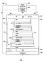
- FIG. 3there is shown a disk drive 300 embodying the present invention.
- at least one rotatable magnetic disk 312is supported on a spindle 314 and rotated by a disk drive motor 318 .
- the magnetic recording media on each diskis in the form of an annular pattern of concentric data tracks (not shown) on the disk 312 .
- At least one slider 313is positioned on the disk 312 , each slider 313 supporting one or more magnetic read/write heads 321 where the head 321 incorporates the dual MTJ sensor of the present invention.
- the slider 313is moved radially in and out over the disk surface 322 so that the heads 321 may access different portions of the disk where desired data are recorded.
- Each slider 313is attached to an actuator arm 319 by means of a suspension 315 .
- the suspension 315provides a slight spring force which biases the slider 313 against the disk surface 322 .
- Each actuator arm 319is attached to an actuator 327 .
- the actuator as shown in FIG. 3may be a voice coil motor (VCM).
- the VCMcomprises a coil movable within a fixed magnetic field, the direction and speed of the coil movements being controlled by the motor current signals supplied by a controller 329 .
- the rotation of the disk 312generates an air bearing between the slider 313 (the surface of the slider 313 which includes the head 321 and faces the surface of the disk 312 is referred to as an air bearing surface (ABS)) and the disk surface 322 which exerts an upward force or lift on the slider.
- ABSair bearing surface
- the air bearingthus counterbalances the slight spring force of the suspension 315 and supports the slider 313 off and slightly above the disk surface by a small, substantially constant spacing during normal operation.
- control signals generated by the control unit 329such as access control signals and internal clock signals.
- the control unit 329comprises logic control circuits, storage chips and a microprocessor.
- the control unit 329generates control signals to control various system operations such as drive motor control signals on line 323 and head position and seek control signals on line 328 .
- the control signals on line 328provide the desired current profiles to optimally move and position the slider 313 to the desired data track on the disk 312 .
- Read and write signalsare communicated to and from the read/write heads 321 by means of the recording channel 325 .
- Recording channel 325may be a partial response maximum likelihood (PMRL) channel or a peak detect channel.
- PMRLpartial response maximum likelihood
- the recording channel 325is a PMRL channel.
- disk storage systemsmay contain a large number of disks and actuator arms, and each actuator arm may support a number of sliders.
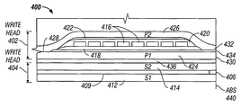
- FIG. 4is a side cross-sectional elevation view of a “piggyback” magnetic read/write head 400 , which includes a write head portion 402 and a read head portion 404 , the read head portion employing a dual MTJ sensor 406 according to the present invention.
- the MTJ sensor 406is sandwiched between ferromagnetic first and second shield layers 412 and 414 at the ABS 440 .
- a nonmagnetic insulating layer 409is sandwiched between the first and second shield layers 412 and 414 in the region behind the sensor extending away from the ABS to prevent shorting between the shield layers.
- the resistance of the SV sensor 406changes.
- a sense current I S conducted through the sensorcauses these resistance changes to be manifested as voltage changes. These voltage changes are then processed as readback signals by the processing circuitry of the data recording channel 325 shown in FIG. 3 .
- the write head portion 402 of the magnetic read/write head 400includes a coil layer 416 sandwiched between first and second insulation layers 418 and 420 .
- a third insulation layer 422may be employed for planarizing the head to eliminate ripples in the second insulation layer 420 caused by the coil layer 416 .
- the first, second and third insulation layersare referred to in the art as an insulation stack.
- the coil layer 416 and the first, second and third insulation layers 418 , 420 and 422are sandwiched between first and second pole piece layers 424 and 426 .
- the first and second pole piece layers 424 and 426are magnetically coupled at a back gap 428 and have first and second pole tips 430 and 432 which are separated by a write gap layer 434 at the ABS 440 .
- An insulation layer 436is located between the second shield layer 414 and the first pole piece layer 424 . Since the second shield layer 414 and the first pole piece layer 424 are separate layers this read/write head is known as a “piggyback”
- FIG. 5is the same as FIG. 4 except the second shield layer 414 and the first pole piece layer 424 are a common layer.
- This type of read/write headis known as a “merged” head 500 .
- the insulation layer 436 of the piggyback head in FIG. 4is omitted in the merged head 500 of FIG. 5 .
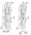
- FIG. 6shows an air bearing surface (ABS) view, not to scale, of a dual magnetic tunnel junction (MTJ) sensor 600 according to a preferred embodiment of the present invention.
- the MTJ sensor 600comprises end regions 604 and 606 separated from each other by a central region 602 .
- the seed layer 614is a layer deposited to modify the crystallographic texture or grain size of the subsequent layers, and may not be needed depending on the subsequent layer.
- a first MTJ stack 608 deposited over the seed layer 614comprises a first antiferromagnetic (AFM1) layer 616 , a first AP-pinned layer 617 , an electrically insulating tunnel barrier layer 624 and a first sense layer 625 .
- AFM1antiferromagnetic
- the first AP-pinned layer 617is formed of two ferromagnetic layers 618 and 622 separated by an antiparallel coupling (APC) layer 620 .
- the APC layeris formed of a nonmagnetic material, preferably ruthenium (Ru) that allows the two ferromagnetic layers 618 and 622 to be strongly antiparallel-coupled together.
- the AFM1 layer 616has a thickness at which the desired exchange properties are achieved, typically 100-300 ⁇ .
- a longitudinal bias stack 610 sequentially deposited over the first MTJ stack 608comprises a first decoupling layer 629 , a first ferromagnetic (FM1) layer 630 , a third antiferromagnetic (AFM3) layer 632 , a second ferromagnetic (FM2) layer 634 and a second decoupling layer 633 .
- a second MTJ stack 612 deposited over the longitudinal bias stack 610comprises a second sense layer 639 , a second tunnel barrier layer 640 , a second AP-pinned layer 641 and an antiferromagnetic (AFM2) layer 648 .
- the second AP-pinned layer 641is formed of two ferromagnetic layers 642 and 646 separated by an antiparallel coupling (APC) layer 644 .
- the APC layeris formed of a nonmagnetic material, preferably ruthenium (Ru) that allows the two ferromagnetic layers 642 and 646 to be strongly antiparallel-coupled together.
- the AFM2 layer 648has a thickness at which the desired exchange properties are achieved, typically 100-300 ⁇ .
- a cap layer 650formed on the AFM2 layer 648 , completes the central region 606 of the dual SV sensor 600 .
- the AFM1 layer 616is exchange-coupled to the first AP-pinned layer 617 to provide a pinning magnetic field to pin the magnetizations of the two ferromagnetic layers of the first AP-pinned layer perpendicular to the ABS as indicated by an arrow tail 619 and an arrow head 623 pointing into and out of the plane of the paper, respectively.
- the first sense layer 625has a magnetization 627 that is free to rotate in the presence of an external (signal) magnetic field.
- the magnetization 627 of the first sense layer 625is preferably oriented parallel to the ABS in the absence of an external magnetic field.
- the AFM2 layer 648is exchange-coupled to the second AP-pinned layer 641 to provide a pinning magnetic field to pin the magnetizations of the two ferromagnetic layers of the second AP-pinned layer perpendicular to the ABS as indicated by an arrow head 643 and an arrow tail 645 pointing out of and into the plane of the paper, respectively.
- the second sense layer 639has a magnetization 637 that is free to rotate in the presence of an external (signal) magnetic field.
- the magnetization 637 of the second sense layer 639is preferably oriented parallel to the ABS in the absence of an external magnetic field.
- the AFM3 layer 632is exchange-coupled to the FM1 layer 630 and the FM2 layer 634 to provide pinning fields to pin the magnetizations 631 and 635 , respectively, parallel to the plane of the ABS.
- the magnetizations 631 and 635provide longitudinal bias fields which form flux closures with the first and second sense layers 625 and 639 , respectively, to stabilize the first and second sense layers 625 and 639 .
- a signal detector 670which is electrically connected to the first and second shield layers 652 and 654 senses the change in resistance due to changes induced in the sense layers 625 and 639 by the external magnetic field (e.g., field generated by a data bit stored on a disk).
- the external fieldacts to rotate the magnetizations of the sense layers 625 and 639 relative to the magnetizations of the pinned layers 622 and 642 which are preferably pinned perpendicular to the ABS.
- the signal detector 670preferably comprises a partial response maximum likelihood (PRML) recording channel for processing the signal detected by MTJ sensor 600 .
- PRMLpartial response maximum likelihood
- a peak detect channel or a maximum likelihood channele.g., 1.7 ML
- the design and implementation of the aforementioned channelsare known to those skilled in the art.
- the signal detector 670also includes other supporting circuitries such as a preamplifier (electrically placed between the sensor and the channel) for conditioning the sensed resistance changes as is known to those skilled in the art.
- the MTJ sensor 600is fabricated in an integrated ion beam/DC magnetron sputtering system to sequentially deposit the multilayer structure shown in FIG. 6 .
- the sputter deposition processis carried out in the presence of a longitudinal magnetic field of about 40 Oe.
- the first shield layer 652 formed of Ni—Fe having a thickness of 10000 ⁇is deposited on a substrate 601 .
- the seed layer 614is a bilayer with a first sublayer of tantalum (Ta) having a thickness of 30 ⁇ and a second sublayer of Ni—Fe having a thickness of 10 ⁇ deposited on the first shield layer 652 .
- the first MTJ stack 608is formed on the seed layer by sequentially depositing the AFM1 layer 616 of Pt—Mn having a thickness of about 160 ⁇ , the ferromagnetic layer 618 of Co—Fe having a thickness of about 12 ⁇ , the APC layer 620 of ruthenium (Ru) having a thickness of about 8 ⁇ , the ferromagnetic layer 622 of Co—Fe having a thickness of about 18 ⁇ , the first tunnel barrier layer 624 of Al—O having a thickness of about 6 ⁇ , and the first sense layer 625 of Co—Fe having a thickness of about 18 ⁇ .
- the AFM1 layer 616 of Pt—Mnhaving a thickness of about 160 ⁇
- the ferromagnetic layer 618 of Co—Fehaving a thickness of about 12 ⁇
- the APC layer 620 of ruthenium (Ru)having a thickness of about 8 ⁇
- the ferromagnetic layer 622 of Co—Fehaving a thickness of about 18
- the tunnel barrier layer 624is formed by depositing and an aluminum (Al) film with DC-magnetron sputtering from a pure Al target in an argon gas of 3 mTorr, and then exposing to an oxygen gas of 2 Torr for 4 minutes. This optimum in situ oxidation is incorporated into this Al—O formation process for attaining a high tunneling magnetoresistance and low junction resistance.
- the longitudinal bias stack 610is formed on the first MTJ stack 608 by sequentially depositing the first decoupling layer 629 comprising a first sublayer 626 of Cu—O having a thickness of about 10 ⁇ and a second sublayer 628 of ruthenium (Ru) having a thickness of about 20 ⁇ , the FM1 layer 630 of Co—Fe having a thickness of about 24 ⁇ , the AFM3 layer 632 of Ir—Mn having a thickness of about 60 ⁇ , the FM2 layer 634 of Co—Fe having a thickness of about 24 ⁇ , and the second decoupling layer 636 comprising a first sublayer 636 of ruthenium (Ru) having a thickness of about 20 ⁇ and a second sublayer 638 of Cu—O having a thickness of about 10 ⁇ .
- the first decoupling layer 629comprising a first sublayer 626 of Cu—O having a thickness of about 10 ⁇ and a second sublayer 628 of ruthenium (Ru) having a thickness of about
- the Cu—O sublayers 626 and 638are formed by depositing a copper (Cu) film with DC-magnetron sputtering from a pure Cu target in a mixture of argon and oxygen gases of 2.985 and 0.015 mTorr, respectively, and then exposing to a mixture of argon and oxygen gases of 2.94 and 0.06 mTorr, respectively, for 4 minutes.
- the Cu—O filmsfacilitate the sense layers to exhibit good soft magnetic properties.
- the second MTJ stack 612is formed on the longitudinal bias stack 610 by sequentially depositing the second sense layer 639 of Co—Fe having a thickness of about 18 ⁇ , the second tunnel barrier layer 640 of Al—O having a thickness of about 6 ⁇ , the ferromagnetic layer 642 of Co—Fe having a thickness of about 18 ⁇ , the APC layer 644 of ruthenium (Ru) having a thickness of about 8 ⁇ , the ferromagnetic layer 646 of Co—Fe having a thickness of about 12 ⁇ , and the AFM2 layer 648 of Pt—Mn having a thickness of about 160 ⁇ .
- the second sense layer 639 of Co—Fehaving a thickness of about 18 ⁇
- the second tunnel barrier layer 640 of Al—Ohaving a thickness of about 6 ⁇
- the ferromagnetic layer 642 of Co—Fehaving a thickness of about 18 ⁇
- the APC layer 644 of ruthenium (Ru)having a thickness of about 8 ⁇
- the tunnel barrier layer 640is formed by depositing and an aluminum (Al) film with DC-magnetron sputtering from a pure Al target in an argon gas of 3 mTorr, and then exposing to an oxygen gas of 2 Torr for 4 minutes. This optimum in situ oxidation is incorporated into this Al—O formation process for attaining a high tunneling magnetoresistance and low junction resistance.
- the cap layer 650is a bilayer with a first sublayer of ruthenium (Ru) having a thickness of 40 ⁇ and a second sublayer of tantalum (Ta) having a thickness of 30 ⁇ formed over the AFM2 layer 648 .
- the second shield layer 654 formed of Ni—Fe having a thickness of 10000 ⁇is deposited over the cap layer 650 .
- An insulating layer 656 formed of Al 2 O 3 deposited between the first shield layer 652 and the second shield layer 654provides electrical insulation between the shields/leads and prevents shunting of the sense current around the active region 602 of the dual MTJ sensor 600 .
- the senoris annealed for 2 hours at 280° C. in the presence of a magnetic field of about 10,000 Oe in a transverse direction perpendicular to the ABS and is then cooled while still in the magnetic field to set the exchange coupling of the AFM1 and AFM2 layers 616 and 648 with the AP-pinned layers 617 and 641 , respectively, so that the magnetizations in the two AP-pinned layers are perpendicular to the ABS with net magnetic moments canceling each other. This results in cancellation of the demagnetization fields between the AP-pinned layers 617 and 641 .
- a second annealis carried out for 2 hours at 240° C. in the presence of a magnetic field of 200 Oe in a longitudinal direction parallel to the ABS. Because the blocking temperature of the Pt—Mn antiferromagnetic material (>360° C.) of the AFM1 and AFM2 layers is higher than 240° C., the magnetizations of the first and second AP-pinned layers 617 and 641 are not rotated while the magnetizations 631 and 635 in the longitudinal bias stack are oriented in the longitudinal direction due to the lower (less than 240° C.) blocking temperature of the Ir—Mn antiferromagnetic material of the AFM3 layer.
- the magnetization 631 of the FM1 layer 630forms a flux closure with the magnetization 627 of the first sense layer 625 providing stability for the first sense layer 625 .
- the magnetization 635 of the FM2 layer 634forms a flux closure with the magnetization 637 of the second sense layer 639 providing stability of the second sense layer 639 .
- the Cu—O/Ru and Ru/Cu—O filmsare used as first and second decoupling layers 629 and 633 .
- Either one of the Cu—O or Ru filmsare not used alone as a decoupling layer since strong exchange coupling occurs across either film and full decoupling can only be attained when the film thickness is far greater than 30 ⁇ .
- the decoupling layer thicknessis preferred to be as small as possible, but not to be too small to induce the echange coupling.
- the Cu—O film of the decoupling layersis adjacent to the Co—Fe sense layers to promote good soft magnetic properties.
- the Ru film of the decoupling layersis also used as a seed layer for the Co—Fe/Ir—Mn/Co—Fe longitudinal bias layers to promote high unidirectional anisotropy fields (H UA ).
- the Co—Fe/Ir—Mn/Co—Fe film stackis used for antiferromagnetic stabilization of the dual MTJ sensors.
- a Ni—Fe(10 ⁇ ) /Co—Pt(40 ⁇ ) /Ni—Fe(10 ⁇ ) film stackcan be used to replace the Co—Fe/Ir—Mn/Co—Fe film stack for hard magnetic stabilization.
- the Ni—Fe filmis adjacent to the Co—Pt film in order to reduce stray fields from the Co—Pt film and improve its squareness.
- the longitudinal field anneal used to longitudinally orient the magnetizations of the Co—Fe/Ir—Mn/Co—Fe stackis eliminated, but magnetic setting of the Ni—fe/Co—Pt/Ni—Fe stack in a field of 3 kOe must be conducted at room temperature after the head fabrication process.
- FIG. 7shows an air bearing surface (ABS) view, not to scale, of a dual magnetic tunnel junction (MTJ) sensor 700 according to another embodiment of the present invention.
- the dual MTJ sensor 700is the same as the dual MTJ sensor 600 shown in FIG. 6 except that in order to achieve a read gap thickness of 50 nm the AFM1 and AFM2 layers 616 and 648 have been eliminated and the AFM3 layer 632 of the longitudinal bias stack 610 has been replaced by an AFM3 layer 716 of Pt—Mn having a thickness of 160 ⁇ .
- the MTJ sensor 700comprises a first MTJ stack 708 , a second MTJ stack 712 and a longitudinal bias stack 710 disposed between the first and second MTJ stacks 708 and 712 .
- the first MTJ stack 708is the same as MTJ stack 608 without the AFM1 layer 616 and the second MTJ stack 712 is the same as MTJ stack 612 without the AFM2 layer 648 .
- the longitudinal bias stack 710is the same as bias stack 610 with the AFM3 layer of Ir—replaced with an AFM3 layer 716 of Pt—Mn having a thickness of 160 ⁇ .
- the MTJ sensor 700is fabricated in an integrated ion beam/DC magnetron sputtering system to sequentially deposit the multilayer structure shown in FIG. 7 .
- the deposition processis the same as the process used to fabricate the MTJ sensor 600 .
- the MTJ sensor 700is annealed for 2 hours at 280° C. in the presence of a magnetic field of 200 Oe in a longitudinal direction parallel to the ABS.
- the magnetic fieldis higher than the uniaxial anisotropy field H K ( ⁇ 20 Oe) of the as-deposited Co—Fe/Pt—Mn/Co—Fe films so that strong exchange coupling in the Co—Fe/Pt—Mn/Co—Fe films can be developed in a longitudinal direction parallel to the ABS during annealing.
- the magnetic fieldis less than the spin flop field H SF ( ⁇ 1 koe) of the first and second pinned layers 617 and 641 so that strong antiparallel coupling across the Ru APC layers in the first and second AP-pinned layers 617 and 641 is not interrupted during annealing.
- the transverse pinningcan still be attained due to a strong spin-flop field (H SP ) induced from antiparallel coupling across the Ru APC layers.
- H SPspin-flop field
- the transverse pinningcan be further reinforced if the Co—Fe films adjacent to the Ru APC layers have a high intrinsic uniaxial anisotropy field (H K ) and a high positive saturation magnetostriction ( ⁇ S ).
- the Co 90 —Fe 10 (in atomic %) commonly used for the ferromagnetic layers of the AP-pinned layers 617 and 641has an H K of 16 Oe.
- H Kbecomes 30 Oe and the ⁇ S increases to 35.1 ⁇ 10 ⁇ 6 (corresponding to 142 Oe).
- a Co—Fe film with an Fe content of 20 at. % or higher (up to 50 at. %)is preferably used for the ferromagnetic layers of the AP-pinned layers.
- H K +H K ′(172.5 Oe) is not as high as H UA (600 Oe) and H SP (900 Oe), it has two major unique features, leading it to play an important role in providing transverse pinning.
- H K +H K ′is determined only from the Co—Fe film itself, while H UA and H SP are determined not only from the Co—Fe film, but also from its adjacent Ru and Pt—Mn films.
- the temperature dependence of H K +H K ′is determined by the Curie temperature of the Co—Fe film ( ⁇ 700° C.), while the temperature dependence of H UA is determined by the blocking temperature of the exchange-coupled Pt—Mn/Co—Fe films ( ⁇ 360° C.), and the temperature dependence of H SP is determined by the critical temperature of the antiparallel-coupled Co—Fe/Ru/Co—Fe films. Since the Curie temperature is much higher than the blocking and critical temperatures, H K +H K ′ can remain nearly unchanged at elevated sensor operation temperatures ( ⁇ 180° C.). Thus H K +H K ′ may play a crucial role in improving thermal stability.
- H K +H K ′substantially reduces edge curling effects of magnetizations of the ferromagnetic AP-pinned layers.
- the reduction in the edge curling effectsresults in more uniform magnetization along the sensor height, therefore providing better flux closure to cancel magnetization more efficiently.
- the transverse pinning field resulting from H SP , H K and H K ′should be high enough for proper sensor operation.
Landscapes
- Engineering & Computer Science (AREA)
- Physics & Mathematics (AREA)
- Manufacturing & Machinery (AREA)
- Chemical & Material Sciences (AREA)
- Nanotechnology (AREA)
- Condensed Matter Physics & Semiconductors (AREA)
- General Physics & Mathematics (AREA)
- Crystallography & Structural Chemistry (AREA)
- Mathematical Physics (AREA)
- Theoretical Computer Science (AREA)
- Hall/Mr Elements (AREA)
- Magnetic Heads (AREA)
Abstract
Description
Claims (14)
Priority Applications (1)
| Application Number | Priority Date | Filing Date | Title |
|---|---|---|---|
| US10/981,926US8133363B2 (en) | 2002-04-02 | 2004-11-05 | Dual magnetic tunnel junction sensor with a longitudinal bias stack |
Applications Claiming Priority (2)
| Application Number | Priority Date | Filing Date | Title |
|---|---|---|---|
| US10/116,017US6822838B2 (en) | 2002-04-02 | 2002-04-02 | Dual magnetic tunnel junction sensor with a longitudinal bias stack |
| US10/981,926US8133363B2 (en) | 2002-04-02 | 2004-11-05 | Dual magnetic tunnel junction sensor with a longitudinal bias stack |
Related Parent Applications (1)
| Application Number | Title | Priority Date | Filing Date |
|---|---|---|---|
| US10/116,017DivisionUS6822838B2 (en) | 2002-04-02 | 2002-04-02 | Dual magnetic tunnel junction sensor with a longitudinal bias stack |
Publications (2)
| Publication Number | Publication Date |
|---|---|
| US20050061658A1 US20050061658A1 (en) | 2005-03-24 |
| US8133363B2true US8133363B2 (en) | 2012-03-13 |
Family
ID=28453927
Family Applications (2)
| Application Number | Title | Priority Date | Filing Date |
|---|---|---|---|
| US10/116,017Expired - LifetimeUS6822838B2 (en) | 2002-04-02 | 2002-04-02 | Dual magnetic tunnel junction sensor with a longitudinal bias stack |
| US10/981,926Expired - Fee RelatedUS8133363B2 (en) | 2002-04-02 | 2004-11-05 | Dual magnetic tunnel junction sensor with a longitudinal bias stack |
Family Applications Before (1)
| Application Number | Title | Priority Date | Filing Date |
|---|---|---|---|
| US10/116,017Expired - LifetimeUS6822838B2 (en) | 2002-04-02 | 2002-04-02 | Dual magnetic tunnel junction sensor with a longitudinal bias stack |
Country Status (1)
| Country | Link |
|---|---|
| US (2) | US6822838B2 (en) |
Cited By (3)
| Publication number | Priority date | Publication date | Assignee | Title |
|---|---|---|---|---|
| US20120225322A1 (en)* | 2009-09-07 | 2012-09-06 | Agency For Science Technology And Research | Sensor Arrangement |
| US9230578B2 (en) | 2013-12-23 | 2016-01-05 | HGST Netherlands B.V. | Multiple readers for high resolution and SNR for high areal density application |
| US11980039B2 (en) | 2021-06-16 | 2024-05-07 | International Business Machines Corporation | Wide-base magnetic tunnel junction device with sidewall polymer spacer |
Families Citing this family (45)
| Publication number | Priority date | Publication date | Assignee | Title |
|---|---|---|---|---|
| US6847509B2 (en)* | 2001-02-01 | 2005-01-25 | Kabushiki Kaisha Toshiba | Magnetoresistive head and perpendicular magnetic recording-reproducing apparatus |
| KR100407907B1 (en)* | 2001-05-15 | 2003-12-03 | 한국과학기술연구원 | Thermal anneal method of magnetic tunnel junction, and magnetic tunneling junction fabricated by the method |
| JP3793725B2 (en)* | 2002-01-25 | 2006-07-05 | アルプス電気株式会社 | Magnetic detection element, method of manufacturing the same, and magnetic detection apparatus using the magnetic detection element |
| US7370404B2 (en)* | 2002-03-21 | 2008-05-13 | Hitachi Global Storage Technologies Netherlands B.V. | Method for resetting pinned layer magnetization in a magnetoresistive sensor |
| US7161771B2 (en)* | 2002-04-02 | 2007-01-09 | Hitachi Global Storage Technologies Netherlands B.V. | Dual spin valve sensor with a longitudinal bias stack |
| DE10214946B4 (en)* | 2002-04-04 | 2006-01-19 | "Stiftung Caesar" (Center Of Advanced European Studies And Research) | TMR sensor |
| US7196882B2 (en)* | 2002-07-23 | 2007-03-27 | Micron Technology, Inc. | Magnetic tunnel junction device and its method of fabrication |
| US7224556B2 (en)* | 2002-10-24 | 2007-05-29 | Hitachi Global Storage Technologies Netherlands B.V. | Self-pinned CPP magnetoresistive sensor |
| JP3961497B2 (en)* | 2003-04-18 | 2007-08-22 | アルプス電気株式会社 | CPP type giant magnetoresistive head |
| JP2005086112A (en)* | 2003-09-10 | 2005-03-31 | Toshiba Corp | Magnetoresistive element, magnetic head, head suspension assembly, and magnetic reproducing apparatus |
| US7230802B2 (en)* | 2003-11-12 | 2007-06-12 | Hitachi Global Storage Technologies Netherlands B.V. | Method and apparatus for providing magnetostriction control in a freelayer of a magnetic memory device |
| EP1697585A4 (en)* | 2003-12-15 | 2009-04-08 | Univ Yale | MAGNETOELECTRONIC DEVICES BASED ON COLOSSAL MAGNETOESISTANT THIN FILMS |
| US7233461B2 (en)* | 2004-01-20 | 2007-06-19 | Hitachi Global Storage Technologies Netherlands, B.V. | Stabilization structure for CPP GMR/TV |
| US7283333B2 (en)* | 2004-02-11 | 2007-10-16 | Hitachi Global Storage Technologies Netherlands B.V. | Self-pinned double tunnel junction head |
| US7320169B2 (en)* | 2004-05-14 | 2008-01-22 | Headway Technologies, Inc. | Self-pinned GMR structure by annealing |
| US7511926B2 (en)* | 2004-06-14 | 2009-03-31 | Hitachi Global Storage Technologies Netherlands B.V. | Larger dR CPP GMR structure |
| JP4690675B2 (en)* | 2004-07-30 | 2011-06-01 | 株式会社東芝 | Magnetoresistive element, magnetic head, and magnetic recording / reproducing apparatus |
| US7436636B2 (en)* | 2004-11-10 | 2008-10-14 | Hitachi Global Storage Technologies Netherlands B.V. | Dual CPP GMR sensor with in-stack bias structure |
| US7408747B2 (en)* | 2005-02-01 | 2008-08-05 | Hitachi Global Storage Technologies Netherlands B.V. | Enhanced anti-parallel-pinned sensor using thin ruthenium spacer and high magnetic field annealing |
| US7612970B2 (en)* | 2005-02-23 | 2009-11-03 | Hitachi Global Storage Technologies Netherlands B.V. | Magnetoresistive sensor with a free layer stabilized by direct coupling to in stack antiferromagnetic layer |
| US7285836B2 (en)* | 2005-03-09 | 2007-10-23 | Maglabs, Inc. | Magnetic random access memory with stacked memory cells having oppositely-directed hard-axis biasing |
| JP4521316B2 (en)* | 2005-05-26 | 2010-08-11 | 株式会社東芝 | Magnetoresistive element, magnetic head, and magnetic recording / reproducing apparatus |
| US7652856B2 (en)* | 2005-12-27 | 2010-01-26 | Hitachi Global Storage Technologies Netherlands B.V. | Current perpendicular to plane (CPP) magnetoresistive sensor having strong pinning and small gap thickness |
| US20070153432A1 (en)* | 2005-12-29 | 2007-07-05 | Tdk Corporation | Magnetic head |
| JP4764294B2 (en)* | 2006-09-08 | 2011-08-31 | 株式会社東芝 | Magnetoresistive element and magnetic head |
| KR100834811B1 (en) | 2006-11-28 | 2008-06-09 | 고려대학교 산학협력단 | Cobalt-Iron-Silicon-Boron / Platinum Multilayer Thin Film with Vertical Magnetic Anisotropy |
| CN101473372A (en)* | 2007-03-20 | 2009-07-01 | 富士通株式会社 | Magnetic head |
| JP4768066B2 (en)* | 2007-03-20 | 2011-09-07 | アルプス電気株式会社 | Position detecting device using magnetoresistive effect element |
| US7742328B2 (en)* | 2007-06-15 | 2010-06-22 | Grandis, Inc. | Method and system for providing spin transfer tunneling magnetic memories utilizing non-planar transistors |
| US20110026169A1 (en)* | 2009-07-28 | 2011-02-03 | Hardayal Singh Gill | Dual cpp gmr head using a scissor sensor |
| US8503135B2 (en)* | 2011-09-21 | 2013-08-06 | Seagate Technology Llc | Magnetic sensor with enhanced magnetoresistance ratio |
| KR20130034260A (en)* | 2011-09-28 | 2013-04-05 | 에스케이하이닉스 주식회사 | Method for fabricating semiconductor device |
| US8685756B2 (en) | 2011-09-30 | 2014-04-01 | Everspin Technologies, Inc. | Method for manufacturing and magnetic devices having double tunnel barriers |
| EP2597692A1 (en)* | 2011-11-22 | 2013-05-29 | Crocus Technology S.A. | Self-referenced MRAM cell with optimized reliability |
| US9082435B1 (en) | 2014-01-15 | 2015-07-14 | HGST Netherlands, B.V. | Fabrication of multiple sensor layers with self-aligned back edge |
| JP6455804B2 (en)* | 2014-02-12 | 2019-01-23 | Tdk株式会社 | Magnetic element |
| JP6978000B2 (en)* | 2016-02-19 | 2021-12-08 | 国立大学法人東北大学 | Manufacturing method of tunnel magnetoresistive element |
| US10790441B2 (en) | 2016-03-14 | 2020-09-29 | Purdue Research Foundation | Spin-transfer-torque synthetic anti-ferromagnetic switching device |
| JP7359696B2 (en)* | 2017-04-07 | 2023-10-11 | クロッカス・テクノロジー・ソシエテ・アノニム | Magnetic sensor cell for measuring one-dimensional and two-dimensional magnetic fields and method for measuring magnetic fields using the magnetic sensor cell |
| EP3385741B1 (en)* | 2017-04-07 | 2019-12-18 | Crocus Technology S.A. | Magnetic sensor cell for measuring one- and two-dimensional magnetic fields and method for measuring said magnetic fields using the magnetic sensor cell |
| EP3673522B1 (en) | 2017-08-23 | 2022-10-05 | Everspin Technologies, Inc. | Magnetoresistive bit fabrication by multi-step etching |
| US11171283B2 (en)* | 2019-11-01 | 2021-11-09 | International Business Machines Corporation | Modified double magnetic tunnel junction structure suitable for BEOL integration |
| US11316104B2 (en) | 2020-03-13 | 2022-04-26 | International Business Machines Corporation | Inverted wide base double magnetic tunnel junction device |
| US12063868B2 (en) | 2021-03-17 | 2024-08-13 | International Business Machines Corporation | Low RA narrow base modified double magnetic tunnel junction structure |
| US11501810B2 (en)* | 2021-03-17 | 2022-11-15 | International Business Machines Corporation | Amorphous spin diffusion layer for modified double magnetic tunnel junction structure |
Citations (20)
| Publication number | Priority date | Publication date | Assignee | Title |
|---|---|---|---|---|
| US5287238A (en) | 1992-11-06 | 1994-02-15 | International Business Machines Corporation | Dual spin valve magnetoresistive sensor |
| US5442508A (en) | 1994-05-25 | 1995-08-15 | Eastman Kodak Company | Giant magnetoresistive reproduce head having dual magnetoresistive sensor |
| US5576915A (en) | 1993-03-15 | 1996-11-19 | Kabushiki Kaisha Toshiba | Magnetoresistive head with antiferromagnetic sublayers interposed between first and second spin-valve units to exchange bias inner magnetic films thereof |
| US5635835A (en)* | 1994-07-21 | 1997-06-03 | Commissariat A L'energie Atomique | Self biased multilayer magnetoresistance sensor |
| US5701222A (en) | 1995-09-11 | 1997-12-23 | International Business Machines Corporation | Spin valve sensor with antiparallel magnetization of pinned layers |
| US5705973A (en) | 1996-08-26 | 1998-01-06 | Read-Rite Corporation | Bias-free symmetric dual spin valve giant magnetoresistance transducer |
| US5757056A (en) | 1996-11-12 | 1998-05-26 | University Of Delaware | Multiple magnetic tunnel structures |
| US5856897A (en) | 1996-11-27 | 1999-01-05 | International Business Machines Corporation | Self-biased dual spin valve sensor |
| US5859754A (en) | 1997-04-03 | 1999-01-12 | Read-Rite Corporation | Magnetoresistive transducer having a common magnetic bias using assertive and complementary signals |
| US5869963A (en) | 1996-09-12 | 1999-02-09 | Alps Electric Co., Ltd. | Magnetoresistive sensor and head |
| US6023395A (en) | 1998-05-29 | 2000-02-08 | International Business Machines Corporation | Magnetic tunnel junction magnetoresistive sensor with in-stack biasing |
| US6069820A (en) | 1998-02-20 | 2000-05-30 | Kabushiki Kaisha Toshiba | Spin dependent conduction device |
| US6114719A (en) | 1998-05-29 | 2000-09-05 | International Business Machines Corporation | Magnetic tunnel junction memory cell with in-stack biasing of the free ferromagnetic layer and memory array using the cell |
| US6185078B1 (en) | 1998-08-21 | 2001-02-06 | International Business Machines Corporation | Spin valve read head with antiferromagnetic oxide film as longitudinal bias layer and portion of first read gap |
| US6275363B1 (en)* | 1999-07-23 | 2001-08-14 | International Business Machines Corporation | Read head with dual tunnel junction sensor |
| US6341053B1 (en)* | 1997-10-30 | 2002-01-22 | Nec Corporation | Magnetic tunnel junction elements and their fabrication method |
| US6381105B1 (en)* | 1999-10-22 | 2002-04-30 | Read-Rite Corporation | Hybrid dual spin valve sensor and method for making same |
| US6392849B2 (en)* | 1997-04-25 | 2002-05-21 | Hitachi, Ltd. | Magnetic head with dual spin valve element for differential operation |
| US6590803B2 (en)* | 2001-03-27 | 2003-07-08 | Kabushiki Kaisha Toshiba | Magnetic memory device |
| US7413636B2 (en)* | 2002-04-02 | 2008-08-19 | Hitachi Global Storage Technologies Netherlands B. V. | Method for manufacturing a dual spin valve sensor having a longitudinal bias stack |
Family Cites Families (6)
| Publication number | Priority date | Publication date | Assignee | Title |
|---|---|---|---|---|
| US6185079B1 (en)* | 1998-11-09 | 2001-02-06 | International Business Machines Corporation | Disk drive with thermal asperity reduction circuitry using a magnetic tunnel junction sensor |
| US6178074B1 (en)* | 1998-11-19 | 2001-01-23 | International Business Machines Corporation | Double tunnel junction with magnetoresistance enhancement layer |
| US6259586B1 (en)* | 1999-09-02 | 2001-07-10 | International Business Machines Corporation | Magnetic tunnel junction sensor with AP-coupled free layer |
| US6556390B1 (en)* | 1999-10-28 | 2003-04-29 | Seagate Technology Llc | Spin valve sensors with an oxide layer utilizing electron specular scattering effect |
| US6633461B2 (en)* | 2001-03-20 | 2003-10-14 | Hitachi Global Storage Technologies Netherlands B.V. | Dual tunnel junction sensor antiferromagnetic layer between pinned layers |
| US6680832B2 (en)* | 2001-05-11 | 2004-01-20 | International Business Machines Corporation | CPP magnetoresistive sensors with in-stack longitudinal biasing and overlapping magnetic shield |
- 2002
- 2002-04-02USUS10/116,017patent/US6822838B2/ennot_activeExpired - Lifetime
- 2004
- 2004-11-05USUS10/981,926patent/US8133363B2/ennot_activeExpired - Fee Related
Patent Citations (21)
| Publication number | Priority date | Publication date | Assignee | Title |
|---|---|---|---|---|
| US5287238A (en) | 1992-11-06 | 1994-02-15 | International Business Machines Corporation | Dual spin valve magnetoresistive sensor |
| US5768066A (en) | 1993-03-15 | 1998-06-16 | Kabushiki Kaisha Toshiba | Magnetoresistive head having an antiferromagnetic layer interposed between first and second magnetoresistive elements |
| US5576915A (en) | 1993-03-15 | 1996-11-19 | Kabushiki Kaisha Toshiba | Magnetoresistive head with antiferromagnetic sublayers interposed between first and second spin-valve units to exchange bias inner magnetic films thereof |
| US5442508A (en) | 1994-05-25 | 1995-08-15 | Eastman Kodak Company | Giant magnetoresistive reproduce head having dual magnetoresistive sensor |
| US5635835A (en)* | 1994-07-21 | 1997-06-03 | Commissariat A L'energie Atomique | Self biased multilayer magnetoresistance sensor |
| US5701222A (en) | 1995-09-11 | 1997-12-23 | International Business Machines Corporation | Spin valve sensor with antiparallel magnetization of pinned layers |
| US5705973A (en) | 1996-08-26 | 1998-01-06 | Read-Rite Corporation | Bias-free symmetric dual spin valve giant magnetoresistance transducer |
| US5869963A (en) | 1996-09-12 | 1999-02-09 | Alps Electric Co., Ltd. | Magnetoresistive sensor and head |
| US5757056A (en) | 1996-11-12 | 1998-05-26 | University Of Delaware | Multiple magnetic tunnel structures |
| US5856897A (en) | 1996-11-27 | 1999-01-05 | International Business Machines Corporation | Self-biased dual spin valve sensor |
| US5859754A (en) | 1997-04-03 | 1999-01-12 | Read-Rite Corporation | Magnetoresistive transducer having a common magnetic bias using assertive and complementary signals |
| US6392849B2 (en)* | 1997-04-25 | 2002-05-21 | Hitachi, Ltd. | Magnetic head with dual spin valve element for differential operation |
| US6341053B1 (en)* | 1997-10-30 | 2002-01-22 | Nec Corporation | Magnetic tunnel junction elements and their fabrication method |
| US6069820A (en) | 1998-02-20 | 2000-05-30 | Kabushiki Kaisha Toshiba | Spin dependent conduction device |
| US6023395A (en) | 1998-05-29 | 2000-02-08 | International Business Machines Corporation | Magnetic tunnel junction magnetoresistive sensor with in-stack biasing |
| US6114719A (en) | 1998-05-29 | 2000-09-05 | International Business Machines Corporation | Magnetic tunnel junction memory cell with in-stack biasing of the free ferromagnetic layer and memory array using the cell |
| US6185078B1 (en) | 1998-08-21 | 2001-02-06 | International Business Machines Corporation | Spin valve read head with antiferromagnetic oxide film as longitudinal bias layer and portion of first read gap |
| US6275363B1 (en)* | 1999-07-23 | 2001-08-14 | International Business Machines Corporation | Read head with dual tunnel junction sensor |
| US6381105B1 (en)* | 1999-10-22 | 2002-04-30 | Read-Rite Corporation | Hybrid dual spin valve sensor and method for making same |
| US6590803B2 (en)* | 2001-03-27 | 2003-07-08 | Kabushiki Kaisha Toshiba | Magnetic memory device |
| US7413636B2 (en)* | 2002-04-02 | 2008-08-19 | Hitachi Global Storage Technologies Netherlands B. V. | Method for manufacturing a dual spin valve sensor having a longitudinal bias stack |
Cited By (4)
| Publication number | Priority date | Publication date | Assignee | Title |
|---|---|---|---|---|
| US20120225322A1 (en)* | 2009-09-07 | 2012-09-06 | Agency For Science Technology And Research | Sensor Arrangement |
| US8659853B2 (en)* | 2009-09-07 | 2014-02-25 | Agency For Science, Technology And Research | Sensor arrangement |
| US9230578B2 (en) | 2013-12-23 | 2016-01-05 | HGST Netherlands B.V. | Multiple readers for high resolution and SNR for high areal density application |
| US11980039B2 (en) | 2021-06-16 | 2024-05-07 | International Business Machines Corporation | Wide-base magnetic tunnel junction device with sidewall polymer spacer |
Also Published As
| Publication number | Publication date |
|---|---|
| US20050061658A1 (en) | 2005-03-24 |
| US20030184919A1 (en) | 2003-10-02 |
| US6822838B2 (en) | 2004-11-23 |
Similar Documents
| Publication | Publication Date | Title |
|---|---|---|
| US8133363B2 (en) | Dual magnetic tunnel junction sensor with a longitudinal bias stack | |
| US7413636B2 (en) | Method for manufacturing a dual spin valve sensor having a longitudinal bias stack | |
| US6947264B2 (en) | Self-pinned in-stack bias structure for magnetoresistive read heads | |
| US6600638B2 (en) | Corrosion resistive GMR and MTJ sensors | |
| US7283333B2 (en) | Self-pinned double tunnel junction head | |
| US6473275B1 (en) | Dual hybrid magnetic tunnel junction/giant magnetoresistive sensor | |
| US6667861B2 (en) | Dual/differential GMR head with a single AFM layer | |
| US6052263A (en) | Low moment/high coercivity pinned layer for magnetic tunnel junction sensors | |
| US6127045A (en) | Magnetic tunnel junction device with optimized ferromagnetic layer | |
| US6538859B1 (en) | Giant magnetoresistive sensor with an AP-coupled low Hk free layer | |
| US6097579A (en) | Tunnel junction head structure without current shunting | |
| US6219212B1 (en) | Magnetic tunnel junction head structure with insulating antiferromagnetic layer | |
| US20030235016A1 (en) | Stabilization structures for CPP sensor | |
| US7505235B2 (en) | Method and apparatus for providing magnetostriction control in a freelayer of a magnetic memory device | |
| US8474127B2 (en) | Method for enhancing thermal stability, improving biasing and reducing damage from electrostatic discharge in self-pinned abutted junction heads | |
| US6600184B1 (en) | System and method for improving magnetic tunnel junction sensor magnetoresistance | |
| US6927948B2 (en) | Differential CPP GMR sensor with free layers separated by metal gap layer | |
| US7092220B2 (en) | Apparatus for enhancing thermal stability, improving biasing and reducing damage from electrostatic discharge in self-pinned abutted junction heads having a first self-pinned layer extending under the hard bias layers | |
| US6788502B1 (en) | Co-Fe supermalloy free layer for magnetic tunnel junction heads | |
| US6724586B2 (en) | Bias structure for magnetic tunnel junction magnetoresistive sensor | |
| US7072154B2 (en) | Method and apparatus for providing a self-pinned bias layer that extends beyond the ends of the free layer | |
| US7360297B2 (en) | Magnetoresistive sensor with antiparallel coupled lead/sensor overlap region | |
| US7050277B2 (en) | Apparatus having a self-pinned abutted junction magnetic read sensor with hard bias layers formed over ends of a self-pinned layer and extending under a hard bias layer | |
| JP2001307308A (en) | Magnetoresistive head and information reproducing apparatus | |
| US7570462B2 (en) | Read sensor with a uniform longitudinal bias stack |
Legal Events
| Date | Code | Title | Description |
|---|---|---|---|
| STCF | Information on status: patent grant | Free format text:PATENTED CASE | |
| CC | Certificate of correction | ||
| AS | Assignment | Owner name:GLOBALFOUNDRIES U.S. 2 LLC, NEW YORK Free format text:ASSIGNMENT OF ASSIGNORS INTEREST;ASSIGNOR:INTERNATIONAL BUSINESS MACHINES CORPORATION;REEL/FRAME:036550/0001 Effective date:20150629 | |
| FPAY | Fee payment | Year of fee payment:4 | |
| AS | Assignment | Owner name:GLOBALFOUNDRIES INC., CAYMAN ISLANDS Free format text:ASSIGNMENT OF ASSIGNORS INTEREST;ASSIGNORS:GLOBALFOUNDRIES U.S. 2 LLC;GLOBALFOUNDRIES U.S. INC.;REEL/FRAME:036779/0001 Effective date:20150910 | |
| AS | Assignment | Owner name:WILMINGTON TRUST, NATIONAL ASSOCIATION, DELAWARE Free format text:SECURITY AGREEMENT;ASSIGNOR:GLOBALFOUNDRIES INC.;REEL/FRAME:049490/0001 Effective date:20181127 | |
| FEPP | Fee payment procedure | Free format text:MAINTENANCE FEE REMINDER MAILED (ORIGINAL EVENT CODE: REM.); ENTITY STATUS OF PATENT OWNER: LARGE ENTITY | |
| LAPS | Lapse for failure to pay maintenance fees | Free format text:PATENT EXPIRED FOR FAILURE TO PAY MAINTENANCE FEES (ORIGINAL EVENT CODE: EXP.); ENTITY STATUS OF PATENT OWNER: LARGE ENTITY | |
| STCH | Information on status: patent discontinuation | Free format text:PATENT EXPIRED DUE TO NONPAYMENT OF MAINTENANCE FEES UNDER 37 CFR 1.362 | |
| FP | Lapsed due to failure to pay maintenance fee | Effective date:20200313 | |
| AS | Assignment | Owner name:GLOBALFOUNDRIES INC., CAYMAN ISLANDS Free format text:RELEASE BY SECURED PARTY;ASSIGNOR:WILMINGTON TRUST, NATIONAL ASSOCIATION;REEL/FRAME:054636/0001 Effective date:20201117 | |
| AS | Assignment | Owner name:GLOBALFOUNDRIES U.S. INC., NEW YORK Free format text:RELEASE BY SECURED PARTY;ASSIGNOR:WILMINGTON TRUST, NATIONAL ASSOCIATION;REEL/FRAME:056987/0001 Effective date:20201117 |