US8129778B2 - Semiconductor devices and methods for making the same - Google Patents
Semiconductor devices and methods for making the sameDownload PDFInfo
- Publication number
- US8129778B2 US8129778B2US12/629,232US62923209AUS8129778B2US 8129778 B2US8129778 B2US 8129778B2US 62923209 AUS62923209 AUS 62923209AUS 8129778 B2US8129778 B2US 8129778B2
- Authority
- US
- United States
- Prior art keywords
- dopant
- trench
- epitaxial layer
- conductivity type
- substrate
- Prior art date
- Legal status (The legal status is an assumption and is not a legal conclusion. Google has not performed a legal analysis and makes no representation as to the accuracy of the status listed.)
- Active, expires
Links
Images


Classifications
- H—ELECTRICITY
- H10—SEMICONDUCTOR DEVICES; ELECTRIC SOLID-STATE DEVICES NOT OTHERWISE PROVIDED FOR
- H10D—INORGANIC ELECTRIC SEMICONDUCTOR DEVICES
- H10D30/00—Field-effect transistors [FET]
- H10D30/80—FETs having rectifying junction gate electrodes
- H10D30/83—FETs having PN junction gate electrodes
- H10D30/831—Vertical FETs having PN junction gate electrodes
- H—ELECTRICITY
- H10—SEMICONDUCTOR DEVICES; ELECTRIC SOLID-STATE DEVICES NOT OTHERWISE PROVIDED FOR
- H10D—INORGANIC ELECTRIC SEMICONDUCTOR DEVICES
- H10D30/00—Field-effect transistors [FET]
- H10D30/202—FETs having static field-induced regions, e.g. static-induction transistors [SIT] or permeable base transistors [PBT]
- H—ELECTRICITY
- H10—SEMICONDUCTOR DEVICES; ELECTRIC SOLID-STATE DEVICES NOT OTHERWISE PROVIDED FOR
- H10D—INORGANIC ELECTRIC SEMICONDUCTOR DEVICES
- H10D62/00—Semiconductor bodies, or regions thereof, of devices having potential barriers
- H10D62/01—Manufacture or treatment
- H10D62/051—Forming charge compensation regions, e.g. superjunctions
- H—ELECTRICITY
- H10—SEMICONDUCTOR DEVICES; ELECTRIC SOLID-STATE DEVICES NOT OTHERWISE PROVIDED FOR
- H10D—INORGANIC ELECTRIC SEMICONDUCTOR DEVICES
- H10D62/00—Semiconductor bodies, or regions thereof, of devices having potential barriers
- H10D62/10—Shapes, relative sizes or dispositions of the regions of the semiconductor bodies; Shapes of the semiconductor bodies
- H10D62/102—Constructional design considerations for preventing surface leakage or controlling electric field concentration
- H10D62/103—Constructional design considerations for preventing surface leakage or controlling electric field concentration for increasing or controlling the breakdown voltage of reverse-biased devices
- H10D62/105—Constructional design considerations for preventing surface leakage or controlling electric field concentration for increasing or controlling the breakdown voltage of reverse-biased devices by having particular doping profiles, shapes or arrangements of PN junctions; by having supplementary regions, e.g. junction termination extension [JTE]
- H10D62/109—Reduced surface field [RESURF] PN junction structures
- H10D62/111—Multiple RESURF structures, e.g. double RESURF or 3D-RESURF structures
- H—ELECTRICITY
- H10—SEMICONDUCTOR DEVICES; ELECTRIC SOLID-STATE DEVICES NOT OTHERWISE PROVIDED FOR
- H10D—INORGANIC ELECTRIC SEMICONDUCTOR DEVICES
- H10D62/00—Semiconductor bodies, or regions thereof, of devices having potential barriers
- H10D62/10—Shapes, relative sizes or dispositions of the regions of the semiconductor bodies; Shapes of the semiconductor bodies
- H10D62/17—Semiconductor regions connected to electrodes not carrying current to be rectified, amplified or switched, e.g. channel regions
- H10D62/343—Gate regions of field-effect devices having PN junction gates
Definitions
- This applicationrelates generally to semiconductor devices and methods for making such devices. More specifically, this application describes semiconductor devices and methods for making such devices that are especially suited for high-frequency applications.
- IC devicesSemiconductor devices containing integrated circuits (ICs) or discrete devices are used in a wide variety of electronic apparatus.
- the IC devices(or chips, or discrete devices) comprise a miniaturized electronic circuit that has been manufactured in the surface of a substrate of semiconductor material.
- the circuitsare composed of many overlapping layers, including layers containing dopants that can be diffused into the substrate (called diffusion layers) or ions that are implanted (implant layers) into the substrate. Other layers are conductors (polysilicon or metal layers) or connections between the conducting layers (via or contact layers).
- IC devices or discrete devicescan be fabricated in a layer-by-layer process that uses a combination of many steps, including imaging, deposition, etching, doping and cleaning. Silicon wafers are typically used as the substrate and photolithography is used to mark different areas of the substrate to be doped or to deposit and define polysilicon, insulators, or metal layers.
- Static induction transistorsare devices that have been used typically for, but not limited to, high voltage and ultra high frequency applications. Some SIT devices are normally “on” semiconductor devices since the gate voltage (Vg) is normally equal to 0.
- Vggate voltage
- the reverse bias that can be applied to the gatecan expand the depletion region and pinch-off and block the current flow (e.g., the device turns off at Vg of ⁇ 15V).
- FIGS. 10( a ) and 8 ( b )Two examples of conventional SIT devices are depicted in FIGS. 10( a ) and 8 ( b ).
- the device depicted in FIG. 10( a )is often referred to as a planar gate SIT and can have a relatively low capacitance but a relatively high specific resistance (R sp ).
- the planar gate structureis used for higher frequency applications due to its lower capacitance.
- the device depicted in FIG. 10( b )is often referred to as a recessed gate SIT and can have relatively high capacitance but a relatively low R sp . While the recessed gate structure can have a lower R sp , it can be limited by large parasitic capacitance from the dielectric on the side wall of the trench.
- the semiconductor devicescombine a SIT (or a junction field-effect transistor [JFET]) architecture with a PN super-junction structure.
- the SIT architecturecan be made using a trench formation containing a gate that is sandwiched between thick dielectric layers. While the gate is vertically sandwiched between the two isolating regions in the trench, it is also connected to a region of one conductivity type of the super-junction structure, thereby allowing control of the current path of the semiconductor device.
- Such semiconductor deviceshave a lower specific resistance and capacitance relative to conventional planar gate and recessed gate SIT semiconductor devices.
- FIG. 1shows some embodiments of methods for making a semiconductor structure containing a substrate and an epitaxial (or “epi”) layer with a mask on the upper surface of the epitaxial layer;
- FIG. 2depicts some embodiments of methods for making a semiconductor structure containing a trench structure formed in the epitaxial layer
- FIG. 3shows some embodiments of methods for making a semiconductor structure with a first oxide region formed in the trench and a contact region formed in an upper surface of the epitaxial layer;
- FIG. 4depicts some embodiments of methods for making a semiconductor structure with a gate formed in the trench
- FIG. 5shows some embodiments of methods for making semiconductor structure with a second oxide region formed over the gate in the trench
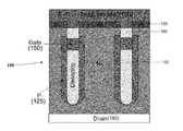
- FIG. 6shows some embodiments of methods for making a semiconductor structure with a source formed over the second oxide region and the contact region
- FIG. 7shows some embodiments of the operation of the semiconductor structure depicted in FIG. 6 ;
- FIGS. 8 and 9show some embodiments of the PN junctions that can be present in semiconductor structures.
- FIGS. 10( a ) and ( b )shows two conventional SIT semiconductor devices.
- planar or recessed gate SIT devicescould be modified for other static induction family devices, such as static induction thyristors, Static Induction Diode (SID), Static Induction Thyristor, Lateral Punch-Through Transistor (LPTT), Static Induction Transistor Logic (SITL), Static Induction MOS Transistor (SIMOS), Space Charge Limiting Load (SCLL), and the bipolar mode devices of all these devices (e.g. Bipolar Static Induction Transistor, Bipolar Static Induction Thyristor.
- SIDStatic Induction Diode
- LPTTLateral Punch-Through Transistor
- SITLStatic Induction Transistor Logic
- SIMOSStatic Induction MOS Transistor
- SCLLSpace Charge Limiting Load
- bipolar mode devices of all these devicese.g. Bipolar Static Induction Transistor, Bipolar Static Induction Thyristor.
- the devices of the inventionare described with reference to a particular type of conductivity (P or N), the devices can be configured with a combination of the same type of dopant or can be configured with the opposite type of conductivity (N or P, respectively) by appropriate modifications.
- FIGS. 1-7Some embodiments of the semiconductor devices and methods for making such device are shown in FIGS. 1-7 .
- the methodsbegin in some embodiments, as depicted in FIG. 1 , when a semiconductor substrate 105 is first provided. Any substrate known in the art can be used in the invention. Suitable substrates include silicon wafers, epitaxial Si layers, bonded wafers such as used in silicon-on-insulator (SOI) technologies, and/or amorphous silicon layers, all of which may be doped or undoped.
- SOIsilicon-on-insulator
- any other semiconducting material used for electronic devicescan be used, including Ge, SiGe, SiC, GaN, GaAs, In x Ga y As z , Al x Ga y As z , and/or any pure or compound semiconductors, such as III-V or II-VIs and their variants.
- the substrate 105can be heavily doped with any n-type dopant.
- the substrate 105contains one or more epitaxial (“epi”) Si layers (individually or collectively depicted as epitaxial layer 110 ) located on an upper surface thereof.
- the epitaxial layer(s) 110can be provided using any known process in the art, including any known epitaxial deposition process.
- the epitaxial layer(s)can be lightly doped with an n-type dopant.
- the dopant concentration within the epitaxial layer 110is not uniform.
- the epitaxial layer 110can have a higher dopant concentration in the upper portion and a lower dopant concentration in the lower portion.
- the epitaxial layercan have a concentration gradient throughout its depth with the highest concentration near or at the upper surface and the lower concentration near or at the interface with the substrate, or vice versa 105 .
- the concentration gradient along the lengthcan be a consistent decrease, a step-wise decrease, or a combination thereof.
- each epitaxial layercontains a different dopant concentration.
- the number of epitaxial layerscan range from 2 to as many as needed.
- each successive epitaxial layeris deposited on the underlying epitaxial layer (or substrate) while being in-situ doped to a higher concentration by any known method for epitaxial layer growth.
- epitaxial layers 110includes a first epitaxial Si layer with a first concentration, a second epitaxial Si layer with a higher concentration, a third epitaxial Si layer with an even higher concentration, and a fourth epitaxial Si layer with the highest concentration.
- a trench structure 120can be formed in the epitaxial layer 110 .
- the trench structure 120can be formed by any known process.
- a mask 115can be formed on the upper surface of the epitaxial layer 110 .
- the mask 115can be formed by first depositing a layer of the desired mask material and then patterning it using photolithography and etch process so the desired pattern for the mask 115 is formed.
- the epitaxial layer 110can then be etched by any known process until the trench 120 has reached the desired depth in the epitaxial layer 110 .
- the sidewall of the trenchis not perpendicular to the upper surface of the epitaxial layer 110 .
- the angle of the trench sidewallcan range from about 90 degrees (a vertical sidewall) to about 70 degrees relative to the upper surface of the epitaxial layer 110 .
- the sidewall of the trench structure 120can doped with a p-type dopant so that a sidewall dopant region 125 is formed on the trench sidewall.
- the sidewall doping processcan be performed using any doping process which implants the p-type dopants to the desired width in the sidewall of the trench structure. After the doping process, the dopants can be further diffused into the mesa region by any known diffusion or drive-in process. The width of the sidewall dopant region can be adjusted so that the mesa region adjacent to any trench can be partially or fully depleted when the device is off and blocking the current.
- the sidewall doping processcan be performed using any angled implant process, the gas phase doping process, a diffusion process, or a combination thereof. In other embodiments, an angled implantation process can be used with an angle ranging from about 0 degrees (a vertical implant process) to about 45 degrees.
- the width of the mesas 112 , the depth of the trenches 120 , the implantation angle, and the angle of the trench sidewallcan be used to determine the width and depth of the p-type doped region of the side wall. Accordingly, the depth of the trenches can range from about 0.1 to about 100 ⁇ m and the width of the mesas can range from about 0.1 to about 100 ⁇ m when the angle of the trench sidewall can range from about 90 degrees (a vertical sidewall) to about 70 degrees.
- the different dopant concentrations in the epitaxial layers 110help form a PN super-junction structure with a well defined PN junction.
- the sidewall angleWith the sidewall angle, the width of the trench decreases slightly as the depth of the trench increases.
- the p-type sidewall dopant region created in the n-type epitaxial layer 110will have a substantially similar angle. But the resulting structure at the PN junction contains an n-type region that is relatively larger than the p-type region, which can detract from the performance of the PN super-junction since it may not be charge balanced.
- FIG. 8illustrates a semiconductor structure containing p-regions 225 , an angled trench 205 , gate 210 , insulating layer 215 , and epitaxial layer 200 that contains a uniform dopant concentration.
- the p-regions 225 from one trench to anotherare separated by distance A in the N ⁇ region of the epitaxial layer. The distance A, however, is wider than is needed for proper charge balance and depletion.
- the epitaxial layer 200 ′contains the gradient dopant concentration described herein.
- This gradient concentrationallows the formation and adjustment of a p-region 225 ′ that has a wider bottom, making the distance A′ between the p-regions 225 ′ smaller than A. The result of this configuration allows a more change-balanced semiconductor structure relative to the structure in FIG. 8 .
- an oxide layer 130(or other insulating or semi-insulating material) can be formed in the trenches 120 .
- the oxide layer 130can be formed by any process known in the art.
- the oxide layer 130can be formed by depositing an oxide material until it overflows the trenches 120 .
- the deposition of the oxide materialcan be carried out using any known deposition process, including chemical vapor deposition (CVD) processes, such as SACVD.
- CVDchemical vapor deposition
- SACVDchemical vapor deposition
- the thickness of the oxide layer 130can be adjusted to any thickness needed to fill the trenches 120 . If needed, a reflow process can be used to reflow the oxide material, which will help reduce voids or defects within the oxide region.
- an etchback processcan be used to remove the excess oxide material that located is above the trenches 120 and on the mesas 112 .
- the upper surface of the oxide layer 120 and the mask 115are substantially coplanar, as depicted in FIG. 3 .
- a planarization processsuch as any chemical and/or mechanical polishing known in the art, can be used in addition to (whether before or after) or instead of the etchback process.
- a high quality oxide layercan be formed prior to depositing the oxide layer 130 .
- the high quality oxide layercan be formed by oxidizing the epitaxial layer 110 in an oxide-containing atmosphere until the desired thickness of the layer has been grown.
- the high quality oxide layercan be used to improve the oxide integrity and filling factor, thereby making the oxide layer 130 a better insulator.
- the mask 115is removed from the upper surface of the epitaxial layer 110 using any process known in the art.
- a contact region 135can be formed on the exposed upper surface of the epitaxial layer 110 (which is exposed when the mask 115 is removed).
- the contact region 135can be formed using any process known in the art.
- the contact regions 135can be formed by implanting an n-type dopant in the upper surface of the epitaxial layer 110 and then driving-in the dopant using any known process.
- an upper portion of the oxide layer 130 in the trenchcan be removed.
- the removal processcan be performed using any process known in the art, including an etchback process using a plasma etch process.
- the resulting structureis depicted in FIG. 4 where an upper part of the trench 120 does not contain an oxide material, but a first (or lower) oxide (or insulating) region 140 is formed in the bottom of the trenches 120 .
- a conductive layercan be deposited on the first oxide region 140 in the lower, middle, or upper part of the trench 120 .
- the conductive layercan comprise any conductive and/or semiconductive material known in the art including any metal, silicide, semiconducting material, doped polysilicon, or combinations thereof.
- the conductive layercan be deposited by any known deposition process, including chemical vapor deposition processes (CVD, PECVD, LPCVD) or sputtering processes using the desired metal as the sputtering target.
- the conductive layercan be deposited so that it fills the upper part of the trench 120 and overflows onto the upper part of the contact region 135 .
- a gate 150can be formed from the conductive layer using any process known in the art.
- the gate 150can be formed by removing the upper portion of the conductive layer using any process known the art, including any etchback process. The result of the removal process leaves a conductive layer (the gate 150 ) overlying the first oxide region 140 in the trench 120 , as shown in FIG. 4 .
- a second oxide layer(or second insulating or semi-insulating layer) can be deposited in the upper part of the trench 120 where the conductive layer has been removed (area 142 in FIG. 4 ).
- the second oxide layercan be formed by any process known in the art.
- the second oxide layeris formed by depositing an oxide material until it overflows the upper part 142 of the trenches 120 .
- the deposition of the oxide materialcan be carried out using any known deposition process, including chemical vapor deposition (CVD) processes such as SACVD.
- the thickness of the second oxide layercan be adjusted to the thickness needed fill the upper part 142 of the trench 120 . If needed, a reflow process can be used to reflow the oxide material in the second oxide layer.
- an etchback processcan be used to remove the amount of the material that is above the contact region 135 and above the trench 120 .
- a source layer (or region) 170can be deposited over the upper portions of the second oxide region 160 and the contact region 135 .
- the source layer 170can comprise any conductive and/or semiconductive material known in the art, including any metal, silicide, polysilicon, or combinations thereof.
- the source layer 170can be deposited by any known deposition process, including chemical vapor deposition processes (CVD, PECVD, LPCVD) or sputtering processes using the desired metal as the sputtering target.
- a drain 180can be formed on the backside of the substrate 105 using any process known in the art.
- the drain 180can be formed on the backside by thinning the backside of the substrate 105 using any process known in the art, including a grinding, polishing, or etch processes.
- a conductive layercan be deposited on the backside of the substrate 105 as known in the art until the desired thickness of the conductive layer of the drain is formed.
- the semiconductor device 100contains a source layer 170 that is located in an upper portion of the device 100 and a drain 180 located in the bottom portion of the device.
- the gate 150is vertically isolated between the first oxide region 140 and the second oxide region 160 .
- the gate 150is connected to the p-type sidewall dopant regions 125 which, along with the n-type epitaxial layer 110 , form the PN junction of a super-junction structure. With such a configuration, the gate can be used to control the current path in the semiconductor device 100 .
- the operation of the semiconductor device 100is similar to these two SIT devices.
- the semiconductor deviceoperates normally in an off-state with the gate voltage equal to 0. But when a reverse bias is applied to the gate, the depletion region 180 can expand and pinch off the drift region, as shown in FIG. 7 .
- the semiconductor device 100also improves on the device characteristics of both planar SIT and recessed gate SIT devices.
- planar gate SIT devices(as shown in FIG. 8 a ) can have relatively low capacitance but a high R sp while recessed gate SIT devices can have low R sp but a high capacitance.
- the first improvement of the device 100 over these SIT devicesis that the R sp of the semiconductor device 100 depicted in FIG. 6 can be significantly lower than the planar gate SIT devices. This improvement results from the higher doping concentration in the channel and drift regions that can be achieved by first, charge balancing with the trench super-junction and second, by the methods for defining the smaller features and controlling the diffusion in the sidewall implant process.
- the second improvementis that the capacitance of the semiconductor device 100 can be significantly lower than the recessed gate SIT devices because the parasitic capacitance from the gate connection from the surface can be virtually removed.
- a third improvement over these SIT devicesrelates to the die size. Given that different die sizes are often needed to achieve an equivalent Rds on for a semiconductor device, the actual capacitance of the semiconductor device 100 for a given die size is much smaller than both of these SIT devices.
- a fourth improvement over these SIT devicesrelates to the parasitic capacitance. Since the gate of the semiconductor device 100 is isolated by using the first oxide region 140 and second oxide region 160 in the trench 120 , the parasitic capacitance can be reduced relative to recessed gate SIT devices since the recessed gate SIT has large parasitic capacitance from the sidewall insulation and the gate connection material.
- a fifth improvementrelates to the drift region of the device.
- the drift region doping concentrationshould be as low as possible to achieve high breakdown voltage. But this often results in relatively high on-resistance.
- combining the SIT (or JFET) structures in a trench with a super-junction structurecan increase the drift doping concentration and can also define a smaller pitch that is able to improve both the current conductivity and the frequency (the switching speed).
- the drift region doping concentrationcan be much higher than the conventional SIT or JFET structure.
- one or more of the various dielectric layers in the embodiments described hereinmay comprise low-k or high-k dielectric materials.
- specific dopantsare names for the n-type and p-type dopants, any other known n-type and p-type dopants (or combination of such dopants) can be used in the semiconductor devices.
- the devices of the inventionare described with reference to a particular type of conductivity (P or N), the devices can be configured with a combination of the same type of dopant or can be configured with the opposite type of conductivity (N or P, respectively) by appropriate modifications.
- a method for making a semiconductor devicecomprises providing a semiconductor substrate heavily doped with a dopant of a first conductivity type, providing an epitaxial layer on the substrate, the epitaxial layer being lightly doped with a dopant of a first conductivity type with a concentration gradient, providing a trench formed in the epitaxial layer, the trench containing a sidewall that is lightly doped with a dopant of a second conductivity type, a first insulating region in a lower portion of the trench and a second insulating region in an upper portion of the trench, the first and second insulating regions sandwiching a conductive layer, providing a source layer contacting the upper surface of the epitaxial layer and the upper surface of the second insulating region, and providing a drain contacting a bottom portion of the substrate.
- a method for making a semiconductor devicecomprises providing a semiconductor substrate heavily doped with a dopant of a first conductivity type, providing an epitaxial layer on the substrate, the epitaxial layer being lightly doped with a dopant of a first conductivity type with a concentration gradient, providing a contact region on the upper surface of the epitaxial layer, the contact region being heavily doped with a dopant of a first conductivity type, providing a trench formed in the epitaxial layer, the trench containing a sidewall that is lightly doped with a dopant of a second conductivity type to form a super-junction with the epitaxial layer, and the trench containing a gate electrically connected to the sidewall and insulated by upper and lower insulating regions in the trench, providing a source layer contacting the upper surface of the epitaxial layer and the upper surface of the upper insulating region, and providing a drain contacting a bottom portion of the substrate.
- a method for making a semiconductor devicecomprises providing a semiconductor substrate heavily doped with a dopant of a first conductivity type, depositing an epitaxial layer on the substrate, the epitaxial layer being lightly doped with a dopant of a first conductivity type and containing a decreasing dopant concentration as it approaches the substrate, forming a trench in the epitaxial layer, the trench containing a sidewall angle ranging from about 90 (vertical side wall) to about 70 degrees, forming a dopant region in the trench sidewall using an angled implantation process, the dopant region being lightly doped with a dopant of a second conductivity type, forming a first insulating region in a lower portion of the trench, forming a contact region on the upper surface of the epitaxial layer, the contact region being heavily doped with a dopant of a first conductivity type, forming a conductive gate on the first insulating region, forming a second insulating region on the conductive gate, depositing
Landscapes
- Junction Field-Effect Transistors (AREA)
Abstract
Description
Claims (20)
Priority Applications (1)
| Application Number | Priority Date | Filing Date | Title |
|---|---|---|---|
| US12/629,232US8129778B2 (en) | 2009-12-02 | 2009-12-02 | Semiconductor devices and methods for making the same |
Applications Claiming Priority (1)
| Application Number | Priority Date | Filing Date | Title |
|---|---|---|---|
| US12/629,232US8129778B2 (en) | 2009-12-02 | 2009-12-02 | Semiconductor devices and methods for making the same |
Publications (2)
| Publication Number | Publication Date |
|---|---|
| US20110127601A1 US20110127601A1 (en) | 2011-06-02 |
| US8129778B2true US8129778B2 (en) | 2012-03-06 |
Family
ID=44068204
Family Applications (1)
| Application Number | Title | Priority Date | Filing Date |
|---|---|---|---|
| US12/629,232Active2030-09-17US8129778B2 (en) | 2009-12-02 | 2009-12-02 | Semiconductor devices and methods for making the same |
Country Status (1)
| Country | Link |
|---|---|
| US (1) | US8129778B2 (en) |
Cited By (1)
| Publication number | Priority date | Publication date | Assignee | Title |
|---|---|---|---|---|
| US8906807B2 (en) | 2012-10-10 | 2014-12-09 | International Business Machines Corporation | Single fin cut employing angled processing methods |
Families Citing this family (4)
| Publication number | Priority date | Publication date | Assignee | Title |
|---|---|---|---|---|
| US20110198689A1 (en)* | 2010-02-17 | 2011-08-18 | Suku Kim | Semiconductor devices containing trench mosfets with superjunctions |
| CN109346523A (en)* | 2018-09-28 | 2019-02-15 | 张帅 | Trench gate field effect transistor with super junction structure and method of making the same |
| CN113937156B (en)* | 2021-10-11 | 2023-07-04 | 上海华虹宏力半导体制造有限公司 | Semiconductor structure and forming method thereof |
| CN116544268B (en)* | 2023-07-06 | 2023-09-26 | 通威微电子有限公司 | Semiconductor device structure and manufacturing method thereof |
Citations (36)
| Publication number | Priority date | Publication date | Assignee | Title |
|---|---|---|---|---|
| US4348690A (en)* | 1981-04-30 | 1982-09-07 | Rca Corporation | Semiconductor imagers |
| US4666557A (en)* | 1984-12-10 | 1987-05-19 | Ncr Corporation | Method for forming channel stops in vertical semiconductor surfaces |
| US4713358A (en) | 1986-05-02 | 1987-12-15 | Gte Laboratories Incorporated | Method of fabricating recessed gate static induction transistors |
| US5034338A (en)* | 1986-08-13 | 1991-07-23 | Siemens Aktiengesellschaft | Circuit containing integrated bipolar and complementary MOS transistors on a common substrate |
| US5250461A (en)* | 1991-05-17 | 1993-10-05 | Delco Electronics Corporation | Method for dielectrically isolating integrated circuits using doped oxide sidewalls |
| US5250837A (en)* | 1991-05-17 | 1993-10-05 | Delco Electronics Corporation | Method for dielectrically isolating integrated circuits using doped oxide sidewalls |
| US5352915A (en)* | 1992-08-11 | 1994-10-04 | U.S. Philips Corporation | Semiconductor component having two integrated insulated gate field effect devices |
| US5583348A (en)* | 1991-12-03 | 1996-12-10 | Motorola, Inc. | Method for making a schottky diode that is compatible with high performance transistor structures |
| US5689128A (en)* | 1995-08-21 | 1997-11-18 | Siliconix Incorporated | High density trenched DMOS transistor |
| US5753938A (en)* | 1996-08-08 | 1998-05-19 | North Carolina State University | Static-induction transistors having heterojunction gates and methods of forming same |
| US5770484A (en)* | 1996-12-13 | 1998-06-23 | International Business Machines Corporation | Method of making silicon on insulator buried plate trench capacitor |
| US6057184A (en)* | 1997-03-21 | 2000-05-02 | International Business Machines Corporation | Semiconductor device fabrication method using connecting implants |
| US6090661A (en)* | 1998-03-19 | 2000-07-18 | Lsi Logic Corporation | Formation of novel DRAM cell capacitors by integration of capacitors with isolation trench sidewalls |
| US6228698B1 (en)* | 1998-04-17 | 2001-05-08 | U.S. Philips Corporation | Manufacture of field-effect semiconductor devices |
| US6285060B1 (en)* | 1999-12-30 | 2001-09-04 | Siliconix Incorporated | Barrier accumulation-mode MOSFET |
| US6291298B1 (en)* | 1999-05-25 | 2001-09-18 | Advanced Analogic Technologies, Inc. | Process of manufacturing Trench gate semiconductor device having gate oxide layer with multiple thicknesses |
| US6677641B2 (en) | 2001-10-17 | 2004-01-13 | Fairchild Semiconductor Corporation | Semiconductor structure with improved smaller forward voltage loss and higher blocking capability |
| US6710418B1 (en)* | 2002-10-11 | 2004-03-23 | Fairchild Semiconductor Corporation | Schottky rectifier with insulation-filled trenches and method of forming the same |
| US6803626B2 (en) | 2002-07-18 | 2004-10-12 | Fairchild Semiconductor Corporation | Vertical charge control semiconductor device |
| US6818513B2 (en) | 2001-01-30 | 2004-11-16 | Fairchild Semiconductor Corporation | Method of forming a field effect transistor having a lateral depletion structure |
| US6878993B2 (en)* | 2002-12-20 | 2005-04-12 | Hamza Yilmaz | Self-aligned trench MOS junction field-effect transistor for high-frequency applications |
| US20050167744A1 (en)* | 2004-02-02 | 2005-08-04 | Hamza Yilmaz | Semiconductor device containing dielectrically isolated PN junction for enhanced breakdown characteristics |
| US6987052B2 (en)* | 2003-10-30 | 2006-01-17 | Agere Systems Inc. | Method for making enhanced substrate contact for a semiconductor device |
| US7026668B2 (en) | 2002-03-25 | 2006-04-11 | Kabushiki Kaisha Toshiba | High-breakdown-voltage semiconductor device |
| US7052982B2 (en) | 2003-12-19 | 2006-05-30 | Third Dimension (3D) Semiconductor, Inc. | Method for manufacturing a superjunction device with wide mesas |
| US20070131987A1 (en)* | 2005-12-09 | 2007-06-14 | Dongbu Electronics Co., Ltd. | Vertical image sensor and method for manufacturing the same |
| US7319256B1 (en) | 2006-06-19 | 2008-01-15 | Fairchild Semiconductor Corporation | Shielded gate trench FET with the shield and gate electrodes being connected together |
| US7332398B2 (en)* | 2002-12-14 | 2008-02-19 | Nxp B.V. | Manufacture of trench-gate semiconductor devices |
| US7345342B2 (en) | 2001-01-30 | 2008-03-18 | Fairchild Semiconductor Corporation | Power semiconductor devices and methods of manufacture |
| US7368777B2 (en) | 2003-12-30 | 2008-05-06 | Fairchild Semiconductor Corporation | Accumulation device with charge balance structure and method of forming the same |
| US20080111207A1 (en) | 2006-11-15 | 2008-05-15 | Lee Jae-Gil | High-Voltage Semiconductor Device and Method of Fabricating the Same |
| US20080138954A1 (en) | 2006-06-16 | 2008-06-12 | Fairchild Semiconductor Corporation | High voltage ldmos |
| US7394144B2 (en)* | 2004-03-31 | 2008-07-01 | Nxp B.V. | Trench semiconductor device and method of manufacturing it |
| US7393749B2 (en) | 2005-06-10 | 2008-07-01 | Fairchild Semiconductor Corporation | Charge balance field effect transistor |
| US7910486B2 (en)* | 2009-06-12 | 2011-03-22 | Alpha & Omega Semiconductor, Inc. | Method for forming nanotube semiconductor devices |
| US20110198689A1 (en)* | 2010-02-17 | 2011-08-18 | Suku Kim | Semiconductor devices containing trench mosfets with superjunctions |
- 2009
- 2009-12-02USUS12/629,232patent/US8129778B2/enactiveActive
Patent Citations (38)
| Publication number | Priority date | Publication date | Assignee | Title |
|---|---|---|---|---|
| US4348690A (en)* | 1981-04-30 | 1982-09-07 | Rca Corporation | Semiconductor imagers |
| US4666557A (en)* | 1984-12-10 | 1987-05-19 | Ncr Corporation | Method for forming channel stops in vertical semiconductor surfaces |
| US4713358A (en) | 1986-05-02 | 1987-12-15 | Gte Laboratories Incorporated | Method of fabricating recessed gate static induction transistors |
| US5034338A (en)* | 1986-08-13 | 1991-07-23 | Siemens Aktiengesellschaft | Circuit containing integrated bipolar and complementary MOS transistors on a common substrate |
| US5250461A (en)* | 1991-05-17 | 1993-10-05 | Delco Electronics Corporation | Method for dielectrically isolating integrated circuits using doped oxide sidewalls |
| US5250837A (en)* | 1991-05-17 | 1993-10-05 | Delco Electronics Corporation | Method for dielectrically isolating integrated circuits using doped oxide sidewalls |
| US5583348A (en)* | 1991-12-03 | 1996-12-10 | Motorola, Inc. | Method for making a schottky diode that is compatible with high performance transistor structures |
| US5352915A (en)* | 1992-08-11 | 1994-10-04 | U.S. Philips Corporation | Semiconductor component having two integrated insulated gate field effect devices |
| US5689128A (en)* | 1995-08-21 | 1997-11-18 | Siliconix Incorporated | High density trenched DMOS transistor |
| US5753938A (en)* | 1996-08-08 | 1998-05-19 | North Carolina State University | Static-induction transistors having heterojunction gates and methods of forming same |
| US5770484A (en)* | 1996-12-13 | 1998-06-23 | International Business Machines Corporation | Method of making silicon on insulator buried plate trench capacitor |
| US6057184A (en)* | 1997-03-21 | 2000-05-02 | International Business Machines Corporation | Semiconductor device fabrication method using connecting implants |
| US6090661A (en)* | 1998-03-19 | 2000-07-18 | Lsi Logic Corporation | Formation of novel DRAM cell capacitors by integration of capacitors with isolation trench sidewalls |
| US6228698B1 (en)* | 1998-04-17 | 2001-05-08 | U.S. Philips Corporation | Manufacture of field-effect semiconductor devices |
| US6291298B1 (en)* | 1999-05-25 | 2001-09-18 | Advanced Analogic Technologies, Inc. | Process of manufacturing Trench gate semiconductor device having gate oxide layer with multiple thicknesses |
| US6285060B1 (en)* | 1999-12-30 | 2001-09-04 | Siliconix Incorporated | Barrier accumulation-mode MOSFET |
| US7345342B2 (en) | 2001-01-30 | 2008-03-18 | Fairchild Semiconductor Corporation | Power semiconductor devices and methods of manufacture |
| US6818513B2 (en) | 2001-01-30 | 2004-11-16 | Fairchild Semiconductor Corporation | Method of forming a field effect transistor having a lateral depletion structure |
| US6677641B2 (en) | 2001-10-17 | 2004-01-13 | Fairchild Semiconductor Corporation | Semiconductor structure with improved smaller forward voltage loss and higher blocking capability |
| US7026668B2 (en) | 2002-03-25 | 2006-04-11 | Kabushiki Kaisha Toshiba | High-breakdown-voltage semiconductor device |
| US6803626B2 (en) | 2002-07-18 | 2004-10-12 | Fairchild Semiconductor Corporation | Vertical charge control semiconductor device |
| US6710418B1 (en)* | 2002-10-11 | 2004-03-23 | Fairchild Semiconductor Corporation | Schottky rectifier with insulation-filled trenches and method of forming the same |
| US7332398B2 (en)* | 2002-12-14 | 2008-02-19 | Nxp B.V. | Manufacture of trench-gate semiconductor devices |
| US6878993B2 (en)* | 2002-12-20 | 2005-04-12 | Hamza Yilmaz | Self-aligned trench MOS junction field-effect transistor for high-frequency applications |
| US6987052B2 (en)* | 2003-10-30 | 2006-01-17 | Agere Systems Inc. | Method for making enhanced substrate contact for a semiconductor device |
| US7052982B2 (en) | 2003-12-19 | 2006-05-30 | Third Dimension (3D) Semiconductor, Inc. | Method for manufacturing a superjunction device with wide mesas |
| US7368777B2 (en) | 2003-12-30 | 2008-05-06 | Fairchild Semiconductor Corporation | Accumulation device with charge balance structure and method of forming the same |
| US20050167744A1 (en)* | 2004-02-02 | 2005-08-04 | Hamza Yilmaz | Semiconductor device containing dielectrically isolated PN junction for enhanced breakdown characteristics |
| US7323386B2 (en)* | 2004-02-02 | 2008-01-29 | Hamza Yilmaz | Method of fabricating semiconductor device containing dielectrically isolated PN junction for enhanced breakdown characteristics |
| US7394144B2 (en)* | 2004-03-31 | 2008-07-01 | Nxp B.V. | Trench semiconductor device and method of manufacturing it |
| US7393749B2 (en) | 2005-06-10 | 2008-07-01 | Fairchild Semiconductor Corporation | Charge balance field effect transistor |
| US20090191678A1 (en)* | 2005-06-10 | 2009-07-30 | Hamza Yilmaz | Method of Forming a Shielded Gate Field Effect Transistor |
| US20070131987A1 (en)* | 2005-12-09 | 2007-06-14 | Dongbu Electronics Co., Ltd. | Vertical image sensor and method for manufacturing the same |
| US20080138954A1 (en) | 2006-06-16 | 2008-06-12 | Fairchild Semiconductor Corporation | High voltage ldmos |
| US7319256B1 (en) | 2006-06-19 | 2008-01-15 | Fairchild Semiconductor Corporation | Shielded gate trench FET with the shield and gate electrodes being connected together |
| US20080111207A1 (en) | 2006-11-15 | 2008-05-15 | Lee Jae-Gil | High-Voltage Semiconductor Device and Method of Fabricating the Same |
| US7910486B2 (en)* | 2009-06-12 | 2011-03-22 | Alpha & Omega Semiconductor, Inc. | Method for forming nanotube semiconductor devices |
| US20110198689A1 (en)* | 2010-02-17 | 2011-08-18 | Suku Kim | Semiconductor devices containing trench mosfets with superjunctions |
Cited By (1)
| Publication number | Priority date | Publication date | Assignee | Title |
|---|---|---|---|---|
| US8906807B2 (en) | 2012-10-10 | 2014-12-09 | International Business Machines Corporation | Single fin cut employing angled processing methods |
Also Published As
| Publication number | Publication date |
|---|---|
| US20110127601A1 (en) | 2011-06-02 |
Similar Documents
| Publication | Publication Date | Title |
|---|---|---|
| US20120018800A1 (en) | Trench Superjunction MOSFET with Thin EPI Process | |
| US20200395451A1 (en) | Thin poly field plate design | |
| KR101294917B1 (en) | Semiconductor devices containing trench mosfet with superjunctions | |
| US7033891B2 (en) | Trench gate laterally diffused MOSFET devices and methods for making such devices | |
| US9466700B2 (en) | Semiconductor device and method of fabricating same | |
| US9306058B2 (en) | Integrated circuit and method of manufacturing an integrated circuit | |
| US9209277B2 (en) | Manufacturing methods for laterally diffused metal oxide semiconductor devices | |
| US9159791B2 (en) | Semiconductor device comprising a conductive region | |
| US20130087852A1 (en) | Edge termination structure for power semiconductor devices | |
| US20140273374A1 (en) | Vertical Doping and Capacitive Balancing for Power Semiconductor Devices | |
| US7601568B2 (en) | MOS transistor and method for producing a MOS transistor structure | |
| KR20120106578A (en) | Mosfet device with thick trench bottom oxide | |
| US8129778B2 (en) | Semiconductor devices and methods for making the same | |
| US20130224922A1 (en) | UMOS Semiconductor Devices Formed by Low Temperature Processing | |
| US11705506B2 (en) | Lateral trench transistor device | |
| US8816429B2 (en) | Charge balance semiconductor devices with increased mobility structures | |
| US20240413239A1 (en) | Ldmos nanosheet transistor | |
| US7510957B2 (en) | Complimentary lateral III-nitride transistors |
Legal Events
| Date | Code | Title | Description |
|---|---|---|---|
| AS | Assignment | Owner name:FAIRCHILD SEMICONDUCTOR CORPORATION, CALIFORNIA Free format text:ASSIGNMENT OF ASSIGNORS INTEREST;ASSIGNORS:KIM, SUKU;MURPHY, JAMES J.;DOLNY, GARY;SIGNING DATES FROM 20110603 TO 20110606;REEL/FRAME:026392/0853 | |
| STCF | Information on status: patent grant | Free format text:PATENTED CASE | |
| FPAY | Fee payment | Year of fee payment:4 | |
| AS | Assignment | Owner name:DEUTSCHE BANK AG NEW YORK BRANCH, AS COLLATERAL AGENT, NEW YORK Free format text:PATENT SECURITY AGREEMENT;ASSIGNOR:FAIRCHILD SEMICONDUCTOR CORPORATION;REEL/FRAME:040075/0644 Effective date:20160916 Owner name:DEUTSCHE BANK AG NEW YORK BRANCH, AS COLLATERAL AG Free format text:PATENT SECURITY AGREEMENT;ASSIGNOR:FAIRCHILD SEMICONDUCTOR CORPORATION;REEL/FRAME:040075/0644 Effective date:20160916 | |
| MAFP | Maintenance fee payment | Free format text:PAYMENT OF MAINTENANCE FEE, 8TH YEAR, LARGE ENTITY (ORIGINAL EVENT CODE: M1552); ENTITY STATUS OF PATENT OWNER: LARGE ENTITY Year of fee payment:8 | |
| AS | Assignment | Owner name:SEMICONDUCTOR COMPONENTS INDUSTRIES, LLC, ARIZONA Free format text:ASSIGNMENT OF ASSIGNORS INTEREST;ASSIGNOR:FAIRCHILD SEMICONDUCTOR CORPORATION;REEL/FRAME:057694/0374 Effective date:20210722 | |
| AS | Assignment | Owner name:FAIRCHILD SEMICONDUCTOR CORPORATION, ARIZONA Free format text:RELEASE BY SECURED PARTY;ASSIGNOR:DEUTSCHE BANK AG NEW YORK BRANCH;REEL/FRAME:057969/0206 Effective date:20211027 | |
| AS | Assignment | Owner name:DEUTSCHE BANK AG NEW YORK BRANCH, AS COLLATERAL AGENT, NEW YORK Free format text:SECURITY INTEREST;ASSIGNOR:SEMICONDUCTOR COMPONENTS INDUSTRIES, LLC;REEL/FRAME:058871/0799 Effective date:20211028 | |
| AS | Assignment | Owner name:FAIRCHILD SEMICONDUCTOR CORPORATION, ARIZONA Free format text:RELEASE OF SECURITY INTEREST IN PATENTS RECORDED AT REEL 040075, FRAME 0644;ASSIGNOR:DEUTSCHE BANK AG NEW YORK BRANCH, AS COLLATERAL AGENT;REEL/FRAME:064070/0536 Effective date:20230622 Owner name:SEMICONDUCTOR COMPONENTS INDUSTRIES, LLC, ARIZONA Free format text:RELEASE OF SECURITY INTEREST IN PATENTS RECORDED AT REEL 040075, FRAME 0644;ASSIGNOR:DEUTSCHE BANK AG NEW YORK BRANCH, AS COLLATERAL AGENT;REEL/FRAME:064070/0536 Effective date:20230622 | |
| AS | Assignment | Owner name:FAIRCHILD SEMICONDUCTOR CORPORATION, ARIZONA Free format text:RELEASE OF SECURITY INTEREST IN PATENTS RECORDED AT REEL 058871, FRAME 0799;ASSIGNOR:DEUTSCHE BANK AG NEW YORK BRANCH, AS COLLATERAL AGENT;REEL/FRAME:065653/0001 Effective date:20230622 Owner name:SEMICONDUCTOR COMPONENTS INDUSTRIES, LLC, ARIZONA Free format text:RELEASE OF SECURITY INTEREST IN PATENTS RECORDED AT REEL 058871, FRAME 0799;ASSIGNOR:DEUTSCHE BANK AG NEW YORK BRANCH, AS COLLATERAL AGENT;REEL/FRAME:065653/0001 Effective date:20230622 | |
| MAFP | Maintenance fee payment | Free format text:PAYMENT OF MAINTENANCE FEE, 12TH YEAR, LARGE ENTITY (ORIGINAL EVENT CODE: M1553); ENTITY STATUS OF PATENT OWNER: LARGE ENTITY Year of fee payment:12 |