US8128993B2 - Anisotropic nanotube fabric layers and films and methods of forming same - Google Patents
Anisotropic nanotube fabric layers and films and methods of forming sameDownload PDFInfo
- Publication number
- US8128993B2 US8128993B2US12/533,695US53369509AUS8128993B2US 8128993 B2US8128993 B2US 8128993B2US 53369509 AUS53369509 AUS 53369509AUS 8128993 B2US8128993 B2US 8128993B2
- Authority
- US
- United States
- Prior art keywords
- nanotube
- layer
- adhesion
- elements
- averter
- Prior art date
- Legal status (The legal status is an assumption and is not a legal conclusion. Google has not performed a legal analysis and makes no representation as to the accuracy of the status listed.)
- Active, expires
Links
Images


Classifications
- H—ELECTRICITY
- H05—ELECTRIC TECHNIQUES NOT OTHERWISE PROVIDED FOR
- H05K—PRINTED CIRCUITS; CASINGS OR CONSTRUCTIONAL DETAILS OF ELECTRIC APPARATUS; MANUFACTURE OF ASSEMBLAGES OF ELECTRICAL COMPONENTS
- H05K3/00—Apparatus or processes for manufacturing printed circuits
- H05K3/02—Apparatus or processes for manufacturing printed circuits in which the conductive material is applied to the surface of the insulating support and is thereafter removed from such areas of the surface which are not intended for current conducting or shielding
- H05K3/04—Apparatus or processes for manufacturing printed circuits in which the conductive material is applied to the surface of the insulating support and is thereafter removed from such areas of the surface which are not intended for current conducting or shielding the conductive material being removed mechanically, e.g. by punching
- H05K3/046—Apparatus or processes for manufacturing printed circuits in which the conductive material is applied to the surface of the insulating support and is thereafter removed from such areas of the surface which are not intended for current conducting or shielding the conductive material being removed mechanically, e.g. by punching by selective transfer or selective detachment of a conductive layer
- H05K3/048—Apparatus or processes for manufacturing printed circuits in which the conductive material is applied to the surface of the insulating support and is thereafter removed from such areas of the surface which are not intended for current conducting or shielding the conductive material being removed mechanically, e.g. by punching by selective transfer or selective detachment of a conductive layer using a lift-off resist pattern or a release layer pattern
- B—PERFORMING OPERATIONS; TRANSPORTING
- B82—NANOTECHNOLOGY
- B82Y—SPECIFIC USES OR APPLICATIONS OF NANOSTRUCTURES; MEASUREMENT OR ANALYSIS OF NANOSTRUCTURES; MANUFACTURE OR TREATMENT OF NANOSTRUCTURES
- B82Y30/00—Nanotechnology for materials or surface science, e.g. nanocomposites
- B—PERFORMING OPERATIONS; TRANSPORTING
- B82—NANOTECHNOLOGY
- B82Y—SPECIFIC USES OR APPLICATIONS OF NANOSTRUCTURES; MEASUREMENT OR ANALYSIS OF NANOSTRUCTURES; MANUFACTURE OR TREATMENT OF NANOSTRUCTURES
- B82Y40/00—Manufacture or treatment of nanostructures
- C—CHEMISTRY; METALLURGY
- C01—INORGANIC CHEMISTRY
- C01B—NON-METALLIC ELEMENTS; COMPOUNDS THEREOF; METALLOIDS OR COMPOUNDS THEREOF NOT COVERED BY SUBCLASS C01C
- C01B32/00—Carbon; Compounds thereof
- C01B32/15—Nano-sized carbon materials
- C01B32/158—Carbon nanotubes
- H—ELECTRICITY
- H05—ELECTRIC TECHNIQUES NOT OTHERWISE PROVIDED FOR
- H05K—PRINTED CIRCUITS; CASINGS OR CONSTRUCTIONAL DETAILS OF ELECTRIC APPARATUS; MANUFACTURE OF ASSEMBLAGES OF ELECTRICAL COMPONENTS
- H05K3/00—Apparatus or processes for manufacturing printed circuits
- H05K3/10—Apparatus or processes for manufacturing printed circuits in which conductive material is applied to the insulating support in such a manner as to form the desired conductive pattern
- H05K3/12—Apparatus or processes for manufacturing printed circuits in which conductive material is applied to the insulating support in such a manner as to form the desired conductive pattern using thick film techniques, e.g. printing techniques to apply the conductive material or similar techniques for applying conductive paste or ink patterns
- H05K3/1208—Pretreatment of the circuit board, e.g. modifying wetting properties; Patterning by using affinity patterns
- H—ELECTRICITY
- H10—SEMICONDUCTOR DEVICES; ELECTRIC SOLID-STATE DEVICES NOT OTHERWISE PROVIDED FOR
- H10K—ORGANIC ELECTRIC SOLID-STATE DEVICES
- H10K71/00—Manufacture or treatment specially adapted for the organic devices covered by this subclass
- H10K71/60—Forming conductive regions or layers, e.g. electrodes
- H10K71/611—Forming conductive regions or layers, e.g. electrodes using printing deposition, e.g. ink jet printing
- B—PERFORMING OPERATIONS; TRANSPORTING
- B05—SPRAYING OR ATOMISING IN GENERAL; APPLYING FLUENT MATERIALS TO SURFACES, IN GENERAL
- B05D—PROCESSES FOR APPLYING FLUENT MATERIALS TO SURFACES, IN GENERAL
- B05D1/00—Processes for applying liquids or other fluent materials
- B05D1/18—Processes for applying liquids or other fluent materials performed by dipping
- B05D1/20—Processes for applying liquids or other fluent materials performed by dipping substances to be applied floating on a fluid
- B05D1/202—Langmuir Blodgett films (LB films)
- H—ELECTRICITY
- H05—ELECTRIC TECHNIQUES NOT OTHERWISE PROVIDED FOR
- H05K—PRINTED CIRCUITS; CASINGS OR CONSTRUCTIONAL DETAILS OF ELECTRIC APPARATUS; MANUFACTURE OF ASSEMBLAGES OF ELECTRICAL COMPONENTS
- H05K2201/00—Indexing scheme relating to printed circuits covered by H05K1/00
- H05K2201/02—Fillers; Particles; Fibers; Reinforcement materials
- H05K2201/0203—Fillers and particles
- H05K2201/0242—Shape of an individual particle
- H05K2201/026—Nanotubes or nanowires
- H—ELECTRICITY
- H05—ELECTRIC TECHNIQUES NOT OTHERWISE PROVIDED FOR
- H05K—PRINTED CIRCUITS; CASINGS OR CONSTRUCTIONAL DETAILS OF ELECTRIC APPARATUS; MANUFACTURE OF ASSEMBLAGES OF ELECTRICAL COMPONENTS
- H05K2201/00—Indexing scheme relating to printed circuits covered by H05K1/00
- H05K2201/03—Conductive materials
- H05K2201/032—Materials
- H05K2201/0323—Carbon
- H—ELECTRICITY
- H05—ELECTRIC TECHNIQUES NOT OTHERWISE PROVIDED FOR
- H05K—PRINTED CIRCUITS; CASINGS OR CONSTRUCTIONAL DETAILS OF ELECTRIC APPARATUS; MANUFACTURE OF ASSEMBLAGES OF ELECTRICAL COMPONENTS
- H05K2203/00—Indexing scheme relating to apparatus or processes for manufacturing printed circuits covered by H05K3/00
- H05K2203/11—Treatments characterised by their effect, e.g. heating, cooling, roughening
- H05K2203/1173—Differences in wettability, e.g. hydrophilic or hydrophobic areas
- H—ELECTRICITY
- H10—SEMICONDUCTOR DEVICES; ELECTRIC SOLID-STATE DEVICES NOT OTHERWISE PROVIDED FOR
- H10K—ORGANIC ELECTRIC SOLID-STATE DEVICES
- H10K30/00—Organic devices sensitive to infrared radiation, light, electromagnetic radiation of shorter wavelength or corpuscular radiation
- H10K30/80—Constructional details
- H10K30/81—Electrodes
- H10K30/82—Transparent electrodes, e.g. indium tin oxide [ITO] electrodes
- H10K30/821—Transparent electrodes, e.g. indium tin oxide [ITO] electrodes comprising carbon nanotubes
Definitions
- the present inventionrelates generally to nanotube fabric layers and films and, more specifically, to anisotropic nanotube fabrics layers and films and methods of forming same.
- Nonvolatile Nanotube Diodes and Nonvolatile Nanotube Blocks and Systems Using Same and Methods of Making Same(U.S. patent application Ser. No. 11/835,856), filed Aug. 8, 2008;
- Microstrip Antenna Elements and ArraysComprising a Shaped Nanotube Layer and Integrated Two Terminal Nanotube Select Devices (U.S. patent application Ser. No. 12/533,687) filed on even date herewith.
- Nanotube fabric layers and filmsare used in a plurality of electronic structures, and devices.
- U.S. patent application Ser. No. 11/835,856 to Bertin et al.incorporated herein by reference in its entirety, teaches methods of using nanotube fabric layers to realize nonvolatile devices such as, but not limited to, block switches, programmable resistive elements, and programmable logic devices.
- U.S. Pat. No. 7,365,632 to Bertin et al., incorporated herein by reference in its entiretyteaches the use of such fabric layers and films within the fabrication of thin film nanotube based resistors.
- nanotube elementscan be rendered conducting, non-conducting, or semi-conducting before or after the formation of a nanotube fabric layer or film, allowing such nanotube fabric layers and films to serve a plurality of functions within an electronic device or system.
- the electrical conductivity of a nanotube fabric layer or filmcan be adjusted between two or more non-volatile states as taught in U.S. patent application Ser. No. 11/280,786, now U.S. Pat. No. 7,781,862, to Bertin et al., incorporated herein by reference in its entirety, allowing for such nanotube fabric layers and films to be used as memory or logic elements within an electronic system.
- U.S. Pat. No. 7,334,395 to Ward et al.incorporated herein by reference in its entirety, teaches a plurality of methods for forming nanotube fabric layers and films on a substrate element using preformed nanotubes.
- the methodsinclude, but are not limited to, spin coating (wherein a solution of nanotubes is deposited on a substrate which is then spun to evenly distribute said solution across the surface of said substrate), spray coating (wherein a plurality of nanotube are suspended within an aerosol solution which is then disbursed over a substrate), and in situ growth of nanotube fabric (wherein a thin catalyst layer is first deposited over a substrate and then used to faun nanotubes).
- spin coatingwherein a solution of nanotubes is deposited on a substrate which is then spun to evenly distribute said solution across the surface of said substrate
- spray coatingwherein a plurality of nanotube are suspended within an aerosol solution which is then disbursed over a substrate
- in situ growth of nanotube fabricwherein a thin catalyst layer is
- nanotube fabric layers and filmswhich are relatively thin, highly transparent, and possess a low uniform sheet resistance. Further, there is also a need for such nanotube fabrics layers and films to possess minimal voids (gaps or spaces between the individual nanotube elements) such as to provide substantially uniform electrical and mechanical properties throughout the nanotube fabric layer and film.
- nanotube fabric layers and filmscould be readily formed in an anisotropic state. That is, if such nanotube fabric layers and films could be formed such that the individual nanotube elements within said layers and films were all oriented in substantially the same direction. In this way, very dense nanotube fabric layers and films could be realized with said layers and films possessing substantially uniform electrical characteristics and relatively low sheet resistance. Further, such nanotube fabric layers and films could be formed using minimal layers, maximizing the optical transparency through said fabric layers and films.
- the current inventionrelates to the formation of anisotropic nanotube fabrics and films.
- the present disclosureprovides a method of forming an anisotropic nanotube fabric layer over a substrate element.
- the methodcan include first suspending a first plurality of nanotube elements within a solvent to form a nanotube application solution.
- the methodfurther can include rendering the nanotube application solution into a nematic state.
- the methodfurther can include applying the nanotube application solution over the substrate element.
- the present disclosurealso relates to a method of forming an anisotropic nanotube fabric layer over a substrate element.
- the methodcan include first suspending a plurality of nanotube elements within a solvent to form a nanotube application solution.
- the methodfurther can include flowing the nanotube solution through a nozzle element to form a stream of aligned nanotube elements.
- the methodfurther can include projecting the stream of aligned nanotube elements onto the substrate element.
- the present disclosurealso provides a method of forming an anisotropic nanotube fabric layer over a substrate element.
- the methodcan include first suspending a plurality of nanotube elements within a solvent to form a nanotube application solution.
- the methodfurther can include flowing the nanotube solution through a nozzle element to form a stream of aligned nanotube elements.
- the methodfurther can include electrically charging the aligned nanotube elements as the aligned nanotube elements are passed through the nozzle element.
- the methodfurther can include projecting the stream of aligned nanotube elements through at least one electrical field and onto the substrate element.
- the methodcan further include moving the substrate element relative to the nozzle element during the step of projecting to form a shaped layer of nanotube elements.
- the nanotube elementsare carbon nanotubes.
- the nozzle elementcan moved in relation to said substrate element during the step of projecting such as to form a shaped nanotube fabric layer.
- the substratecan be flexible.
- the present disclosurealso provides a method of forming an anisotropic nanotube fabric layer over a substrate element.
- the methodcan include first forming a layer of a nanotube adhesion averter material over the substrate element.
- the methodfurther can include depositing a photoresist mask over the layer of nanotube adhesion averter material such that at least one region of the layer of nanotube adhesion averter material is covered by the photoresist mask and at least one region of the layer of nanotube adhesion averter material is not covered by the photoresist mask.
- the methodfurther can include etching away the at least one region of the layer of nanotube adhesion averter material not covered by the photoresist mask to form at least one gap within the layer of nanotube adhesion averter material.
- the methodfurther can include backfilling the at least one gap within the layer of nanotube adhesion averter material with a nanotube adhesion promoter material to form at least one nanotube adhesion structure.
- the methodfurther can include stripping away the photoresist mask to leave a patterned application surface comprising the remaining nanotube adhesion averter material and the at least one nanotube adhesion structure.
- the methodfurther can include depositing a layer of nanotube elements over the patterned application surface.
- the methodfurther can include washing the layer of nanotube elements such that substantially all nanotube elements not in physical contact with the at least one nanotube adhesion structure are removed.
- anisotropic nanotube fabrics and filmsare formed by rendering a nanotube application solution into a nematic state prior to the application of the solution over a substrate element.
- the nematic stateis achieved by increasing the concentration of nanotube elements in solution.
- the concentration of nanotube elementscan be increased by adding nanotube elements or removing a volume of the solvent.
- the concentrationcan be increased from about 0.005/ml to about 0.05 g/ml.
- the nanotube layercan be applied by spraying, dip coating, or spin coating.
- the substratecan be flexible.
- the layer of nanotube adhesion averter materialcan be a self assembled monolayer.
- the layer of nanotube adhesion averter materialcan be bis (trimethoxy silyl methyl) benzene.
- the photoresist maskcan be deposited in a predetermined pattern over said layer of nanotube adhesion averter material.
- the step of etchingcan be performed via a reactive plasma etch process.
- the nanotube adhesion promoter materialcan be aminopropyltriethoxysilane.
- the nanotube adhesion structurescan be narrow with respect to the substrate element. In some embodiments, the nanotube adhesion structures can range in width from about 1 nm to about 10 nm.
- the patterned application surfacecan be substantially planar.
- the layer of nanotube elementscan be applied via a dip coating process.
- the dip coating processcan use an air-liquid interface.
- the dip coating processcan use a liquid-liquid interface.
- the dip coating processcan use a nanotube application solution including nanotube elements.
- the concentration of the nanotube elementscan be optimized to promote the formation of an anisotropic nanotube fabric layer over said at least one nanotube adhesion structure.
- the nanotube application solutioncan be rendered into a nematic state to promote the formation of an anisotropic nanotube fabric layer over said at least one nanotube adhesion structure.
- the nematic statecan include a concentration of the nanotube elements in said nanotube application solution is greater than 0.05 g/ml.
- the speed of the dip coating processcan be optimized to form an anisotropic nanotube fabric layer over said at least one nanotube adhesion structure. In some embodiments, the speed of the dip coating process can be in the range of about 5.4 microns/second to about 54 microns/second.
- the ambient temperature during the dip coating processcan be optimized to form an anisotropic nanotube fabric layer over said at least one nanotube adhesion structure. In some embodiments, the ambient temperature can be room temperature.
- the layer of nanotube elementscan be applied via a spin coating process. In some embodiments, the layer of nanotube elements can be applied via a spray coating process.
- the substrate elementcan be selected from the group consisting of a silicon wafer, semiconductors, plastic, glass, a flexible polymer, a flexible substrate, and a transparent substrate.
- the thickness of the nanotube fabric layercan be about 50 nm to about 200 nm.
- anisotropic nanotube fabrics and filmsare formed using flow induced alignment of individual nanotube elements as they are deposited onto a substrate element.
- anisotropic nanotube fabrics and filmsare formed using nanotube adhesion promoter materials are used to form a patterned nanotube adhesion surface.
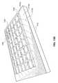
- FIG. 1Ais a perspective drawing illustrating an exemplary isotropic nanotube fabric layer
- FIG. 1Bis a perspective drawing illustrating an exemplary anisotropic nanotube fabric layer
- FIG. 2is a SEM image of an anisotropic nanotube fabric layer formed via the methods of the present disclosure
- FIG. 3Ais an illustration depicting a solution in an isotropic phase
- FIG. 3Bis an illustration depicting a solution in a nematic (or liquid crystalline) phase, according to one embodiment of the present disclosure
- FIG. 4is a graph plotting the Flory-Huggins parameter (X) against the concentration of a solution wherein the solute elements within said solution possess a length to diameter ratio (L/D) on the order of 100;
- FIG. 5is a simplified perspective drawing of a nanotube application system which includes a nozzle assembly, according to one embodiment of the present disclosure
- FIG. 6is a perspective drawing of an exemplary nanotube fabric formed via the nanotube application system of FIG. 5 ;
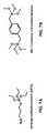
- FIG. 7Ais a chemical structure diagram of aminopropyltriethoxysilane (APTS).
- FIG. 7Bis a chemical structure diagram of bis (trimethoxy silyl methyl) benzene
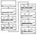
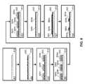
- FIG. 8is a fabrication process diagram illustrating a method of nanotube fabric formation using adhesion promoter materials, according to one embodiment of the present disclosure
- FIG. 9is a fabrication process diagram illustrating an air-liquid interface dip coating process, according to one embodiment of the present disclosure.
- FIG. 10is a fabrication process diagram illustrating a liquid-liquid interface dip coating process, according to one embodiment of the present disclosure.
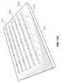
- FIG. 11is a fabrication process diagram illustrating a nanotube solution dip coating process, according to one embodiment of the present disclosure.
- FIGS. 12A-12Eare a series of SEM images (at increasing magnifications) of an anisotropic nanotube fabric layer formed via the methods of the present disclosure.
- FIGS. 13A-13Eare assembly diagrams depicting a touch screen device which includes isotropic nanotube fabric layers formed via the methods of the present disclosure.
- FIG. 1Aillustrates an isotropic nanotube fabric layer created with previously known methods (as discussed in detail within the incorporated references).
- a plurality of nanotube elements 110 aare dispersed randomly in a single layer over substrate element 120 a .
- the orientation (with respect to the plane of the nanotube fabric layer) of the individual nanotube elements 110 ais random, resulting in a plurality of gaps or voids 130 within the nanotube fabric layer.
- These gaps 130lead to non-uniform electrical characteristics across the nanotube fabric layer, and in some cases multiple layers are required to achieve desired electrical characteristics (such as, but not limited to, low sheet resistance and directional conductivity) within the nanotube fabric layer.
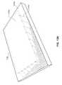
- FIG. 1Billustrates an anisotropic nanotube fabric layer formed via the methods of the present disclosure.
- a plurality of nanotube elements 110 bare distributed over substrate element 120 b such that substantially all of the individual nanotube elements 110 b are oriented in the same direction within the plane of the fabric layer, forming an anisotropic nanotube fabric.
- gap regions 130 present in the isotropic nanotube fabric layer depicted in FIG. 1Ahave been minimized in the anisotropic nanotube fabric depicted in FIG. 1B .
- FIG. 2is a TEM image of an anisotropic nanotube fabric layer formed via the methods of the present disclosure which corresponds to the exemplary fabric layer depicted in FIG. 1B .
- anisotropic nanotube fabricsare realized by using a nanotube application solution which has been rendered into a nematic (or liquid crystalline) phase.
- Flory-Huggins solution theorya mathematical model describing the thermodynamics of polymer solutions which is well known to those skilled in the art—teaches that for a solution comprising a substantially rigid (that is, inflexible) solute suspended within a solvent, said solution can be made to undergo a phase change from isotropic to nematic as the concentration of said solution is increased. That is, by increasing the volume density (or concentration) of a solute within a solvent, a solution may be rendered into a nematic phase.
- U.S. Pat. No. 7,375,369 to Sen et al.incorporated herein by reference in its entirety, teaches a nanotube application solution (that is, a volume of pristine nanotube elements suspended in a solvent) which is well suited to forming a nanotube fabric layer via a spin coating operation.
- the individual nanotube elements (the solute within the nanotube application solution) within such a solutionare rigid with a substantially large length to diameter ratio. Further, the concentration of nanotube elements within such a solution can be easily controlled (by introducing a plurality of additional individual nanotube elements, for example, or by removing a volume of the solvent).
- the concentration of such an application solutionthat is the volume density of nanotube elements suspended within the solvent liquid—can be manipulated such as to render the application solution into a nematic (or liquid crystalline) phase.
- This nematic application solutioncan then be applied to a substrate element via a spin coating process to fat it an anisotropic nanotube layer (as depicted in FIG. 1B and FIG. 2 ).
- FIGS. 3A-3Billustrate the technique (as taught by Flory-Huggins solution theory) of varying the concentration of an exemplary solution to realize a phase change within said solution from isotropic to nematic.
- the isotropic solution depicted in FIG. 3Ais comprised of a plurality of particles 310 a suspended within a solvent 320 a . It should be noted that the particles 310 a within the isotropic solution depicted in FIG. 3A show no uniformity in orientation.
- FIG. 3Billustrates an exemplary solution in a nematic (or liquid crystalline) phase. As in FIG. 3A , the solution depicted in FIG. 3B is comprised of a plurality of particles 310 b suspended within solvent 320 b . Within the solution depicted in FIG. 3B , the increased density of particles 310 b within the solvent 320 b has caused said particles 310 b to self align, rendering the solution into a nematic (or liquid crystalline) phase.
- the critical concentration of nanotube elements required to form a biphasic systemcan range from approximately 0.005 g/ml to approximately 0.05 g/ml, with a typical concentration being 0.01 g/ml.
- the concentration of nanotube elements in the solutionshould be increased from a level less than approximately 0.005 g/ml to a level greater than 0.05 g/ml.
- FIG. 4is a graph illustrating the phase change of an exemplary nanotube application solution as the concentration of said solution is varied.
- the individual nanotube elementsall possess a length to diameter ratio (L/D) of substantially 100.
- the graph depicted in FIG. 4plots the Flory-Huggins interaction parameter (X) against the concentration of said exemplary nanotube application solution in order to illustrate where a phase change (from isotropic to nematic) occurs.
- the Flory-Huggins interaction parameter (X)sometimes referred to as “the heat of mixing”—is well known to those skilled in the art and is a useful indicator within Flory-Huggins solution theory in describing phase changes of solutions.
- the graph depicted in FIG. 4shows three distinct regions: an isotropic region 410 , wherein said exemplary solution is rendered into an isotropic state; a nematic region 420 , wherein said exemplary solution is rendered into a nematic state; and a biphasic region 430 , where said exemplary solution is rendered in a mixed isotropic and nematic state.
- concentration of said exemplary solutionsuch that it remains within the nematic region 420 of the graph depicted in FIG. 4
- said exemplary solutionwill be rendered into a nematic phase.
- a fabric realized through a spin coat application of such a nematic solutionwill result in a substantially anisotropic nanotube fabric layer.
- FIG. 4illustrates a specific concentration range useful for rendering a specific exemplary nanotube application solution into a nematic phase
- the present inventionis not limited in this regard. Indeed, a graph such as is depicted in FIG. 4 is dependent on a plurality of parameters including, but not limited to, the L/D of the individual nanotube elements, the temperature of the solution, and the type of solvent used. It is preferred, therefore, that the methods of the present invention are not limited to this specific example presented.
- an anisotropic nanotube fabric layeris formed via flow induced alignment of individual nanotube elements.
- FIG. 5illustrates a simplified diagram of a nanotube application system which provides a method of forming an anisotropic nanotube fabric layer in a predetermined pattern over the surface of a substrate element.
- Supply tank 520contains a plurality of individual nanotube elements 510 suspended in an application solution.
- Pump structure 540draws said application solution (along with individual nanotube elements 510 ) up through intake tube 530 and provides same to nozzle structure 550 .
- individual nanotube elements 510flow through nozzle structure 550 , they are forced into a uniform orientation, substantially matching the orientation of nozzle structure 550 .
- individual nanotube elements 510are forced through nozzle structure 550 , said individual nanotube elements 510 are charged, for example by passing the nanotube elements 510 between charging plates 560 a and 560 b .
- the nanotube elements 510can be charged by any means known to one of skill in the art to charge nanotube elements.
- Individual nanotube elements 510exit nozzle assembly 550 at sufficient velocity as to pass between horizontal deflection plates 570 a and 570 b , vertical deflection plates 580 a and 580 b , and finally deposit themselves on substrate element 590 , forming nanotube fabric layer 595 .
- vertical and horizontal deflection platesare both shown in FIG.
- the nanotube elementscan be charged through either a horizontal or a vertical plate, or plates having any other alignment.
- nanotube fabric layer 595will tend to be anisotropic as all nanotube elements 510 deposited onto substrate element 590 will be oriented in substantially the same direction.
- a circular nozzlewould be employed.
- oval or slotted nozzleswould be employed.
- Electrode energycan provided (through additional circuitry not shown in FIG. 5 for the sake of clarity) to horizontal deflection plates 570 a and 570 b and vertical deflection plates 580 a and 580 b such as to provide electric fields of variable magnitude. These two electrical fields are used to deflect the charged individual nanotube elements 510 in the horizontal and vertical directions, respectively.
- an individual nanotube element 510can be deposited onto a specific point on substrate element 590 within a given radius without moving substrate element 590 or nozzle assembly 550 (this may be described as a “fine” targeting adjustment to the stream of nanotube elements 510 being applied to substrate element 590 ).
- substrate element 590can be moved in any direction orthogonal to nozzle assembly 550 (as shown in FIG. 5 ) in order to form anisotropic nanotube fabric layer 595 in a desired pattern (this may be described as a “coarse” targeting adjustment to the stream of nanotube elements 510 being applied to substrate element 590 ).
- deflection plates 570 a and 570 b or 580 a and 580 bare used to rotate the alignment of the nanotubes before deposition on the substrate, creating deposition that is no longer parallel to the nanotubes originating form nozzle 550 . This is accomplished by inducing a high electric field between the plates, which will rotate the alignment of the nanotubes from parallel to perpendicular.
- the substrate element 590may remain fixed in space and for the nozzle structure 550 (along with charging plates 560 a and 560 b , horizontal deflection plates 560 a and 560 b , and vertical deflection plates 580 a and 580 b ) to move to provide “coarse” targeting adjustments.
- charging plates 560 a and 560 b , horizontal charging plates 570 a and 570 b , and vertical charging plates 580 a and 580 bare not used. In such embodiments, no “fine” targeting adjustment to the stream of nanotube elements 510 is used.
- FIG. 6illustrates an exemplary anisotropic nanotube fabric formed via the nanotube application system depicted in FIG. 5 .
- Three shaped traces 610 a , 610 b , and 610 care formed over substrate element 620 .
- Each of the shaped traces 610 a , 610 b , and 610 cis an anisotropic nanotube fabric layer formed to a desired geometry and orientation without the need for patterning or etching techniques. In this way, highly conductive—and, in some embodiments, highly transparent—electrical traces can be formed rapidly over a substrate element.
- the nanotube fabric layercan be a single layer or a multilayer aligned fabric.
- Exemplary thicknesses of the single layer fabriccan range from about 50 nm to about 150 nm, while the multilayer fabric thicknesses can range from about 75 nm to about 200 nm.
- anisotropic nanotube fabric layersare realized using adhesion promoter materials formed into narrow strips over a substrate.
- FIG. 7Adepicts the structural chemical diagram of aminopropyltriethoxysilane (APTS), a material which promotes the adhesion of carbon nanotube elements.
- APTSaminopropyltriethoxysilane
- FIG. 7Adepicts the structural chemical diagram of aminopropyltriethoxysilane (APTS), a material which promotes the adhesion of carbon nanotube elements.
- APTSis comprised of two groups: an oxysilane group which adheres readily to a silicon wafer (as would be used in a standard semiconductor fabrication process); and an amino group (H 2 N—) which adheres readily to carbon nanotube elements.
- a layer of APTSmay be applied in a desired pattern over a substrate element and used to form an anisotropic nanotube fabric layer.
- FIG. 7Bdepicts the structural chemical diagram of bis (trimethoxy silyl methyl) benzene, which tends to avert the adhesion of carbon nanotube elements.
- bis (trimethoxy silyl methyl) benzenecomprises a pair of oxysilane groups which adhere readily to silicon wafers. However the remaining group—the benzene ring—does not readily adhere to carbon nanotube elements.
- a layer of bis (trimethoxy silyl methyl) benzenecan be formed over a substrate element and used to prevent the formation of a nanotube fabric layer.
- adhesion promotersfor carbon nanotubes functionalized with —COOH groups in an aqueous medium three classes of surface modifiers can be used as adhesion promoters: protic basic (which promote adhesion due to interaction with the acidic groups on carbon nanotubes), aprotic basic, and polar aprotic.
- adhesion promoter materialswhich are well suited for use as adhesion promoters as taught by the present disclosure. It should be noted that the following list is not inclusive of all adhesion promoter materials suitable for use with the methods of the present disclosure. Indeed, the following list is intended only to provide a non-limiting list of exemplary adhesion promoter materials:
- adhesion averter materialswhich are well suited for use as adhesion averters as taught by the present disclosure. It should be noted that the following list is not inclusive of all adhesion averter materials suitable for use with the methods of the present disclosure. Indeed, the following list is intended only to provide a non-limiting list of exemplary adhesion averter materials:
- FIG. 8is a fabrication process diagram illustrating a method of forming anisotropic nanotube fabric layers using a combination of a nanotube adhesion promoter material—such as, but not limited to, APTS—and a nanotube adhesion averter material—such as, but not limited to, bis (trimethoxy silyl methyl) benzene to form a patterned application surface.
- a nanotube adhesion promoter materialsuch as, but not limited to, APTS
- a nanotube adhesion averter materialsuch as, but not limited to, bis (trimethoxy silyl methyl) benzene
- first process step 801a substrate element 810 is provided.
- a self assembled monolayer of a nanotube adhesion averter material 820such as, but not limited to, bis (trimethoxy silyl methyl) benzene—is deposited over substrate element 810 .
- photoresist blocks 830 a , 830 b , and 830 care deposited in a predetermined pattern over nanotube adhesion averter material monolayer 820 .
- an etch processsuch as, but not limited to, an oxygen plasma etch process—is used to remove those areas of nanotube adhesion averter material monolayer 820 not covered by photoresist blocks 830 a , 830 b , and 830 c , foaming gaps 820 a and 820 b .
- gaps 820 a and 820 bare backfilled with an adhesion promoter material—such as, but not limited to, APTS—to form nanotube adhesion structures 840 a and 840 b .
- an adhesion promoter materialsuch as, but not limited to, APTS
- a layer of nanotube elements 850is deposited over the surface of the patterned application surface formed by nanotube adhesion averter material monolayer 820 and nanotube adhesion structures 840 a and 840 b .
- the nanotube elementsare applied through a spray coating method described in FIG. 5 .
- a dip coating processcan be used to apply the nanotube fabric layer.
- FIGS. 9 , 10 , and 11illustrate exemplary dip coating processes suitable for applying the nanotube fabric layer 850 .
- An exemplary dip coating processeswill be described in detail in the discussion of those figures below. However, it should be noted that the methods of this aspect of the present disclosure are not limited to a dip coating process.
- a plurality of other application methodscould be employed to apply nanotube fabric layer 850 over the patterned application surface formed by nanotube adhesion averter material monolayer 820 and nanotube adhesion structures 840 a and 840 b .
- Such other application methodsinclude, but are not limited to, spin coating and spray coating.
- an eighth and final process step 808the entire assembly is washed and dried leaving nanotube fabric layers 850 a and 850 b over nanotube adhesion structures 840 a and 840 b only.
- the nanotube material deposited over nanotube adhesion averter material monolayer 820is removed during the wash process as the nanotube material does not adhere to the monolayer 820 .
- the individual nanotube elements within nanotube fabric layers 850 a and 850 bwill tend to self align and form anisotropic nanotube fabric layers as said individual nanotube elements are confined to only the regions of the patterned application surface containing the nanotube adhesion promoter material.
- the nanotube adhesion structurescan be about 1 nm to about 10 nm in width.
- the use of a carefully controlled dip coating processcan also aid in the creation of these anisotropic nanotube fabric layers.
- parameters for the dip coating processinginclude room temperature, a volume density in solution that correlates to between about an optical density of about 2.0 and dip coating pull rates of about 5.4 microns/second to about 54 microns/second.
- the fabric layerscan be a single or multiple layer aligned nanotube fabric, having thicknesses ranging from about 50 nm to about 200 nm.
- substrate element 810as a silicon wafer (as would be typical in a semiconductor fabrication process), it should be noted that the methods of the present disclosure are not limited in this regard. Indeed, substrate element 810 could be formed from a plurality of materials including, but not limited to, semiconductors, plastic, transparent materials such as glass, optical glass, and quartz, indium-tin oxide films, and flexible polymeric/plastic substrates such as polyethylene terephthalate (PET), polyolefins, and polycarbonate. Further, the substrate can be a flexible substrate.
- the nanotube fabriccan be applied to a flexible substrate and the nanotube fabric can bend and flex with the flexible substrate without negatively affecting the performance or the operative lifetime of the nanotube fabric.
- the fabrication method described in FIG. 8and specifically the technique of using a nanotube adhesion promoter material such as APTS—allows for the formation of nanotube fabric layers (both anisotropic and isotropic) over a plurality of surfaces which do not readily adhere to nanotube fabrics alone.
- FIGS. 12A-12Eare a series of SEM images (at increasing magnifications) of an anisotropic nanotube fabric layer formed via the fabrication method depicted in FIG. 8 and described in detail in the discussion of that figure.
- dark regions 1210are narrow anisotropic nanotube fabric layers corresponding to anisotropic nanotube fabric layers 850 a and 850 b in FIG. 8 .
- the wider light regions 1220contain substantially no nanotube elements and correspond to nanotube adhesion averter material 820 in FIG. 8 .
- FIG. 12Bwhich increases the magnification of the structure depicted in FIG. 12A by a factor of twenty, provides a close up view of a single narrow anisotropic nanotube fabric layer 1210 a .
- the individual nanotube elements within anisotropic nanotube fabric layer 1210 ajust begin to resolve into view, and the absence of such nanotube elements on the nanotube adhesion averter material 1220 is evident.
- FIG. 12Cincreases the magnification of the structure depicted in FIG. 12B by a factor of 2.5
- FIG. 12Dincreases the magnification of the structure depicted in FIG. 12B by a factor of 5
- FIG. 12Eincreases the magnification of the structure depicted in FIG. 12B by a factor of 10.
- FIG. 9illustrates an air-liquid interface dip coating process suitable for use within the fabrication process illustrated in FIG. 8 and discussed in detail above.
- a first process step 901a plurality of nanotube elements 920 are deposited over the surface of a liquid 930 .
- Substrate assembly 910comprising substrate element 910 a (which corresponds to substrate element 810 in FIG. 8 ) and patterned nanotube application layer 910 b —is suspended above liquid 930 .
- the apparatus used to suspend—and, in subsequent process steps, lower and raise—substrate assembly 910is not shown in FIG. 9 for the sake of clarity.
- a guide apparatus 950is positioned within the liquid 930 and, in subsequent process steps, is used to guide individual nanotube elements 920 toward and onto substrate assembly 910 .
- a second process step 902substrate assembly 910 is lowered into liquid 930 and guide apparatus 950 is used to compress the individual nanotube elements 920 floating over the surface of liquid 930 against the patterned nanotube application layer 910 b .
- substrate assembly 910is raised up from liquid 930 while guide apparatus 950 is simultaneously moved forward to continuously guide individual nanotube elements 920 toward and onto patterned nanotube application layer 910 b .
- substrate assembly 910is raised completely out of liquid 930 , and an anisotropic nanotube fabric layer has been formed on the portion of substrate assembly 910 which was submerged within liquid 930 .
- this anisotropic nanotube fabric layerwill be dependant on a plurality of factors—such as, but not limited to, the speed of the dip coating process, the concentration of nanotube elements 920 floating on the surface of the liquid 930 , and the materiel used to form patterned nanotube application layer 910 b —in some embodiments, for example, the thickness of this anisotropic nanotube fabric layer can range from 1 nm to 1000 nm with some thicknesses ranging between about 50 nm to about 200 nm.
- FIG. 10illustrates a liquid-liquid interface dip coating process suitable for use within the fabrication process illustrated in FIG. 8 and discussed in detail above.
- a first process step 1001a plurality of nanotube elements 1020 are deposited over the surface of a first liquid 1030 and a second liquid 1040 is deposited over said plurality of nanotube elements 1020 .
- the relative densities of the first liquid 1030 and the second liquid 1040are such that the plurality of nanotube elements 1020 remain compressed between them.
- substrate assembly 1010comprising substrate element 1010 a (which corresponds to substrate element 810 in FIG. 8 ) and patterned nanotube application layer 1010 b —is suspended above second liquid 1040 .
- the apparatus used to suspend—and, in subsequent process steps, lower and raise—substrate assembly 1010is not shown in FIG. 10 for the sake of clarity.
- a guide apparatus 1050is positioned within the second liquid 1040 , extending partially into first liquid 1030 . In subsequent process steps, guide apparatus 1050 is used to guide individual nanotube elements 1020 toward and onto substrate assembly 1010 .
- substrate assembly 1010is lowered into both first liquid 1030 and second liquid 1040 .
- Guide apparatus 1050is used to compress the individual nanotube elements 1020 compressed between first liquid 1030 and second liquid 1040 against the patterned nanotube application layer 1010 b .
- substrate assembly 1010is raised up while guide apparatus 1050 is simultaneously moved forward to continuously guide individual nanotube elements 1020 toward and onto patterned nanotube application layer 1010 b .
- substrate assembly 1010is raised completely out of first liquid 1030 and second liquid 1040 , and an anisotropic nanotube fabric layer has been formed on the portion of substrate assembly 1010 which was submerged within first liquid 1030 .
- this anisotropic nanotube fabric layerwill be dependant on a plurality of factors—such as, but not limited to, the speed of the dip coating process, the concentration of nanotube elements 1020 compressed between first liquid 1030 and second liquid 1040 , and the materiel used to form patterned nanotube application layer 1010 b —in some embodiments, for example, the thickness of this anisotropic nanotube fabric layer can range from 1 nm to 1000 nm with some thicknesses ranging between about 50 nm to about 200 nm.
- FIG. 11illustrates a dip coating process using a nanotube solution suitable for use within the fabrication process illustrated in FIG. 8 and discussed in detail above.
- a first process step 1101a plurality of nanotube elements 1120 are suspended in nanotube solution 1130 (such nanotube solutions are described in detail within U.S. Pat. No. 7,375,369 to Sen et al., incorporated herein by reference in its entirety).
- Substrate assembly 1110comprising substrate element 1110 a (which corresponds to substrate element 810 in FIG. 8 ) and patterned nanotube application layer 1110 b —is suspended above nanotube solution 1130 .
- the apparatus used to suspend—and, in subsequent process steps, lower and raise—substrate assembly 1110is not shown in FIG. 11 for the sake of clarity.
- substrate assembly 1110is lowered into nanotube application solution 1130 and the individual nanotube elements 1120 suspended within nanotube application solution 1130 are allowed to come into physical contact with patterned nanotube application layer 1110 b .
- substrate assembly 1110is raised completely out of nanotube application solution 1130 , and an anisotropic nanotube fabric layer has been formed on the portion of substrate assembly 1110 which was submerged within nanotube application solution 1130 .
- this anisotropic nanotube fabric layerwill be dependant on a plurality of factors—such as, but not limited to, the speed of the dip coating process, the concentration of nanotube elements 1120 within nanotube application solution 1130 , and the materiel used to form patterned nanotube application layer 1110 b —in some embodiments, for example, the thickness of this anisotropic nanotube fabric layer can range from 1 nm to 1000 nm with some thicknesses ranging between about 50 nm to about 200 nm.
- FIGS. 13A-13Eare assembly diagrams illustrating a touch screen device which includes a plurality of thin anisotropic nanotube fabric layers formed via the methods of the present disclosure.
- an electronic device assembly 1310includes display screen element 1310 a , electronics housing 1310 b , and a plurality of conductive traces along the surface of electronics housing 1310 b which provide contact points at evenly spaced intervals along two edges of display screen element 1310 a .
- Electronic device assembly 1310is intended to be an exemplary electronic device which is well known to those skilled in the art. Indeed, the base electronics assemblies for a plurality of commercial products such as, but not limited to, cellular telephones, commercial navigation systems, and electronic book readers are well represented by the simplified structure depicted as electronic device assembly 1310 .
- a plurality of horizontally oriented anisotropic nanotube fabric articles 1320are deposited over display screen element 1310 a such that each horizontally oriented nanotube fabric article 1320 makes electrical contact with a trace element 1310 c .
- the present disclosurepresents a plurality of methods for depositing such anisotropic nanotube fabric articles over a substrate element such as glass or plastic which would be used to form display screen element 1310 a . Such methods are depicted in previous figures and discussed in detail above.
- a transparent dielectric layer 1330is deposited over horizontally oriented anisotropic nanotube fabric articles 1320 , providing a new substrate surface above—and electrically isolated from—horizontally oriented nanotube fabric articles 1320 .
- a plurality of vertically oriented anisotropic nanotube fabric articles 1340are deposited over transparent dielectric layer 1330 such that each nanotube fabric article 1340 makes electrical contact with a trace element 1310 c .
- FIG. 13Eprovides an exploded view of the entire assembly.
- horizontally oriented nanotube fabric articles 1320 and vertically oriented nanotube fabric articles 1340may be kept relatively thin while still remaining sufficiently conductive. This allows for both sets of fabric articles 1320 and 1340 to remain highly transparent and not impede the function of display screen element 1310 a . In this way, a plurality of narrow anisotropic nanotube fabric articles (horizontally oriented nanotube fabric articles 1320 and vertically oriented nanotube fabric articles 1340 ) are used to create a plurality of cross point capacitive switch elements, which can be used to provide a transparent touch screen interface over display screen element 1310 a.
- FIGS. 13D-13Eare not necessarily to scale, but have been drawn simply to imply the anisotropic nature of the nanotube fabric articles 1320 and 1340 .
Landscapes
- Engineering & Computer Science (AREA)
- Chemical & Material Sciences (AREA)
- Nanotechnology (AREA)
- Manufacturing & Machinery (AREA)
- Materials Engineering (AREA)
- Condensed Matter Physics & Semiconductors (AREA)
- General Physics & Mathematics (AREA)
- Physics & Mathematics (AREA)
- Crystallography & Structural Chemistry (AREA)
- Microelectronics & Electronic Packaging (AREA)
- Organic Chemistry (AREA)
- Composite Materials (AREA)
- Inorganic Chemistry (AREA)
- Application Of Or Painting With Fluid Materials (AREA)
- Carbon And Carbon Compounds (AREA)
Abstract
Description
c=3.3ρD/L
- ρ=the density of said rigid rod elements
- D=the diameter of said rigid rod elements
- L=the length of the said rod elements
- ρ=˜1.75 g/ml
- D=1-2 nm
- L=200 nm-1000 nm
- Protic Basic Promoters:
- 3-aminopropyl triethoxy silane (APTS)
- Bis(3-trimethoxysilylpropyl)amine
- Bis(2-hydroxyethyl)-3-aminopropyl-triethoxysilane
- N-butylaminopropyl trimetohoxysilane
- Aprotic Basic Promoters:
- 3-(N,N-diemethylaminopropyl)-trimethoxysilane
- N-n-bulty-aza-2,2-dimethoxysilacyclopentane
- Polar Aprotic Promoters:
- acetoxypropyltrimethoxysilane
- (N-acetylglycyl)-3-aminopropyl trimethoxy silane
- Benzoyloxypropyl trimethoxy silane
- Protic Basic Promoters:
- bis (trimethoxy silyl ethyl) benzene
- Hexamethyl disilazane (HMDS)
- octadecyl trichlorosilane (OTS)
Claims (24)
Priority Applications (3)
| Application Number | Priority Date | Filing Date | Title |
|---|---|---|---|
| US12/533,695US8128993B2 (en) | 2009-07-31 | 2009-07-31 | Anisotropic nanotube fabric layers and films and methods of forming same |
| PCT/US2010/043207WO2011014446A1 (en) | 2009-07-31 | 2010-07-26 | Anisotropic nanotube fabric layers and films and methods of forming same |
| TW099125228ATWI544520B (en) | 2009-07-31 | 2010-07-30 | Anisotropic nanotube fabric layers and films and methods of forming same |
Applications Claiming Priority (1)
| Application Number | Priority Date | Filing Date | Title |
|---|---|---|---|
| US12/533,695US8128993B2 (en) | 2009-07-31 | 2009-07-31 | Anisotropic nanotube fabric layers and films and methods of forming same |
Publications (2)
| Publication Number | Publication Date |
|---|---|
| US20110027497A1 US20110027497A1 (en) | 2011-02-03 |
| US8128993B2true US8128993B2 (en) | 2012-03-06 |
Family
ID=43527295
Family Applications (1)
| Application Number | Title | Priority Date | Filing Date |
|---|---|---|---|
| US12/533,695Active2030-03-11US8128993B2 (en) | 2009-07-31 | 2009-07-31 | Anisotropic nanotube fabric layers and films and methods of forming same |
Country Status (1)
| Country | Link |
|---|---|
| US (1) | US8128993B2 (en) |
Cited By (2)
| Publication number | Priority date | Publication date | Assignee | Title |
|---|---|---|---|---|
| US9786853B2 (en) | 2014-02-11 | 2017-10-10 | Wisconsin Alumni Research Foundation | Floating evaporative assembly of aligned carbon nanotubes |
| US10873026B2 (en) | 2017-03-10 | 2020-12-22 | Wisconsin Alumni Research Foundation | Alignment of carbon nanotubes in confined channels |
Families Citing this family (4)
| Publication number | Priority date | Publication date | Assignee | Title |
|---|---|---|---|---|
| SG11201408561YA (en)* | 2012-06-21 | 2015-01-29 | Tesla Nanocoatings Inc | Tunable materials |
| US9635875B2 (en) | 2013-05-30 | 2017-05-02 | Burcon Nutrascience (Mb) Corp. | Production of pulse protein products with reduced astringency |
| US9879141B2 (en) | 2014-12-19 | 2018-01-30 | Tesla Nanocoatings, Inc. | Tunable materials |
| WO2020233809A1 (en)* | 2019-05-22 | 2020-11-26 | Toyota Motor Europe | Solution-based deposition method for preparing semiconducting thin films via dispersed particle self-assembly at a liquid-liquid interface |
Citations (110)
| Publication number | Priority date | Publication date | Assignee | Title |
|---|---|---|---|---|
| EP0947466A1 (en) | 1997-03-21 | 1999-10-06 | Japan Fine Ceramics Center | Process for producing carbon nanotubes, process for producing carbon nanotube film, and structure provided with carbon nanotube film |
| US6057637A (en) | 1996-09-13 | 2000-05-02 | The Regents Of The University Of California | Field emission electron source |
| JP2000203821A (en) | 1999-01-18 | 2000-07-25 | Toshiyuki Tsuboi | Method for forming film of carbon nanotube, carbon nanotube film formed by the method and electric field electron release source using the same |
| EP1061040A1 (en) | 1999-06-15 | 2000-12-20 | Iljin Nanotech Co., Ltd. | Mass purification method of carbon nanotubes |
| US6187823B1 (en) | 1998-10-02 | 2001-02-13 | University Of Kentucky Research Foundation | Solubilizing single-walled carbon nanotubes by direct reaction with amines and alkylaryl amines |
| US20010004979A1 (en) | 1999-12-14 | 2001-06-28 | Lg Electronics Inc. | Field emission display and method for fabricating the same |
| US6277318B1 (en) | 1999-08-18 | 2001-08-21 | Agere Systems Guardian Corp. | Method for fabrication of patterned carbon nanotube films |
| US6331262B1 (en) | 1998-10-02 | 2001-12-18 | University Of Kentucky Research Foundation | Method of solubilizing shortened single-walled carbon nanotubes in organic solutions |
| US6342276B1 (en) | 1999-12-10 | 2002-01-29 | Samsung Sdi Co., Ltd. | Method for making a field emission display |
| GB2364933A (en) | 2000-07-18 | 2002-02-13 | Lg Electronics Inc | Method of horizontally growing carbon nanotubes and field effect transistor using the carbon nanotubes grown by the method |
| US6368569B1 (en) | 1998-10-02 | 2002-04-09 | University Of Kentucky Research Foundation | Method of solubilizing unshortened carbon nanotubes in organic solutions |
| US6409567B1 (en) | 1997-12-15 | 2002-06-25 | E.I. Du Pont De Nemours And Company | Past-deposited carbon electron emitters |
| US20020081380A1 (en) | 1999-08-12 | 2002-06-27 | Dillon Anne C. | Highly purified single-wall carbon nanotubes and production thereof |
| US6422450B1 (en) | 1999-03-01 | 2002-07-23 | University Of North Carolina, The Chapel | Nanotube-based high energy material and method |
| US6423583B1 (en) | 2001-01-03 | 2002-07-23 | International Business Machines Corporation | Methodology for electrically induced selective breakdown of nanotubes |
| US20020160111A1 (en) | 2001-04-25 | 2002-10-31 | Yi Sun | Method for fabrication of field emission devices using carbon nanotube film as a cathode |
| US20020175390A1 (en) | 2001-04-03 | 2002-11-28 | Goldstein Seth Copen | Electronic circuit device, system, and method |
| US6495258B1 (en) | 2000-09-20 | 2002-12-17 | Auburn University | Structures with high number density of carbon nanotubes and 3-dimensional distribution |
| US6495116B1 (en) | 2000-04-10 | 2002-12-17 | Lockheed Martin Corporation | Net shape manufacturing using carbon nanotubes |
| US20030004058A1 (en) | 2001-05-21 | 2003-01-02 | Trustees Of Boston College | Varied morphology carbon nanotubes and method for their manufacture |
| US20030012723A1 (en)* | 2001-07-10 | 2003-01-16 | Clarke Mark S.F. | Spatial localization of dispersed single walled carbon nanotubes into useful structures |
| US20030017560A1 (en)* | 2000-09-04 | 2003-01-23 | Chih-Wei Ho | High-density functional slide and preparation method thereof |
| US6528020B1 (en) | 1998-08-14 | 2003-03-04 | The Board Of Trustees Of The Leland Stanford Junior University | Carbon nanotube devices |
| US6531513B2 (en) | 1998-10-02 | 2003-03-11 | University Of Kentucky Research Foundation | Method of solubilizing carbon nanotubes in organic solutions |
| US20030065206A1 (en) | 2001-10-01 | 2003-04-03 | Bolskar Robert D. | Derivatization and solubilization of insoluble classes of fullerenes |
| US20030122111A1 (en) | 2001-03-26 | 2003-07-03 | Glatkowski Paul J. | Coatings comprising carbon nanotubes and methods for forming same |
| US20030177450A1 (en) | 2002-03-12 | 2003-09-18 | Alex Nugent | Physical neural network design incorporating nanotechnology |
| US20030178617A1 (en)* | 2002-03-20 | 2003-09-25 | International Business Machines Corporation | Self-aligned nanotube field effect transistor and method of fabricating same |
| US6630772B1 (en) | 1998-09-21 | 2003-10-07 | Agere Systems Inc. | Device comprising carbon nanotube field emitter structure and process for forming device |
| US20030200521A1 (en) | 2002-01-18 | 2003-10-23 | California Institute Of Technology | Array-based architecture for molecular electronics |
| US6641793B2 (en) | 1998-10-02 | 2003-11-04 | University Of Kentucky Research Foundation | Method of solubilizing single-walled carbon nanotubes in organic solutions |
| US6645628B2 (en) | 2001-11-13 | 2003-11-11 | The United States Of America As Represented By The Secretary Of The Air Force | Carbon nanotube coated anode |
| US20030220518A1 (en) | 2001-10-01 | 2003-11-27 | Bolskar Robert D. | Derivatization and solubilization of fullerenes for use in therapeutic and diagnostic applications |
| US20040005723A1 (en) | 2002-04-02 | 2004-01-08 | Nanosys, Inc. | Methods of making, positioning and orienting nanostructures, nanostructure arrays and nanostructure devices |
| US20040007528A1 (en) | 2002-07-03 | 2004-01-15 | The Regents Of The University Of California | Intertwined, free-standing carbon nanotube mesh for use as separation, concentration, and/or filtration medium |
| US20040023253A1 (en) | 2001-06-11 | 2004-02-05 | Sandeep Kunwar | Device structure for closely spaced electrodes |
| US20040023514A1 (en) | 2002-08-01 | 2004-02-05 | Semiconductor Energy Laboratory Co., Ltd. | Method of manufacturing carbon nonotube semiconductor device |
| US20040034177A1 (en) | 2002-05-02 | 2004-02-19 | Jian Chen | Polymer and method for using the polymer for solubilizing nanotubes |
| US20040031975A1 (en) | 2002-03-18 | 2004-02-19 | Max-Planck-Gesellschaft Zur Forderung Der Wissenschaften E.V., A German Corporation | Field effect transistor memory cell, memory device and method for manufacturing a field effect transistor memory cell |
| US20040043527A1 (en) | 2002-09-04 | 2004-03-04 | Nanomix, Inc. | Sensitivity control for nanotube sensors |
| US20040041154A1 (en) | 2002-09-04 | 2004-03-04 | Fuji Xerox Co., Ltd. | Electric part and method of manufacturing the same |
| US6707098B2 (en) | 2000-07-04 | 2004-03-16 | Infineon Technologies, Ag | Electronic device and method for fabricating an electronic device |
| US6706402B2 (en) | 2001-07-25 | 2004-03-16 | Nantero, Inc. | Nanotube films and articles |
| US20040071949A1 (en) | 2001-07-27 | 2004-04-15 | Glatkowski Paul J. | Conformal coatings comprising carbon nanotubes |
| WO2004039893A1 (en) | 2002-11-01 | 2004-05-13 | Mitsubishi Rayon Co., Ltd. | Composition containing carbon nanotubes, composite having coating thereof and process for producing them |
| US20040099438A1 (en) | 2002-05-21 | 2004-05-27 | Arthur David J. | Method for patterning carbon nanotube coating and carbon nanotube wiring |
| US20040104129A1 (en) | 2002-11-27 | 2004-06-03 | Gang Gu | Nanotube chemical sensor based on work function of electrodes |
| US20040106741A1 (en)* | 2002-09-17 | 2004-06-03 | Kriesel Joshua W. | Nanofilm compositions with polymeric components |
| US6752977B2 (en) | 2001-02-12 | 2004-06-22 | William Marsh Rice University | Process for purifying single-wall carbon nanotubes and compositions thereof |
| US20040132070A1 (en) | 2002-01-16 | 2004-07-08 | Nanomix, Inc. | Nonotube-based electronic detection of biological molecules |
| WO2004065671A1 (en) | 2003-01-13 | 2004-08-05 | Nantero, Inc. | Carbon nanotube films, layers, fabrics, ribbons, elements and articles |
| WO2004065657A1 (en) | 2003-01-13 | 2004-08-05 | Nantero, Inc. | Methods of making carbon nanotube films, layers, fabrics, ribbons, elements and articles |
| WO2004065655A1 (en) | 2003-01-13 | 2004-08-05 | Nantero, Inc. | Methods of using thin metal layers to make carbon nanotube films, layers, fabrics, ribbons, elements and articles |
| US20040181630A1 (en) | 2001-07-25 | 2004-09-16 | Nantero, Inc. | Devices having horizontally-disposed nanofabric articles and methods of making the same |
| US6808746B1 (en) | 1999-04-16 | 2004-10-26 | Commonwealth Scientific and Industrial Research Organisation Campell | Multilayer carbon nanotube films and method of making the same |
| US20040253167A1 (en) | 2001-07-27 | 2004-12-16 | Silva Sembukutiarachilage Ravi | Production of carbon nanotubes |
| US6833558B2 (en) | 2000-08-23 | 2004-12-21 | Korea Institute Of Science And Technology | Parallel and selective growth method of carbon nanotube on the substrates for electronic-spintronic device applications |
| US20040265550A1 (en) | 2002-12-06 | 2004-12-30 | Glatkowski Paul J. | Optically transparent nanostructured electrical conductors |
| US20040266106A1 (en) | 2003-06-30 | 2004-12-30 | Hynix Semiconductor Inc. | Method for forming bit line of flash device |
| US6858197B1 (en) | 2002-03-13 | 2005-02-22 | The United States Of America As Represented By The Administrator Of The National Aeronautics And Space Administration | Controlled patterning and growth of single wall and multi-wall carbon nanotubes |
| US6863942B2 (en) | 1998-06-19 | 2005-03-08 | The Research Foundation Of State University Of New York | Free-standing and aligned carbon nanotubes and synthesis thereof |
| US20050053525A1 (en) | 2003-05-14 | 2005-03-10 | Nantero, Inc. | Sensor platform using a horizontally oriented nanotube element |
| US20050058797A1 (en) | 2003-09-08 | 2005-03-17 | Nantero, Inc. | High purity nanotube fabrics and films |
| US6888773B2 (en) | 2002-12-05 | 2005-05-03 | Sharp Kabushiki Kaisha | Semiconductor memory device and erase method for memory array |
| US20050095938A1 (en) | 2003-10-29 | 2005-05-05 | Rosenberger Brian T. | Carbon nanotube fabrics |
| US6890780B2 (en) | 2003-10-10 | 2005-05-10 | General Electric Company | Method for forming an electrostatically-doped carbon nanotube device |
| US20050101112A1 (en) | 2001-07-25 | 2005-05-12 | Nantero, Inc. | Methods of nanotubes films and articles |
| US6899945B2 (en) | 2002-03-19 | 2005-05-31 | William Marsh Rice University | Entangled single-wall carbon nanotube solid material and methods for making same |
| US6905892B2 (en) | 2001-07-20 | 2005-06-14 | Infineon Technologies Ag | Operating method for a semiconductor component |
| US20050142281A1 (en)* | 2003-12-24 | 2005-06-30 | Molaire Michel F. | Dip coating process for producing electrophotographic composition layer having controlled thickness |
| US6918284B2 (en) | 2003-03-24 | 2005-07-19 | The United States Of America As Represented By The Secretary Of The Navy | Interconnected networks of single-walled carbon nanotubes |
| US6919740B2 (en) | 2003-01-31 | 2005-07-19 | Hewlett-Packard Development Company, Lp. | Molecular-junction-nanowire-crossbar-based inverter, latch, and flip-flop circuits, and more complex circuits composed, in part, from molecular-junction-nanowire-crossbar-based inverter, latch, and flip-flop circuits |
| US6919592B2 (en) | 2001-07-25 | 2005-07-19 | Nantero, Inc. | Electromechanical memory array using nanotube ribbons and method for making same |
| US6921575B2 (en) | 2001-05-21 | 2005-07-26 | Fuji Xerox Co., Ltd. | Carbon nanotube structures, carbon nanotube devices using the same and method for manufacturing carbon nanotube structures |
| US6924538B2 (en) | 2001-07-25 | 2005-08-02 | Nantero, Inc. | Devices having vertically-disposed nanofabric articles and methods of making the same |
| US6946410B2 (en) | 2002-04-05 | 2005-09-20 | E. I. Du Pont De Nemours And Company | Method for providing nano-structures of uniform length |
| US20050212014A1 (en) | 2004-03-26 | 2005-09-29 | Masahiro Horibe | Semiconductor device and semiconductor sensor |
| US20050269554A1 (en) | 2004-06-03 | 2005-12-08 | Nantero, Inc. | Applicator liquid containing ethyl lactate for preparation of nanotube films |
| US7015500B2 (en) | 2002-02-09 | 2006-03-21 | Samsung Electronics Co., Ltd. | Memory device utilizing carbon nanotubes |
| US7057402B2 (en) | 2002-03-18 | 2006-06-06 | Honeywell International Inc. | Carbon nanotube sensor |
| WO2006078293A2 (en) | 2004-06-03 | 2006-07-27 | Nantero, Inc. | Method of making an applicator liquid for electronics fabrication process |
| US20060204427A1 (en) | 2004-12-16 | 2006-09-14 | Nantero, Inc. | Aqueous carbon nanotube applicator liquids and methods for producing applicator liquids thereof |
| US7115864B2 (en) | 1996-08-08 | 2006-10-03 | William Marsh Rice University | Method for purification of as-produced single-wall carbon nanotubes |
| US20060237537A1 (en) | 2002-09-30 | 2006-10-26 | Nanosys, Inc. | Applications of nano-enabled large area macroelectronic substrates incorporating nanowires and nanowire composites |
| US20060250843A1 (en) | 2005-05-09 | 2006-11-09 | Nantero, Inc. | Non-volatile-shadow latch using a nanotube switch |
| US20060250856A1 (en) | 2005-05-09 | 2006-11-09 | Nantero, Inc. | Memory arrays using nanotube articles with reprogrammable resistance |
| US20060258122A1 (en) | 2005-05-12 | 2006-11-16 | Whitefield Bruce J | Nanotube fuse structure |
| US20060264053A1 (en) | 2005-05-23 | 2006-11-23 | Lsi Logic Corporation | Method of aligning nanotubes and wires with an etched feature |
| US20060276056A1 (en) | 2005-04-05 | 2006-12-07 | Nantero, Inc. | Nanotube articles with adjustable electrical conductivity and methods of making the same |
| US20060281287A1 (en) | 2005-06-09 | 2006-12-14 | Yates Colin D | Method of aligning deposited nanotubes onto an etched feature using a spacer |
| US20060281306A1 (en)* | 2005-06-08 | 2006-12-14 | Florian Gstrein | Carbon nanotube interconnect contacts |
| US20060281256A1 (en) | 2005-06-08 | 2006-12-14 | Carter Richard J | Self-aligned cell integration scheme |
| US20060292716A1 (en) | 2005-06-27 | 2006-12-28 | Lsi Logic Corporation | Use selective growth metallization to improve electrical connection between carbon nanotubes and electrodes |
| US20070004191A1 (en) | 2005-06-30 | 2007-01-04 | Lsi Logic Corporation | Novel techniques for precision pattern transfer of carbon nanotubes from photo mask to wafers |
| US7161403B2 (en) | 2004-06-18 | 2007-01-09 | Nantero, Inc. | Storage elements using nanotube switching elements |
| US20070014979A1 (en)* | 2005-07-15 | 2007-01-18 | Aspen Aerogels, Inc. | Secured Aerogel Composites and Methods of Manufacture Thereof |
| US7365632B2 (en) | 2004-09-21 | 2008-04-29 | Nantero, Inc. | Resistive elements using carbon nanotubes |
| US7375369B2 (en) | 2003-09-08 | 2008-05-20 | Nantero, Inc. | Spin-coatable liquid for formation of high purity nanotube films |
| US20080157126A1 (en) | 2005-05-09 | 2008-07-03 | Nantero, Inc. | Nonvolatile nanotube diodes and nonvolatile nanotube blocks and systems using same and methods of making same |
| US20080159042A1 (en) | 2005-05-09 | 2008-07-03 | Bertin Claude L | Latch circuits and operation circuits having scalable nonvolatile nanotube switches as electronic fuse replacement elements |
| US20080170429A1 (en) | 2005-05-09 | 2008-07-17 | Nantero, Inc. | Nonvolatile nanotube diodes and nonvolatile nanotube blocks and systems using same and methods of making same |
| US20080207581A1 (en) | 2005-12-12 | 2008-08-28 | Allaccem, Inc. | Methods and systems for coating a surface |
| US20090020924A1 (en) | 2007-02-21 | 2009-01-22 | Iowa State University Research Foundation, Inc. | Drying-mediated self-assembly of ordered or hierarchically ordered micro- and sub-micro scale structures and their uses as multifunctional materials |
| US20090095412A1 (en) | 2007-05-30 | 2009-04-16 | Ramot At Tel Aviv University Ltd. | Nanotube network and method of fabricating the same |
| US7566478B2 (en) | 2001-07-25 | 2009-07-28 | Nantero, Inc. | Methods of making carbon nanotube films, layers, fabrics, ribbons, elements and articles |
| TWI313669B (en) | 2001-07-25 | 2009-08-21 | Nantero Inc | Conductive articles, combined articles, conductive traces and non-woven fabrics made by carbon nanotube |
| US20100001255A1 (en) | 2008-07-02 | 2010-01-07 | Zhenan Bao | Selective nanotube formation and related devices |
| US7781862B2 (en) | 2005-05-09 | 2010-08-24 | Nantero, Inc. | Two-terminal nanotube devices and systems and methods of making same |
| US20100267205A1 (en) | 2005-09-06 | 2010-10-21 | Lockheed Martin Corporation | Carbon nanotubes for the selective transfer of heat from electronics |
| US7835170B2 (en) | 2005-05-09 | 2010-11-16 | Nantero, Inc. | Memory elements and cross point switches and arrays of same using nonvolatile nanotube blocks |
- 2009
- 2009-07-31USUS12/533,695patent/US8128993B2/enactiveActive
Patent Citations (115)
| Publication number | Priority date | Publication date | Assignee | Title |
|---|---|---|---|---|
| US7115864B2 (en) | 1996-08-08 | 2006-10-03 | William Marsh Rice University | Method for purification of as-produced single-wall carbon nanotubes |
| US6057637A (en) | 1996-09-13 | 2000-05-02 | The Regents Of The University Of California | Field emission electron source |
| EP0947466A1 (en) | 1997-03-21 | 1999-10-06 | Japan Fine Ceramics Center | Process for producing carbon nanotubes, process for producing carbon nanotube film, and structure provided with carbon nanotube film |
| US6409567B1 (en) | 1997-12-15 | 2002-06-25 | E.I. Du Pont De Nemours And Company | Past-deposited carbon electron emitters |
| US6863942B2 (en) | 1998-06-19 | 2005-03-08 | The Research Foundation Of State University Of New York | Free-standing and aligned carbon nanotubes and synthesis thereof |
| US6528020B1 (en) | 1998-08-14 | 2003-03-04 | The Board Of Trustees Of The Leland Stanford Junior University | Carbon nanotube devices |
| US6630772B1 (en) | 1998-09-21 | 2003-10-07 | Agere Systems Inc. | Device comprising carbon nanotube field emitter structure and process for forming device |
| US6187823B1 (en) | 1998-10-02 | 2001-02-13 | University Of Kentucky Research Foundation | Solubilizing single-walled carbon nanotubes by direct reaction with amines and alkylaryl amines |
| US6331262B1 (en) | 1998-10-02 | 2001-12-18 | University Of Kentucky Research Foundation | Method of solubilizing shortened single-walled carbon nanotubes in organic solutions |
| US6531513B2 (en) | 1998-10-02 | 2003-03-11 | University Of Kentucky Research Foundation | Method of solubilizing carbon nanotubes in organic solutions |
| US6368569B1 (en) | 1998-10-02 | 2002-04-09 | University Of Kentucky Research Foundation | Method of solubilizing unshortened carbon nanotubes in organic solutions |
| US6641793B2 (en) | 1998-10-02 | 2003-11-04 | University Of Kentucky Research Foundation | Method of solubilizing single-walled carbon nanotubes in organic solutions |
| JP2000203821A (en) | 1999-01-18 | 2000-07-25 | Toshiyuki Tsuboi | Method for forming film of carbon nanotube, carbon nanotube film formed by the method and electric field electron release source using the same |
| US6422450B1 (en) | 1999-03-01 | 2002-07-23 | University Of North Carolina, The Chapel | Nanotube-based high energy material and method |
| US6808746B1 (en) | 1999-04-16 | 2004-10-26 | Commonwealth Scientific and Industrial Research Organisation Campell | Multilayer carbon nanotube films and method of making the same |
| EP1061040A1 (en) | 1999-06-15 | 2000-12-20 | Iljin Nanotech Co., Ltd. | Mass purification method of carbon nanotubes |
| US20020081380A1 (en) | 1999-08-12 | 2002-06-27 | Dillon Anne C. | Highly purified single-wall carbon nanotubes and production thereof |
| US6277318B1 (en) | 1999-08-18 | 2001-08-21 | Agere Systems Guardian Corp. | Method for fabrication of patterned carbon nanotube films |
| US6342276B1 (en) | 1999-12-10 | 2002-01-29 | Samsung Sdi Co., Ltd. | Method for making a field emission display |
| US20010004979A1 (en) | 1999-12-14 | 2001-06-28 | Lg Electronics Inc. | Field emission display and method for fabricating the same |
| US6495116B1 (en) | 2000-04-10 | 2002-12-17 | Lockheed Martin Corporation | Net shape manufacturing using carbon nanotubes |
| US6707098B2 (en) | 2000-07-04 | 2004-03-16 | Infineon Technologies, Ag | Electronic device and method for fabricating an electronic device |
| GB2364933A (en) | 2000-07-18 | 2002-02-13 | Lg Electronics Inc | Method of horizontally growing carbon nanotubes and field effect transistor using the carbon nanotubes grown by the method |
| US6515339B2 (en) | 2000-07-18 | 2003-02-04 | Lg Electronics Inc. | Method of horizontally growing carbon nanotubes and field effect transistor using the carbon nanotubes grown by the method |
| US6833558B2 (en) | 2000-08-23 | 2004-12-21 | Korea Institute Of Science And Technology | Parallel and selective growth method of carbon nanotube on the substrates for electronic-spintronic device applications |
| US20030017560A1 (en)* | 2000-09-04 | 2003-01-23 | Chih-Wei Ho | High-density functional slide and preparation method thereof |
| US6495258B1 (en) | 2000-09-20 | 2002-12-17 | Auburn University | Structures with high number density of carbon nanotubes and 3-dimensional distribution |
| US6423583B1 (en) | 2001-01-03 | 2002-07-23 | International Business Machines Corporation | Methodology for electrically induced selective breakdown of nanotubes |
| US6752977B2 (en) | 2001-02-12 | 2004-06-22 | William Marsh Rice University | Process for purifying single-wall carbon nanotubes and compositions thereof |
| US20030122111A1 (en) | 2001-03-26 | 2003-07-03 | Glatkowski Paul J. | Coatings comprising carbon nanotubes and methods for forming same |
| US20020175390A1 (en) | 2001-04-03 | 2002-11-28 | Goldstein Seth Copen | Electronic circuit device, system, and method |
| US20020160111A1 (en) | 2001-04-25 | 2002-10-31 | Yi Sun | Method for fabrication of field emission devices using carbon nanotube film as a cathode |
| US20030004058A1 (en) | 2001-05-21 | 2003-01-02 | Trustees Of Boston College | Varied morphology carbon nanotubes and method for their manufacture |
| US6921575B2 (en) | 2001-05-21 | 2005-07-26 | Fuji Xerox Co., Ltd. | Carbon nanotube structures, carbon nanotube devices using the same and method for manufacturing carbon nanotube structures |
| US20040023253A1 (en) | 2001-06-11 | 2004-02-05 | Sandeep Kunwar | Device structure for closely spaced electrodes |
| US20030012723A1 (en)* | 2001-07-10 | 2003-01-16 | Clarke Mark S.F. | Spatial localization of dispersed single walled carbon nanotubes into useful structures |
| US6896864B2 (en) | 2001-07-10 | 2005-05-24 | Battelle Memorial Institute | Spatial localization of dispersed single walled carbon nanotubes into useful structures |
| US6905892B2 (en) | 2001-07-20 | 2005-06-14 | Infineon Technologies Ag | Operating method for a semiconductor component |
| US20040181630A1 (en) | 2001-07-25 | 2004-09-16 | Nantero, Inc. | Devices having horizontally-disposed nanofabric articles and methods of making the same |
| TWI313669B (en) | 2001-07-25 | 2009-08-21 | Nantero Inc | Conductive articles, combined articles, conductive traces and non-woven fabrics made by carbon nanotube |
| US6924538B2 (en) | 2001-07-25 | 2005-08-02 | Nantero, Inc. | Devices having vertically-disposed nanofabric articles and methods of making the same |
| US7566478B2 (en) | 2001-07-25 | 2009-07-28 | Nantero, Inc. | Methods of making carbon nanotube films, layers, fabrics, ribbons, elements and articles |
| US6919592B2 (en) | 2001-07-25 | 2005-07-19 | Nantero, Inc. | Electromechanical memory array using nanotube ribbons and method for making same |
| US20050101112A1 (en) | 2001-07-25 | 2005-05-12 | Nantero, Inc. | Methods of nanotubes films and articles |
| US6706402B2 (en) | 2001-07-25 | 2004-03-16 | Nantero, Inc. | Nanotube films and articles |
| US20090087630A1 (en) | 2001-07-25 | 2009-04-02 | Nantero, Inc. | Carbon nanotube films, layers, fabrics, ribbons, elements and articles |
| US20040071949A1 (en) | 2001-07-27 | 2004-04-15 | Glatkowski Paul J. | Conformal coatings comprising carbon nanotubes |
| US20040253167A1 (en) | 2001-07-27 | 2004-12-16 | Silva Sembukutiarachilage Ravi | Production of carbon nanotubes |
| US20030065206A1 (en) | 2001-10-01 | 2003-04-03 | Bolskar Robert D. | Derivatization and solubilization of insoluble classes of fullerenes |
| US20030220518A1 (en) | 2001-10-01 | 2003-11-27 | Bolskar Robert D. | Derivatization and solubilization of fullerenes for use in therapeutic and diagnostic applications |
| US6645628B2 (en) | 2001-11-13 | 2003-11-11 | The United States Of America As Represented By The Secretary Of The Air Force | Carbon nanotube coated anode |
| US20040132070A1 (en) | 2002-01-16 | 2004-07-08 | Nanomix, Inc. | Nonotube-based electronic detection of biological molecules |
| US20030200521A1 (en) | 2002-01-18 | 2003-10-23 | California Institute Of Technology | Array-based architecture for molecular electronics |
| US7015500B2 (en) | 2002-02-09 | 2006-03-21 | Samsung Electronics Co., Ltd. | Memory device utilizing carbon nanotubes |
| US20030177450A1 (en) | 2002-03-12 | 2003-09-18 | Alex Nugent | Physical neural network design incorporating nanotechnology |
| US6858197B1 (en) | 2002-03-13 | 2005-02-22 | The United States Of America As Represented By The Administrator Of The National Aeronautics And Space Administration | Controlled patterning and growth of single wall and multi-wall carbon nanotubes |
| US20040031975A1 (en) | 2002-03-18 | 2004-02-19 | Max-Planck-Gesellschaft Zur Forderung Der Wissenschaften E.V., A German Corporation | Field effect transistor memory cell, memory device and method for manufacturing a field effect transistor memory cell |
| US7057402B2 (en) | 2002-03-18 | 2006-06-06 | Honeywell International Inc. | Carbon nanotube sensor |
| US6899945B2 (en) | 2002-03-19 | 2005-05-31 | William Marsh Rice University | Entangled single-wall carbon nanotube solid material and methods for making same |
| US20030178617A1 (en)* | 2002-03-20 | 2003-09-25 | International Business Machines Corporation | Self-aligned nanotube field effect transistor and method of fabricating same |
| US20040005723A1 (en) | 2002-04-02 | 2004-01-08 | Nanosys, Inc. | Methods of making, positioning and orienting nanostructures, nanostructure arrays and nanostructure devices |
| US6946410B2 (en) | 2002-04-05 | 2005-09-20 | E. I. Du Pont De Nemours And Company | Method for providing nano-structures of uniform length |
| US20040034177A1 (en) | 2002-05-02 | 2004-02-19 | Jian Chen | Polymer and method for using the polymer for solubilizing nanotubes |
| US20040099438A1 (en) | 2002-05-21 | 2004-05-27 | Arthur David J. | Method for patterning carbon nanotube coating and carbon nanotube wiring |
| US20040007528A1 (en) | 2002-07-03 | 2004-01-15 | The Regents Of The University Of California | Intertwined, free-standing carbon nanotube mesh for use as separation, concentration, and/or filtration medium |
| US20040023514A1 (en) | 2002-08-01 | 2004-02-05 | Semiconductor Energy Laboratory Co., Ltd. | Method of manufacturing carbon nonotube semiconductor device |
| US20040043527A1 (en) | 2002-09-04 | 2004-03-04 | Nanomix, Inc. | Sensitivity control for nanotube sensors |
| US20040041154A1 (en) | 2002-09-04 | 2004-03-04 | Fuji Xerox Co., Ltd. | Electric part and method of manufacturing the same |
| US20040106741A1 (en)* | 2002-09-17 | 2004-06-03 | Kriesel Joshua W. | Nanofilm compositions with polymeric components |
| US20060237537A1 (en) | 2002-09-30 | 2006-10-26 | Nanosys, Inc. | Applications of nano-enabled large area macroelectronic substrates incorporating nanowires and nanowire composites |
| WO2004039893A1 (en) | 2002-11-01 | 2004-05-13 | Mitsubishi Rayon Co., Ltd. | Composition containing carbon nanotubes, composite having coating thereof and process for producing them |
| US20060052509A1 (en) | 2002-11-01 | 2006-03-09 | Mitsubishi Rayon Co., Ltd. | Composition containing carbon nanotubes having coating thereof and process for producing them |
| US20040104129A1 (en) | 2002-11-27 | 2004-06-03 | Gang Gu | Nanotube chemical sensor based on work function of electrodes |
| US6888773B2 (en) | 2002-12-05 | 2005-05-03 | Sharp Kabushiki Kaisha | Semiconductor memory device and erase method for memory array |
| US20040265550A1 (en) | 2002-12-06 | 2004-12-30 | Glatkowski Paul J. | Optically transparent nanostructured electrical conductors |
| WO2004065655A1 (en) | 2003-01-13 | 2004-08-05 | Nantero, Inc. | Methods of using thin metal layers to make carbon nanotube films, layers, fabrics, ribbons, elements and articles |
| WO2004065671A1 (en) | 2003-01-13 | 2004-08-05 | Nantero, Inc. | Carbon nanotube films, layers, fabrics, ribbons, elements and articles |
| WO2004065657A1 (en) | 2003-01-13 | 2004-08-05 | Nantero, Inc. | Methods of making carbon nanotube films, layers, fabrics, ribbons, elements and articles |
| US6919740B2 (en) | 2003-01-31 | 2005-07-19 | Hewlett-Packard Development Company, Lp. | Molecular-junction-nanowire-crossbar-based inverter, latch, and flip-flop circuits, and more complex circuits composed, in part, from molecular-junction-nanowire-crossbar-based inverter, latch, and flip-flop circuits |
| US6918284B2 (en) | 2003-03-24 | 2005-07-19 | The United States Of America As Represented By The Secretary Of The Navy | Interconnected networks of single-walled carbon nanotubes |
| US20050065741A1 (en) | 2003-05-14 | 2005-03-24 | Nantero, Inc. | Sensor platform using a non-horizontally oriented nanotube element |
| US20050053525A1 (en) | 2003-05-14 | 2005-03-10 | Nantero, Inc. | Sensor platform using a horizontally oriented nanotube element |
| US20040266106A1 (en) | 2003-06-30 | 2004-12-30 | Hynix Semiconductor Inc. | Method for forming bit line of flash device |
| US20050058797A1 (en) | 2003-09-08 | 2005-03-17 | Nantero, Inc. | High purity nanotube fabrics and films |
| US7375369B2 (en) | 2003-09-08 | 2008-05-20 | Nantero, Inc. | Spin-coatable liquid for formation of high purity nanotube films |
| US6890780B2 (en) | 2003-10-10 | 2005-05-10 | General Electric Company | Method for forming an electrostatically-doped carbon nanotube device |
| US20050095938A1 (en) | 2003-10-29 | 2005-05-05 | Rosenberger Brian T. | Carbon nanotube fabrics |
| US20050142281A1 (en)* | 2003-12-24 | 2005-06-30 | Molaire Michel F. | Dip coating process for producing electrophotographic composition layer having controlled thickness |
| US20050212014A1 (en) | 2004-03-26 | 2005-09-29 | Masahiro Horibe | Semiconductor device and semiconductor sensor |
| WO2006078293A2 (en) | 2004-06-03 | 2006-07-27 | Nantero, Inc. | Method of making an applicator liquid for electronics fabrication process |
| US20050269554A1 (en) | 2004-06-03 | 2005-12-08 | Nantero, Inc. | Applicator liquid containing ethyl lactate for preparation of nanotube films |
| US7161403B2 (en) | 2004-06-18 | 2007-01-09 | Nantero, Inc. | Storage elements using nanotube switching elements |
| US7365632B2 (en) | 2004-09-21 | 2008-04-29 | Nantero, Inc. | Resistive elements using carbon nanotubes |
| US20060204427A1 (en) | 2004-12-16 | 2006-09-14 | Nantero, Inc. | Aqueous carbon nanotube applicator liquids and methods for producing applicator liquids thereof |
| US20060276056A1 (en) | 2005-04-05 | 2006-12-07 | Nantero, Inc. | Nanotube articles with adjustable electrical conductivity and methods of making the same |
| US20080157126A1 (en) | 2005-05-09 | 2008-07-03 | Nantero, Inc. | Nonvolatile nanotube diodes and nonvolatile nanotube blocks and systems using same and methods of making same |
| US7835170B2 (en) | 2005-05-09 | 2010-11-16 | Nantero, Inc. | Memory elements and cross point switches and arrays of same using nonvolatile nanotube blocks |
| US7781862B2 (en) | 2005-05-09 | 2010-08-24 | Nantero, Inc. | Two-terminal nanotube devices and systems and methods of making same |
| US20060250856A1 (en) | 2005-05-09 | 2006-11-09 | Nantero, Inc. | Memory arrays using nanotube articles with reprogrammable resistance |
| US20060250843A1 (en) | 2005-05-09 | 2006-11-09 | Nantero, Inc. | Non-volatile-shadow latch using a nanotube switch |
| US20080159042A1 (en) | 2005-05-09 | 2008-07-03 | Bertin Claude L | Latch circuits and operation circuits having scalable nonvolatile nanotube switches as electronic fuse replacement elements |
| US20080170429A1 (en) | 2005-05-09 | 2008-07-17 | Nantero, Inc. | Nonvolatile nanotube diodes and nonvolatile nanotube blocks and systems using same and methods of making same |
| US20060258122A1 (en) | 2005-05-12 | 2006-11-16 | Whitefield Bruce J | Nanotube fuse structure |
| US20060264053A1 (en) | 2005-05-23 | 2006-11-23 | Lsi Logic Corporation | Method of aligning nanotubes and wires with an etched feature |
| US20060281256A1 (en) | 2005-06-08 | 2006-12-14 | Carter Richard J | Self-aligned cell integration scheme |
| US20060281306A1 (en)* | 2005-06-08 | 2006-12-14 | Florian Gstrein | Carbon nanotube interconnect contacts |
| US20060281287A1 (en) | 2005-06-09 | 2006-12-14 | Yates Colin D | Method of aligning deposited nanotubes onto an etched feature using a spacer |
| US20060292716A1 (en) | 2005-06-27 | 2006-12-28 | Lsi Logic Corporation | Use selective growth metallization to improve electrical connection between carbon nanotubes and electrodes |
| US20070004191A1 (en) | 2005-06-30 | 2007-01-04 | Lsi Logic Corporation | Novel techniques for precision pattern transfer of carbon nanotubes from photo mask to wafers |
| US20070014979A1 (en)* | 2005-07-15 | 2007-01-18 | Aspen Aerogels, Inc. | Secured Aerogel Composites and Methods of Manufacture Thereof |
| US20100267205A1 (en) | 2005-09-06 | 2010-10-21 | Lockheed Martin Corporation | Carbon nanotubes for the selective transfer of heat from electronics |
| US20080207581A1 (en) | 2005-12-12 | 2008-08-28 | Allaccem, Inc. | Methods and systems for coating a surface |
| US20090020924A1 (en) | 2007-02-21 | 2009-01-22 | Iowa State University Research Foundation, Inc. | Drying-mediated self-assembly of ordered or hierarchically ordered micro- and sub-micro scale structures and their uses as multifunctional materials |
| US20090095412A1 (en) | 2007-05-30 | 2009-04-16 | Ramot At Tel Aviv University Ltd. | Nanotube network and method of fabricating the same |
| US20100001255A1 (en) | 2008-07-02 | 2010-01-07 | Zhenan Bao | Selective nanotube formation and related devices |
Non-Patent Citations (98)
| Title |
|---|
| Ago et al., "Workfunction of Purified and Oxidised Carbon Nanotubes," Synthetic Metals, vol. 103, pp. 2494-2495 (1999). |
| Ajayan et al., "Application of Carbon Nanotubes," Carbon Nanotubes, Topics Appl. Phys. vol. 80, pp. 391-425, Springer-Verlag Berlin Heidelberg (2001). |
| Ausman, "Organic Solvent Dispersions of Single-Walled Carbon Nanotubes: Toward Solutions of Pristine Nanotubes," The Journal of Physical Chemistry, vol. 104, No. 38, Sep. 28, 2000, pp. 8911-8915. |
| Author Unknown, "Research-Multifunctional Nanotube Composites," retrieved on Jun. 10, 2004 from http://www.ornl.gov/-odg/compositesmain.html, 5 pages. |
| Author Unknown, "Wondrous World of Carbon Nanotubes," Multi Disciplinair Project: Wondrous World of Carbon Nano Tubes, retrieved on Jun. 10, 2004 from http://students.chem.tue.nl.ifp03/p;urification.html, 11 pages. |
| Avouris, P., et al., "Carbon Nanotube Electronics," Chemical Physics, 2002, vol. 284, pp. 429-445. |
| Awano, Y., "Graphene for VLSI: FET and Interconnect Applications" IEDM 2009 Technical Digest, pp. 10.1.1-10.1.4. |
| Bahr, "Dissolution of Small Diameter Single-Wall Carbon Nanotubes in Organic Solvents?," Chem. Commun, 2001, pp. 193-194. |
| Banerjee et al., "Functionalization of Carbon Nanotubes with a Metal-Containing Molecular Complex," Nano Letters, vol. 2, No. 1, pp. 49-53 (2002). |
| Berhan et al., "Mechanical properties of nanotubes sheets: Alterations in joint morphology and achievable moduli in manufacturable materials," Journal of applied Physics, vol. 95, No. 8, pp. 4335-4345 (Apr. 15, 2004). |
| Bonard, J. M. et al., "Monodisperse Multiwall Carbon Nanotubes Obtained with Ferritin as Catalyst", Nano Letters, vol. 2, No. 6, pp. 665-667, 2002. |
| Brown, K.M. "System in package "The Rebirth of SIP"," 2004 IEEE Custom Integrated Circuits Conference, May 2004, 6 pages. |
| Cassell, A. M. et al., "Large Scale CVD Synthesis of Single-Walled Carbon Nanotubes", J. Phys. Chem. B, pp. 6484-6492, 1999. |
| Chen, "Dissolution of Full-Length Single-Walled Carbon Nanotubes," J. Phys. Chem. B 2001, 105, pp. 2525-2528. |
| Chen, "Noncovalent Sidewall Functionalization of Single-Walled Carbon Nanotubes for Protein Immobilization," J. Am. Chem. Soc. 2001, 123, pp. 3838-3839. |
| Chen, "Solution Properties of Single-Walled Carbon Nanotubes," Science, vol. 282, Oct. 2, 1998, pp. 95-98. |
| Chen, B. et al., "Heterogeneous Single-Walled Carbon Nanotbue Catalyst Discovery and Optimization", Chem. Mater., vol. 14, pp. 1891-1896, 2002. |
| Cheng, H M., "Large-scale and low-cost synthesis of single-walled carbon nanotubes by the catalytic pyrolysis of hydrocarbons", Applied Physics Letters, vol. 72, No. 25, pp. 3282-3284, Jun. 22, 1998. |
| Chiang, et al., Purification and Characterization of Single-Wall Carbon Nanotubes (SWNTs) Obtained from the Gas-Phase Decomposition of Co (HiPco Process), J. Phys. Chem. B, vol. 105, pp. 1157-1161, 2001. |
| Collins, P.G., et al., "Engineering Carbon Nanotubes and Nanotube Circuits Using Electrical Breakdown", Science, 2001. 292, 706-709. |
| Colomer, "Different Purification Methods of Carbon Nanotubes Produced by Catalytic Synthesis," Synthetic Metals 103 (1999), pp. 2482-2483. |
| Crowley, M. et al., "512 Mb PROM with 8 layers of antifuse/Diode cells," IEEE International Solid-State Circuits Conference, vol. XLVI, pp. 284-285, Feb. 2003. |
| Cui, J.B. et al., "Carbon nanotube memory devices of high charge storage stability," Applied Physics Letters, vol. 81, No. 17, Oct. 21, 2002, pp. 3260-3262. |
| Dai, H. et al., "Controlled Chemical Routes to Nanotube Artchitectures, Physics, and Devices", J. Phys. Chem. B, vol. 103, pp. 11246-11255, 1999. |
| Delzeit et al., "Multilayered metal catalysts for controlling the density of single-walled carbon nanotubes growth," Chemical Physics letters, vol. 348, pp. 368-374, Nov. 16, 2001. |
| Derycke, V., et al., "Carbon Nanotube Inter- and Intramolecular Logic Gates", Nano Letters, 2001, vol. 1, No. 9, pp. 453-456. |
| Desai et al., "Frestanding Carbon Nanotube Specimen Fabrication," Proc. of 2005, 5th IEEE Conf. nanotech, Nagoya, Japan, Jul. 2005, pp. 1-4. |
| Dierking, et al., "Aligning and Reorienting Carbon Nanotubes with Nematic Liquid Crystals," Advanced Materials, 16, No. 11, Jun. 4, 2004, pp. 865-869. |
| Dillon, "A Simple and Complete Purification of Single-Walled Carbon Nanotube Materials," Advanced Materials 1999, 11, No. 16, pp. 1354-1359. |
| Franklin, N. R. et al., "An Enhanced CVD Approach to Extensive Nanotube Networks with Directionality", Advanced Materials, 5 pages, 2000, pp. 890-894. |
| Fuhrer, M.S. et al., "High-Mobility Nanotube Transistor Memory," Nano Letters, 2002, vol. 2, No. 7, pp. 755-759. |
| Georgakilas, "Organic Functionalization of Carbon Nanotubes," J. AM. Chem. Soc., vol. 124, No. 5, 2002, pp. 760-761. |
| Gromov, "Purification of Carbon Nanotubes," CARAMEL workshop, Jan. 23, 2002. |
| Haddon et al.,"Purification and Separation of Carbon Nanotubes," MRS Bulletin, , pp. 252-259, Apr. 2004. |
| Hafner, J. H. et al., "Catalytic growth of single-wall carbon nanotubes from metal particles", Chemical Physics Letters, vol. 296, pp. 195-202, Oct. 30, 1998. |
| Hirsch, "Functionalization of Single-Walled Carbon Nanotubes," Agnew, Chem. Int. Ed. 2002, 41, No. 11, pp. 1853-1859. |
| Homma, Y. et al., "Single Walled Carbon Nanotube Growth on Silicon Substrates Using Nanoparticle Catalysts", Jpn. J. Appl. Phys., vol,. 41, Pt. 2, No. 1A/B, pp. L89-91, 2002. |
| Hone, J., "Phonons and Thermal Properties of Carbon Nanotubes", Carbon Nanotubes, Topics Appl. Phys., vol. 80, pp. 273-286, 2001. |
| Hou, "Multi-Step Purification of Carbon Nanotubes," Carbon 40 (2002), pp. 81-85. |
| Huai, Y. "Spin-Transfet Torque MRAM (STT-MTAM): Challenges and Prospects" AAPS Bulletin Dec. 2008, vol. 18, No. 6, pp. 33-40. |
| International Search Authority, International Search Report for PCT/US2005/045316 mailed Sep. 6, 2006, 2 pages. |
| International Search Report and Written Opinion for International Patent Application PCT/US05/18467, mailed Oct. 1, 2007, 5 pages. |
| International Search Report and Written Opinion of the International Searching Authority, the United States Patent and Trademark Office, for International Application No. PCT/US2010/043207, dated Sep. 2, 2010, 8 pages. |
| International Search Report of the International Searching Authority, the United States Patent and Trademark Office, for International Application No. PCT/US2005/017839, dated Aug. 10, 2006, 1 page. |
| International Search Report of the International Searching Authority, the United States Patent and Trademark Office, for International Application No. PCT/US2005/018465, dated Aug. 21, 2006, 2 pages. |
| International Search Report, International Searching Authority, for International Application PCT/US05/18539, mailed Sep. 18, 2006, 4 pages. |
| International Searching Report of the International Searching Authority, the United States Patent and Trademark Office, for International Application No. PCT/US2005/018600, dated Aug. 3, 2006, 1 page. |
| Islam, "High Weight Fraction Surfactant Solubilization of Single-Wall Carbon Nanotubes in Water," Nano Letters, 2003, vol. 3, No. 2, pp. 269-273. |
| Jeong et al., "A new purification method of single-wall carbon nanotubes using H2S and O2 mixture gas," Chemical Physics Letters, vol. 344, pp. 18-22, Aug. 17, 2001. |
| Jiang, Y. et al., "Performance Breakthrough in 8nm Gate-All-Around Length Gate-All-Around Nanowire Transistors using Metallic Nanowire Contacts" 2008 Symposium on VLSI Technology Digest of Technical Papers, pp. 34-35. |
| Johnson, "IBM Grows Nanotube Patterns on Silicon Wafers," EETimes, Sep. 30, 2002, URL: http://www.eetimes.com/article/showArticle.jhtml?articleID=18307520. |
| Johnson, R. Colin, "IBM Fellow Unrolls Blueprint for Nano," EETimes Online, Mar. 6, 2006, 3 pages. |
| Joselevich, E., "Vectorial Growth of Metallic and Semiconducting Single-Wall Carbon Nanotubes", Nano Letters, vol. 0, No. 0, A-E, 2002, 5 pages. |
| Kahn, M.G.C. et al., "Solubilization of Oxidized Single-Walled Carbon Nanotubes in Organic and Aqueous Solvents through Organic Derivatization," Nano Letters 2002, vol. 2, No. 11, pp. 1215-1218. |
| Kianian, S. et al., "A 3D Stackable Carbon Nanotube-based Nonvolatile Memory (NRAM)," ESSDERC, Jun. 14, 2010, Nantero, Inc., 4 pages. |
| Kong, J. et al., "Chemical vapor deposition of methane for single-walled carbon nanotubes", Chemical Physics Letters, pp. 567-574, Aug. 14, 1998. |
| Kong, J. et al., "Nanotube Molecular Wires as Chemical Sensors," Science, 2000, vol. 287 pp. 622-625. |
| Kong, J. et al., "Quantum Interference and Ballistic Transmission in Nanotube Electron Waveguides", The American Physical Society, Physical Review Letters, vol. 87, No. 10, pp. 106801-1-106801-4, Sep. 3, 2001. |
| Langer, L. et al., "Electrical Resistance of a Carbon Nanotube Bundle," J. Mater. Res. vol. 9, No. 4, Apr. 1994, pp. 927-932. |
| Li, J. et al., "Carbon Nanotube Nanoelectrode Array for Ultrasensitive DNA Detection", Nano Letters, Vol. 3, No. 5, pp. 597-602, 2003. |
| Li, Y. et al., "Growth of Single-Walled Carbon Nanotubes from Discrete Catalytic Nanoparticles of Various Sizes", J. Phys. Chem. B, vol. 105, pp. 11424-11431, 2001. |
| Li, Y. et al., "Preparation of Monodispersed Fe-Mo Nanoparticles as the Catalyst for CVD Synthesis of Carbon Nanotubes", Chem. Mater., vol. 13. pp. 1008-1014, 2001. |
| Martinez, "Modifications of Single-Wall Carbon Nanotubes Upon Oxidative Purification Treatments," Institute of Physics Publishing, Nanotechnology 14 (2003), pp. 691-695. |
| Matarredona, "Dispersion of Single-Walled Carbon Nanotubes in Aqueous Solutions of the Anionic Surfactant NaDDBS," J. Phys. Chem. B 2003, 107, pp. 13357-13367. |
| Mickelson, "Solvation of Fluorinated Single-Wall Carbon Nanotubes in Alcohol Solvents," J. Phys. Chem. B 1999, 103, pp. 4318-4322. |
| Moore, "Individually Suspended Single-Walled Carbon Nanotubes in Various Surfactants," Nano Letters 2003, vol. 3, No. 10, pp. 1379-1382. |
| Murphy, "High-Yield, Nondestructive Purification and Quantification Method for Multiwalled Carbon Nanotubes," J. Phys. Chem. B 2002, 106, pp. 3087-3091. |
| Nerushev, O. A., et al., "Carbon nanotube films obtained by thermal chemical vapour deposition", J. Mater. Chem., vol. 11, pp. 1122-1132, 2001. |
| Niu, Chunming et al., "High Power Electrochemical Capacitors Based on Carbon Nanotube Electrodes," Appl. Phys. Lett. 70(11), Mar. 17, 1997, pp. 1480-1482. |
| Niyogi, "Ultrasonic Dispersions of Single-Walled Carbon Nanotubes," J. Phys. Chem. B 2003, 107, pp. 8799-8804. |
| Novak, J.P. et al., "Nerve agent detection using networks of single-walled carbon nanotubes," Applied Physics Letters, Volumber 83, No. 19, Nov. 10, 2003, pp. 4026-4028. |
| O'Connell, "Reversible Water-Solubilization of Single-Walled Carbon Nanotubes by Polymer Wrapping," Chemical Physics Letters 342 (2001), pp. 265-271. |
| Onoa, G.B. et al., "Bulk production of singly dispersed carbon nanotubes with prescribed lengths," Nanotechnology, vol. 16, pp. 2799-2803, 2005. |
| Parikh, et al., "Flexible vapour sensors using single walled carbon nanotubes", Elsevier, Sensors and Actuators, B 113, pp. 55-63, 2006. |
| Peigney, M. et al., "A Study of the Formation of Single- and Double- Walled Carbon Nanotubes by a CVD Method", J. Phys. Chem. B., vol. 105, pp. 9699-9710, 2001. |
| Pompeo, "Water Solubilization of Single-Walled Carbon Nanotubes by Functionalization with Glucosamine," Nano Letters 2002, vol. 2, No. 4, pp. 369-373. |
| Qi, P. et al., "Toward Large Arrays of Multiplex Functionalization Carbon Nanotube Sensors for Highly Sensitive and Selective Molecular Detection," Nano Lett. 2003, vol. 3(3), pp. 347-351. |
| Riggs, "Optical Limiting Properties of Suspended and Solubilized Carbon Nanotubes," J. Phys. Chem. B 2000, 104, pp. 7071-7076. |
| Riggs, "Strong Luminescence of Solubilized Carbon Nanotubes", J. Am. Chem. Soc. 2000, 122, pp. 5879-5880. |
| Rinzler, "Large-Scale Purification of Single-Wall Carbon Nanotubes: Process, Product, and Characterization," Applied Physics A 67, pp. 29-37 (1998). |
| Rueckes, T., et al., "Carbon Nanotube-Based Nonvolatile Random Access Memory for Molecular Computing", Science, vol. 289, Issue 5476, Jul. 7, 2000, pp. 94-97. |
| Servalli, G. "A 45nm Generation Phase Change Memory Technology," IEDM 2009 Technical Digest, pp. 5.7.1-5.7.4. |
| Shelimov et al., "Purification of single-wall carbon nanotubes by ultrasonically assisted filtration," Chemical Physics Letters, vol. 282, pp. 429-434, Jan. 23, 1998. |
| Snow, E.S. et al., "Random networks of carbon nanotubes as an electronic material," Applied Physics Letters, vol. 82, No. 13, Mar. 31, 2003, pp. 2145-2147. |
| Sotiropoulou, S. et al., "Carbon nanotube array-based biosensor", Anal. Bioanal. Chem, vol. 375, pp. 103-105, 2003. |
| Star, "Preparation and Properties of Polymer-Wrapped Single-Walled Carbon Nanotubes," Agnew Che. Int. Ed. 2001, 40, No. 9, pp. 1721-1725. |
| Star, A. et al., "Nanoelectronic Carbon Dioxide Sensors," Adv. Mater. 2004, 16, No. 22, Nov. 18, pp. 2049-2052. |
| Star, A. et al., "Nanotube Optoelectronic Memory Devices," Nano Letters, 2004, vol. 4, No. 9, pp. 1587-1591. |
| Sun, "High Dissolution and Strong Light Emission of Carbon Nanotubes in Aromatic Amine Solvents," 2001 American Chemical Society, J. Am. Chem. Soc., 123, pp. 5348-5349. |
| Sun, "Soluble Dendron-Functionalized Carbon Nanotubes: Preparation, Characterization, and Properties," Che. Mater, 2001, 13, pp. 2864-2869. |
| TIPO's Search Report for ROC Patent Application No. 094118087 (English Translation). |
| Valentini, L. et al., "Sensors for Sub-ppm NO2 Gas Detection Based on Carbon Nanotube Thin Films," Applied Physics Letters, 2003, vol. 82(6), pp. 961-963. |
| Vivekchand, "A New Method of Preparing Single-Walled Carbon Nanotubes," Proc. Indian Acad. Sci (Chem. Sci.), vol. 115, Nos. 5 & 6, Oct.-Dec. 2003, pp. 509-518. |
| Zhang et al., "Formation of metal nanowires on suspened signel-walled carbon nanotubes", Appl. Phys. Lett., vol. 77, Nov. 2000, pp. 3015-3017. |
| Zhang, Y. et al., "Metal coating on suspended carbon Nanotubes and its implication to metal-tube interaction", Chemical Physics Letters, vol. 331, pp. 35-41, 2000. |
| Zhang, Z. et al.,"Select Pathways to Carbon Nanotube Film Growth", Advanced Materials, Jun. 2001, 13, No. 23, pp. 1767-1770. |
| Zhao, Y. P. et al., Frequency-dependent electrical transport in carbon nanotubes', Physical Review B., vol. 64, pp. 201402-1 to 201402-4, 2001. |
| Zhou, Y. et al., "p-Channel, n-Channel Thin Film Transistors and p-n Diodes Based on Single Wall Carbon Nanotube Networks," Nano Letters, 2004, vol. 4, No. 10, pp. 2031-2035. |
Cited By (2)
| Publication number | Priority date | Publication date | Assignee | Title |
|---|---|---|---|---|
| US9786853B2 (en) | 2014-02-11 | 2017-10-10 | Wisconsin Alumni Research Foundation | Floating evaporative assembly of aligned carbon nanotubes |
| US10873026B2 (en) | 2017-03-10 | 2020-12-22 | Wisconsin Alumni Research Foundation | Alignment of carbon nanotubes in confined channels |
Also Published As
| Publication number | Publication date |
|---|---|
| US20110027497A1 (en) | 2011-02-03 |
Similar Documents
| Publication | Publication Date | Title |
|---|---|---|
| US8574673B2 (en) | Anisotropic nanotube fabric layers and films and methods of forming same | |
| US8128993B2 (en) | Anisotropic nanotube fabric layers and films and methods of forming same | |
| US11845216B2 (en) | 3D printed electronics using directional plasma jet | |
| TWI318139B (en) | Method of coating | |
| CN112397252B (en) | Method and system for manufacturing flexible transparent conductive film with embedded metal material | |
| EP1866704B1 (en) | Electrophotographic printing of electronic devices | |
| US20170238423A1 (en) | Flexible transparent electrode and method for manufacturing same | |
| CN109689329B (en) | Method and apparatus for producing large area monolayer films of solution dispersed nanomaterials | |
| US9227220B1 (en) | Method for patterning materials on a substrate | |
| EP3028316A1 (en) | Process for making materials with micro-or nanostructured conductive layers | |
| CN100503243C (en) | Method for forming thin film, electro-optical device, and electronic apparatus | |
| CN103781559B (en) | Method for manufacturing coating material containing ribbon shaped filler | |
| CN104678547A (en) | Electrowetting substrate, manufacturing method thereof and electrowetting display device | |
| KR101039630B1 (en) | Nano-molecule devices comprising a method for selectively positioning nanostructures on a substrate and nanostructures formed thereby | |
| Zhang et al. | Controllable assembly of a hierarchical multiscale architecture based on silver nanoparticle grids/nanowires for flexible organic solar cells | |
| US20110111202A1 (en) | Multilayer film structure, and method and apparatus for transferring nano-carbon material | |
| WO2011014446A1 (en) | Anisotropic nanotube fabric layers and films and methods of forming same | |
| WO2009131257A1 (en) | Conductive polymer transparent electrode and fabricating method thereof | |
| Wang et al. | Transparent arrays of silver nanowire rings driven by evaporation of sessile droplets | |
| KR101855347B1 (en) | Electric Field-Driven Patterning of Dispersed Particles on Non-conductive Substrate | |
| CN107835974A (en) | Electronic equipment including through hole and the method for forming this class of electronic devices | |
| JP2018049709A (en) | Method for producing transparent electrode | |
| US20230371409A1 (en) | Resistive Change Elements Using Nanotube Fabrics Employing Break-Type Switching Sites | |
| Liu et al. | An economic method for large-scale patterning and electric measurement of nanowires | |
| CN117185249B (en) | A preparation method of electrostatic self-assembled film and digital microfluidic chip |
Legal Events
| Date | Code | Title | Description |
|---|---|---|---|
| AS | Assignment | Owner name:NANTERO, INC., MASSACHUSETTS Free format text:ASSIGNMENT OF ASSIGNORS INTEREST;ASSIGNORS:RUECKES, THOMAS;SIVARAJAN, RAMESH;SEN, RAHUL;SIGNING DATES FROM 20091005 TO 20091024;REEL/FRAME:023713/0159 | |
| STCF | Information on status: patent grant | Free format text:PATENTED CASE | |
| CC | Certificate of correction | ||
| FPAY | Fee payment | Year of fee payment:4 | |
| MAFP | Maintenance fee payment | Free format text:PAYMENT OF MAINTENANCE FEE, 8TH YEAR, LARGE ENTITY (ORIGINAL EVENT CODE: M1552); ENTITY STATUS OF PATENT OWNER: LARGE ENTITY Year of fee payment:8 | |
| AS | Assignment | Owner name:SILICON VALLEY BANK, MASSACHUSETTS Free format text:INTELLECTUAL PROPERTY SECURITY AGREEMENT;ASSIGNOR:NANTERO, INC.;REEL/FRAME:054383/0632 Effective date:20201110 | |
| AS | Assignment | Owner name:ZEON CORPORATION, JAPAN Free format text:CONFIRMATORY LICENSE;ASSIGNOR:NANTERO, INC.;REEL/FRAME:056032/0549 Effective date:20210422 | |
| AS | Assignment | Owner name:ZEON CORPORATION, JAPAN Free format text:ASSIGNMENT OF ASSIGNORS INTEREST;ASSIGNOR:NANTERO, INC.;REEL/FRAME:056789/0932 Effective date:20210706 Owner name:NANTERO, INC., MASSACHUSETTS Free format text:RELEASE OF SECURITY INTEREST IN PATENTS;ASSIGNOR:SILICON VALLEY BANK;REEL/FRAME:056790/0001 Effective date:20210701 | |
| MAFP | Maintenance fee payment | Free format text:PAYMENT OF MAINTENANCE FEE, 12TH YEAR, LARGE ENTITY (ORIGINAL EVENT CODE: M1553); ENTITY STATUS OF PATENT OWNER: LARGE ENTITY Year of fee payment:12 |