US8125746B2 - Magnetic sensor with perpendicular anisotrophy free layer and side shields - Google Patents
Magnetic sensor with perpendicular anisotrophy free layer and side shieldsDownload PDFInfo
- Publication number
- US8125746B2 US8125746B2US12/502,204US50220409AUS8125746B2US 8125746 B2US8125746 B2US 8125746B2US 50220409 AUS50220409 AUS 50220409AUS 8125746 B2US8125746 B2US 8125746B2
- Authority
- US
- United States
- Prior art keywords
- magnetic
- layer
- magnetic shield
- free
- shield
- Prior art date
- Legal status (The legal status is an assumption and is not a legal conclusion. Google has not performed a legal analysis and makes no representation as to the accuracy of the status listed.)
- Expired - Fee Related, expires
Links
Images


Classifications
- G—PHYSICS
- G11—INFORMATION STORAGE
- G11B—INFORMATION STORAGE BASED ON RELATIVE MOVEMENT BETWEEN RECORD CARRIER AND TRANSDUCER
- G11B5/00—Recording by magnetisation or demagnetisation of a record carrier; Reproducing by magnetic means; Record carriers therefor
- G11B5/127—Structure or manufacture of heads, e.g. inductive
- G11B5/33—Structure or manufacture of flux-sensitive heads, i.e. for reproduction only; Combination of such heads with means for recording or erasing only
- G11B5/39—Structure or manufacture of flux-sensitive heads, i.e. for reproduction only; Combination of such heads with means for recording or erasing only using magneto-resistive devices or effects
- G11B5/3903—Structure or manufacture of flux-sensitive heads, i.e. for reproduction only; Combination of such heads with means for recording or erasing only using magneto-resistive devices or effects using magnetic thin film layers or their effects, the films being part of integrated structures
- G11B5/398—Specially shaped layers
- G—PHYSICS
- G01—MEASURING; TESTING
- G01R—MEASURING ELECTRIC VARIABLES; MEASURING MAGNETIC VARIABLES
- G01R33/00—Arrangements or instruments for measuring magnetic variables
- G01R33/02—Measuring direction or magnitude of magnetic fields or magnetic flux
- G01R33/06—Measuring direction or magnitude of magnetic fields or magnetic flux using galvano-magnetic devices
- G01R33/09—Magnetoresistive devices
- G01R33/098—Magnetoresistive devices comprising tunnel junctions, e.g. tunnel magnetoresistance sensors
- G—PHYSICS
- G11—INFORMATION STORAGE
- G11B—INFORMATION STORAGE BASED ON RELATIVE MOVEMENT BETWEEN RECORD CARRIER AND TRANSDUCER
- G11B5/00—Recording by magnetisation or demagnetisation of a record carrier; Reproducing by magnetic means; Record carriers therefor
- G11B5/127—Structure or manufacture of heads, e.g. inductive
- G11B5/33—Structure or manufacture of flux-sensitive heads, i.e. for reproduction only; Combination of such heads with means for recording or erasing only
- G11B5/39—Structure or manufacture of flux-sensitive heads, i.e. for reproduction only; Combination of such heads with means for recording or erasing only using magneto-resistive devices or effects
- G11B5/3903—Structure or manufacture of flux-sensitive heads, i.e. for reproduction only; Combination of such heads with means for recording or erasing only using magneto-resistive devices or effects using magnetic thin film layers or their effects, the films being part of integrated structures
- G11B5/3906—Details related to the use of magnetic thin film layers or to their effects
- G11B5/3912—Arrangements in which the active read-out elements are transducing in association with active magnetic shields, e.g. magnetically coupled shields
- H—ELECTRICITY
- H10—SEMICONDUCTOR DEVICES; ELECTRIC SOLID-STATE DEVICES NOT OTHERWISE PROVIDED FOR
- H10N—ELECTRIC SOLID-STATE DEVICES NOT OTHERWISE PROVIDED FOR
- H10N50/00—Galvanomagnetic devices
- H10N50/10—Magnetoresistive devices
Definitions
- a magnetic recording headcan include a reader portion having a sensor for retrieving magnetically encoded information stored on a magnetic medium.
- Magnetic flux from the surface of the mediumcauses rotation of the magnetization vector of a sensing layer or layers of the sensor, which in turn causes a change in the electrical properties of the sensor.
- the sensing layersare often called free layers, since the magnetization vectors of the sensing layers are free to rotate in response to external magnetic flux.
- the change in the electrical properties of the sensormay be detected by passing a current through the sensor and measuring a voltage across the sensor.
- the sense currentmay be passed in the plane (CIP) of the layers of the device or perpendicular to the plane (CPP) of the layers of the device.
- External circuitrythen converts the voltage information into an appropriate format and manipulates that information as necessary to recover information encoded on the disc.
- a structure in contemporary magnetic read headsis a thin film multilayer structure containing ferromagnetic material that exhibits some type of magnetoresistance.
- One magnetoresistive sensor configurationincludes a multilayered structure formed of a nonmagnetic layer (such as a thin insulating barrier layer or a nonmagnetic metal) positioned between a synthetic antiferromagnet (SAF) and a ferromagnetic free layer, or between two ferromagnetic free layers.
- SAFsynthetic antiferromagnet
- the resistance of the magnetic sensordepends on the relative orientations of the magnetization of the magnetic layers.
- the dimensions of the magnetic sensorare decreased to sense the magnetic flux of each bit on the magnetic medium.
- a consequence of decreasing the size of the magnetic sensoris preserving the magnetization of the in-plane anisotropy of the magnetic layers of the magnetic sensor.
- the magnetization of a portion of the free layermay cant away from the anisotropic magnetization direction to minimize magnetostatic energy.
- the relative fraction of the region with canted magnetizationmay increase as the dimensions continue to decrease.
- changes in the canting direction caused by thermal variations or external fieldsmay increase noise and instability in the sensor.
- the magnetization direction of the reference layermay be tilted off-axis, thereby reducing the signal generated by the magnetic sensor.
- the present disclosurerelates to a magnetic sensor with a perpendicular anisotropy free layer and side shields.
- the present disclosurecan improve the areal density capabilities of a tunneling magneto resistive (TMR) reader.
- TMRtunneling magneto resistive
- a tunneling magneto-resistive readerincludes a sensor stack separating a top magnetic shield from a bottom magnetic shield.
- the sensor stackincludes a reference magnetic element having a reference magnetization orientation direction and a free magnetic element having a free magnetization orientation direction substantially perpendicular to the reference magnetization orientation direction.
- a non-magnetic spacer layerseparates the reference magnetic element from the free magnetic element.
- a first side magnetic shield and a second side magnetic shieldis disposed between the top magnetic shield from a bottom magnetic shield, and the sensor stack is between the first side magnetic shield and the second side magnetic shield. The first side magnetic shield and the second side magnetic shield electrically insulates the top magnetic shield from a bottom magnetic shield.
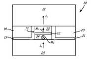
- FIG. 1is a front surface view of a tunneling magneto-resistive (TMR) reader including a free layer assembly having a perpendicular to the plane anisotropy and side shields;
- TMRtunneling magneto-resistive
- FIG. 2is a graph showing the resistance across the tunneling magneto-resistive (TMR) reader as a function of the magnetic state of the free layer element;
- TMRtunneling magneto-resistive
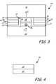
- FIG. 3is a front surface view of a tunneling magneto-resistive (TMR) reader including a free layer assembly having a perpendicular to the plane anisotropy and composite side shields;
- TMRtunneling magneto-resistive
- FIG. 4is a layer diagram of a composite free layer element
- FIG. 5is a cross-sectional schematic diagram of a sensor stack including a reference magnetic element having a synthetic antiferromagnet and antiferromagnetic layer and a free magnetic element having a perpendicular to the plane anisotropy;
- FIG. 6is a cross-sectional schematic diagram of a sensor stack including an extended reference magnetic element having a synthetic antiferromagnet and antiferromagnetic layer and a free magnetic element having a perpendicular to the plane anisotropy;
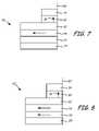
- FIG. 7is a cross-sectional schematic diagram of a sensor stack including an extended reference magnetic element having a pinned layer and antiferromagnetic layer and a free magnetic element having a perpendicular to the plane anisotropy; and
- FIG. 8is a cross-sectional schematic diagram of a sensor stack including an extended reference magnetic element having a pinned layer and a hard magnetic layer and a free magnetic element having a perpendicular to the plane anisotropy.
- topbottom
- bottomabove
- bottombelow
- Other layerssuch as seed or capping layers, are not depicted for clarity but could be included as technical need arises.
- the present disclosurerelates to a magnetic sensor with a perpendicular anisotropy free layer and side shields.
- the present disclosurecan improve the areal density capabilities of a tunneling magneto resistive (TMR) reader.
- TMRtunneling magneto resistive
- a number of sensor stack layer configurationsare described. These sensor stack configurations improve the reader's performance.
- Conventional permanent magnet side shieldsare eliminated with the designs described herein, thus eliminating some magnetic asymmetry or canting found in the conventional permanent magnet side shield designs. While the present disclosure is not so limited, an appreciation of various aspects of the disclosure will be gained through a discussion of the examples provided below.
- FIG. 1is a front surface view of a tunneling magneto-resistive (TMR) reader 10 including a free layer assembly 30 having a perpendicular to the plane anisotropy and side shields 18 , 20 .
- the tunneling magneto-resistive (TMR) reader 10includes a sensor stack 12 separating a top magnetic shield 14 from a bottom magnetic shield 24 .
- the sensor stack 12includes a reference magnetic element 34 having a reference magnetization orientation M R direction a free magnetic element 30 having a free magnetization orientation M F direction substantially perpendicular to the reference magnetization orientation M R direction, and a non-magnetic spacer 32 layer separating the reference magnetic element 34 from the free magnetic element 30 .
- a first side magnetic shield 18 and a second side magnetic shield 20are disposed between the top magnetic shield 14 and the bottom magnetic shield 24 .
- the sensor stack 12is between the first side magnetic shield 18 and the second side magnetic shield 20 , and the first side magnetic shield 18 and the second side magnetic shield 20 include an electrically insulating layer 19 , 21 electrically insulating the top magnetic shield 14 from a bottom magnetic shield 24 .
- free magnetic element 30is on the top of sensor stack 12 and reference magnetic element 34 is on the bottom of sensor stack 12 .
- sensor stack 12may alternatively include reference magnetic element 34 on the top of sensor stack 12 and free magnetic element 30 on the bottom of sensor stack 12 .
- Free magnetic element 30is a single or a composite or multiple layer structure having a magnetization M F that rotates in response to an external magnetic field. Free magnetic element 30 has a magnetization M F with an effective direction that is perpendicular to the plane of each layer of free magnetic element 30 in a quiescent state due to the perpendicular anisotropy of the layer or layers of free magnetic element 30 . While the direction of magnetization M F in a quiescent state is shown directed toward the top of sensor stack 12 , the layer or layers of free magnetic element 30 may alternatively provide an effective magnetization direction that is directed toward the bottom of sensor stack 12 in a quiescent state.
- free magnetic element 30When free magnetic element 30 has perpendicular-to-the-plane anisotropy, canting of the magnetization proximate the edges of the layer or layers of free magnetic element 30 is prevented. This reduces noise in sensor stack 12 , thereby improving the signal generated, and improves the stability of sensor stack 12 .
- Spacer layer 32is a nonmagnetic layer disposed between free magnetic element 30 and reference magnetic element 34 .
- spacer layer 32is a nonmagnetic, conductive material, such as Cu, Ag, Au, or Ru, making magnetic sensor 10 a giant magnetoresistive sensor.
- spacer layer 32is a non-magnetic, insulative or semi-conductive material, such as oxides formed of Mg, Al, Hf, or Ti, making magnetic sensor 10 a tunneling magnetoresistive sensor.
- Reference magnetic element 34has a fixed magnetization direction M R that is in-plane with the layer or layers of magnetic element 34 . Magnetization direction M F of free magnetic element 30 is perpendicular to fixed magnetization direction M R in a quiescent state.
- Reference magnetic element 34may be a single ferromagnetic layer having an anisotropically defined magnetization direction.
- Reference magnetic element 34may also include various combinations of layers to provide magnetization M R having a fixed direction, such as a ferromagnetic pinned layer with an antiferromagnetic pinning layer, a synthetic ferromagnetic pinned layer (i.e., two ferromagnetic layers coupled by a nonmagnetic metal, such as Ru), or a synthetic ferromagnetic pinned layer coupled to an antiferromagnetic pinning layer.
- Ferromagnetic layers of reference layer assembly 34may be made of a ferromagnetic alloy, such as CoFe, NiFe, or NiFeCo, and the antiferromagnetic layer may be made of PtMn, IrMn, NiMn, or FeMn.
- reference magnetic element 34is replaced by a second free layer assembly having perpendicular-to-the-plane anisotropy.
- sense current I Sis passed through sensor stack 12 via leads/shields 14 and 24 such that the sense current I S passes perpendicular to the plane of the layer or layers of sensor stack 12 .
- the resistance of sensor stack 12changes as a function of the angle between magnetizations M F and M R .
- the voltage across sensor stack 12is measured between leads/shields 14 and 24 by external circuitry (not shown) to detect changes in resistance of sensor stack 12 .
- the response of sensor stack 12 to external magnetic fields, and the corresponding changes in resistance across sensor stack 12is shown and described with regard to FIG. 2 .
- FIG. 2is a graph showing the resistance across the tunneling magneto-resistive (TMR) reader 12 as a function of the magnetization orientation M F of the free layer element 30 .
- Layer diagrams 12 a, 12 b, and 12 cillustrate the various magnetic states of sensor stack 12 as viewed from the front surface.
- Layer diagram 12 aillustrates the states of magnetization M F and magnetization M R in a quiescent state (i.e., no external magnetic field), in which magnetization M F is perpendicular to the plane of free layer element 30 . In this state, the readback voltage across sensor stack 12 is approximately zero.
- Layer diagram 12 billustrates the states of magnetization M F and magnetization M R when sensor stack 12 is in the presence of an external magnetic field having a first direction.
- the external magnetic fieldcauses magnetization M F to rotate such that magnetization M F is parallel with magnetization M R .
- the voltage drop across sensor stack 12is negative when sense current I S is applied, which is plotted below the zero resistance line in FIG. 2 .
- Layer diagram 12 cillustrates the states of magnetization M F and magnetization M R when sensor stack 12 is in the presence of an external magnetic field having a second direction opposite the first direction.
- the external magnetic fieldcauses magnetization M F to rotate such that magnetization M F is anti-parallel with magnetization M R .
- the voltage drop across sensor stack 12is positive when sense current I S is applied, which is plotted above the zero resistance line in FIG. 2 .
- FIG. 3is a front surface view of a tunneling magneto-resistive (TMR) reader 40 including a free layer assembly having a perpendicular to the plane anisotropy and composite side shields 18 , 20 .
- the tunneling magneto-resistive (TMR) reader 40includes a sensor stack 12 separating a top magnetic shield 14 from a bottom magnetic shield 24 .
- the sensor stack 12includes a reference magnetic element having a reference magnetization orientation M R direction a free magnetic element having a free magnetization orientation M F direction substantially perpendicular to the reference magnetization orientation M R direction, and a non-magnetic spacer layer separating the reference magnetic element from the free magnetic element. As described above.
- a first composite side magnetic shield 18 and a second composite side magnetic shield 20are disposed between the top magnetic shield 14 and the bottom magnetic shield 24 .
- the sensor stack 12is between the first composite side magnetic shield 18 and the second composite side magnetic shield 20 , and the first composite side magnetic shield 18 and the second composite side magnetic shield 20 include an electrically insulating layer 19 , 21 electrically insulating the top magnetic shield 14 from a bottom magnetic shield 24 .
- the composite side magnetic shieldsinclude two or more layers magnetic layers separated by non-magnetic spacer layers.
- the first composite side magnetic shield 18includes a first magnetic layer 31 and a second magnetic layer 33 separated by a non-magnetic spacer layer 34
- the second composite side magnetic shield 20includes a first magnetic layer 41 and a second magnetic layer 43 separated by a non-magnetic spacer layer 44 .
- the non-magnetic spacer layer 34 , 44is a nonmagnetic, conductive material, such as Cu, Ag, Au, or Ru.
- the non-magnetic spacer layer 34 , 44is a non-magnetic, insulative or semi-conductive material, such as oxides formed of Mg, Al, Hf, or Ti.
- Non-magnetic, insulative or semi-conductive the non-magnetic spacer layers 34 , 44assist the electrically insulating layer 19 , 21 in electrically isolating the top magnetic shield 14 from the bottom magnetic shield 24 .
- FIG. 4is a layer diagram of a composite free magnetic element 30 .
- the free magnetic elements 30 described hereincan be a composite free magnetic element 30 .
- the composite free magnetic element 30can include a first layer 35 of CoFeB material and a second layer 36 of TbCoFe material.
- TbCoFe materialThere are other materials in addition to the TbCoFe that can be utilized to provide perpendicular anisotropy.
- a listing of these materialsincludes FePt, CoPt, Co/Pt multilayers, Co/Pd multilayers, Co/Cu multilayers, Co/Au multilayers, Co/Ni multilayers, and MnAl, for example.
- the first layer 35is in contact with the spacer layer ( 32 in FIG.
- first layer 35 and second layer 36 materialsare believed to be responsible for the TMR effect.
- TbCoFe materialis believed to create the perpendicular anisotropy.
- a strong exchange coupling between the first layer 35 and second layer 36 materialsinsures that the first layer 35 magnetization in the composite free magnetic element 30 is perpendicular to the plane of the composite free magnetic element 30 .
- FIG. 5is a cross-sectional schematic diagram of a sensor stack 50 including a reference layer having a synthetic antiferromagnet SAF and antiferromagnetic layer 77 and a free magnetic element 30 having a perpendicular to the plane anisotropy.
- Top and bottom leads/shields 14 and 24 , free magnetic element 30 , spacer layer 32 , and reference magnetic element 74 , 75 , 76 , 77define front surface 80 .
- front surface 80is substantially planar.
- the front surface 80or air bearing surface (ABS) faces, for example, magnetic media that is sensed by the sensor stack 50 .
- the synthetic antiferromagnet SAFis stabilized by the antiferromagnetic layer 77 .
- the synthetic antiferromagnet SAFcan be, for example, two ferromagnetic layers 74 , 76 coupled by a nonmagnetic, electrically conductive spacer layer 75 , such as Ru.
- Ferromagnetic layers of synthetic antiferromagnet SAFcan be, for example, made of a ferromagnetic alloy, such as CoFe, NiFe, or NiFeCo, and the antiferromagnetic layer 77 may be made of PtMn, IrMn, NiMn, or FeMn.
- FIG. 6is a cross-sectional schematic diagram of a sensor stack 51 including an extended magnetic reference element 74 , 75 , 76 , 77 , having a synthetic antiferromagnet SAF and antiferromagnetic layer 77 and a free magnetic element 30 having a perpendicular to the plane anisotropy.
- Top and bottom leads/shields 14 and 24 , free magnetic element 30 , spacer layer 32 , and reference magnetic element 74 , 75 , 76 , 77define front surface 80 .
- front surface 80is substantially planar.
- the front surface 80or air bearing surface (ABS) faces, for example, magnetic media that is sensed by the sensor stack 51 .
- the synthetic antiferromagnet SAFis stabilized by the antiferromagnetic layer 77 .
- the synthetic antiferromagnet SAFcan be, for example, two ferromagnetic layers 74 , 76 coupled by a nonmagnetic, electrically conductive spacer layer 75 , such as Ru.
- Ferromagnetic layers of synthetic antiferromagnet SAFcan be, for example, made of a ferromagnetic alloy, such as CoFe, NiFe, or NiFeCo, and the antiferromagnetic layer 77 may be made of PtMn, IrMn, NiMn, or FeMn.
- the magnetic reference element 74 , 75 , 76 , 77extends a larger distance away from the front surface than the free magnetic element 30 having a perpendicular to the plane anisotropy.
- the free magnetic element 30has a length that is less than the length of the magnetic reference element 74 , 75 , 76 , 77 . This improves the magnetic stability of the synthetic antiferromagnet SAF.
- FIG. 7is a cross-sectional schematic diagram of a sensor stack 52 including an extended reference magnetic element having a pinned layer 74 and antiferromagnetic layer 77 and a free magnetic element 30 having a perpendicular to the plane anisotropy.
- Top and bottom leads/shields 14 and 24 , free magnetic element 30 , spacer layer 32 , and reference magnetic element 74 , 77define front surface 80 .
- front surface 80is substantially planar.
- the front surface 80or air bearing surface (ABS) faces, for example, magnetic media that is sensed by the sensor stack 52 .
- the magnetic reference elementincludes a single pinned layer 74 that has a length that is greater than the length of the free magnetic element 30 .
- the single pinned layer 74is stabilized by an antiferromagnetic layer 77 .
- the extended single pinned layer 74the in-plane magnetic field from the pinned layer acting on the free magnetic element 30 will be small and will not change its angle substantially from the perpendicular direction.
- FIG. 8is a cross-sectional schematic diagram of a sensor stack 53 including an extended reference magnetic element having a pinned layer 74 and a hard magnetic layer 79 and a free magnetic element 30 having a perpendicular to the plane anisotropy.
- Top and bottom leads/shields 14 and 24 , free magnetic element 30 , spacer layer 32 , and reference magnetic element 74 , 79define front surface 80 .
- front surface 80is substantially planar.
- the front surface 80or air bearing surface (ABS) faces, for example, magnetic media that is sensed by the sensor stack 53 .
- the magnetic reference elementincludes a single pinned layer 74 that has a length that is greater than the length of the free magnetic element 30 .
- the single pinned layer 74is stabilized by a hard magnetic layer 79 .
- the extended single pinned layer 74the in-plane magnetic field from the pinned layer acting on the free magnetic element 30 will be small and will not change its angle substantially from the perpendicular direction.
- the extended single pinned layer 74can be formed of ferromagnetic material such as, CoFeB for a large TMR, wile the hard magnetic layer can be formed of materials with a large in-place Hk and Hc like, CoPt, CoCrPt, and/or FePt.
Landscapes
- Engineering & Computer Science (AREA)
- Manufacturing & Machinery (AREA)
- Physics & Mathematics (AREA)
- Condensed Matter Physics & Semiconductors (AREA)
- General Physics & Mathematics (AREA)
- Hall/Mr Elements (AREA)
- Magnetic Heads (AREA)
Abstract
Description
Claims (20)
Priority Applications (5)
| Application Number | Priority Date | Filing Date | Title |
|---|---|---|---|
| US12/502,204US8125746B2 (en) | 2009-07-13 | 2009-07-13 | Magnetic sensor with perpendicular anisotrophy free layer and side shields |
| JP2010136170AJP2011023096A (en) | 2009-07-13 | 2010-06-15 | Tunnel magnetoresistance reproduction element |
| MYPI2010002974MY152697A (en) | 2009-07-13 | 2010-06-22 | Magnetic sensor with perpendicular anisotrophy free layer and side shields |
| CN2010102270670ACN101958123A (en) | 2009-07-13 | 2010-06-29 | Magnetic Sensor with perpendicular magnetic anisotropy free layer and side direction shield member |
| US13/354,838US8482883B2 (en) | 2009-07-13 | 2012-01-20 | Magnetic sensor with perpendicular anisotrophy free layer and side shields |
Applications Claiming Priority (1)
| Application Number | Priority Date | Filing Date | Title |
|---|---|---|---|
| US12/502,204US8125746B2 (en) | 2009-07-13 | 2009-07-13 | Magnetic sensor with perpendicular anisotrophy free layer and side shields |
Related Child Applications (1)
| Application Number | Title | Priority Date | Filing Date |
|---|---|---|---|
| US13/354,838ContinuationUS8482883B2 (en) | 2009-07-13 | 2012-01-20 | Magnetic sensor with perpendicular anisotrophy free layer and side shields |
Publications (2)
| Publication Number | Publication Date |
|---|---|
| US20110007429A1 US20110007429A1 (en) | 2011-01-13 |
| US8125746B2true US8125746B2 (en) | 2012-02-28 |
Family
ID=43427291
Family Applications (2)
| Application Number | Title | Priority Date | Filing Date |
|---|---|---|---|
| US12/502,204Expired - Fee RelatedUS8125746B2 (en) | 2009-07-13 | 2009-07-13 | Magnetic sensor with perpendicular anisotrophy free layer and side shields |
| US13/354,838ActiveUS8482883B2 (en) | 2009-07-13 | 2012-01-20 | Magnetic sensor with perpendicular anisotrophy free layer and side shields |
Family Applications After (1)
| Application Number | Title | Priority Date | Filing Date |
|---|---|---|---|
| US13/354,838ActiveUS8482883B2 (en) | 2009-07-13 | 2012-01-20 | Magnetic sensor with perpendicular anisotrophy free layer and side shields |
Country Status (4)
| Country | Link |
|---|---|
| US (2) | US8125746B2 (en) |
| JP (1) | JP2011023096A (en) |
| CN (1) | CN101958123A (en) |
| MY (1) | MY152697A (en) |
Cited By (21)
| Publication number | Priority date | Publication date | Assignee | Title |
|---|---|---|---|---|
| US8576518B1 (en) | 2012-10-30 | 2013-11-05 | HGST Netherlands B.V. | Current-perpendicular-to-the-plane (CPP) magnetoresistive (MR) sensor with exchange-coupled side shield structure |
| US8773821B2 (en)* | 2012-10-05 | 2014-07-08 | Nve Corporation | Magnetoresistive-based mixed anisotropy high field sensor |
| US8780506B1 (en) | 2013-06-20 | 2014-07-15 | HGST Netherlands B.V. | Current-perpendicular-to-the-plane (CPP) magnetoresistive (MR) sensor with side shields and an antiparallel structure top shield |
| US8885300B2 (en) | 2013-02-07 | 2014-11-11 | Seagate Technology Llc | Magnetic element with a bi-layer side shield |
| US8922951B2 (en)* | 2012-12-11 | 2014-12-30 | Seagate Technology Llc | Data storage device with variable anisotropy side shield |
| US8995096B2 (en) | 2013-03-16 | 2015-03-31 | Seagate Technology Llc | Magnetic element side shield with diffusion barrier |
| US9042060B2 (en) | 2013-09-25 | 2015-05-26 | HGST Netherlands B.V. | Magnetic head having a long throat height pinned layer with a short height hard bias layer |
| US9251816B2 (en) | 2013-10-03 | 2016-02-02 | Seagate Technology Llc | Magnetic sensor shield pinned by a high-coercivity ferromagnet |
| US20180247667A1 (en)* | 2016-02-03 | 2018-08-30 | International Business Machines Corporation | Tunnel magnetoresistive sensor having conductive ceramic layers |
| US11100946B1 (en) | 2020-07-01 | 2021-08-24 | Western Digital Technologies, Inc. | SOT differential reader and method of making same |
| US11489108B2 (en) | 2020-04-28 | 2022-11-01 | Western Digital Technologies, Inc. | BiSb topological insulator with seed layer or interlayer to prevent sb diffusion and promote BiSb (012) orientation |
| US11495741B2 (en) | 2020-06-30 | 2022-11-08 | Western Digital Technologies, Inc. | Bismuth antimony alloys for use as topological insulators |
| US11532323B1 (en) | 2021-08-18 | 2022-12-20 | Western Digital Technologies, Inc. | BiSbX (012) layers having increased operating temperatures for SOT and MRAM devices |
| US11763973B2 (en) | 2021-08-13 | 2023-09-19 | Western Digital Technologies, Inc. | Buffer layers and interlayers that promote BiSbx (012) alloy orientation for SOT and MRAM devices |
| US11776567B2 (en) | 2020-07-09 | 2023-10-03 | Western Digital Technologies, Inc. | SOT film stack for differential reader |
| US11783853B1 (en) | 2022-05-31 | 2023-10-10 | Western Digital Technologies, Inc. | Topological insulator based spin torque oscillator reader |
| US11875827B2 (en) | 2022-03-25 | 2024-01-16 | Western Digital Technologies, Inc. | SOT reader using BiSb topological insulator |
| US11875828B2 (en) | 2021-10-14 | 2024-01-16 | Seagate Technology Llc | Magnetic storage reader having a bridge to align magnetic moments |
| US12125512B2 (en) | 2021-12-22 | 2024-10-22 | Western Digital Technologies, Inc. | Doping process to refine grain size for smoother BiSb film surface |
| US12154603B1 (en) | 2023-06-14 | 2024-11-26 | Western Digital Technologies, Inc. | Spin-orbit torque (SOT) writer with topological insulator materials |
| US12354627B2 (en) | 2023-06-28 | 2025-07-08 | Western Digital Technologies, Inc. | Higher areal density non-local spin orbit torque (SOT) writer with topological insulator materials |
Families Citing this family (40)
| Publication number | Priority date | Publication date | Assignee | Title |
|---|---|---|---|---|
| US8953285B2 (en)* | 2010-05-05 | 2015-02-10 | Headway Technologies, Inc. | Side shielded magnetoresistive (MR) read head with perpendicular magnetic free layer |
| US8089734B2 (en)* | 2010-05-17 | 2012-01-03 | Tdk Corporation | Magnetoresistive element having a pair of side shields |
| US8922956B2 (en) | 2010-06-04 | 2014-12-30 | Seagate Technology Llc | Tunneling magneto-resistive sensors with buffer layers |
| JP5736836B2 (en)* | 2011-02-23 | 2015-06-17 | Tdk株式会社 | Spin conduction type magnetic sensor |
| US8467154B2 (en)* | 2011-08-31 | 2013-06-18 | Seagate Technology Llc | Magnetic sensors having perpendicular anisotropy free layer |
| US9007818B2 (en)* | 2012-03-22 | 2015-04-14 | Micron Technology, Inc. | Memory cells, semiconductor device structures, systems including such cells, and methods of fabrication |
| US9054030B2 (en) | 2012-06-19 | 2015-06-09 | Micron Technology, Inc. | Memory cells, semiconductor device structures, memory systems, and methods of fabrication |
| US8923038B2 (en) | 2012-06-19 | 2014-12-30 | Micron Technology, Inc. | Memory cells, semiconductor device structures, memory systems, and methods of fabrication |
| US8780508B2 (en)* | 2012-06-29 | 2014-07-15 | Seagate Technology Llc | Magnetic element with biased side shield lamination |
| US20140177102A1 (en) | 2012-12-21 | 2014-06-26 | Seagate Technology Llc | Multi-reader method and apparatus |
| US9379315B2 (en) | 2013-03-12 | 2016-06-28 | Micron Technology, Inc. | Memory cells, methods of fabrication, semiconductor device structures, and memory systems |
| US20140268417A1 (en)* | 2013-03-16 | 2014-09-18 | Seagate Technology Llc | Bottom shield stabilized magnetic seed layer |
| US20140355152A1 (en)* | 2013-05-29 | 2014-12-04 | HGST Netherlands B.V. | Interlayer coupled free layer with out of plane magnetic orientation for magnetic read head |
| US9368714B2 (en) | 2013-07-01 | 2016-06-14 | Micron Technology, Inc. | Memory cells, methods of operation and fabrication, semiconductor device structures, and memory systems |
| US9466787B2 (en) | 2013-07-23 | 2016-10-11 | Micron Technology, Inc. | Memory cells, methods of fabrication, semiconductor device structures, memory systems, and electronic systems |
| US9461242B2 (en) | 2013-09-13 | 2016-10-04 | Micron Technology, Inc. | Magnetic memory cells, methods of fabrication, semiconductor devices, memory systems, and electronic systems |
| US9608197B2 (en) | 2013-09-18 | 2017-03-28 | Micron Technology, Inc. | Memory cells, methods of fabrication, and semiconductor devices |
| US9472214B1 (en) | 2013-10-14 | 2016-10-18 | Seagate Technology Llc | Reader side shield |
| US9214172B2 (en)* | 2013-10-23 | 2015-12-15 | Western Digital (Fremont), Llc | Method of manufacturing a magnetic read head |
| US9087535B2 (en) | 2013-10-31 | 2015-07-21 | Seagate Technology Llc | Spin transport sensor |
| US8953284B1 (en)* | 2013-11-20 | 2015-02-10 | HGST Netherlands B.V. | Multi-read sensor having a narrow read gap structure |
| US9230575B2 (en)* | 2013-12-13 | 2016-01-05 | Seagate Technology Llc | Magnetoresistive sensor with SAF structure having crystalline layer and amorphous layer |
| US9053720B1 (en)* | 2014-01-10 | 2015-06-09 | Headway Technologies, Inc. | High moment wrap shields for magnetic read head to improve micro-magnetic read width |
| US20150213815A1 (en)* | 2014-01-29 | 2015-07-30 | Seagate Technology Llc | Synthetic antiferromagnetic reader |
| US10454024B2 (en) | 2014-02-28 | 2019-10-22 | Micron Technology, Inc. | Memory cells, methods of fabrication, and memory devices |
| US9396743B1 (en)* | 2014-02-28 | 2016-07-19 | Western Digital (Fremont), Llc | Systems and methods for controlling soft bias thickness for tunnel magnetoresistance readers |
| US9281466B2 (en) | 2014-04-09 | 2016-03-08 | Micron Technology, Inc. | Memory cells, semiconductor structures, semiconductor devices, and methods of fabrication |
| US9269888B2 (en) | 2014-04-18 | 2016-02-23 | Micron Technology, Inc. | Memory cells, methods of fabrication, and semiconductor devices |
| WO2016012467A1 (en)* | 2014-07-22 | 2016-01-28 | Koninklijke Philips N.V. | Flexible coiled artery wick |
| US9349945B2 (en) | 2014-10-16 | 2016-05-24 | Micron Technology, Inc. | Memory cells, semiconductor devices, and methods of fabrication |
| US9768377B2 (en) | 2014-12-02 | 2017-09-19 | Micron Technology, Inc. | Magnetic cell structures, and methods of fabrication |
| US10439131B2 (en) | 2015-01-15 | 2019-10-08 | Micron Technology, Inc. | Methods of forming semiconductor devices including tunnel barrier materials |
| JP6928307B2 (en)* | 2017-03-28 | 2021-09-01 | 愛知製鋼株式会社 | Marker detection system and marker detection method |
| US10261138B2 (en)* | 2017-07-12 | 2019-04-16 | Nxp B.V. | Magnetic field sensor with magnetic field shield structure and systems incorporating same |
| US10852369B2 (en)* | 2019-01-09 | 2020-12-01 | Infineon Technologies Ag | Stray field robust xMR sensor using perpendicular anisotropy |
| US11385306B2 (en)* | 2019-08-23 | 2022-07-12 | Western Digital Technologies, Inc. | TMR sensor with magnetic tunnel junctions with shape anisotropy |
| DE102019126320B4 (en)* | 2019-09-30 | 2024-03-28 | Infineon Technologies Ag | Magnetoresistive sensor and manufacturing process for a magnetoresistive sensor |
| US11758819B2 (en) | 2020-12-15 | 2023-09-12 | International Business Machines Corporation | Magneto-resistive random access memory with laterally-recessed free layer |
| CN114664330B (en)* | 2020-12-23 | 2024-10-29 | 西部数据技术公司 | Dual free layer reader head with magnetic seed layer decoupled from shield |
| CN113889151B (en)* | 2021-10-21 | 2023-05-26 | 郑州云海信息技术有限公司 | Mechanical hard disk data reading and writing method and system based on ferromagnetic material |
Citations (12)
| Publication number | Priority date | Publication date | Assignee | Title |
|---|---|---|---|---|
| US6713800B2 (en) | 2002-06-27 | 2004-03-30 | Seagate Technology Llc | Magnetoresistive sensor with reduced side-reading effect |
| US6943993B2 (en) | 2003-02-11 | 2005-09-13 | Western Digital (Fremont), Inc. | Magnetic recording head with a side shield structure for controlling side reading of thin film read sensor |
| US6967863B2 (en) | 2004-02-25 | 2005-11-22 | Grandis, Inc. | Perpendicular magnetization magnetic element utilizing spin transfer |
| US6992359B2 (en) | 2004-02-26 | 2006-01-31 | Grandis, Inc. | Spin transfer magnetic element with free layers having high perpendicular anisotropy and in-plane equilibrium magnetization |
| US7102854B2 (en) | 2003-10-03 | 2006-09-05 | Seagate Technology Llc | Transducing head with reduced side writing |
| US20070026538A1 (en)* | 2005-07-29 | 2007-02-01 | Hitachi Global Storage Technologies Netherlands B.V. | Deposition defined trackwidth for very narrow trackwidth CPP device |
| US20070081279A1 (en)* | 2005-10-06 | 2007-04-12 | Hitachi Global Storage Technologies | Double mill process for patterning current perpendicular to plane (CPP) magnetoresistive devices to minimize barrier shorting and barrier damage |
| US20090257153A1 (en)* | 2008-04-10 | 2009-10-15 | Headway Technologies, Inc. | Binary output reader structure (BORS) with high utilization rate |
| US20100097722A1 (en)* | 2008-10-21 | 2010-04-22 | Tdk Corporation | Magnetoresistive device of the cpp type, and magnetic disk system |
| US20100214701A1 (en)* | 2009-02-26 | 2010-08-26 | Tdk Corporation | Magnetoresistive effect element in cpp-type structure and magnetic disk device |
| US20100232072A1 (en)* | 2009-03-16 | 2010-09-16 | Seagate Technology Llc | Magnetic sensor with a recessed reference layer assembly and a front shield |
| US20110014390A1 (en)* | 2006-11-16 | 2011-01-20 | Headway Technologies, Inc. | Enhanced hard bias in thin film magnetoresistive sensors with perpendicular easy axis growth of hard bias and strong shield-hard bias coupling |
Family Cites Families (11)
| Publication number | Priority date | Publication date | Assignee | Title |
|---|---|---|---|---|
| JP2002025014A (en)* | 2000-07-06 | 2002-01-25 | Sony Corp | Magnetic tunnel effect type magnetic head and recording and reproducing device |
| JP2004103120A (en)* | 2002-09-10 | 2004-04-02 | Hitachi Ltd | Separate read / write magnetic head with differential bias type magnetic domain control structure |
| JP2004152334A (en)* | 2002-10-29 | 2004-05-27 | Hitachi Ltd | Magnetic sensor, method of manufacturing the same, and magnetic recording / reproducing apparatus equipped with the same |
| JP2004259330A (en)* | 2003-02-25 | 2004-09-16 | Hitachi Ltd | Magnetic head |
| US7602591B2 (en) | 2005-06-22 | 2009-10-13 | Tdk Corporation | Exchange-coupled free layer with out-of-plane magnetization |
| KR100763904B1 (en)* | 2005-08-12 | 2007-10-05 | 삼성전자주식회사 | Vertical magnetic head and its manufacturing method |
| US7969684B2 (en)* | 2006-03-28 | 2011-06-28 | Hitachi Global Storage Technologies Netherlands B.V. | Write head design and method for reducing adjacent track interference at very narrow track widths |
| JP5113163B2 (en) | 2007-05-11 | 2013-01-09 | アルプス電気株式会社 | Tunnel type magnetic sensor |
| JP2008288235A (en)* | 2007-05-15 | 2008-11-27 | Tdk Corp | Magnetic detecting element and manufacturing method thereof |
| US9007727B2 (en)* | 2007-07-17 | 2015-04-14 | HGST Netherlands B.V. | Magnetic head having CPP sensor with improved stabilization of the magnetization of the pinned magnetic layer |
| US7869165B2 (en) | 2007-07-30 | 2011-01-11 | Tdk Corporation | Magnetic field detecting element having stack with a plurality of free layers and side shield layers |
- 2009
- 2009-07-13USUS12/502,204patent/US8125746B2/ennot_activeExpired - Fee Related
- 2010
- 2010-06-15JPJP2010136170Apatent/JP2011023096A/enactivePending
- 2010-06-22MYMYPI2010002974patent/MY152697A/enunknown
- 2010-06-29CNCN2010102270670Apatent/CN101958123A/enactivePending
- 2012
- 2012-01-20USUS13/354,838patent/US8482883B2/enactiveActive
Patent Citations (12)
| Publication number | Priority date | Publication date | Assignee | Title |
|---|---|---|---|---|
| US6713800B2 (en) | 2002-06-27 | 2004-03-30 | Seagate Technology Llc | Magnetoresistive sensor with reduced side-reading effect |
| US6943993B2 (en) | 2003-02-11 | 2005-09-13 | Western Digital (Fremont), Inc. | Magnetic recording head with a side shield structure for controlling side reading of thin film read sensor |
| US7102854B2 (en) | 2003-10-03 | 2006-09-05 | Seagate Technology Llc | Transducing head with reduced side writing |
| US6967863B2 (en) | 2004-02-25 | 2005-11-22 | Grandis, Inc. | Perpendicular magnetization magnetic element utilizing spin transfer |
| US6992359B2 (en) | 2004-02-26 | 2006-01-31 | Grandis, Inc. | Spin transfer magnetic element with free layers having high perpendicular anisotropy and in-plane equilibrium magnetization |
| US20070026538A1 (en)* | 2005-07-29 | 2007-02-01 | Hitachi Global Storage Technologies Netherlands B.V. | Deposition defined trackwidth for very narrow trackwidth CPP device |
| US20070081279A1 (en)* | 2005-10-06 | 2007-04-12 | Hitachi Global Storage Technologies | Double mill process for patterning current perpendicular to plane (CPP) magnetoresistive devices to minimize barrier shorting and barrier damage |
| US20110014390A1 (en)* | 2006-11-16 | 2011-01-20 | Headway Technologies, Inc. | Enhanced hard bias in thin film magnetoresistive sensors with perpendicular easy axis growth of hard bias and strong shield-hard bias coupling |
| US20090257153A1 (en)* | 2008-04-10 | 2009-10-15 | Headway Technologies, Inc. | Binary output reader structure (BORS) with high utilization rate |
| US20100097722A1 (en)* | 2008-10-21 | 2010-04-22 | Tdk Corporation | Magnetoresistive device of the cpp type, and magnetic disk system |
| US20100214701A1 (en)* | 2009-02-26 | 2010-08-26 | Tdk Corporation | Magnetoresistive effect element in cpp-type structure and magnetic disk device |
| US20100232072A1 (en)* | 2009-03-16 | 2010-09-16 | Seagate Technology Llc | Magnetic sensor with a recessed reference layer assembly and a front shield |
Non-Patent Citations (1)
| Title |
|---|
| U.S. Appl. No. 12/017,822, filed Jan. 22, 2008, Dimitrov. |
Cited By (27)
| Publication number | Priority date | Publication date | Assignee | Title |
|---|---|---|---|---|
| US8773821B2 (en)* | 2012-10-05 | 2014-07-08 | Nve Corporation | Magnetoresistive-based mixed anisotropy high field sensor |
| US8576518B1 (en) | 2012-10-30 | 2013-11-05 | HGST Netherlands B.V. | Current-perpendicular-to-the-plane (CPP) magnetoresistive (MR) sensor with exchange-coupled side shield structure |
| US8922951B2 (en)* | 2012-12-11 | 2014-12-30 | Seagate Technology Llc | Data storage device with variable anisotropy side shield |
| US8885300B2 (en) | 2013-02-07 | 2014-11-11 | Seagate Technology Llc | Magnetic element with a bi-layer side shield |
| US8995096B2 (en) | 2013-03-16 | 2015-03-31 | Seagate Technology Llc | Magnetic element side shield with diffusion barrier |
| US8780506B1 (en) | 2013-06-20 | 2014-07-15 | HGST Netherlands B.V. | Current-perpendicular-to-the-plane (CPP) magnetoresistive (MR) sensor with side shields and an antiparallel structure top shield |
| US9042060B2 (en) | 2013-09-25 | 2015-05-26 | HGST Netherlands B.V. | Magnetic head having a long throat height pinned layer with a short height hard bias layer |
| US9251816B2 (en) | 2013-10-03 | 2016-02-02 | Seagate Technology Llc | Magnetic sensor shield pinned by a high-coercivity ferromagnet |
| US20180247667A1 (en)* | 2016-02-03 | 2018-08-30 | International Business Machines Corporation | Tunnel magnetoresistive sensor having conductive ceramic layers |
| US10586561B2 (en)* | 2016-02-03 | 2020-03-10 | International Business Machines Corporation | Tunnel magnetoresistive sensor having conductive ceramic layers |
| US11037587B2 (en) | 2016-02-03 | 2021-06-15 | International Business Machines Corporation | Tunnel magnetoresistive sensor having conductive ceramic layers |
| US11489108B2 (en) | 2020-04-28 | 2022-11-01 | Western Digital Technologies, Inc. | BiSb topological insulator with seed layer or interlayer to prevent sb diffusion and promote BiSb (012) orientation |
| US11495741B2 (en) | 2020-06-30 | 2022-11-08 | Western Digital Technologies, Inc. | Bismuth antimony alloys for use as topological insulators |
| US11100946B1 (en) | 2020-07-01 | 2021-08-24 | Western Digital Technologies, Inc. | SOT differential reader and method of making same |
| US11615809B2 (en) | 2020-07-01 | 2023-03-28 | Western Digital Technologies, Inc. | SOT differential reader and method of making same |
| US11776567B2 (en) | 2020-07-09 | 2023-10-03 | Western Digital Technologies, Inc. | SOT film stack for differential reader |
| US12408560B2 (en) | 2021-08-13 | 2025-09-02 | Western Digital Technologies, Inc. | Buffer layers and interlayers that promote BiSbx (012) alloy orientation for sot and MRAM devices |
| US11763973B2 (en) | 2021-08-13 | 2023-09-19 | Western Digital Technologies, Inc. | Buffer layers and interlayers that promote BiSbx (012) alloy orientation for SOT and MRAM devices |
| US11908496B2 (en) | 2021-08-18 | 2024-02-20 | Western Digital Technologies, Inc. | BiSbX (012) layers having increased operating temperatures for SOT and MRAM devices |
| US11532323B1 (en) | 2021-08-18 | 2022-12-20 | Western Digital Technologies, Inc. | BiSbX (012) layers having increased operating temperatures for SOT and MRAM devices |
| US11875828B2 (en) | 2021-10-14 | 2024-01-16 | Seagate Technology Llc | Magnetic storage reader having a bridge to align magnetic moments |
| US12125512B2 (en) | 2021-12-22 | 2024-10-22 | Western Digital Technologies, Inc. | Doping process to refine grain size for smoother BiSb film surface |
| US11875827B2 (en) | 2022-03-25 | 2024-01-16 | Western Digital Technologies, Inc. | SOT reader using BiSb topological insulator |
| US11783853B1 (en) | 2022-05-31 | 2023-10-10 | Western Digital Technologies, Inc. | Topological insulator based spin torque oscillator reader |
| US12125508B2 (en) | 2022-05-31 | 2024-10-22 | Western Digital Technologies, Inc. | Topological insulator based spin torque oscillator reader |
| US12154603B1 (en) | 2023-06-14 | 2024-11-26 | Western Digital Technologies, Inc. | Spin-orbit torque (SOT) writer with topological insulator materials |
| US12354627B2 (en) | 2023-06-28 | 2025-07-08 | Western Digital Technologies, Inc. | Higher areal density non-local spin orbit torque (SOT) writer with topological insulator materials |
Also Published As
| Publication number | Publication date |
|---|---|
| MY152697A (en) | 2014-11-28 |
| US20110007429A1 (en) | 2011-01-13 |
| CN101958123A (en) | 2011-01-26 |
| US8482883B2 (en) | 2013-07-09 |
| JP2011023096A (en) | 2011-02-03 |
| US20130021697A1 (en) | 2013-01-24 |
Similar Documents
| Publication | Publication Date | Title |
|---|---|---|
| US8125746B2 (en) | Magnetic sensor with perpendicular anisotrophy free layer and side shields | |
| US7929258B2 (en) | Magnetic sensor including a free layer having perpendicular to the plane anisotropy | |
| US8395867B2 (en) | Magnetic sensor with a recessed reference layer assembly and a front shield | |
| US9001472B2 (en) | Shield stabilization configuration with applied bias | |
| US8437105B2 (en) | Magnetic sensor with composite magnetic shield | |
| US9633679B2 (en) | Sensor stack structure with RKKY coupling layer between free layer and capping layer | |
| US8514525B2 (en) | Current-perpendicular-to-the-plane (CPP) magnetoresistive (MR) sensor with reference layer integrated in magnetic shield | |
| KR101566291B1 (en) | Magnetic element with coupled side shield | |
| US20110007426A1 (en) | Trapezoidal back bias and trilayer reader geometry to enhance device performance | |
| US20110228428A1 (en) | Trilayer reader with current constraint at the abs | |
| US8929034B2 (en) | Devices and methods using recessed electron spin analyzers | |
| US20110134572A1 (en) | Double biasing for trilayer mr sensors | |
| US20060114620A1 (en) | Granular type free layer and magnetic head | |
| US7872837B2 (en) | Method and apparatus for providing a magnetic read sensor having a thin pinning layer and improved magnetoreistive coefficient | |
| US8520344B2 (en) | Magnetoresistive device with enhanced pinned layer | |
| US20120161263A1 (en) | Current perpendicular to plane (CPP) magnetoresistive sensor having dual composition hard bias layer | |
| WO2008020817A1 (en) | Read head and magnetic device comprising the same | |
| US9087525B2 (en) | Layered synthetic anti-ferromagnetic upper shield | |
| US7583482B2 (en) | Magnetoresistive element and magnetoresistive device having a free layer stabilized by an in-stack bias | |
| US20080007877A1 (en) | Magneto-resistance effect element, magnetic head, magnetic recording/reproducing device and magnetic memory | |
| US9454979B1 (en) | Sensor structure with multilayer top shield | |
| US9099120B1 (en) | Interlayer coupling field control in tunneling magnetoresistive read heads |
Legal Events
| Date | Code | Title | Description |
|---|---|---|---|
| AS | Assignment | Owner name:SEAGATE TECHNOLOGY LLC, CALIFORNIA Free format text:ASSIGNMENT OF ASSIGNORS INTEREST;ASSIGNORS:DIMITROV, DIMITAR V.;GAO, ZHENG;JUNG, WONJOON;AND OTHERS;SIGNING DATES FROM 20090709 TO 20090805;REEL/FRAME:023066/0554 | |
| AS | Assignment | Owner name:THE BANK OF NOVA SCOTIA, AS ADMINISTRATIVE AGENT, CANADA Free format text:SECURITY AGREEMENT;ASSIGNOR:SEAGATE TECHNOLOGY LLC;REEL/FRAME:026010/0350 Effective date:20110118 Owner name:THE BANK OF NOVA SCOTIA, AS ADMINISTRATIVE AGENT, Free format text:SECURITY AGREEMENT;ASSIGNOR:SEAGATE TECHNOLOGY LLC;REEL/FRAME:026010/0350 Effective date:20110118 | |
| ZAAA | Notice of allowance and fees due | Free format text:ORIGINAL CODE: NOA | |
| ZAAB | Notice of allowance mailed | Free format text:ORIGINAL CODE: MN/=. | |
| STCF | Information on status: patent grant | Free format text:PATENTED CASE | |
| AS | Assignment | Owner name:THE BANK OF NOVA SCOTIA, AS ADMINISTRATIVE AGENT, CANADA Free format text:SECURITY AGREEMENT;ASSIGNORS:SEAGATE TECHNOLOGY LLC;EVAULT, INC. (F/K/A I365 INC.);SEAGATE TECHNOLOGY US HOLDINGS, INC.;REEL/FRAME:029127/0527 Effective date:20120718 Owner name:WELLS FARGO BANK, NATIONAL ASSOCIATION, AS COLLATERAL AGENT, CALIFORNIA Free format text:SECOND LIEN PATENT SECURITY AGREEMENT;ASSIGNORS:SEAGATE TECHNOLOGY LLC;EVAULT, INC. (F/K/A I365 INC.);SEAGATE TECHNOLOGY US HOLDINGS, INC.;REEL/FRAME:029253/0585 Effective date:20120718 Owner name:THE BANK OF NOVA SCOTIA, AS ADMINISTRATIVE AGENT, Free format text:SECURITY AGREEMENT;ASSIGNORS:SEAGATE TECHNOLOGY LLC;EVAULT, INC. (F/K/A I365 INC.);SEAGATE TECHNOLOGY US HOLDINGS, INC.;REEL/FRAME:029127/0527 Effective date:20120718 Owner name:WELLS FARGO BANK, NATIONAL ASSOCIATION, AS COLLATE Free format text:SECOND LIEN PATENT SECURITY AGREEMENT;ASSIGNORS:SEAGATE TECHNOLOGY LLC;EVAULT, INC. (F/K/A I365 INC.);SEAGATE TECHNOLOGY US HOLDINGS, INC.;REEL/FRAME:029253/0585 Effective date:20120718 | |
| CC | Certificate of correction | ||
| FPAY | Fee payment | Year of fee payment:4 | |
| MAFP | Maintenance fee payment | Free format text:PAYMENT OF MAINTENANCE FEE, 8TH YEAR, LARGE ENTITY (ORIGINAL EVENT CODE: M1552); ENTITY STATUS OF PATENT OWNER: LARGE ENTITY Year of fee payment:8 | |
| FEPP | Fee payment procedure | Free format text:MAINTENANCE FEE REMINDER MAILED (ORIGINAL EVENT CODE: REM.); ENTITY STATUS OF PATENT OWNER: LARGE ENTITY | |
| LAPS | Lapse for failure to pay maintenance fees | Free format text:PATENT EXPIRED FOR FAILURE TO PAY MAINTENANCE FEES (ORIGINAL EVENT CODE: EXP.); ENTITY STATUS OF PATENT OWNER: LARGE ENTITY | |
| STCH | Information on status: patent discontinuation | Free format text:PATENT EXPIRED DUE TO NONPAYMENT OF MAINTENANCE FEES UNDER 37 CFR 1.362 | |
| FP | Lapsed due to failure to pay maintenance fee | Effective date:20240228 | |
| AS | Assignment | Owner name:SEAGATE TECHNOLOGY US HOLDINGS, INC., CALIFORNIA Free format text:RELEASE BY SECURED PARTY;ASSIGNOR:WELLS FARGO BANK, NATIONAL ASSOCIATION, AS COLLATERAL AGENT;REEL/FRAME:067471/0955 Effective date:20240516 Owner name:EVAULT, INC. (F/K/A I365 INC.), CALIFORNIA Free format text:RELEASE BY SECURED PARTY;ASSIGNOR:WELLS FARGO BANK, NATIONAL ASSOCIATION, AS COLLATERAL AGENT;REEL/FRAME:067471/0955 Effective date:20240516 Owner name:SEAGATE TECHNOLOGY LLC, CALIFORNIA Free format text:RELEASE BY SECURED PARTY;ASSIGNOR:WELLS FARGO BANK, NATIONAL ASSOCIATION, AS COLLATERAL AGENT;REEL/FRAME:067471/0955 Effective date:20240516 | |
| AS | Assignment | Owner name:EVAULT INC, CALIFORNIA Free format text:RELEASE BY SECURED PARTY;ASSIGNOR:WELLS FARGO BANK, NATIONAL ASSOCIATION, AS COLLATERAL AGENT;REEL/FRAME:068457/0076 Effective date:20240723 Owner name:SEAGATE TECHNOLOGY LLC, CALIFORNIA Free format text:RELEASE BY SECURED PARTY;ASSIGNOR:WELLS FARGO BANK, NATIONAL ASSOCIATION, AS COLLATERAL AGENT;REEL/FRAME:068457/0076 Effective date:20240723 | |
| AS | Assignment | Owner name:SEAGATE TECHNOLOGY LLC, CALIFORNIA Free format text:RELEASE BY SECURED PARTY;ASSIGNOR:THE BANK OF NOVA SCOTIA;REEL/FRAME:070363/0903 Effective date:20241223 Owner name:EVAULT, INC. (F/K/A I365 INC.), CALIFORNIA Free format text:RELEASE BY SECURED PARTY;ASSIGNOR:THE BANK OF NOVA SCOTIA;REEL/FRAME:070363/0903 Effective date:20241223 Owner name:SEAGATE TECHNOLOGY US HOLDINGS, INC., CALIFORNIA Free format text:RELEASE BY SECURED PARTY;ASSIGNOR:THE BANK OF NOVA SCOTIA;REEL/FRAME:070363/0903 Effective date:20241223 | |
| AS | Assignment | Owner name:SEAGATE TECHNOLOGY PUBLIC LIMITED COMPANY, CALIFORNIA Free format text:RELEASE BY SECURED PARTY;ASSIGNOR:THE BANK OF NOVA SCOTIA;REEL/FRAME:072193/0001 Effective date:20250303 Owner name:SEAGATE TECHNOLOGY, CALIFORNIA Free format text:RELEASE BY SECURED PARTY;ASSIGNOR:THE BANK OF NOVA SCOTIA;REEL/FRAME:072193/0001 Effective date:20250303 Owner name:SEAGATE TECHNOLOGY HDD HOLDINGS, CALIFORNIA Free format text:RELEASE BY SECURED PARTY;ASSIGNOR:THE BANK OF NOVA SCOTIA;REEL/FRAME:072193/0001 Effective date:20250303 Owner name:I365 INC., CALIFORNIA Free format text:RELEASE BY SECURED PARTY;ASSIGNOR:THE BANK OF NOVA SCOTIA;REEL/FRAME:072193/0001 Effective date:20250303 Owner name:SEAGATE TECHNOLOGY LLC, CALIFORNIA Free format text:RELEASE BY SECURED PARTY;ASSIGNOR:THE BANK OF NOVA SCOTIA;REEL/FRAME:072193/0001 Effective date:20250303 Owner name:SEAGATE TECHNOLOGY INTERNATIONAL, CAYMAN ISLANDS Free format text:RELEASE BY SECURED PARTY;ASSIGNOR:THE BANK OF NOVA SCOTIA;REEL/FRAME:072193/0001 Effective date:20250303 Owner name:SEAGATE HDD CAYMAN, CAYMAN ISLANDS Free format text:RELEASE BY SECURED PARTY;ASSIGNOR:THE BANK OF NOVA SCOTIA;REEL/FRAME:072193/0001 Effective date:20250303 Owner name:SEAGATE TECHNOLOGY (US) HOLDINGS, INC., CALIFORNIA Free format text:RELEASE BY SECURED PARTY;ASSIGNOR:THE BANK OF NOVA SCOTIA;REEL/FRAME:072193/0001 Effective date:20250303 |