US8125243B1 - Integrity checking of configurable data of programmable device - Google Patents
Integrity checking of configurable data of programmable deviceDownload PDFInfo
- Publication number
- US8125243B1 US8125243B1US11/904,643US90464307AUS8125243B1US 8125243 B1US8125243 B1US 8125243B1US 90464307 AUS90464307 AUS 90464307AUS 8125243 B1US8125243 B1US 8125243B1
- Authority
- US
- United States
- Prior art keywords
- data
- configuration
- master
- current
- programmable device
- Prior art date
- Legal status (The legal status is an assumption and is not a legal conclusion. Google has not performed a legal analysis and makes no representation as to the accuracy of the status listed.)
- Active, expires
Links
Images


Classifications
- G—PHYSICS
- G05—CONTROLLING; REGULATING
- G05F—SYSTEMS FOR REGULATING ELECTRIC OR MAGNETIC VARIABLES
- G05F1/00—Automatic systems in which deviations of an electric quantity from one or more predetermined values are detected at the output of the system and fed back to a device within the system to restore the detected quantity to its predetermined value or values, i.e. retroactive systems
- G05F1/10—Regulating voltage or current
- G05F1/46—Regulating voltage or current wherein the variable actually regulated by the final control device is DC
- G—PHYSICS
- G06—COMPUTING OR CALCULATING; COUNTING
- G06F—ELECTRIC DIGITAL DATA PROCESSING
- G06F1/00—Details not covered by groups G06F3/00 - G06F13/00 and G06F21/00
- G06F1/24—Resetting means
- G—PHYSICS
- G06—COMPUTING OR CALCULATING; COUNTING
- G06F—ELECTRIC DIGITAL DATA PROCESSING
- G06F13/00—Interconnection of, or transfer of information or other signals between, memories, input/output devices or central processing units
- G06F13/14—Handling requests for interconnection or transfer
- G06F13/20—Handling requests for interconnection or transfer for access to input/output bus
- G06F13/24—Handling requests for interconnection or transfer for access to input/output bus using interrupt
- H—ELECTRICITY
- H02—GENERATION; CONVERSION OR DISTRIBUTION OF ELECTRIC POWER
- H02M—APPARATUS FOR CONVERSION BETWEEN AC AND AC, BETWEEN AC AND DC, OR BETWEEN DC AND DC, AND FOR USE WITH MAINS OR SIMILAR POWER SUPPLY SYSTEMS; CONVERSION OF DC OR AC INPUT POWER INTO SURGE OUTPUT POWER; CONTROL OR REGULATION THEREOF
- H02M1/00—Details of apparatus for conversion
- H02M1/08—Circuits specially adapted for the generation of control voltages for semiconductor devices incorporated in static converters
- H—ELECTRICITY
- H03—ELECTRONIC CIRCUITRY
- H03L—AUTOMATIC CONTROL, STARTING, SYNCHRONISATION OR STABILISATION OF GENERATORS OF ELECTRONIC OSCILLATIONS OR PULSES
- H03L5/00—Automatic control of voltage, current, or power
- H03L5/02—Automatic control of voltage, current, or power of power
- H—ELECTRICITY
- H01—ELECTRIC ELEMENTS
- H01L—SEMICONDUCTOR DEVICES NOT COVERED BY CLASS H10
- H01L2924/00—Indexing scheme for arrangements or methods for connecting or disconnecting semiconductor or solid-state bodies as covered by H01L24/00
- H01L2924/0001—Technical content checked by a classifier
- H01L2924/0002—Not covered by any one of groups H01L24/00, H01L24/00 and H01L2224/00
- Y—GENERAL TAGGING OF NEW TECHNOLOGICAL DEVELOPMENTS; GENERAL TAGGING OF CROSS-SECTIONAL TECHNOLOGIES SPANNING OVER SEVERAL SECTIONS OF THE IPC; TECHNICAL SUBJECTS COVERED BY FORMER USPC CROSS-REFERENCE ART COLLECTIONS [XRACs] AND DIGESTS
- Y02—TECHNOLOGIES OR APPLICATIONS FOR MITIGATION OR ADAPTATION AGAINST CLIMATE CHANGE
- Y02D—CLIMATE CHANGE MITIGATION TECHNOLOGIES IN INFORMATION AND COMMUNICATION TECHNOLOGIES [ICT], I.E. INFORMATION AND COMMUNICATION TECHNOLOGIES AIMING AT THE REDUCTION OF THEIR OWN ENERGY USE
- Y02D10/00—Energy efficient computing, e.g. low power processors, power management or thermal management
Definitions
- Embodiments of the present inventionrelate to the field of electronics. More particularly, embodiments of the present invention relate to configuration data of a programmable device.
- a programmable devicee.g., a programmable microcontroller
- functional blockse.g., which perform user-defined logic functions
- I/O blockse.g., which configures input/output blocks interfacing to external devices
- signal routing resourcese.g., which connect the functional blocks to each other and/or the I/O blocks.
- the configuration datamay be represented as configuration bits of configuration registers (e.g., stored as volatile memory). Upon the boot-up of the programmable device, the configuration data stored in non-volatile memory may be copied to the configuration registers of the volatile memory. However, the configuration data residing in the configuration registers may be compromised due to several factors.
- an unintended software executionmay create a write-over condition where improper data may be written to the configuration registers.
- cosmic rays, X-rays, and/or other environmental factorsmay cause the configuration data to degrade (e.g., flip); these are known as soft errors.
- These errorse.g., the write-over, soft errors, etc.
- the configuration datamay compromise the functional block, the I/O blocks, and/or the routing resources, thereby rendering the programmable device inoperable for its intended purposes.
- the reliability of the programmable devicebecomes ever more critical.
- the functionality of an airbag deployment systemmay rely on the operation of a programmable device.
- the configuration datae.g., bits
- the feature sizee.g., a silicon geometry
- Embodiments of the present inventionprovide these advantageous functionalities.
- One embodiment of the present inventionpertains to a method for continuously checking the integrity of configuration data of a programmable device. More specifically, the method includes (a) accessing a master summary data and (b) generating a current summary data by performing a summary operation of current configuration data of configuration registers. The method further includes (c) comparing the current summary data with the master summary data and (d) performing an exception action if the current summary data does not match with the master summary data. Steps (b) through (d) are repeated as long as there is no mismatch between the current summary data and the master summary data.
- Embodimentsalso include correcting any data inconsistencies upon detecting a CRC mismatch. Embodiments also include storing one or more CRCs to protect against soft errors of the master CRC.
- embodimentsalso pertain to methods and systems that provide a novel way to check the integrity of the configuration data in programmable devices, and in particular, continuously checking the integrity of the configuration data loaded to the programmable devices in an unobtrusive way.
- the embodimentsprovide more robust and dependable programmable device.
- FIG. 1is a block diagram of an exemplary programmable device with a configuration system utilizing a DMA controller, according to one embodiment.
- FIG. 2is a system diagram of the configuration system of FIG. 1 , according to one embodiment.
- FIG. 3is a process flow chart of an exemplary process for loading configuration data to configuration registers based on transaction descriptors, according to one embodiment.
- FIG. 4is a process flow chart of an exemplary process for checking the validity of transaction descriptors, according to one embodiment.
- FIG. 5is a process flow chart of an exemplary process for loading configuration data to configuration resisters using the DMA controllers, according to one embodiment.
- FIG. 6is a block diagram of a programmable device with a system to maintain the integrity of configuration data, according to one embodiment.
- FIG. 7is a process flow chart of an exemplary process for iteratively comparing a current cyclic redundant check (CRC) data with a master CRC data to preserve the integrity of configuration data, according to one embodiment.
- CRCcurrent cyclic redundant check
- FIG. 1is a block diagram of an exemplary programmable device 100 with a configuration system utilizing a DMA controller 104 , according to one embodiment.
- FIG. 1illustrates a reset 102 , a DMA controller 104 , a cache 106 , a cache control 108 , a processor 110 (e.g., a central processing unit (CPU)), a random access memory (RAM) 112 , a first memory 114 , a local memory 116 , configuration registers 118 , and/or an wait signal 120 , according to one embodiment.
- a processor 110e.g., a central processing unit (CPU)
- RAMrandom access memory
- the programmable device 100may be a microcontroller or any programmable device with a DMA controller (e.g., a PLD, a FPGA, etc.).
- the programmable device 100may be a programmable system on chip (PSoC), a configurable system on chip (a CSoC), or a field programmable array gate with an embedded microprocessor.
- the reset 102may be an input or may be generated internally and delete some or all volatile information stored in the programmable device 100 .
- the programmable device 100may be configured when the processor 110 of the programmable device 100 is placed to a non-executing state. For example, once the reset 102 is released, the programmable device 100 may be configured with configuration data (e.g., default configuration data).
- the reset 102may include a reset during a run time operation, a master reset during an initialization, a power-on reset, a watchdog reset, and an external reset of the programmable device 100 .
- the DMA controller 104is a dedicated data transfer device which reads data from a first memory location to a second memory location.
- a direct memory access (DMA) based on the DMA controller 104is efficient because a dedicated piece of hardware (e.g., the DMA controller 104 ) responds to and/or performs a transaction request more quickly than the processor 110 , which may take several read/write cycles to copy an item of data from memory (eg 114 ) to configuration registers.
- DMAdirect memory access
- the cache 106(e.g., controlled by the cache controller 108 ) is a temporary storage area where frequently accessed data may be stored for rapid access (e.g., by the processor 110 ).
- the processor 110may be placed in a reset mode during the configuration process utilizing the DMA controller 104 .
- the RAM 112may be a volatile memory dedicated to the processor 110 and/or may also be accessible by the DMAC.
- the first memory 114(e.g., non-volatile memory) is used to store program codes (e.g., software, etc.) and/or configuration data.
- the first memory 114may be a read only memory (ROM), an EPROM, a flash memory, and/or a non-volatile random access memory (NVRAM).
- the local memory 116stores transaction descriptors used to define the behavior of the DMAC which may include configuring the configuration registers 118 .
- the transaction descriptorsmay be meta-data which describe the properties (e.g., address, length, type, priority, etc. of data being transferred) of corresponding transactions (e.g., data transfer operations).
- the local memory 116may be a volatile memory (e.g., a random access memory).
- the configuration registers 118contain registers used for configuring logic blocks of the programmable device, such as configuring input/output resources, programmable analog blocks, programmable digital blocks, routing resources, etc.
- the number of configuration registersmay be quite large on complex programmable devices.
- the wait signal 120may be de-asserted to release the processor 110 from the reset mode when the configuration process is completed.
- a user or an external eventmay initiate the reset 102 or any other configuration signal of the programmable device 100 .
- the DMA controller 104may load Transaction Descriptors (TSs) to control data transactions described in details in FIG. 2 .
- TSsTransaction Descriptors
- the DMA controller 104may secure a bus access for data transactions based on a DMA request.
- data of the program memory 114may be transferred to the local memory 116 and/or to the configuration registers 118 .
- the data transactions utilizing the DMA controller 104may be faster compared to ones using the processor 110 because the DMA controller 104 may be dedicated to solely moving data between memories and/or registers.
- the data transactionmay be transparent to the user of the programmable device 100 because the data transaction is run in the background rather than in the foreground.
- the processor 110would take longer if it were to complete the data transaction instead of the DMA controller 104 .
- the wait signal 120may be de-asserted to the processor 110 to notify the completion of the configuration, thus releasing the processor 110 from the reset mode.
- the processor 110may commence normal operations (e.g., thus transitioning from the reset state to the runtime mode).
- FIG. 2is a system diagram of the configuration system of FIG. 1 , according to one embodiment.
- FIG. 2illustrates a second memory 200 , a default transaction descriptor (TD) 202 , transaction descriptors 204 , a configuration TD 1 206 A, a configuration TD 2 206 B, a configuration TD 3 206 C, a configuration TD N 206 N, and configuration data 208 along with the DMA controller 104 , the first memory 114 , the local memory 116 , and the configuration registers 118 .
- TDtransaction descriptor
- the second memoryis a non-volatile memory storing the default TD 202 .
- the default TD 202is hard coded in the device as opposed to other codes configurable by the user. As the reset 102 of FIG. 1 is released, the default TD 202 is automatically loaded to the DMA controller 104 to initiate the configuration process.
- the configuration TDs 204are transaction descriptors which oversee the configuration process.
- the configuration TDs 204may includes one or more fields which include a source address, a destination address, a priority, and a size of data being transferred as well as a transaction type.
- the configuration TDs 204may be moved to the local memory 116 when the default TD 202 is processed by the DMA controller 104 (e.g., to perform a transaction to move the configuration TDs 204 to the local memory 116 ).
- the function of the default TD 202is to control the movement of config TDs 206 from 114 to 116 .
- the function of the sequence of TDs in the local memory 116is to load the configuration registers 118 with the configuration data 208 .
- the configuration TD 1 206 A, the configuration TD 2 206 B, the configuration TD 3 206 C, and other configuration TDsmay be chained such that the configuration TD 2 206 B may be automatically processed by the DMA controller 104 after the configuration TD 1 206 A is processed and the configuration TD 3 206 C after the configuration TD 2 206 B. This process may continue until the configuration TD N 206 N is processed. At this time, all the configuration data 208 of the currently selected configuration of the device has been loaded into the configuration registers 118 .
- the configuration data 208may be a stream of bits used to configure the functional blocks, I/O blocks, and/or signal routing resources of the programmable device 100 of FIG. 1 .
- a system to configure the programmable device 100may include the DMA controller 104 and the local memory 116 .
- the reset 102is released (e.g., to initiate a configuration process)
- the default TD 202e.g., which may be stored in a non-volatile memory
- the DMA controller 104is first loaded to the DMA controller 104 to initiate a transaction to transfer the configuration TDs 204 to the local memory 116 .
- the validity of the configuration TDs 204may be checked before the transaction takes place, as will be illustrated in details in FIG. 4 .
- a DMA requestmay be processed by the DMA controller 104 to secure bus bandwidth necessary to transfer data (e.g., the configuration TDs 204 and the configuration data 208 ). This DMA request may be triggered automatically on release of reset. Once the bus access is secured, the configuration TDs 204 are loaded to the local memory 116 . The configuration TDs in the local memory 116 may be chained to each other (e.g., sequentially such that when the data transfer defined by one TD completes the data transfer defined by the next TD in the sequence begins automatically).
- the configuration TD 1 206 Amay be chained to the default TD 202 , the configuration TD 2 206 B to the configuration TD 1 206 A, the configuration TD 3 206 C to the configuration TD 2 206 B, and so forth.
- a memory block defined by itmay be transferred from the first memory 114 to the configuration registers 118 .
- the configuration data 208are loaded to the configuration registers 118 .
- the chain of configuration TDsmay enable a seamless performance of the configuration process such that only needed portions of the first memory 114 may be copied to the configuration registers 118 rather than copying an entire block of the first memory 114 .
- the transfer of individual blocks of configuration data defined by each of the configuration TDsmay be more efficient because there is less waste of the first memory 114 .
- the wait signal 120 of FIG. 1may be released to communicate to the processor 110 (e.g., reporting the end of the configuration process). Once the processor 110 processes the wait signal 120 , the processor 110 may commence the runtime operation releasing itself from the reset mode.
- FIG. 3is a process flow chart of an exemplary process for loading configuration data to configuration registers based on transaction descriptors, according to one embodiment.
- a processore.g., a CPU
- a programmable devicee.g., PSoC
- a reset statee.g., during the runtime operation or the initialization of the programmable device.
- a default transaction descriptore.g., which may be stored in a dedicated non-volatile memory
- identifying one or more transaction descriptorse.g., stored in a non-volatile memory
- DMAdirect memory access
- the one or more transaction descriptorsmay be copied from a non-volatile memory to a volatile memory using the DMA controller.
- a set of configuration dataare copied from a first memory (e.g., the non-volatile memory) to configuration registers based on the one or more transaction descriptors (e.g., chained) being processed by the DMA controller. Additionally, the processor may be released from the reset state after the last one of the one or more transaction descriptors (e.g., which writes last block of the configuration data to the configuration registers) is executed by the DMA controller.
- FIG. 4is a process flow chart of an exemplary process for checking the validity of transaction descriptors, according to one embodiment.
- the validity of transaction descriptorsmay be checked to prevent the device from “going crazy” if the first memory 114 is erased and/or corrupted since processing the erased memory as TDs could result in strange and/or unpredictable behavior.
- a processor of a programmable deviceis placed into a reset state.
- a default transaction descriptor identifying one or more transaction descriptorsis issued to a direct memory access (DMA) controller.
- DMAdirect memory access
- the one or more transaction descriptorsare verified prior to copying a set of configuration data from a first memory to configuration registers. When the transaction descriptors are found to be invalid, an event (e.g., halting the loading of the set of configuration data to the configuration registers) may be generated.
- field types of the one or more transaction descriptorsmay be compared with expected field types of the one or more transaction descriptors (e.g., a source address, a destination address, a priority, and/or a size of the configuration data) to verify the transaction descriptors.
- expected field types of the one or more transaction descriptorse.g., a source address, a destination address, a priority, and/or a size of the configuration data
- a checksum or a cyclic redundancy check (CRC) of the one or more transaction descriptorsmay be performed for the verification.
- FIG. 5is a process flow chart of an exemplary process for loading configuration data to configuration resisters through channels enabled by a DMA controller, according to one embodiment.
- a direct memory access (DMA) requestis generated to a DMA controller in response to a reset of a programmable device (e.g., a PSoC, a FPGA, etc.).
- a processor of the programmable devicemay be placed in a reset state.
- configuration data of the programmable deviceare automatically loaded to configuration registers of the programmable device using the DMA controller.
- a processor of the programmable deviceis released from the reset state when the configuration data of the programmable device is completely loaded to the configuration registers.
- FIG. 6is a block diagram of a programmable device 600 (e.g., a microcontroller, a PLD, a FPGA, etc.) with a system to maintain the integrity of the configuration data, according to one embodiment.
- FIG. 6illustrates a summary data generator 604 , a first memory 606 A, an auxiliary memory 606 B, a master summary data 608 A, a master summary data 608 B, a second memory 610 , a current summary data 612 , and a comparator 614 along with the DMA controller 104 , the processor 110 , the first memory 114 , and the configuration registers 118 of FIG. 1 .
- the summary generator 604generates the current summary data 612 by performing a summary operation of current configuration data of configuration registers of the programmable device 600 .
- the first memory 606 A and the auxiliary memory 606 Bmay be a flash memory or any non-volatile memory.
- the master summary data 608 Amay be a summary data obtain through performing a summary operation of the configuration data upon their initial loading to the configuration registers 118 .
- the master summary data 608 Bis optional and may be a duplicate of the master summary data 608 A.
- the second memory 610may be a flash memory or any non-volatile memory.
- the current summary data 612may be the most recent summary data stored to the second memory 610 until next summary data writes over the current summary data 612 (e.g., thus the next summary data becoming the current summary data 612 ).
- the comparator 614may be a device which compares the current summary data 612 with the master summary data 608 A. The comparator may be also used to compare the master summary data 608 A and the master summary data 608 B.
- the configuration datamay be default configuration data or user-defined configuration data.
- the DMA controller 104may be used to access (e.g., read) the configuration data to perform a summary operation.
- the summary operationmay be based on one of many methods of checking the integrity of the configuration data, such as redundancy check (e.g., a checksum, a cyclic redundancy check, a horizontal redundancy check, a vertical redundancy check and a cryptographic message digest).
- the configuration data 118may be continuously accessed (e.g., read) by the DMA controller 104 to continuously perform the summary operation on the configuration data 118 during the operation of the programmable device 600 .
- the comparator 614may compare it with the master summary data 608 A.
- the current summary data 612may be refreshed when a next round of the summary operation on the configuration data 118 is performed.
- the comparator 614may then check the current summary (e.g., refreshed) data 612 with the master summary data 608 A.
- This processmay continue until the comparator 614 detects a mismatch between the master summary data 608 A and the current summary data 612 .
- the mismatchmay indicate a degradation of the configuration data in the configuration registers 118 due to many factors (e.g., soft errors). If no mismatch is detected, the above process is repeated continuously.
- an exception action or signal(e.g., an interrupt data, a flag, etc.) may be generated and communicated to the processor 110 of FIG. 1 to initiate a corrective action.
- the processor 110may initiate the reloading of the configuration registers 118 from the first memory 114 (e.g., a flash memory and/or different from the first memory 606 A) with the original set of configuration data.
- the reset 102may be asserted to initiate a new configuration process, such as the one based on the DMA controller 104 as illustrated in FIGS. 1 and 2 .
- the mismatchmay flag a fatal error to the processor 110 .
- the master summary data 608 Ba duplicate of the master summary data 608 A, may be generated.
- the master summary data 608 Amay be compared with the master summary data 608 B (e.g., and/or with other duplicates of the master CRC data 608 A) continuously and/or intermittently using the comparator 614 .
- a fresh set of configuration datamay be loaded to the configuration registers 118 and/or a new set of the master summary data 608 A and the master summary data 608 B may be obtained and/or a fatal error may be communicated to the processor.
- the system to maintain the integrity of the configuration datamay be transparent to the user of the programmable device 600 and/or the system may not hinder the performance (e.g., speed) of the programmable device 600 in any major way.
- the DMA controller 104may assign the lowest bus priority to the system (e.g., the priority 7 on a scale of 0-7 where 7 is the lowest), such that the performance of other operations may not be sacrificed.
- 8K bytes of configuration datamay be able to perform the CRC 125 times per second when the speed of the DMA controller 104 is 100 MHz and a Priority 7 DMA is allocated 1% of the available bus clock cycles, according to one embodiment.
- the processor 110rather than the DMA controller 104 may oversee the system to maintain the integrity of the configuration data (e.g., although this may sacrifice the performance of the programmable device 600 ).
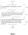
- FIG. 7is a process flow chart of an exemplary process for checking the integrity of configuration data by performing a cyclic redundancy check (CRC) of configuration data, according to one embodiment.
- the configuration dataare loaded to configuration registers of the programmable device.
- a master CRC datais accessed (e.g., from data supplied or based on a cyclic redundancy check applied to the configuration data).
- a current CRC data(e.g., through applying the cyclic redundancy check to current configuration data) is generated.
- the current CRC datais compared with the master CRC data. If there is mismatch, an event is generated in operation 710 . Otherwise, operations 704 , 706 , and 708 are repeated.
- redundancy checkother than the CRC may be performed on the configuration data.
- checksums, a horizontal redundancy check, a vertical redundancy check, and a cryptographic message digestmay be utilized to produce a similar result.
- a current RC datae.g., RC data based on current configuration data
- a master RC datae.g., RC data based on initial configuration data
- an exception eventmay be performed (e.g., such as communicating an interrupt data to a process of the programmable device or reloading the configuration registers with the initial configuration data).
- an exception eventmay be performed (e.g., such as communicating an interrupt data to a process of the programmable device or reloading the configuration registers with the initial configuration data).
- the checksums, horizontal redundancy check, vertical redundancy check, and cryptographic message digestare well-known to those skilled in the art of signal error detection.
- the programmable deviceincludes a microcontroller, a programmable logic device (PLD), a field programmable gate array (FPGA), and other types of programmable device.
- embodiments described hereinpertain to methods and systems of continuously checking the integrity of configuration data present in the configuration registers of a programmable device.
- the state of the configuration datamay be checked with the original configuration data stored to a different location.
- the DMA controller of the programmable devicemay enable to run the error-detection operation in background without sacrificing the performance of the programmable device.
Landscapes
- Engineering & Computer Science (AREA)
- Physics & Mathematics (AREA)
- General Physics & Mathematics (AREA)
- Theoretical Computer Science (AREA)
- Electromagnetism (AREA)
- Radar, Positioning & Navigation (AREA)
- Automation & Control Theory (AREA)
- General Engineering & Computer Science (AREA)
- Power Engineering (AREA)
- Signal Processing (AREA)
- Computer Security & Cryptography (AREA)
- Computer Networks & Wireless Communication (AREA)
- Power Sources (AREA)
- Continuous-Control Power Sources That Use Transistors (AREA)
- Semiconductor Integrated Circuits (AREA)
- Mobile Radio Communication Systems (AREA)
- Computer Hardware Design (AREA)
- Stored Programmes (AREA)
- Electronic Switches (AREA)
- Microcomputers (AREA)
Abstract
Description
Claims (18)
Priority Applications (2)
| Application Number | Priority Date | Filing Date | Title |
|---|---|---|---|
| US11/904,643US8125243B1 (en) | 2007-03-12 | 2007-09-28 | Integrity checking of configurable data of programmable device |
| US13/229,139US8766662B1 (en) | 2007-03-12 | 2011-09-09 | Integrity checking of configuration data of programmable device |
Applications Claiming Priority (2)
| Application Number | Priority Date | Filing Date | Title |
|---|---|---|---|
| US90660507P | 2007-03-12 | 2007-03-12 | |
| US11/904,643US8125243B1 (en) | 2007-03-12 | 2007-09-28 | Integrity checking of configurable data of programmable device |
Related Child Applications (1)
| Application Number | Title | Priority Date | Filing Date |
|---|---|---|---|
| US13/229,139ContinuationUS8766662B1 (en) | 2007-03-12 | 2011-09-09 | Integrity checking of configuration data of programmable device |
Publications (1)
| Publication Number | Publication Date |
|---|---|
| US8125243B1true US8125243B1 (en) | 2012-02-28 |
Family
ID=44906926
Family Applications (28)
| Application Number | Title | Priority Date | Filing Date |
|---|---|---|---|
| US11/904,644Active2028-09-12US8316158B1 (en) | 2007-03-12 | 2007-09-28 | Configuration of programmable device using a DMA controller |
| US11/904,643Active2028-01-27US8125243B1 (en) | 2007-03-12 | 2007-09-28 | Integrity checking of configurable data of programmable device |
| US11/973,090Active2028-07-19US8089306B1 (en) | 2007-03-12 | 2007-10-04 | Intelligent voltage regulator |
| US11/973,038Active2028-08-18US8072247B1 (en) | 2007-03-12 | 2007-10-04 | Programmable voltage regulator |
| US12/005,768Active2028-02-03US8058910B1 (en) | 2007-03-12 | 2007-12-27 | Intelligent power supervisor |
| US12/005,775ActiveUS8058911B1 (en) | 2007-03-12 | 2007-12-27 | Programmable power supervisor |
| US12/005,950Active2030-05-30US8060767B1 (en) | 2007-03-12 | 2007-12-28 | Ultra low power sleep mode |
| US12/075,632Active2028-12-15US8769177B1 (en) | 2007-03-12 | 2008-03-12 | Interrupt latency reduction |
| US12/075,633Active2029-11-24US8108529B1 (en) | 2007-03-12 | 2008-03-12 | Encoded acknowledge signal for wireless communication |
| US12/075,748Active2030-10-29US8280060B1 (en) | 2007-03-12 | 2008-03-12 | Secure wireless transmission |
| US13/167,006ActiveUS8179193B1 (en) | 2007-03-12 | 2011-06-23 | Intelligent voltage regulator |
| US13/182,264ActiveUS8269531B1 (en) | 2007-03-12 | 2011-07-13 | Programmable power supervisor |
| US13/182,295ActiveUS8471609B1 (en) | 2007-03-12 | 2011-07-13 | Intelligent power supervisor |
| US13/229,139Active2027-11-07US8766662B1 (en) | 2007-03-12 | 2011-09-09 | Integrity checking of configuration data of programmable device |
| US13/283,570ActiveUS8278978B1 (en) | 2007-03-12 | 2011-10-27 | Programmable voltage regulator |
| US13/296,977ActiveUS8510584B1 (en) | 2007-03-12 | 2011-11-15 | Ultra low power sleep mode |
| US13/466,004ActiveUS8786357B1 (en) | 2007-03-12 | 2012-05-07 | Intelligent voltage regulator |
| US13/610,623ActiveUS8680902B1 (en) | 2007-03-12 | 2012-09-11 | Programmable power supervisor |
| US13/633,696Expired - Fee RelatedUS8761397B1 (en) | 2007-03-12 | 2012-10-02 | Secure wireless transmission |
| US13/680,539ActiveUS8949478B2 (en) | 2007-03-12 | 2012-11-19 | Intelligent serial interface |
| US13/924,864ActiveUS9143027B2 (en) | 2007-03-12 | 2013-06-24 | Intelligent power supervisor |
| US14/310,530Active2028-03-07US9429964B2 (en) | 2007-03-12 | 2014-06-20 | Intelligent voltage regulator |
| US14/311,889ActiveUS9210571B1 (en) | 2007-03-12 | 2014-06-23 | Secure wireless communication |
| US14/319,041ActiveUS9588916B1 (en) | 2007-03-12 | 2014-06-30 | Interrupt latency reduction |
| US15/250,535ActiveUS10162774B2 (en) | 2007-03-12 | 2016-08-29 | Intelligent voltage regulator |
| US16/195,653ActiveUS10545519B2 (en) | 2007-03-12 | 2018-11-19 | Intelligent voltage regulator |
| US16/748,710ActiveUS10969806B2 (en) | 2007-03-12 | 2020-01-21 | Intelligent voltage regulator |
| US17/221,689ActiveUS11237578B2 (en) | 2007-03-12 | 2021-04-02 | Intelligent voltage regulator |
Family Applications Before (1)
| Application Number | Title | Priority Date | Filing Date |
|---|---|---|---|
| US11/904,644Active2028-09-12US8316158B1 (en) | 2007-03-12 | 2007-09-28 | Configuration of programmable device using a DMA controller |
Family Applications After (26)
| Application Number | Title | Priority Date | Filing Date |
|---|---|---|---|
| US11/973,090Active2028-07-19US8089306B1 (en) | 2007-03-12 | 2007-10-04 | Intelligent voltage regulator |
| US11/973,038Active2028-08-18US8072247B1 (en) | 2007-03-12 | 2007-10-04 | Programmable voltage regulator |
| US12/005,768Active2028-02-03US8058910B1 (en) | 2007-03-12 | 2007-12-27 | Intelligent power supervisor |
| US12/005,775ActiveUS8058911B1 (en) | 2007-03-12 | 2007-12-27 | Programmable power supervisor |
| US12/005,950Active2030-05-30US8060767B1 (en) | 2007-03-12 | 2007-12-28 | Ultra low power sleep mode |
| US12/075,632Active2028-12-15US8769177B1 (en) | 2007-03-12 | 2008-03-12 | Interrupt latency reduction |
| US12/075,633Active2029-11-24US8108529B1 (en) | 2007-03-12 | 2008-03-12 | Encoded acknowledge signal for wireless communication |
| US12/075,748Active2030-10-29US8280060B1 (en) | 2007-03-12 | 2008-03-12 | Secure wireless transmission |
| US13/167,006ActiveUS8179193B1 (en) | 2007-03-12 | 2011-06-23 | Intelligent voltage regulator |
| US13/182,264ActiveUS8269531B1 (en) | 2007-03-12 | 2011-07-13 | Programmable power supervisor |
| US13/182,295ActiveUS8471609B1 (en) | 2007-03-12 | 2011-07-13 | Intelligent power supervisor |
| US13/229,139Active2027-11-07US8766662B1 (en) | 2007-03-12 | 2011-09-09 | Integrity checking of configuration data of programmable device |
| US13/283,570ActiveUS8278978B1 (en) | 2007-03-12 | 2011-10-27 | Programmable voltage regulator |
| US13/296,977ActiveUS8510584B1 (en) | 2007-03-12 | 2011-11-15 | Ultra low power sleep mode |
| US13/466,004ActiveUS8786357B1 (en) | 2007-03-12 | 2012-05-07 | Intelligent voltage regulator |
| US13/610,623ActiveUS8680902B1 (en) | 2007-03-12 | 2012-09-11 | Programmable power supervisor |
| US13/633,696Expired - Fee RelatedUS8761397B1 (en) | 2007-03-12 | 2012-10-02 | Secure wireless transmission |
| US13/680,539ActiveUS8949478B2 (en) | 2007-03-12 | 2012-11-19 | Intelligent serial interface |
| US13/924,864ActiveUS9143027B2 (en) | 2007-03-12 | 2013-06-24 | Intelligent power supervisor |
| US14/310,530Active2028-03-07US9429964B2 (en) | 2007-03-12 | 2014-06-20 | Intelligent voltage regulator |
| US14/311,889ActiveUS9210571B1 (en) | 2007-03-12 | 2014-06-23 | Secure wireless communication |
| US14/319,041ActiveUS9588916B1 (en) | 2007-03-12 | 2014-06-30 | Interrupt latency reduction |
| US15/250,535ActiveUS10162774B2 (en) | 2007-03-12 | 2016-08-29 | Intelligent voltage regulator |
| US16/195,653ActiveUS10545519B2 (en) | 2007-03-12 | 2018-11-19 | Intelligent voltage regulator |
| US16/748,710ActiveUS10969806B2 (en) | 2007-03-12 | 2020-01-21 | Intelligent voltage regulator |
| US17/221,689ActiveUS11237578B2 (en) | 2007-03-12 | 2021-04-02 | Intelligent voltage regulator |
Country Status (1)
| Country | Link |
|---|---|
| US (28) | US8316158B1 (en) |
Cited By (7)
| Publication number | Priority date | Publication date | Assignee | Title |
|---|---|---|---|---|
| US20110231636A1 (en)* | 2010-03-16 | 2011-09-22 | Olson Christopher H | Apparatus and method for implementing instruction support for performing a cyclic redundancy check (crc) |
| US8598908B1 (en)* | 2009-05-01 | 2013-12-03 | Cypress Semiconductor Corp. | Built in system bus interface for random access to programmable logic registers |
| US8766662B1 (en)* | 2007-03-12 | 2014-07-01 | Cypress Semiconductor Corporation | Integrity checking of configuration data of programmable device |
| WO2014137939A1 (en)* | 2013-03-04 | 2014-09-12 | Amazon Technologies, Inc. | Configuration and verification by trusted provider |
| US10345377B2 (en)* | 2009-05-05 | 2019-07-09 | Cypress Semiconductor Corporation | Combined analog architecture and functionality in a mixed-signal array |
| US10666258B2 (en) | 2009-05-05 | 2020-05-26 | Cypress Semiconductor Corporation | Programmable input/output circuit |
| US11018693B2 (en)* | 2018-07-12 | 2021-05-25 | Maxim Integrated Products, Inc. | System and method for continuously verifying device state integrity |
Families Citing this family (85)
| Publication number | Priority date | Publication date | Assignee | Title |
|---|---|---|---|---|
| US9413233B2 (en)* | 2005-10-24 | 2016-08-09 | Parkervision, Inc. | Switching power supply with dynamically programmed threshold voltage |
| US10684974B1 (en)* | 2007-03-12 | 2020-06-16 | Cypress Semiconductor Corporation | Auto-switching communication interface |
| US8288971B2 (en)* | 2008-01-11 | 2012-10-16 | Broadcom Corporation | Integrated and programmable microphone bias generation |
| US8307180B2 (en) | 2008-02-28 | 2012-11-06 | Nokia Corporation | Extended utilization area for a memory device |
| US8812641B2 (en)* | 2008-09-30 | 2014-08-19 | Freescale Semiconductor, Inc. | Processing load with normal or fast operation mode |
| DE102008053536B4 (en)* | 2008-10-28 | 2011-12-01 | Atmel Automotive Gmbh | Circuit, use and method of operating a circuit |
| US8155766B2 (en)* | 2008-11-03 | 2012-04-10 | Hitachi, Ltd. | Methods and apparatus to provision power-saving storage system |
| US8874824B2 (en) | 2009-06-04 | 2014-10-28 | Memory Technologies, LLC | Apparatus and method to share host system RAM with mass storage memory RAM |
| CN102204364B (en)* | 2011-04-26 | 2013-01-16 | 华为终端有限公司 | Method and server for processing service |
| KR101789225B1 (en) | 2011-06-23 | 2017-11-20 | 삼성전자주식회사 | Device and signal processing method thereof |
| US8972763B2 (en)* | 2011-12-05 | 2015-03-03 | Intel Corporation | Method, apparatus, and system for energy efficiency and energy conservation including determining an optimal power state of the apparatus based on residency time of non-core domains in a power saving state |
| DE102012205160A1 (en)* | 2012-03-29 | 2013-10-02 | Robert Bosch Gmbh | Communication arrangement and method for configuring programmable hardware |
| KR101970314B1 (en)* | 2012-04-10 | 2019-04-18 | 삼성전자주식회사 | Non-volatile memory device, operating method thereof, and electronic device having the same |
| US9311226B2 (en)* | 2012-04-20 | 2016-04-12 | Memory Technologies Llc | Managing operational state data of a memory module using host memory in association with state change |
| US9213381B2 (en)* | 2012-05-24 | 2015-12-15 | Ati Technologies Ulc | Voltage regulator dynamically determining whether requested power transition can be supported |
| US8959274B2 (en)* | 2012-09-06 | 2015-02-17 | Silicon Laboratories Inc. | Providing a serial download path to devices |
| TWI503644B (en)* | 2012-10-05 | 2015-10-11 | Faraday Tech Corp | Calibration circuit for a voltage regulator |
| BR112015010329B1 (en) | 2012-11-07 | 2020-12-08 | The Lubrizol Corporation | basic additives without ash |
| US20140149773A1 (en)* | 2012-11-29 | 2014-05-29 | Agency For Science, Technology And Research | Latch circuit and data processing system |
| US9678564B2 (en)* | 2012-12-21 | 2017-06-13 | Nxp B.V. | Multiprocessor system with interrupt distributor |
| US9330027B2 (en) | 2013-03-15 | 2016-05-03 | Intel Corporation | Register access white listing |
| CN103218968B (en)* | 2013-04-27 | 2016-04-06 | 合肥京东方光电科技有限公司 | Gamma resistance adjusting gear, driving circuit and display device |
| EP2806548B1 (en)* | 2013-05-24 | 2020-07-22 | EM Microelectronic-Marin SA | Voltage regulator |
| US9383802B1 (en)* | 2013-06-20 | 2016-07-05 | Altera Corporation | Integrated circuit with state and data retention |
| JP6122720B2 (en)* | 2013-07-17 | 2017-04-26 | ルネサスエレクトロニクス株式会社 | Power supply voltage transition verification circuit, power supply voltage transition verification method, and semiconductor integrated circuit |
| EP2926214B1 (en)* | 2013-09-04 | 2017-04-12 | IDT Europe GmbH | Fpga power management system |
| FR3012273A1 (en)* | 2013-10-22 | 2015-04-24 | St Microelectronics Sa | |
| JP6232925B2 (en)* | 2013-10-28 | 2017-11-22 | 富士電機株式会社 | Input circuit |
| KR102042506B1 (en)* | 2013-10-31 | 2019-11-11 | 한국전자통신연구원 | Wheel speed sensor interface, operation method thereof, and electronic control system including the same |
| CN103676739B (en)* | 2013-12-05 | 2016-06-01 | 上海交通大学 | A kind of DMA data transmission system based on embedded motion control board card and transmission method thereof |
| US20150316971A1 (en)* | 2014-05-02 | 2015-11-05 | Avalanche Technology, Inc. | Method and apparatus to reduce power consumption of mobile and portable devices with non-volatile memories |
| US10691838B2 (en)* | 2014-06-20 | 2020-06-23 | Cypress Semiconductor Corporation | Encryption for XIP and MMIO external memories |
| JP6455132B2 (en)* | 2014-12-22 | 2019-01-23 | 富士通株式会社 | Information processing apparatus, processing method, and program |
| US10095435B1 (en) | 2015-01-09 | 2018-10-09 | Altera Corporation | Methods for initializing memory devices |
| WO2016122513A1 (en)* | 2015-01-29 | 2016-08-04 | Hewlett Packard Enterprise Development Lp | Data analytics on encrypted data elements |
| US9689582B2 (en) | 2015-04-10 | 2017-06-27 | Lennox Industries Inc. | Overvoltage recovery circuit and a controller and HVAC system including the same |
| US9660659B2 (en)* | 2015-05-13 | 2017-05-23 | Sk Hynix Memory Solutions Inc. | Apparatus for correcting gain error of analog-to-digital converter |
| JP6578757B2 (en)* | 2015-06-23 | 2019-09-25 | セイコーエプソン株式会社 | Power supply voltage detection circuit, semiconductor integrated circuit device, and electronic device |
| US10398359B2 (en) | 2015-07-13 | 2019-09-03 | BioMetrix LLC | Movement analysis system, wearable movement tracking sensors, and associated methods |
| US10263968B1 (en)* | 2015-07-24 | 2019-04-16 | Hologic Inc. | Security measure for exchanging keys over networks |
| CN105068800B (en)* | 2015-07-31 | 2018-09-14 | 深圳市华星光电技术有限公司 | A kind of method of download configuration code, system and timer/counter control register |
| US10795391B2 (en)* | 2015-09-04 | 2020-10-06 | Texas Instruments Incorporated | Voltage regulator wake-up |
| US9990316B2 (en) | 2015-09-21 | 2018-06-05 | Qualcomm Incorporated | Enhanced serial peripheral interface |
| US9836071B2 (en) | 2015-12-29 | 2017-12-05 | Silicon Laboratories Inc. | Apparatus for multiple-input power architecture for electronic circuitry and associated methods |
| US9964986B2 (en)* | 2015-12-29 | 2018-05-08 | Silicon Laboratories Inc. | Apparatus for power regulator with multiple inputs and associated methods |
| JP6606038B2 (en)* | 2016-09-06 | 2019-11-13 | 株式会社東芝 | Output voltage control circuit |
| US10057061B1 (en)* | 2016-09-13 | 2018-08-21 | Wells Fargo Bank, N.A. | Secure digital communications |
| US10075300B1 (en) | 2016-09-13 | 2018-09-11 | Wells Fargo Bank, N.A. | Secure digital communications |
| US10650727B2 (en)* | 2016-10-04 | 2020-05-12 | Semiconductor Energy Laboratory Co., Ltd. | Semiconductor device, display device, and electronic device |
| US10853798B1 (en) | 2016-11-28 | 2020-12-01 | Wells Fargo Bank, N.A. | Secure wallet-to-wallet transactions |
| US10613604B2 (en)* | 2016-12-22 | 2020-04-07 | Texas Instruments Incorporated | On chip power on reset with integrated supervisory functions for a functional safety system |
| US10057225B1 (en) | 2016-12-29 | 2018-08-21 | Wells Fargo Bank, N.A. | Wireless peer to peer mobile wallet connections |
| US10228736B2 (en)* | 2016-12-30 | 2019-03-12 | Texas Instruments Incorporated | Reset isolation for an embedded safety island in a system on a chip |
| US10162373B1 (en)* | 2017-02-28 | 2018-12-25 | Ampere Computing Llc | Variation immune on-die voltage droop detector |
| TWI654871B (en)* | 2017-04-05 | 2019-03-21 | 立積電子股份有限公司 | Power control circuit and method thereof |
| US10222402B2 (en) | 2017-05-18 | 2019-03-05 | Cypress Semiconductor Corporation | Current sensing in a USB power control analog subsystem |
| US10228742B2 (en)* | 2017-05-18 | 2019-03-12 | Cypress Semiconductor Corporation | USB power control analog subsystem architecture |
| KR102324194B1 (en)* | 2017-05-22 | 2021-11-10 | 삼성전자주식회사 | Voltage trimming circuit including anti-fuses, operating method thereof, and integrated circuit having the voltage trimming circuit |
| US10776777B1 (en) | 2017-08-04 | 2020-09-15 | Wells Fargo Bank, N.A. | Consolidating application access in a mobile wallet |
| KR101937268B1 (en)* | 2017-10-11 | 2019-04-09 | 현대오트론 주식회사 | Real-time slope control appartus for voltage regulator and operating method thereof |
| CN107832249B (en)* | 2017-10-29 | 2020-07-03 | 北京联合大学 | System and method for three-wire communication with peripheral devices with SPI interface |
| DE102018200704B4 (en) | 2018-01-17 | 2022-02-10 | Robert Bosch Gmbh | Electrical circuit for the safe acceleration and deceleration of a consumer |
| CN108646834A (en)* | 2018-03-22 | 2018-10-12 | 芯海科技(深圳)股份有限公司 | A kind of low cost low-power consumption method of supplying power to for reducing numeric field and high-precision adc being interfered |
| US10866606B2 (en)* | 2018-03-28 | 2020-12-15 | Qualcomm Incorporated | Methods and apparatuses for multiple-mode low drop out regulators |
| US11218071B2 (en) | 2018-04-30 | 2022-01-04 | Hewlett-Packard Development Company, L.P. | Isolating electrical components |
| US10468089B1 (en)* | 2018-06-04 | 2019-11-05 | Nanya Technology Corporation | Voltage-stabilizing circuit, DRAM, and method for stabilizing a bit line voltage |
| US11442886B2 (en)* | 2018-06-08 | 2022-09-13 | IOT.nxt BV | Communication apparatus capable of implementing a selected communication protocol |
| TWI664811B (en)* | 2018-12-14 | 2019-07-01 | Giga-Byte Technology Co.,Ltd. | Power regulator and power regulating method |
| US12132810B2 (en)* | 2018-12-18 | 2024-10-29 | Texas Instruments Incorporated | Protocol auto-detection |
| JP7151539B2 (en)* | 2019-02-21 | 2022-10-12 | セイコーエプソン株式会社 | Real-time clock modules, electronic devices, and moving objects |
| EP3702947B1 (en)* | 2019-03-01 | 2021-10-20 | Siemens Aktiengesellschaft | Method for verifying at runtime of a hardware-application component a current configuration setting of an execution environment provided by a configurable hardware module |
| KR102735222B1 (en) | 2020-01-30 | 2024-11-27 | 삼성전자주식회사 | Supply voltage detecting circuit, electronic device comprising same and electronic system comprising same |
| US11200001B2 (en)* | 2020-05-15 | 2021-12-14 | Micron Technology, Inc. | Management of power during memory device reset and initialization |
| US11221667B1 (en)* | 2020-07-30 | 2022-01-11 | Qualcomm Incorporated | Dynamic voltage selection for a single power rail in a multi-core domain |
| FR3113746B1 (en)* | 2020-08-27 | 2022-07-29 | St Microelectronics Rousset | Integrated circuit, reset method and computer program product |
| KR102835998B1 (en)* | 2020-09-22 | 2025-07-18 | 에스케이하이닉스 주식회사 | Voltage generation circuit, semiconductor apparatus including the voltage generation circuit and voltage offset calibration system |
| IT202100015197A1 (en)* | 2021-06-10 | 2022-12-10 | St Microelectronics Rousset | Corresponding power circuit, device and method |
| IT202100015176A1 (en) | 2021-06-10 | 2022-12-10 | St Microelectronics Srl | Corresponding power circuit, device and method |
| US11853148B2 (en) | 2021-09-23 | 2023-12-26 | Apple Inc. | Datalogging circuit triggered by a watchdog timer |
| CN114024429B (en)* | 2021-10-27 | 2024-02-20 | 成都芯源系统有限公司 | Power chip with multiplexed pins |
| US11601123B1 (en) | 2021-11-10 | 2023-03-07 | Nxp B.V. | Power-on reset (POR) circuit |
| CN117178264A (en)* | 2022-03-21 | 2023-12-05 | 梦芯片技术股份有限公司 | data storage circuit |
| TWI855654B (en)* | 2023-04-26 | 2024-09-11 | 大陸商星宸科技股份有限公司 | Voltage detector device having trimming mechanism and voltage detection method |
| US12341497B2 (en)* | 2023-06-23 | 2025-06-24 | Qualcomm Incorporated | Power multiplexer |
| US20250156329A1 (en)* | 2023-11-13 | 2025-05-15 | Advanced Micro Devices, Inc. | Prefetching using a direct memory access engine |
Citations (80)
| Publication number | Priority date | Publication date | Assignee | Title |
|---|---|---|---|---|
| US4727514A (en) | 1986-02-11 | 1988-02-23 | Texas Instruments Incorporated | Programmable memory with memory cells programmed by addressing |
| US4734885A (en) | 1985-10-17 | 1988-03-29 | Harris Corporation | Programming arrangement for programmable devices |
| US5163146A (en) | 1988-10-14 | 1992-11-10 | International Business Machines Corporation | System responsive to interrupt levels for changing and restoring clock speed by changing and restoring a register value |
| US5336951A (en) | 1991-05-03 | 1994-08-09 | Lattice Semiconductor Corporation | Structure and method for multiplexing pins for in-system programming |
| EP0619548A1 (en) | 1993-04-06 | 1994-10-12 | STMicroelectronics S.r.l. | Interface circuit between a control bus and an integrated circuit suitable for two different protocol standards |
| US5369703A (en) | 1993-06-03 | 1994-11-29 | At&T Corp. | Command and control signalling method and apparatus |
| US5376834A (en) | 1993-03-05 | 1994-12-27 | Sgs-Thomson Microelectronics, Inc. | Initialization circuit for automatically establishing an output to zero or desired reference potential |
| US5481549A (en) | 1987-04-30 | 1996-01-02 | Fujitsu Limited | Apparatus for testing an integrated circuit in which an input test pattern can be changed with an selected application timing |
| US5568083A (en) | 1993-07-02 | 1996-10-22 | Hitachi, Ltd. | Semiconductor integrated circuit device having an internally produced operation voltage matched to operation speed of circuit |
| US5594442A (en) | 1994-03-15 | 1997-01-14 | Crystal Semiconductor Corporation | Configuration programming of a digital audio serial port using no additional pins |
| US5629635A (en) | 1995-09-26 | 1997-05-13 | Ics Technologies, Inc. | Address programming via LED pin |
| US5661685A (en) | 1995-09-25 | 1997-08-26 | Xilinx, Inc. | Programmable logic device with configurable power supply |
| US5664205A (en) | 1993-11-23 | 1997-09-02 | Advanced Micro Devices, Inc. | Power management control technique for timer tick activity within an interrupt driven computer system |
| US5693570A (en) | 1994-10-17 | 1997-12-02 | Sandisk Corporation | Process for manufacturing a programmable power generation circuit for flash EEPROM memory systems |
| US5726995A (en) | 1994-12-15 | 1998-03-10 | Intel Corporation | Method and apparatus for selecting modes of an intergrated circuit |
| US5748684A (en) | 1992-03-18 | 1998-05-05 | Crystal Semiconductor, Inc. | Resynchronization of a synchronous serial interface |
| US5838950A (en) | 1992-10-15 | 1998-11-17 | Adaptec, Inc. | Method of operation of a host adapter integrated circuit |
| US5877719A (en) | 1997-02-24 | 1999-03-02 | Mitsubishi Electric Engineering Co., Ltd. | Method of controlling analog-to-digital converter |
| US5878234A (en) | 1996-09-10 | 1999-03-02 | Sierra Wireless, Inc. | Low power serial protocol translator for use in multi-circuit board electronic systems |
| US5925110A (en) | 1997-01-07 | 1999-07-20 | Micron Electronics, Inc. | Low power keyboard with power supply switch that is activated by receiver output to power up and down keyboard components including microcontroller demodulator |
| US6038400A (en) | 1995-09-27 | 2000-03-14 | Linear Technology Corporation | Self-configuring interface circuitry, including circuitry for identifying a protocol used to send signals to the interface circuitry, and circuitry for receiving the signals using the identified protocol |
| US6105155A (en) | 1998-01-21 | 2000-08-15 | International Business Machines Corporation | Method and apparatus for performing on-chip function checks and locating detected anomalies within a nested time interval using CRCs or the like |
| US6182163B1 (en) | 1995-05-26 | 2001-01-30 | Mitsubishi Denki Kabushiki Kaisha | Control method for distributed type remote I/O control system performing automatic reset of output at start if no detected transmissions in specific period |
| US6191614B1 (en)* | 1999-04-05 | 2001-02-20 | Xilinx, Inc. | FPGA configuration circuit including bus-based CRC register |
| US6195792B1 (en) | 1998-02-19 | 2001-02-27 | Nortel Networks Limited | Software upgrades by conversion automation |
| US6253268B1 (en) | 1999-01-15 | 2001-06-26 | Telefonaktiebolaget L M Ericsson (Publ) | Method and system for multiplexing a second interface on an I2C interface |
| US6256240B1 (en) | 1998-11-09 | 2001-07-03 | Fujitsu Limited | Semiconductor memory circuit |
| US6260139B1 (en) | 1999-01-26 | 2001-07-10 | Xilinx, Inc. | FPGA control structure for self-reconfiguration |
| US6281716B1 (en) | 1998-07-01 | 2001-08-28 | Mitsubishi Denki Kabushiki Kaisha | Potential detect circuit for detecting whether output potential of potential generation circuit has arrived at target potential or not |
| US6320809B1 (en) | 2000-07-05 | 2001-11-20 | Micron Technology, Inc. | Low voltage level power-up detection circuit |
| US6330231B1 (en) | 1995-10-16 | 2001-12-11 | Nec Corporation | Dynamic server allocation for load balancing wireless remote interface processing |
| US6400605B1 (en) | 2000-05-30 | 2002-06-04 | Summit Microelectronics, Inc. | Method and system for pulse shaping in test and program modes |
| US6429682B1 (en)* | 1999-04-05 | 2002-08-06 | Xilinx, Inc. | Configuration bus interface circuit for FPGAs |
| US20020108011A1 (en) | 2000-12-11 | 2002-08-08 | Reza Tanha | Dual interface serial bus |
| US6499123B1 (en) | 1989-02-24 | 2002-12-24 | Advanced Micro Devices, Inc. | Method and apparatus for debugging an integrated circuit |
| US6509845B1 (en) | 1999-03-08 | 2003-01-21 | Sharp Kabushiki Kaisha | Wireless input apparatus |
| US20030074364A1 (en) | 2001-10-12 | 2003-04-17 | Sewall Patrick M. | Compressed data structure and decompression system |
| US20030093751A1 (en)* | 2001-11-09 | 2003-05-15 | David Hohl | System and method for fast cyclic redundancy calculation |
| US6577157B1 (en) | 1997-11-14 | 2003-06-10 | Altera Corporation | Fully programmable I/O pin with memory |
| US6577175B2 (en) | 2001-06-01 | 2003-06-10 | Samsung Electronics Co., Ltd. | Method for generating internal clock of semiconductor memory device and circuit thereof |
| US6798254B2 (en) | 2001-08-03 | 2004-09-28 | Hewlett-Packard Development Company, L.P. | Dynamic control of switching reference voltage |
| US6865113B2 (en) | 2003-07-23 | 2005-03-08 | Catalyst Semiconductor, Inc. | System and method for programming non-volatile memory |
| US20050052437A1 (en) | 2002-08-14 | 2005-03-10 | Elcos Microdisplay Technology, Inc. | Temperature sensor circuit for microdisplays |
| US20050071730A1 (en)* | 2003-09-30 | 2005-03-31 | Lattice Semiconductor Corporation | Continuous self-verify of configuration memory in programmable logic devices |
| US20050093572A1 (en)* | 2003-11-03 | 2005-05-05 | Macronix International Co., Ltd. | In-circuit configuration architecture with configuration on initialization function for embedded configurable logic array |
| US20050093582A1 (en)* | 2003-10-29 | 2005-05-05 | Andreas Bock | Integrated loss of signal detection with wide threshold range and precise hysteresis |
| US6912606B2 (en) | 2001-06-08 | 2005-06-28 | Sycamore Networks, Inc. | Generic serial bus architecture |
| US6924790B1 (en) | 1995-10-16 | 2005-08-02 | Nec Corporation | Mode switching for pen-based computer systems |
| US6999342B2 (en) | 2002-10-08 | 2006-02-14 | Renesas Technology Corp. | Semiconductor device saving data in non-volatile manner during standby |
| US20060035590A1 (en) | 2004-03-16 | 2006-02-16 | Morris Martin G | High-reliability computer interface for wireless input devices |
| US7030668B1 (en) | 2003-06-24 | 2006-04-18 | Xilinx, Inc. | Voltage detector |
| US7089434B2 (en) | 2003-06-24 | 2006-08-08 | Lite-On Technology Corporation | Wireless signal receiving device with prompt wake-up function |
| US7096137B2 (en) | 2002-12-02 | 2006-08-22 | Silverbrook Research Pty Ltd | Clock trim mechanism for onboard system clock |
| US7107178B2 (en) | 2003-10-06 | 2006-09-12 | Samsung Electronics Co., Ltd. | Temperature sensing circuit for use in semiconductor integrated circuit |
| US20060212838A1 (en) | 2005-02-09 | 2006-09-21 | Checksum, Llc | System and apparatus for in-system programming |
| US20060236147A1 (en) | 2005-04-15 | 2006-10-19 | Rambus Inc. | Processor controlled interface |
| US7174144B2 (en) | 2002-09-13 | 2007-02-06 | Broadcom Corporation | Calibration of a phase locked loop |
| US20070094420A1 (en)* | 2005-10-18 | 2007-04-26 | Ingemar Holm | System and method for validating chip configuration data |
| US7228476B2 (en) | 2004-11-05 | 2007-06-05 | Stmicroelectronics, Inc. | System and method for testing integrated circuits at operational speed using high-frequency clock converter |
| US20070183205A1 (en) | 2006-02-03 | 2007-08-09 | Samsung Electronics Co., Ltd. | Semiconductor memory device controlling program voltage according to the number of cells to be programmed and method of programming the same |
| US7269780B2 (en) | 2002-10-02 | 2007-09-11 | Matsushita Electric Industrial Co., Ltd. | Power management for circuits with inactive state data save and restore scan chain |
| US7304923B2 (en) | 2002-10-10 | 2007-12-04 | Sony Corporation | Disk drive and detection method using pre-pit detection and push-pull signal generation |
| US7310757B2 (en)* | 2001-10-11 | 2007-12-18 | Altera Corporation | Error detection on programmable logic resources |
| US20080071972A1 (en) | 2006-09-13 | 2008-03-20 | Rohm Co., Ltd. | Data Processing Apparatus And Data Control Circuit For Use Therein |
| US20080086626A1 (en) | 2006-10-05 | 2008-04-10 | Simon Jones | Inter-processor communication method |
| US7385418B2 (en)* | 2003-07-31 | 2008-06-10 | Actel Corporation | Non-volatile memory architecture for programmable-logic-based system on a chip |
| US7392447B2 (en) | 2004-10-25 | 2008-06-24 | Princeton Technology Corporation | Method of using scan chains and boundary scan for power saving |
| US7392409B2 (en) | 2001-08-01 | 2008-06-24 | Canon Kabushiki Kaisha | Data processing apparatus and power control method |
| US7415647B2 (en) | 2006-04-06 | 2008-08-19 | Micrel, Incorporated | Test mode for pin-limited devices |
| US7415624B2 (en) | 2004-04-06 | 2008-08-19 | Cisco Technology, Inc. | System and method for saving power in a wireless network by reducing power to a wireless station for a time interval if a received packet fails an integrity check |
| US7421291B2 (en) | 2002-08-12 | 2008-09-02 | Broadcom Corporation | Method for selective power management for a hand held host |
| US7508242B2 (en) | 2006-03-31 | 2009-03-24 | Oki Semiconductor Co., Ltd. | Driving circuit that eliminates effects of ambient temperature variations and increases driving capacity |
| US7532056B2 (en) | 2005-08-10 | 2009-05-12 | Samsung Electronics Co., Ltd. | On chip temperature detector, temperature detection method and refresh control method using the same |
| US20090167093A1 (en) | 2007-12-28 | 2009-07-02 | Sandisk Corporation | Systems and Circuits with Multirange and Localized Detection of Valid Power |
| US20090315582A1 (en) | 2006-03-02 | 2009-12-24 | Denso Corporation | Test mode enable circuit |
| US7672258B1 (en) | 2004-09-24 | 2010-03-02 | Nortel Networks Limited | Signalling channel and radio system for power saving in wireless devices |
| US7710939B2 (en) | 2007-02-06 | 2010-05-04 | Samsung Electronics Co., Ltd. | Method and system for power saving in wireless local area communication networks |
| US7739529B2 (en) | 2000-07-26 | 2010-06-15 | Bridgestone Americas Tire Operations, Llc | System for conserving battery life in a battery operated device |
| US7760655B2 (en) | 2005-12-27 | 2010-07-20 | Oce Printing Systems Gmbh | Method and device for transfer of data over a data connection from a sender to a receiver by means of packets |
| US7844308B2 (en) | 2005-06-01 | 2010-11-30 | Millennial Net, Inc. | Communicating over a wireless network |
Family Cites Families (124)
| Publication number | Priority date | Publication date | Assignee | Title |
|---|---|---|---|---|
| US3932261A (en) | 1974-06-24 | 1976-01-13 | Olin Corporation | Electrode assembly for an electrolytic cell |
| US4908188A (en)* | 1985-02-05 | 1990-03-13 | The Scopas Technology Company, Inc. | Gas sterilant system |
| US4668932A (en) | 1985-07-26 | 1987-05-26 | Xicor, Inc. | Nonvolatile reprogrammable electronic potentiometer |
| US4656553A (en) | 1986-01-21 | 1987-04-07 | Comair Rotron, Inc. | Electronically programmable universal brushless DC fan with integral tracking and locked rotor protection |
| JP2577897B2 (en) | 1986-10-31 | 1997-02-05 | 日本テキサス・インスツルメンツ 株式会社 | Constant voltage power supply circuit |
| US5006974A (en)* | 1987-12-24 | 1991-04-09 | Waferscale Integration Inc. | On-chip high voltage generator and regulator in an integrated circuit |
| US5014097A (en)* | 1987-12-24 | 1991-05-07 | Waferscale Integration, Inc. | On-chip high voltage generator and regulator in an integrated circuit |
| JPH01214993A (en) | 1988-02-23 | 1989-08-29 | Nissan Motor Co Ltd | data storage device |
| JP2769478B2 (en) | 1989-04-10 | 1998-06-25 | 三菱電機株式会社 | transceiver |
| JP2762670B2 (en) | 1990-03-30 | 1998-06-04 | 松下電器産業株式会社 | Data processing device |
| JP2507833B2 (en)* | 1990-12-25 | 1996-06-19 | 三菱電機株式会社 | Micro computer |
| FR2681180B1 (en)* | 1991-09-05 | 1996-10-25 | Gemplus Card Int | PROGRAMMING VOLTAGE REGULATION CIRCUIT FOR PROGRAMMABLE MEMORIES. |
| JPH05108191A (en)* | 1991-10-11 | 1993-04-30 | Toshiba Corp | Portable computer |
| US5336986A (en)* | 1992-02-07 | 1994-08-09 | Crosspoint Solutions, Inc. | Voltage regulator for field programmable gate arrays |
| US5546568A (en)* | 1993-12-29 | 1996-08-13 | Intel Corporation | CPU clock control unit |
| JP3705842B2 (en)* | 1994-08-04 | 2005-10-12 | 株式会社ルネサステクノロジ | Semiconductor device |
| US5644772A (en)* | 1994-08-12 | 1997-07-01 | Advanced Micro Devices, Inc. | Signal dispatching for C language interrupt handling |
| US5671149A (en)* | 1995-01-11 | 1997-09-23 | Dell Usa, L.P. | Programmable board mounted voltage regulators |
| JPH08298462A (en) | 1995-04-27 | 1996-11-12 | Nec Corp | Semiconductor device |
| US5966529A (en)* | 1995-05-15 | 1999-10-12 | Zsp Corporation | Processor having auxiliary operand register file and complementary arrangements for non-disruptively performing adjunct execution |
| US5581206A (en) | 1995-07-28 | 1996-12-03 | Micron Quantum Devices, Inc. | Power level detection circuit |
| JP3124230B2 (en)* | 1995-08-11 | 2001-01-15 | 株式会社沖データ | Drive |
| US6341324B1 (en)* | 1995-10-06 | 2002-01-22 | Lsi Logic Corporation | Exception processing in superscalar microprocessor |
| US5596532A (en) | 1995-10-18 | 1997-01-21 | Sandisk Corporation | Flash EEPROM self-adaptive voltage generation circuit operative within a continuous voltage source range |
| US5744944A (en)* | 1995-12-13 | 1998-04-28 | Sgs-Thomson Microelectronics, Inc. | Programmable bandwidth voltage regulator |
| US5764529A (en)* | 1996-12-23 | 1998-06-09 | International Business Machines Corporation | Method and apparatus for automatic frequency and voltage selection for microprocessors |
| US5987601A (en)* | 1997-02-14 | 1999-11-16 | Xyron Corporation | Zero overhead computer interrupts with task switching |
| US6144374A (en)* | 1997-05-15 | 2000-11-07 | Orion Electric Co., Ltd. | Apparatus for driving a flat panel display |
| US6195712B1 (en) | 1997-06-13 | 2001-02-27 | Intel Corporation | Dynamic discovery of wireless peripherals |
| US5982241A (en)* | 1997-07-31 | 1999-11-09 | Dallas Semiconductor Corporation | Monolithic oscillator utilizing frequency-locked loop feedback network |
| US5963105A (en)* | 1997-07-31 | 1999-10-05 | Dallas Semiconductor Corporation | Trimmable circuitry for providing compensation for the temperature coefficients of a voltage controlled crystal-less oscillator |
| US5987495A (en)* | 1997-11-07 | 1999-11-16 | International Business Machines Corporation | Method and apparatus for fully restoring a program context following an interrupt |
| JPH11273360A (en) | 1998-03-17 | 1999-10-08 | Toshiba Corp | Ferroelectric memory device |
| US6603280B2 (en) | 1998-04-02 | 2003-08-05 | Hitachi, Ltd. | Motor controller |
| US6232893B1 (en)* | 1998-05-27 | 2001-05-15 | Altera Corporation | Method and apparatus for programmably providing a power supply voltage to an integrated circuit |
| KR100289846B1 (en)* | 1998-09-29 | 2001-05-15 | 윤종용 | Low power consumption voltage controller |
| US6298448B1 (en) | 1998-12-21 | 2001-10-02 | Siemens Information And Communication Networks, Inc. | Apparatus and method for automatic CPU speed control based on application-specific criteria |
| JP3942765B2 (en)* | 1999-03-15 | 2007-07-11 | 株式会社アドバンテスト | Semiconductor device simulation apparatus and program debugging apparatus for semiconductor test using the same |
| US6316988B1 (en) | 1999-03-26 | 2001-11-13 | Seagate Technology Llc | Voltage margin testing using an embedded programmable voltage source |
| US6137188A (en) | 1999-05-28 | 2000-10-24 | 3Com Corporation | Method for shared voltage regulation with multiple devices |
| PL194385B1 (en) | 1999-09-01 | 2007-05-31 | Pilkington Plc | Improvements in or relating to tempered glazings, and glass for use therein |
| US6321282B1 (en) | 1999-10-19 | 2001-11-20 | Rambus Inc. | Apparatus and method for topography dependent signaling |
| TW463080B (en) | 2000-03-24 | 2001-11-11 | Winbond Electronics Corp | Clock generating device which can adjust clock skew and method |
| US6684342B1 (en)* | 2000-06-22 | 2004-01-27 | Ubicom, Inc. | Apparatus and method of dynamic and deterministic changes in clock frequency for lower power consumption while maintaining fast interrupt handling |
| US6785829B1 (en)* | 2000-06-30 | 2004-08-31 | Intel Corporation | Multiple operating frequencies in a processor |
| US6798299B1 (en)* | 2000-10-26 | 2004-09-28 | Cypress Semiconductor Corporation | Crystal-less oscillator circuit with trimmable analog current control for increased stability |
| US8176296B2 (en)* | 2000-10-26 | 2012-05-08 | Cypress Semiconductor Corporation | Programmable microcontroller architecture |
| US6854067B1 (en) | 2000-10-30 | 2005-02-08 | Cypress Semiconductor Corporation | Method and system for interaction between a processor and a power on reset circuit to dynamically control power states in a microcontroller |
| US6832273B2 (en)* | 2000-12-21 | 2004-12-14 | Microsoft Corporation | System and method to specify extended configuration descriptor information in USB devices |
| US7127678B2 (en)* | 2000-12-21 | 2006-10-24 | Microsoft Corporation | System and method to specify device specific user interface information in the firmware of a USB device |
| US7224801B2 (en) | 2000-12-27 | 2007-05-29 | Logitech Europe S.A. | Wireless secure device |
| US7146532B2 (en) | 2001-02-05 | 2006-12-05 | Affiniti, Inc. | Persistent session and data in transparently distributed objects |
| JP2002366112A (en) | 2001-06-07 | 2002-12-20 | Hitachi Ltd | Liquid crystal driving device and liquid crystal display device |
| US20040218762A1 (en)* | 2003-04-29 | 2004-11-04 | Eric Le Saint | Universal secure messaging for cryptographic modules |
| DE60204189T2 (en)* | 2001-06-29 | 2006-02-02 | Stmicroelectronics Pvt. Ltd. | FPGA with at least two different and independently configurable memory structures |
| JP2003116070A (en)* | 2001-08-01 | 2003-04-18 | Sanyo Electric Co Ltd | Picture signal processing device |
| JP4727860B2 (en)* | 2001-08-03 | 2011-07-20 | 富士通株式会社 | Wireless operation device and program |
| US7983419B2 (en) | 2001-08-09 | 2011-07-19 | Trimble Navigation Limited | Wireless device to network server encryption |
| US6456557B1 (en)* | 2001-08-28 | 2002-09-24 | Tower Semiconductor Ltd | Voltage regulator for memory device |
| US6983376B2 (en)* | 2001-10-16 | 2006-01-03 | Qualcomm Incorporated | Method and apparatus for providing privacy of user identity and characteristics in a communication system |
| DE60141467D1 (en)* | 2001-11-15 | 2010-04-15 | Texas Instruments Inc | Interruptable and resumable instruction for cleaning a segment of a cache memory |
| JP2003173674A (en) | 2001-12-03 | 2003-06-20 | Matsushita Electric Ind Co Ltd | Voltage detection level correction circuit and semiconductor device |
| US20030120922A1 (en)* | 2001-12-06 | 2003-06-26 | Fairchild Semiconductor Corporation | Device authentication system and method |
| US6912605B1 (en)* | 2002-03-29 | 2005-06-28 | Cypress Semiconductor Corp. | Method and/or apparatus for implementing security in keyboard-computer communication |
| US6683481B1 (en) | 2002-06-03 | 2004-01-27 | Xilinx, Inc. | Power on reset generator circuit providing hysteresis in a noisy power environment |
| KR100460459B1 (en) | 2002-07-30 | 2004-12-08 | 삼성전자주식회사 | Semiconductor memory device with improved test mode |
| US7310760B1 (en) | 2002-12-11 | 2007-12-18 | Chung Sun | Apparatus and method for initializing an integrated circuit device and activating a function of the device once an input power supply has reached a threshold voltage |
| US6847904B2 (en)* | 2003-02-25 | 2005-01-25 | Microchip Technology Incorporated | Multi-channel programmable gain amplifier controlled with a serial interface |
| KR100553681B1 (en)* | 2003-03-06 | 2006-02-24 | 삼성전자주식회사 | Voltage regulator circuit and nonvolatile semiconductor memory device using the same |
| JP2004272844A (en)* | 2003-03-12 | 2004-09-30 | Renesas Technology Corp | Method for controlling interruption |
| US7346791B2 (en)* | 2003-03-26 | 2008-03-18 | Matsushita Electric Industrial Co., Ltd. | Method for controlling a clock frequency of an information processor in accordance with the detection of a start and a end of a specific processing section |
| JP3836802B2 (en) | 2003-03-31 | 2006-10-25 | 株式会社東芝 | Semiconductor memory device and its relief method and test method |
| JP2005056754A (en) | 2003-08-06 | 2005-03-03 | Sumitomo Electric Ind Ltd | Superconducting wire and method for manufacturing the same |
| US7089133B1 (en) | 2003-09-16 | 2006-08-08 | Cypress Semiconductor Corp. | Method and circuit for providing a system level reset function for an electronic device |
| US6944083B2 (en)* | 2003-11-17 | 2005-09-13 | Sony Corporation | Method for detecting and preventing tampering with one-time programmable digital devices |
| US7457953B2 (en)* | 2003-12-18 | 2008-11-25 | Intel Corporation | Method and apparatus to provide secure communication |
| JP4199141B2 (en) | 2004-02-23 | 2008-12-17 | 東芝松下ディスプレイテクノロジー株式会社 | Display signal processing device and display device |
| US7221200B1 (en) | 2004-03-24 | 2007-05-22 | Cypress Semiconductor Corp. | Programmable low voltage reset apparatus for multi-Vdd chips |
| JP4241462B2 (en)* | 2004-03-26 | 2009-03-18 | 株式会社デンソー | Control unit and microcomputer |
| US7424553B1 (en)* | 2004-04-15 | 2008-09-09 | Xilinx, Inc. | Method and apparatus for communicating data between a network transceiver and memory circuitry |
| JP2005316599A (en)* | 2004-04-27 | 2005-11-10 | Matsushita Electric Ind Co Ltd | Interrupt control device |
| US20080307248A1 (en)* | 2004-04-28 | 2008-12-11 | Katsushige Amano | Cpu Clock Control Device, Cpu Clock Control Method, Cpu Clock Control Program, Recording Medium, and Transmission Medium |
| US7142009B1 (en)* | 2004-09-15 | 2006-11-28 | Altera Corporation | Adaptive power supply voltage regulation for programmable logic |
| JP4641173B2 (en) | 2004-10-20 | 2011-03-02 | 富士通セミコンダクター株式会社 | A / D converter, battery pack, electronic device and voltage measuring method |
| US7165006B2 (en) | 2004-10-28 | 2007-01-16 | International Business Machines Corporation | Scan chain disable function for power saving |
| KR20060065943A (en) | 2004-12-11 | 2006-06-15 | 삼성전자주식회사 | Method of driving display device and display control device and display device for performing same |
| US7071664B1 (en)* | 2004-12-20 | 2006-07-04 | Texas Instruments Incorporated | Programmable voltage regulator configurable for double power density and reverse blocking |
| TWI253610B (en) | 2004-12-24 | 2006-04-21 | Quanta Display Inc | Display device and display panel, pixel circuitry and compensating mechanism thereof |
| US7929716B2 (en) | 2005-01-06 | 2011-04-19 | Renesas Electronics Corporation | Voltage supply circuit, power supply circuit, microphone unit using the same, and microphone unit sensitivity adjustment method |
| US7589584B1 (en)* | 2005-04-01 | 2009-09-15 | Altera Corporation | Programmable voltage regulator with dynamic recovery circuits |
| JP2006292817A (en) | 2005-04-06 | 2006-10-26 | Renesas Technology Corp | Semiconductor integrated circuit for display driving and electronic equipment with self-luminous display device |
| EP1729302B1 (en)* | 2005-05-31 | 2019-01-02 | Micron Technology, Inc. | A circuit for retrieving data stored in semiconductor memory cells |
| JP4693520B2 (en) | 2005-06-29 | 2011-06-01 | 株式会社東芝 | Semiconductor integrated circuit device |
| US7345944B1 (en) | 2006-01-11 | 2008-03-18 | Xilinx, Inc. | Programmable detection of power failure in an integrated circuit |
| US7403051B1 (en) | 2006-01-26 | 2008-07-22 | Xilinx, Inc. | Determining voltage level validity for a power-on reset condition |
| JP4750564B2 (en) | 2006-01-26 | 2011-08-17 | 富士通セミコンダクター株式会社 | Reset signal generation circuit |
| JP2007219802A (en) | 2006-02-16 | 2007-08-30 | Hitachi Global Storage Technologies Netherlands Bv | Storage device, controller thereof, and control method thereof |
| US7596744B1 (en)* | 2006-02-24 | 2009-09-29 | Lattice Semiconductor Corporation | Auto recovery from volatile soft error upsets (SEUs) |
| JP4704260B2 (en) | 2006-03-27 | 2011-06-15 | 富士通セミコンダクター株式会社 | PWM output circuit |
| US8005223B2 (en)* | 2006-05-12 | 2011-08-23 | Research In Motion Limited | System and method for exchanging encryption keys between a mobile device and a peripheral device |
| US7580288B2 (en)* | 2006-05-24 | 2009-08-25 | Freescale Semiconductor, Inc. | Multi-level voltage adjustment |
| JP5111791B2 (en) | 2006-06-20 | 2013-01-09 | オンセミコンダクター・トレーディング・リミテッド | Low voltage detection reset circuit |
| US7626973B2 (en)* | 2006-06-23 | 2009-12-01 | Nokia Corporation | System scheduler for mobile terminals |
| US7382676B2 (en)* | 2006-06-26 | 2008-06-03 | Semiconductor Components Industries, Llc | Method of forming a programmable voltage regulator and structure therefor |
| KR100830297B1 (en) | 2006-09-26 | 2008-05-19 | 삼성에스디아이 주식회사 | Organic light emitting display device and driving method thereof |
| JP4893241B2 (en) | 2006-11-02 | 2012-03-07 | ミツミ電機株式会社 | Reset device |
| US10684974B1 (en) | 2007-03-12 | 2020-06-16 | Cypress Semiconductor Corporation | Auto-switching communication interface |
| US8316158B1 (en) | 2007-03-12 | 2012-11-20 | Cypress Semiconductor Corporation | Configuration of programmable device using a DMA controller |
| US8060661B1 (en)* | 2007-03-27 | 2011-11-15 | Cypress Semiconductor Corporation | Interface circuit and method for programming or communicating with an integrated circuit via a power supply pin |
| JP2008309626A (en)* | 2007-06-14 | 2008-12-25 | Oki Electric Ind Co Ltd | Magnetic sensing output ic |
| US8212544B2 (en)* | 2007-08-13 | 2012-07-03 | SK hynix, Inc. | Semiconductor integrated circuit having level regulation for reference voltage |
| US7675792B2 (en)* | 2007-09-26 | 2010-03-09 | Intel Corporation | Generating reference currents compensated for process variation in non-volatile memories |
| US20090167096A1 (en) | 2007-12-28 | 2009-07-02 | Textron Inc. | Pulse Width Modulation For Precision Energy/Power Dumping |
| US7737794B2 (en) | 2008-05-14 | 2010-06-15 | International Business Machines Corporation | Phase locked loop with temperature and process compensation |
| JP2010044686A (en)* | 2008-08-18 | 2010-02-25 | Oki Semiconductor Co Ltd | Bias voltage generation circuit and driver integrated circuit |
| US7619402B1 (en)* | 2008-09-26 | 2009-11-17 | Hong Kong Applied Science And Technology Research Institute Co., Ltd. | Low dropout voltage regulator with programmable on-chip output voltage for mixed signal embedded applications |
| KR20120115860A (en)* | 2011-04-11 | 2012-10-19 | 에스케이하이닉스 주식회사 | Intergrated circuit |
| US8314632B1 (en)* | 2011-07-29 | 2012-11-20 | Lattice Semiconductor Corporation | Method and system for placing integrated circuits into predominantly ultra-low voltage mode for standby purposes |
| JP5845777B2 (en) | 2011-09-28 | 2016-01-20 | マツダ株式会社 | Intake and exhaust system for multi-cylinder engine |
| DE102012010851A1 (en)* | 2012-05-31 | 2013-12-05 | Robert Bosch Gmbh | Fieldbus network comprising two main participants and at least one secondary participant |
| TWI503644B (en)* | 2012-10-05 | 2015-10-11 | Faraday Tech Corp | Calibration circuit for a voltage regulator |
| US8724404B2 (en)* | 2012-10-15 | 2014-05-13 | United Microelectronics Corp. | Memory, supply voltage generation circuit, and operation method of a supply voltage generation circuit used for a memory array |
| US9667255B2 (en)* | 2015-10-29 | 2017-05-30 | Peregrine Semiconductor Corporation | Multiple gate voltage generation for FET switches in radio frequency circuits |
| CN105304110B (en)* | 2015-11-26 | 2019-02-12 | 上海兆芯集成电路有限公司 | Control method of data receiving chip |
- 2007
- 2007-09-28USUS11/904,644patent/US8316158B1/enactiveActive
- 2007-09-28USUS11/904,643patent/US8125243B1/enactiveActive
- 2007-10-04USUS11/973,090patent/US8089306B1/enactiveActive
- 2007-10-04USUS11/973,038patent/US8072247B1/enactiveActive
- 2007-12-27USUS12/005,768patent/US8058910B1/enactiveActive
- 2007-12-27USUS12/005,775patent/US8058911B1/enactiveActive
- 2007-12-28USUS12/005,950patent/US8060767B1/enactiveActive
- 2008
- 2008-03-12USUS12/075,632patent/US8769177B1/enactiveActive
- 2008-03-12USUS12/075,633patent/US8108529B1/enactiveActive
- 2008-03-12USUS12/075,748patent/US8280060B1/enactiveActive
- 2011
- 2011-06-23USUS13/167,006patent/US8179193B1/enactiveActive
- 2011-07-13USUS13/182,264patent/US8269531B1/enactiveActive
- 2011-07-13USUS13/182,295patent/US8471609B1/enactiveActive
- 2011-09-09USUS13/229,139patent/US8766662B1/enactiveActive
- 2011-10-27USUS13/283,570patent/US8278978B1/enactiveActive
- 2011-11-15USUS13/296,977patent/US8510584B1/enactiveActive
- 2012
- 2012-05-07USUS13/466,004patent/US8786357B1/enactiveActive
- 2012-09-11USUS13/610,623patent/US8680902B1/enactiveActive
- 2012-10-02USUS13/633,696patent/US8761397B1/ennot_activeExpired - Fee Related
- 2012-11-19USUS13/680,539patent/US8949478B2/enactiveActive
- 2013
- 2013-06-24USUS13/924,864patent/US9143027B2/enactiveActive
- 2014
- 2014-06-20USUS14/310,530patent/US9429964B2/enactiveActive
- 2014-06-23USUS14/311,889patent/US9210571B1/enactiveActive
- 2014-06-30USUS14/319,041patent/US9588916B1/enactiveActive
- 2016
- 2016-08-29USUS15/250,535patent/US10162774B2/enactiveActive
- 2018
- 2018-11-19USUS16/195,653patent/US10545519B2/enactiveActive
- 2020
- 2020-01-21USUS16/748,710patent/US10969806B2/enactiveActive
- 2021
- 2021-04-02USUS17/221,689patent/US11237578B2/enactiveActive
Patent Citations (84)
| Publication number | Priority date | Publication date | Assignee | Title |
|---|---|---|---|---|
| US4734885A (en) | 1985-10-17 | 1988-03-29 | Harris Corporation | Programming arrangement for programmable devices |
| US4727514A (en) | 1986-02-11 | 1988-02-23 | Texas Instruments Incorporated | Programmable memory with memory cells programmed by addressing |
| US5481549A (en) | 1987-04-30 | 1996-01-02 | Fujitsu Limited | Apparatus for testing an integrated circuit in which an input test pattern can be changed with an selected application timing |
| US5163146A (en) | 1988-10-14 | 1992-11-10 | International Business Machines Corporation | System responsive to interrupt levels for changing and restoring clock speed by changing and restoring a register value |
| US6499123B1 (en) | 1989-02-24 | 2002-12-24 | Advanced Micro Devices, Inc. | Method and apparatus for debugging an integrated circuit |
| US5336951A (en) | 1991-05-03 | 1994-08-09 | Lattice Semiconductor Corporation | Structure and method for multiplexing pins for in-system programming |
| US5748684A (en) | 1992-03-18 | 1998-05-05 | Crystal Semiconductor, Inc. | Resynchronization of a synchronous serial interface |
| US5838950A (en) | 1992-10-15 | 1998-11-17 | Adaptec, Inc. | Method of operation of a host adapter integrated circuit |
| US5376834A (en) | 1993-03-05 | 1994-12-27 | Sgs-Thomson Microelectronics, Inc. | Initialization circuit for automatically establishing an output to zero or desired reference potential |
| EP0619548A1 (en) | 1993-04-06 | 1994-10-12 | STMicroelectronics S.r.l. | Interface circuit between a control bus and an integrated circuit suitable for two different protocol standards |
| US5369703A (en) | 1993-06-03 | 1994-11-29 | At&T Corp. | Command and control signalling method and apparatus |
| US5568083A (en) | 1993-07-02 | 1996-10-22 | Hitachi, Ltd. | Semiconductor integrated circuit device having an internally produced operation voltage matched to operation speed of circuit |
| US5664205A (en) | 1993-11-23 | 1997-09-02 | Advanced Micro Devices, Inc. | Power management control technique for timer tick activity within an interrupt driven computer system |
| US5594442A (en) | 1994-03-15 | 1997-01-14 | Crystal Semiconductor Corporation | Configuration programming of a digital audio serial port using no additional pins |
| US5693570A (en) | 1994-10-17 | 1997-12-02 | Sandisk Corporation | Process for manufacturing a programmable power generation circuit for flash EEPROM memory systems |
| US5726995A (en) | 1994-12-15 | 1998-03-10 | Intel Corporation | Method and apparatus for selecting modes of an intergrated circuit |
| US6182163B1 (en) | 1995-05-26 | 2001-01-30 | Mitsubishi Denki Kabushiki Kaisha | Control method for distributed type remote I/O control system performing automatic reset of output at start if no detected transmissions in specific period |
| US5661685A (en) | 1995-09-25 | 1997-08-26 | Xilinx, Inc. | Programmable logic device with configurable power supply |
| US5629635A (en) | 1995-09-26 | 1997-05-13 | Ics Technologies, Inc. | Address programming via LED pin |
| US6038400A (en) | 1995-09-27 | 2000-03-14 | Linear Technology Corporation | Self-configuring interface circuitry, including circuitry for identifying a protocol used to send signals to the interface circuitry, and circuitry for receiving the signals using the identified protocol |
| US6924790B1 (en) | 1995-10-16 | 2005-08-02 | Nec Corporation | Mode switching for pen-based computer systems |
| US6330231B1 (en) | 1995-10-16 | 2001-12-11 | Nec Corporation | Dynamic server allocation for load balancing wireless remote interface processing |
| US5878234A (en) | 1996-09-10 | 1999-03-02 | Sierra Wireless, Inc. | Low power serial protocol translator for use in multi-circuit board electronic systems |
| US5925110A (en) | 1997-01-07 | 1999-07-20 | Micron Electronics, Inc. | Low power keyboard with power supply switch that is activated by receiver output to power up and down keyboard components including microcontroller demodulator |
| US5877719A (en) | 1997-02-24 | 1999-03-02 | Mitsubishi Electric Engineering Co., Ltd. | Method of controlling analog-to-digital converter |
| US6577157B1 (en) | 1997-11-14 | 2003-06-10 | Altera Corporation | Fully programmable I/O pin with memory |
| US6105155A (en) | 1998-01-21 | 2000-08-15 | International Business Machines Corporation | Method and apparatus for performing on-chip function checks and locating detected anomalies within a nested time interval using CRCs or the like |
| US6195792B1 (en) | 1998-02-19 | 2001-02-27 | Nortel Networks Limited | Software upgrades by conversion automation |
| US6281716B1 (en) | 1998-07-01 | 2001-08-28 | Mitsubishi Denki Kabushiki Kaisha | Potential detect circuit for detecting whether output potential of potential generation circuit has arrived at target potential or not |
| US6256240B1 (en) | 1998-11-09 | 2001-07-03 | Fujitsu Limited | Semiconductor memory circuit |
| US6253268B1 (en) | 1999-01-15 | 2001-06-26 | Telefonaktiebolaget L M Ericsson (Publ) | Method and system for multiplexing a second interface on an I2C interface |
| US6260139B1 (en) | 1999-01-26 | 2001-07-10 | Xilinx, Inc. | FPGA control structure for self-reconfiguration |
| US6509845B1 (en) | 1999-03-08 | 2003-01-21 | Sharp Kabushiki Kaisha | Wireless input apparatus |
| US6429682B1 (en)* | 1999-04-05 | 2002-08-06 | Xilinx, Inc. | Configuration bus interface circuit for FPGAs |
| US6191614B1 (en)* | 1999-04-05 | 2001-02-20 | Xilinx, Inc. | FPGA configuration circuit including bus-based CRC register |
| US6400605B1 (en) | 2000-05-30 | 2002-06-04 | Summit Microelectronics, Inc. | Method and system for pulse shaping in test and program modes |
| US6320809B1 (en) | 2000-07-05 | 2001-11-20 | Micron Technology, Inc. | Low voltage level power-up detection circuit |
| US7739529B2 (en) | 2000-07-26 | 2010-06-15 | Bridgestone Americas Tire Operations, Llc | System for conserving battery life in a battery operated device |
| US20020108011A1 (en) | 2000-12-11 | 2002-08-08 | Reza Tanha | Dual interface serial bus |
| US6577175B2 (en) | 2001-06-01 | 2003-06-10 | Samsung Electronics Co., Ltd. | Method for generating internal clock of semiconductor memory device and circuit thereof |
| US6912606B2 (en) | 2001-06-08 | 2005-06-28 | Sycamore Networks, Inc. | Generic serial bus architecture |
| US7392409B2 (en) | 2001-08-01 | 2008-06-24 | Canon Kabushiki Kaisha | Data processing apparatus and power control method |
| US6798254B2 (en) | 2001-08-03 | 2004-09-28 | Hewlett-Packard Development Company, L.P. | Dynamic control of switching reference voltage |
| US7310757B2 (en)* | 2001-10-11 | 2007-12-18 | Altera Corporation | Error detection on programmable logic resources |
| US20030074364A1 (en) | 2001-10-12 | 2003-04-17 | Sewall Patrick M. | Compressed data structure and decompression system |
| US20030093751A1 (en)* | 2001-11-09 | 2003-05-15 | David Hohl | System and method for fast cyclic redundancy calculation |
| US7421291B2 (en) | 2002-08-12 | 2008-09-02 | Broadcom Corporation | Method for selective power management for a hand held host |
| US20050052437A1 (en) | 2002-08-14 | 2005-03-10 | Elcos Microdisplay Technology, Inc. | Temperature sensor circuit for microdisplays |
| US7174144B2 (en) | 2002-09-13 | 2007-02-06 | Broadcom Corporation | Calibration of a phase locked loop |
| US7269780B2 (en) | 2002-10-02 | 2007-09-11 | Matsushita Electric Industrial Co., Ltd. | Power management for circuits with inactive state data save and restore scan chain |
| US6999342B2 (en) | 2002-10-08 | 2006-02-14 | Renesas Technology Corp. | Semiconductor device saving data in non-volatile manner during standby |
| US7304923B2 (en) | 2002-10-10 | 2007-12-04 | Sony Corporation | Disk drive and detection method using pre-pit detection and push-pull signal generation |
| US7096137B2 (en) | 2002-12-02 | 2006-08-22 | Silverbrook Research Pty Ltd | Clock trim mechanism for onboard system clock |
| US7089434B2 (en) | 2003-06-24 | 2006-08-08 | Lite-On Technology Corporation | Wireless signal receiving device with prompt wake-up function |
| US7030668B1 (en) | 2003-06-24 | 2006-04-18 | Xilinx, Inc. | Voltage detector |
| US6865113B2 (en) | 2003-07-23 | 2005-03-08 | Catalyst Semiconductor, Inc. | System and method for programming non-volatile memory |
| US7385418B2 (en)* | 2003-07-31 | 2008-06-10 | Actel Corporation | Non-volatile memory architecture for programmable-logic-based system on a chip |
| US20050071730A1 (en)* | 2003-09-30 | 2005-03-31 | Lattice Semiconductor Corporation | Continuous self-verify of configuration memory in programmable logic devices |
| US7107178B2 (en) | 2003-10-06 | 2006-09-12 | Samsung Electronics Co., Ltd. | Temperature sensing circuit for use in semiconductor integrated circuit |
| US20050093582A1 (en)* | 2003-10-29 | 2005-05-05 | Andreas Bock | Integrated loss of signal detection with wide threshold range and precise hysteresis |
| US7176726B2 (en) | 2003-10-29 | 2007-02-13 | Texas Instruments Incorporated | Integrated loss of signal detection with wide threshold range and precise hysteresis |
| US20050093572A1 (en)* | 2003-11-03 | 2005-05-05 | Macronix International Co., Ltd. | In-circuit configuration architecture with configuration on initialization function for embedded configurable logic array |
| US7626576B2 (en) | 2004-03-16 | 2009-12-01 | Free Alliance Sdn Bhd | Wireless transceiver system for computer input devices |
| US20060035590A1 (en) | 2004-03-16 | 2006-02-16 | Morris Martin G | High-reliability computer interface for wireless input devices |
| US7415624B2 (en) | 2004-04-06 | 2008-08-19 | Cisco Technology, Inc. | System and method for saving power in a wireless network by reducing power to a wireless station for a time interval if a received packet fails an integrity check |
| US7672258B1 (en) | 2004-09-24 | 2010-03-02 | Nortel Networks Limited | Signalling channel and radio system for power saving in wireless devices |
| US7392447B2 (en) | 2004-10-25 | 2008-06-24 | Princeton Technology Corporation | Method of using scan chains and boundary scan for power saving |
| US7228476B2 (en) | 2004-11-05 | 2007-06-05 | Stmicroelectronics, Inc. | System and method for testing integrated circuits at operational speed using high-frequency clock converter |
| US20060212838A1 (en) | 2005-02-09 | 2006-09-21 | Checksum, Llc | System and apparatus for in-system programming |
| US20060236147A1 (en) | 2005-04-15 | 2006-10-19 | Rambus Inc. | Processor controlled interface |
| US7844308B2 (en) | 2005-06-01 | 2010-11-30 | Millennial Net, Inc. | Communicating over a wireless network |
| US7532056B2 (en) | 2005-08-10 | 2009-05-12 | Samsung Electronics Co., Ltd. | On chip temperature detector, temperature detection method and refresh control method using the same |
| US20070094420A1 (en)* | 2005-10-18 | 2007-04-26 | Ingemar Holm | System and method for validating chip configuration data |
| US7496692B2 (en)* | 2005-10-18 | 2009-02-24 | International Business Machines Corporation | Validating chip configuration data |
| US7760655B2 (en) | 2005-12-27 | 2010-07-20 | Oce Printing Systems Gmbh | Method and device for transfer of data over a data connection from a sender to a receiver by means of packets |
| US20070183205A1 (en) | 2006-02-03 | 2007-08-09 | Samsung Electronics Co., Ltd. | Semiconductor memory device controlling program voltage according to the number of cells to be programmed and method of programming the same |
| US20090315582A1 (en) | 2006-03-02 | 2009-12-24 | Denso Corporation | Test mode enable circuit |
| US7795893B2 (en) | 2006-03-02 | 2010-09-14 | Denso Corporation | Test mode enable circuit |
| US7508242B2 (en) | 2006-03-31 | 2009-03-24 | Oki Semiconductor Co., Ltd. | Driving circuit that eliminates effects of ambient temperature variations and increases driving capacity |
| US7415647B2 (en) | 2006-04-06 | 2008-08-19 | Micrel, Incorporated | Test mode for pin-limited devices |
| US20080071972A1 (en) | 2006-09-13 | 2008-03-20 | Rohm Co., Ltd. | Data Processing Apparatus And Data Control Circuit For Use Therein |
| US20080086626A1 (en) | 2006-10-05 | 2008-04-10 | Simon Jones | Inter-processor communication method |
| US7710939B2 (en) | 2007-02-06 | 2010-05-04 | Samsung Electronics Co., Ltd. | Method and system for power saving in wireless local area communication networks |
| US20090167093A1 (en) | 2007-12-28 | 2009-07-02 | Sandisk Corporation | Systems and Circuits with Multirange and Localized Detection of Valid Power |
Non-Patent Citations (61)
| Title |
|---|
| National Semiconductor, "54150/DM54150/DM741150, 54151A/DM54151PJDM74151A Data Selectors/Multiplexers" Datasheet, Jun. 1989; 11 pages. |
| U.S. Appl. No. 12/005,743: "Acquiring a Mode of an integrated Circuit," David G. Wright, filed on Dec. 27, 2007; 33 pages. |
| U.S. Appl. No. 12/005,748: "Firmware Memory of an Integrated Circuit," David G. Wright, filed on Dec. 28, 2007, 31 pages. |
| U.S. Appl. No. 12/005,950: "Ultra Low Power Sleep Mode," David G. Wright, filed on Dec. 28, 2007. |
| U.S. Appl. No. 12/075,633: "Encoded Acknowledge Signal for Wireless Communication," David G. Wright, filed on Mar. 12, 2008; 28 pages. |
| U.S. Appl. No. 12/075,748: "Secure Wireless Transmission," David G. Wright, filed on Mar. 12, 2008; 25 pages. |
| USPTO Advisory Action for U.S. Appl. No. 11/691,676 dated Aug. 5, 2009; 3 pages. |
| USPTO Advisory Action for U.S. Appl. No. 11/904,644 dated Jul. 16, 2010; 3 pages. |
| USPTO Advisory Action for U.S. Appl. No. 11/904,644 dated Mar. 28, 2011; 2 pages. |
| USPTO Advisory Action for U.S. Appl. No. 11/973,090 dated May 20, 2010; 2 pages. |
| USPTO Advisory Action for U.S. Appl. No. 12/005,774 dated Feb. 4, 2011; 3 pages. |
| USPTO Advisory Action for U.S. Appl. No. 12/075,632 dated Apr. 19, 2010; 3 paegs. |
| USPTO Advisory Action for U.S. Appl. No. 12/075,632 dated Apr. 19, 2010; 3 pages. |
| USPTO Advisory Action for U.S. Appl. No. 12/075,632 dated Feb. 4, 2011; 3 pages. |
| USPTO Final Rejection for U.S. Appl. No. 11/691,676 dated Feb. 26, 2010; 11 pages. |
| USPTO Final Rejection for U.S. Appl. No. 11/691,676 dated May 27, 2009: 10 pages. |
| USPTO Final Rejection for U.S. Appl. No. 11/904,644 dated Apr. 28, 2010; 7 pages. |
| USPTO Final Rejection for U.S. Appl. No. 11/904,644 dated Jan. 21, 2011; 7 pages. |
| USPTO Final Rejection for U.S. Appl. No. 11/973,038 dated Mar. 25, 2010; 5 pages. |
| USPTO Final Rejection for U.S. Appl. No. 11/973,038 dated Oct. 13, 2010; 5 pages. |
| USPTO Final Rejection for U.S. Appl. No. 11/973,090 dated Mar. 9, 2010; 7 pages. |
| USPTO Final Rejection for U.S. Appl. No. 12/005,748 dated Sep. 24, 2010; 15 pages. |
| USPTO Final Rejection for U.S. Appl. No. 12/005,774 dated Feb. 8, 2011; 12 pages. |
| USPTO Final Rejection for U.S. Appl. No. 12/005,774 dated Mar. 23, 2010; 14 pages. |
| USPTO Final Rejection for U.S. Appl. No. 12/075,632 dated Feb. 3, 2010; 9 pages. |
| USPTO Final Rejection for U.S. Appl. No. 12/075,632 dated Nov. 26, 2010; 10 pages. |
| USPTO Final Rejection for U.S. Appl. No. 12/075,633 dated Nov. 24, 2010; 13 pages. |
| USPTO Non-Final Rejection for U.S. Appl. No. 11/691,676 dated Nov. 28, 2008; 8 pages. |
| USPTO Non-Final Rejection for U.S. Appl. No. 11/691,676 dated Oct. 20, 2009, 11 pages. |
| USPTO Non-Final Rejection for U.S. Appl. No. 11/904,644 dated Aug. 9, 2010; 7 pages. |
| USPTO Non-Final Rejection for U.S. Appl. No. 11/904,644 dated Oct. 28, 2009; 6 pages. |
| USPTO Non-Final Rejection for U.S. Appl. No. 11/973,038 dated Jul. 1, 2010; 5 pages. |
| USPTO Non-Final Rejection for U.S. Appl. No. 11/973,038 dated Oct. 23, 2009: 5 pages. |
| USPTO Non-Final Rejection for U.S. Appl. No. 11/973,090 dated Jun. 22, 2007; 7 pages. |
| USPTO Non-Final Rejection for U.S. Appl. No. 11/973,090 dated Sep. 21, 2009; 5 pages. |
| Uspto Non-Final Rejection for U.S. Appl. No. 12/005,708 dated Aug. 20, 2009; 7 pages. |
| USPTO Non-Final Rejection for U.S. Appl. No. 12/005,743 dated Jun. 4, 2010; 12 pages. |
| USPTO Non-Final Rejection for U.S. Appl. No. 12/005,743 dated Jun. 7, 2010; 11 pages. |
| USPTO Non-Final Rejection for U.S. Appl. No. 12/005,748 dated Mar. 18, 2011; 13 pages. |
| USPTO Non-Final Rejection for U.S. Appl. No. 12/005,748 dated May 11, 2010; 14 pages. |
| USPTO Non-Final Rejection for U.S. Appl. No. 12/005,768 dated Feb. 16, 2010; 8 pages. |
| USPTO Non-Final Rejection for U.S. Appl. No. 12/005,768 dated Oct. 1, 2010; 7 pages. |
| USPTO Non-Final Rejection for U.S. Appl. No. 12/005,774 dated Oct. 27, 2010; 14 pages. |
| USPTO Non-Final Rejection for U.S. Appl. No. 12/005,774 dated Sep. 15, 2009, 12 pages. |
| USPTO Non-Final Rejection for U.S. Appl. No. 12/005,775 dated Feb. 11, 2009; 5 pages. |
| USPTO Non-Final Rejection for U.S. Appl. No. 12/005,775 dated Sep. 22, 2009; 4 pages. |
| USPTO Non-Final Rejection for U.S. Appl. No. 12/005,950 dated Feb. 17, 2011; 9 pages. |
| USPTO Non-Final Rejection for U.S. Appl. No. 12/005,950 dated Sep. 13, 2010; 8 pages. |
| USPTO Non-Final Rejection for U.S. Appl. No. 12/075,632 dated Jun. 24, 2009; 6 pages. |
| USPTO Non-Final Rejection for U.S. Appl. No. 12/075,632 dated May 25, 2010; 9 pages. |
| USPTO Non-Final Rejection for U.S. Appl. No. 12/075,633 dated Apr. 26, 2010; 11 pages. |
| USPTO Non-Final Rejection for U.S. Appl. No. 12/075,633 dated Feb. 22, 2011; 13 pages. |
| USPTO Notice of Allowance for U.S. Appl. No. 11/691,676 dated Jun. 24, 2010; 10 pages. |
| USPTO Notice of Allowance for U.S. Appl. No. 11/973,038 dated Jan. 6, 2011; 6 pages. |
| USPTO Notice of Allowance for U.S. Appl. No. 11/973,090 dated Sep. 30, 2010; 6 pages. |
| USPTO Notice of Allowance for U.S. Appl. No. 12/005,768 dated Jun. 28, 2010; 6 pages. |
| USPTO Notice of Allowance for U.S. Appl. No. 12/005,775 dated Dec. 17, 2010; 6 pages. |
| USPTO Notice of Allowance for U.S. Appl. No. 12/005,775 dated Feb. 12, 2010; 6 pages. |
| USPTO Notice of Allowance for U.S. Appl. No. 12/005,775 dated Jun. 19, 2009; 6 pages. |
| USPTO Requirement for Restiction/Election for U.S. Appl. No. 11/691,676 dated Aug. 1, 2008; 6 pages. |
| USPTO Requirement for Restriction/Election for U.S. Appl. No. 12/005,768 dated May 11, 2009; 6 pages. |
Cited By (18)
| Publication number | Priority date | Publication date | Assignee | Title |
|---|---|---|---|---|
| US10545519B2 (en) | 2007-03-12 | 2020-01-28 | Tamiras Per Pte. Ltd., Llc | Intelligent voltage regulator |
| US10162774B2 (en) | 2007-03-12 | 2018-12-25 | Tamiras Per Pte. Ltd., Llc | Intelligent voltage regulator |
| US11237578B2 (en) | 2007-03-12 | 2022-02-01 | Tamiras Per Pte. Ltd., Llc | Intelligent voltage regulator |
| US8766662B1 (en)* | 2007-03-12 | 2014-07-01 | Cypress Semiconductor Corporation | Integrity checking of configuration data of programmable device |
| US9429964B2 (en) | 2007-03-12 | 2016-08-30 | Tamiras Per Pte. Ltd., Llc | Intelligent voltage regulator |
| US9143027B2 (en) | 2007-03-12 | 2015-09-22 | Luciano Processing L.L.C. | Intelligent power supervisor |
| US8598908B1 (en)* | 2009-05-01 | 2013-12-03 | Cypress Semiconductor Corp. | Built in system bus interface for random access to programmable logic registers |
| US10345377B2 (en)* | 2009-05-05 | 2019-07-09 | Cypress Semiconductor Corporation | Combined analog architecture and functionality in a mixed-signal array |
| US10666258B2 (en) | 2009-05-05 | 2020-05-26 | Cypress Semiconductor Corporation | Programmable input/output circuit |
| US11088692B2 (en) | 2009-05-05 | 2021-08-10 | Cypress Semiconductor Corporation | Programmable input/output circuit |
| US11105851B2 (en) | 2009-05-05 | 2021-08-31 | Cypress Semiconductor Corporation | Combined analog architecture and functionality in a mixed-signal array |
| US8417961B2 (en)* | 2010-03-16 | 2013-04-09 | Oracle International Corporation | Apparatus and method for implementing instruction support for performing a cyclic redundancy check (CRC) |
| US20110231636A1 (en)* | 2010-03-16 | 2011-09-22 | Olson Christopher H | Apparatus and method for implementing instruction support for performing a cyclic redundancy check (crc) |
| CN105164633A (en)* | 2013-03-04 | 2015-12-16 | 亚马逊技术有限公司 | Configuration and verification by trusted provider |
| US9407505B2 (en) | 2013-03-04 | 2016-08-02 | Amazon Technologies, Inc. | Configuration and verification by trusted provider |
| WO2014137939A1 (en)* | 2013-03-04 | 2014-09-12 | Amazon Technologies, Inc. | Configuration and verification by trusted provider |
| CN105164633B (en)* | 2013-03-04 | 2018-12-21 | 亚马逊技术有限公司 | The configuration and verifying carried out by trusted provider |
| US11018693B2 (en)* | 2018-07-12 | 2021-05-25 | Maxim Integrated Products, Inc. | System and method for continuously verifying device state integrity |
Also Published As
| Publication number | Publication date |
|---|---|
| US20130278307A1 (en) | 2013-10-24 |
| US8179193B1 (en) | 2012-05-15 |
| US10969806B2 (en) | 2021-04-06 |
| US8058911B1 (en) | 2011-11-15 |
| US10162774B2 (en) | 2018-12-25 |
| US9429964B2 (en) | 2016-08-30 |
| US9143027B2 (en) | 2015-09-22 |
| US20170054356A1 (en) | 2017-02-23 |
| US8510584B1 (en) | 2013-08-13 |
| US9588916B1 (en) | 2017-03-07 |
| US11237578B2 (en) | 2022-02-01 |
| US10545519B2 (en) | 2020-01-28 |
| US20210223808A1 (en) | 2021-07-22 |
| US8060767B1 (en) | 2011-11-15 |
| US8769177B1 (en) | 2014-07-01 |
| US8108529B1 (en) | 2012-01-31 |
| US8761397B1 (en) | 2014-06-24 |
| US8949478B2 (en) | 2015-02-03 |
| US8280060B1 (en) | 2012-10-02 |
| US8766662B1 (en) | 2014-07-01 |
| US9210571B1 (en) | 2015-12-08 |
| US8471609B1 (en) | 2013-06-25 |
| US8072247B1 (en) | 2011-12-06 |
| US8089306B1 (en) | 2012-01-03 |
| US8058910B1 (en) | 2011-11-15 |
| US20130205054A1 (en) | 2013-08-08 |
| US20200159265A1 (en) | 2020-05-21 |
| US20190188168A1 (en) | 2019-06-20 |
| US20140300337A1 (en) | 2014-10-09 |
| US8269531B1 (en) | 2012-09-18 |
| US8316158B1 (en) | 2012-11-20 |
| US8680902B1 (en) | 2014-03-25 |
| US8786357B1 (en) | 2014-07-22 |
| US8278978B1 (en) | 2012-10-02 |
Similar Documents
| Publication | Publication Date | Title |
|---|---|---|
| US8125243B1 (en) | Integrity checking of configurable data of programmable device | |
| KR101750662B1 (en) | Circuits, apparatuses, and methods for correcting data errors | |
| US10496471B2 (en) | Register error detection system | |
| US9875035B2 (en) | Memory system having a read and copy-back operation and method for the same | |
| US8990670B2 (en) | Endurance aware error-correcting code (ECC) protection for non-volatile memories | |
| US9710318B2 (en) | Endian configuration memory and ECC protecting processor endianess mode circuit | |
| KR101369573B1 (en) | Object oriented memory in solid state devices | |
| US8010871B1 (en) | Auto recovery from volatile soft error upsets (SEUs) | |
| US11816039B2 (en) | Multi-mode protected memory | |
| US10929222B2 (en) | Storing address of spare in failed memory location | |
| CN107015880B (en) | FPGA circuit and configuration file processing method thereof | |
| WO2017113333A1 (en) | Fpga circuit and method for processing configuration file thereof | |
| WO2007107060A1 (en) | A method and related device for booting from a non-xip memory | |
| US20080072119A1 (en) | Allowable bit errors per sector in memory devices | |
| JP6080180B2 (en) | Marker programming in non-volatile memory | |
| US12306924B2 (en) | Configuration authentication prior to enabling activation of a FPGA having volatile configuration-memory | |
| US10656992B2 (en) | Apparatus and a method of detecting errors on registers | |
| CN109426582B (en) | Method and controller for data processing of storage device for error handling | |
| US11281576B2 (en) | Memory device | |
| US11429485B1 (en) | Memories with end-to-end data protection using physical location check | |
| US20170017556A1 (en) | Methods for reconfiguring a storage controller when control logic fails and apparatuses using the same | |
| US12327029B2 (en) | Memory controller for performing read reclaim operation, memory system including the same, and operating method of memory controller | |
| US20160110241A1 (en) | Apparatus, system and method for protecting data | |
| CN118626307A (en) | Data structure, error correction method, module, system and device for storing data |
Legal Events
| Date | Code | Title | Description |
|---|---|---|---|
| AS | Assignment | Owner name:CYPRESS SEMICONDUCTOR CORPORATION, CALIFORNIA Free format text:ASSIGNMENT OF ASSIGNORS INTEREST;ASSIGNOR:WRIGHT, DAVID G.;REEL/FRAME:019968/0766 Effective date:20070927 | |
| STCF | Information on status: patent grant | Free format text:PATENTED CASE | |
| AS | Assignment | Owner name:MORGAN STANLEY SENIOR FUNDING, INC., NEW YORK Free format text:SECURITY INTEREST;ASSIGNORS:CYPRESS SEMICONDUCTOR CORPORATION;SPANSION LLC;REEL/FRAME:035240/0429 Effective date:20150312 | |
| FPAY | Fee payment | Year of fee payment:4 | |
| MAFP | Maintenance fee payment | Free format text:PAYMENT OF MAINTENANCE FEE, 8TH YEAR, LARGE ENTITY (ORIGINAL EVENT CODE: M1552); ENTITY STATUS OF PATENT OWNER: LARGE ENTITY Year of fee payment:8 | |
| AS | Assignment | Owner name:MUFG UNION BANK, N.A., CALIFORNIA Free format text:ASSIGNMENT AND ASSUMPTION OF SECURITY INTEREST IN INTELLECTUAL PROPERTY;ASSIGNOR:MORGAN STANLEY SENIOR FUNDING, INC.;REEL/FRAME:050896/0366 Effective date:20190731 | |
| AS | Assignment | Owner name:MORGAN STANLEY SENIOR FUNDING, INC., NEW YORK Free format text:CORRECTIVE ASSIGNMENT TO CORRECT THE 8647899 PREVIOUSLY RECORDED ON REEL 035240 FRAME 0429. ASSIGNOR(S) HEREBY CONFIRMS THE SECURITY INTERST;ASSIGNORS:CYPRESS SEMICONDUCTOR CORPORATION;SPANSION LLC;REEL/FRAME:058002/0470 Effective date:20150312 | |
| AS | Assignment | Owner name:SPANSION LLC, CALIFORNIA Free format text:RELEASE BY SECURED PARTY;ASSIGNOR:MUFG UNION BANK, N.A.;REEL/FRAME:059410/0438 Effective date:20200416 Owner name:CYPRESS SEMICONDUCTOR CORPORATION, CALIFORNIA Free format text:RELEASE BY SECURED PARTY;ASSIGNOR:MUFG UNION BANK, N.A.;REEL/FRAME:059410/0438 Effective date:20200416 | |
| MAFP | Maintenance fee payment | Free format text:PAYMENT OF MAINTENANCE FEE, 12TH YEAR, LARGE ENTITY (ORIGINAL EVENT CODE: M1553); ENTITY STATUS OF PATENT OWNER: LARGE ENTITY Year of fee payment:12 |