US8125077B2 - Package with heat transfer - Google Patents
Package with heat transferDownload PDFInfo
- Publication number
- US8125077B2 US8125077B2US12/868,560US86856010AUS8125077B2US 8125077 B2US8125077 B2US 8125077B2US 86856010 AUS86856010 AUS 86856010AUS 8125077 B2US8125077 B2US 8125077B2
- Authority
- US
- United States
- Prior art keywords
- package
- cap structure
- semiconductor device
- thermally
- epoxy
- Prior art date
- Legal status (The legal status is an assumption and is not a legal conclusion. Google has not performed a legal analysis and makes no representation as to the accuracy of the status listed.)
- Active
Links
- 239000004065semiconductorSubstances0.000claimsabstractdescription115
- 239000004593EpoxySubstances0.000claimsdescription90
- 229910000679solderInorganic materials0.000claimsdescription33
- 238000000465mouldingMethods0.000claimsdescription8
- 150000001875compoundsChemical class0.000claimsdescription6
- 239000000919ceramicSubstances0.000claimsdescription5
- 239000004020conductorSubstances0.000claimsdescription4
- 239000012777electrically insulating materialSubstances0.000claimsdescription3
- 230000008878couplingEffects0.000abstractdescription7
- 238000010168coupling processMethods0.000abstractdescription7
- 238000005859coupling reactionMethods0.000abstractdescription7
- 239000008393encapsulating agentSubstances0.000abstractdescription5
- RYGMFSIKBFXOCR-UHFFFAOYSA-NCopperChemical compound[Cu]RYGMFSIKBFXOCR-UHFFFAOYSA-N0.000description37
- 229910052802copperInorganic materials0.000description37
- 239000010949copperSubstances0.000description37
- 238000000034methodMethods0.000description10
- 230000008569processEffects0.000description9
- 239000000463materialSubstances0.000description7
- 125000003700epoxy groupChemical group0.000description6
- 229920000647polyepoxidePolymers0.000description6
- 230000007704transitionEffects0.000description6
- 230000017525heat dissipationEffects0.000description5
- 229910052751metalInorganic materials0.000description5
- 239000002184metalSubstances0.000description5
- 238000000926separation methodMethods0.000description4
- 239000000853adhesiveSubstances0.000description3
- 230000001070adhesive effectEffects0.000description3
- 230000005496eutecticsEffects0.000description3
- 238000010309melting processMethods0.000description3
- 230000008901benefitEffects0.000description2
- 238000005538encapsulationMethods0.000description2
- 238000005516engineering processMethods0.000description2
- 238000005530etchingMethods0.000description2
- 238000004806packaging method and processMethods0.000description2
- PMHQVHHXPFUNSP-UHFFFAOYSA-Mcopper(1+);methylsulfanylmethane;bromideChemical compoundBr[Cu].CSCPMHQVHHXPFUNSP-UHFFFAOYSA-M0.000description1
- 238000010586diagramMethods0.000description1
- 239000006185dispersionSubstances0.000description1
- 239000011810insulating materialSubstances0.000description1
- 238000002955isolationMethods0.000description1
- 238000004519manufacturing processMethods0.000description1
- 230000007246mechanismEffects0.000description1
- 239000007769metal materialSubstances0.000description1
- TWNQGVIAIRXVLR-UHFFFAOYSA-Noxo(oxoalumanyloxy)alumaneChemical compoundO=[Al]O[Al]=OTWNQGVIAIRXVLR-UHFFFAOYSA-N0.000description1
- 230000001737promoting effectEffects0.000description1
- 230000009467reductionEffects0.000description1
- 229920005989resinPolymers0.000description1
- 239000011347resinSubstances0.000description1
- 238000007650screen-printingMethods0.000description1
- 230000035939shockEffects0.000description1
Images


Classifications
- H—ELECTRICITY
- H01—ELECTRIC ELEMENTS
- H01L—SEMICONDUCTOR DEVICES NOT COVERED BY CLASS H10
- H01L23/00—Details of semiconductor or other solid state devices
- H01L23/28—Encapsulations, e.g. encapsulating layers, coatings, e.g. for protection
- H01L23/31—Encapsulations, e.g. encapsulating layers, coatings, e.g. for protection characterised by the arrangement or shape
- H01L23/3107—Encapsulations, e.g. encapsulating layers, coatings, e.g. for protection characterised by the arrangement or shape the device being completely enclosed
- H—ELECTRICITY
- H01—ELECTRIC ELEMENTS
- H01L—SEMICONDUCTOR DEVICES NOT COVERED BY CLASS H10
- H01L23/00—Details of semiconductor or other solid state devices
- H01L23/34—Arrangements for cooling, heating, ventilating or temperature compensation ; Temperature sensing arrangements
- H01L23/42—Fillings or auxiliary members in containers or encapsulations selected or arranged to facilitate heating or cooling
- H01L23/433—Auxiliary members in containers characterised by their shape, e.g. pistons
- H01L23/4334—Auxiliary members in encapsulations
- H—ELECTRICITY
- H01—ELECTRIC ELEMENTS
- H01L—SEMICONDUCTOR DEVICES NOT COVERED BY CLASS H10
- H01L23/00—Details of semiconductor or other solid state devices
- H01L23/48—Arrangements for conducting electric current to or from the solid state body in operation, e.g. leads, terminal arrangements ; Selection of materials therefor
- H01L23/488—Arrangements for conducting electric current to or from the solid state body in operation, e.g. leads, terminal arrangements ; Selection of materials therefor consisting of soldered or bonded constructions
- H01L23/495—Lead-frames or other flat leads
- H01L23/49572—Lead-frames or other flat leads consisting of thin flexible metallic tape with or without a film carrier
- H—ELECTRICITY
- H01—ELECTRIC ELEMENTS
- H01L—SEMICONDUCTOR DEVICES NOT COVERED BY CLASS H10
- H01L2224/00—Indexing scheme for arrangements for connecting or disconnecting semiconductor or solid-state bodies and methods related thereto as covered by H01L24/00
- H01L2224/01—Means for bonding being attached to, or being formed on, the surface to be connected, e.g. chip-to-package, die-attach, "first-level" interconnects; Manufacturing methods related thereto
- H01L2224/10—Bump connectors; Manufacturing methods related thereto
- H01L2224/12—Structure, shape, material or disposition of the bump connectors prior to the connecting process
- H01L2224/13—Structure, shape, material or disposition of the bump connectors prior to the connecting process of an individual bump connector
- H01L2224/13001—Core members of the bump connector
- H01L2224/1301—Shape
- H01L2224/13016—Shape in side view
- H—ELECTRICITY
- H01—ELECTRIC ELEMENTS
- H01L—SEMICONDUCTOR DEVICES NOT COVERED BY CLASS H10
- H01L2224/00—Indexing scheme for arrangements for connecting or disconnecting semiconductor or solid-state bodies and methods related thereto as covered by H01L24/00
- H01L2224/01—Means for bonding being attached to, or being formed on, the surface to be connected, e.g. chip-to-package, die-attach, "first-level" interconnects; Manufacturing methods related thereto
- H01L2224/10—Bump connectors; Manufacturing methods related thereto
- H01L2224/15—Structure, shape, material or disposition of the bump connectors after the connecting process
- H01L2224/16—Structure, shape, material or disposition of the bump connectors after the connecting process of an individual bump connector
- H01L2224/161—Disposition
- H01L2224/16151—Disposition the bump connector connecting between a semiconductor or solid-state body and an item not being a semiconductor or solid-state body, e.g. chip-to-substrate, chip-to-passive
- H01L2224/16221—Disposition the bump connector connecting between a semiconductor or solid-state body and an item not being a semiconductor or solid-state body, e.g. chip-to-substrate, chip-to-passive the body and the item being stacked
- H01L2224/16245—Disposition the bump connector connecting between a semiconductor or solid-state body and an item not being a semiconductor or solid-state body, e.g. chip-to-substrate, chip-to-passive the body and the item being stacked the item being metallic
- H—ELECTRICITY
- H01—ELECTRIC ELEMENTS
- H01L—SEMICONDUCTOR DEVICES NOT COVERED BY CLASS H10
- H01L2224/00—Indexing scheme for arrangements for connecting or disconnecting semiconductor or solid-state bodies and methods related thereto as covered by H01L24/00
- H01L2224/73—Means for bonding being of different types provided for in two or more of groups H01L2224/10, H01L2224/18, H01L2224/26, H01L2224/34, H01L2224/42, H01L2224/50, H01L2224/63, H01L2224/71
- H01L2224/732—Location after the connecting process
- H01L2224/73251—Location after the connecting process on different surfaces
- H01L2224/73253—Bump and layer connectors
- H—ELECTRICITY
- H01—ELECTRIC ELEMENTS
- H01L—SEMICONDUCTOR DEVICES NOT COVERED BY CLASS H10
- H01L23/00—Details of semiconductor or other solid state devices
- H01L23/34—Arrangements for cooling, heating, ventilating or temperature compensation ; Temperature sensing arrangements
- H01L23/36—Selection of materials, or shaping, to facilitate cooling or heating, e.g. heatsinks
- H01L23/373—Cooling facilitated by selection of materials for the device or materials for thermal expansion adaptation, e.g. carbon
- H01L23/3735—Laminates or multilayers, e.g. direct bond copper ceramic substrates
- H—ELECTRICITY
- H01—ELECTRIC ELEMENTS
- H01L—SEMICONDUCTOR DEVICES NOT COVERED BY CLASS H10
- H01L23/00—Details of semiconductor or other solid state devices
- H01L23/34—Arrangements for cooling, heating, ventilating or temperature compensation ; Temperature sensing arrangements
- H01L23/42—Fillings or auxiliary members in containers or encapsulations selected or arranged to facilitate heating or cooling
- H—ELECTRICITY
- H01—ELECTRIC ELEMENTS
- H01L—SEMICONDUCTOR DEVICES NOT COVERED BY CLASS H10
- H01L23/00—Details of semiconductor or other solid state devices
- H01L23/48—Arrangements for conducting electric current to or from the solid state body in operation, e.g. leads, terminal arrangements ; Selection of materials therefor
- H01L23/488—Arrangements for conducting electric current to or from the solid state body in operation, e.g. leads, terminal arrangements ; Selection of materials therefor consisting of soldered or bonded constructions
- H01L23/495—Lead-frames or other flat leads
- H01L23/49541—Geometry of the lead-frame
- H01L23/49548—Cross section geometry
- H—ELECTRICITY
- H01—ELECTRIC ELEMENTS
- H01L—SEMICONDUCTOR DEVICES NOT COVERED BY CLASS H10
- H01L24/00—Arrangements for connecting or disconnecting semiconductor or solid-state bodies; Methods or apparatus related thereto
- H01L24/01—Means for bonding being attached to, or being formed on, the surface to be connected, e.g. chip-to-package, die-attach, "first-level" interconnects; Manufacturing methods related thereto
- H01L24/10—Bump connectors ; Manufacturing methods related thereto
- H01L24/15—Structure, shape, material or disposition of the bump connectors after the connecting process
- H01L24/16—Structure, shape, material or disposition of the bump connectors after the connecting process of an individual bump connector
- H—ELECTRICITY
- H01—ELECTRIC ELEMENTS
- H01L—SEMICONDUCTOR DEVICES NOT COVERED BY CLASS H10
- H01L2924/00—Indexing scheme for arrangements or methods for connecting or disconnecting semiconductor or solid-state bodies as covered by H01L24/00
- H01L2924/0001—Technical content checked by a classifier
- H01L2924/00011—Not relevant to the scope of the group, the symbol of which is combined with the symbol of this group
- H—ELECTRICITY
- H01—ELECTRIC ELEMENTS
- H01L—SEMICONDUCTOR DEVICES NOT COVERED BY CLASS H10
- H01L2924/00—Indexing scheme for arrangements or methods for connecting or disconnecting semiconductor or solid-state bodies as covered by H01L24/00
- H01L2924/0001—Technical content checked by a classifier
- H01L2924/00014—Technical content checked by a classifier the subject-matter covered by the group, the symbol of which is combined with the symbol of this group, being disclosed without further technical details
- H—ELECTRICITY
- H01—ELECTRIC ELEMENTS
- H01L—SEMICONDUCTOR DEVICES NOT COVERED BY CLASS H10
- H01L2924/00—Indexing scheme for arrangements or methods for connecting or disconnecting semiconductor or solid-state bodies as covered by H01L24/00
- H01L2924/013—Alloys
- H01L2924/0132—Binary Alloys
- H01L2924/01322—Eutectic Alloys, i.e. obtained by a liquid transforming into two solid phases
- H—ELECTRICITY
- H01—ELECTRIC ELEMENTS
- H01L—SEMICONDUCTOR DEVICES NOT COVERED BY CLASS H10
- H01L2924/00—Indexing scheme for arrangements or methods for connecting or disconnecting semiconductor or solid-state bodies as covered by H01L24/00
- H01L2924/15—Details of package parts other than the semiconductor or other solid state devices to be connected
- H01L2924/151—Die mounting substrate
- H01L2924/1515—Shape
- H01L2924/15151—Shape the die mounting substrate comprising an aperture, e.g. for underfilling, outgassing, window type wire connections
- H—ELECTRICITY
- H01—ELECTRIC ELEMENTS
- H01L—SEMICONDUCTOR DEVICES NOT COVERED BY CLASS H10
- H01L2924/00—Indexing scheme for arrangements or methods for connecting or disconnecting semiconductor or solid-state bodies as covered by H01L24/00
- H01L2924/15—Details of package parts other than the semiconductor or other solid state devices to be connected
- H01L2924/181—Encapsulation
- H01L2924/1815—Shape
- H01L2924/1816—Exposing the passive side of the semiconductor or solid-state body
- H01L2924/18161—Exposing the passive side of the semiconductor or solid-state body of a flip chip
Definitions
- the present inventionis in the field of semiconductor packaging and is more specifically directed to semiconductor packaging with heat transfer.
- heat reductionis achieved by the inclusion of additional interior and/or exterior heat sinks that undesirably affect the overall form factor of the package.
- the interior space within the package, or the exterior space for the placement of the package, or bothare often heavily constrained.
- the overall form factor of a mobile deviceis so small that there are both profile or height constraints, as well as board surface area constraints, for the onboard electronics.
- a semiconductor packageincludes an encapsulant, a semiconductor device within the encapsulant, and one or more terminals for electrically coupling the semiconductor device to a node exterior to the package.
- the packagefurther includes bonding means coupling the semiconductor device to the one or more terminals.
- the semiconductor packageis configured to dissipate heat through a top surface of the package. To directly dissipate heat via the top surface of the package, in some embodiments a portion of the semiconductor device is exposed at the top surface of the package. In some embodiments, a portion of the one or more of the terminals exposed at a surface of the package.
- a thermal cushionis coupled to the semiconductor device.
- the thermal cushioncan be formed by using a thermally conductive, electrically insulating epoxy, or by using a thermally and electrically conductive epoxy.
- a molding compoundencapsulates the semiconductor device.
- the epoxyis exposed at an exterior of the package, and is preferably of the thermally conductive type.
- the epoxyhas a width dimension that approximates the dimensions of a surface of the package.
- the epoxyhas a width dimension that is less than the dimensions of a surface of the packager such as, for instance, the width of the semiconductor device.
- the package of some embodimentsincludes a cap structure coupled to the semiconductor device.
- the cap structureis coupled to the semiconductor device via the thermally conductive epoxy.
- the cap structureis formed by using a thermally conductive material, such as a metal, for example.
- the cap structureis formed by using a thermally conductive, electrically insulting material, such as a ceramic, for example.
- the cap structurehas a dimension that approximates a dimension of an exterior surface of the package, or alternatively, the cap structure has a dimension that is less than an exterior dimension of the package.
- the epoxyforms a layer that is approximately the width of the cap structure, or the epoxy forms a layer that is approximately the width of the semiconductor device.
- the cap structurehas a dimension that varies from the interior to the exterior of the package. For instance, where the cap structure comprises a step, a smaller portion of the cap structure faces the interior of the package, while a larger portion of the cap structure faces the exterior of the package to aid in heat dispersion.
- the cap structurehas a tapered shape that broadens toward the exterior surface of the package.
- the cap structurecomprises an interlocking feature that is formed by using a step and/or a tapered shape.
- the smaller portion of the cap structureis located near the exterior of the package, while the larger portion is located near the interior of the package.
- the epoxyis replaced by a thermally and electrically conductive solder paste, and a copper layer is added between the solder paste and the cap structure.
- a second copper layeris added such that the cap structure is sandwiched between the two copper layers.
- a heat sinkis thermally coupled to second copper layer at the stop surface of the package.
- FIG. 1illustrates a package for heat transfer via an exposed semiconductor device.
- FIG. 1Aillustrates a package for heat transfer via a thermal conductive epoxy cushion on top.
- FIG. 2illustrates a package for heat transfer via a thermal conductive epoxy cushion on top with a bottom exposed pad.
- FIG. 3illustrates a package for heat transfer via a cap structure on top.
- FIG. 4illustrates an alternative implementation of the package of FIG. 3 .
- FIG. 5illustrates an alternative implementation of the package of FIG. 4 .
- FIG. 6illustrates an alternative implementation of the package of FIG. 5 .
- FIG. 8illustrates an alternative implementation of the package of FIG. 7 .
- FIG. 9illustrates an alternative implementation of the package of FIG. 7 .
- FIG. 11illustrates a package for heat transfer via a cap structure on top with a bottom exposed pad.
- FIG. 12illustrates an alternative implementation of the package of FIG. 11 .
- FIG. 13illustrates an alternative implementation of the package of FIG. 12 .
- FIG. 14illustrates an alternative implementation of the package of FIG. 13 .
- FIG. 15illustrates a package for heat transfer via a small cap structure on top.
- FIG. 16illustrates an alternative implementation of the package of FIG. 15 .
- FIG. 17illustrates an alternative implementation of the package of FIG. 16 .
- FIG. 18illustrates a package for heat transfer via a small cap structure on top with a bottom exposed pad.
- FIG. 19illustrates an alternative implementation of the package of FIG. 18 .
- FIG. 20illustrates an alternative implementation of the package of FIG. 19 .
- FIG. 21illustrates a package for heat transfer via a copper layer and a cap structure.
- FIG. 22illustrates a package for heat transfer via multiple copper layers, a cap structure, and a heat sink.
- a packageis configured to dissipate heat during operation via at least a bottom side and/or a top side of the package.
- bonding meanstransfer the heat from a heat generating device, such as a semiconductor device, or die, through metal terminals and/or through exposed semiconductor device attach pads to a printed circuit board (PCB).
- the bonding meanscan include, but are not limited to, solder balls, pillar bumps, or binding wires.
- FIG. 1illustrates a package for heat transfer via at least one exposed surface of a semiconductor device according to an embodiment.
- a package 100includes a molding 102 that encapsulates at least a portion of a semiconductor device 104 , such as a die, and one or more terminals 106 .
- a bonding means 108electrically couples the semiconductor device 104 to one or more of the terminals 106 .
- the bonding means 108is thermally conductive and provides for thermal transfer from the semiconductor device 104 to the terminal 106 .
- the semiconductor device 104 and/or the one or more of the terminals 106are positioned at or near a surface of the package 100 , such that heat from the semiconductor device 104 is advantageously transferred to the exterior of the package 100 , via the exposed portion of the semiconductor device 104 , or the exposed portions of the one or more terminals 106 , or both.
- a surface of the semiconductor device 104is exposed for heat dissipation via the exposed semiconductor device surface
- a surface of each terminal 106is exposed for heat dissipation via the exposed terminal surface.
- a side surface of the semiconductor device and/or one or more terminalsis exposed, which form one or more other heat dissipation surfaces.
- the semiconductor deviceis not directly exposed at the exterior of the package.
- the semiconductor deviceis covered by and thermally coupled to another structure to cover the semiconductor device, and the structure is exposed at one or more surfaces of the package.
- the additional structurecan include a thermally conductive layer, which has one side exposed to the outside environment.
- the thermally conductive layeris formed using a thermally conductive epoxy.
- the thermally conductive layeris formed using a thermally conductive epoxy and a metal cap.
- the thermally conductive epoxyhas shock and/or force absorbing properties.
- the thermally conductive layernot only helps to transfer heat from the semiconductor device to the outside environment, but also serves as a cushion to absorb impact to the semiconductor device. Such impact often occurs during mold cavity clamping step of the molding process.
- heat transferis advantageously achieved by two routes, a first route via a thermally conductive layer on top, and a second route via a bottom exposed semiconductor device attach pad.
- the exposed semiconductor device attach pad at the bottom of the packageencourages efficient heat transfer to the printed circuit board, while the thermally conductive layer has a variety of applications at the top surface of the package.
- the top layer of some embodimentsadvantageously provides for coupling to another structure and/or node external to the top surface of the package.
- the thermally conductive layer at the top of the packagecan be formed by using a thermally conductive cap structure.
- the material of the cap structureis selected, at least in part, based on its ability to enhance the dissipation of heat.
- the top exposed thermally conductive layer of various embodimentsis formed into a variety of advantageous shapes. For example, the semiconductor devices of some packages are small. Hence, the ability of these small semiconductor devices to transfer heat through a bottom exposed pad is limited.
- a thermally conductive layeris preferably added near the top of the package, to advantageously disperse and/or transfer heat toward the top surface of the package.
- the top thermally conductive layeris preferably formed by using an epoxy and/or a cap structure that is advantageously malleable to meet the particular size and/or shape requirements for the smaller semiconductor devices. Moreover, it is often advantageous that the top exposed thermally conductive layer itself has a small or other particular shape. Further, the various shapes and sizes of the top exposed thermally conductive layer are combined with one or more bottom exposed features, such as a semiconductor device attach pad, for increased and/or maximized thermal transfer. Examples of certain embodiments of the package are further described below, by reference to the figures.
- FIG. 1Aillustrates a package 100 A for heat transfer via a thermally conductive layer 110 A near a top surface of the package.
- the package 100 Aincludes a molding compound 102 A that is typically a plastic or resin type material, that encapsulates a semiconductor device 104 A, such as a die.
- the semiconductor device 104 Ais preferably electrically coupled to one or more terminals 106 A by using a bonding means 108 A.
- a bonding means 108 AOne of ordinary skill recognizes a variety of bonding means including, but not limited to, solder balls, pillar bumps, and/or bonding wires. However, the bonding means is advantageously selected for the ability to transfer heat.
- the thermally conductive layer 110 Ais formed by using a thermally conductive epoxy. In some embodiments, the thermally conductive epoxy is not electrically conductive so as to electrically isolate the semiconductor device 104 A.
- thermally conductive, electrically insulating epoxiesexamples include, but are not limited to, AbleStick 84-3, 2025DS, 8006NS, DF-125, and NEX140.
- the thermally conductive epoxyis also electrically conductive.
- thermally and electrically conductive epoxiesexamples include, but are not limited to, 8600, 2600AT, and 8008HT.
- thermally conductive, electrically insulating epoxieshave a lower thermal conduction rate than thermally and electrically conductive epoxies.
- using epoxies that are both thermally and electrically conductive for the thermally conductive layer 110 Asacrifices the electrical safety of the semiconductor device 104 A.
- the thermally conductive layer 110 A of these embodimentsadvantageously receives heat from the semiconductor device 104 A and transfers the heat to a location that is external to the package 100 A.
- FIG. 2illustrates a package 200 for heat transfer via a cushion 210 with a bottom exposed semiconductor device attach pad 214 .
- the cushion 210is formed by using a thermally conductive epoxy that is coupled to a semiconductor device 204 .
- the cushion 210advantageously conducts heat from within the package 200 to an external location.
- the cushion 210is configured and functions similarly to the thermally conductive layer 110 A of FIG. 1A . Since in these embodiments, the cushion 210 is located near a top surface of the package 200 , heat is advantageously transferred from the semiconductor device 204 via the cushion 210 , without affecting the electrical and/or thermal contacts at the bottom surface of the package 200 .
- spaceis typically in short supply at a bottom surface of these packages 200 , as illustrated by the inclusion of the pad 214 and contact leads and/or terminals 206 in FIG. 2 .
- FIG. 3illustrates a package 300 for heat transfer via a cap structure 312 .
- the cap structure 312is exposed at a surface of the package 300 , and is coupled within the interior of the package 300 to a semiconductor device 304 by using a layer of thermally conductive epoxy 310 .
- the layer of thermally conductive epoxy 310 and the cap structure 312spans the width of the package 300 .
- the cap structure 312is made of a metal material, which is both thermally and electrically conductive.
- the thermally conductive epoxy 310is electrically insulating. Epoxies that are thermally conductive, but electrically insulating typically have a thermal conductivity of less than 1 W/mK.
- a thermally conductive, electrically insulating epoxyhas a lower thermal conductivity than a thermally and electrically conductive epoxy, which typically has a thermal conductivity of more than 2.5 W/mK.
- the thermally conductive epoxy 310is made using a thermally and electrically conductive epoxy
- the cap structure 312is made using a thermally conductive, electrically insulating material.
- the thermally conductive, electrically insulating cap structure materialis a ceramic. Examples of ceramic used as a thermally conductive, electrically isolating material include, but are not limited to, aluminum oxide, which has a thermal conductivity of about 24 W/mK, and aluminum nitride, which has a thermal conductivity of about 180 W/mK.
- FIG. 4illustrates an alternative implementation 400 of the package 300 of FIG. 3 .
- the layer of thermally and electrically conductive epoxy 410spans the width of the semiconductor device 404
- the thermally conductive, electrically insulating cap structure 412spans the width of the package 400 .
- FIG. 5illustrates an alternative implementation 500 of the package 400 of FIG. 4 .
- the thermally conductive, electrically insulating cap structure 512has a variety of widths for different portions of the cap structure 512 .
- the cap structure 512has the width of the package 500 at the external, exposed surface, while the cap structure 512 has the width of the semiconductor device 504 at least at an internal surface of the cap structure 512 that is coupled to the semiconductor device 504 , via the thermally and electrically conductive epoxy 510 , within the interior of the package 500 .
- the configuration 500maximizes the surface area coupling the cap structure 512 and the semiconductor die, and also maximizes the surface area of the cap structure 512 exposed at the top surface of the package 500 .
- the cap structurehas a step configuration where transitioning from the width of the exposed top surface to the width of the semiconductor device. It is understood that alternative transition configurations can be used.
- FIG. 6illustrates an alternative implementation of the package 500 of FIG. 5 .
- a thermally conductive, electrically insulating cap structure 612is coupled to a semiconductor device 604 via a thermally and electrically conductive epoxy 610 .
- the shape of the thermally conductive, electrically insulating cap structure 612includes a variety of features, such as a gradual tapering configuration from the width of the semiconductor device 604 internal to the package 600 to the width at the external, exposed surface of the package 600 .
- Such a configurationfurther includes particular advantages in the use of space within the package 600 , while promoting efficient heat transfer to the exterior of the package 600 .
- FIGS. 7 through 10illustrate embodiments of the package that are suitable for small semiconductor devices.
- FIG. 7illustrates a thermally conductive, electrically insulating cap structure 712 coupled to a small semiconductor device 704 by using a thermally and electrically conductive epoxy 710 .
- the semiconductor device 704is smaller than the semiconductor devices 104 - 604 in FIGS. 1-6 .
- the cap structure 712is similarly configured as the cap structure 512 in FIG. 5 .
- the epoxy 710spans the width of the semiconductor device 704 .
- the epoxy 710 and the cap structure 712advantageously conduct heat from the semiconductor device 704 and transfer the heat to a location exterior to the package 700 .
- FIG. 8illustrates an alternative implementation 800 of the package 700 of FIG. 7 .
- a thermally conductive, electrically insulating cap structure 812is coupled to a semiconductor device 804 via a thermally and electrically conductive epoxy 810 .
- the cap structure 812has a tapered shape similar in configuration to the cap structure 612 in FIG. 6 .
- the epoxy 810spans the width of the semiconductor device 804 .
- the layers of epoxy 710 and 810extend and/or are applied first to the dimensions of the semiconductor devices 704 and 804 , respectively.
- thermally and electrically conductive epoxy layers 910 and 1010extend and/or are applied first to the dimensions of thermally conductive, electrically insulating cap structures 912 and 1012 , respectively.
- FIG. 9illustrates a thermally and electrically conductive epoxy layer 910 that has an alternative shape or dimension than the epoxy 710 of the package 700 of FIG. 7 .
- FIG. 10illustrates a thermally and electrically conductive epoxy layer 1010 that has an alternative dimension than the epoxy 810 of the package 800 of FIG. 8 .
- the interface between the semiconductor device, the thermally conductive layer, and the exterior of the packagehas a variety of dimensions to meet the needs of a variety of package specifications and/or applications.
- the packages described above,are also selectively used in conjunction with additional mechanisms for heat transfer, for example, at a bottom surface of the package.
- FIG. 11illustrates a package 1100 for heat transfer via a thermally conductive layer and a bottom exposed pad 1114 .
- the thermally conductive layerincludes a thermally conductive, electrically insulating cap structure 1112 and a thermally and electrically conductive epoxy 1110 .
- the cap structure 1112is preferably located near a top portion of the package 1100 .
- a semiconductor device 1104is coupled to the cap structure 1112 via the epoxy 1110 .
- the cap structure 1112 and the epoxy 1110are similarly configured as the cap structure 312 and the epoxy 310 in FIG. 3 .
- the semiconductor device 1104is electrically and thermally coupled to the pad 1114 and/or one or more terminals 1106 via bonding means 1108 .
- the pad 1114 and the one or more terminals 1106are exposed at a surface of the package 1100 .
- bonding meansincluding, but not limited to, solder balls, pillar bumps, and/or bonding wires.
- FIG. 12illustrates an alternative implementation 1200 of the package 1100 of FIG. 11 .
- a thermally conductive, electrically insulating cap structure 1212is coupled to a semiconductor device 1204 via a thermally and electrically conductive epoxy 1210 .
- the semiconductor device 1204is electrically and thermally coupled to a pad 1214 and/or one or more terminals 1206 via bonding means 1208 .
- the cap structure 1212 and the epoxy 1210are similarly configured as the cap structure 412 and the epoxy 410 in FIG. 4 .
- the epoxy 1210has the width of the semiconductor device 1204 .
- FIG. 13illustrates an alternative implementation 1300 of the package 1200 of FIG. 12 .
- a thermally conductive, electrically insulating cap structure 1312is coupled to a semiconductor device 1304 via a thermally and electrically conductive epoxy 1310 .
- the semiconductor device 1304is electrically and thermally coupled to a pad 1314 and/or one or more terminals 1306 via bonding means 1308 .
- the cap structure 1312 and the epoxy 1310are similarly configured as the cap structure 512 and the epoxy 510 in FIG. 5 .
- the cap structure 1312has a wider width at an exterior of the package 1300 than at the epoxy 1310 , where the cap structure 1312 preferably has the width of the semiconductor device 1304 .
- the cap structurehas a step configuration where transitioning from the width of the exposed top surface to the width of the semiconductor device. It is understood that alternative transition configurations can be used.
- FIG. 14illustrates an alternative implementation 1400 of the package 1300 of FIG. 13 .
- a thermally conductive, electrically insulating cap structure 1412is coupled to a semiconductor device 1404 via a thermally and electrically conductive epoxy 1410 .
- the semiconductor device 1404is electrically and thermally coupled to a pad 1414 and/or one or more terminals 1406 via bonding means 1408 .
- the cap structure 1412 and the epoxy 1410are similarly configured as the cap structure 612 and the epoxy 610 in FIG. 6 .
- the implementation 1400 of FIG. 14includes the cap structure 1412 that has a tapered shape.
- the cap structure of different embodimentshas a variety of shapes, which provide space savings and/or promote efficient heat transfer for example.
- the packages 1100 , 1200 , 1300 , and 1400include both a thermally conductive layer near the top of the package, and thermally conductive bottom exposed terminals and die pad, for improved heat transfer via a plurality of routes.
- FIG. 15illustrates a package 1500 for heat transfer via a thermally conductive, electrically insulating small cap structure 1512 that is exposed at a top surface of the package 1500 .
- the cap structure 1512has a width that is approximately the width of a semiconductor device 1504 to which it is coupled by using a thermally and electrically conductive epoxy 1510 .
- the dimensions of the cap structure 1512are less than the dimensions of the surface of the package 1500 at which the cap structure 1512 is exposed.
- the cap structure 1512 of some embodimentshas dimensions 0.7 by 0.7 millimeters, while the package 1500 of these embodiments has dimensions of about 1 by 1 millimeters.
- FIG. 16illustrates an alternative implementation 1600 of the package 1500 of FIG. 15 .
- a thermally conductive, electrically insulating cap structure 1612is coupled to a semiconductor device 1604 via a thermally and electrically conductive epoxy 1610 .
- the package 1600includes a cap structure 1612 that has an interlocking feature, such as a step, at one or more edges of the cap structure 1612 .
- the interlocking featureis preferably embedded within the encapsulant 1602 of the package 1600 to advantageously minimize separation of the cap structure 1612 from the package 1600 .
- FIG. 17illustrates an alternative implementation 1700 of the package 1600 of FIG. 16 .
- a thermally conductive, electrically insulating cap structure 1712is coupled to a semiconductor device 1704 via a thermally and electrically conductive epoxy 1710 .
- the cap structure 1712 of different embodimentshas an interlocking feature that employs a variety of shapes to achieve improved resistance to separation from the package 1700 .
- FIG. 18illustrates a package 1800 for heat transfer via a thermally conductive layer on top with a bottom exposed die pad 1814 .
- the thermally conductive layerincludes a thermally conductive, electrically insulating cap structure 1812 and a thermally and electrically conductive epoxy 1810 .
- the molding compound 1802encapsulates a semiconductor device 1804 that is coupled on one surface to one or more terminals 1806 and to a die pad 1807 .
- one or more terminals 1806 and the die pad 1807are exposed at a surface of the package 1800 .
- the cap structure 1812 and the epoxy 1810are similarly configured as the cap structure 1512 and the epoxy 1510 in FIG. 15 .
- the semiconductor device 1804is electrically and thermally coupled to the pad 1814 and/or one or more terminals 1806 via bonding means 1108 .
- bonding means 1108One of ordinary skill recognizes a variety of bonding means including, but not limited to, solder balls, pillar bumps, and/or bonding wires.
- FIG. 19illustrates an alternative implementation 1900 of the package 1800 of FIG. 18 .
- a thermally conductive, electrically insulating cap structure 1912is coupled to a semiconductor device 1904 via a thermally and electrically conductive epoxy 1910 .
- the cap structure 1912 and the epoxy 1910are similarly configured as the cap structure 1612 and the epoxy 1610 in FIG. 16 .
- the cap structure 1912includes an interlocking feature embedded within the package 1900 to advantageously resist separation from the package 1900 .
- FIG. 20illustrates an alternative implementation 2000 of the package 1900 of FIG. 19 .
- a thermally conductive, electrically insulating cap structure 2012is coupled to a semiconductor device 2004 via a thermally and electrically conductive epoxy 2010 .
- the cap structure 2012 and the epoxy 2010are similarly configured as the cap structure 1712 and the epoxy 1710 in FIG. 17 .
- the interlocking feature of different embodimentshas a variety of shapes that serve to prevent separation from the package 2000 .
- the thermally and electrically conductive epoxyis replaced by a solder paste, and a copper layer is added between the solder paste and the cap structure. Both the solder paste and the copper layer are thermally and electrically conductive.
- FIG. 21illustrates a package 2100 for heat transfer via a thermally conductive layer.
- the thermally conductive layerincludes a thermally conductive, electrically insulating cap structure 2112 , a thermally and electrically conductive solder paste 2114 , and a thermally and electrically conductive copper layer 2116 .
- the molding compound 2102encapsulates a semiconductor device 2104 that is coupled on one surface to one or more terminals 2106 .
- one or more terminals 2106are exposed at a surface of the package 2100 .
- the semiconductor device 2104is electrically and thermally coupled to the one or more terminals 2106 via bonding means 2108 .
- bonding meansincluding, but not limited to, solder balls, pillar bumps, and/or bonding wires.
- an SAC 305 solder paste having a thermal conductivity of about 58.7 W/mKis used. Copper has a thermal conductivity of about 400 W/mK.
- the use of the solder paste and the copper layerprovides improved heat dissipation over the use of thermally and electrically conductive epoxy.
- the cap structure 2112 , the copper layer 2116 , and the solder paste 2114are similarly configured as the cap structure 312 and the epoxy 310 in FIG. 3 .
- Alternative configurationsare also contemplated.
- the cap structurecan be configured similarly to any of the cap structures shown in FIGS. 3-20
- the copper layer and the solder pastecan be configured similarly to any of the epoxy configurations shown in FIGS. 3-20 .
- the cap structure and copper layercan be configured similarly to any of the cap structures shown in FIGS. 3-20
- the solder pastecan be configured similarly to any of the epoxy configurations shown in FIGS. 3-20 .
- FIG. 22illustrates an alternative implementation 2200 of the package 2100 of FIG. 21 .
- a thermally conductive layer including a thermally conductive, electrically insulating cap structure 2212 , a thermally and electrically conductive solder paste 2214 , and a thermally and electrically conductive first copper layer 2216is similarly configured as the thermally conductive layer including the thermally conductive, electrically insulating cap structure 2112 , the thermally and electrically conductive solder paste 2114 , and the thermally and electrically conductive copper layer 2116 of FIG. 21 .
- a thermally and electrically conductive second copper layer 2218is coupled to the cap structure 2212 such that the cap structure 2212 is sandwiched between the first copper layer 2216 and the second copper layer 2218 .
- a heat sink 2220is coupled to the top of the package 2200 such that the heat sink 2220 is thermally coupled to the second copper layer 2218 .
- the heat sink 2220is coupled to the second copper layer 2218 using a thermally conductive adhesive or solder.
- the cap structure 2112 , the first copper layer 2116 , the second copper layer 2118 , and the solder paste 2114are similarly configured as the cap structure 312 and the epoxy 310 in FIG. 3 .
- Alternative configurationsare also contemplated.
- the cap structure and the second copper layercan be configured similarly to any of the cap structures shown in FIGS. 3-20
- the first copper layer and the solder pastecan be configured similarly to any of the epoxy configurations shown in FIGS. 3-20
- the cap structure, the first copper layer, and the second copper layercan be configured similarly to any of the cap structures shown in FIGS. 3-20
- the solder pastecan be configured similarly to any of the epoxy configurations shown in FIGS. 3-20 .
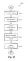
- FIG. 23is a flow illustrating a process 2300 for forming the package of some embodiments.
- the process 2300begins at the step 2310 , where a leadframe is provided.
- a leadframeis formed by etching and/or stamping a metal layer.
- the leadframeoptionally includes one or more contact terminals and/or one or more die attach pads.
- the process 2300transitions to the step 2320 , where a bonding means is coupled to the leadframe and/or to a semiconductor device. For instance, in some embodiments, solder balls are placed on a top surface of the leadframe and/or on a surface of the semiconductor device.
- couplingis achieved by screen printing the leadframe with solder on its surface at a location of solder balls or pillar bumps.
- the solder balls or pillar bumpsare attached to the circuit surface.
- the process 2300transitions to the step 2330 , where the semiconductor device is attached and/or bonded to the leadframe, including the contact terminals and/or attach pads of the leadframe.
- the bondingis performed by using conventional bonding means including, but not limited to, solder, solder balls, and/or pillar bumps.
- bondingis effectuated by a standard semiconductor assembly reflow process.
- the process 2300transitions to the step 2340 , where a thermally conductive layer is formed.
- the thermally conductive layerincludes a thermally and electrically conductive cushion.
- the cushion of some embodimentsis formed by applying a layer of thermally conductive adhesive and/or epoxy to a surface of the semiconductor device.
- some embodimentsinclude an additional thermally conductive, electrically insulating cap structure.
- the epoxyis optionally applied to a surface of the cap structure.
- the cap structureis then coupled to the semiconductor device by via the layer of epoxy.
- the cap structurecomprises a material that has particular heat transference and electrical insulating properties, such as a ceramic, for example.
- the thermally and electrically conductive epoxyis replaced by solder paste.
- a copper layeris applied to the solder paste, and the cap structure is applied to the copper layer.
- a high temperature eutectic melting processis formed to join the copper layer to the cap structure.
- the cap structureforms the top surface, or a portion thereof, of the package.
- a second copper layeris applied to the top surface of the cap structure such that the cap structure is sandwiched between the two copper layers. The two copper layers are applied prior to the high temperature eutectic melting process.
- a heat sinkis applied to the top of the package such that the heat sink is thermally coupled to the second copper layer.
- the heat sinkis coupled to the second copper layer using a thermally conductive adhesive or solder.
- the process 2300transitions to the step 2350 , where a molding compound is used to encapsulate the package.
- the encapsulation at the step 2350leaves a bottom surface of the contact terminal(s) and/or attach pad(s) exposed at the exterior of the package.
- the encapsulationleaves a top surface of the thermally conductive layer, such as the thermally conductive cushion, the cap structure, the electrical insulating material, or the copper layer, exposed at an exterior of the package.
- the step 2350 of some embodimentsalternatively includes additional steps such as singulation, etching, and/or stamping or other means to leave the selected thermally and/or electrically conductive elements of the package exposed at the exterior surfaces.
Landscapes
- Physics & Mathematics (AREA)
- Condensed Matter Physics & Semiconductors (AREA)
- General Physics & Mathematics (AREA)
- Engineering & Computer Science (AREA)
- Computer Hardware Design (AREA)
- Microelectronics & Electronic Packaging (AREA)
- Power Engineering (AREA)
- Cooling Or The Like Of Semiconductors Or Solid State Devices (AREA)
Abstract
Description
Claims (21)
Priority Applications (1)
| Application Number | Priority Date | Filing Date | Title |
|---|---|---|---|
| US12/868,560US8125077B2 (en) | 2006-09-26 | 2010-08-25 | Package with heat transfer |
Applications Claiming Priority (4)
| Application Number | Priority Date | Filing Date | Title |
|---|---|---|---|
| US84743406P | 2006-09-26 | 2006-09-26 | |
| US11/899,189US8013437B1 (en) | 2006-09-26 | 2007-09-04 | Package with heat transfer |
| US34905610P | 2010-05-27 | 2010-05-27 | |
| US12/868,560US8125077B2 (en) | 2006-09-26 | 2010-08-25 | Package with heat transfer |
Related Parent Applications (1)
| Application Number | Title | Priority Date | Filing Date |
|---|---|---|---|
| US11/899,189Continuation-In-PartUS8013437B1 (en) | 2006-09-26 | 2007-09-04 | Package with heat transfer |
Publications (2)
| Publication Number | Publication Date |
|---|---|
| US20100327432A1 US20100327432A1 (en) | 2010-12-30 |
| US8125077B2true US8125077B2 (en) | 2012-02-28 |
Family
ID=43379785
Family Applications (1)
| Application Number | Title | Priority Date | Filing Date |
|---|---|---|---|
| US12/868,560ActiveUS8125077B2 (en) | 2006-09-26 | 2010-08-25 | Package with heat transfer |
Country Status (1)
| Country | Link |
|---|---|
| US (1) | US8125077B2 (en) |
Cited By (2)
| Publication number | Priority date | Publication date | Assignee | Title |
|---|---|---|---|---|
| US20120001315A1 (en)* | 2010-06-30 | 2012-01-05 | Hitachi, Ltd. | Semiconductor device |
| US11195774B2 (en) | 2019-08-23 | 2021-12-07 | Samsung Electronics Co., Ltd. | Semiconductor packages |
Families Citing this family (15)
| Publication number | Priority date | Publication date | Assignee | Title |
|---|---|---|---|---|
| US8013437B1 (en) | 2006-09-26 | 2011-09-06 | Utac Thai Limited | Package with heat transfer |
| US9761435B1 (en) | 2006-12-14 | 2017-09-12 | Utac Thai Limited | Flip chip cavity package |
| US9947605B2 (en) | 2008-09-04 | 2018-04-17 | UTAC Headquarters Pte. Ltd. | Flip chip cavity package |
| JP2012230981A (en)* | 2011-04-26 | 2012-11-22 | Elpida Memory Inc | Semiconductor device and manufacturing method of the same |
| US9559064B2 (en)* | 2013-12-04 | 2017-01-31 | Taiwan Semiconductor Manufacturing Company, Ltd. | Warpage control in package-on-package structures |
| US9509251B2 (en) | 2015-03-24 | 2016-11-29 | Freescale Semiconductor, Inc. | RF amplifier module and methods of manufacture thereof |
| US10075132B2 (en) | 2015-03-24 | 2018-09-11 | Nxp Usa, Inc. | RF amplifier with conductor-less region underlying filter circuit inductor, and methods of manufacture thereof |
| US9871107B2 (en) | 2015-05-22 | 2018-01-16 | Nxp Usa, Inc. | Device with a conductive feature formed over a cavity and method therefor |
| US9787254B2 (en)* | 2015-09-23 | 2017-10-10 | Nxp Usa, Inc. | Encapsulated semiconductor device package with heatsink opening, and methods of manufacture thereof |
| US9917038B1 (en) | 2015-11-10 | 2018-03-13 | Utac Headquarters Pte Ltd | Semiconductor package with multiple molding routing layers and a method of manufacturing the same |
| US10276477B1 (en) | 2016-05-20 | 2019-04-30 | UTAC Headquarters Pte. Ltd. | Semiconductor package with multiple stacked leadframes and a method of manufacturing the same |
| US10319666B2 (en)* | 2017-04-19 | 2019-06-11 | International Business Machines Corporation | Thermal interface material structures including protruding surface features to reduce thermal interface material migration |
| US11107747B2 (en)* | 2018-09-19 | 2021-08-31 | Taiwan Semiconductor Manufacturing Co., Ltd. | Semiconductor package with composite thermal interface material structure and method of forming the same |
| JPWO2023153334A1 (en)* | 2022-02-14 | 2023-08-17 | ||
| US12211759B2 (en)* | 2022-02-22 | 2025-01-28 | Nxp Usa, Inc. | Circuit die with isolation test structure |
Citations (108)
| Publication number | Priority date | Publication date | Assignee | Title |
|---|---|---|---|---|
| US3611061A (en) | 1971-07-07 | 1971-10-05 | Motorola Inc | Multiple lead integrated circuit device and frame member for the fabrication thereof |
| US4411719A (en) | 1980-02-07 | 1983-10-25 | Westinghouse Electric Corp. | Apparatus and method for tape bonding and testing of integrated circuit chips |
| US4501960A (en) | 1981-06-22 | 1985-02-26 | Motorola, Inc. | Micropackage for identification card |
| US4801561A (en) | 1984-07-05 | 1989-01-31 | National Semiconductor Corporation | Method for making a pre-testable semiconductor die package |
| US4855672A (en) | 1987-05-18 | 1989-08-08 | Shreeve Robert W | Method and process for testing the reliability of integrated circuit (IC) chips and novel IC circuitry for accomplishing same |
| US5247248A (en) | 1991-02-18 | 1993-09-21 | Sharp Kabushiki Kaisha | Burn-in apparatus and method of use thereof |
| US5248075A (en) | 1992-04-13 | 1993-09-28 | Micron Technology, Inc. | IC pin forming machine with integrated IC testing capability |
| US5396185A (en) | 1990-08-13 | 1995-03-07 | Kabushiki Kaisha Toshiba | System and carrier for testing semiconductor integrated circuit devices |
| US5397921A (en) | 1993-09-03 | 1995-03-14 | Advanced Semiconductor Assembly Technology | Tab grid array |
| US5479105A (en) | 1993-06-25 | 1995-12-26 | Samsung Electronics Co., Ltd. | Known-good die testing apparatus |
| US5535101A (en) | 1992-11-03 | 1996-07-09 | Motorola, Inc. | Leadless integrated circuit package |
| US5596231A (en) | 1991-08-05 | 1997-01-21 | Asat, Limited | High power dissipation plastic encapsulated package for integrated circuit die |
| US5843808A (en) | 1996-01-11 | 1998-12-01 | Asat, Limited | Structure and method for automated assembly of a tab grid array package |
| US5990692A (en) | 1996-05-10 | 1999-11-23 | Samsung Electronics Co., Ltd. | Testing apparatus for non-packaged semiconductor chip |
| US6072239A (en) | 1995-11-08 | 2000-06-06 | Fujitsu Limited | Device having resin package with projections |
| US6111324A (en) | 1998-02-05 | 2000-08-29 | Asat, Limited | Integrated carrier ring/stiffener and method for manufacturing a flexible integrated circuit package |
| US6159770A (en) | 1995-11-08 | 2000-12-12 | Fujitsu Limited | Method and apparatus for fabricating semiconductor device |
| US6229200B1 (en) | 1998-06-10 | 2001-05-08 | Asat Limited | Saw-singulated leadless plastic chip carrier |
| US6285075B1 (en) | 1998-11-02 | 2001-09-04 | Asat, Limited | Integrated circuit package with bonding planes on a ceramic ring using an adhesive assembly |
| US6294100B1 (en) | 1998-06-10 | 2001-09-25 | Asat Ltd | Exposed die leadless plastic chip carrier |
| US6304000B1 (en) | 1997-04-30 | 2001-10-16 | Dow Corning Toray Silicone Company, Ltd. | Semiconductor device comprising silicone adhesive sheet |
| US6326678B1 (en) | 1993-09-03 | 2001-12-04 | Asat, Limited | Molded plastic package with heat sink and enhanced electrical performance |
| US6329711B1 (en) | 1995-11-08 | 2001-12-11 | Fujitsu Limited | Semiconductor device and mounting structure |
| US6353263B1 (en) | 1999-04-14 | 2002-03-05 | Sharp Kabushiki Kaisha | Semiconductor device and manufacturing method thereof |
| US6376921B1 (en) | 1995-11-08 | 2002-04-23 | Fujitsu Limited | Semiconductor device, method for fabricating the semiconductor device, lead frame and method for producing the lead frame |
| US6392427B1 (en) | 1998-12-21 | 2002-05-21 | Kaitech Engineering, Inc. | Testing electronic devices |
| US6414385B1 (en)* | 1999-11-08 | 2002-07-02 | Siliconware Precisionindustries Co., Ltd. | Quad flat non-lead package of semiconductor |
| US6429048B1 (en) | 2000-12-05 | 2002-08-06 | Asat Ltd. | Metal foil laminated IC package |
| US20020109214A1 (en) | 2001-02-14 | 2002-08-15 | Masanori Minamio | Leadframe, resin-molded semiconductor device including the leadframe, method of making the leadframe and method for manufacturing the device |
| US6451709B1 (en)* | 1998-09-03 | 2002-09-17 | Micron Technology, Inc. | Methodology of removing misplaced encapsulant for attachment of heat sinks in a chip on board package |
| US6455348B1 (en) | 1998-03-12 | 2002-09-24 | Matsushita Electric Industrial Co., Ltd. | Lead frame, resin-molded semiconductor device, and method for manufacturing the same |
| US6489218B1 (en) | 2001-06-21 | 2002-12-03 | Advanced Semiconductor Engineering, Inc. | Singulation method used in leadless packaging process |
| US6498099B1 (en) | 1998-06-10 | 2002-12-24 | Asat Ltd. | Leadless plastic chip carrier with etch back pad singulation |
| US20030006055A1 (en) | 2001-07-05 | 2003-01-09 | Walsin Advanced Electronics Ltd | Semiconductor package for fixed surface mounting |
| US6507116B1 (en) | 1997-04-24 | 2003-01-14 | International Business Machines Corporation | Electronic package and method of forming |
| US20030045032A1 (en) | 2001-08-31 | 2003-03-06 | Shinko Electric Industries Co., Ltd. | Leadframe, method of manufacturing the same, semiconductor device using the same, and method of manufacturing the device |
| US6545347B2 (en) | 2001-03-06 | 2003-04-08 | Asat, Limited | Enhanced leadless chip carrier |
| US6545332B2 (en) | 2001-01-17 | 2003-04-08 | Siliconware Precision Industries Co., Ltd. | Image sensor of a quad flat package |
| US20030071333A1 (en) | 2001-10-15 | 2003-04-17 | Shinko Electric Industries Co., Ltd. | Leadframe, method of manufacturing the same, and method of manufacturing a semiconductor device using the same |
| US6552417B2 (en) | 1993-09-03 | 2003-04-22 | Asat, Limited | Molded plastic package with heat sink and enhanced electrical performance |
| US6552423B2 (en) | 2000-02-18 | 2003-04-22 | Samsung Electronics Co., Ltd. | Higher-density memory card |
| US6566740B2 (en) | 2000-03-23 | 2003-05-20 | Mitsui High-Tec, Inc. | Lead frame for a semiconductor device and method of manufacturing a semiconductor device |
| US6586834B1 (en) | 2002-06-17 | 2003-07-01 | Asat Ltd. | Die-up tape ball grid array package |
| US6585905B1 (en) | 1998-06-10 | 2003-07-01 | Asat Ltd. | Leadless plastic chip carrier with partial etch die attach pad |
| US20030143776A1 (en) | 2002-01-31 | 2003-07-31 | Serafin Pedron | Method of manufacturing an encapsulated integrated circuit package |
| US20030178719A1 (en) | 2002-03-22 | 2003-09-25 | Combs Edward G. | Enhanced thermal dissipation integrated circuit package and method of manufacturing enhanced thermal dissipation integrated circuit package |
| US6635957B2 (en) | 1998-06-10 | 2003-10-21 | Asat Ltd. | Leadless plastic chip carrier with etch back pad singulation and die attach pad array |
| US20030201520A1 (en) | 2002-04-26 | 2003-10-30 | Knapp James H. | Structure and method of forming a multiple leadframe semiconductor device |
| US20030207498A1 (en) | 2002-04-29 | 2003-11-06 | Shafidul Islam | Partially patterned lead frames and methods of making and using the same in semiconductor packaging |
| US6667191B1 (en) | 2002-08-05 | 2003-12-23 | Asat Ltd. | Chip scale integrated circuit package |
| US20040014257A1 (en) | 2002-07-19 | 2004-01-22 | Kim Pyoung Wan | Method for joining lead frames in a package assembly, method for forming a chip stack package, and a chip stack package |
| US6686667B2 (en) | 2002-04-22 | 2004-02-03 | Scientek Corp. | Image sensor semiconductor package with castellation |
| US6703696B2 (en) | 2000-09-04 | 2004-03-09 | Dainippon Printing Co., Ltd. | Semiconductor package |
| US20040046237A1 (en) | 2002-09-05 | 2004-03-11 | Shinko Electric Industries Co., Ltd | Lead frame and method of manufacturing the same |
| US20040070055A1 (en) | 2002-02-26 | 2004-04-15 | St Assembly Test Services Pte Ltd | Ground plane for exposed package |
| US20040080025A1 (en) | 2002-09-17 | 2004-04-29 | Shinko Electric Industries Co., Ltd. | Lead frame, method of manufacturing the same, and semiconductor device manufactured with the same |
| US6734044B1 (en) | 2002-06-10 | 2004-05-11 | Asat Ltd. | Multiple leadframe laminated IC package |
| US6734552B2 (en)* | 2001-07-11 | 2004-05-11 | Asat Limited | Enhanced thermal dissipation integrated circuit package |
| US6737755B1 (en) | 2002-07-19 | 2004-05-18 | Asat, Ltd. | Ball grid array package with improved thermal characteristics |
| US20040110319A1 (en) | 1994-03-18 | 2004-06-10 | Hitachi Chemical Company, Ltd. | Fabrication process of semiconductor package and semiconductor package |
| US6764880B2 (en)* | 2001-11-15 | 2004-07-20 | Siliconware Precision Industries Co., Ltd. | Semiconductor package and fabricating method thereof |
| US6781242B1 (en) | 2002-12-02 | 2004-08-24 | Asat, Ltd. | Thin ball grid array package |
| US6812552B2 (en) | 2002-04-29 | 2004-11-02 | Advanced Interconnect Technologies Limited | Partially patterned lead frames and methods of making and using the same in semiconductor packaging |
| US6818980B1 (en) | 2003-05-07 | 2004-11-16 | Asat Ltd. | Stacked semiconductor package and method of manufacturing the same |
| US6818978B1 (en) | 2002-11-19 | 2004-11-16 | Asat Ltd. | Ball grid array package with shielding |
| US20050003586A1 (en) | 2001-05-11 | 2005-01-06 | Renesas Technology Corporation | Manufacturing method of a semiconductor device |
| US6841859B1 (en) | 2002-09-03 | 2005-01-11 | Asat Ltd. | Premolded cavity IC package |
| US6876066B2 (en) | 2001-08-29 | 2005-04-05 | Micron Technology, Inc. | Packaged microelectronic devices and methods of forming same |
| US20050077613A1 (en) | 2002-01-31 | 2005-04-14 | Mclellan Neil Robert | Integrated circuit package |
| US6897428B2 (en) | 2003-07-01 | 2005-05-24 | Matsushita Electric Industrial Co., Ltd. | Solid-state imaging device and method for manufacturing the same |
| US6933176B1 (en) | 2002-07-19 | 2005-08-23 | Asat Ltd. | Ball grid array package and process for manufacturing same |
| US6933594B2 (en) | 1998-06-10 | 2005-08-23 | Asat Ltd. | Leadless plastic chip carrier with etch back pad singulation |
| US6940154B2 (en) | 2002-06-24 | 2005-09-06 | Asat Limited | Integrated circuit package and method of manufacturing the integrated circuit package |
| US6946324B1 (en) | 1998-06-10 | 2005-09-20 | Asat Ltd. | Process for fabricating a leadless plastic chip carrier |
| US20050236701A1 (en) | 2002-10-24 | 2005-10-27 | Matsushita Electric Industrial Co., Ltd. | Leadframe, plastic-encapsulated semiconductor device, and method for fabricating the same |
| US6967126B2 (en) | 2001-07-31 | 2005-11-22 | Chippac, Inc. | Method for manufacturing plastic ball grid array with integral heatsink |
| US6979594B1 (en) | 2002-07-19 | 2005-12-27 | Asat Ltd. | Process for manufacturing ball grid array package |
| US6982491B1 (en) | 2004-01-20 | 2006-01-03 | Asat Ltd. | Sensor semiconductor package and method of manufacturing the same |
| US6984785B1 (en) | 2003-10-27 | 2006-01-10 | Asat Ltd. | Thermally enhanced cavity-down integrated circuit package |
| US7008825B1 (en) | 2003-05-27 | 2006-03-07 | Amkor Technology, Inc. | Leadframe strip having enhanced testability |
| US7009286B1 (en) | 2004-01-15 | 2006-03-07 | Asat Ltd. | Thin leadless plastic chip carrier |
| US20060071351A1 (en) | 2004-09-28 | 2006-04-06 | Texas Instruments Incorporated | Mold compound interlocking feature to improve semiconductor package strength |
| US7049177B1 (en) | 2004-01-28 | 2006-05-23 | Asat Ltd. | Leadless plastic chip carrier with standoff contacts and die attach pad |
| US7060535B1 (en) | 2003-10-29 | 2006-06-13 | Ns Electronics Bangkok (1993) Ltd. | Flat no-lead semiconductor die package including stud terminals |
| US7071545B1 (en) | 2002-12-20 | 2006-07-04 | Asat Ltd. | Shielded integrated circuit package |
| US7091581B1 (en) | 2004-06-14 | 2006-08-15 | Asat Limited | Integrated circuit package and process for fabricating the same |
| US20060192295A1 (en) | 2004-11-17 | 2006-08-31 | Chippac, Inc. | Semiconductor package flip chip interconnect having spacer |
| US7102210B2 (en) | 2003-09-05 | 2006-09-05 | Oki Electric Industry Co., Ltd. | Lead frame, manufacturing method of the same, and semiconductor device using the same |
| US7101210B2 (en) | 2004-11-26 | 2006-09-05 | Hon Hai Precision Ind. Co., Ltd. | LGA socket |
| US20060223237A1 (en) | 2001-07-11 | 2006-10-05 | Combs Edward G | Method of manufacturing enhanced thermal dissipation integrated circuit package |
| US20060273433A1 (en) | 2002-04-01 | 2006-12-07 | Matsushita Electric Industrial Co., Ltd. | Semiconductor device |
| US20070001278A1 (en) | 2005-06-30 | 2007-01-04 | Oseob Jeon | Semiconductor die package and method for making the same |
| US7205178B2 (en) | 2004-03-24 | 2007-04-17 | Freescale Semiconductor, Inc. | Land grid array packaged device and method of forming same |
| US7247526B1 (en) | 1998-06-10 | 2007-07-24 | Asat Ltd. | Process for fabricating an integrated circuit package |
| US20070200210A1 (en) | 2006-02-28 | 2007-08-30 | Broadcom Corporation | Methods and apparatus for improved thermal performance and electromagnetic interference (EMI) shielding in integrated circuit (IC) packages |
| US7274088B2 (en) | 2002-06-14 | 2007-09-25 | Siliconware Precision Industries Co., Ltd. | Flip-chip semiconductor package with lead frame as chip carrier and fabrication method thereof |
| US20070235217A1 (en) | 2006-03-29 | 2007-10-11 | Workman Derek B | Devices with microjetted polymer standoffs |
| US7314820B2 (en) | 2004-12-02 | 2008-01-01 | Siliconware Precision Industries Co., Ltd. | Carrier-free semiconductor package and fabrication method thereof |
| US20080048308A1 (en) | 2006-08-28 | 2008-02-28 | Atmel Corporation | Stackable packages for three-dimensional packaging of semiconductor dice |
| US7344920B1 (en) | 2005-07-15 | 2008-03-18 | Asat Ltd. | Integrated circuit package and method for fabricating same |
| US7358119B2 (en) | 2005-01-12 | 2008-04-15 | Asat Ltd. | Thin array plastic package without die attach pad and process for fabricating the same |
| US7372151B1 (en) | 2003-09-12 | 2008-05-13 | Asat Ltd. | Ball grid array package and process for manufacturing same |
| US20080150094A1 (en) | 2006-12-21 | 2008-06-26 | M/A-Com, Inc. | Flip chip shielded RF I/O land grid array package |
| US7399658B2 (en) | 2005-10-21 | 2008-07-15 | Stats Chippac Ltd. | Pre-molded leadframe and method therefor |
| US7408251B2 (en) | 2003-07-31 | 2008-08-05 | Renesas Technology Corp. | Semiconductor packaging device comprising a semiconductor chip including a MOSFET |
| US7411289B1 (en) | 2004-06-14 | 2008-08-12 | Asat Ltd. | Integrated circuit package with partially exposed contact pads and process for fabricating the same |
| US7595225B1 (en) | 2004-10-05 | 2009-09-29 | Chun Ho Fan | Leadless plastic chip carrier with contact standoff |
| US7714418B2 (en) | 2007-07-23 | 2010-05-11 | National Semiconductor Corporation | Leadframe panel |
- 2010
- 2010-08-25USUS12/868,560patent/US8125077B2/enactiveActive
Patent Citations (126)
| Publication number | Priority date | Publication date | Assignee | Title |
|---|---|---|---|---|
| US3611061A (en) | 1971-07-07 | 1971-10-05 | Motorola Inc | Multiple lead integrated circuit device and frame member for the fabrication thereof |
| US4411719A (en) | 1980-02-07 | 1983-10-25 | Westinghouse Electric Corp. | Apparatus and method for tape bonding and testing of integrated circuit chips |
| US4501960A (en) | 1981-06-22 | 1985-02-26 | Motorola, Inc. | Micropackage for identification card |
| US4801561A (en) | 1984-07-05 | 1989-01-31 | National Semiconductor Corporation | Method for making a pre-testable semiconductor die package |
| US4855672A (en) | 1987-05-18 | 1989-08-08 | Shreeve Robert W | Method and process for testing the reliability of integrated circuit (IC) chips and novel IC circuitry for accomplishing same |
| US5396185A (en) | 1990-08-13 | 1995-03-07 | Kabushiki Kaisha Toshiba | System and carrier for testing semiconductor integrated circuit devices |
| US5247248A (en) | 1991-02-18 | 1993-09-21 | Sharp Kabushiki Kaisha | Burn-in apparatus and method of use thereof |
| US5596231A (en) | 1991-08-05 | 1997-01-21 | Asat, Limited | High power dissipation plastic encapsulated package for integrated circuit die |
| US5248075A (en) | 1992-04-13 | 1993-09-28 | Micron Technology, Inc. | IC pin forming machine with integrated IC testing capability |
| US5535101A (en) | 1992-11-03 | 1996-07-09 | Motorola, Inc. | Leadless integrated circuit package |
| US5479105A (en) | 1993-06-25 | 1995-12-26 | Samsung Electronics Co., Ltd. | Known-good die testing apparatus |
| US6724071B2 (en) | 1993-09-03 | 2004-04-20 | Asat, Limited | Molded plastic package with heat sink and enhanced electrical performance |
| US6326678B1 (en) | 1993-09-03 | 2001-12-04 | Asat, Limited | Molded plastic package with heat sink and enhanced electrical performance |
| US6552417B2 (en) | 1993-09-03 | 2003-04-22 | Asat, Limited | Molded plastic package with heat sink and enhanced electrical performance |
| US5397921A (en) | 1993-09-03 | 1995-03-14 | Advanced Semiconductor Assembly Technology | Tab grid array |
| US20040110319A1 (en) | 1994-03-18 | 2004-06-10 | Hitachi Chemical Company, Ltd. | Fabrication process of semiconductor package and semiconductor package |
| US6329711B1 (en) | 1995-11-08 | 2001-12-11 | Fujitsu Limited | Semiconductor device and mounting structure |
| US6072239A (en) | 1995-11-08 | 2000-06-06 | Fujitsu Limited | Device having resin package with projections |
| US6573121B2 (en) | 1995-11-08 | 2003-06-03 | Fujitsu Limited | Semiconductor device, method for fabricating the semiconductor device, lead frame and method for producing the lead frame |
| US6159770A (en) | 1995-11-08 | 2000-12-12 | Fujitsu Limited | Method and apparatus for fabricating semiconductor device |
| US6376921B1 (en) | 1995-11-08 | 2002-04-23 | Fujitsu Limited | Semiconductor device, method for fabricating the semiconductor device, lead frame and method for producing the lead frame |
| US5843808A (en) | 1996-01-11 | 1998-12-01 | Asat, Limited | Structure and method for automated assembly of a tab grid array package |
| US5990692A (en) | 1996-05-10 | 1999-11-23 | Samsung Electronics Co., Ltd. | Testing apparatus for non-packaged semiconductor chip |
| US6507116B1 (en) | 1997-04-24 | 2003-01-14 | International Business Machines Corporation | Electronic package and method of forming |
| US6304000B1 (en) | 1997-04-30 | 2001-10-16 | Dow Corning Toray Silicone Company, Ltd. | Semiconductor device comprising silicone adhesive sheet |
| US6284569B1 (en) | 1998-02-05 | 2001-09-04 | Asat, Limited | Method of manufacturing a flexible integrated circuit package utilizing an integrated carrier ring/stiffener |
| US6111324A (en) | 1998-02-05 | 2000-08-29 | Asat, Limited | Integrated carrier ring/stiffener and method for manufacturing a flexible integrated circuit package |
| US6455348B1 (en) | 1998-03-12 | 2002-09-24 | Matsushita Electric Industrial Co., Ltd. | Lead frame, resin-molded semiconductor device, and method for manufacturing the same |
| US6946324B1 (en) | 1998-06-10 | 2005-09-20 | Asat Ltd. | Process for fabricating a leadless plastic chip carrier |
| US7482690B1 (en) | 1998-06-10 | 2009-01-27 | Asat Ltd. | Electronic components such as thin array plastic packages and process for fabricating same |
| US6294100B1 (en) | 1998-06-10 | 2001-09-25 | Asat Ltd | Exposed die leadless plastic chip carrier |
| US6995460B1 (en) | 1998-06-10 | 2006-02-07 | Asat Ltd. | Leadless plastic chip carrier with etch back pad singulation |
| US6585905B1 (en) | 1998-06-10 | 2003-07-01 | Asat Ltd. | Leadless plastic chip carrier with partial etch die attach pad |
| US6933594B2 (en) | 1998-06-10 | 2005-08-23 | Asat Ltd. | Leadless plastic chip carrier with etch back pad singulation |
| US6498099B1 (en) | 1998-06-10 | 2002-12-24 | Asat Ltd. | Leadless plastic chip carrier with etch back pad singulation |
| US6989294B1 (en) | 1998-06-10 | 2006-01-24 | Asat, Ltd. | Leadless plastic chip carrier with etch back pad singulation |
| US6242281B1 (en) | 1998-06-10 | 2001-06-05 | Asat, Limited | Saw-singulated leadless plastic chip carrier |
| US6229200B1 (en) | 1998-06-10 | 2001-05-08 | Asat Limited | Saw-singulated leadless plastic chip carrier |
| US6635957B2 (en) | 1998-06-10 | 2003-10-21 | Asat Ltd. | Leadless plastic chip carrier with etch back pad singulation and die attach pad array |
| US6964918B1 (en) | 1998-06-10 | 2005-11-15 | Asat Ltd. | Electronic components such as thin array plastic packages and process for fabricating same |
| US7247526B1 (en) | 1998-06-10 | 2007-07-24 | Asat Ltd. | Process for fabricating an integrated circuit package |
| US6451709B1 (en)* | 1998-09-03 | 2002-09-17 | Micron Technology, Inc. | Methodology of removing misplaced encapsulant for attachment of heat sinks in a chip on board package |
| US6285075B1 (en) | 1998-11-02 | 2001-09-04 | Asat, Limited | Integrated circuit package with bonding planes on a ceramic ring using an adhesive assembly |
| US6392427B1 (en) | 1998-12-21 | 2002-05-21 | Kaitech Engineering, Inc. | Testing electronic devices |
| US6353263B1 (en) | 1999-04-14 | 2002-03-05 | Sharp Kabushiki Kaisha | Semiconductor device and manufacturing method thereof |
| US6414385B1 (en)* | 1999-11-08 | 2002-07-02 | Siliconware Precisionindustries Co., Ltd. | Quad flat non-lead package of semiconductor |
| US6552423B2 (en) | 2000-02-18 | 2003-04-22 | Samsung Electronics Co., Ltd. | Higher-density memory card |
| US6566740B2 (en) | 2000-03-23 | 2003-05-20 | Mitsui High-Tec, Inc. | Lead frame for a semiconductor device and method of manufacturing a semiconductor device |
| US6703696B2 (en) | 2000-09-04 | 2004-03-09 | Dainippon Printing Co., Ltd. | Semiconductor package |
| US6429048B1 (en) | 2000-12-05 | 2002-08-06 | Asat Ltd. | Metal foil laminated IC package |
| US6545332B2 (en) | 2001-01-17 | 2003-04-08 | Siliconware Precision Industries Co., Ltd. | Image sensor of a quad flat package |
| US20020109214A1 (en) | 2001-02-14 | 2002-08-15 | Masanori Minamio | Leadframe, resin-molded semiconductor device including the leadframe, method of making the leadframe and method for manufacturing the device |
| US6545347B2 (en) | 2001-03-06 | 2003-04-08 | Asat, Limited | Enhanced leadless chip carrier |
| US20050003586A1 (en) | 2001-05-11 | 2005-01-06 | Renesas Technology Corporation | Manufacturing method of a semiconductor device |
| US6489218B1 (en) | 2001-06-21 | 2002-12-03 | Advanced Semiconductor Engineering, Inc. | Singulation method used in leadless packaging process |
| US20030006055A1 (en) | 2001-07-05 | 2003-01-09 | Walsin Advanced Electronics Ltd | Semiconductor package for fixed surface mounting |
| US6734552B2 (en)* | 2001-07-11 | 2004-05-11 | Asat Limited | Enhanced thermal dissipation integrated circuit package |
| US20060223237A1 (en) | 2001-07-11 | 2006-10-05 | Combs Edward G | Method of manufacturing enhanced thermal dissipation integrated circuit package |
| US6967126B2 (en) | 2001-07-31 | 2005-11-22 | Chippac, Inc. | Method for manufacturing plastic ball grid array with integral heatsink |
| US6876066B2 (en) | 2001-08-29 | 2005-04-05 | Micron Technology, Inc. | Packaged microelectronic devices and methods of forming same |
| US20030045032A1 (en) | 2001-08-31 | 2003-03-06 | Shinko Electric Industries Co., Ltd. | Leadframe, method of manufacturing the same, semiconductor device using the same, and method of manufacturing the device |
| US20030071333A1 (en) | 2001-10-15 | 2003-04-17 | Shinko Electric Industries Co., Ltd. | Leadframe, method of manufacturing the same, and method of manufacturing a semiconductor device using the same |
| US6764880B2 (en)* | 2001-11-15 | 2004-07-20 | Siliconware Precision Industries Co., Ltd. | Semiconductor package and fabricating method thereof |
| US20030143776A1 (en) | 2002-01-31 | 2003-07-31 | Serafin Pedron | Method of manufacturing an encapsulated integrated circuit package |
| US20050077613A1 (en) | 2002-01-31 | 2005-04-14 | Mclellan Neil Robert | Integrated circuit package |
| US20040070055A1 (en) | 2002-02-26 | 2004-04-15 | St Assembly Test Services Pte Ltd | Ground plane for exposed package |
| US20030178719A1 (en) | 2002-03-22 | 2003-09-25 | Combs Edward G. | Enhanced thermal dissipation integrated circuit package and method of manufacturing enhanced thermal dissipation integrated circuit package |
| US20060273433A1 (en) | 2002-04-01 | 2006-12-07 | Matsushita Electric Industrial Co., Ltd. | Semiconductor device |
| US6686667B2 (en) | 2002-04-22 | 2004-02-03 | Scientek Corp. | Image sensor semiconductor package with castellation |
| US20030201520A1 (en) | 2002-04-26 | 2003-10-30 | Knapp James H. | Structure and method of forming a multiple leadframe semiconductor device |
| US6812552B2 (en) | 2002-04-29 | 2004-11-02 | Advanced Interconnect Technologies Limited | Partially patterned lead frames and methods of making and using the same in semiconductor packaging |
| US20030207498A1 (en) | 2002-04-29 | 2003-11-06 | Shafidul Islam | Partially patterned lead frames and methods of making and using the same in semiconductor packaging |
| US6734044B1 (en) | 2002-06-10 | 2004-05-11 | Asat Ltd. | Multiple leadframe laminated IC package |
| US7449771B1 (en) | 2002-06-10 | 2008-11-11 | Asat Ltd. | Multiple leadframe laminated IC package |
| US7274088B2 (en) | 2002-06-14 | 2007-09-25 | Siliconware Precision Industries Co., Ltd. | Flip-chip semiconductor package with lead frame as chip carrier and fabrication method thereof |
| US6586834B1 (en) | 2002-06-17 | 2003-07-01 | Asat Ltd. | Die-up tape ball grid array package |
| US6940154B2 (en) | 2002-06-24 | 2005-09-06 | Asat Limited | Integrated circuit package and method of manufacturing the integrated circuit package |
| US6800948B1 (en) | 2002-07-19 | 2004-10-05 | Asat Ltd. | Ball grid array package |
| US7371610B1 (en) | 2002-07-19 | 2008-05-13 | Asat Ltd. | Process for fabricating an integrated circuit package with reduced mold warping |
| US7315080B1 (en) | 2002-07-19 | 2008-01-01 | Asat Ltd. | Ball grid array package that includes a collapsible spacer for separating die adapter from a heat spreader |
| US20060223229A1 (en) | 2002-07-19 | 2006-10-05 | Asat Ltd. | Ball grid array package and process for manufacturing same |
| US6933176B1 (en) | 2002-07-19 | 2005-08-23 | Asat Ltd. | Ball grid array package and process for manufacturing same |
| US6737755B1 (en) | 2002-07-19 | 2004-05-18 | Asat, Ltd. | Ball grid array package with improved thermal characteristics |
| US6979594B1 (en) | 2002-07-19 | 2005-12-27 | Asat Ltd. | Process for manufacturing ball grid array package |
| US6818472B1 (en) | 2002-07-19 | 2004-11-16 | Asat Ltd. | Ball grid array package |
| US20040014257A1 (en) | 2002-07-19 | 2004-01-22 | Kim Pyoung Wan | Method for joining lead frames in a package assembly, method for forming a chip stack package, and a chip stack package |
| US6667191B1 (en) | 2002-08-05 | 2003-12-23 | Asat Ltd. | Chip scale integrated circuit package |
| US7224048B1 (en) | 2002-08-05 | 2007-05-29 | Asat Ltd. | Flip chip ball grid array package |
| US6841859B1 (en) | 2002-09-03 | 2005-01-11 | Asat Ltd. | Premolded cavity IC package |
| US20040046237A1 (en) | 2002-09-05 | 2004-03-11 | Shinko Electric Industries Co., Ltd | Lead frame and method of manufacturing the same |
| US20040080025A1 (en) | 2002-09-17 | 2004-04-29 | Shinko Electric Industries Co., Ltd. | Lead frame, method of manufacturing the same, and semiconductor device manufactured with the same |
| US20050236701A1 (en) | 2002-10-24 | 2005-10-27 | Matsushita Electric Industrial Co., Ltd. | Leadframe, plastic-encapsulated semiconductor device, and method for fabricating the same |
| US6818978B1 (en) | 2002-11-19 | 2004-11-16 | Asat Ltd. | Ball grid array package with shielding |
| US6781242B1 (en) | 2002-12-02 | 2004-08-24 | Asat, Ltd. | Thin ball grid array package |
| US7071545B1 (en) | 2002-12-20 | 2006-07-04 | Asat Ltd. | Shielded integrated circuit package |
| US7381588B1 (en) | 2002-12-20 | 2008-06-03 | Asat Ltd. | Shielded integrated circuit package |
| US6818980B1 (en) | 2003-05-07 | 2004-11-16 | Asat Ltd. | Stacked semiconductor package and method of manufacturing the same |
| US7008825B1 (en) | 2003-05-27 | 2006-03-07 | Amkor Technology, Inc. | Leadframe strip having enhanced testability |
| US6897428B2 (en) | 2003-07-01 | 2005-05-24 | Matsushita Electric Industrial Co., Ltd. | Solid-state imaging device and method for manufacturing the same |
| US7408251B2 (en) | 2003-07-31 | 2008-08-05 | Renesas Technology Corp. | Semiconductor packaging device comprising a semiconductor chip including a MOSFET |
| US7102210B2 (en) | 2003-09-05 | 2006-09-05 | Oki Electric Industry Co., Ltd. | Lead frame, manufacturing method of the same, and semiconductor device using the same |
| US7372151B1 (en) | 2003-09-12 | 2008-05-13 | Asat Ltd. | Ball grid array package and process for manufacturing same |
| US6984785B1 (en) | 2003-10-27 | 2006-01-10 | Asat Ltd. | Thermally enhanced cavity-down integrated circuit package |
| US7342305B1 (en) | 2003-10-27 | 2008-03-11 | Asat Ltd. | Thermally enhanced cavity-down integrated circuit package |
| US7060535B1 (en) | 2003-10-29 | 2006-06-13 | Ns Electronics Bangkok (1993) Ltd. | Flat no-lead semiconductor die package including stud terminals |
| US7009286B1 (en) | 2004-01-15 | 2006-03-07 | Asat Ltd. | Thin leadless plastic chip carrier |
| US6982491B1 (en) | 2004-01-20 | 2006-01-03 | Asat Ltd. | Sensor semiconductor package and method of manufacturing the same |
| US7049177B1 (en) | 2004-01-28 | 2006-05-23 | Asat Ltd. | Leadless plastic chip carrier with standoff contacts and die attach pad |
| US7205178B2 (en) | 2004-03-24 | 2007-04-17 | Freescale Semiconductor, Inc. | Land grid array packaged device and method of forming same |
| US7091581B1 (en) | 2004-06-14 | 2006-08-15 | Asat Limited | Integrated circuit package and process for fabricating the same |
| US7411289B1 (en) | 2004-06-14 | 2008-08-12 | Asat Ltd. | Integrated circuit package with partially exposed contact pads and process for fabricating the same |
| US20060071351A1 (en) | 2004-09-28 | 2006-04-06 | Texas Instruments Incorporated | Mold compound interlocking feature to improve semiconductor package strength |
| US7595225B1 (en) | 2004-10-05 | 2009-09-29 | Chun Ho Fan | Leadless plastic chip carrier with contact standoff |
| US20060192295A1 (en) | 2004-11-17 | 2006-08-31 | Chippac, Inc. | Semiconductor package flip chip interconnect having spacer |
| US7101210B2 (en) | 2004-11-26 | 2006-09-05 | Hon Hai Precision Ind. Co., Ltd. | LGA socket |
| US7314820B2 (en) | 2004-12-02 | 2008-01-01 | Siliconware Precision Industries Co., Ltd. | Carrier-free semiconductor package and fabrication method thereof |
| US7358119B2 (en) | 2005-01-12 | 2008-04-15 | Asat Ltd. | Thin array plastic package without die attach pad and process for fabricating the same |
| US20070001278A1 (en) | 2005-06-30 | 2007-01-04 | Oseob Jeon | Semiconductor die package and method for making the same |
| US7348663B1 (en) | 2005-07-15 | 2008-03-25 | Asat Ltd. | Integrated circuit package and method for fabricating same |
| US7344920B1 (en) | 2005-07-15 | 2008-03-18 | Asat Ltd. | Integrated circuit package and method for fabricating same |
| US7399658B2 (en) | 2005-10-21 | 2008-07-15 | Stats Chippac Ltd. | Pre-molded leadframe and method therefor |
| US20070200210A1 (en) | 2006-02-28 | 2007-08-30 | Broadcom Corporation | Methods and apparatus for improved thermal performance and electromagnetic interference (EMI) shielding in integrated circuit (IC) packages |
| US20070235217A1 (en) | 2006-03-29 | 2007-10-11 | Workman Derek B | Devices with microjetted polymer standoffs |
| US20080048308A1 (en) | 2006-08-28 | 2008-02-28 | Atmel Corporation | Stackable packages for three-dimensional packaging of semiconductor dice |
| US20080150094A1 (en) | 2006-12-21 | 2008-06-26 | M/A-Com, Inc. | Flip chip shielded RF I/O land grid array package |
| US7714418B2 (en) | 2007-07-23 | 2010-05-11 | National Semiconductor Corporation | Leadframe panel |
Non-Patent Citations (3)
| Title |
|---|
| Michael Quirk and Julian Serda, Semiconductor Manufacturing Technology, Pearson Education International, Pearson Prentice Hall, 2001, p. 587-588. |
| Notice of Allowance dated Jun. 17, 2011, U.S. Appl. No. 11/899,189, filed Sep. 4, 2007, Saravuth Sirinorakul et al. |
| Office Action dated Oct. 26, 2010, U.S. Appl. No. 11/899,189, filed Sep. 4, 2007, Saravuth Sirinorakul et al. |
Cited By (3)
| Publication number | Priority date | Publication date | Assignee | Title |
|---|---|---|---|---|
| US20120001315A1 (en)* | 2010-06-30 | 2012-01-05 | Hitachi, Ltd. | Semiconductor device |
| US8441115B2 (en)* | 2010-06-30 | 2013-05-14 | Hitachi, Ltd. | Semiconductor device with exposed thermal conductivity part |
| US11195774B2 (en) | 2019-08-23 | 2021-12-07 | Samsung Electronics Co., Ltd. | Semiconductor packages |
Also Published As
| Publication number | Publication date |
|---|---|
| US20100327432A1 (en) | 2010-12-30 |
Similar Documents
| Publication | Publication Date | Title |
|---|---|---|
| US8125077B2 (en) | Package with heat transfer | |
| US8564124B2 (en) | Semiconductor package | |
| US6507104B2 (en) | Semiconductor package with embedded heat-dissipating device | |
| US6404049B1 (en) | Semiconductor device, manufacturing method thereof and mounting board | |
| JP3150351B2 (en) | Electronic device and method of manufacturing the same | |
| KR100370231B1 (en) | Power module package having a insulator type heat sink attached a backside of leadframe & manufacturing method thereof | |
| US6882041B1 (en) | Thermally enhanced metal capped BGA package | |
| EP1256980B1 (en) | Ball grid array package with a heat spreader and method for making the same | |
| US6429513B1 (en) | Active heat sink for cooling a semiconductor chip | |
| KR100632459B1 (en) | Heat-dissipating semiconductor package and manufacturing method | |
| US20030011054A1 (en) | Power module package having improved heat dissipating capability | |
| US7312525B2 (en) | Thermally enhanced package for an integrated circuit | |
| US11862542B2 (en) | Dual side cooling power module and manufacturing method of the same | |
| US8013437B1 (en) | Package with heat transfer | |
| WO2022056679A1 (en) | Power module and manufacturing method therefor, converter, and electronic device | |
| WO2008082969A1 (en) | Thermally enhanced quad flat no leads (qfn) ic package and method | |
| US6627990B1 (en) | Thermally enhanced stacked die package | |
| US20100123243A1 (en) | Flip-chip chip-scale package structure | |
| US7361995B2 (en) | Molded high density electronic packaging structure for high performance applications | |
| JP5341339B2 (en) | Circuit equipment | |
| JP2007281201A (en) | Semiconductor device | |
| US20200203259A1 (en) | Integrated circuit package | |
| CN116759397A (en) | Chip packaging structure and preparation method thereof | |
| KR19990025039U (en) | Stacked Ball Grid Array Package |
Legal Events
| Date | Code | Title | Description |
|---|---|---|---|
| AS | Assignment | Owner name:UTAC THAI LIMITED, THAILAND Free format text:ASSIGNMENT OF ASSIGNORS INTEREST;ASSIGNORS:SIRINORAKUL, SARAVUTH;NONDHASITTHICHAI, SOMCHAI;REEL/FRAME:024887/0728 Effective date:20100823 | |
| STCF | Information on status: patent grant | Free format text:PATENTED CASE | |
| FEPP | Fee payment procedure | Free format text:PAYOR NUMBER ASSIGNED (ORIGINAL EVENT CODE: ASPN); ENTITY STATUS OF PATENT OWNER: LARGE ENTITY | |
| FPAY | Fee payment | Year of fee payment:4 | |
| AS | Assignment | Owner name:UTAC HEADQUARTERS PTE. LTD., SINGAPORE Free format text:ASSIGNMENT OF ASSIGNORS INTEREST;ASSIGNOR:UTAC THAI LIMITED;REEL/FRAME:037959/0937 Effective date:20150508 | |
| AS | Assignment | Owner name:UTAC HEADQUARTERS PTE. LTD., SINGAPORE Free format text:CORRECTIVE ASSIGNMENT TO ADD THE ANNEX A AND THE ANNEX B WHICH WAS INADVERTENTLY LEFTOUT IN THE ORIGINAL ASSIGNMENT DOCUMENT PREVIOUSLY RECORDED ON REEL 037959 FRAME 0937. ASSIGNOR(S) HEREBY CONFIRMS THE ASSIGNMENT;ASSIGNOR:UTAC THAI LIMITED;REEL/FRAME:039902/0302 Effective date:20150508 | |
| MAFP | Maintenance fee payment | Free format text:PAYMENT OF MAINTENANCE FEE, 8TH YEAR, LARGE ENTITY (ORIGINAL EVENT CODE: M1552); ENTITY STATUS OF PATENT OWNER: LARGE ENTITY Year of fee payment:8 | |
| MAFP | Maintenance fee payment | Free format text:PAYMENT OF MAINTENANCE FEE, 12TH YEAR, LARGE ENTITY (ORIGINAL EVENT CODE: M1553); ENTITY STATUS OF PATENT OWNER: LARGE ENTITY Year of fee payment:12 |