US8125064B1 - Increased I/O semiconductor package and method of making same - Google Patents
Increased I/O semiconductor package and method of making sameDownload PDFInfo
- Publication number
- US8125064B1 US8125064B1US12/181,256US18125608AUS8125064B1US 8125064 B1US8125064 B1US 8125064B1US 18125608 AUS18125608 AUS 18125608AUS 8125064 B1US8125064 B1US 8125064B1
- Authority
- US
- United States
- Prior art keywords
- substrate
- semiconductor package
- lands
- holes
- semiconductor die
- Prior art date
- Legal status (The legal status is an assumption and is not a legal conclusion. Google has not performed a legal analysis and makes no representation as to the accuracy of the status listed.)
- Active, expires
Links
- 239000004065semiconductorSubstances0.000titleclaimsabstractdescription206
- 238000004519manufacturing processMethods0.000titleabstractdescription23
- 239000000758substrateSubstances0.000claimsabstractdescription180
- 229910052751metalInorganic materials0.000claimsabstractdescription81
- 239000002184metalSubstances0.000claimsabstractdescription81
- 238000009413insulationMethods0.000claimsdescription60
- 229910000679solderInorganic materials0.000claimsdescription36
- 239000008393encapsulating agentSubstances0.000claimsdescription34
- 230000008878couplingEffects0.000claimsdescription15
- 238000010168coupling processMethods0.000claimsdescription15
- 238000005859coupling reactionMethods0.000claimsdescription15
- 230000002093peripheral effectEffects0.000claimsdescription13
- 230000035515penetrationEffects0.000claimsdescription9
- PXHVJJICTQNCMI-UHFFFAOYSA-NNickelChemical compound[Ni]PXHVJJICTQNCMI-UHFFFAOYSA-N0.000claimsdescription6
- 229910001092metal group alloyInorganic materials0.000claimsdescription5
- RYGMFSIKBFXOCR-UHFFFAOYSA-NCopperChemical compound[Cu]RYGMFSIKBFXOCR-UHFFFAOYSA-N0.000claimsdescription4
- 229910052782aluminiumInorganic materials0.000claimsdescription4
- XAGFODPZIPBFFR-UHFFFAOYSA-NaluminiumChemical compound[Al]XAGFODPZIPBFFR-UHFFFAOYSA-N0.000claimsdescription4
- 229910052802copperInorganic materials0.000claimsdescription4
- 239000010949copperSubstances0.000claimsdescription4
- 229920005989resinPolymers0.000claimsdescription4
- 239000011347resinSubstances0.000claimsdescription4
- 229910052759nickelInorganic materials0.000claimsdescription3
- 238000000034methodMethods0.000abstractdescription34
- 239000000853adhesiveSubstances0.000description18
- 230000001070adhesive effectEffects0.000description18
- 238000005538encapsulationMethods0.000description7
- 238000005530etchingMethods0.000description7
- 239000000463materialSubstances0.000description6
- 239000007769metal materialSubstances0.000description6
- 150000002739metalsChemical class0.000description5
- 230000000149penetrating effectEffects0.000description5
- BQCADISMDOOEFD-UHFFFAOYSA-NSilverChemical compound[Ag]BQCADISMDOOEFD-UHFFFAOYSA-N0.000description4
- 229910052709silverInorganic materials0.000description4
- 239000004332silverSubstances0.000description4
- 238000010408sweepingMethods0.000description4
- ATJFFYVFTNAWJD-UHFFFAOYSA-NTinChemical compound[Sn]ATJFFYVFTNAWJD-UHFFFAOYSA-N0.000description3
- 239000011248coating agentSubstances0.000description3
- 238000000576coating methodMethods0.000description3
- 239000003822epoxy resinSubstances0.000description3
- 239000012774insulation materialSubstances0.000description3
- 229920000647polyepoxidePolymers0.000description3
- 229920002050silicone resinPolymers0.000description3
- 239000004593EpoxySubstances0.000description2
- 239000004952PolyamideSubstances0.000description1
- 239000002390adhesive tapeSubstances0.000description1
- 229910045601alloyInorganic materials0.000description1
- 239000000956alloySubstances0.000description1
- 239000004020conductorSubstances0.000description1
- 230000003247decreasing effectEffects0.000description1
- 238000007598dipping methodMethods0.000description1
- 238000005553drillingMethods0.000description1
- 238000009713electroplatingMethods0.000description1
- PCHJSUWPFVWCPO-UHFFFAOYSA-NgoldChemical compound[Au]PCHJSUWPFVWCPO-UHFFFAOYSA-N0.000description1
- 229910052737goldInorganic materials0.000description1
- 239000010931goldSubstances0.000description1
- 238000000227grindingMethods0.000description1
- 239000012212insulatorSubstances0.000description1
- 230000000116mitigating effectEffects0.000description1
- 229920002647polyamidePolymers0.000description1
- 238000007639printingMethods0.000description1
- 238000007650screen-printingMethods0.000description1
- 238000000926separation methodMethods0.000description1
- 230000035939shockEffects0.000description1
- 239000007787solidSubstances0.000description1
- 238000005507sprayingMethods0.000description1
Images


Classifications
- H—ELECTRICITY
- H01—ELECTRIC ELEMENTS
- H01L—SEMICONDUCTOR DEVICES NOT COVERED BY CLASS H10
- H01L23/00—Details of semiconductor or other solid state devices
- H01L23/48—Arrangements for conducting electric current to or from the solid state body in operation, e.g. leads, terminal arrangements ; Selection of materials therefor
- H01L23/488—Arrangements for conducting electric current to or from the solid state body in operation, e.g. leads, terminal arrangements ; Selection of materials therefor consisting of soldered or bonded constructions
- H01L23/498—Leads, i.e. metallisations or lead-frames on insulating substrates, e.g. chip carriers
- H01L23/49838—Geometry or layout
- H—ELECTRICITY
- H01—ELECTRIC ELEMENTS
- H01L—SEMICONDUCTOR DEVICES NOT COVERED BY CLASS H10
- H01L23/00—Details of semiconductor or other solid state devices
- H01L23/12—Mountings, e.g. non-detachable insulating substrates
- H01L23/13—Mountings, e.g. non-detachable insulating substrates characterised by the shape
- H—ELECTRICITY
- H01—ELECTRIC ELEMENTS
- H01L—SEMICONDUCTOR DEVICES NOT COVERED BY CLASS H10
- H01L23/00—Details of semiconductor or other solid state devices
- H01L23/12—Mountings, e.g. non-detachable insulating substrates
- H01L23/14—Mountings, e.g. non-detachable insulating substrates characterised by the material or its electrical properties
- H01L23/142—Metallic substrates having insulating layers
- H—ELECTRICITY
- H01—ELECTRIC ELEMENTS
- H01L—SEMICONDUCTOR DEVICES NOT COVERED BY CLASS H10
- H01L23/00—Details of semiconductor or other solid state devices
- H01L23/28—Encapsulations, e.g. encapsulating layers, coatings, e.g. for protection
- H01L23/31—Encapsulations, e.g. encapsulating layers, coatings, e.g. for protection characterised by the arrangement or shape
- H01L23/3107—Encapsulations, e.g. encapsulating layers, coatings, e.g. for protection characterised by the arrangement or shape the device being completely enclosed
- H01L23/3142—Sealing arrangements between parts, e.g. adhesion promotors
- H—ELECTRICITY
- H01—ELECTRIC ELEMENTS
- H01L—SEMICONDUCTOR DEVICES NOT COVERED BY CLASS H10
- H01L23/00—Details of semiconductor or other solid state devices
- H01L23/48—Arrangements for conducting electric current to or from the solid state body in operation, e.g. leads, terminal arrangements ; Selection of materials therefor
- H01L23/488—Arrangements for conducting electric current to or from the solid state body in operation, e.g. leads, terminal arrangements ; Selection of materials therefor consisting of soldered or bonded constructions
- H01L23/498—Leads, i.e. metallisations or lead-frames on insulating substrates, e.g. chip carriers
- H01L23/49827—Via connections through the substrates, e.g. pins going through the substrate, coaxial cables
- H—ELECTRICITY
- H01—ELECTRIC ELEMENTS
- H01L—SEMICONDUCTOR DEVICES NOT COVERED BY CLASS H10
- H01L2224/00—Indexing scheme for arrangements for connecting or disconnecting semiconductor or solid-state bodies and methods related thereto as covered by H01L24/00
- H01L2224/01—Means for bonding being attached to, or being formed on, the surface to be connected, e.g. chip-to-package, die-attach, "first-level" interconnects; Manufacturing methods related thereto
- H01L2224/10—Bump connectors; Manufacturing methods related thereto
- H01L2224/15—Structure, shape, material or disposition of the bump connectors after the connecting process
- H01L2224/16—Structure, shape, material or disposition of the bump connectors after the connecting process of an individual bump connector
- H01L2224/161—Disposition
- H01L2224/16151—Disposition the bump connector connecting between a semiconductor or solid-state body and an item not being a semiconductor or solid-state body, e.g. chip-to-substrate, chip-to-passive
- H01L2224/16221—Disposition the bump connector connecting between a semiconductor or solid-state body and an item not being a semiconductor or solid-state body, e.g. chip-to-substrate, chip-to-passive the body and the item being stacked
- H01L2224/16225—Disposition the bump connector connecting between a semiconductor or solid-state body and an item not being a semiconductor or solid-state body, e.g. chip-to-substrate, chip-to-passive the body and the item being stacked the item being non-metallic, e.g. insulating substrate with or without metallisation
- H—ELECTRICITY
- H01—ELECTRIC ELEMENTS
- H01L—SEMICONDUCTOR DEVICES NOT COVERED BY CLASS H10
- H01L2224/00—Indexing scheme for arrangements for connecting or disconnecting semiconductor or solid-state bodies and methods related thereto as covered by H01L24/00
- H01L2224/01—Means for bonding being attached to, or being formed on, the surface to be connected, e.g. chip-to-package, die-attach, "first-level" interconnects; Manufacturing methods related thereto
- H01L2224/26—Layer connectors, e.g. plate connectors, solder or adhesive layers; Manufacturing methods related thereto
- H01L2224/31—Structure, shape, material or disposition of the layer connectors after the connecting process
- H01L2224/32—Structure, shape, material or disposition of the layer connectors after the connecting process of an individual layer connector
- H01L2224/321—Disposition
- H01L2224/32135—Disposition the layer connector connecting between different semiconductor or solid-state bodies, i.e. chip-to-chip
- H01L2224/32145—Disposition the layer connector connecting between different semiconductor or solid-state bodies, i.e. chip-to-chip the bodies being stacked
- H—ELECTRICITY
- H01—ELECTRIC ELEMENTS
- H01L—SEMICONDUCTOR DEVICES NOT COVERED BY CLASS H10
- H01L2224/00—Indexing scheme for arrangements for connecting or disconnecting semiconductor or solid-state bodies and methods related thereto as covered by H01L24/00
- H01L2224/01—Means for bonding being attached to, or being formed on, the surface to be connected, e.g. chip-to-package, die-attach, "first-level" interconnects; Manufacturing methods related thereto
- H01L2224/26—Layer connectors, e.g. plate connectors, solder or adhesive layers; Manufacturing methods related thereto
- H01L2224/31—Structure, shape, material or disposition of the layer connectors after the connecting process
- H01L2224/32—Structure, shape, material or disposition of the layer connectors after the connecting process of an individual layer connector
- H01L2224/321—Disposition
- H01L2224/32151—Disposition the layer connector connecting between a semiconductor or solid-state body and an item not being a semiconductor or solid-state body, e.g. chip-to-substrate, chip-to-passive
- H01L2224/32221—Disposition the layer connector connecting between a semiconductor or solid-state body and an item not being a semiconductor or solid-state body, e.g. chip-to-substrate, chip-to-passive the body and the item being stacked
- H01L2224/32225—Disposition the layer connector connecting between a semiconductor or solid-state body and an item not being a semiconductor or solid-state body, e.g. chip-to-substrate, chip-to-passive the body and the item being stacked the item being non-metallic, e.g. insulating substrate with or without metallisation
- H—ELECTRICITY
- H01—ELECTRIC ELEMENTS
- H01L—SEMICONDUCTOR DEVICES NOT COVERED BY CLASS H10
- H01L2224/00—Indexing scheme for arrangements for connecting or disconnecting semiconductor or solid-state bodies and methods related thereto as covered by H01L24/00
- H01L2224/01—Means for bonding being attached to, or being formed on, the surface to be connected, e.g. chip-to-package, die-attach, "first-level" interconnects; Manufacturing methods related thereto
- H01L2224/42—Wire connectors; Manufacturing methods related thereto
- H01L2224/47—Structure, shape, material or disposition of the wire connectors after the connecting process
- H01L2224/48—Structure, shape, material or disposition of the wire connectors after the connecting process of an individual wire connector
- H01L2224/4805—Shape
- H01L2224/4809—Loop shape
- H01L2224/48091—Arched
- H—ELECTRICITY
- H01—ELECTRIC ELEMENTS
- H01L—SEMICONDUCTOR DEVICES NOT COVERED BY CLASS H10
- H01L2224/00—Indexing scheme for arrangements for connecting or disconnecting semiconductor or solid-state bodies and methods related thereto as covered by H01L24/00
- H01L2224/01—Means for bonding being attached to, or being formed on, the surface to be connected, e.g. chip-to-package, die-attach, "first-level" interconnects; Manufacturing methods related thereto
- H01L2224/42—Wire connectors; Manufacturing methods related thereto
- H01L2224/47—Structure, shape, material or disposition of the wire connectors after the connecting process
- H01L2224/48—Structure, shape, material or disposition of the wire connectors after the connecting process of an individual wire connector
- H01L2224/481—Disposition
- H01L2224/48151—Connecting between a semiconductor or solid-state body and an item not being a semiconductor or solid-state body, e.g. chip-to-substrate, chip-to-passive
- H01L2224/48221—Connecting between a semiconductor or solid-state body and an item not being a semiconductor or solid-state body, e.g. chip-to-substrate, chip-to-passive the body and the item being stacked
- H01L2224/48225—Connecting between a semiconductor or solid-state body and an item not being a semiconductor or solid-state body, e.g. chip-to-substrate, chip-to-passive the body and the item being stacked the item being non-metallic, e.g. insulating substrate with or without metallisation
- H01L2224/48227—Connecting between a semiconductor or solid-state body and an item not being a semiconductor or solid-state body, e.g. chip-to-substrate, chip-to-passive the body and the item being stacked the item being non-metallic, e.g. insulating substrate with or without metallisation connecting the wire to a bond pad of the item
- H—ELECTRICITY
- H01—ELECTRIC ELEMENTS
- H01L—SEMICONDUCTOR DEVICES NOT COVERED BY CLASS H10
- H01L2224/00—Indexing scheme for arrangements for connecting or disconnecting semiconductor or solid-state bodies and methods related thereto as covered by H01L24/00
- H01L2224/01—Means for bonding being attached to, or being formed on, the surface to be connected, e.g. chip-to-package, die-attach, "first-level" interconnects; Manufacturing methods related thereto
- H01L2224/42—Wire connectors; Manufacturing methods related thereto
- H01L2224/47—Structure, shape, material or disposition of the wire connectors after the connecting process
- H01L2224/48—Structure, shape, material or disposition of the wire connectors after the connecting process of an individual wire connector
- H01L2224/484—Connecting portions
- H01L2224/48463—Connecting portions the connecting portion on the bonding area of the semiconductor or solid-state body being a ball bond
- H01L2224/48465—Connecting portions the connecting portion on the bonding area of the semiconductor or solid-state body being a ball bond the other connecting portion not on the bonding area being a wedge bond, i.e. ball-to-wedge, regular stitch
- H—ELECTRICITY
- H01—ELECTRIC ELEMENTS
- H01L—SEMICONDUCTOR DEVICES NOT COVERED BY CLASS H10
- H01L2224/00—Indexing scheme for arrangements for connecting or disconnecting semiconductor or solid-state bodies and methods related thereto as covered by H01L24/00
- H01L2224/01—Means for bonding being attached to, or being formed on, the surface to be connected, e.g. chip-to-package, die-attach, "first-level" interconnects; Manufacturing methods related thereto
- H01L2224/42—Wire connectors; Manufacturing methods related thereto
- H01L2224/47—Structure, shape, material or disposition of the wire connectors after the connecting process
- H01L2224/49—Structure, shape, material or disposition of the wire connectors after the connecting process of a plurality of wire connectors
- H01L2224/491—Disposition
- H01L2224/49105—Connecting at different heights
- H01L2224/49109—Connecting at different heights outside the semiconductor or solid-state body
- H—ELECTRICITY
- H01—ELECTRIC ELEMENTS
- H01L—SEMICONDUCTOR DEVICES NOT COVERED BY CLASS H10
- H01L2224/00—Indexing scheme for arrangements for connecting or disconnecting semiconductor or solid-state bodies and methods related thereto as covered by H01L24/00
- H01L2224/73—Means for bonding being of different types provided for in two or more of groups H01L2224/10, H01L2224/18, H01L2224/26, H01L2224/34, H01L2224/42, H01L2224/50, H01L2224/63, H01L2224/71
- H01L2224/732—Location after the connecting process
- H01L2224/73201—Location after the connecting process on the same surface
- H01L2224/73203—Bump and layer connectors
- H01L2224/73204—Bump and layer connectors the bump connector being embedded into the layer connector
- H—ELECTRICITY
- H01—ELECTRIC ELEMENTS
- H01L—SEMICONDUCTOR DEVICES NOT COVERED BY CLASS H10
- H01L2224/00—Indexing scheme for arrangements for connecting or disconnecting semiconductor or solid-state bodies and methods related thereto as covered by H01L24/00
- H01L2224/73—Means for bonding being of different types provided for in two or more of groups H01L2224/10, H01L2224/18, H01L2224/26, H01L2224/34, H01L2224/42, H01L2224/50, H01L2224/63, H01L2224/71
- H01L2224/732—Location after the connecting process
- H01L2224/73251—Location after the connecting process on different surfaces
- H01L2224/73265—Layer and wire connectors
- H—ELECTRICITY
- H01—ELECTRIC ELEMENTS
- H01L—SEMICONDUCTOR DEVICES NOT COVERED BY CLASS H10
- H01L2224/00—Indexing scheme for arrangements for connecting or disconnecting semiconductor or solid-state bodies and methods related thereto as covered by H01L24/00
- H01L2224/91—Methods for connecting semiconductor or solid state bodies including different methods provided for in two or more of groups H01L2224/80 - H01L2224/90
- H01L2224/92—Specific sequence of method steps
- H01L2224/922—Connecting different surfaces of the semiconductor or solid-state body with connectors of different types
- H01L2224/9222—Sequential connecting processes
- H01L2224/92242—Sequential connecting processes the first connecting process involving a layer connector
- H01L2224/92247—Sequential connecting processes the first connecting process involving a layer connector the second connecting process involving a wire connector
- H—ELECTRICITY
- H01—ELECTRIC ELEMENTS
- H01L—SEMICONDUCTOR DEVICES NOT COVERED BY CLASS H10
- H01L23/00—Details of semiconductor or other solid state devices
- H01L23/28—Encapsulations, e.g. encapsulating layers, coatings, e.g. for protection
- H01L23/31—Encapsulations, e.g. encapsulating layers, coatings, e.g. for protection characterised by the arrangement or shape
- H01L23/3107—Encapsulations, e.g. encapsulating layers, coatings, e.g. for protection characterised by the arrangement or shape the device being completely enclosed
- H01L23/3121—Encapsulations, e.g. encapsulating layers, coatings, e.g. for protection characterised by the arrangement or shape the device being completely enclosed a substrate forming part of the encapsulation
- H01L23/3128—Encapsulations, e.g. encapsulating layers, coatings, e.g. for protection characterised by the arrangement or shape the device being completely enclosed a substrate forming part of the encapsulation the substrate having spherical bumps for external connection
- H—ELECTRICITY
- H01—ELECTRIC ELEMENTS
- H01L—SEMICONDUCTOR DEVICES NOT COVERED BY CLASS H10
- H01L23/00—Details of semiconductor or other solid state devices
- H01L23/48—Arrangements for conducting electric current to or from the solid state body in operation, e.g. leads, terminal arrangements ; Selection of materials therefor
- H01L23/488—Arrangements for conducting electric current to or from the solid state body in operation, e.g. leads, terminal arrangements ; Selection of materials therefor consisting of soldered or bonded constructions
- H01L23/498—Leads, i.e. metallisations or lead-frames on insulating substrates, e.g. chip carriers
- H01L23/49811—Additional leads joined to the metallisation on the insulating substrate, e.g. pins, bumps, wires, flat leads
- H01L23/49816—Spherical bumps on the substrate for external connection, e.g. ball grid arrays [BGA]
- H—ELECTRICITY
- H01—ELECTRIC ELEMENTS
- H01L—SEMICONDUCTOR DEVICES NOT COVERED BY CLASS H10
- H01L24/00—Arrangements for connecting or disconnecting semiconductor or solid-state bodies; Methods or apparatus related thereto
- H01L24/01—Means for bonding being attached to, or being formed on, the surface to be connected, e.g. chip-to-package, die-attach, "first-level" interconnects; Manufacturing methods related thereto
- H01L24/42—Wire connectors; Manufacturing methods related thereto
- H01L24/47—Structure, shape, material or disposition of the wire connectors after the connecting process
- H01L24/48—Structure, shape, material or disposition of the wire connectors after the connecting process of an individual wire connector
- H—ELECTRICITY
- H01—ELECTRIC ELEMENTS
- H01L—SEMICONDUCTOR DEVICES NOT COVERED BY CLASS H10
- H01L24/00—Arrangements for connecting or disconnecting semiconductor or solid-state bodies; Methods or apparatus related thereto
- H01L24/01—Means for bonding being attached to, or being formed on, the surface to be connected, e.g. chip-to-package, die-attach, "first-level" interconnects; Manufacturing methods related thereto
- H01L24/42—Wire connectors; Manufacturing methods related thereto
- H01L24/47—Structure, shape, material or disposition of the wire connectors after the connecting process
- H01L24/49—Structure, shape, material or disposition of the wire connectors after the connecting process of a plurality of wire connectors
- H—ELECTRICITY
- H01—ELECTRIC ELEMENTS
- H01L—SEMICONDUCTOR DEVICES NOT COVERED BY CLASS H10
- H01L24/00—Arrangements for connecting or disconnecting semiconductor or solid-state bodies; Methods or apparatus related thereto
- H01L24/73—Means for bonding being of different types provided for in two or more of groups H01L24/10, H01L24/18, H01L24/26, H01L24/34, H01L24/42, H01L24/50, H01L24/63, H01L24/71
- H—ELECTRICITY
- H01—ELECTRIC ELEMENTS
- H01L—SEMICONDUCTOR DEVICES NOT COVERED BY CLASS H10
- H01L2924/00—Indexing scheme for arrangements or methods for connecting or disconnecting semiconductor or solid-state bodies as covered by H01L24/00
- H01L2924/0001—Technical content checked by a classifier
- H01L2924/00014—Technical content checked by a classifier the subject-matter covered by the group, the symbol of which is combined with the symbol of this group, being disclosed without further technical details
- H—ELECTRICITY
- H01—ELECTRIC ELEMENTS
- H01L—SEMICONDUCTOR DEVICES NOT COVERED BY CLASS H10
- H01L2924/00—Indexing scheme for arrangements or methods for connecting or disconnecting semiconductor or solid-state bodies as covered by H01L24/00
- H01L2924/01—Chemical elements
- H01L2924/01079—Gold [Au]
- H—ELECTRICITY
- H01—ELECTRIC ELEMENTS
- H01L—SEMICONDUCTOR DEVICES NOT COVERED BY CLASS H10
- H01L2924/00—Indexing scheme for arrangements or methods for connecting or disconnecting semiconductor or solid-state bodies as covered by H01L24/00
- H01L2924/15—Details of package parts other than the semiconductor or other solid state devices to be connected
- H01L2924/151—Die mounting substrate
- H01L2924/1515—Shape
- H01L2924/15151—Shape the die mounting substrate comprising an aperture, e.g. for underfilling, outgassing, window type wire connections
- H—ELECTRICITY
- H01—ELECTRIC ELEMENTS
- H01L—SEMICONDUCTOR DEVICES NOT COVERED BY CLASS H10
- H01L2924/00—Indexing scheme for arrangements or methods for connecting or disconnecting semiconductor or solid-state bodies as covered by H01L24/00
- H01L2924/15—Details of package parts other than the semiconductor or other solid state devices to be connected
- H01L2924/151—Die mounting substrate
- H01L2924/1515—Shape
- H01L2924/15153—Shape the die mounting substrate comprising a recess for hosting the device
- H01L2924/15155—Shape the die mounting substrate comprising a recess for hosting the device the shape of the recess being other than a cuboid
- H01L2924/15156—Side view
- H—ELECTRICITY
- H01—ELECTRIC ELEMENTS
- H01L—SEMICONDUCTOR DEVICES NOT COVERED BY CLASS H10
- H01L2924/00—Indexing scheme for arrangements or methods for connecting or disconnecting semiconductor or solid-state bodies as covered by H01L24/00
- H01L2924/15—Details of package parts other than the semiconductor or other solid state devices to be connected
- H01L2924/151—Die mounting substrate
- H01L2924/1515—Shape
- H01L2924/15158—Shape the die mounting substrate being other than a cuboid
- H01L2924/15159—Side view
- H—ELECTRICITY
- H01—ELECTRIC ELEMENTS
- H01L—SEMICONDUCTOR DEVICES NOT COVERED BY CLASS H10
- H01L2924/00—Indexing scheme for arrangements or methods for connecting or disconnecting semiconductor or solid-state bodies as covered by H01L24/00
- H01L2924/15—Details of package parts other than the semiconductor or other solid state devices to be connected
- H01L2924/151—Die mounting substrate
- H01L2924/153—Connection portion
- H01L2924/1531—Connection portion the connection portion being formed only on the surface of the substrate opposite to the die mounting surface
- H01L2924/15311—Connection portion the connection portion being formed only on the surface of the substrate opposite to the die mounting surface being a ball array, e.g. BGA
- H—ELECTRICITY
- H01—ELECTRIC ELEMENTS
- H01L—SEMICONDUCTOR DEVICES NOT COVERED BY CLASS H10
- H01L2924/00—Indexing scheme for arrangements or methods for connecting or disconnecting semiconductor or solid-state bodies as covered by H01L24/00
- H01L2924/15—Details of package parts other than the semiconductor or other solid state devices to be connected
- H01L2924/181—Encapsulation
Definitions
- the inventionrelates generally to a semiconductor package and a fabricating method thereof.
- a substrate for a printed circuit board (PCB) and a lead framehave been used as an electrical media in a semiconductor package.
- the substrate for the PCBis fabricated by forming an insulation layer, forming at least one via in the insulation layer, and thereafter filling the via with metal to form a conductive via. Then, fabrication of the substrate is continued by forming a conductive pattern and at least one land on upper and lower surfaces of the insulation layer, respectively.
- the substrate for PCBis mainly an insulator such as thermal-setting resin, which has a low thermal conductivity not great enough to dissipate heat generated from a semiconductor die mounted thereon. Further, the process for forming a conductive via, a conductive pattern and a land on the substrate for PCB is accomplished through various steps, so that the productivity is decreased due to complexity of fabrication processes. Thus, fabricating costs for the substrate are increased due to complexity of the process.
- a lead frame packageis provided with a frame having a lead serving as input/output terminals. Consequently, the above-described problem of the fabrication of the substrate for PCB is solved by the lead frame package, but the number of input/output leads is limited by forming the input/output leads only in a peripheral area of the semiconductor die.
- a semiconductor package and a fabrication method thereofthere is provided a semiconductor package and a fabrication method thereof.
- the semiconductor packageis provided with a substrate made of metal, thereby improving efficiency of thermal emission from a semiconductor die mounted to the substrate, and simplifying the fabrication process for the substrate which reduces fabricating costs.
- a rivet electrically insulated with the substrateis inserted into a corresponding hole of the substrate, the upper and lower surfaces of the rivet being removed to form land, thereby simplifying the fabrication process for the substrate which further reduces fabricating costs.
- FIG. 1Ais a bottom plan view of a semiconductor package according to an exemplary embodiment of the present invention.
- FIG. 1Bis a cross-sectional view taken along 1 B- 1 B of FIG. 1A ;
- FIG. 2Ais a bottom plan view of a semiconductor package according to another exemplary embodiment of the present invention.
- FIG. 2Bis a cross-sectional view taken along 2 B- 2 B of FIG. 2A ;
- FIG. 3Ais a bottom plan view of a semiconductor package according to another exemplary embodiment of the present invention.
- FIG. 3Bis a cross-sectional view taken along 3 B- 3 B of FIG. 3A ;
- FIG. 3Cis a cross-sectional view taken along 3 C- 3 C of FIG. 3A ;
- FIG. 4Ais a bottom plan view of a semiconductor package according to another exemplary embodiment of the present invention.
- FIG. 4Bis a cross-sectional view taken along 4 B- 4 B of FIG. 4A ;
- FIG. 5is a cross-sectional view of a semiconductor package according to still another exemplary embodiment of the present invention.
- FIG. 6is a cross-sectional view of a semiconductor package according to still another exemplary embodiment of the present invention.
- FIG. 7is a cross-sectional view of a semiconductor package according to still another exemplary embodiment of the present invention.
- FIG. 8is a cross-sectional view of a semiconductor package according to still another exemplary embodiment of the present invention.
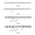
- FIG. 9is a flow chart explaining an exemplary fabrication method for the semiconductor package shown in FIGS. 1A and 1B ;
- FIGS. 10A through 10Hare cross-sectional views illustrating an exemplary sequence of steps which may be used to facilitate the fabrication of the semiconductor package shown in FIGS. 1A and 1B ;
- FIG. 11is a flow chart explaining an exemplary fabrication method for the semiconductor package shown in FIG. 7 ;
- FIGS. 12A through 12Iare cross-sectional views illustrating an exemplary sequence of steps which may be used to facilitate the fabrication of the semiconductor package shown in FIG. 7 .
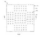
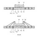
- FIG. 1Aillustrates a substrate 110 and a land 120 used for a semiconductor package 100 according to an exemplary embodiment of the present invention.
- the semiconductor package 100may include a substrate 110 , a land 120 penetrating the substrate 110 , an adhesive 130 formed on an upper portion of the substrate 110 , a semiconductor die 140 mounted on an upper portion of the adhesive 130 , a conductive wire 150 electrically coupling the land 120 and the semiconductor die 140 , an encapsulant 160 encapsulating the semiconductor die 140 and the conductive wire 150 , and a solder ball 170 formed on a lower portion of the land 120 .
- the substrate 110is preferably formed in a plate shape and is provided with an area for mounting the semiconductor die 140 .
- the substrate 110includes a patterned metal layer 111 defining a plurality of holes 111 a within the substrate 110 , and an insulation layer 112 formed along an outer portion of the patterned metal layer 111 .
- the patterned metal layer 111 formed in a plate shapeis provided with a plurality of holes 111 a as indicated above.
- the layer 111can be made of a metal alloy including one or more metals selected from metals such as copper, aluminum, nickel and the like. Accordingly, the layer 111 increases thermal conductivity of the substrate 110 , and thus heat generated from the semiconductor die 140 disposed on an upper portion of the patterned metal layer 111 as a heatproof plate is easily dissipated outside the semiconductor device 100 .
- the thickness of the substrate 110may be from about 0.2 mm to 1.0 mm for preventing warpage, but not limited thereto.
- the insulation layer 112is formed along an outer surface of the patterned metal layer 111 .
- the insulation layer 112is formed along an inner wall of the holes 111 a formed within the patterned metal layer 111 , in addition to upper and lower surfaces of the layer 111 .
- the insulation layer 112may be made of insulation resin.
- the insulation layer 112may be formed by coating, spraying, vacuum printing, or dipping the patterned metal layer 111 into a resin bath, though the present mention is not limited to any particular method for forming the insulation layer 112 . Accordingly, the insulation layer 112 allows the patterned metal layer 111 and the land 120 formed inside the holes 111 a of the patterned metal layer 111 to be electrically independent.
- Each land 120is formed by filling one of the plurality of holes 110 a collectively defined by the holes 111 a as lined with the insulation layer 112 with a prescribed conductive material. Since the insulation layer 112 is already provided inside the holes 111 a of the patterned metal layer 111 , each land 120 is thus surrounded by the insulation layer 112 . Further, each land 120 may be formed in to have a square, circular or triangular cross-sectional shape, though not being limited to these shapes. Each land 120 may be formed by selecting any one of gold, silver, copper, aluminum, solder, or combinations thereof. Further, each land 120 is exposed in the upper and lower surfaces of the substrate 110 , and the conductive wire 150 and the solder ball 170 may be connected to respective ones of the exposed portions thereof.
- the adhesive 130is formed on an upper portion of the substrate 110 .
- the adhesive 130attaches the substrate 110 to the semiconductor die 140 .
- Materials of the adhesive 130may include an epoxy, an adhesive tape or their equivalent materials, though not being limited thereto.
- the semiconductor die 140is attached to the upper portion of the substrate 110 with the adhesive 130 . Although the only one semiconductor die 140 is shown, it is contemplated that a plurality of semiconductor dies 140 can be stacked within the semiconductor package 100 . Further, the semiconductor die 140 is provided with a plurality of bond pads 141 on an upper portion thereof. Although the bond pads 141 are shown as protruding from the upper portion of the semiconductor die 140 , the bond pads 141 may be formed inside the semiconductor die 140 .
- the conductive wires 150electrically couple the bond pads 141 of the semiconductor die 140 to respective ones of the lands 120 .
- Each conductive wire 150is provided by normal wire bonding such that one end of the conductive wire 150 forms a ball bonding area on a bond pad 141 of the semiconductor die 150 , and the other end of the conductive wire 150 forms a stitch bonding area on the exposed upper portion of a corresponding land 120 .
- the conductive wire 150may be provided by standoff stitch bonding (SSB) that forms the ball bonding area on the land 120 , and connects the ball bonding area with a stud bump formed on the corresponding bond pad 141 of the semiconductor die 140 .
- SSBstandoff stitch bonding
- the encapsulant 160performs encapsulation covering the semiconductor die 140 and the conductive wire 150 .
- the encapsulant 160protects the semiconductor die 140 and the conductive wire 150 from external shock.
- the encapsulant 150may be selected from one of epoxy resin, silicone resin or equivalent materials, but is not limited thereto.
- Each solder ball 170is formed on the exposed lower portion of a corresponding land 120 . Further, each solder ball 170 may be electrically coupled with an external circuit. Each solder ball 170 can be made of a metal alloy including one or more metals selected from metals such as tin (Sn), lead (Pb) or silver (Ag) and the like, but is not limited thereto.
- the substrate 110 including the patterned metal layer 111 made of metalplays a role of a heatproof plate, thereby dissipating heat generated from the semiconductor die 140 to the outside. Additionally, the semiconductor package 100 has reduced susceptibility to warpage attributable to heat generated from the substrate 110 .
- the semiconductor package 100may have a number of the solder balls 180 commensurate to that of a conventional BGA (Ball Grid Array) package.
- the substrate 110can be formed by a relatively simple process for etching a metal layer and an insulation layer so as to save fabricating costs in relation thereto.
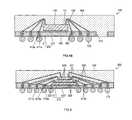
- the semiconductor 200may include a substrate 210 , at least one land 220 formed on the substrate 210 , a first semiconductor die 240 mounted to the substrate 210 , a conductive bump 242 electrically coupling the first semiconductor die 240 to the land 220 , an underfill 243 formed between the substrate 210 and the first semiconductor die 240 , a second semiconductor die 245 stacked upon an upper portion of the first semiconductor die 240 , at least one conductive wire 250 electrically coupling the second semiconductor die 245 and the land 220 , an encapsulant 160 formed on an upper portion of the substrate 210 , and at least one solder ball 270 formed on a lower portion of the substrate 210 and electrically coupled to the land 220 .
- the substrate 210may include a patterned metal layer 211 defining a plurality of holes 211 a , and having an insulation layer 212 formed along an outer portion of the patterned metal layer 211 .
- the insulation layer 212is formed inside the holes 211 a , in addition to upper and lower surfaces of the patterned metal layer 211 .
- the insulation layer 212is formed along an inner wall of each of the holes 211 a instead of completely filling the holes 211 a of the patterned metal layer 211 .
- the holes 210 a collectively defined by the holes 211 a as lined with the insulation layer 212are of sufficient size or diameter to form respective ones of the lands 220 .
- Each land 220is formed completely by filling the inside each hole 210 a of the substrate 210 with a conductive metal material.
- the lands 220are also formed in areas of the substrate 210 so as to be operative to electrically connect the first semiconductor die 240 directly to the solder balls 270 through the use of the lands 220 .
- the structural and functional attributes of the lands 220is the same as the lands 120 in the above-described exemplary embodiment.
- the first semiconductor die 240is mounted in a flip-chip arrangement on the upper portion of the substrate 210 .
- the first semiconductor die 240is provided with bond pads 241 on one surface thereof, the bond pads 241 being arranged to be electrically coupled to respective ones of the lands 220 .
- the conductive bumps 242electrically couple the bond pads 241 of the first semiconductor die 240 to respective ones of the lands 220 .
- the conductive bumps 242connect the bond pads 241 of the first semiconductor die 240 to the lands 220 , thereby reducing the length in comparison with connection by wire and then reducing noise of inputted/outputted electric signals.
- the underfill 243is formed between the first semiconductor die 240 and the substrate 210 .
- the underfill 243is formed using epoxy, generally.
- the underfill 243reduces stress applied to the first semiconductor die 240 due to difference of the coefficient of thermal expansion between the first semiconductor die 240 and the substrate 210 .
- the second semiconductor die 245is adhered to the upper portion of the first semiconductor die 240 using an adhesive 244 .
- the second semiconductor die 245is the same as the semiconductor die 140 of the semiconductor package 100 as explained above, except that the adhesive 244 is formed on the upper portion of the first semiconductor die 241 .
- the conductive wires 250 shown in FIG. 2Belectrically couple the bond pads 246 of the second semiconductor die 245 to the lands 220 .
- the conductive wires 250are the same as the conductive wires 150 of the semiconductor package 100 as explained above, except that the conductive wires 250 are electrically connected to the second semiconductor die 245 in the semiconductor package 200 .
- the solder balls 270are formed on a lower surface of the substrate 210 and electrically coupled with respective ones of the lands 220 .
- the solder balls 270are also formed so as to input and output an electrical signal from the semiconductor package 200 .
- the solder balls 270are the same as the solder balls 170 of the semiconductor package 100 , as explained above.
- the semiconductor package 200is provided with the substrate 210 used as a heatproof plate.
- the substrate 210used as a heatproof plate.
- a thermal dissipation rate of the semiconductor die 240is increased, with warpage due to heat generated from the substrate 210 being prevented and fabrication costs for the substrate 210 being reduced.
- the substrate 210may be fabricated with a relatively simple process, and provide the same number of the solder balls 270 as a conventional BGA package.
- the substrate 210 corresponding to a filp-chip shaped semiconductor diecan reduce noise of input/output signals.
- the semiconductor package 300may include a substrate 310 , at least one land 120 , an adhesive 130 , a semiconductor die 140 , a conductive wire 150 , an encapsulant 160 and at least one solder ball 170 electrically connected to the land 120 .
- the substrate 310may include a patterned metal layer 311 defining a plurality of holes 311 a , and an insulation layer 312 formed on the patterned metal layer 311 . Further, the substrate 310 of the semiconductor package 300 is provided with at least one hole 310 a collectively defined by the hole 311 a and the insulation layer 312 for accommodating a land 120 in the same manner described above in relation to the semiconductor package 100 .
- the substrate 310may further define one or more penetration areas or openings 313 in prescribed portions thereof. Each penetration opening 313 extends through the substrate 310 , and is defined by an opening in patterned metal layer 311 which is covered or lined with the insulation layer 312 , similar to the manner in which each of the holes 310 a are formed.
- the penetration openings 313each preferably have a generally elliptical as shown, though other configurations such as a circular, triangular, square or star shape are contemplated to be within the spirit and scope of the present invention.
- Each penetration opening 313is ultimately filled with the encapsulant 160 . Accordingly, the penetration openings 313 increase a surface area in which the encapsulant 160 is engaged with the substrate 310 , thereby increasing the adhesion force between the substrate 310 and the encapsulant 160 .
- the semiconductor 300 of the present inventionis provided with the substrate 310 serving as a heatproof plate, so as to easily dissipate heat generated from the semiconductor die 140 , the substrate configuration also saving fabrication costs, preventing warpage due to heat generated from the semiconductor die 140 , and defining the same number of solder balls 170 as a conventional BGA package.
- the filling of the encapsulant 160 into the penetration opening(s) 313increases the adhesion force between the substrate 310 and the encapsulant 160 .
- the semiconductor package 400may include the substrate 410 , a plurality of lands 420 penetrating and thus extending through the substrate 410 , an adhesive 130 , a semiconductor die 140 , a conductive wire 450 electrically coupling the lands 420 to the semiconductor die 140 , an encapsulant 160 and solder balls 170 electrically coupled to respective ones of the lands 420 .
- the substrate 410is formed in a plate shape and may include a patterned metal layer 411 defining a plurality of holes 411 a , an insulation layer 412 formed on at least a portion of the patterned metal layer 411 and at least one penetration area or opening 313 penetrating or extending through the substrate 410 .
- the holes 410 a of the substrate 410which are each collectively defined by a hole 411 a as internally coated by the insulation layer 412 may be arranged in a radial pattern about a center of the substrate 410 as shown in FIG. 4A . Further, although not shown in the drawings, the holes 410 a may be arranged in a crossing pattern on the substrate 410 .
- Each land 420is formed by filling a respective one of the holes 410 a of the substrate 410 with a conductive metal material as described above in relation to other embodiments. Accordingly, the lands 420 are also arranged in a generally radial pattern or a crossing pattern about a center of the substrate 410 . The lands 420 are electrically coupled with respective ones of the conductive wires 450 , which are in turn electrically coupled to respective ones of the bond pads 141 of the semiconductor die 140 . The spacing and arrangement of the lands 420 is such that the sweeping of the conductive wires 450 may be prevented during the encapsulation process to form the encapsulant 160 , so as to prevent an electrical short or cross from being mutually generated.
- the conductive wires 450electrically couple the lands 420 to the bond pads 141 of the semiconductor die 140 .
- the lands 420are arranged in a radial pattern or a crossing pattern so that the conductive wires 450 have a maximum spacing or separation distance from each other. Accordingly, the conductive wires 450 are less susceptible to sweeping in the encapsulation process, thereby preventing an electrical short or cross from being mutually generated.
- the semiconductor package 400is provided with the substrate 410 which functions as a heatproof plate so as to dissipate heat generated from the semiconductor die 140 easily, and is less susceptible to warpage due to heat generated from the semiconductor die 140 .
- the semiconductor package 500may include a substrate 510 , at least one land 520 penetrating or extending through the substrate 510 , an adhesive 530 formed on the substrate 510 , at least one semiconductor die 540 attached to the substrate 510 with the adhesive 530 , at least one conductive wire 550 electrically coupling the semiconductor die 540 to the land 520 , an encapsulant 160 and a solder ball 170 electrically connected to the land 520 .
- the substrate 510includes a patterned metal layer 511 defining holes 511 a and an insulation layer 512 covering at least a portion of the patterned metal layer 511 .
- the substratealso includes holes 510 a which are each collectively defined by one of the holes 511 a as internally coated with the insulation layer 512 , each of the holes 510 a accommodating a respective one of the lands 520 .
- the substrate 510defines at least one step 510 b , which effectively creates a an inner portion of a first thickness, a middle portion which circumvents the inner portion and is of a second thickness exceeding the first thickness, and a peripheral outer portion which circumvents the middle portion and is of a third thickness exceeding the second thickness.
- the semiconductor die 540is mounted to the center of the inner portion of the substrate 510 .
- a plurality of lands 520is disposed in the substrate 510 within respective ones of the holes 510 a thereof.
- the holes 510 aare of differing heights, depending on which of the inner, middle and outer portions of the substrate in which they are positioned.
- certain sets or groups of the lands 520are also of differing heights or thicknesses, depending on which of the inner, middle and outer portions in which they are located.
- each land 520is formed at the same height or thickness of that portion of the substrate 510 in which it is located.
- the lands 520are electrically connected to the semiconductor die 540 by the conductive wires 550 . Accordingly, the lands 520 are elevated higher toward the outer portion of the substrate 510 , thus mitigating against the sweeping of the conductive wires 550 in the encapsulation process to prevent the conductive wires 550 from crossing or shorting.
- At least one semiconductor die 540may be mounted to the central area of the inner portion of the substrate 510 .
- the semiconductor die 540is provided with bond pads 541 in an upper portion of the semiconductor die 540 , and the semiconductor die 540 may be stacked using a portion that the bond pads 541 are not formed upon. Although three semiconductor dies 540 are stacked are shown in FIG. 5 , the present invention is not limited to any particular number or arrangement of semiconductor dies 540 .
- the conductive wires 550electrically couple the bond pads 541 of the semiconductor dies 540 to respective ones of the lands 520 . Further, the height of the lands 520 is formed to be higher toward the outer portion of the substrate 510 as indicated above, and thus the conductive wires 550 extending to the bond pads 541 may be separated from each other by a corresponding distance. Accordingly, the sweeping of the conductive wires 550 may be mitigated or prevented in the encapsulation process used to form the package body 160 , thereby preventing the conductive wires 550 from crossing or shorting.
- the semiconductor package 500is provided with the substrate 410 which serves as a heatproof plate so as to easily emit heat generated from the semiconductor die(s) 540 , and is less susceptible to warpage due to heat generated from the semiconductor die(s) 540 .
- the semiconductor package 600may include a substrate 610 , at least one land 120 , at least one lead 625 connected with a side portion of the substrate 610 , an adhesive 130 , at least one semiconductor die 140 , at least one conductive wire 650 , an encapsulant 660 and at least one solder ball 170 electrically connected to the land 120 .
- the substrate 610is generally formed in a plate shape.
- the substrate 610includes a patterned metal layer 611 which defines a plurality of holes 611 a and is at least partially covered by an insulation layer 612 .
- the substrate 610also includes a plurality of holes 610 a which are each collectively defined by a hole 611 a as internally covered or coated with the insulation layer 612 .
- Each hole 610 aaccommodates a respective one of the lands 620 .
- a peripheral portion of the substrate 610is etched on a lower portion or surface of the substrate 610 , thus forming a peripheral stepped portion 610 b which is of a reduced thickness in comparison to the remainder of the substrate 610 .
- Each lead 625is connected with the stepped portion 610 b of the substrate 610 by a tape, an adhesive or the like, and is outwardly exposed through a side portion or surface of the encapsulant 660 .
- the stepped portion 610 b of the substrate 610is covered with the insulation layer 612 and maintained in an insulated state, and thus the leads 625 can be electrically independent of the substrate 610 . Further, the leads 625 can be electrically coupled to the semiconductor die 140 by the conductive wires 650 .
- the conductive wires 650electrically couple the semiconductor die 140 to respective ones of the lands 120 . Further, as described above, the conductive wires 650 may be used to electrically couple the semiconductor die 140 to the lead 625 .
- the encapsulant 660covers the stepped portion 610 b of the substrate 610 , inner portions of the leads 625 , the semiconductor die 140 and the conductive wires 650 . Accordingly, the encapsulant 660 promotes bonding or adhesion between the stepped portion 610 b of the substrate 610 and the leads 625 . Further, as indicated above, the leads 625 protrude from a side surface of the encapsulant 660 .
- the semiconductor package 600is provided with the lead(s) 625 so as to increase the number of terminals to be connected with an external circuit. Further, the semiconductor package 600 is provided with the substrate 610 made of metal, which is used as a heatproof plate, thus allowing the heat generated from the semiconductor die 140 to be dissipated easily, while being less susceptible to warpage attributable to the heat.
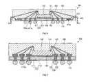
- the semiconductor package 700may include a substrate 710 , at least one rivet 720 penetrating or extending through the substrate 710 , an adhesive 130 , at least one semiconductor die 140 , at least one conductive wire 150 , an encapsulant 160 and at least one solder ball 170 electrically connected to the rivet 720 .
- the substrate 710is formed in a plate shape and is provided with a plurality of holes 710 a . Further, the substrate 710 may include a patterned metal layer 711 which defines a plurality of holes 711 a and is at least partially covered by an insulation layer 712 . Each of the holes 710 a is collectively defined by a hole 711 a and a small portion of the insulation layer 712 .
- Each rivet 720is inserted into a respective one of the holes 710 a of the substrate 710 .
- An upper portion of each rivet 720has a larger diameter rather than that of the hole 710 a of the substrate 710 , and thus the rivet 720 is fixed to the substrate 710 to prevent the rivet 720 from slipping through to a lower portion of the substrate 710 .
- Each rivet 720may include an outer insulation film 721 which directly contacts the substrate 710 and is open in both directions perpendicular to the substrate 710 , and an internal land metal layer 722 which is formed by filling the interior of the insulation film 721 with a conductive metal material. The insulation film 721 insulates the substrate 710 from the land metal layer 722 of the rivet 720 .
- the land metal layer 722has one end which is exposed to an upper portion of the substrate 710 and an opposed end which is exposed to a lower portion of the substrate 710 .
- the land metal layer 722is provided with an upper portion having a diameter larger than that of the hole 710 a of the substrate 710 so as to be fixed to the hole 710 a of the substrate 710 .
- the land metal layer 722penetrates or extends through the substrate 710 so as to input and output electrical signals through the land metal layer 722 .
- the semiconductor package 700is provided with the substrate 710 used as a heatproof plate, thereby easily dissipating heat generated from the semiconductor die 140 and being less susceptible to due to such heat. Further, the semiconductor package 700 is provided with the lands 720 within respective ones of the holes 710 a of the substrate 710 , thereby forming a conventional land, a conductive via and a conductive pattern structure in one process through a single structural element. Accordingly, the fabrication costs for the semiconductor package 700 can be saved through the resultant simplification of the process for forming lands on substrates.
- the semiconductor package 800may include a substrate 210 , at least one land 220 , a rerouting film 813 formed on an upper portion of the substrate 210 , an adhesive 130 formed on an upper portion of the rerouting film 813 , a semiconductor die 140 , at least one conductive wire 150 , an encapsulant 160 and at least one solder ball 270 electrically connected to the land 220 .
- the rerouting film 813is formed on an upper portion of the substrate 210 .
- the rerouting film 813comprises an insulation film 814 extending in parallel to the substrate 210 .
- the rerouting film 813includes a first pattern 815 formed in an upper side of the insulation film 814 , a second pattern 816 formed on a lower side of the insulation film 814 and conductive vias 817 connecting the first and second patterns 815 and 816 to each other in a prescribed pattern or arrangement.
- Each conductive via 817is formed in a vertical direction to connect the first and second patterns 815 and 816 .
- Each conductive via 817may be hollow, and formed with metal along an inner wall of the rerouting film 813 .
- each conductive via 817may be solid and formed by filling a complimentary opening in the rerouting film 813 with a conductive metal material. Further, the upper and lower portions of the rerouting film 813 may be formed with a separate polyamide layer 818 partially insulating the first and second patterns 815 and 816 .
- the first pattern 815is electrically coupled to the lands 220 and hence the solder balls 270 by the vias 817 and the second pattern 816 .
- the second pattern 816may be interfaced to the lands 220 through the use of electrical coupling members 819 .
- the configuration of the second pattern 816 and vias 817allows for the electrical of the first pattern 815 to those lands 220 positioned in the substrate 810 beneath the semiconductor die 140 .
- the first and second patterns 815 , 816are each electrically insulated from the semiconductor die 140 . However, as indicated above, the second pattern 816 is electrically coupled with the first pattern 815 by the conductive vias 817 .
- the rerouting film 813allows certain ones of the lands 220 to be formed beneath the semiconductor die 140 .
- the conductive wires 850electrically couple the bond pads 141 of the semiconductor die 140 to the first pattern 815 of the rerouting film 813 . Accordingly, the conductive wires 850 electrically couple the semiconductor die 140 to the lands 220 , and hence the solder balls 270 , via the rerouting film 813 .
- the rerouting film 813effectively routes the signals from certain ones of the conductive wires 850 to those lands 220 which are located beneath the semiconductor die 140 .
- the semiconductor package 800is provided with the substrate 210 which functions as a heatproof plate, so that the heat generated from the semiconductor die 140 is easily dissipated to the outside, with the substrate 210 also being less susceptible to warpage due to such heat. Further, the substrate 210 can be fabricated by a relatively simple process for etching a metal layer and forming an insulation layer, thus saving fabrication costs. Further, the semiconductor package 800 can be provided with a lot of input/output terminals regardless of a position of the semiconductor die 140 due to the inclusion of the rerouting film 813 .
- the fabrication method for the semiconductor package 100includes steps of providing a metal layer (S 1 ), forming a patterned metal layer (S 2 ), forming an insulation layer (S 3 ), forming a land (S 4 ), attaching a semiconductor die (S 5 ), bonding a wire (S 6 ), performing encapsulation (S 7 ) and attaching a solder ball (S 8 ).
- the steps of FIG. 9will be explained with reference to FIGS. 10A to 10H below.
- a metal layer 10 formed in a plate shapeis provided (S 1 ).
- the metal layer 10is made of a metal material having high thermal conductivity to easily emit heat generated from a semiconductor die to the outside.
- the metal layer 10can be made of copper, aluminum, nickel and their alloys.
- holes 111 aare formed on the metal layer 10 and then a patterned metal layer 111 is formed (S 2 ).
- a method for forming the holes 111 a in the metal layer 10may be accomplished by etching. Further, a mask for etching may be formed by attaching a tape or coating a photo-resist in an area except for the area to be formed with the holes 111 a in the metal layer 10 . In addition, a series of processes are performed to remove the tape or the photo-resist after etching. Further, the method for forming the holes 111 a in the metal layer 10 may be accomplished by laser drilling.
- an insulation layer 112is then formed on the patterned metal layer 111 , the patterned metal layer 111 a and the insulation layer 112 collectively forming a substrate 110 (S 3 ).
- an insulation materialmay be coated on upper and lower surfaces of the pattern metal layer 111 .
- the insulation materialis filled inside and thus coats the interior surfaces of the holes 111 a .
- a vacuum suction processmay additionally be performed to form the holes 111 a filled with the insulation material.
- the insulation layer 112may be formed on the upper and lower surfaces of the patterned metal layer 111 and along an inner wall of the holes 111 a . Holes 110 a are defined by the coating of the internal walls of the holes 111 a with the insulation layer 112 .
- the lands 120are formed in respective ones of the holes 110 a (S 4 ).
- the lands 120is formed by filling the holes 110 a of the substrate 110 with a suitable conductive metal material.
- Each land 120may be formed by electroplating after spreading a conductivity plate on a bottom of the substrate 110 and using the conductivity plate as a seed. Of course, after forming each land 120 , the conductivity plate is removed. Further, in case that each land is formed of 120 solder, the lands 120 may be formed by filling the holes 110 a using solder screen printing.
- the semiconductor die 140is attached to an upper portion of the substrate 110 (S 5 ).
- the semiconductor die 140is attached to the substrate 110 by an adhesive 130 applied to the lower surface thereof.
- the bond pads 141 of the semiconductor die 140are then electrically coupled to respective ones of the lands 120 using the conductive wires 150 (S 6 ).
- the conductive wires 150may each be formed by normal wire bonding that forms a ball bonding area on a respective one of the bond pads 141 of the semiconductor die 140 using one end of the conductive wire 150 , and forms a stitch bonding area on a respective one of the lands 120 using the other end of the conductive wire 150 .
- the ball bonding areamay formed on the land 120
- a stud bumpmay formed on the bond pad 141 of the semiconductor die 140
- the conductive wire 150may be formed using a standoff stitch bonding which connects the ball bonding area with the stud bump.
- the encapsulant 160is then formed on the upper portion of the substrate 110 (S 7 ).
- the encapsulant 160encapsulates the semiconductor die 140 and the conductive wires 150 .
- the encapsulant 160may be one selected from epoxy resin, silicone resin or equivalent materials.
- solder balls 170are then formed on the lower portion of the substrate 110 (S 8 ).
- the solder balls 170are electrically connected to respective ones of the lands 120 .
- the solder balls 170may each be made of a metal alloy including one or more metals selected from the group consisting of tin (Sn), lead (Pb), silver (Ag) or the like.
- the semiconductor package 100is provided with the substrate 110 which functions as a heatproof plate, so as to improve efficiency for emitting heat generated from the semiconductor die 140 to the outside, the substrate also being less susceptible to warpage due to such heat and defining the same number of the solder balls 170 as in a conventional BGA semiconductor package. Further, the semiconductor package 100 may be produced through a simplified manufacturing process, thus reducing fabrication costs.
- the fabrication method for the semiconductor package 700may include the steps of providing a metal layer and an insulation layer (S 1 ), forming a substrate (S 2 ), forming a rivet (S 3 ), inserting the rivet (S 4 ), opening upper and lower portions of the rivet (S 5 ), attaching a semiconductor die (S 6 ), bonding wires (S 7 ), performing encapsulation (S 8 ) and attaching a solder ball (S 9 ).
- the steps of FIG. 11will be explained with reference to FIGS. 12A to 12I below.
- the metal layer 10 and the insulation layer 20 surrounding or covering an outer portion of the metal layer 10are provided (S 1 ).
- the substrate 710 having holes 710 ais formed by etching the metal layer 10 and the insulation layer 20 (S 2 ).
- the substrate 710includes a patterned metal layer 711 and an insulation layer 712 which collectively define the holes 710 a.
- a rivet 30 including an insulation film 31 and a land metal layer 722is provided (S 3 ).
- the rivet 30has a little smaller diameter than that of each hole 710 a of the substrate 710 , and an upper portion of the rivet 30 has a larger diameter than that of each hole 710 a . Accordingly, the rivet 30 may be fixed in a prescribed position when inserted into a respective one of the holes 710 a.
- the rivets 30are inserted into respective ones of the holes 710 a of the substrate 710 (S 4 ). Each rivet 30 is inserted and fitted to a corresponding hole 710 a of the substrate 710 , and an upper portion of the rivet 30 is supported by the substrate 710 and fixed thereto.
- the upper and lower surfaces of the rivet 30are removed and an internal land metal layer 722 is exposed, thereby forming the land 720 (S 5 ).
- a process of grinding or etchingmay be performed.
- the upper and lower surfaces of the insulation film 31are removed, the land metal layer 722 is exposed, thereby forming the land 720 which is capable of inputting and outputting electrical signals.
- the semiconductor die 140is then attached to the upper portion of the substrate 710 (S 6 ).
- the semiconductor die 140is provided with a plurality of bond pads 141 in an upper portion of the semiconductor die 140 and attached to the substrate 710 through the adhesive 130 applied to a lower portion of the semiconductor die 140 .
- each conductive wire 150may be formed by normal wire bonding that forms a ball bonding area on a respective one of the bond pads 141 of the semiconductor die 140 , and forms a stitch bonding area on a respective one of the lands 720 . Additionally, although not shown in the drawings, each conductive wire 150 may be formed by standoff stitch bonding that forms a ball bonding area on the land 720 and a stud bump on the bond pad 141 , and connects them to each other.
- the semiconductor die 140 and the conductive wire 150are encapsulated by the encapsulant 160 (S 8 ).
- the encapsulantalso covers a portion of the substrate 710 .
- the encapsulant 160protects internal elements of the semiconductor package 700 and may be selected from one of epoxy resin, silicone resin or equivalent materials.
- solder balls 710are then attached to the lower portion of the substrate 710 (S 9 ).
- the solder balls 170are electrically connected to respective ones of the lands 720 , and provide a path electrically coupling the semiconductor die 140 and an external circuit.
- Each solder ball 170can be made of a metal alloy of tin (Sn), lead (Pb), silver (Ag) and the like.
- the semiconductor package 700is provided with the substrate 710 made of metal, which functions as a heatproof plate, thereby allowing the heat generated from the semiconductor die 140 to be dissipated easily to the outside, the substrate 710 also being less susceptible to warpage due to such heat, and further reducing the fabricating costs of the semiconductor package 700 .
- the lands 720are each formed by a simplified fabrication process involving the use of the rivets 30 as described above.
Landscapes
- Physics & Mathematics (AREA)
- Condensed Matter Physics & Semiconductors (AREA)
- General Physics & Mathematics (AREA)
- Engineering & Computer Science (AREA)
- Computer Hardware Design (AREA)
- Microelectronics & Electronic Packaging (AREA)
- Power Engineering (AREA)
- Geometry (AREA)
- Cooling Or The Like Of Semiconductors Or Solid State Devices (AREA)
Abstract
Description
Claims (20)
Priority Applications (1)
| Application Number | Priority Date | Filing Date | Title |
|---|---|---|---|
| US12/181,256US8125064B1 (en) | 2008-07-28 | 2008-07-28 | Increased I/O semiconductor package and method of making same |
Applications Claiming Priority (1)
| Application Number | Priority Date | Filing Date | Title |
|---|---|---|---|
| US12/181,256US8125064B1 (en) | 2008-07-28 | 2008-07-28 | Increased I/O semiconductor package and method of making same |
Publications (1)
| Publication Number | Publication Date |
|---|---|
| US8125064B1true US8125064B1 (en) | 2012-02-28 |
Family
ID=45694459
Family Applications (1)
| Application Number | Title | Priority Date | Filing Date |
|---|---|---|---|
| US12/181,256Active2030-06-09US8125064B1 (en) | 2008-07-28 | 2008-07-28 | Increased I/O semiconductor package and method of making same |
Country Status (1)
| Country | Link |
|---|---|
| US (1) | US8125064B1 (en) |
Cited By (9)
| Publication number | Priority date | Publication date | Assignee | Title |
|---|---|---|---|---|
| US20120079176A1 (en)* | 2010-06-25 | 2012-03-29 | Biwin Technology Limited | Memory device |
| US20120180312A1 (en)* | 2009-06-26 | 2012-07-19 | Zhichao Zhang | Core via for chip package and interconnect |
| US20130175072A1 (en)* | 2010-09-09 | 2013-07-11 | Texas Instruments Incorporated | Reducing thermal gradients to improve thermopile performance |
| US8742477B1 (en)* | 2010-12-06 | 2014-06-03 | Xilinx, Inc. | Elliptical through silicon vias for active interposers |
| US8921995B1 (en)* | 2008-10-20 | 2014-12-30 | Maxim Intergrated Products, Inc. | Integrated circuit package including a three-dimensional fan-out/fan-in signal routing |
| US9355947B2 (en)* | 2014-05-14 | 2016-05-31 | Samsung Electronics Co., Ltd. | Printed circuit board having traces and ball grid array package including the same |
| US9601419B1 (en)* | 2014-06-06 | 2017-03-21 | Altera Corporation | Stacked leadframe packages |
| US10134668B2 (en)* | 2017-04-07 | 2018-11-20 | Ibis Innotech Inc. | Package structure |
| US20190348387A1 (en)* | 2013-03-14 | 2019-11-14 | UTAC Headquarters Pte. Ltd. | Semiconductor packages and methods of packaging semiconductor devices |
Citations (335)
| Publication number | Priority date | Publication date | Assignee | Title |
|---|---|---|---|---|
| US2596993A (en) | 1949-01-13 | 1952-05-20 | United Shoe Machinery Corp | Method and mold for covering of eyelets by plastic injection |
| US3435815A (en) | 1966-07-15 | 1969-04-01 | Micro Tech Mfg Inc | Wafer dicer |
| US3734660A (en) | 1970-01-09 | 1973-05-22 | Tuthill Pump Co | Apparatus for fabricating a bearing device |
| US3838984A (en) | 1973-04-16 | 1974-10-01 | Sperry Rand Corp | Flexible carrier and interconnect for uncased ic chips |
| US4054238A (en) | 1976-03-23 | 1977-10-18 | Western Electric Company, Inc. | Method, apparatus and lead frame for assembling leads with terminals on a substrate |
| US4189342A (en) | 1971-10-07 | 1980-02-19 | U.S. Philips Corporation | Semiconductor device comprising projecting contact layers |
| US4221925A (en) | 1978-09-18 | 1980-09-09 | Western Electric Company, Incorporated | Printed circuit board |
| US4258381A (en) | 1977-12-07 | 1981-03-24 | Steag, Kernergie Gmbh | Lead frame for a semiconductor device suitable for mass production |
| US4289922A (en) | 1979-09-04 | 1981-09-15 | Plessey Incorporated | Integrated circuit package and lead frame |
| US4301464A (en) | 1978-08-02 | 1981-11-17 | Hitachi, Ltd. | Lead frame and semiconductor device employing the same with improved arrangement of supporting leads for securing the semiconductor supporting member |
| US4332537A (en) | 1978-07-17 | 1982-06-01 | Dusan Slepcevic | Encapsulation mold with removable cavity plates |
| US4417266A (en) | 1981-08-14 | 1983-11-22 | Amp Incorporated | Power and ground plane structure for chip carrier |
| US4451224A (en) | 1982-03-25 | 1984-05-29 | General Electric Company | Mold device for making plastic articles from resin |
| US4530152A (en) | 1982-04-01 | 1985-07-23 | Compagnie Industrielle Des Telecommunications Cit-Alcatel | Method for encapsulating semiconductor components using temporary substrates |
| US4541003A (en) | 1978-12-27 | 1985-09-10 | Hitachi, Ltd. | Semiconductor device including an alpha-particle shield |
| US4646710A (en) | 1982-09-22 | 1987-03-03 | Crystal Systems, Inc. | Multi-wafer slicing with a fixed abrasive |
| US4707724A (en) | 1984-06-04 | 1987-11-17 | Hitachi, Ltd. | Semiconductor device and method of manufacturing thereof |
| US4727633A (en) | 1985-08-08 | 1988-03-01 | Tektronix, Inc. | Method of securing metallic members together |
| US4737839A (en) | 1984-03-19 | 1988-04-12 | Trilogy Computer Development Partners, Ltd. | Semiconductor chip mounting system |
| US4756080A (en) | 1986-01-27 | 1988-07-12 | American Microsystems, Inc. | Metal foil semiconductor interconnection method |
| US4812896A (en) | 1986-11-13 | 1989-03-14 | Olin Corporation | Metal electronic package sealed with thermoplastic having a grafted metal deactivator and antioxidant |
| US4862245A (en) | 1985-04-18 | 1989-08-29 | International Business Machines Corporation | Package semiconductor chip |
| US4862246A (en) | 1984-09-26 | 1989-08-29 | Hitachi, Ltd. | Semiconductor device lead frame with etched through holes |
| US4907067A (en) | 1988-05-11 | 1990-03-06 | Texas Instruments Incorporated | Thermally efficient power device package |
| US4920074A (en) | 1987-02-25 | 1990-04-24 | Hitachi, Ltd. | Surface mount plastic package semiconductor integrated circuit, manufacturing method thereof, as well as mounting method and mounted structure thereof |
| US4935803A (en) | 1988-09-09 | 1990-06-19 | Motorola, Inc. | Self-centering electrode for power devices |
| US4942454A (en) | 1987-08-05 | 1990-07-17 | Mitsubishi Denki Kabushiki Kaisha | Resin sealed semiconductor device |
| US4987475A (en) | 1988-02-29 | 1991-01-22 | Digital Equipment Corporation | Alignment of leads for ceramic integrated circuit packages |
| US5018003A (en) | 1988-10-20 | 1991-05-21 | Mitsubishi Denki Kabushiki Kaisha | Lead frame and semiconductor device |
| US5029386A (en) | 1990-09-17 | 1991-07-09 | Hewlett-Packard Company | Hierarchical tape automated bonding method |
| US5041902A (en) | 1989-12-14 | 1991-08-20 | Motorola, Inc. | Molded electronic package with compression structures |
| US5057900A (en) | 1988-10-17 | 1991-10-15 | Semiconductor Energy Laboratory Co., Ltd. | Electronic device and a manufacturing method for the same |
| US5059379A (en) | 1987-07-20 | 1991-10-22 | Mitsubishi Denki Kabushiki Kaisha | Method of resin sealing semiconductor devices |
| US5065223A (en) | 1989-05-31 | 1991-11-12 | Fujitsu Vlsi Limited | Packaged semiconductor device |
| US5070039A (en) | 1989-04-13 | 1991-12-03 | Texas Instruments Incorporated | Method of making an integrated circuit using a pre-served dam bar to reduce mold flash and to facilitate flash removal |
| US5087961A (en) | 1987-01-28 | 1992-02-11 | Lsi Logic Corporation | Semiconductor device package |
| US5091341A (en) | 1989-05-22 | 1992-02-25 | Kabushiki Kaisha Toshiba | Method of sealing semiconductor device with resin by pressing a lead frame to a heat sink using an upper mold pressure member |
| US5096852A (en) | 1988-06-02 | 1992-03-17 | Burr-Brown Corporation | Method of making plastic encapsulated multichip hybrid integrated circuits |
| US5118298A (en) | 1991-04-04 | 1992-06-02 | Advanced Interconnections Corporation | Through hole mounting of integrated circuit adapter leads |
| US5122860A (en) | 1987-08-26 | 1992-06-16 | Matsushita Electric Industrial Co., Ltd. | Integrated circuit device and manufacturing method thereof |
| US5134773A (en) | 1989-05-26 | 1992-08-04 | Gerard Lemaire | Method for making a credit card containing a microprocessor chip |
| US5151039A (en) | 1990-04-06 | 1992-09-29 | Advanced Interconnections Corporation | Integrated circuit adapter having gullwing-shaped leads |
| US5157480A (en) | 1991-02-06 | 1992-10-20 | Motorola, Inc. | Semiconductor device having dual electrical contact sites |
| US5157475A (en) | 1988-07-08 | 1992-10-20 | Oki Electric Industry Co., Ltd. | Semiconductor device having a particular conductive lead structure |
| US5168368A (en) | 1991-05-09 | 1992-12-01 | International Business Machines Corporation | Lead frame-chip package with improved configuration |
| US5172214A (en) | 1991-02-06 | 1992-12-15 | Motorola, Inc. | Leadless semiconductor device and method for making the same |
| US5172213A (en) | 1991-05-23 | 1992-12-15 | At&T Bell Laboratories | Molded circuit package having heat dissipating post |
| US5175060A (en) | 1989-07-01 | 1992-12-29 | Ibiden Co., Ltd. | Leadframe semiconductor-mounting substrate having a roughened adhesive conductor circuit substrate and method of producing the same |
| US5200809A (en) | 1991-09-27 | 1993-04-06 | Vlsi Technology, Inc. | Exposed die-attach heatsink package |
| US5200362A (en) | 1989-09-06 | 1993-04-06 | Motorola, Inc. | Method of attaching conductive traces to an encapsulated semiconductor die using a removable transfer film |
| US5216278A (en) | 1990-12-04 | 1993-06-01 | Motorola, Inc. | Semiconductor device having a pad array carrier package |
| US5214845A (en) | 1992-05-11 | 1993-06-01 | Micron Technology, Inc. | Method for producing high speed integrated circuits |
| US5218231A (en) | 1989-08-30 | 1993-06-08 | Kabushiki Kaisha Toshiba | Mold-type semiconductor device |
| US5221642A (en) | 1991-08-15 | 1993-06-22 | Staktek Corporation | Lead-on-chip integrated circuit fabrication method |
| US5250841A (en) | 1992-04-06 | 1993-10-05 | Motorola, Inc. | Semiconductor device with test-only leads |
| US5252853A (en) | 1991-09-19 | 1993-10-12 | Mitsubishi Denki Kabushiki Kaisha | Packaged semiconductor device having tab tape and particular power distribution lead structure |
| US5258094A (en) | 1991-09-18 | 1993-11-02 | Nec Corporation | Method for producing multilayer printed wiring boards |
| US5266834A (en) | 1989-03-13 | 1993-11-30 | Hitachi Ltd. | Semiconductor device and an electronic device with the semiconductor devices mounted thereon |
| US5277972A (en) | 1988-09-29 | 1994-01-11 | Tomoegawa Paper Co., Ltd. | Adhesive tapes |
| US5278446A (en) | 1992-07-06 | 1994-01-11 | Motorola, Inc. | Reduced stress plastic package |
| US5279029A (en) | 1990-08-01 | 1994-01-18 | Staktek Corporation | Ultra high density integrated circuit packages method |
| US5281849A (en) | 1991-05-07 | 1994-01-25 | Singh Deo Narendra N | Semiconductor package with segmented lead frame |
| US5285352A (en) | 1992-07-15 | 1994-02-08 | Motorola, Inc. | Pad array semiconductor device with thermal conductor and process for making the same |
| US5294897A (en) | 1992-07-20 | 1994-03-15 | Mitsubishi Denki Kabushiki Kaisha | Microwave IC package |
| US5327008A (en) | 1993-03-22 | 1994-07-05 | Motorola Inc. | Semiconductor device having universal low-stress die support and method for making the same |
| US5332864A (en) | 1991-12-27 | 1994-07-26 | Vlsi Technology, Inc. | Integrated circuit package having an interposer |
| US5336931A (en) | 1993-09-03 | 1994-08-09 | Motorola, Inc. | Anchoring method for flow formed integrated circuit covers |
| US5335771A (en) | 1990-09-25 | 1994-08-09 | R. H. Murphy Company, Inc. | Spacer trays for stacking storage trays with integrated circuits |
| US5343076A (en) | 1990-07-21 | 1994-08-30 | Mitsui Petrochemical Industries, Ltd. | Semiconductor device with an airtight space formed internally within a hollow package |
| US5358905A (en) | 1993-04-02 | 1994-10-25 | Texas Instruments Incorporated | Semiconductor device having die pad locking to substantially reduce package cracking |
| US5365106A (en) | 1992-10-27 | 1994-11-15 | Kabushiki Kaisha Toshiba | Resin mold semiconductor device |
| US5381042A (en) | 1992-03-31 | 1995-01-10 | Amkor Electronics, Inc. | Packaged integrated circuit including heat slug having an exposed surface |
| EP0393997B1 (en) | 1989-04-20 | 1995-02-01 | Honeywell Inc. | Method of providing a variable-pitch leadframe assembly |
| US5391439A (en) | 1990-09-27 | 1995-02-21 | Dai Nippon Printing Co., Ltd. | Leadframe adapted to support semiconductor elements |
| US5397917A (en)* | 1993-04-26 | 1995-03-14 | Motorola, Inc. | Semiconductor package capable of spreading heat |
| US5406124A (en) | 1992-12-04 | 1995-04-11 | Mitsui Toatsu Chemicals, Inc. | Insulating adhesive tape, and lead frame and semiconductor device employing the tape |
| US5410180A (en) | 1992-07-28 | 1995-04-25 | Shinko Electric Industries Co., Ltd. | Metal plane support for multi-layer lead frames and a process for manufacturing such frames |
| US5414299A (en) | 1993-09-24 | 1995-05-09 | Vlsi Technology, Inc. | Semi-conductor device interconnect package assembly for improved package performance |
| US5417905A (en) | 1989-05-26 | 1995-05-23 | Esec (Far East) Limited | Method of making a card having decorations on both faces |
| US5428248A (en) | 1992-08-21 | 1995-06-27 | Goldstar Electron Co., Ltd. | Resin molded semiconductor package |
| US5435057A (en) | 1990-10-30 | 1995-07-25 | International Business Machines Corporation | Interconnection method and structure for organic circuit boards |
| US5444301A (en) | 1993-06-23 | 1995-08-22 | Goldstar Electron Co. Ltd. | Semiconductor package and method for manufacturing the same |
| US5452511A (en) | 1993-11-04 | 1995-09-26 | Chang; Alexander H. C. | Composite lead frame manufacturing method |
| US5454905A (en) | 1994-08-09 | 1995-10-03 | National Semiconductor Corporation | Method for manufacturing fine pitch lead frame |
| US5467032A (en) | 1993-11-09 | 1995-11-14 | Samsung Electronics Co., Ltd. | Word line driver circuit for a semiconductor memory device |
| US5474958A (en) | 1993-05-04 | 1995-12-12 | Motorola, Inc. | Method for making semiconductor device having no die supporting surface |
| US5484274A (en) | 1992-11-24 | 1996-01-16 | Neu Dynamics Corp. | Encapsulation molding equipment |
| US5493151A (en) | 1993-07-15 | 1996-02-20 | Kabushiki Kaisha Toshiba | Semiconductor device, lead frame and method for manufacturing semiconductor devices |
| US5508556A (en) | 1994-09-02 | 1996-04-16 | Motorola, Inc. | Leaded semiconductor device having accessible power supply pad terminals |
| US5517056A (en) | 1993-09-30 | 1996-05-14 | Motorola, Inc. | Molded carrier ring leadframe having a particular resin injecting area design for gate removal and semiconductor device employing the same |
| US5521429A (en) | 1993-11-25 | 1996-05-28 | Sanyo Electric Co., Ltd. | Surface-mount flat package semiconductor device |
| US5528076A (en) | 1995-02-01 | 1996-06-18 | Motorola, Inc. | Leadframe having metal impregnated silicon carbide mounting area |
| US5534467A (en) | 1993-03-18 | 1996-07-09 | Lsi Logic Corporation | Semiconductor packages for high I/O semiconductor dies |
| US5539251A (en) | 1992-05-11 | 1996-07-23 | Micron Technology, Inc. | Tie bar over chip lead frame design |
| US5543657A (en) | 1994-10-07 | 1996-08-06 | International Business Machines Corporation | Single layer leadframe design with groundplane capability |
| US5544412A (en) | 1994-05-24 | 1996-08-13 | Motorola, Inc. | Method for coupling a power lead to a bond pad in an electronic module |
| US5545923A (en) | 1993-10-22 | 1996-08-13 | Lsi Logic Corporation | Semiconductor device assembly with minimized bond finger connections |
| US5581122A (en) | 1994-10-25 | 1996-12-03 | Industrial Technology Research Institute | Packaging assembly with consolidated common voltage connections for integrated circuits |
| US5592025A (en) | 1992-08-06 | 1997-01-07 | Motorola, Inc. | Pad array semiconductor device |
| US5592019A (en) | 1994-04-19 | 1997-01-07 | Mitsubishi Denki Kabushiki Kaisha | Semiconductor device and module |
| US5594274A (en) | 1993-07-01 | 1997-01-14 | Nec Corporation | Lead frame for use in a semiconductor device and method of manufacturing the semiconductor device using the same |
| US5595934A (en) | 1995-05-17 | 1997-01-21 | Samsung Electronics Co., Ltd. | Method for forming oxide protective film on bonding pads of semiconductor chips by UV/O3 treatment |
| US5604376A (en) | 1994-06-30 | 1997-02-18 | Digital Equipment Corporation | Paddleless molded plastic semiconductor chip package |
| US5608265A (en) | 1993-03-17 | 1997-03-04 | Hitachi, Ltd. | Encapsulated semiconductor device package having holes for electrically conductive material |
| US5608267A (en) | 1992-09-17 | 1997-03-04 | Olin Corporation | Molded plastic semiconductor package including heat spreader |
| US5625222A (en) | 1993-11-18 | 1997-04-29 | Fujitsu Limited | Semiconductor device in a resin package housed in a frame having high thermal conductivity |
| US5633528A (en) | 1994-05-25 | 1997-05-27 | Texas Instruments Incorporated | Lead frame structure for IC devices with strengthened encapsulation adhesion |
| US5637922A (en) | 1994-02-07 | 1997-06-10 | General Electric Company | Wireless radio frequency power semiconductor devices using high density interconnect |
| US5639990A (en) | 1992-06-05 | 1997-06-17 | Mitsui Toatsu Chemicals, Inc. | Solid printed substrate and electronic circuit package using the same |
| US5640047A (en) | 1995-09-25 | 1997-06-17 | Mitsui High-Tec, Inc. | Ball grid assembly type semiconductor device having a heat diffusion function and an electric and magnetic shielding function |
| US5641997A (en) | 1993-09-14 | 1997-06-24 | Kabushiki Kaisha Toshiba | Plastic-encapsulated semiconductor device |
| US5644169A (en) | 1993-03-04 | 1997-07-01 | Goldstar Electron Co., Ltd. | Mold and method for manufacturing a package for a semiconductor chip and the package manufactured thereby |
| US5643433A (en) | 1992-12-23 | 1997-07-01 | Shinko Electric Industries Co., Ltd. | Lead frame and method for manufacturing same |
| US5646831A (en) | 1995-12-28 | 1997-07-08 | Vlsi Technology, Inc. | Electrically enhanced power quad flat pack arrangement |
| US5650663A (en) | 1995-07-03 | 1997-07-22 | Olin Corporation | Electronic package with improved thermal properties |
| US5661088A (en) | 1996-01-11 | 1997-08-26 | Motorola, Inc. | Electronic component and method of packaging |
| US5665996A (en) | 1994-12-30 | 1997-09-09 | Siliconix Incorporated | Vertical power mosfet having thick metal layer to reduce distributed resistance |
| EP0794572A2 (en) | 1996-03-07 | 1997-09-10 | Matsushita Electronics Corporation | Electronic component, method for making the same, and lead frame and mold assembly for use therein |
| US5673479A (en) | 1993-12-20 | 1997-10-07 | Lsi Logic Corporation | Method for mounting a microelectronic circuit peripherally-leaded package including integral support member with spacer |
| US5683943A (en) | 1994-06-14 | 1997-11-04 | Dai Nippon Printing Co., Ltd. | Process for etching a semiconductor lead frame |
| US5683806A (en) | 1988-09-29 | 1997-11-04 | Tomoegawa Paper Co., Ltd. | Adhesive tapes |
| US5689135A (en) | 1995-12-19 | 1997-11-18 | Micron Technology, Inc. | Multi-chip device and method of fabrication employing leads over and under processes |
| US5696666A (en) | 1995-10-11 | 1997-12-09 | Motorola, Inc. | Low profile exposed die chip carrier package |
| US5701034A (en) | 1994-05-03 | 1997-12-23 | Amkor Electronics, Inc. | Packaged semiconductor die including heat sink with locking feature |
| US5703407A (en) | 1995-02-14 | 1997-12-30 | Kabushiki Kaisha Toshiba | Resin-sealed type semiconductor device |
| US5710064A (en) | 1994-08-16 | 1998-01-20 | Samsung Electronics Co., Ltd. | Method for manufacturing a semiconductor package |
| US5723899A (en) | 1994-08-30 | 1998-03-03 | Amkor Electronics, Inc. | Semiconductor lead frame having connection bar and guide rings |
| US5724233A (en) | 1993-07-09 | 1998-03-03 | Fujitsu Limited | Semiconductor device having first and second semiconductor chips with a gap therebetween, a die stage in the gap and associated lead frames disposed in a package, the lead frames providing electrical connections from the chips to an exterior of the packag |
| US5726493A (en) | 1994-06-13 | 1998-03-10 | Fujitsu Limited | Semiconductor device and semiconductor device unit having ball-grid-array type package structure |
| US5736432A (en) | 1996-09-20 | 1998-04-07 | National Semiconductor Corporation | Lead frame with lead finger locking feature and method for making same |
| US5745984A (en) | 1995-07-10 | 1998-05-05 | Martin Marietta Corporation | Method for making an electronic module |
| US5753977A (en) | 1996-03-22 | 1998-05-19 | Mitsubishi Denki Kabushiki Kaisha | Semiconductor device and lead frame therefor |
| US5753532A (en) | 1995-08-30 | 1998-05-19 | Samsung Electronics Co., Ltd. | Method of manufacturing semiconductor chip package |
| EP0844665A2 (en) | 1996-11-21 | 1998-05-27 | Texas Instruments Incorporated | Wafer level packaging |
| US5766972A (en) | 1994-06-02 | 1998-06-16 | Mitsubishi Denki Kabushiki Kaisha | Method of making resin encapsulated semiconductor device with bump electrodes |
| US5770888A (en) | 1995-12-29 | 1998-06-23 | Lg Semicon Co., Ltd. | Integrated chip package with reduced dimensions and leads exposed from the top and bottom of the package |
| US5776798A (en) | 1996-09-04 | 1998-07-07 | Motorola, Inc. | Semiconductor package and method thereof |
| DE19734794A1 (en) | 1997-01-09 | 1998-07-16 | Mitsubishi Electric Corp | Wiring part and lead frame with the wiring part |
| US5783861A (en) | 1994-03-29 | 1998-07-21 | Lg Semicon Co., Ltd. | Semiconductor package and lead frame |
| US5801440A (en) | 1995-10-10 | 1998-09-01 | Acc Microelectronics Corporation | Chip package board having utility rings |
| US5814881A (en) | 1996-12-20 | 1998-09-29 | Lsi Logic Corporation | Stacked integrated chip package and method of making same |
| US5814883A (en) | 1995-10-04 | 1998-09-29 | Mitsubishi Denki Kabushiki Kaisha | Packaged semiconductor chip |
| US5814884A (en) | 1996-10-24 | 1998-09-29 | International Rectifier Corporation | Commonly housed diverse semiconductor die |
| US5818105A (en) | 1994-07-22 | 1998-10-06 | Nec Corporation | Semiconductor device with plastic material covering a semiconductor chip mounted on a substrate of the device |
| US5817540A (en) | 1996-09-20 | 1998-10-06 | Micron Technology, Inc. | Method of fabricating flip-chip on leads devices and resulting assemblies |
| US5821457A (en) | 1994-03-11 | 1998-10-13 | The Panda Project | Semiconductor die carrier having a dielectric epoxy between adjacent leads |
| US5821615A (en) | 1995-12-06 | 1998-10-13 | Lg Semicon Co., Ltd. | Semiconductor chip package having clip-type outlead and fabrication method of same |
| US5834830A (en) | 1995-12-18 | 1998-11-10 | Lg Semicon Co., Ltd. | LOC (lead on chip) package and fabricating method thereof |
| US5835988A (en) | 1996-03-27 | 1998-11-10 | Mitsubishi Denki Kabushiki Kaisha | Packed semiconductor device with wrap around external leads |
| US5844306A (en) | 1995-09-28 | 1998-12-01 | Mitsubishi Denki Kabushiki Kaisha | Die pad structure for solder bonding |
| US5854512A (en) | 1996-09-20 | 1998-12-29 | Vlsi Technology, Inc. | High density leaded ball-grid array package |
| US5856911A (en) | 1996-11-12 | 1999-01-05 | National Semiconductor Corporation | Attachment assembly for integrated circuits |
| US5859471A (en) | 1992-11-17 | 1999-01-12 | Shinko Electric Industries Co., Ltd. | Semiconductor device having tab tape lead frame with reinforced outer leads |
| US5866939A (en) | 1996-01-21 | 1999-02-02 | Anam Semiconductor Inc. | Lead end grid array semiconductor package |
| US5866942A (en) | 1995-04-28 | 1999-02-02 | Nec Corporation | Metal base package for a semiconductor device |
| US5871782A (en) | 1995-12-30 | 1999-02-16 | Lg Semicon Co. Ltd. | Transfer molding apparatus having laminated chase block |
| US5874784A (en) | 1995-10-25 | 1999-02-23 | Sharp Kabushiki Kaisha | Semiconductor device having external connection terminals provided on an interconnection plate and fabrication process therefor |
| US5877043A (en) | 1996-02-01 | 1999-03-02 | International Business Machines Corporation | Electronic package with strain relief means and method of making |
| US5886397A (en) | 1996-09-05 | 1999-03-23 | International Rectifier Corporation | Crushable bead on lead finger side surface to improve moldability |
| KR100220154B1 (en) | 1996-04-01 | 1999-09-01 | 김규현 | Method manufacture of semiconductor package |
| US5973935A (en) | 1997-04-07 | 1999-10-26 | Micron Technology, Inc. | Interdigitated leads-over-chip lead frame for supporting an integrated circuit die |
| US5977630A (en) | 1997-08-15 | 1999-11-02 | International Rectifier Corp. | Plural semiconductor die housed in common package with split heat sink |
| JP2000150765A (en) | 1998-10-21 | 2000-05-30 | Amkor Technology Inc | Semiconductor integrated circuit plastic package, ultra- compact lead frame for manufacture thereof, and its manufacture |
| USRE36773E (en) | 1993-10-18 | 2000-07-11 | Motorola, Inc. | Method for plating using nested plating buses and semiconductor device having the same |
| US6097089A (en)* | 1998-01-28 | 2000-08-01 | Mitsubishi Gas Chemical Company, Inc. | Semiconductor plastic package, metal plate for said package, and method of producing copper-clad board for said package |
| US6107679A (en) | 1997-12-22 | 2000-08-22 | Oki Electric Industry Co., Ltd. | Semiconductor device |
| US6143981A (en) | 1998-06-24 | 2000-11-07 | Amkor Technology, Inc. | Plastic integrated circuit package and method and leadframe for making the package |
| KR20000072714A (en) | 2000-09-21 | 2000-12-05 | 이희영 | Mandibular angle retractor |
| US6166430A (en) | 1998-05-27 | 2000-12-26 | Matsushita Electronics Corporation | Lead frame, method for manufacturing the frame, resin-molded semiconductor device and method for manufacturing the device |
| US6169329B1 (en) | 1996-04-02 | 2001-01-02 | Micron Technology, Inc. | Semiconductor devices having interconnections using standardized bonding locations and methods of designing |
| US6177718B1 (en) | 1998-04-28 | 2001-01-23 | Kabushiki Kaisha Toshiba | Resin-sealed semiconductor device |
| US6181002B1 (en) | 1998-12-22 | 2001-01-30 | Sharp Kabushiki Kaisha | Semiconductor device having a plurality of semiconductor chips |
| US6184465B1 (en) | 1998-11-12 | 2001-02-06 | Micron Technology, Inc. | Semiconductor package |
| US6184573B1 (en) | 1999-05-13 | 2001-02-06 | Siliconware Precision Industries Co., Ltd. | Chip packaging |
| US6194777B1 (en) | 1998-06-27 | 2001-02-27 | Texas Instruments Incorporated | Leadframes with selective palladium plating |
| US6197615B1 (en) | 1997-04-04 | 2001-03-06 | Samsung Electronics Co., Ltd. | Method of producing lead frame having uneven surfaces |
| US6198171B1 (en) | 1999-12-30 | 2001-03-06 | Siliconware Precision Industries Co., Ltd. | Thermally enhanced quad flat non-lead package of semiconductor |
| US6201186B1 (en) | 1998-06-29 | 2001-03-13 | Motorola, Inc. | Electronic component assembly and method of making the same |
| US6201292B1 (en) | 1997-04-02 | 2001-03-13 | Dai Nippon Insatsu Kabushiki Kaisha | Resin-sealed semiconductor device, circuit member used therefor |
| US6204554B1 (en) | 1996-09-05 | 2001-03-20 | International Rectifier Corporation | Surface mount semiconductor package |
| US6208020B1 (en) | 1999-02-24 | 2001-03-27 | Matsushita Electronics Corporation | Leadframe for use in manufacturing a resin-molded semiconductor device |
| US6208021B1 (en) | 1996-03-27 | 2001-03-27 | Oki Electric Industry Co., Ltd. | Semiconductor device, manufacturing method thereof and aggregate type semiconductor device |
| US6208023B1 (en) | 1997-07-31 | 2001-03-27 | Matsushita Electronics Corporation | Lead frame for use with an RF powered semiconductor |
| US6211462B1 (en) | 1998-11-05 | 2001-04-03 | Texas Instruments Incorporated | Low inductance power package for integrated circuits |
| US6218731B1 (en) | 1999-05-21 | 2001-04-17 | Siliconware Precision Industries Co., Ltd. | Tiny ball grid array package |
| US6222259B1 (en) | 1998-09-15 | 2001-04-24 | Hyundai Electronics Industries Co., Ltd. | Stack package and method of fabricating the same |
| US6222258B1 (en) | 1996-11-11 | 2001-04-24 | Fujitsu Limited | Semiconductor device and method for producing a semiconductor device |
| US6225146B1 (en) | 1996-12-24 | 2001-05-01 | Matsushita Electronics Corporation | Lead frame, method of manufacturing lead frame, semiconductor device and method of manufacturing semiconductor device |
| US6229200B1 (en) | 1998-06-10 | 2001-05-08 | Asat Limited | Saw-singulated leadless plastic chip carrier |
| US6229205B1 (en) | 1997-06-30 | 2001-05-08 | Samsung Electronics Co., Ltd. | Semiconductor device package having twice-bent tie bar and small die pad |
| US6239367B1 (en) | 1999-01-29 | 2001-05-29 | United Microelectronics Corp. | Multi-chip chip scale package |
| US6239384B1 (en) | 1995-09-18 | 2001-05-29 | Tessera, Inc. | Microelectric lead structures with plural conductors |
| JP3177060B2 (en) | 1992-04-13 | 2001-06-18 | 株式会社リコー | Reversible thermosensitive recording label and card |
| US6256200B1 (en) | 1999-05-27 | 2001-07-03 | Allen K. Lam | Symmetrical package for semiconductor die |
| US6258629B1 (en) | 1999-08-09 | 2001-07-10 | Amkor Technology, Inc. | Electronic device package and leadframe and method for making the package |
| US20010008305A1 (en) | 1998-06-10 | 2001-07-19 | Asat Ltd. | Leadless plastic chip carrier with etch back pad singulation |
| EP0459493B1 (en) | 1990-06-01 | 2001-08-16 | Kabushiki Kaisha Toshiba | A semiconductor device comprising a TAB tape and its manufacturing method |
| US20010014538A1 (en) | 1998-06-10 | 2001-08-16 | Asat Ltd. | Leadless plastic chip carrier with etch back pad singulation and die attach pad array |
| US6281566B1 (en) | 1996-09-30 | 2001-08-28 | Sgs-Thomson Microelectronics S.R.L. | Plastic package for electronic devices |
| US6282094B1 (en) | 1999-04-12 | 2001-08-28 | Siliconware Precision Industries, Co., Ltd. | Ball-grid array integrated circuit package with an embedded type of heat-dissipation structure and method of manufacturing the same |
| US6282095B1 (en) | 1999-02-02 | 2001-08-28 | Compaq Computer Corporation | Method and system for controlling radio frequency radiation in microelectronic packages using heat dissipation structures |
| US6285075B1 (en) | 1998-11-02 | 2001-09-04 | Asat, Limited | Integrated circuit package with bonding planes on a ceramic ring using an adhesive assembly |
| US6291273B1 (en) | 1996-12-26 | 2001-09-18 | Hitachi, Ltd. | Plastic molded type semiconductor device and fabrication process thereof |
| US6291271B1 (en) | 1999-09-14 | 2001-09-18 | Advanced Semiconductor Engineering, Inc. | Method of making semiconductor chip package |
| US6294100B1 (en) | 1998-06-10 | 2001-09-25 | Asat Ltd | Exposed die leadless plastic chip carrier |
| US6294830B1 (en) | 1996-04-18 | 2001-09-25 | Tessera, Inc. | Microelectronic assembly with conductive terminals having an exposed surface through a dielectric layer |
| US6295977B1 (en) | 1998-11-05 | 2001-10-02 | Wacker Chemie Gmbh | Method and device for simultaneously cutting off a multiplicity of wafers from a workpiece |
| US6297548B1 (en) | 1998-06-30 | 2001-10-02 | Micron Technology, Inc. | Stackable ceramic FBGA for high thermal applications |
| US6303984B1 (en) | 1997-08-12 | 2001-10-16 | Micron Technology, Inc. | Lead frame including angle iron tie bar |
| US6303997B1 (en) | 1998-04-08 | 2001-10-16 | Anam Semiconductor, Inc. | Thin, stackable semiconductor packages |
| US6307272B1 (en) | 1998-05-27 | 2001-10-23 | Hitachi, Ltd. | Semiconductor device and method for manufacturing the same |
| US6309909B1 (en) | 1998-07-02 | 2001-10-30 | Mitsubishi Denki Kabushiki Kaisha | Semiconductor device and method of manufacturing the same |
| US6316822B1 (en) | 1998-09-16 | 2001-11-13 | Texas Instruments Incorporated | Multichip assembly semiconductor |
| US6316838B1 (en) | 1999-10-29 | 2001-11-13 | Fujitsu Limited | Semiconductor device |
| US6323550B1 (en) | 1995-06-06 | 2001-11-27 | Analog Devices, Inc. | Package for sealing an integrated circuit die |
| US6326678B1 (en) | 1993-09-03 | 2001-12-04 | Asat, Limited | Molded plastic package with heat sink and enhanced electrical performance |
| US6326243B1 (en) | 1995-08-15 | 2001-12-04 | Kabushiki Kaisha Toshiba | Resin sealed semiconductor device including a die pad uniformly having heat conducting paths and circulating holes for fluid resin |
| US6326244B1 (en) | 1998-09-03 | 2001-12-04 | Micron Technology, Inc. | Method of making a cavity ball grid array apparatus |
| US6335564B1 (en) | 1998-05-06 | 2002-01-01 | Conexant Systems, Inc. | Single Paddle having a semiconductor device and a passive electronic component |
| US6337510B1 (en) | 2000-11-17 | 2002-01-08 | Walsin Advanced Electronics Ltd | Stackable QFN semiconductor package |
| US6339255B1 (en) | 1998-10-24 | 2002-01-15 | Hyundai Electronics Industries Co., Ltd. | Stacked semiconductor chips in a single semiconductor package |
| US20020011654A1 (en) | 2000-07-25 | 2002-01-31 | Naoto Kimura | Semiconductor device |
| US6348726B1 (en) | 2001-01-18 | 2002-02-19 | National Semiconductor Corporation | Multi row leadless leadframe package |
| US20020024122A1 (en) | 2000-08-25 | 2002-02-28 | Samsung Electronics Co., Ltd. | Lead frame having a side ring pad and semiconductor chip package including the same |
| US20020027297A1 (en) | 2000-09-04 | 2002-03-07 | Chikao Ikenaga | Semiconductor package |
| US6355502B1 (en) | 2000-04-25 | 2002-03-12 | National Science Council | Semiconductor package and method for making the same |
| US6359221B1 (en) | 1997-08-04 | 2002-03-19 | Dai Nippon Insatsu Kabushiki Kaisha | Resin sealed semiconductor device, circuit member for use therein |
| US6362525B1 (en) | 1999-11-09 | 2002-03-26 | Cypress Semiconductor Corp. | Circuit structure including a passive element formed within a grid array substrate and method for making the same |
| US20020038873A1 (en) | 2000-09-29 | 2002-04-04 | Michiaki Hiyoshi | Semiconductor device including intermediate wiring element |
| US6369454B1 (en) | 1998-12-31 | 2002-04-09 | Amkor Technology, Inc. | Semiconductor package and method for fabricating the same |
| US6369447B2 (en) | 1998-04-20 | 2002-04-09 | Mitsubishi Denki Kabushiki Kaisha | Plastic-packaged semiconductor device including a plurality of chips |
| US6373127B1 (en) | 1998-09-29 | 2002-04-16 | Texas Instruments Incorporated | Integrated capacitor on the back of a chip |
| US6376908B1 (en)* | 1997-12-10 | 2002-04-23 | Mitsubishi Gas Chemical Company, Inc. | Semiconductor plastic package and process for the production thereof |
| US6377464B1 (en) | 1999-01-29 | 2002-04-23 | Conexant Systems, Inc. | Multiple chip module with integrated RF capabilities |
| US6380048B1 (en) | 2001-08-02 | 2002-04-30 | St Assembly Test Services Pte Ltd | Die paddle enhancement for exposed pad in semiconductor packaging |
| US6384472B1 (en) | 2000-03-24 | 2002-05-07 | Siliconware Precision Industries Co., Ltd | Leadless image sensor package structure and method for making the same |
| US6388336B1 (en) | 1999-09-15 | 2002-05-14 | Texas Instruments Incorporated | Multichip semiconductor assembly |
| US6395578B1 (en) | 1999-05-20 | 2002-05-28 | Amkor Technology, Inc. | Semiconductor package and method for fabricating the same |
| US6400004B1 (en) | 2000-08-17 | 2002-06-04 | Advanced Semiconductor Engineering, Inc. | Leadless semiconductor package |
| US6399415B1 (en) | 2000-03-20 | 2002-06-04 | National Semiconductor Corporation | Electrical isolation in panels of leadless IC packages |
| US6400010B1 (en)* | 1998-02-17 | 2002-06-04 | Seiko Epson Corporation | Substrate including a metal portion and a resin portion |
| US20020072147A1 (en) | 2000-10-24 | 2002-06-13 | Murata Manufacturing Co., Ltd. | High-frequency circuit board unit, high frequency module using the same unit, electronic apparatus using the same module, and manufacturing method for the high-frequency circuit board unit |
| US6410979B2 (en) | 1998-12-21 | 2002-06-25 | Nec Corporation | Ball-grid-array semiconductor device with protruding terminals |
| KR20020049944A (en) | 2000-12-20 | 2002-06-26 | 박종섭 | semiconductor package and method for fabricating the same |
| US6414385B1 (en) | 1999-11-08 | 2002-07-02 | Siliconware Precisionindustries Co., Ltd. | Quad flat non-lead package of semiconductor |
| US6421013B1 (en) | 1999-10-04 | 2002-07-16 | Amerasia International Technology, Inc. | Tamper-resistant wireless article including an antenna |
| US6420779B1 (en) | 1999-09-14 | 2002-07-16 | St Assembly Test Services Ltd. | Leadframe based chip scale package and method of producing the same |
| US6429508B1 (en) | 2000-08-09 | 2002-08-06 | Kostat Semiconductor Co., Ltd. | Semiconductor package having implantable conductive lands and method for manufacturing the same |
| US20020111009A1 (en) | 2001-02-15 | 2002-08-15 | Megic Corporation | Reliable metal bumps on top of I/O pads after removal of test probe marks |
| US6437429B1 (en) | 2001-05-11 | 2002-08-20 | Walsin Advanced Electronics Ltd | Semiconductor package with metal pads |
| US6444499B1 (en) | 2000-03-30 | 2002-09-03 | Amkor Technology, Inc. | Method for fabricating a snapable multi-package array substrate, snapable multi-package array and snapable packaged electronic components |
| US6448633B1 (en) | 1998-11-20 | 2002-09-10 | Amkor Technology, Inc. | Semiconductor package and method of making using leadframe having lead locks to secure leads to encapsulant |
| US6452279B2 (en) | 2000-07-14 | 2002-09-17 | Mitsubishi Denki Kabushiki Kaisha | Semiconductor device |
| US6459148B1 (en) | 2000-11-13 | 2002-10-01 | Walsin Advanced Electronics Ltd | QFN semiconductor package |
| US20020140081A1 (en) | 2000-12-07 | 2002-10-03 | Young-Huang Chou | Highly integrated multi-layer circuit module having ceramic substrates with embedded passive devices |
| US20020140068A1 (en) | 2001-03-28 | 2002-10-03 | Ming-Hsun Lee | Leadframe-based semiconductor package for multi-media card |
| US20020140061A1 (en) | 2001-03-27 | 2002-10-03 | Lee Hyung Ju | Lead frame for semiconductor package |
| US6464121B2 (en) | 2000-12-21 | 2002-10-15 | Xerox Corporation | Specialized tool adapted for a process for manufacture and interconnection between adjoining printed wiring boards |
| US6465883B2 (en) | 1998-07-08 | 2002-10-15 | Telefonaktiebolaget Lm Ericsson (Publ) | Capsule for at least one high power transistor chip for high frequencies |
| US6472735B2 (en) | 2000-06-21 | 2002-10-29 | Harlan R. Isaak | Three-dimensional memory stacking using anisotropic epoxy interconnections |
| US20020158318A1 (en) | 2001-04-25 | 2002-10-31 | Chen Hung Nan | Multi-chip module |
| US6476469B2 (en) | 2000-11-23 | 2002-11-05 | Siliconware Precision Industries Co., Ltd. | Quad flat non-leaded package structure for housing CMOS sensor |
| US6475646B2 (en) | 2000-08-17 | 2002-11-05 | Samsung Techwin Co., Ltd. | Lead frame and method of manufacturing the lead frame |
| US6476474B1 (en) | 2000-10-10 | 2002-11-05 | Siliconware Precision Industries Co., Ltd. | Dual-die package structure and method for fabricating the same |
| US20020163015A1 (en) | 2001-02-27 | 2002-11-07 | Chippac, Inc. | Plastic semiconductor package |
| US20020167060A1 (en) | 2001-03-02 | 2002-11-14 | Buijsman Adrianus Alphonsus Jozef | Module and electronic device |
| US6482680B1 (en) | 2001-07-20 | 2002-11-19 | Carsem Semiconductor Sdn, Bhd. | Flip-chip on lead frame |
| US6483178B1 (en) | 2000-07-14 | 2002-11-19 | Siliconware Precision Industries Co., Ltd. | Semiconductor device package structure |
| US6492718B2 (en) | 1999-12-20 | 2002-12-10 | Kabushiki Kaisha Toshiba | Stacked semiconductor device and semiconductor system |
| US6492201B1 (en)* | 1998-07-10 | 2002-12-10 | Tessera, Inc. | Forming microelectronic connection components by electrophoretic deposition |
| US6498099B1 (en) | 1998-06-10 | 2002-12-24 | Asat Ltd. | Leadless plastic chip carrier with etch back pad singulation |
| US6498392B2 (en) | 2000-01-24 | 2002-12-24 | Nec Corporation | Semiconductor devices having different package sizes made by using common parts |
| US20030006055A1 (en) | 2001-07-05 | 2003-01-09 | Walsin Advanced Electronics Ltd | Semiconductor package for fixed surface mounting |
| US6507120B2 (en) | 2000-12-22 | 2003-01-14 | Siliconware Precision Industries Co., Ltd. | Flip chip type quad flat non-leaded package |
| US6507096B2 (en) | 2000-08-09 | 2003-01-14 | Kostat Semiconductor Co., Ltd. | Tape having implantable conductive lands for semiconductor packaging process and method for manufacturing the same |
| US6518089B2 (en) | 2001-02-02 | 2003-02-11 | Texas Instruments Incorporated | Flip chip semiconductor device in a molded chip scale package (CSP) and method of assembly |
| US20030030131A1 (en) | 2000-09-15 | 2003-02-13 | Samsung Techwin Co., Ltd., | Semiconductor package apparatus and method |
| US6525942B2 (en) | 2000-09-19 | 2003-02-25 | Siliconware Precision Industries Co., Ltd. | Heat dissipation ball grid array package |
| US20030059644A1 (en) | 2001-09-21 | 2003-03-27 | Intel Corporation | Thermo-mechanically robust C4 ball-limiting metallurgy to prevent failure due to die-package interaction and method of making same |
| US6545332B2 (en) | 2001-01-17 | 2003-04-08 | Siliconware Precision Industries Co., Ltd. | Image sensor of a quad flat package |
| US6545345B1 (en) | 2001-03-20 | 2003-04-08 | Amkor Technology, Inc. | Mounting for a package containing a chip |
| US20030073265A1 (en) | 2001-10-12 | 2003-04-17 | Tom Hu | Semiconductor package with singulation crease |
| US6552421B2 (en) | 2000-06-09 | 2003-04-22 | Hitachi, Ltd. | Semiconductor device and a method of manufacturing the same |
| US6559525B2 (en) | 2000-01-13 | 2003-05-06 | Siliconware Precision Industries Co., Ltd. | Semiconductor package having heat sink at the outer surface |
| EP0936671B1 (en) | 1998-02-12 | 2003-05-07 | Hitachi, Ltd. | Resin-moulded semiconductor hybrid module and manufacturing method thereof |
| US6580161B2 (en) | 2001-01-25 | 2003-06-17 | Rohm Co., Ltd. | Semiconductor device and method of making the same |
| US6583503B2 (en) | 1997-03-10 | 2003-06-24 | Micron Technology, Inc. | Semiconductor package with stacked substrates and multiple semiconductor dice |
| US20030164554A1 (en) | 2001-08-06 | 2003-09-04 | Fee Setho Sing | Quad flat no lead (QFN) grid array package, method of making and memory module and computer system including same |
| US20030168719A1 (en) | 2002-03-06 | 2003-09-11 | Cheng Man Hon | Multi-row leadframe |
| US6624005B1 (en) | 2000-09-06 | 2003-09-23 | Amkor Technology, Inc. | Semiconductor memory cards and method of making same |
| US20030198032A1 (en) | 2002-04-23 | 2003-10-23 | Paul Collander | Integrated circuit assembly and method for making same |
| US6646339B1 (en) | 1999-10-15 | 2003-11-11 | Amkor Technology, Inc. | Thin and heat radiant semiconductor package and method for manufacturing |
| US6667546B2 (en) | 2001-11-15 | 2003-12-23 | Siliconware Precision Industries Co., Ltd. | Ball grid array semiconductor package and substrate without power ring or ground ring |
| US6677663B1 (en) | 1999-12-30 | 2004-01-13 | Amkor Technology, Inc. | End grid array semiconductor package |
| US6686649B1 (en) | 2001-05-14 | 2004-02-03 | Amkor Technology, Inc. | Multi-chip semiconductor package with integral shield and antenna |
| US20040027788A1 (en) | 2002-08-08 | 2004-02-12 | Tz-Cheng Chiu | Polymer-embedded solder bumps for reliable plastic package attachment |
| US6696752B2 (en) | 2000-05-22 | 2004-02-24 | Siliconware Precision Industries Co., Ltd. | Encapsulated semiconductor device with flash-proof structure |
| US6700189B2 (en) | 2000-10-10 | 2004-03-02 | Rohm Co., Ltd. | Resin sealed semiconductor device |
| US20040056277A1 (en) | 2002-09-17 | 2004-03-25 | Chippac, Inc. | Semiconductor multi-package module including stacked-die package and having wire bond interconnect between stacked packages |
| US6713375B2 (en) | 1998-12-17 | 2004-03-30 | Koninklijke Philips Electronics N.V. | Method of making an electronic product including package-based inductor coupled to integrated circuit |
| US20040063246A1 (en) | 2002-09-17 | 2004-04-01 | Chippac, Inc. | Semiconductor multi-package module having package stacked over die-down flip chip ball grid array package and having wire bond interconnect between stacked packages |
| US20040063242A1 (en) | 2002-09-17 | 2004-04-01 | Chippac, Inc. | Semiconductor multi-package module having package stacked over ball grid array package and having wire bond interconnect between stacked packages |
| US20040061212A1 (en) | 2002-09-17 | 2004-04-01 | Chippac, Inc. | Semiconductor multi-package module having wire bond interconnect between stacked packages |
| US20040061213A1 (en) | 2002-09-17 | 2004-04-01 | Chippac, Inc. | Semiconductor multi-package module having package stacked over die-up flip chip ball grid array package and having wire bond interconnect between stacked packages |
| US20040065963A1 (en) | 2002-09-17 | 2004-04-08 | Chippac, Inc. | Semiconductor multi-package module having wire bond interconnect between stacked packages and having electrical shield |
| US20040080025A1 (en) | 2002-09-17 | 2004-04-29 | Shinko Electric Industries Co., Ltd. | Lead frame, method of manufacturing the same, and semiconductor device manufactured with the same |
| US20040089926A1 (en) | 2002-11-12 | 2004-05-13 | Taiwan Ic Packaging Corporation | Ultra thin semiconductor device |
| US6757178B2 (en) | 2001-02-23 | 2004-06-29 | Renesas Technology Corp. | Electronic circuit equipment using multilayer circuit board |
| US20040164387A1 (en) | 2003-02-21 | 2004-08-26 | Dai Nippon Printing Co., Ltd. | Semiconductor device fabricating apparatus and semiconductor device fabricating method |
| US6800936B2 (en) | 2001-05-07 | 2004-10-05 | Sony Corporation | High-frequency module device |
| EP0720225B1 (en) | 1994-12-30 | 2004-10-27 | SILICONIX Incorporated | Lateral power MOSFET having metal strap layer to reduce distributed resistance and method of fabricating the same |
| US6812552B2 (en) | 2002-04-29 | 2004-11-02 | Advanced Interconnect Technologies Limited | Partially patterned lead frames and methods of making and using the same in semiconductor packaging |
| US6828224B2 (en)* | 2001-07-16 | 2004-12-07 | Shinko Electric Industries Co. Ltd. | Method of fabricating substrate utilizing an electrophoretic deposition process |
| US20040253803A1 (en) | 2003-06-16 | 2004-12-16 | Akira Tomono | Packaging assembly and method of assembling the same |
| US6858919B2 (en) | 2000-03-25 | 2005-02-22 | Amkor Technology, Inc. | Semiconductor package |
| US6867492B2 (en) | 2002-01-17 | 2005-03-15 | Infineon Technologies Ag | Radio-frequency power component, radio-frequency power module, method for producing a radio-frequency power component, and method for producing a radio-frequency power module |
| US6897552B2 (en) | 2001-12-12 | 2005-05-24 | Kabushiki Kaisha Toshiba | Semiconductor device wherein chips are stacked to have a fine pitch structure |
| US6927478B2 (en) | 2001-01-15 | 2005-08-09 | Amkor Technology, Inc. | Reduced size semiconductor package with stacked dies |
| US7002805B2 (en) | 2002-12-30 | 2006-02-21 | Advanced Semiconductor Engineering Inc. | Thermal enhance MCM package and manufacturing method thereof |
| US7005327B2 (en) | 2002-09-11 | 2006-02-28 | Advanced Semiconductor Engineering, Inc. | Process and structure for semiconductor package |
| US7015571B2 (en) | 2003-11-12 | 2006-03-21 | Advanced Semiconductor Engineering, Inc. | Multi-chips module assembly package |
| US20060087020A1 (en) | 2004-10-22 | 2006-04-27 | Matsushita Electric Industrial Co., Ltd. | Semiconductor device and method for producing the same |
| US7053469B2 (en) | 2004-03-30 | 2006-05-30 | Advanced Semiconductor Engineering, Inc. | Leadless semiconductor package and manufacturing method thereof |
| US20060157843A1 (en) | 2005-01-17 | 2006-07-20 | Sung-Wook Hwang | Stacked semiconductor package having interposing print circuit board |
| US7102209B1 (en) | 2003-08-27 | 2006-09-05 | National Semiconductor Corporation | Substrate for use in semiconductor manufacturing and method of making same |
| US7112285B2 (en)* | 2002-12-05 | 2006-09-26 | Intel Corporation | Conductive core substrate fabrication |
| US20060231939A1 (en) | 2005-04-19 | 2006-10-19 | Takeshi Kawabata | Multilevel semiconductor module and method for fabricating the same |
| US20070023202A1 (en) | 2005-07-29 | 2007-02-01 | Sanyo Electric Co., Ltd. | Circuit board and circuit apparatus using the same |
| US7185426B1 (en) | 2002-05-01 | 2007-03-06 | Amkor Technology, Inc. | Method of manufacturing a semiconductor package |
| US7211471B1 (en) | 2002-09-09 | 2007-05-01 | Amkor Technology, Inc. | Exposed lead QFP package fabricated through the use of a partial saw process |
| US7245007B1 (en) | 2003-09-18 | 2007-07-17 | Amkor Technology, Inc. | Exposed lead interposer leadframe package |
| US7253503B1 (en) | 1999-11-05 | 2007-08-07 | Amkor Technology, Inc. | Integrated circuit device packages and substrates for making the packages |
| JP4098864B2 (en) | 1997-12-26 | 2008-06-11 | 東北リコー株式会社 | Paper discharge device |
| US7528476B2 (en)* | 2004-12-21 | 2009-05-05 | Seiko Epson Corporation | Semiconductor device, method for manufacturing semiconductor device, circuit board, and electronic instrument |
| US7759581B2 (en)* | 2006-06-20 | 2010-07-20 | Sanyo Electric Co., Ltd. | Circuit board and method for manufacturing semiconductor modules and circuit boards |
- 2008
- 2008-07-28USUS12/181,256patent/US8125064B1/enactiveActive
Patent Citations (352)
| Publication number | Priority date | Publication date | Assignee | Title |
|---|---|---|---|---|
| US2596993A (en) | 1949-01-13 | 1952-05-20 | United Shoe Machinery Corp | Method and mold for covering of eyelets by plastic injection |
| US3435815A (en) | 1966-07-15 | 1969-04-01 | Micro Tech Mfg Inc | Wafer dicer |
| US3734660A (en) | 1970-01-09 | 1973-05-22 | Tuthill Pump Co | Apparatus for fabricating a bearing device |
| US4189342A (en) | 1971-10-07 | 1980-02-19 | U.S. Philips Corporation | Semiconductor device comprising projecting contact layers |
| US3838984A (en) | 1973-04-16 | 1974-10-01 | Sperry Rand Corp | Flexible carrier and interconnect for uncased ic chips |
| US4054238A (en) | 1976-03-23 | 1977-10-18 | Western Electric Company, Inc. | Method, apparatus and lead frame for assembling leads with terminals on a substrate |
| US4258381A (en) | 1977-12-07 | 1981-03-24 | Steag, Kernergie Gmbh | Lead frame for a semiconductor device suitable for mass production |
| US4332537A (en) | 1978-07-17 | 1982-06-01 | Dusan Slepcevic | Encapsulation mold with removable cavity plates |
| US4301464A (en) | 1978-08-02 | 1981-11-17 | Hitachi, Ltd. | Lead frame and semiconductor device employing the same with improved arrangement of supporting leads for securing the semiconductor supporting member |
| US4221925A (en) | 1978-09-18 | 1980-09-09 | Western Electric Company, Incorporated | Printed circuit board |
| US4541003A (en) | 1978-12-27 | 1985-09-10 | Hitachi, Ltd. | Semiconductor device including an alpha-particle shield |
| US4289922A (en) | 1979-09-04 | 1981-09-15 | Plessey Incorporated | Integrated circuit package and lead frame |
| US4417266A (en) | 1981-08-14 | 1983-11-22 | Amp Incorporated | Power and ground plane structure for chip carrier |
| US4451224A (en) | 1982-03-25 | 1984-05-29 | General Electric Company | Mold device for making plastic articles from resin |
| US4530152A (en) | 1982-04-01 | 1985-07-23 | Compagnie Industrielle Des Telecommunications Cit-Alcatel | Method for encapsulating semiconductor components using temporary substrates |
| US4646710A (en) | 1982-09-22 | 1987-03-03 | Crystal Systems, Inc. | Multi-wafer slicing with a fixed abrasive |
| US4737839A (en) | 1984-03-19 | 1988-04-12 | Trilogy Computer Development Partners, Ltd. | Semiconductor chip mounting system |
| US4707724A (en) | 1984-06-04 | 1987-11-17 | Hitachi, Ltd. | Semiconductor device and method of manufacturing thereof |
| US4862246A (en) | 1984-09-26 | 1989-08-29 | Hitachi, Ltd. | Semiconductor device lead frame with etched through holes |
| US4862245A (en) | 1985-04-18 | 1989-08-29 | International Business Machines Corporation | Package semiconductor chip |
| US4727633A (en) | 1985-08-08 | 1988-03-01 | Tektronix, Inc. | Method of securing metallic members together |
| US4756080A (en) | 1986-01-27 | 1988-07-12 | American Microsystems, Inc. | Metal foil semiconductor interconnection method |
| US4812896A (en) | 1986-11-13 | 1989-03-14 | Olin Corporation | Metal electronic package sealed with thermoplastic having a grafted metal deactivator and antioxidant |
| US5087961A (en) | 1987-01-28 | 1992-02-11 | Lsi Logic Corporation | Semiconductor device package |
| US4920074A (en) | 1987-02-25 | 1990-04-24 | Hitachi, Ltd. | Surface mount plastic package semiconductor integrated circuit, manufacturing method thereof, as well as mounting method and mounted structure thereof |
| US5059379A (en) | 1987-07-20 | 1991-10-22 | Mitsubishi Denki Kabushiki Kaisha | Method of resin sealing semiconductor devices |
| US4942454A (en) | 1987-08-05 | 1990-07-17 | Mitsubishi Denki Kabushiki Kaisha | Resin sealed semiconductor device |
| US5122860A (en) | 1987-08-26 | 1992-06-16 | Matsushita Electric Industrial Co., Ltd. | Integrated circuit device and manufacturing method thereof |
| US4987475A (en) | 1988-02-29 | 1991-01-22 | Digital Equipment Corporation | Alignment of leads for ceramic integrated circuit packages |
| US4907067A (en) | 1988-05-11 | 1990-03-06 | Texas Instruments Incorporated | Thermally efficient power device package |
| US5096852A (en) | 1988-06-02 | 1992-03-17 | Burr-Brown Corporation | Method of making plastic encapsulated multichip hybrid integrated circuits |
| US5157475A (en) | 1988-07-08 | 1992-10-20 | Oki Electric Industry Co., Ltd. | Semiconductor device having a particular conductive lead structure |
| US4935803A (en) | 1988-09-09 | 1990-06-19 | Motorola, Inc. | Self-centering electrode for power devices |
| US5277972A (en) | 1988-09-29 | 1994-01-11 | Tomoegawa Paper Co., Ltd. | Adhesive tapes |
| US5683806A (en) | 1988-09-29 | 1997-11-04 | Tomoegawa Paper Co., Ltd. | Adhesive tapes |
| US5277972B1 (en) | 1988-09-29 | 1996-11-05 | Tomoegawa Paper Co Ltd | Adhesive tapes |
| US5057900A (en) | 1988-10-17 | 1991-10-15 | Semiconductor Energy Laboratory Co., Ltd. | Electronic device and a manufacturing method for the same |
| US5018003A (en) | 1988-10-20 | 1991-05-21 | Mitsubishi Denki Kabushiki Kaisha | Lead frame and semiconductor device |
| US5266834A (en) | 1989-03-13 | 1993-11-30 | Hitachi Ltd. | Semiconductor device and an electronic device with the semiconductor devices mounted thereon |
| US5070039A (en) | 1989-04-13 | 1991-12-03 | Texas Instruments Incorporated | Method of making an integrated circuit using a pre-served dam bar to reduce mold flash and to facilitate flash removal |
| EP0393997B1 (en) | 1989-04-20 | 1995-02-01 | Honeywell Inc. | Method of providing a variable-pitch leadframe assembly |
| US5091341A (en) | 1989-05-22 | 1992-02-25 | Kabushiki Kaisha Toshiba | Method of sealing semiconductor device with resin by pressing a lead frame to a heat sink using an upper mold pressure member |
| US5417905A (en) | 1989-05-26 | 1995-05-23 | Esec (Far East) Limited | Method of making a card having decorations on both faces |
| US5134773A (en) | 1989-05-26 | 1992-08-04 | Gerard Lemaire | Method for making a credit card containing a microprocessor chip |
| US5065223A (en) | 1989-05-31 | 1991-11-12 | Fujitsu Vlsi Limited | Packaged semiconductor device |
| US5175060A (en) | 1989-07-01 | 1992-12-29 | Ibiden Co., Ltd. | Leadframe semiconductor-mounting substrate having a roughened adhesive conductor circuit substrate and method of producing the same |
| US5218231A (en) | 1989-08-30 | 1993-06-08 | Kabushiki Kaisha Toshiba | Mold-type semiconductor device |
| US5273938A (en) | 1989-09-06 | 1993-12-28 | Motorola, Inc. | Method for attaching conductive traces to plural, stacked, encapsulated semiconductor die using a removable transfer film |
| US5200362A (en) | 1989-09-06 | 1993-04-06 | Motorola, Inc. | Method of attaching conductive traces to an encapsulated semiconductor die using a removable transfer film |
| US5041902A (en) | 1989-12-14 | 1991-08-20 | Motorola, Inc. | Molded electronic package with compression structures |
| US5151039A (en) | 1990-04-06 | 1992-09-29 | Advanced Interconnections Corporation | Integrated circuit adapter having gullwing-shaped leads |
| EP0459493B1 (en) | 1990-06-01 | 2001-08-16 | Kabushiki Kaisha Toshiba | A semiconductor device comprising a TAB tape and its manufacturing method |
| US5343076A (en) | 1990-07-21 | 1994-08-30 | Mitsui Petrochemical Industries, Ltd. | Semiconductor device with an airtight space formed internally within a hollow package |
| US5279029A (en) | 1990-08-01 | 1994-01-18 | Staktek Corporation | Ultra high density integrated circuit packages method |
| US5029386A (en) | 1990-09-17 | 1991-07-09 | Hewlett-Packard Company | Hierarchical tape automated bonding method |
| US5335771A (en) | 1990-09-25 | 1994-08-09 | R. H. Murphy Company, Inc. | Spacer trays for stacking storage trays with integrated circuits |
| US5391439A (en) | 1990-09-27 | 1995-02-21 | Dai Nippon Printing Co., Ltd. | Leadframe adapted to support semiconductor elements |
| US5435057A (en) | 1990-10-30 | 1995-07-25 | International Business Machines Corporation | Interconnection method and structure for organic circuit boards |
| US5216278A (en) | 1990-12-04 | 1993-06-01 | Motorola, Inc. | Semiconductor device having a pad array carrier package |
| US5172214A (en) | 1991-02-06 | 1992-12-15 | Motorola, Inc. | Leadless semiconductor device and method for making the same |
| US5157480A (en) | 1991-02-06 | 1992-10-20 | Motorola, Inc. | Semiconductor device having dual electrical contact sites |
| US5118298A (en) | 1991-04-04 | 1992-06-02 | Advanced Interconnections Corporation | Through hole mounting of integrated circuit adapter leads |
| US5281849A (en) | 1991-05-07 | 1994-01-25 | Singh Deo Narendra N | Semiconductor package with segmented lead frame |
| US5168368A (en) | 1991-05-09 | 1992-12-01 | International Business Machines Corporation | Lead frame-chip package with improved configuration |
| US5172213A (en) | 1991-05-23 | 1992-12-15 | At&T Bell Laboratories | Molded circuit package having heat dissipating post |
| US5221642A (en) | 1991-08-15 | 1993-06-22 | Staktek Corporation | Lead-on-chip integrated circuit fabrication method |
| US5258094A (en) | 1991-09-18 | 1993-11-02 | Nec Corporation | Method for producing multilayer printed wiring boards |
| US5252853A (en) | 1991-09-19 | 1993-10-12 | Mitsubishi Denki Kabushiki Kaisha | Packaged semiconductor device having tab tape and particular power distribution lead structure |
| US5200809A (en) | 1991-09-27 | 1993-04-06 | Vlsi Technology, Inc. | Exposed die-attach heatsink package |
| US5332864A (en) | 1991-12-27 | 1994-07-26 | Vlsi Technology, Inc. | Integrated circuit package having an interposer |
| US5381042A (en) | 1992-03-31 | 1995-01-10 | Amkor Electronics, Inc. | Packaged integrated circuit including heat slug having an exposed surface |
| US5250841A (en) | 1992-04-06 | 1993-10-05 | Motorola, Inc. | Semiconductor device with test-only leads |
| JP3177060B2 (en) | 1992-04-13 | 2001-06-18 | 株式会社リコー | Reversible thermosensitive recording label and card |
| US5214845A (en) | 1992-05-11 | 1993-06-01 | Micron Technology, Inc. | Method for producing high speed integrated circuits |
| US5539251A (en) | 1992-05-11 | 1996-07-23 | Micron Technology, Inc. | Tie bar over chip lead frame design |
| US5639990A (en) | 1992-06-05 | 1997-06-17 | Mitsui Toatsu Chemicals, Inc. | Solid printed substrate and electronic circuit package using the same |
| US5278446A (en) | 1992-07-06 | 1994-01-11 | Motorola, Inc. | Reduced stress plastic package |
| US5285352A (en) | 1992-07-15 | 1994-02-08 | Motorola, Inc. | Pad array semiconductor device with thermal conductor and process for making the same |
| US5294897A (en) | 1992-07-20 | 1994-03-15 | Mitsubishi Denki Kabushiki Kaisha | Microwave IC package |
| US5410180A (en) | 1992-07-28 | 1995-04-25 | Shinko Electric Industries Co., Ltd. | Metal plane support for multi-layer lead frames and a process for manufacturing such frames |
| US5592025A (en) | 1992-08-06 | 1997-01-07 | Motorola, Inc. | Pad array semiconductor device |
| US5428248A (en) | 1992-08-21 | 1995-06-27 | Goldstar Electron Co., Ltd. | Resin molded semiconductor package |
| US5608267A (en) | 1992-09-17 | 1997-03-04 | Olin Corporation | Molded plastic semiconductor package including heat spreader |
| US5365106A (en) | 1992-10-27 | 1994-11-15 | Kabushiki Kaisha Toshiba | Resin mold semiconductor device |
| US5859471A (en) | 1992-11-17 | 1999-01-12 | Shinko Electric Industries Co., Ltd. | Semiconductor device having tab tape lead frame with reinforced outer leads |
| US5484274A (en) | 1992-11-24 | 1996-01-16 | Neu Dynamics Corp. | Encapsulation molding equipment |
| US5406124A (en) | 1992-12-04 | 1995-04-11 | Mitsui Toatsu Chemicals, Inc. | Insulating adhesive tape, and lead frame and semiconductor device employing the tape |
| US5643433A (en) | 1992-12-23 | 1997-07-01 | Shinko Electric Industries Co., Ltd. | Lead frame and method for manufacturing same |
| US5644169A (en) | 1993-03-04 | 1997-07-01 | Goldstar Electron Co., Ltd. | Mold and method for manufacturing a package for a semiconductor chip and the package manufactured thereby |
| US5608265A (en) | 1993-03-17 | 1997-03-04 | Hitachi, Ltd. | Encapsulated semiconductor device package having holes for electrically conductive material |
| US5534467A (en) | 1993-03-18 | 1996-07-09 | Lsi Logic Corporation | Semiconductor packages for high I/O semiconductor dies |
| US5327008A (en) | 1993-03-22 | 1994-07-05 | Motorola Inc. | Semiconductor device having universal low-stress die support and method for making the same |
| US5424576A (en) | 1993-03-22 | 1995-06-13 | Motorola, Inc. | Semiconductor device having x-shaped die support member and method for making the same |
| US5358905A (en) | 1993-04-02 | 1994-10-25 | Texas Instruments Incorporated | Semiconductor device having die pad locking to substantially reduce package cracking |
| US5397917A (en)* | 1993-04-26 | 1995-03-14 | Motorola, Inc. | Semiconductor package capable of spreading heat |
| US5474958A (en) | 1993-05-04 | 1995-12-12 | Motorola, Inc. | Method for making semiconductor device having no die supporting surface |
| US5444301A (en) | 1993-06-23 | 1995-08-22 | Goldstar Electron Co. Ltd. | Semiconductor package and method for manufacturing the same |
| US5594274A (en) | 1993-07-01 | 1997-01-14 | Nec Corporation | Lead frame for use in a semiconductor device and method of manufacturing the semiconductor device using the same |
| US5724233A (en) | 1993-07-09 | 1998-03-03 | Fujitsu Limited | Semiconductor device having first and second semiconductor chips with a gap therebetween, a die stage in the gap and associated lead frames disposed in a package, the lead frames providing electrical connections from the chips to an exterior of the packag |
| US5493151A (en) | 1993-07-15 | 1996-02-20 | Kabushiki Kaisha Toshiba | Semiconductor device, lead frame and method for manufacturing semiconductor devices |
| US6326678B1 (en) | 1993-09-03 | 2001-12-04 | Asat, Limited | Molded plastic package with heat sink and enhanced electrical performance |
| US5336931A (en) | 1993-09-03 | 1994-08-09 | Motorola, Inc. | Anchoring method for flow formed integrated circuit covers |
| US5641997A (en) | 1993-09-14 | 1997-06-24 | Kabushiki Kaisha Toshiba | Plastic-encapsulated semiconductor device |
| US5414299A (en) | 1993-09-24 | 1995-05-09 | Vlsi Technology, Inc. | Semi-conductor device interconnect package assembly for improved package performance |
| US5517056A (en) | 1993-09-30 | 1996-05-14 | Motorola, Inc. | Molded carrier ring leadframe having a particular resin injecting area design for gate removal and semiconductor device employing the same |
| USRE36773E (en) | 1993-10-18 | 2000-07-11 | Motorola, Inc. | Method for plating using nested plating buses and semiconductor device having the same |
| US5545923A (en) | 1993-10-22 | 1996-08-13 | Lsi Logic Corporation | Semiconductor device assembly with minimized bond finger connections |
| US5452511A (en) | 1993-11-04 | 1995-09-26 | Chang; Alexander H. C. | Composite lead frame manufacturing method |
| US5467032A (en) | 1993-11-09 | 1995-11-14 | Samsung Electronics Co., Ltd. | Word line driver circuit for a semiconductor memory device |
| US5625222A (en) | 1993-11-18 | 1997-04-29 | Fujitsu Limited | Semiconductor device in a resin package housed in a frame having high thermal conductivity |
| US5521429A (en) | 1993-11-25 | 1996-05-28 | Sanyo Electric Co., Ltd. | Surface-mount flat package semiconductor device |
| US5673479A (en) | 1993-12-20 | 1997-10-07 | Lsi Logic Corporation | Method for mounting a microelectronic circuit peripherally-leaded package including integral support member with spacer |
| US5637922A (en) | 1994-02-07 | 1997-06-10 | General Electric Company | Wireless radio frequency power semiconductor devices using high density interconnect |
| US5821457A (en) | 1994-03-11 | 1998-10-13 | The Panda Project | Semiconductor die carrier having a dielectric epoxy between adjacent leads |
| US5783861A (en) | 1994-03-29 | 1998-07-21 | Lg Semicon Co., Ltd. | Semiconductor package and lead frame |
| US5592019A (en) | 1994-04-19 | 1997-01-07 | Mitsubishi Denki Kabushiki Kaisha | Semiconductor device and module |
| US5701034A (en) | 1994-05-03 | 1997-12-23 | Amkor Electronics, Inc. | Packaged semiconductor die including heat sink with locking feature |
| US5544412A (en) | 1994-05-24 | 1996-08-13 | Motorola, Inc. | Method for coupling a power lead to a bond pad in an electronic module |
| US5633528A (en) | 1994-05-25 | 1997-05-27 | Texas Instruments Incorporated | Lead frame structure for IC devices with strengthened encapsulation adhesion |
| US5766972A (en) | 1994-06-02 | 1998-06-16 | Mitsubishi Denki Kabushiki Kaisha | Method of making resin encapsulated semiconductor device with bump electrodes |
| US5726493A (en) | 1994-06-13 | 1998-03-10 | Fujitsu Limited | Semiconductor device and semiconductor device unit having ball-grid-array type package structure |
| US5683943A (en) | 1994-06-14 | 1997-11-04 | Dai Nippon Printing Co., Ltd. | Process for etching a semiconductor lead frame |
| US5604376A (en) | 1994-06-30 | 1997-02-18 | Digital Equipment Corporation | Paddleless molded plastic semiconductor chip package |
| US5818105A (en) | 1994-07-22 | 1998-10-06 | Nec Corporation | Semiconductor device with plastic material covering a semiconductor chip mounted on a substrate of the device |
| US5454905A (en) | 1994-08-09 | 1995-10-03 | National Semiconductor Corporation | Method for manufacturing fine pitch lead frame |
| US5710064A (en) | 1994-08-16 | 1998-01-20 | Samsung Electronics Co., Ltd. | Method for manufacturing a semiconductor package |
| US5723899A (en) | 1994-08-30 | 1998-03-03 | Amkor Electronics, Inc. | Semiconductor lead frame having connection bar and guide rings |
| US5508556A (en) | 1994-09-02 | 1996-04-16 | Motorola, Inc. | Leaded semiconductor device having accessible power supply pad terminals |
| US5543657A (en) | 1994-10-07 | 1996-08-06 | International Business Machines Corporation | Single layer leadframe design with groundplane capability |
| US5814877A (en) | 1994-10-07 | 1998-09-29 | International Business Machines Corporation | Single layer leadframe design with groundplane capability |
| US5581122A (en) | 1994-10-25 | 1996-12-03 | Industrial Technology Research Institute | Packaging assembly with consolidated common voltage connections for integrated circuits |
| US5665996A (en) | 1994-12-30 | 1997-09-09 | Siliconix Incorporated | Vertical power mosfet having thick metal layer to reduce distributed resistance |
| EP0720225B1 (en) | 1994-12-30 | 2004-10-27 | SILICONIX Incorporated | Lateral power MOSFET having metal strap layer to reduce distributed resistance and method of fabricating the same |
| EP0720234B1 (en) | 1994-12-30 | 2006-03-08 | SILICONIX Incorporated | Vertical power MOSFET having thick metal layer to reduce distributed resistance and method of fabricating the same |
| US5528076A (en) | 1995-02-01 | 1996-06-18 | Motorola, Inc. | Leadframe having metal impregnated silicon carbide mounting area |
| US5703407A (en) | 1995-02-14 | 1997-12-30 | Kabushiki Kaisha Toshiba | Resin-sealed type semiconductor device |
| US5866942A (en) | 1995-04-28 | 1999-02-02 | Nec Corporation | Metal base package for a semiconductor device |
| US5595934A (en) | 1995-05-17 | 1997-01-21 | Samsung Electronics Co., Ltd. | Method for forming oxide protective film on bonding pads of semiconductor chips by UV/O3 treatment |
| US6323550B1 (en) | 1995-06-06 | 2001-11-27 | Analog Devices, Inc. | Package for sealing an integrated circuit die |
| US5650663A (en) | 1995-07-03 | 1997-07-22 | Olin Corporation | Electronic package with improved thermal properties |
| US5745984A (en) | 1995-07-10 | 1998-05-05 | Martin Marietta Corporation | Method for making an electronic module |
| US6326243B1 (en) | 1995-08-15 | 2001-12-04 | Kabushiki Kaisha Toshiba | Resin sealed semiconductor device including a die pad uniformly having heat conducting paths and circulating holes for fluid resin |
| US5753532A (en) | 1995-08-30 | 1998-05-19 | Samsung Electronics Co., Ltd. | Method of manufacturing semiconductor chip package |
| US6239384B1 (en) | 1995-09-18 | 2001-05-29 | Tessera, Inc. | Microelectric lead structures with plural conductors |
| US5640047A (en) | 1995-09-25 | 1997-06-17 | Mitsui High-Tec, Inc. | Ball grid assembly type semiconductor device having a heat diffusion function and an electric and magnetic shielding function |
| US5844306A (en) | 1995-09-28 | 1998-12-01 | Mitsubishi Denki Kabushiki Kaisha | Die pad structure for solder bonding |
| US5814883A (en) | 1995-10-04 | 1998-09-29 | Mitsubishi Denki Kabushiki Kaisha | Packaged semiconductor chip |
| US5801440A (en) | 1995-10-10 | 1998-09-01 | Acc Microelectronics Corporation | Chip package board having utility rings |
| US5696666A (en) | 1995-10-11 | 1997-12-09 | Motorola, Inc. | Low profile exposed die chip carrier package |
| US5874784A (en) | 1995-10-25 | 1999-02-23 | Sharp Kabushiki Kaisha | Semiconductor device having external connection terminals provided on an interconnection plate and fabrication process therefor |
| US5821615A (en) | 1995-12-06 | 1998-10-13 | Lg Semicon Co., Ltd. | Semiconductor chip package having clip-type outlead and fabrication method of same |
| US5834830A (en) | 1995-12-18 | 1998-11-10 | Lg Semicon Co., Ltd. | LOC (lead on chip) package and fabricating method thereof |
| US5689135A (en) | 1995-12-19 | 1997-11-18 | Micron Technology, Inc. | Multi-chip device and method of fabrication employing leads over and under processes |
| US5646831A (en) | 1995-12-28 | 1997-07-08 | Vlsi Technology, Inc. | Electrically enhanced power quad flat pack arrangement |
| US5770888A (en) | 1995-12-29 | 1998-06-23 | Lg Semicon Co., Ltd. | Integrated chip package with reduced dimensions and leads exposed from the top and bottom of the package |
| US5871782A (en) | 1995-12-30 | 1999-02-16 | Lg Semicon Co. Ltd. | Transfer molding apparatus having laminated chase block |
| US5661088A (en) | 1996-01-11 | 1997-08-26 | Motorola, Inc. | Electronic component and method of packaging |
| US5866939A (en) | 1996-01-21 | 1999-02-02 | Anam Semiconductor Inc. | Lead end grid array semiconductor package |
| US5877043A (en) | 1996-02-01 | 1999-03-02 | International Business Machines Corporation | Electronic package with strain relief means and method of making |
| EP0794572A2 (en) | 1996-03-07 | 1997-09-10 | Matsushita Electronics Corporation | Electronic component, method for making the same, and lead frame and mold assembly for use therein |
| US5753977A (en) | 1996-03-22 | 1998-05-19 | Mitsubishi Denki Kabushiki Kaisha | Semiconductor device and lead frame therefor |
| US6208021B1 (en) | 1996-03-27 | 2001-03-27 | Oki Electric Industry Co., Ltd. | Semiconductor device, manufacturing method thereof and aggregate type semiconductor device |
| US5835988A (en) | 1996-03-27 | 1998-11-10 | Mitsubishi Denki Kabushiki Kaisha | Packed semiconductor device with wrap around external leads |
| KR100220154B1 (en) | 1996-04-01 | 1999-09-01 | 김규현 | Method manufacture of semiconductor package |
| US6169329B1 (en) | 1996-04-02 | 2001-01-02 | Micron Technology, Inc. | Semiconductor devices having interconnections using standardized bonding locations and methods of designing |
| US6294830B1 (en) | 1996-04-18 | 2001-09-25 | Tessera, Inc. | Microelectronic assembly with conductive terminals having an exposed surface through a dielectric layer |
| US5776798A (en) | 1996-09-04 | 1998-07-07 | Motorola, Inc. | Semiconductor package and method thereof |
| US5886397A (en) | 1996-09-05 | 1999-03-23 | International Rectifier Corporation | Crushable bead on lead finger side surface to improve moldability |
| US6204554B1 (en) | 1996-09-05 | 2001-03-20 | International Rectifier Corporation | Surface mount semiconductor package |
| US5736432A (en) | 1996-09-20 | 1998-04-07 | National Semiconductor Corporation | Lead frame with lead finger locking feature and method for making same |
| US5817540A (en) | 1996-09-20 | 1998-10-06 | Micron Technology, Inc. | Method of fabricating flip-chip on leads devices and resulting assemblies |
| US5854512A (en) | 1996-09-20 | 1998-12-29 | Vlsi Technology, Inc. | High density leaded ball-grid array package |
| US6281566B1 (en) | 1996-09-30 | 2001-08-28 | Sgs-Thomson Microelectronics S.R.L. | Plastic package for electronic devices |
| US5814884C1 (en) | 1996-10-24 | 2002-01-29 | Int Rectifier Corp | Commonly housed diverse semiconductor die |
| US5814884A (en) | 1996-10-24 | 1998-09-29 | International Rectifier Corporation | Commonly housed diverse semiconductor die |
| US6222258B1 (en) | 1996-11-11 | 2001-04-24 | Fujitsu Limited | Semiconductor device and method for producing a semiconductor device |
| US5856911A (en) | 1996-11-12 | 1999-01-05 | National Semiconductor Corporation | Attachment assembly for integrated circuits |
| EP0844665A2 (en) | 1996-11-21 | 1998-05-27 | Texas Instruments Incorporated | Wafer level packaging |
| US5814881A (en) | 1996-12-20 | 1998-09-29 | Lsi Logic Corporation | Stacked integrated chip package and method of making same |
| US6225146B1 (en) | 1996-12-24 | 2001-05-01 | Matsushita Electronics Corporation | Lead frame, method of manufacturing lead frame, semiconductor device and method of manufacturing semiconductor device |
| US6291273B1 (en) | 1996-12-26 | 2001-09-18 | Hitachi, Ltd. | Plastic molded type semiconductor device and fabrication process thereof |
| DE19734794A1 (en) | 1997-01-09 | 1998-07-16 | Mitsubishi Electric Corp | Wiring part and lead frame with the wiring part |
| US6583503B2 (en) | 1997-03-10 | 2003-06-24 | Micron Technology, Inc. | Semiconductor package with stacked substrates and multiple semiconductor dice |
| US6201292B1 (en) | 1997-04-02 | 2001-03-13 | Dai Nippon Insatsu Kabushiki Kaisha | Resin-sealed semiconductor device, circuit member used therefor |
| US6197615B1 (en) | 1997-04-04 | 2001-03-06 | Samsung Electronics Co., Ltd. | Method of producing lead frame having uneven surfaces |
| US5973935A (en) | 1997-04-07 | 1999-10-26 | Micron Technology, Inc. | Interdigitated leads-over-chip lead frame for supporting an integrated circuit die |
| US6229205B1 (en) | 1997-06-30 | 2001-05-08 | Samsung Electronics Co., Ltd. | Semiconductor device package having twice-bent tie bar and small die pad |
| US6208023B1 (en) | 1997-07-31 | 2001-03-27 | Matsushita Electronics Corporation | Lead frame for use with an RF powered semiconductor |
| US6359221B1 (en) | 1997-08-04 | 2002-03-19 | Dai Nippon Insatsu Kabushiki Kaisha | Resin sealed semiconductor device, circuit member for use therein |
| US6303984B1 (en) | 1997-08-12 | 2001-10-16 | Micron Technology, Inc. | Lead frame including angle iron tie bar |
| US5977630A (en) | 1997-08-15 | 1999-11-02 | International Rectifier Corp. | Plural semiconductor die housed in common package with split heat sink |
| US6376908B1 (en)* | 1997-12-10 | 2002-04-23 | Mitsubishi Gas Chemical Company, Inc. | Semiconductor plastic package and process for the production thereof |
| US6107679A (en) | 1997-12-22 | 2000-08-22 | Oki Electric Industry Co., Ltd. | Semiconductor device |
| JP4098864B2 (en) | 1997-12-26 | 2008-06-11 | 東北リコー株式会社 | Paper discharge device |
| US6097089A (en)* | 1998-01-28 | 2000-08-01 | Mitsubishi Gas Chemical Company, Inc. | Semiconductor plastic package, metal plate for said package, and method of producing copper-clad board for said package |
| EP0936671B1 (en) | 1998-02-12 | 2003-05-07 | Hitachi, Ltd. | Resin-moulded semiconductor hybrid module and manufacturing method thereof |
| US6400010B1 (en)* | 1998-02-17 | 2002-06-04 | Seiko Epson Corporation | Substrate including a metal portion and a resin portion |
| US6586274B2 (en)* | 1998-02-17 | 2003-07-01 | Seiko Epson Corporation | Semiconductor device, substrate for a semiconductor device, method of manufacture thereof, and electronic instrument |
| US6303997B1 (en) | 1998-04-08 | 2001-10-16 | Anam Semiconductor, Inc. | Thin, stackable semiconductor packages |
| US6369447B2 (en) | 1998-04-20 | 2002-04-09 | Mitsubishi Denki Kabushiki Kaisha | Plastic-packaged semiconductor device including a plurality of chips |
| US6177718B1 (en) | 1998-04-28 | 2001-01-23 | Kabushiki Kaisha Toshiba | Resin-sealed semiconductor device |
| US6335564B1 (en) | 1998-05-06 | 2002-01-01 | Conexant Systems, Inc. | Single Paddle having a semiconductor device and a passive electronic component |
| US6166430A (en) | 1998-05-27 | 2000-12-26 | Matsushita Electronics Corporation | Lead frame, method for manufacturing the frame, resin-molded semiconductor device and method for manufacturing the device |
| US6307272B1 (en) | 1998-05-27 | 2001-10-23 | Hitachi, Ltd. | Semiconductor device and method for manufacturing the same |
| US20030102537A1 (en) | 1998-06-10 | 2003-06-05 | Mclellan Neil | Saw singulated leadless plastic chip carrier |
| US6498099B1 (en) | 1998-06-10 | 2002-12-24 | Asat Ltd. | Leadless plastic chip carrier with etch back pad singulation |
| US6229200B1 (en) | 1998-06-10 | 2001-05-08 | Asat Limited | Saw-singulated leadless plastic chip carrier |
| US6242281B1 (en) | 1998-06-10 | 2001-06-05 | Asat, Limited | Saw-singulated leadless plastic chip carrier |
| US20010014538A1 (en) | 1998-06-10 | 2001-08-16 | Asat Ltd. | Leadless plastic chip carrier with etch back pad singulation and die attach pad array |
| US20010008305A1 (en) | 1998-06-10 | 2001-07-19 | Asat Ltd. | Leadless plastic chip carrier with etch back pad singulation |
| US6294100B1 (en) | 1998-06-10 | 2001-09-25 | Asat Ltd | Exposed die leadless plastic chip carrier |
| US6143981A (en) | 1998-06-24 | 2000-11-07 | Amkor Technology, Inc. | Plastic integrated circuit package and method and leadframe for making the package |
| JP2002519848A (en) | 1998-06-24 | 2002-07-02 | アムコール・テクノロジー・インコーポレイテッド | Integrated circuit plastic package, method of forming the same, and lead frame for forming the package |
| US6194777B1 (en) | 1998-06-27 | 2001-02-27 | Texas Instruments Incorporated | Leadframes with selective palladium plating |
| US6201186B1 (en) | 1998-06-29 | 2001-03-13 | Motorola, Inc. | Electronic component assembly and method of making the same |
| US6297548B1 (en) | 1998-06-30 | 2001-10-02 | Micron Technology, Inc. | Stackable ceramic FBGA for high thermal applications |
| US6309909B1 (en) | 1998-07-02 | 2001-10-30 | Mitsubishi Denki Kabushiki Kaisha | Semiconductor device and method of manufacturing the same |
| US6465883B2 (en) | 1998-07-08 | 2002-10-15 | Telefonaktiebolaget Lm Ericsson (Publ) | Capsule for at least one high power transistor chip for high frequencies |
| US6492201B1 (en)* | 1998-07-10 | 2002-12-10 | Tessera, Inc. | Forming microelectronic connection components by electrophoretic deposition |
| US6326244B1 (en) | 1998-09-03 | 2001-12-04 | Micron Technology, Inc. | Method of making a cavity ball grid array apparatus |
| US6222259B1 (en) | 1998-09-15 | 2001-04-24 | Hyundai Electronics Industries Co., Ltd. | Stack package and method of fabricating the same |
| US6316822B1 (en) | 1998-09-16 | 2001-11-13 | Texas Instruments Incorporated | Multichip assembly semiconductor |
| EP0989608A3 (en) | 1998-09-21 | 2001-01-10 | Amkor Technology Inc. | Plastic integrated circuit device package and method of making the same |
| US6373127B1 (en) | 1998-09-29 | 2002-04-16 | Texas Instruments Incorporated | Integrated capacitor on the back of a chip |
| JP2000150765A (en) | 1998-10-21 | 2000-05-30 | Amkor Technology Inc | Semiconductor integrated circuit plastic package, ultra- compact lead frame for manufacture thereof, and its manufacture |
| US6339255B1 (en) | 1998-10-24 | 2002-01-15 | Hyundai Electronics Industries Co., Ltd. | Stacked semiconductor chips in a single semiconductor package |
| US6285075B1 (en) | 1998-11-02 | 2001-09-04 | Asat, Limited | Integrated circuit package with bonding planes on a ceramic ring using an adhesive assembly |
| US6211462B1 (en) | 1998-11-05 | 2001-04-03 | Texas Instruments Incorporated | Low inductance power package for integrated circuits |
| US6295977B1 (en) | 1998-11-05 | 2001-10-02 | Wacker Chemie Gmbh | Method and device for simultaneously cutting off a multiplicity of wafers from a workpiece |
| US6184465B1 (en) | 1998-11-12 | 2001-02-06 | Micron Technology, Inc. | Semiconductor package |
| US6448633B1 (en) | 1998-11-20 | 2002-09-10 | Amkor Technology, Inc. | Semiconductor package and method of making using leadframe having lead locks to secure leads to encapsulant |
| US6713375B2 (en) | 1998-12-17 | 2004-03-30 | Koninklijke Philips Electronics N.V. | Method of making an electronic product including package-based inductor coupled to integrated circuit |
| US6410979B2 (en) | 1998-12-21 | 2002-06-25 | Nec Corporation | Ball-grid-array semiconductor device with protruding terminals |
| US6181002B1 (en) | 1998-12-22 | 2001-01-30 | Sharp Kabushiki Kaisha | Semiconductor device having a plurality of semiconductor chips |
| US6369454B1 (en) | 1998-12-31 | 2002-04-09 | Amkor Technology, Inc. | Semiconductor package and method for fabricating the same |
| US6377464B1 (en) | 1999-01-29 | 2002-04-23 | Conexant Systems, Inc. | Multiple chip module with integrated RF capabilities |
| US6239367B1 (en) | 1999-01-29 | 2001-05-29 | United Microelectronics Corp. | Multi-chip chip scale package |
| US6282095B1 (en) | 1999-02-02 | 2001-08-28 | Compaq Computer Corporation | Method and system for controlling radio frequency radiation in microelectronic packages using heat dissipation structures |
| US6208020B1 (en) | 1999-02-24 | 2001-03-27 | Matsushita Electronics Corporation | Leadframe for use in manufacturing a resin-molded semiconductor device |
| EP1032037B1 (en) | 1999-02-24 | 2004-06-09 | Matsushita Electric Industrial Co., Ltd. | Resin-moulded semiconductor device, method for manufacturing the same, and leadframe |
| US6282094B1 (en) | 1999-04-12 | 2001-08-28 | Siliconware Precision Industries, Co., Ltd. | Ball-grid array integrated circuit package with an embedded type of heat-dissipation structure and method of manufacturing the same |
| US6184573B1 (en) | 1999-05-13 | 2001-02-06 | Siliconware Precision Industries Co., Ltd. | Chip packaging |
| US6395578B1 (en) | 1999-05-20 | 2002-05-28 | Amkor Technology, Inc. | Semiconductor package and method for fabricating the same |
| US6218731B1 (en) | 1999-05-21 | 2001-04-17 | Siliconware Precision Industries Co., Ltd. | Tiny ball grid array package |
| US6256200B1 (en) | 1999-05-27 | 2001-07-03 | Allen K. Lam | Symmetrical package for semiconductor die |
| US6258629B1 (en) | 1999-08-09 | 2001-07-10 | Amkor Technology, Inc. | Electronic device package and leadframe and method for making the package |
| US6291271B1 (en) | 1999-09-14 | 2001-09-18 | Advanced Semiconductor Engineering, Inc. | Method of making semiconductor chip package |
| US6420779B1 (en) | 1999-09-14 | 2002-07-16 | St Assembly Test Services Ltd. | Leadframe based chip scale package and method of producing the same |
| US6388336B1 (en) | 1999-09-15 | 2002-05-14 | Texas Instruments Incorporated | Multichip semiconductor assembly |
| US6421013B1 (en) | 1999-10-04 | 2002-07-16 | Amerasia International Technology, Inc. | Tamper-resistant wireless article including an antenna |
| US6646339B1 (en) | 1999-10-15 | 2003-11-11 | Amkor Technology, Inc. | Thin and heat radiant semiconductor package and method for manufacturing |
| US6316838B1 (en) | 1999-10-29 | 2001-11-13 | Fujitsu Limited | Semiconductor device |
| US7253503B1 (en) | 1999-11-05 | 2007-08-07 | Amkor Technology, Inc. | Integrated circuit device packages and substrates for making the packages |
| US6414385B1 (en) | 1999-11-08 | 2002-07-02 | Siliconware Precisionindustries Co., Ltd. | Quad flat non-lead package of semiconductor |
| US6362525B1 (en) | 1999-11-09 | 2002-03-26 | Cypress Semiconductor Corp. | Circuit structure including a passive element formed within a grid array substrate and method for making the same |
| US6492718B2 (en) | 1999-12-20 | 2002-12-10 | Kabushiki Kaisha Toshiba | Stacked semiconductor device and semiconductor system |
| US6677663B1 (en) | 1999-12-30 | 2004-01-13 | Amkor Technology, Inc. | End grid array semiconductor package |
| US6198171B1 (en) | 1999-12-30 | 2001-03-06 | Siliconware Precision Industries Co., Ltd. | Thermally enhanced quad flat non-lead package of semiconductor |
| US6559525B2 (en) | 2000-01-13 | 2003-05-06 | Siliconware Precision Industries Co., Ltd. | Semiconductor package having heat sink at the outer surface |
| US6498392B2 (en) | 2000-01-24 | 2002-12-24 | Nec Corporation | Semiconductor devices having different package sizes made by using common parts |
| US6399415B1 (en) | 2000-03-20 | 2002-06-04 | National Semiconductor Corporation | Electrical isolation in panels of leadless IC packages |
| US6384472B1 (en) | 2000-03-24 | 2002-05-07 | Siliconware Precision Industries Co., Ltd | Leadless image sensor package structure and method for making the same |
| US6858919B2 (en) | 2000-03-25 | 2005-02-22 | Amkor Technology, Inc. | Semiconductor package |
| US6444499B1 (en) | 2000-03-30 | 2002-09-03 | Amkor Technology, Inc. | Method for fabricating a snapable multi-package array substrate, snapable multi-package array and snapable packaged electronic components |
| US6355502B1 (en) | 2000-04-25 | 2002-03-12 | National Science Council | Semiconductor package and method for making the same |
| US6696752B2 (en) | 2000-05-22 | 2004-02-24 | Siliconware Precision Industries Co., Ltd. | Encapsulated semiconductor device with flash-proof structure |
| US6552421B2 (en) | 2000-06-09 | 2003-04-22 | Hitachi, Ltd. | Semiconductor device and a method of manufacturing the same |
| US6472735B2 (en) | 2000-06-21 | 2002-10-29 | Harlan R. Isaak | Three-dimensional memory stacking using anisotropic epoxy interconnections |
| US6878571B2 (en) | 2000-06-21 | 2005-04-12 | Staktek Group L.P. | Panel stacking of BGA devices to form three-dimensional modules |
| US20030064548A1 (en) | 2000-06-21 | 2003-04-03 | Isaak Harlan R. | Panel stacking of BGA devices to form three-dimensional modules |
| US6483178B1 (en) | 2000-07-14 | 2002-11-19 | Siliconware Precision Industries Co., Ltd. | Semiconductor device package structure |
| US6452279B2 (en) | 2000-07-14 | 2002-09-17 | Mitsubishi Denki Kabushiki Kaisha | Semiconductor device |
| US20020011654A1 (en) | 2000-07-25 | 2002-01-31 | Naoto Kimura | Semiconductor device |
| US6566168B2 (en) | 2000-08-09 | 2003-05-20 | Kostat Semiconductor Co., Inc. | Semiconductor package having implantable conductive lands and method for manufacturing the same |
| US6534849B1 (en) | 2000-08-09 | 2003-03-18 | Kostat Semiconductor Co., Ltd. | Tape having implantable conductive lands for semiconductor packaging process and method for manufacturing the same |
| US6429508B1 (en) | 2000-08-09 | 2002-08-06 | Kostat Semiconductor Co., Ltd. | Semiconductor package having implantable conductive lands and method for manufacturing the same |
| US6507096B2 (en) | 2000-08-09 | 2003-01-14 | Kostat Semiconductor Co., Ltd. | Tape having implantable conductive lands for semiconductor packaging process and method for manufacturing the same |
| US6475646B2 (en) | 2000-08-17 | 2002-11-05 | Samsung Techwin Co., Ltd. | Lead frame and method of manufacturing the lead frame |
| US6400004B1 (en) | 2000-08-17 | 2002-06-04 | Advanced Semiconductor Engineering, Inc. | Leadless semiconductor package |
| US20020024122A1 (en) | 2000-08-25 | 2002-02-28 | Samsung Electronics Co., Ltd. | Lead frame having a side ring pad and semiconductor chip package including the same |
| US20020027297A1 (en) | 2000-09-04 | 2002-03-07 | Chikao Ikenaga | Semiconductor package |
| US6624005B1 (en) | 2000-09-06 | 2003-09-23 | Amkor Technology, Inc. | Semiconductor memory cards and method of making same |
| US20030030131A1 (en) | 2000-09-15 | 2003-02-13 | Samsung Techwin Co., Ltd., | Semiconductor package apparatus and method |
| US6525942B2 (en) | 2000-09-19 | 2003-02-25 | Siliconware Precision Industries Co., Ltd. | Heat dissipation ball grid array package |
| KR20000072714A (en) | 2000-09-21 | 2000-12-05 | 이희영 | Mandibular angle retractor |
| US20020038873A1 (en) | 2000-09-29 | 2002-04-04 | Michiaki Hiyoshi | Semiconductor device including intermediate wiring element |
| US6476474B1 (en) | 2000-10-10 | 2002-11-05 | Siliconware Precision Industries Co., Ltd. | Dual-die package structure and method for fabricating the same |
| US6700189B2 (en) | 2000-10-10 | 2004-03-02 | Rohm Co., Ltd. | Resin sealed semiconductor device |
| US20020072147A1 (en) | 2000-10-24 | 2002-06-13 | Murata Manufacturing Co., Ltd. | High-frequency circuit board unit, high frequency module using the same unit, electronic apparatus using the same module, and manufacturing method for the high-frequency circuit board unit |
| US6459148B1 (en) | 2000-11-13 | 2002-10-01 | Walsin Advanced Electronics Ltd | QFN semiconductor package |
| US6337510B1 (en) | 2000-11-17 | 2002-01-08 | Walsin Advanced Electronics Ltd | Stackable QFN semiconductor package |
| US6476469B2 (en) | 2000-11-23 | 2002-11-05 | Siliconware Precision Industries Co., Ltd. | Quad flat non-leaded package structure for housing CMOS sensor |
| US20020140081A1 (en) | 2000-12-07 | 2002-10-03 | Young-Huang Chou | Highly integrated multi-layer circuit module having ceramic substrates with embedded passive devices |
| KR20020049944A (en) | 2000-12-20 | 2002-06-26 | 박종섭 | semiconductor package and method for fabricating the same |
| US6464121B2 (en) | 2000-12-21 | 2002-10-15 | Xerox Corporation | Specialized tool adapted for a process for manufacture and interconnection between adjoining printed wiring boards |
| US6507120B2 (en) | 2000-12-22 | 2003-01-14 | Siliconware Precision Industries Co., Ltd. | Flip chip type quad flat non-leaded package |
| US6927478B2 (en) | 2001-01-15 | 2005-08-09 | Amkor Technology, Inc. | Reduced size semiconductor package with stacked dies |
| US6545332B2 (en) | 2001-01-17 | 2003-04-08 | Siliconware Precision Industries Co., Ltd. | Image sensor of a quad flat package |
| US6348726B1 (en) | 2001-01-18 | 2002-02-19 | National Semiconductor Corporation | Multi row leadless leadframe package |
| US6580161B2 (en) | 2001-01-25 | 2003-06-17 | Rohm Co., Ltd. | Semiconductor device and method of making the same |
| US6518089B2 (en) | 2001-02-02 | 2003-02-11 | Texas Instruments Incorporated | Flip chip semiconductor device in a molded chip scale package (CSP) and method of assembly |
| US20020111009A1 (en) | 2001-02-15 | 2002-08-15 | Megic Corporation | Reliable metal bumps on top of I/O pads after removal of test probe marks |
| US6757178B2 (en) | 2001-02-23 | 2004-06-29 | Renesas Technology Corp. | Electronic circuit equipment using multilayer circuit board |
| US20020163015A1 (en) | 2001-02-27 | 2002-11-07 | Chippac, Inc. | Plastic semiconductor package |
| US20020167060A1 (en) | 2001-03-02 | 2002-11-14 | Buijsman Adrianus Alphonsus Jozef | Module and electronic device |
| US6545345B1 (en) | 2001-03-20 | 2003-04-08 | Amkor Technology, Inc. | Mounting for a package containing a chip |
| US20020140061A1 (en) | 2001-03-27 | 2002-10-03 | Lee Hyung Ju | Lead frame for semiconductor package |
| US20020140068A1 (en) | 2001-03-28 | 2002-10-03 | Ming-Hsun Lee | Leadframe-based semiconductor package for multi-media card |
| US6603196B2 (en) | 2001-03-28 | 2003-08-05 | Siliconware Precision Industries Co., Ltd. | Leadframe-based semiconductor package for multi-media card |
| US20020158318A1 (en) | 2001-04-25 | 2002-10-31 | Chen Hung Nan | Multi-chip module |
| US6800936B2 (en) | 2001-05-07 | 2004-10-05 | Sony Corporation | High-frequency module device |
| US6437429B1 (en) | 2001-05-11 | 2002-08-20 | Walsin Advanced Electronics Ltd | Semiconductor package with metal pads |
| US6686649B1 (en) | 2001-05-14 | 2004-02-03 | Amkor Technology, Inc. | Multi-chip semiconductor package with integral shield and antenna |
| US20030006055A1 (en) | 2001-07-05 | 2003-01-09 | Walsin Advanced Electronics Ltd | Semiconductor package for fixed surface mounting |
| US6828224B2 (en)* | 2001-07-16 | 2004-12-07 | Shinko Electric Industries Co. Ltd. | Method of fabricating substrate utilizing an electrophoretic deposition process |
| US6482680B1 (en) | 2001-07-20 | 2002-11-19 | Carsem Semiconductor Sdn, Bhd. | Flip-chip on lead frame |
| US6380048B1 (en) | 2001-08-02 | 2002-04-30 | St Assembly Test Services Pte Ltd | Die paddle enhancement for exposed pad in semiconductor packaging |
| US20030164554A1 (en) | 2001-08-06 | 2003-09-04 | Fee Setho Sing | Quad flat no lead (QFN) grid array package, method of making and memory module and computer system including same |
| US20030059644A1 (en) | 2001-09-21 | 2003-03-27 | Intel Corporation | Thermo-mechanically robust C4 ball-limiting metallurgy to prevent failure due to die-package interaction and method of making same |
| US20030073265A1 (en) | 2001-10-12 | 2003-04-17 | Tom Hu | Semiconductor package with singulation crease |
| US6667546B2 (en) | 2001-11-15 | 2003-12-23 | Siliconware Precision Industries Co., Ltd. | Ball grid array semiconductor package and substrate without power ring or ground ring |
| US6897552B2 (en) | 2001-12-12 | 2005-05-24 | Kabushiki Kaisha Toshiba | Semiconductor device wherein chips are stacked to have a fine pitch structure |
| US6867492B2 (en) | 2002-01-17 | 2005-03-15 | Infineon Technologies Ag | Radio-frequency power component, radio-frequency power module, method for producing a radio-frequency power component, and method for producing a radio-frequency power module |
| US20030168719A1 (en) | 2002-03-06 | 2003-09-11 | Cheng Man Hon | Multi-row leadframe |
| US20030198032A1 (en) | 2002-04-23 | 2003-10-23 | Paul Collander | Integrated circuit assembly and method for making same |
| US6812552B2 (en) | 2002-04-29 | 2004-11-02 | Advanced Interconnect Technologies Limited | Partially patterned lead frames and methods of making and using the same in semiconductor packaging |
| US7185426B1 (en) | 2002-05-01 | 2007-03-06 | Amkor Technology, Inc. | Method of manufacturing a semiconductor package |
| US20040027788A1 (en) | 2002-08-08 | 2004-02-12 | Tz-Cheng Chiu | Polymer-embedded solder bumps for reliable plastic package attachment |
| US7211471B1 (en) | 2002-09-09 | 2007-05-01 | Amkor Technology, Inc. | Exposed lead QFP package fabricated through the use of a partial saw process |
| US7005327B2 (en) | 2002-09-11 | 2006-02-28 | Advanced Semiconductor Engineering, Inc. | Process and structure for semiconductor package |
| US20040065963A1 (en) | 2002-09-17 | 2004-04-08 | Chippac, Inc. | Semiconductor multi-package module having wire bond interconnect between stacked packages and having electrical shield |
| US20040063242A1 (en) | 2002-09-17 | 2004-04-01 | Chippac, Inc. | Semiconductor multi-package module having package stacked over ball grid array package and having wire bond interconnect between stacked packages |
| US20040063246A1 (en) | 2002-09-17 | 2004-04-01 | Chippac, Inc. | Semiconductor multi-package module having package stacked over die-down flip chip ball grid array package and having wire bond interconnect between stacked packages |
| US20040056277A1 (en) | 2002-09-17 | 2004-03-25 | Chippac, Inc. | Semiconductor multi-package module including stacked-die package and having wire bond interconnect between stacked packages |
| US20040061212A1 (en) | 2002-09-17 | 2004-04-01 | Chippac, Inc. | Semiconductor multi-package module having wire bond interconnect between stacked packages |
| US20040061213A1 (en) | 2002-09-17 | 2004-04-01 | Chippac, Inc. | Semiconductor multi-package module having package stacked over die-up flip chip ball grid array package and having wire bond interconnect between stacked packages |
| US20040080025A1 (en) | 2002-09-17 | 2004-04-29 | Shinko Electric Industries Co., Ltd. | Lead frame, method of manufacturing the same, and semiconductor device manufactured with the same |
| US20040089926A1 (en) | 2002-11-12 | 2004-05-13 | Taiwan Ic Packaging Corporation | Ultra thin semiconductor device |
| US7112285B2 (en)* | 2002-12-05 | 2006-09-26 | Intel Corporation | Conductive core substrate fabrication |
| US7002805B2 (en) | 2002-12-30 | 2006-02-21 | Advanced Semiconductor Engineering Inc. | Thermal enhance MCM package and manufacturing method thereof |
| US20040164387A1 (en) | 2003-02-21 | 2004-08-26 | Dai Nippon Printing Co., Ltd. | Semiconductor device fabricating apparatus and semiconductor device fabricating method |
| US20040253803A1 (en) | 2003-06-16 | 2004-12-16 | Akira Tomono | Packaging assembly and method of assembling the same |
| US7102209B1 (en) | 2003-08-27 | 2006-09-05 | National Semiconductor Corporation | Substrate for use in semiconductor manufacturing and method of making same |
| US7245007B1 (en) | 2003-09-18 | 2007-07-17 | Amkor Technology, Inc. | Exposed lead interposer leadframe package |
| US7015571B2 (en) | 2003-11-12 | 2006-03-21 | Advanced Semiconductor Engineering, Inc. | Multi-chips module assembly package |
| US7053469B2 (en) | 2004-03-30 | 2006-05-30 | Advanced Semiconductor Engineering, Inc. | Leadless semiconductor package and manufacturing method thereof |
| US20060087020A1 (en) | 2004-10-22 | 2006-04-27 | Matsushita Electric Industrial Co., Ltd. | Semiconductor device and method for producing the same |
| US7528476B2 (en)* | 2004-12-21 | 2009-05-05 | Seiko Epson Corporation | Semiconductor device, method for manufacturing semiconductor device, circuit board, and electronic instrument |
| US20060157843A1 (en) | 2005-01-17 | 2006-07-20 | Sung-Wook Hwang | Stacked semiconductor package having interposing print circuit board |
| US20060231939A1 (en) | 2005-04-19 | 2006-10-19 | Takeshi Kawabata | Multilevel semiconductor module and method for fabricating the same |
| US20070023202A1 (en) | 2005-07-29 | 2007-02-01 | Sanyo Electric Co., Ltd. | Circuit board and circuit apparatus using the same |
| US7759581B2 (en)* | 2006-06-20 | 2010-07-20 | Sanyo Electric Co., Ltd. | Circuit board and method for manufacturing semiconductor modules and circuit boards |
Non-Patent Citations (3)
| Title |
|---|
| National Semiconductor Corporation, "Leadless Leadframe Package," Informational Pamphlet from webpage, 21 pages, Oct. 2002, www.national.com. |
| Patrick Mannion, "MOSFETs Break out of the Shackles of Wire Bonding," Informational Packet, 5 pages, Electronic Design, Mar. 22, 1999 vol. 47, No. 6, www.elecdesign.com/1999/mar2299/ti/0322ti1.shtml. |
| Vishay, "4 Milliohms in the So-8: Vishay Siliconix Sets New Record for Power MOSFET On-Resistance," Press Release from webpage, 3 pages, www.vishay.com/news/releases, Nov. 7, 2002. |
Cited By (10)
| Publication number | Priority date | Publication date | Assignee | Title |
|---|---|---|---|---|
| US8921995B1 (en)* | 2008-10-20 | 2014-12-30 | Maxim Intergrated Products, Inc. | Integrated circuit package including a three-dimensional fan-out/fan-in signal routing |
| US20120180312A1 (en)* | 2009-06-26 | 2012-07-19 | Zhichao Zhang | Core via for chip package and interconnect |
| US20120079176A1 (en)* | 2010-06-25 | 2012-03-29 | Biwin Technology Limited | Memory device |
| US20130175072A1 (en)* | 2010-09-09 | 2013-07-11 | Texas Instruments Incorporated | Reducing thermal gradients to improve thermopile performance |
| US9166083B2 (en)* | 2010-09-09 | 2015-10-20 | Texas Instruments Incorporated | Reducing thermal gradients to improve thermopile performance |
| US8742477B1 (en)* | 2010-12-06 | 2014-06-03 | Xilinx, Inc. | Elliptical through silicon vias for active interposers |
| US20190348387A1 (en)* | 2013-03-14 | 2019-11-14 | UTAC Headquarters Pte. Ltd. | Semiconductor packages and methods of packaging semiconductor devices |
| US9355947B2 (en)* | 2014-05-14 | 2016-05-31 | Samsung Electronics Co., Ltd. | Printed circuit board having traces and ball grid array package including the same |
| US9601419B1 (en)* | 2014-06-06 | 2017-03-21 | Altera Corporation | Stacked leadframe packages |
| US10134668B2 (en)* | 2017-04-07 | 2018-11-20 | Ibis Innotech Inc. | Package structure |
Similar Documents
| Publication | Publication Date | Title |
|---|---|---|
| US8125064B1 (en) | Increased I/O semiconductor package and method of making same | |
| US7411281B2 (en) | Integrated circuit device package having both wire bond and flip-chip interconnections and method of making the same | |
| US6528876B2 (en) | Semiconductor package having heat sink attached to substrate | |
| US6642610B2 (en) | Wire bonding method and semiconductor package manufactured using the same | |
| US6781242B1 (en) | Thin ball grid array package | |
| US9230901B2 (en) | Semiconductor device having chip embedded in heat spreader and electrically connected to interposer and method of manufacturing the same | |
| US20090261470A1 (en) | Chip package | |
| JP5352534B2 (en) | Semiconductor device and manufacturing method thereof | |
| US7258808B2 (en) | High-power ball grid array package, heat spreader used in the BGA package and method for manufacturing the same | |
| CN100375272C (en) | Thermally Enhanced Component Substrates | |
| US7173341B2 (en) | High performance thermally enhanced package and method of fabricating the same | |
| US20220293482A1 (en) | Semiconductor device and manufacturing method thereof | |
| KR20080045017A (en) | Semiconductor chip package having metal bumps and manufacturing method thereof | |
| KR101394647B1 (en) | Semiconductor package and method for fabricating the same | |
| JP4494249B2 (en) | Semiconductor device | |
| US8076775B2 (en) | Semiconductor package and method for making the same | |
| KR20040037561A (en) | Semiconductor package | |
| WO2008021797A1 (en) | Thermally enhanced bga package apparatus and method | |
| KR19990056764A (en) | Ball grid array package | |
| KR20000028359A (en) | Semiconductor device | |
| KR100708040B1 (en) | Multi-layer circuit tape, semiconductor package using same and manufacturing method thereof | |
| CN101494205B (en) | Integrated circuit package and manufacturing method thereof | |
| KR19990027045A (en) | Land grid array package and its manufacturing method | |
| KR19980025868A (en) | Metal Ball Grid Array Package | |
| KR19990025703A (en) | Chip scale package and its manufacturing method |
Legal Events
| Date | Code | Title | Description |
|---|---|---|---|
| AS | Assignment | Owner name:AMKOR TECHNOLOGY, INC., ARIZONA Free format text:ASSIGNMENT OF ASSIGNORS INTEREST;ASSIGNORS:LEE, CHANG DEOK;NA, DO HYUN;SIGNING DATES FROM 20080722 TO 20080723;REEL/FRAME:021327/0457 | |
| AS | Assignment | Owner name:BANK OF AMERICA, N.A., TEXAS Free format text:PATENT SECURITY AGREEMENT;ASSIGNOR:AMKOR TECHNOLOGY, INC.;REEL/FRAME:022764/0864 Effective date:20090416 | |
| STCF | Information on status: patent grant | Free format text:PATENTED CASE | |
| AS | Assignment | Owner name:BANK OF AMERICA, N.A., TEXAS Free format text:PATENT SECURITY AGREEMENT;ASSIGNOR:AMKOR TECHNOLOGY, INC.;REEL/FRAME:029422/0178 Effective date:20120913 | |
| FPAY | Fee payment | Year of fee payment:4 | |
| AS | Assignment | Owner name:BANK OF AMERICA, N.A., AS AGENT, CALIFORNIA Free format text:SECURITY INTEREST;ASSIGNOR:AMKOR TECHNOLOGY, INC.;REEL/FRAME:046683/0139 Effective date:20180713 | |
| MAFP | Maintenance fee payment | Free format text:PAYMENT OF MAINTENANCE FEE, 8TH YEAR, LARGE ENTITY (ORIGINAL EVENT CODE: M1552); ENTITY STATUS OF PATENT OWNER: LARGE ENTITY Year of fee payment:8 | |
| AS | Assignment | Owner name:AMKOR TECHNOLOGY SINGAPORE HOLDING PTE.LTD., SINGAPORE Free format text:ASSIGNMENT OF ASSIGNORS INTEREST;ASSIGNOR:AMKOR TECHNOLOGY, INC.;REEL/FRAME:054067/0135 Effective date:20191119 | |
| MAFP | Maintenance fee payment | Free format text:PAYMENT OF MAINTENANCE FEE, 12TH YEAR, LARGE ENTITY (ORIGINAL EVENT CODE: M1553); ENTITY STATUS OF PATENT OWNER: LARGE ENTITY Year of fee payment:12 |