US8124490B2 - Semiconductor device and method of forming passive devices - Google Patents
Semiconductor device and method of forming passive devicesDownload PDFInfo
- Publication number
- US8124490B2 US8124490B2US11/958,546US95854607AUS8124490B2US 8124490 B2US8124490 B2US 8124490B2US 95854607 AUS95854607 AUS 95854607AUS 8124490 B2US8124490 B2US 8124490B2
- Authority
- US
- United States
- Prior art keywords
- layer
- conductive layer
- over
- remaining portion
- conductive
- Prior art date
- Legal status (The legal status is an assumption and is not a legal conclusion. Google has not performed a legal analysis and makes no representation as to the accuracy of the status listed.)
- Active, expires
Links
- 239000004065semiconductorSubstances0.000titleclaimsabstractdescription36
- 238000000034methodMethods0.000titleclaimsdescription63
- 238000000151depositionMethods0.000claimsabstractdescription64
- 239000000758substrateSubstances0.000claimsabstractdescription50
- 239000003990capacitorSubstances0.000claimsabstractdescription16
- 238000000206photolithographyMethods0.000claimsabstractdescription8
- 239000010410layerSubstances0.000claimsdescription365
- 238000002161passivationMethods0.000claimsdescription32
- 238000005530etchingMethods0.000claimsdescription19
- 238000004519manufacturing processMethods0.000claimsdescription18
- 239000000463materialSubstances0.000claimsdescription17
- 238000000059patterningMethods0.000claimsdescription12
- 239000004020conductorSubstances0.000claimsdescription9
- PXHVJJICTQNCMI-UHFFFAOYSA-NNickelChemical compound[Ni]PXHVJJICTQNCMI-UHFFFAOYSA-N0.000claimsdescription8
- 230000004888barrier functionEffects0.000claimsdescription8
- 239000011135tinSubstances0.000claimsdescription8
- 239000011651chromiumSubstances0.000claimsdescription6
- 239000010949copperSubstances0.000claimsdescription6
- 239000010931goldSubstances0.000claimsdescription6
- MZLGASXMSKOWSE-UHFFFAOYSA-Ntantalum nitrideChemical compound[Ta]#NMZLGASXMSKOWSE-UHFFFAOYSA-N0.000claimsdescription6
- 229910052737goldInorganic materials0.000claimsdescription5
- 229910052759nickelInorganic materials0.000claimsdescription5
- HBVFXTAPOLSOPB-UHFFFAOYSA-Nnickel vanadiumChemical compound[V].[Ni]HBVFXTAPOLSOPB-UHFFFAOYSA-N0.000claimsdescription5
- 229910052709silverInorganic materials0.000claimsdescription5
- 229910052715tantalumInorganic materials0.000claimsdescription5
- 229910052718tinInorganic materials0.000claimsdescription5
- 229910052802copperInorganic materials0.000claimsdescription4
- 239000002356single layerSubstances0.000claimsdescription4
- 229910052804chromiumInorganic materials0.000claimsdescription3
- GUVRBAGPIYLISA-UHFFFAOYSA-Ntantalum atomChemical compound[Ta]GUVRBAGPIYLISA-UHFFFAOYSA-N0.000claimsdescription3
- VYZAMTAEIAYCRO-UHFFFAOYSA-NChromiumChemical compound[Cr]VYZAMTAEIAYCRO-UHFFFAOYSA-N0.000claimsdescription2
- RYGMFSIKBFXOCR-UHFFFAOYSA-NCopperChemical compound[Cu]RYGMFSIKBFXOCR-UHFFFAOYSA-N0.000claimsdescription2
- BQCADISMDOOEFD-UHFFFAOYSA-NSilverChemical compound[Ag]BQCADISMDOOEFD-UHFFFAOYSA-N0.000claimsdescription2
- ATJFFYVFTNAWJD-UHFFFAOYSA-NTinChemical compound[Sn]ATJFFYVFTNAWJD-UHFFFAOYSA-N0.000claimsdescription2
- 230000005540biological transmissionEffects0.000claimsdescription2
- 239000003989dielectric materialSubstances0.000claimsdescription2
- PCHJSUWPFVWCPO-UHFFFAOYSA-NgoldChemical compound[Au]PCHJSUWPFVWCPO-UHFFFAOYSA-N0.000claimsdescription2
- 239000004332silverSubstances0.000claimsdescription2
- 229910000679solderInorganic materials0.000abstractdescription31
- 230000008021depositionEffects0.000abstractdescription14
- 229910052751metalInorganic materials0.000abstractdescription3
- 239000002184metalSubstances0.000abstractdescription3
- 238000001465metallisationMethods0.000abstractdescription3
- 230000008569processEffects0.000description30
- 230000015572biosynthetic processEffects0.000description12
- VYPSYNLAJGMNEJ-UHFFFAOYSA-NSilicium dioxideChemical compoundO=[Si]=OVYPSYNLAJGMNEJ-UHFFFAOYSA-N0.000description10
- 238000005229chemical vapour depositionMethods0.000description7
- 239000000356contaminantSubstances0.000description6
- 239000002245particleSubstances0.000description6
- 238000005240physical vapour depositionMethods0.000description6
- -1e.g.Substances0.000description5
- 229920002120photoresistant polymerPolymers0.000description5
- 235000012239silicon dioxideNutrition0.000description5
- 239000000377silicon dioxideSubstances0.000description5
- 239000004642PolyimideSubstances0.000description4
- UMIVXZPTRXBADB-UHFFFAOYSA-NbenzocyclobuteneChemical compoundC1=CC=C2CCC2=C1UMIVXZPTRXBADB-UHFFFAOYSA-N0.000description4
- 238000007772electroless platingMethods0.000description4
- 238000009713electroplatingMethods0.000description4
- 238000002955isolationMethods0.000description4
- 229920002577polybenzoxazolePolymers0.000description4
- 229920001721polyimidePolymers0.000description4
- 239000010936titaniumSubstances0.000description4
- XUIMIQQOPSSXEZ-UHFFFAOYSA-NSiliconChemical compound[Si]XUIMIQQOPSSXEZ-UHFFFAOYSA-N0.000description3
- 229910020776SixNyInorganic materials0.000description3
- NRTOMJZYCJJWKI-UHFFFAOYSA-NTitanium nitrideChemical compound[Ti]#NNRTOMJZYCJJWKI-UHFFFAOYSA-N0.000description3
- 229910052782aluminiumInorganic materials0.000description3
- 230000007547defectEffects0.000description3
- 239000011810insulating materialSubstances0.000description3
- 230000000873masking effectEffects0.000description3
- 238000004806packaging method and processMethods0.000description3
- 229910052710siliconInorganic materials0.000description3
- 239000010703siliconSubstances0.000description3
- 239000010944silver (metal)Substances0.000description3
- 229910018487Ni—CrInorganic materials0.000description2
- 229910052581Si3N4Inorganic materials0.000description2
- 229910001128Sn alloyInorganic materials0.000description2
- 239000012790adhesive layerSubstances0.000description2
- VNNRSPGTAMTISX-UHFFFAOYSA-Nchromium nickelChemical compound[Cr].[Ni]VNNRSPGTAMTISX-UHFFFAOYSA-N0.000description2
- 238000005520cutting processMethods0.000description2
- 230000007613environmental effectEffects0.000description2
- 238000010438heat treatmentMethods0.000description2
- 238000012986modificationMethods0.000description2
- 230000004048modificationEffects0.000description2
- BPUBBGLMJRNUCC-UHFFFAOYSA-Noxygen(2-);tantalum(5+)Chemical compound[O-2].[O-2].[O-2].[O-2].[O-2].[Ta+5].[Ta+5]BPUBBGLMJRNUCC-UHFFFAOYSA-N0.000description2
- PBCFLUZVCVVTBY-UHFFFAOYSA-Ntantalum pentoxideInorganic materialsO=[Ta](=O)O[Ta](=O)=OPBCFLUZVCVVTBY-UHFFFAOYSA-N0.000description2
- 229910052719titaniumInorganic materials0.000description2
- 229910001316Ag alloyInorganic materials0.000description1
- 229910001152Bi alloyInorganic materials0.000description1
- 229910000881Cu alloyInorganic materials0.000description1
- 208000024875Infantile dystonia-parkinsonismDiseases0.000description1
- 229910000978Pb alloyInorganic materials0.000description1
- 229910008599TiWInorganic materials0.000description1
- RTAQQCXQSZGOHL-UHFFFAOYSA-NTitaniumChemical group[Ti]RTAQQCXQSZGOHL-UHFFFAOYSA-N0.000description1
- 230000006978adaptationEffects0.000description1
- XAGFODPZIPBFFR-UHFFFAOYSA-NaluminiumChemical compound[Al]XAGFODPZIPBFFR-UHFFFAOYSA-N0.000description1
- 230000008901benefitEffects0.000description1
- 238000005137deposition processMethods0.000description1
- 238000013461designMethods0.000description1
- 238000009792diffusion processMethods0.000description1
- 239000002019doping agentSubstances0.000description1
- 238000005108dry cleaningMethods0.000description1
- 230000008020evaporationEffects0.000description1
- 238000001704evaporationMethods0.000description1
- 239000011521glassSubstances0.000description1
- 208000001543infantile parkinsonism-dystoniaDiseases0.000description1
- 238000005468ion implantationMethods0.000description1
- 229910052745leadInorganic materials0.000description1
- 239000011133leadSubstances0.000description1
- 230000008018meltingEffects0.000description1
- 238000002844meltingMethods0.000description1
- 230000003647oxidationEffects0.000description1
- 238000007254oxidation reactionMethods0.000description1
- 229910021420polycrystalline siliconInorganic materials0.000description1
- 238000012545processingMethods0.000description1
- VSZWPYCFIRKVQL-UHFFFAOYSA-Nselanylidenegallium;seleniumChemical compound[Se].[Se]=[Ga].[Se]=[Ga]VSZWPYCFIRKVQL-UHFFFAOYSA-N0.000description1
- 229910021332silicideInorganic materials0.000description1
- FVBUAEGBCNSCDD-UHFFFAOYSA-Nsilicide(4-)Chemical compound[Si-4]FVBUAEGBCNSCDD-UHFFFAOYSA-N0.000description1
- HQVNEWCFYHHQES-UHFFFAOYSA-Nsilicon nitrideChemical compoundN12[Si]34N5[Si]62N3[Si]51N64HQVNEWCFYHHQES-UHFFFAOYSA-N0.000description1
- 238000004544sputter depositionMethods0.000description1
Images


Classifications
- H—ELECTRICITY
- H01—ELECTRIC ELEMENTS
- H01G—CAPACITORS; CAPACITORS, RECTIFIERS, DETECTORS, SWITCHING DEVICES, LIGHT-SENSITIVE OR TEMPERATURE-SENSITIVE DEVICES OF THE ELECTROLYTIC TYPE
- H01G4/00—Fixed capacitors; Processes of their manufacture
- H01G4/002—Details
- H01G4/228—Terminals
- H—ELECTRICITY
- H10—SEMICONDUCTOR DEVICES; ELECTRIC SOLID-STATE DEVICES NOT OTHERWISE PROVIDED FOR
- H10D—INORGANIC ELECTRIC SEMICONDUCTOR DEVICES
- H10D84/00—Integrated devices formed in or on semiconductor substrates that comprise only semiconducting layers, e.g. on Si wafers or on GaAs-on-Si wafers
- H10D84/201—Integrated devices formed in or on semiconductor substrates that comprise only semiconducting layers, e.g. on Si wafers or on GaAs-on-Si wafers characterised by the integration of only components covered by H10D1/00 or H10D8/00, e.g. RLC circuits
- H10D84/204—Integrated devices formed in or on semiconductor substrates that comprise only semiconducting layers, e.g. on Si wafers or on GaAs-on-Si wafers characterised by the integration of only components covered by H10D1/00 or H10D8/00, e.g. RLC circuits of combinations of diodes or capacitors or resistors
- H10D84/206—Integrated devices formed in or on semiconductor substrates that comprise only semiconducting layers, e.g. on Si wafers or on GaAs-on-Si wafers characterised by the integration of only components covered by H10D1/00 or H10D8/00, e.g. RLC circuits of combinations of diodes or capacitors or resistors of combinations of capacitors and resistors
- H—ELECTRICITY
- H01—ELECTRIC ELEMENTS
- H01G—CAPACITORS; CAPACITORS, RECTIFIERS, DETECTORS, SWITCHING DEVICES, LIGHT-SENSITIVE OR TEMPERATURE-SENSITIVE DEVICES OF THE ELECTROLYTIC TYPE
- H01G4/00—Fixed capacitors; Processes of their manufacture
- H01G4/33—Thin- or thick-film capacitors (thin- or thick-film circuits; capacitors without a potential-jump or surface barrier specially adapted for integrated circuits, details thereof, multistep manufacturing processes therefor)
- H—ELECTRICITY
- H01—ELECTRIC ELEMENTS
- H01L—SEMICONDUCTOR DEVICES NOT COVERED BY CLASS H10
- H01L23/00—Details of semiconductor or other solid state devices
- H01L23/52—Arrangements for conducting electric current within the device in operation from one component to another, i.e. interconnections, e.g. wires, lead frames
- H01L23/522—Arrangements for conducting electric current within the device in operation from one component to another, i.e. interconnections, e.g. wires, lead frames including external interconnections consisting of a multilayer structure of conductive and insulating layers inseparably formed on the semiconductor body
- H01L23/5222—Capacitive arrangements or effects of, or between wiring layers
- H01L23/5223—Capacitor integral with wiring layers
- H—ELECTRICITY
- H01—ELECTRIC ELEMENTS
- H01L—SEMICONDUCTOR DEVICES NOT COVERED BY CLASS H10
- H01L23/00—Details of semiconductor or other solid state devices
- H01L23/52—Arrangements for conducting electric current within the device in operation from one component to another, i.e. interconnections, e.g. wires, lead frames
- H01L23/522—Arrangements for conducting electric current within the device in operation from one component to another, i.e. interconnections, e.g. wires, lead frames including external interconnections consisting of a multilayer structure of conductive and insulating layers inseparably formed on the semiconductor body
- H01L23/5227—Inductive arrangements or effects of, or between, wiring layers
- H—ELECTRICITY
- H01—ELECTRIC ELEMENTS
- H01L—SEMICONDUCTOR DEVICES NOT COVERED BY CLASS H10
- H01L23/00—Details of semiconductor or other solid state devices
- H01L23/52—Arrangements for conducting electric current within the device in operation from one component to another, i.e. interconnections, e.g. wires, lead frames
- H01L23/522—Arrangements for conducting electric current within the device in operation from one component to another, i.e. interconnections, e.g. wires, lead frames including external interconnections consisting of a multilayer structure of conductive and insulating layers inseparably formed on the semiconductor body
- H01L23/5228—Resistive arrangements or effects of, or between, wiring layers
- H—ELECTRICITY
- H01—ELECTRIC ELEMENTS
- H01L—SEMICONDUCTOR DEVICES NOT COVERED BY CLASS H10
- H01L24/00—Arrangements for connecting or disconnecting semiconductor or solid-state bodies; Methods or apparatus related thereto
- H01L24/01—Means for bonding being attached to, or being formed on, the surface to be connected, e.g. chip-to-package, die-attach, "first-level" interconnects; Manufacturing methods related thereto
- H01L24/02—Bonding areas ; Manufacturing methods related thereto
- H01L24/03—Manufacturing methods
- H—ELECTRICITY
- H10—SEMICONDUCTOR DEVICES; ELECTRIC SOLID-STATE DEVICES NOT OTHERWISE PROVIDED FOR
- H10D—INORGANIC ELECTRIC SEMICONDUCTOR DEVICES
- H10D86/00—Integrated devices formed in or on insulating or conducting substrates, e.g. formed in silicon-on-insulator [SOI] substrates or on stainless steel or glass substrates
- H10D86/80—Integrated devices formed in or on insulating or conducting substrates, e.g. formed in silicon-on-insulator [SOI] substrates or on stainless steel or glass substrates characterised by multiple passive components, e.g. resistors, capacitors or inductors
- H10D86/85—Integrated devices formed in or on insulating or conducting substrates, e.g. formed in silicon-on-insulator [SOI] substrates or on stainless steel or glass substrates characterised by multiple passive components, e.g. resistors, capacitors or inductors characterised by only passive components
- H—ELECTRICITY
- H01—ELECTRIC ELEMENTS
- H01L—SEMICONDUCTOR DEVICES NOT COVERED BY CLASS H10
- H01L2224/00—Indexing scheme for arrangements for connecting or disconnecting semiconductor or solid-state bodies and methods related thereto as covered by H01L24/00
- H01L2224/01—Means for bonding being attached to, or being formed on, the surface to be connected, e.g. chip-to-package, die-attach, "first-level" interconnects; Manufacturing methods related thereto
- H01L2224/02—Bonding areas; Manufacturing methods related thereto
- H01L2224/03—Manufacturing methods
- H01L2224/034—Manufacturing methods by blanket deposition of the material of the bonding area
- H01L2224/03444—Manufacturing methods by blanket deposition of the material of the bonding area in gaseous form
- H01L2224/0345—Physical vapour deposition [PVD], e.g. evaporation, or sputtering
- H—ELECTRICITY
- H01—ELECTRIC ELEMENTS
- H01L—SEMICONDUCTOR DEVICES NOT COVERED BY CLASS H10
- H01L2224/00—Indexing scheme for arrangements for connecting or disconnecting semiconductor or solid-state bodies and methods related thereto as covered by H01L24/00
- H01L2224/01—Means for bonding being attached to, or being formed on, the surface to be connected, e.g. chip-to-package, die-attach, "first-level" interconnects; Manufacturing methods related thereto
- H01L2224/02—Bonding areas; Manufacturing methods related thereto
- H01L2224/03—Manufacturing methods
- H01L2224/034—Manufacturing methods by blanket deposition of the material of the bonding area
- H01L2224/03444—Manufacturing methods by blanket deposition of the material of the bonding area in gaseous form
- H01L2224/03452—Chemical vapour deposition [CVD], e.g. laser CVD
- H—ELECTRICITY
- H01—ELECTRIC ELEMENTS
- H01L—SEMICONDUCTOR DEVICES NOT COVERED BY CLASS H10
- H01L2224/00—Indexing scheme for arrangements for connecting or disconnecting semiconductor or solid-state bodies and methods related thereto as covered by H01L24/00
- H01L2224/01—Means for bonding being attached to, or being formed on, the surface to be connected, e.g. chip-to-package, die-attach, "first-level" interconnects; Manufacturing methods related thereto
- H01L2224/02—Bonding areas; Manufacturing methods related thereto
- H01L2224/03—Manufacturing methods
- H01L2224/034—Manufacturing methods by blanket deposition of the material of the bonding area
- H01L2224/0346—Plating
- H—ELECTRICITY
- H01—ELECTRIC ELEMENTS
- H01L—SEMICONDUCTOR DEVICES NOT COVERED BY CLASS H10
- H01L2224/00—Indexing scheme for arrangements for connecting or disconnecting semiconductor or solid-state bodies and methods related thereto as covered by H01L24/00
- H01L2224/01—Means for bonding being attached to, or being formed on, the surface to be connected, e.g. chip-to-package, die-attach, "first-level" interconnects; Manufacturing methods related thereto
- H01L2224/02—Bonding areas; Manufacturing methods related thereto
- H01L2224/03—Manufacturing methods
- H01L2224/039—Methods of manufacturing bonding areas involving a specific sequence of method steps
- H01L2224/0391—Forming a passivation layer after forming the bonding area
- H—ELECTRICITY
- H01—ELECTRIC ELEMENTS
- H01L—SEMICONDUCTOR DEVICES NOT COVERED BY CLASS H10
- H01L2224/00—Indexing scheme for arrangements for connecting or disconnecting semiconductor or solid-state bodies and methods related thereto as covered by H01L24/00
- H01L2224/01—Means for bonding being attached to, or being formed on, the surface to be connected, e.g. chip-to-package, die-attach, "first-level" interconnects; Manufacturing methods related thereto
- H01L2224/02—Bonding areas; Manufacturing methods related thereto
- H01L2224/04—Structure, shape, material or disposition of the bonding areas prior to the connecting process
- H01L2224/0401—Bonding areas specifically adapted for bump connectors, e.g. under bump metallisation [UBM]
- H—ELECTRICITY
- H01—ELECTRIC ELEMENTS
- H01L—SEMICONDUCTOR DEVICES NOT COVERED BY CLASS H10
- H01L2224/00—Indexing scheme for arrangements for connecting or disconnecting semiconductor or solid-state bodies and methods related thereto as covered by H01L24/00
- H01L2224/01—Means for bonding being attached to, or being formed on, the surface to be connected, e.g. chip-to-package, die-attach, "first-level" interconnects; Manufacturing methods related thereto
- H01L2224/02—Bonding areas; Manufacturing methods related thereto
- H01L2224/04—Structure, shape, material or disposition of the bonding areas prior to the connecting process
- H01L2224/04042—Bonding areas specifically adapted for wire connectors, e.g. wirebond pads
- H—ELECTRICITY
- H01—ELECTRIC ELEMENTS
- H01L—SEMICONDUCTOR DEVICES NOT COVERED BY CLASS H10
- H01L2224/00—Indexing scheme for arrangements for connecting or disconnecting semiconductor or solid-state bodies and methods related thereto as covered by H01L24/00
- H01L2224/01—Means for bonding being attached to, or being formed on, the surface to be connected, e.g. chip-to-package, die-attach, "first-level" interconnects; Manufacturing methods related thereto
- H01L2224/02—Bonding areas; Manufacturing methods related thereto
- H01L2224/04—Structure, shape, material or disposition of the bonding areas prior to the connecting process
- H01L2224/05—Structure, shape, material or disposition of the bonding areas prior to the connecting process of an individual bonding area
- H01L2224/05001—Internal layers
- H01L2224/05099—Material
- H01L2224/051—Material with a principal constituent of the material being a metal or a metalloid, e.g. boron [B], silicon [Si], germanium [Ge], arsenic [As], antimony [Sb], tellurium [Te] and polonium [Po], and alloys thereof
- H01L2224/05163—Material with a principal constituent of the material being a metal or a metalloid, e.g. boron [B], silicon [Si], germanium [Ge], arsenic [As], antimony [Sb], tellurium [Te] and polonium [Po], and alloys thereof the principal constituent melting at a temperature of greater than 1550°C
- H01L2224/05166—Titanium [Ti] as principal constituent
- H—ELECTRICITY
- H01—ELECTRIC ELEMENTS
- H01L—SEMICONDUCTOR DEVICES NOT COVERED BY CLASS H10
- H01L2224/00—Indexing scheme for arrangements for connecting or disconnecting semiconductor or solid-state bodies and methods related thereto as covered by H01L24/00
- H01L2224/01—Means for bonding being attached to, or being formed on, the surface to be connected, e.g. chip-to-package, die-attach, "first-level" interconnects; Manufacturing methods related thereto
- H01L2224/02—Bonding areas; Manufacturing methods related thereto
- H01L2224/04—Structure, shape, material or disposition of the bonding areas prior to the connecting process
- H01L2224/05—Structure, shape, material or disposition of the bonding areas prior to the connecting process of an individual bonding area
- H01L2224/05001—Internal layers
- H01L2224/05099—Material
- H01L2224/051—Material with a principal constituent of the material being a metal or a metalloid, e.g. boron [B], silicon [Si], germanium [Ge], arsenic [As], antimony [Sb], tellurium [Te] and polonium [Po], and alloys thereof
- H01L2224/05163—Material with a principal constituent of the material being a metal or a metalloid, e.g. boron [B], silicon [Si], germanium [Ge], arsenic [As], antimony [Sb], tellurium [Te] and polonium [Po], and alloys thereof the principal constituent melting at a temperature of greater than 1550°C
- H01L2224/05171—Chromium [Cr] as principal constituent
- H—ELECTRICITY
- H01—ELECTRIC ELEMENTS
- H01L—SEMICONDUCTOR DEVICES NOT COVERED BY CLASS H10
- H01L2224/00—Indexing scheme for arrangements for connecting or disconnecting semiconductor or solid-state bodies and methods related thereto as covered by H01L24/00
- H01L2224/01—Means for bonding being attached to, or being formed on, the surface to be connected, e.g. chip-to-package, die-attach, "first-level" interconnects; Manufacturing methods related thereto
- H01L2224/02—Bonding areas; Manufacturing methods related thereto
- H01L2224/04—Structure, shape, material or disposition of the bonding areas prior to the connecting process
- H01L2224/05—Structure, shape, material or disposition of the bonding areas prior to the connecting process of an individual bonding area
- H01L2224/05001—Internal layers
- H01L2224/05099—Material
- H01L2224/051—Material with a principal constituent of the material being a metal or a metalloid, e.g. boron [B], silicon [Si], germanium [Ge], arsenic [As], antimony [Sb], tellurium [Te] and polonium [Po], and alloys thereof
- H01L2224/05163—Material with a principal constituent of the material being a metal or a metalloid, e.g. boron [B], silicon [Si], germanium [Ge], arsenic [As], antimony [Sb], tellurium [Te] and polonium [Po], and alloys thereof the principal constituent melting at a temperature of greater than 1550°C
- H01L2224/05181—Tantalum [Ta] as principal constituent
- H—ELECTRICITY
- H01—ELECTRIC ELEMENTS
- H01L—SEMICONDUCTOR DEVICES NOT COVERED BY CLASS H10
- H01L2224/00—Indexing scheme for arrangements for connecting or disconnecting semiconductor or solid-state bodies and methods related thereto as covered by H01L24/00
- H01L2224/01—Means for bonding being attached to, or being formed on, the surface to be connected, e.g. chip-to-package, die-attach, "first-level" interconnects; Manufacturing methods related thereto
- H01L2224/02—Bonding areas; Manufacturing methods related thereto
- H01L2224/04—Structure, shape, material or disposition of the bonding areas prior to the connecting process
- H01L2224/05—Structure, shape, material or disposition of the bonding areas prior to the connecting process of an individual bonding area
- H01L2224/05001—Internal layers
- H01L2224/05099—Material
- H01L2224/05186—Material with a principal constituent of the material being a non metallic, non metalloid inorganic material
- H—ELECTRICITY
- H01—ELECTRIC ELEMENTS
- H01L—SEMICONDUCTOR DEVICES NOT COVERED BY CLASS H10
- H01L2224/00—Indexing scheme for arrangements for connecting or disconnecting semiconductor or solid-state bodies and methods related thereto as covered by H01L24/00
- H01L2224/01—Means for bonding being attached to, or being formed on, the surface to be connected, e.g. chip-to-package, die-attach, "first-level" interconnects; Manufacturing methods related thereto
- H01L2224/02—Bonding areas; Manufacturing methods related thereto
- H01L2224/04—Structure, shape, material or disposition of the bonding areas prior to the connecting process
- H01L2224/05—Structure, shape, material or disposition of the bonding areas prior to the connecting process of an individual bonding area
- H01L2224/0554—External layer
- H01L2224/0556—Disposition
- H01L2224/05567—Disposition the external layer being at least partially embedded in the surface
- H—ELECTRICITY
- H01—ELECTRIC ELEMENTS
- H01L—SEMICONDUCTOR DEVICES NOT COVERED BY CLASS H10
- H01L2224/00—Indexing scheme for arrangements for connecting or disconnecting semiconductor or solid-state bodies and methods related thereto as covered by H01L24/00
- H01L2224/01—Means for bonding being attached to, or being formed on, the surface to be connected, e.g. chip-to-package, die-attach, "first-level" interconnects; Manufacturing methods related thereto
- H01L2224/02—Bonding areas; Manufacturing methods related thereto
- H01L2224/04—Structure, shape, material or disposition of the bonding areas prior to the connecting process
- H01L2224/05—Structure, shape, material or disposition of the bonding areas prior to the connecting process of an individual bonding area
- H01L2224/0554—External layer
- H01L2224/0556—Disposition
- H01L2224/05571—Disposition the external layer being disposed in a recess of the surface
- H01L2224/05572—Disposition the external layer being disposed in a recess of the surface the external layer extending out of an opening
- H—ELECTRICITY
- H01—ELECTRIC ELEMENTS
- H01L—SEMICONDUCTOR DEVICES NOT COVERED BY CLASS H10
- H01L2224/00—Indexing scheme for arrangements for connecting or disconnecting semiconductor or solid-state bodies and methods related thereto as covered by H01L24/00
- H01L2224/01—Means for bonding being attached to, or being formed on, the surface to be connected, e.g. chip-to-package, die-attach, "first-level" interconnects; Manufacturing methods related thereto
- H01L2224/02—Bonding areas; Manufacturing methods related thereto
- H01L2224/04—Structure, shape, material or disposition of the bonding areas prior to the connecting process
- H01L2224/05—Structure, shape, material or disposition of the bonding areas prior to the connecting process of an individual bonding area
- H01L2224/0554—External layer
- H01L2224/05599—Material
- H01L2224/056—Material with a principal constituent of the material being a metal or a metalloid, e.g. boron [B], silicon [Si], germanium [Ge], arsenic [As], antimony [Sb], tellurium [Te] and polonium [Po], and alloys thereof
- H01L2224/05601—Material with a principal constituent of the material being a metal or a metalloid, e.g. boron [B], silicon [Si], germanium [Ge], arsenic [As], antimony [Sb], tellurium [Te] and polonium [Po], and alloys thereof the principal constituent melting at a temperature of less than 400°C
- H01L2224/05611—Tin [Sn] as principal constituent
- H—ELECTRICITY
- H01—ELECTRIC ELEMENTS
- H01L—SEMICONDUCTOR DEVICES NOT COVERED BY CLASS H10
- H01L2224/00—Indexing scheme for arrangements for connecting or disconnecting semiconductor or solid-state bodies and methods related thereto as covered by H01L24/00
- H01L2224/01—Means for bonding being attached to, or being formed on, the surface to be connected, e.g. chip-to-package, die-attach, "first-level" interconnects; Manufacturing methods related thereto
- H01L2224/02—Bonding areas; Manufacturing methods related thereto
- H01L2224/04—Structure, shape, material or disposition of the bonding areas prior to the connecting process
- H01L2224/05—Structure, shape, material or disposition of the bonding areas prior to the connecting process of an individual bonding area
- H01L2224/0554—External layer
- H01L2224/05599—Material
- H01L2224/056—Material with a principal constituent of the material being a metal or a metalloid, e.g. boron [B], silicon [Si], germanium [Ge], arsenic [As], antimony [Sb], tellurium [Te] and polonium [Po], and alloys thereof
- H01L2224/05617—Material with a principal constituent of the material being a metal or a metalloid, e.g. boron [B], silicon [Si], germanium [Ge], arsenic [As], antimony [Sb], tellurium [Te] and polonium [Po], and alloys thereof the principal constituent melting at a temperature of greater than or equal to 400°C and less than 950°C
- H01L2224/05624—Aluminium [Al] as principal constituent
- H—ELECTRICITY
- H01—ELECTRIC ELEMENTS
- H01L—SEMICONDUCTOR DEVICES NOT COVERED BY CLASS H10
- H01L2224/00—Indexing scheme for arrangements for connecting or disconnecting semiconductor or solid-state bodies and methods related thereto as covered by H01L24/00
- H01L2224/01—Means for bonding being attached to, or being formed on, the surface to be connected, e.g. chip-to-package, die-attach, "first-level" interconnects; Manufacturing methods related thereto
- H01L2224/02—Bonding areas; Manufacturing methods related thereto
- H01L2224/04—Structure, shape, material or disposition of the bonding areas prior to the connecting process
- H01L2224/05—Structure, shape, material or disposition of the bonding areas prior to the connecting process of an individual bonding area
- H01L2224/0554—External layer
- H01L2224/05599—Material
- H01L2224/056—Material with a principal constituent of the material being a metal or a metalloid, e.g. boron [B], silicon [Si], germanium [Ge], arsenic [As], antimony [Sb], tellurium [Te] and polonium [Po], and alloys thereof
- H01L2224/05638—Material with a principal constituent of the material being a metal or a metalloid, e.g. boron [B], silicon [Si], germanium [Ge], arsenic [As], antimony [Sb], tellurium [Te] and polonium [Po], and alloys thereof the principal constituent melting at a temperature of greater than or equal to 950°C and less than 1550°C
- H01L2224/05639—Silver [Ag] as principal constituent
- H—ELECTRICITY
- H01—ELECTRIC ELEMENTS
- H01L—SEMICONDUCTOR DEVICES NOT COVERED BY CLASS H10
- H01L2224/00—Indexing scheme for arrangements for connecting or disconnecting semiconductor or solid-state bodies and methods related thereto as covered by H01L24/00
- H01L2224/01—Means for bonding being attached to, or being formed on, the surface to be connected, e.g. chip-to-package, die-attach, "first-level" interconnects; Manufacturing methods related thereto
- H01L2224/02—Bonding areas; Manufacturing methods related thereto
- H01L2224/04—Structure, shape, material or disposition of the bonding areas prior to the connecting process
- H01L2224/05—Structure, shape, material or disposition of the bonding areas prior to the connecting process of an individual bonding area
- H01L2224/0554—External layer
- H01L2224/05599—Material
- H01L2224/056—Material with a principal constituent of the material being a metal or a metalloid, e.g. boron [B], silicon [Si], germanium [Ge], arsenic [As], antimony [Sb], tellurium [Te] and polonium [Po], and alloys thereof
- H01L2224/05638—Material with a principal constituent of the material being a metal or a metalloid, e.g. boron [B], silicon [Si], germanium [Ge], arsenic [As], antimony [Sb], tellurium [Te] and polonium [Po], and alloys thereof the principal constituent melting at a temperature of greater than or equal to 950°C and less than 1550°C
- H01L2224/05644—Gold [Au] as principal constituent
- H—ELECTRICITY
- H01—ELECTRIC ELEMENTS
- H01L—SEMICONDUCTOR DEVICES NOT COVERED BY CLASS H10
- H01L2224/00—Indexing scheme for arrangements for connecting or disconnecting semiconductor or solid-state bodies and methods related thereto as covered by H01L24/00
- H01L2224/01—Means for bonding being attached to, or being formed on, the surface to be connected, e.g. chip-to-package, die-attach, "first-level" interconnects; Manufacturing methods related thereto
- H01L2224/02—Bonding areas; Manufacturing methods related thereto
- H01L2224/04—Structure, shape, material or disposition of the bonding areas prior to the connecting process
- H01L2224/05—Structure, shape, material or disposition of the bonding areas prior to the connecting process of an individual bonding area
- H01L2224/0554—External layer
- H01L2224/05599—Material
- H01L2224/056—Material with a principal constituent of the material being a metal or a metalloid, e.g. boron [B], silicon [Si], germanium [Ge], arsenic [As], antimony [Sb], tellurium [Te] and polonium [Po], and alloys thereof
- H01L2224/05638—Material with a principal constituent of the material being a metal or a metalloid, e.g. boron [B], silicon [Si], germanium [Ge], arsenic [As], antimony [Sb], tellurium [Te] and polonium [Po], and alloys thereof the principal constituent melting at a temperature of greater than or equal to 950°C and less than 1550°C
- H01L2224/05647—Copper [Cu] as principal constituent
- H—ELECTRICITY
- H01—ELECTRIC ELEMENTS
- H01L—SEMICONDUCTOR DEVICES NOT COVERED BY CLASS H10
- H01L2224/00—Indexing scheme for arrangements for connecting or disconnecting semiconductor or solid-state bodies and methods related thereto as covered by H01L24/00
- H01L2224/01—Means for bonding being attached to, or being formed on, the surface to be connected, e.g. chip-to-package, die-attach, "first-level" interconnects; Manufacturing methods related thereto
- H01L2224/02—Bonding areas; Manufacturing methods related thereto
- H01L2224/04—Structure, shape, material or disposition of the bonding areas prior to the connecting process
- H01L2224/05—Structure, shape, material or disposition of the bonding areas prior to the connecting process of an individual bonding area
- H01L2224/0554—External layer
- H01L2224/05599—Material
- H01L2224/056—Material with a principal constituent of the material being a metal or a metalloid, e.g. boron [B], silicon [Si], germanium [Ge], arsenic [As], antimony [Sb], tellurium [Te] and polonium [Po], and alloys thereof
- H01L2224/05638—Material with a principal constituent of the material being a metal or a metalloid, e.g. boron [B], silicon [Si], germanium [Ge], arsenic [As], antimony [Sb], tellurium [Te] and polonium [Po], and alloys thereof the principal constituent melting at a temperature of greater than or equal to 950°C and less than 1550°C
- H01L2224/05655—Nickel [Ni] as principal constituent
- H—ELECTRICITY
- H01—ELECTRIC ELEMENTS
- H01L—SEMICONDUCTOR DEVICES NOT COVERED BY CLASS H10
- H01L2224/00—Indexing scheme for arrangements for connecting or disconnecting semiconductor or solid-state bodies and methods related thereto as covered by H01L24/00
- H01L2224/01—Means for bonding being attached to, or being formed on, the surface to be connected, e.g. chip-to-package, die-attach, "first-level" interconnects; Manufacturing methods related thereto
- H01L2224/10—Bump connectors; Manufacturing methods related thereto
- H01L2224/11—Manufacturing methods
- H01L2224/113—Manufacturing methods by local deposition of the material of the bump connector
- H01L2224/1133—Manufacturing methods by local deposition of the material of the bump connector in solid form
- H01L2224/11334—Manufacturing methods by local deposition of the material of the bump connector in solid form using preformed bumps
- H—ELECTRICITY
- H01—ELECTRIC ELEMENTS
- H01L—SEMICONDUCTOR DEVICES NOT COVERED BY CLASS H10
- H01L2224/00—Indexing scheme for arrangements for connecting or disconnecting semiconductor or solid-state bodies and methods related thereto as covered by H01L24/00
- H01L2224/01—Means for bonding being attached to, or being formed on, the surface to be connected, e.g. chip-to-package, die-attach, "first-level" interconnects; Manufacturing methods related thereto
- H01L2224/10—Bump connectors; Manufacturing methods related thereto
- H01L2224/11—Manufacturing methods
- H01L2224/114—Manufacturing methods by blanket deposition of the material of the bump connector
- H01L2224/1146—Plating
- H—ELECTRICITY
- H01—ELECTRIC ELEMENTS
- H01L—SEMICONDUCTOR DEVICES NOT COVERED BY CLASS H10
- H01L2224/00—Indexing scheme for arrangements for connecting or disconnecting semiconductor or solid-state bodies and methods related thereto as covered by H01L24/00
- H01L2224/01—Means for bonding being attached to, or being formed on, the surface to be connected, e.g. chip-to-package, die-attach, "first-level" interconnects; Manufacturing methods related thereto
- H01L2224/10—Bump connectors; Manufacturing methods related thereto
- H01L2224/11—Manufacturing methods
- H01L2224/1147—Manufacturing methods using a lift-off mask
- H01L2224/1148—Permanent masks, i.e. masks left in the finished device, e.g. passivation layers
- H—ELECTRICITY
- H01—ELECTRIC ELEMENTS
- H01L—SEMICONDUCTOR DEVICES NOT COVERED BY CLASS H10
- H01L2224/00—Indexing scheme for arrangements for connecting or disconnecting semiconductor or solid-state bodies and methods related thereto as covered by H01L24/00
- H01L2224/01—Means for bonding being attached to, or being formed on, the surface to be connected, e.g. chip-to-package, die-attach, "first-level" interconnects; Manufacturing methods related thereto
- H01L2224/10—Bump connectors; Manufacturing methods related thereto
- H01L2224/11—Manufacturing methods
- H01L2224/118—Post-treatment of the bump connector
- H01L2224/11848—Thermal treatments, e.g. annealing, controlled cooling
- H01L2224/11849—Reflowing
- H—ELECTRICITY
- H01—ELECTRIC ELEMENTS
- H01L—SEMICONDUCTOR DEVICES NOT COVERED BY CLASS H10
- H01L2224/00—Indexing scheme for arrangements for connecting or disconnecting semiconductor or solid-state bodies and methods related thereto as covered by H01L24/00
- H01L2224/01—Means for bonding being attached to, or being formed on, the surface to be connected, e.g. chip-to-package, die-attach, "first-level" interconnects; Manufacturing methods related thereto
- H01L2224/10—Bump connectors; Manufacturing methods related thereto
- H01L2224/12—Structure, shape, material or disposition of the bump connectors prior to the connecting process
- H01L2224/13—Structure, shape, material or disposition of the bump connectors prior to the connecting process of an individual bump connector
- H01L2224/13001—Core members of the bump connector
- H01L2224/1302—Disposition
- H01L2224/13022—Disposition the bump connector being at least partially embedded in the surface
- H—ELECTRICITY
- H01—ELECTRIC ELEMENTS
- H01L—SEMICONDUCTOR DEVICES NOT COVERED BY CLASS H10
- H01L2224/00—Indexing scheme for arrangements for connecting or disconnecting semiconductor or solid-state bodies and methods related thereto as covered by H01L24/00
- H01L2224/01—Means for bonding being attached to, or being formed on, the surface to be connected, e.g. chip-to-package, die-attach, "first-level" interconnects; Manufacturing methods related thereto
- H01L2224/10—Bump connectors; Manufacturing methods related thereto
- H01L2224/12—Structure, shape, material or disposition of the bump connectors prior to the connecting process
- H01L2224/13—Structure, shape, material or disposition of the bump connectors prior to the connecting process of an individual bump connector
- H01L2224/13001—Core members of the bump connector
- H01L2224/13099—Material
- H01L2224/131—Material with a principal constituent of the material being a metal or a metalloid, e.g. boron [B], silicon [Si], germanium [Ge], arsenic [As], antimony [Sb], tellurium [Te] and polonium [Po], and alloys thereof
- H01L2224/13101—Material with a principal constituent of the material being a metal or a metalloid, e.g. boron [B], silicon [Si], germanium [Ge], arsenic [As], antimony [Sb], tellurium [Te] and polonium [Po], and alloys thereof the principal constituent melting at a temperature of less than 400°C
- H01L2224/13111—Tin [Sn] as principal constituent
- H—ELECTRICITY
- H01—ELECTRIC ELEMENTS
- H01L—SEMICONDUCTOR DEVICES NOT COVERED BY CLASS H10
- H01L2224/00—Indexing scheme for arrangements for connecting or disconnecting semiconductor or solid-state bodies and methods related thereto as covered by H01L24/00
- H01L2224/01—Means for bonding being attached to, or being formed on, the surface to be connected, e.g. chip-to-package, die-attach, "first-level" interconnects; Manufacturing methods related thereto
- H01L2224/10—Bump connectors; Manufacturing methods related thereto
- H01L2224/12—Structure, shape, material or disposition of the bump connectors prior to the connecting process
- H01L2224/13—Structure, shape, material or disposition of the bump connectors prior to the connecting process of an individual bump connector
- H01L2224/13001—Core members of the bump connector
- H01L2224/13099—Material
- H01L2224/131—Material with a principal constituent of the material being a metal or a metalloid, e.g. boron [B], silicon [Si], germanium [Ge], arsenic [As], antimony [Sb], tellurium [Te] and polonium [Po], and alloys thereof
- H01L2224/13101—Material with a principal constituent of the material being a metal or a metalloid, e.g. boron [B], silicon [Si], germanium [Ge], arsenic [As], antimony [Sb], tellurium [Te] and polonium [Po], and alloys thereof the principal constituent melting at a temperature of less than 400°C
- H01L2224/13113—Bismuth [Bi] as principal constituent
- H—ELECTRICITY
- H01—ELECTRIC ELEMENTS
- H01L—SEMICONDUCTOR DEVICES NOT COVERED BY CLASS H10
- H01L2224/00—Indexing scheme for arrangements for connecting or disconnecting semiconductor or solid-state bodies and methods related thereto as covered by H01L24/00
- H01L2224/01—Means for bonding being attached to, or being formed on, the surface to be connected, e.g. chip-to-package, die-attach, "first-level" interconnects; Manufacturing methods related thereto
- H01L2224/10—Bump connectors; Manufacturing methods related thereto
- H01L2224/12—Structure, shape, material or disposition of the bump connectors prior to the connecting process
- H01L2224/13—Structure, shape, material or disposition of the bump connectors prior to the connecting process of an individual bump connector
- H01L2224/13001—Core members of the bump connector
- H01L2224/13099—Material
- H01L2224/131—Material with a principal constituent of the material being a metal or a metalloid, e.g. boron [B], silicon [Si], germanium [Ge], arsenic [As], antimony [Sb], tellurium [Te] and polonium [Po], and alloys thereof
- H01L2224/13101—Material with a principal constituent of the material being a metal or a metalloid, e.g. boron [B], silicon [Si], germanium [Ge], arsenic [As], antimony [Sb], tellurium [Te] and polonium [Po], and alloys thereof the principal constituent melting at a temperature of less than 400°C
- H01L2224/13116—Lead [Pb] as principal constituent
- H—ELECTRICITY
- H01—ELECTRIC ELEMENTS
- H01L—SEMICONDUCTOR DEVICES NOT COVERED BY CLASS H10
- H01L2224/00—Indexing scheme for arrangements for connecting or disconnecting semiconductor or solid-state bodies and methods related thereto as covered by H01L24/00
- H01L2224/01—Means for bonding being attached to, or being formed on, the surface to be connected, e.g. chip-to-package, die-attach, "first-level" interconnects; Manufacturing methods related thereto
- H01L2224/10—Bump connectors; Manufacturing methods related thereto
- H01L2224/12—Structure, shape, material or disposition of the bump connectors prior to the connecting process
- H01L2224/13—Structure, shape, material or disposition of the bump connectors prior to the connecting process of an individual bump connector
- H01L2224/13001—Core members of the bump connector
- H01L2224/13099—Material
- H01L2224/131—Material with a principal constituent of the material being a metal or a metalloid, e.g. boron [B], silicon [Si], germanium [Ge], arsenic [As], antimony [Sb], tellurium [Te] and polonium [Po], and alloys thereof
- H01L2224/13138—Material with a principal constituent of the material being a metal or a metalloid, e.g. boron [B], silicon [Si], germanium [Ge], arsenic [As], antimony [Sb], tellurium [Te] and polonium [Po], and alloys thereof the principal constituent melting at a temperature of greater than or equal to 950°C and less than 1550°C
- H01L2224/13139—Silver [Ag] as principal constituent
- H—ELECTRICITY
- H01—ELECTRIC ELEMENTS
- H01L—SEMICONDUCTOR DEVICES NOT COVERED BY CLASS H10
- H01L2224/00—Indexing scheme for arrangements for connecting or disconnecting semiconductor or solid-state bodies and methods related thereto as covered by H01L24/00
- H01L2224/01—Means for bonding being attached to, or being formed on, the surface to be connected, e.g. chip-to-package, die-attach, "first-level" interconnects; Manufacturing methods related thereto
- H01L2224/10—Bump connectors; Manufacturing methods related thereto
- H01L2224/12—Structure, shape, material or disposition of the bump connectors prior to the connecting process
- H01L2224/13—Structure, shape, material or disposition of the bump connectors prior to the connecting process of an individual bump connector
- H01L2224/13001—Core members of the bump connector
- H01L2224/13099—Material
- H01L2224/131—Material with a principal constituent of the material being a metal or a metalloid, e.g. boron [B], silicon [Si], germanium [Ge], arsenic [As], antimony [Sb], tellurium [Te] and polonium [Po], and alloys thereof
- H01L2224/13138—Material with a principal constituent of the material being a metal or a metalloid, e.g. boron [B], silicon [Si], germanium [Ge], arsenic [As], antimony [Sb], tellurium [Te] and polonium [Po], and alloys thereof the principal constituent melting at a temperature of greater than or equal to 950°C and less than 1550°C
- H01L2224/13144—Gold [Au] as principal constituent
- H—ELECTRICITY
- H01—ELECTRIC ELEMENTS
- H01L—SEMICONDUCTOR DEVICES NOT COVERED BY CLASS H10
- H01L2224/00—Indexing scheme for arrangements for connecting or disconnecting semiconductor or solid-state bodies and methods related thereto as covered by H01L24/00
- H01L2224/01—Means for bonding being attached to, or being formed on, the surface to be connected, e.g. chip-to-package, die-attach, "first-level" interconnects; Manufacturing methods related thereto
- H01L2224/10—Bump connectors; Manufacturing methods related thereto
- H01L2224/12—Structure, shape, material or disposition of the bump connectors prior to the connecting process
- H01L2224/13—Structure, shape, material or disposition of the bump connectors prior to the connecting process of an individual bump connector
- H01L2224/13001—Core members of the bump connector
- H01L2224/13099—Material
- H01L2224/131—Material with a principal constituent of the material being a metal or a metalloid, e.g. boron [B], silicon [Si], germanium [Ge], arsenic [As], antimony [Sb], tellurium [Te] and polonium [Po], and alloys thereof
- H01L2224/13138—Material with a principal constituent of the material being a metal or a metalloid, e.g. boron [B], silicon [Si], germanium [Ge], arsenic [As], antimony [Sb], tellurium [Te] and polonium [Po], and alloys thereof the principal constituent melting at a temperature of greater than or equal to 950°C and less than 1550°C
- H01L2224/13147—Copper [Cu] as principal constituent
- H—ELECTRICITY
- H01—ELECTRIC ELEMENTS
- H01L—SEMICONDUCTOR DEVICES NOT COVERED BY CLASS H10
- H01L2224/00—Indexing scheme for arrangements for connecting or disconnecting semiconductor or solid-state bodies and methods related thereto as covered by H01L24/00
- H01L2224/01—Means for bonding being attached to, or being formed on, the surface to be connected, e.g. chip-to-package, die-attach, "first-level" interconnects; Manufacturing methods related thereto
- H01L2224/10—Bump connectors; Manufacturing methods related thereto
- H01L2224/12—Structure, shape, material or disposition of the bump connectors prior to the connecting process
- H01L2224/13—Structure, shape, material or disposition of the bump connectors prior to the connecting process of an individual bump connector
- H01L2224/13001—Core members of the bump connector
- H01L2224/13099—Material
- H01L2224/131—Material with a principal constituent of the material being a metal or a metalloid, e.g. boron [B], silicon [Si], germanium [Ge], arsenic [As], antimony [Sb], tellurium [Te] and polonium [Po], and alloys thereof
- H01L2224/13138—Material with a principal constituent of the material being a metal or a metalloid, e.g. boron [B], silicon [Si], germanium [Ge], arsenic [As], antimony [Sb], tellurium [Te] and polonium [Po], and alloys thereof the principal constituent melting at a temperature of greater than or equal to 950°C and less than 1550°C
- H01L2224/13155—Nickel [Ni] as principal constituent
- H—ELECTRICITY
- H01—ELECTRIC ELEMENTS
- H01L—SEMICONDUCTOR DEVICES NOT COVERED BY CLASS H10
- H01L2224/00—Indexing scheme for arrangements for connecting or disconnecting semiconductor or solid-state bodies and methods related thereto as covered by H01L24/00
- H01L2224/73—Means for bonding being of different types provided for in two or more of groups H01L2224/10, H01L2224/18, H01L2224/26, H01L2224/34, H01L2224/42, H01L2224/50, H01L2224/63, H01L2224/71
- H01L2224/732—Location after the connecting process
- H01L2224/73201—Location after the connecting process on the same surface
- H01L2224/73207—Bump and wire connectors
- H—ELECTRICITY
- H01—ELECTRIC ELEMENTS
- H01L—SEMICONDUCTOR DEVICES NOT COVERED BY CLASS H10
- H01L2224/00—Indexing scheme for arrangements for connecting or disconnecting semiconductor or solid-state bodies and methods related thereto as covered by H01L24/00
- H01L2224/80—Methods for connecting semiconductor or other solid state bodies using means for bonding being attached to, or being formed on, the surface to be connected
- H01L2224/81—Methods for connecting semiconductor or other solid state bodies using means for bonding being attached to, or being formed on, the surface to be connected using a bump connector
- H01L2224/818—Bonding techniques
- H01L2224/81801—Soldering or alloying
- H01L2224/81815—Reflow soldering
- H—ELECTRICITY
- H01—ELECTRIC ELEMENTS
- H01L—SEMICONDUCTOR DEVICES NOT COVERED BY CLASS H10
- H01L24/00—Arrangements for connecting or disconnecting semiconductor or solid-state bodies; Methods or apparatus related thereto
- H01L24/01—Means for bonding being attached to, or being formed on, the surface to be connected, e.g. chip-to-package, die-attach, "first-level" interconnects; Manufacturing methods related thereto
- H01L24/02—Bonding areas ; Manufacturing methods related thereto
- H01L24/04—Structure, shape, material or disposition of the bonding areas prior to the connecting process
- H01L24/05—Structure, shape, material or disposition of the bonding areas prior to the connecting process of an individual bonding area
- H—ELECTRICITY
- H01—ELECTRIC ELEMENTS
- H01L—SEMICONDUCTOR DEVICES NOT COVERED BY CLASS H10
- H01L24/00—Arrangements for connecting or disconnecting semiconductor or solid-state bodies; Methods or apparatus related thereto
- H01L24/01—Means for bonding being attached to, or being formed on, the surface to be connected, e.g. chip-to-package, die-attach, "first-level" interconnects; Manufacturing methods related thereto
- H01L24/10—Bump connectors ; Manufacturing methods related thereto
- H01L24/11—Manufacturing methods
- H—ELECTRICITY
- H01—ELECTRIC ELEMENTS
- H01L—SEMICONDUCTOR DEVICES NOT COVERED BY CLASS H10
- H01L24/00—Arrangements for connecting or disconnecting semiconductor or solid-state bodies; Methods or apparatus related thereto
- H01L24/01—Means for bonding being attached to, or being formed on, the surface to be connected, e.g. chip-to-package, die-attach, "first-level" interconnects; Manufacturing methods related thereto
- H01L24/10—Bump connectors ; Manufacturing methods related thereto
- H01L24/12—Structure, shape, material or disposition of the bump connectors prior to the connecting process
- H01L24/13—Structure, shape, material or disposition of the bump connectors prior to the connecting process of an individual bump connector
- H—ELECTRICITY
- H01—ELECTRIC ELEMENTS
- H01L—SEMICONDUCTOR DEVICES NOT COVERED BY CLASS H10
- H01L2924/00—Indexing scheme for arrangements or methods for connecting or disconnecting semiconductor or solid-state bodies as covered by H01L24/00
- H01L2924/0001—Technical content checked by a classifier
- H01L2924/00014—Technical content checked by a classifier the subject-matter covered by the group, the symbol of which is combined with the symbol of this group, being disclosed without further technical details
- H—ELECTRICITY
- H01—ELECTRIC ELEMENTS
- H01L—SEMICONDUCTOR DEVICES NOT COVERED BY CLASS H10
- H01L2924/00—Indexing scheme for arrangements or methods for connecting or disconnecting semiconductor or solid-state bodies as covered by H01L24/00
- H01L2924/0001—Technical content checked by a classifier
- H01L2924/0002—Not covered by any one of groups H01L24/00, H01L24/00 and H01L2224/00
- H—ELECTRICITY
- H01—ELECTRIC ELEMENTS
- H01L—SEMICONDUCTOR DEVICES NOT COVERED BY CLASS H10
- H01L2924/00—Indexing scheme for arrangements or methods for connecting or disconnecting semiconductor or solid-state bodies as covered by H01L24/00
- H01L2924/01—Chemical elements
- H01L2924/01078—Platinum [Pt]
- H—ELECTRICITY
- H01—ELECTRIC ELEMENTS
- H01L—SEMICONDUCTOR DEVICES NOT COVERED BY CLASS H10
- H01L2924/00—Indexing scheme for arrangements or methods for connecting or disconnecting semiconductor or solid-state bodies as covered by H01L24/00
- H01L2924/01—Chemical elements
- H01L2924/01079—Gold [Au]
- H—ELECTRICITY
- H01—ELECTRIC ELEMENTS
- H01L—SEMICONDUCTOR DEVICES NOT COVERED BY CLASS H10
- H01L2924/00—Indexing scheme for arrangements or methods for connecting or disconnecting semiconductor or solid-state bodies as covered by H01L24/00
- H01L2924/049—Nitrides composed of metals from groups of the periodic table
- H01L2924/0494—4th Group
- H01L2924/04941—TiN
- H—ELECTRICITY
- H01—ELECTRIC ELEMENTS
- H01L—SEMICONDUCTOR DEVICES NOT COVERED BY CLASS H10
- H01L2924/00—Indexing scheme for arrangements or methods for connecting or disconnecting semiconductor or solid-state bodies as covered by H01L24/00
- H01L2924/10—Details of semiconductor or other solid state devices to be connected
- H01L2924/11—Device type
- H01L2924/14—Integrated circuits
- H—ELECTRICITY
- H01—ELECTRIC ELEMENTS
- H01L—SEMICONDUCTOR DEVICES NOT COVERED BY CLASS H10
- H01L2924/00—Indexing scheme for arrangements or methods for connecting or disconnecting semiconductor or solid-state bodies as covered by H01L24/00
- H01L2924/19—Details of hybrid assemblies other than the semiconductor or other solid state devices to be connected
- H01L2924/1901—Structure
- H01L2924/1904—Component type
- H01L2924/19041—Component type being a capacitor
- H—ELECTRICITY
- H01—ELECTRIC ELEMENTS
- H01L—SEMICONDUCTOR DEVICES NOT COVERED BY CLASS H10
- H01L2924/00—Indexing scheme for arrangements or methods for connecting or disconnecting semiconductor or solid-state bodies as covered by H01L24/00
- H01L2924/19—Details of hybrid assemblies other than the semiconductor or other solid state devices to be connected
- H01L2924/1901—Structure
- H01L2924/1904—Component type
- H01L2924/19042—Component type being an inductor
- H—ELECTRICITY
- H01—ELECTRIC ELEMENTS
- H01L—SEMICONDUCTOR DEVICES NOT COVERED BY CLASS H10
- H01L2924/00—Indexing scheme for arrangements or methods for connecting or disconnecting semiconductor or solid-state bodies as covered by H01L24/00
- H01L2924/19—Details of hybrid assemblies other than the semiconductor or other solid state devices to be connected
- H01L2924/1901—Structure
- H01L2924/1904—Component type
- H01L2924/19043—Component type being a resistor
- H—ELECTRICITY
- H01—ELECTRIC ELEMENTS
- H01L—SEMICONDUCTOR DEVICES NOT COVERED BY CLASS H10
- H01L2924/00—Indexing scheme for arrangements or methods for connecting or disconnecting semiconductor or solid-state bodies as covered by H01L24/00
- H01L2924/30—Technical effects
- H01L2924/301—Electrical effects
- H01L2924/30105—Capacitance
- H—ELECTRICITY
- H10—SEMICONDUCTOR DEVICES; ELECTRIC SOLID-STATE DEVICES NOT OTHERWISE PROVIDED FOR
- H10D—INORGANIC ELECTRIC SEMICONDUCTOR DEVICES
- H10D1/00—Resistors, capacitors or inductors
- H10D1/60—Capacitors
- H10D1/68—Capacitors having no potential barriers
Definitions
- the present inventionrelates in general to semiconductor devices and, more particularly, to formation of an interconnect structure for integrated passive devices (IPD) on semiconductor die.
- IPDintegrated passive devices
- Semiconductor devicesare found in many products in the fields of entertainment, communications, networks, computers, and household markets. Semiconductor devices are also found in military, aviation, automotive, industrial controllers, and office equipment. The semiconductor devices perform a variety of electrical functions necessary for each of these applications.
- Front-end manufacturinggenerally refers to formation of the semiconductor devices on the wafer.
- the finished waferhas an active side containing the transistors and other active and passive components.
- Back-end manufacturingrefers to cutting or singulating the finished wafer into the individual die and then packaging the die for structural support and environmental isolation.
- Flip chip packages or wafer level chip scale packagesare ideally suited for ICs demanding high speed, high density, and greater pin count.
- Flip chip style packaginginvolves mounting the active side of the die facedown toward a chip carrier substrate or printed circuit board (PCB).
- PCBprinted circuit board
- the electrical and mechanical interconnect between the active devices on the die and conduction tracks on the carrier substrateis achieved through a solder bump structure comprising a large number of conductive solder bumps or balls.
- the solder bumpsare formed by a reflow process applied to solder material deposited on contact pads which are disposed on the semiconductor substrate.
- the solder bumpsare then soldered to the carrier substrate.
- the flip chip semiconductor packageprovides a short electrical conduction path from the active devices on the die to the carrier substrate in order to reduce signal propagation, lower capacitance, and achieve overall better circuit performance.
- passive circuit elementse.g., capacitors and resistors
- the formation of passive circuit elementsoften involve photolithographic processes such as masking, application of photoresist, etching, wet and dry cleaning, and wafer handling. These processes can introduce particles and other contaminants into the layers that make up the passive circuit elements. The particles and contaminants can cause defects and reduce manufacturing yield.
- the present inventionis a method of making a semiconductor device comprising the steps of providing a substrate, and forming a passive device on the substrate by (a) depositing a first conductive layer over the substrate, (b) depositing a first resistive layer over the first conductive layer, (c) depositing an insulating layer over the first resistive layer, and (d) depositing a second conductive layer over the insulating layer.
- the depositing steps (a)-(d)are performed without photolithography and etching.
- the methodfurther includes the steps of forming an under bump metallization (UBM) layer on the substrate in electrical contact with the passive device, depositing solder material on the UBM layer, and reflowing the solder material to form a solder bump.
- UBMunder bump metallization
- the present inventionis a method of making a semiconductor device comprising the steps of providing a substrate, and forming a passive device on the substrate by depositing a first conductive layer over the substrate, depositing an insulating layer over the first conductive layer, and depositing a second conductive layer over the insulating layer.
- the steps of depositing the insulating layer and first conductive layerare performed without photolithography.
- the methodfurther includes the steps of forming an UBM layer on the substrate, depositing solder material on the UBM layer, and reflowing the solder material to form a solder bump.
- the passive deviceelectrically contacts the solder bump.
- the present inventionis a method of making a semiconductor device comprising the steps of providing a substrate, depositing a first conductive layer over the substrate, depositing an insulating layer over the first conductive layer, and depositing a second conductive layer over the insulating layer.
- the steps of depositing the insulating layer and first and second conductive layersform a passive device.
- the methodfurther includes the steps of forming a UBM layer on the substrate, and forming a solder bump on the UBM layer. The passive device electrically contacts the solder bump.
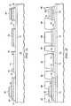
- FIG. 1is a flip chip semiconductor device with solder bumps providing electrical interconnect between an active area of the die and a chip carrier substrate;
- FIGS. 2 a - 2 iillustrate a process of forming an interconnect structure and passive circuit elements
- FIG. 3illustrates an alternate embodiment of the interconnect structure and passive circuit elements
- FIG. 4illustrates another embodiment of the interconnect structure and passive circuit elements
- FIG. 5illustrates another embodiment of the interconnect structure and passive circuit elements.
- Front-end manufacturinggenerally refers to formation of the semiconductor devices on the wafer.
- the finished waferhas an active side containing the transistors and other active and passive components.
- Back-end manufacturingrefers to cutting or singulating the finished wafer into the individual die and then packaging the die for structural support and/or environmental isolation.
- a semiconductor wafergenerally includes an active surface having semiconductor devices disposed thereon, and a backside surface formed with bulk semiconductor material, e.g., silicon.
- the active side surfacecontains a plurality of semiconductor die.
- the active surfaceis formed by a variety of semiconductor processes, including layering, patterning, doping, and heat treatment.
- semiconductor materialsare grown or deposited on the substrate by techniques involving thermal oxidation, nitridation, chemical vapor deposition, evaporation, and sputtering.
- Photolithographyinvolves the masking of areas of the surface and etching away undesired material to form specific structures.
- the doping processinjects concentrations of dopant material by thermal diffusion or ion implantation.
- Flip chip semiconductor packages and wafer level packagesare commonly used with integrated circuits (ICs) demanding high speed, high density, and greater pin count.
- Flip chip style semiconductor device 10involves mounting an active area 12 of die 14 facedown toward a chip carrier substrate or printed circuit board (PCB) 16 , as shown in FIG. 1 .
- Active area 12contains active and passive devices, conductive layers, and dielectric layers according to the electrical design of the die.
- Analog circuitsmay be created by the combination of one or more passive device formed within active area 12 and electrically interconnected.
- an analog circuitmay include one or more inductor, capacitor and resistor formed within active area 12 .
- the electrical and mechanical interconnectis achieved through a solder bump structure 20 comprising a large number of individual conductive solder bumps or balls 22 .
- the solder bumpsare formed on bump pads or interconnect sites 24 , which are disposed on active area 12 .
- the bump pads 24connect to the active circuits by conduction tracks in active area 12 .
- the solder bumps 22are electrically and mechanically connected to contact pads or interconnect sites 26 on carrier substrate 16 by a solder reflow process.
- the flip chip semiconductor deviceprovides a short electrical conduction path from the active devices on die 14 to conduction tracks on carrier substrate 16 in order to reduce signal propagation, lower capacitance, and achieve overall better circuit performance.
- FIG. 2 aillustrates a cross-sectional view of the formation of an interconnect structure and integrated passive devices (IPD) on the substrate.
- a substrate 70is provided which is made of silicon, glass, dielectric, or other bulk semiconductor material.
- a passivation layer 72is deposited over substrate 70 .
- Passivation layer 72can be made with silicon nitride (SixNy), silicon dioxide (SiO2), silicon oxynitride (SiON), polyimide (PI), benzocyclobutene (BCB), polybenzoxazole (PBO), or other insulating material.
- a resistive layer 74is deposited over passivation layer 72 .
- Resistive layer 74is made with a conductive material having relative high resistivity, such as tantalum (Ta) silicide, doped poly-silicon, nickel chromium (NiCr), tantalum nitride (TaN), and titanium nitride (TiN).
- resistive layer 74has a surface resistivity of 5-50 ohm/square.
- the deposition of resistive layer 74may involve physical vapor deposition (PVD) or physical chemical vapor deposition (CVD).
- Conductive layer 76is deposited over resistive layer 74 .
- Conductive layer 76can be made with aluminum (Al), copper (Cu), tin (Sn), nickel (Ni), gold (Au), silver (Ag), or other electrically conductive material.
- Conductive layer 76can made with single or multiple layers, for example with adhesion and barrier layers.
- the adhesion layercan be titanium (Ti), tantalum (Ta), and chromium (Cr).
- the barrier layercan be nickel vanadium (NiV), TiN, and TaN.
- the deposition of conductive layer 76can use an electrolytic plating or electroless plating process, PVD, or CVD.
- a second resistive layer 78is deposited over conductive layer 76 .
- An insulating layer 80is deposited over resistive layer 78 .
- the insulating layer 80is made with Si3N4, SiO2, SiON, tantalum pentoxide (Ta2O5), Zirconium (Zr) oxide, or other dielectric material.
- the deposition of insulating layer 80may involve PVD or CVD with typical thickness of 50 to 4000 angstroms ( ⁇ ).
- An optional electrically conductive layer 82is deposited over insulating layer 80 .
- Conductive layer 82can be made with Al, Cu, Sn, Ni, Au, Ag, or other electrically conductive material.
- Conductive layer 82can be single or multiple layers, for example with adhesion and barrier layers.
- the adhesion layercan be Ti, Ta, or Cr.
- the barrier layercan be NiV, TiN, or TaN.
- the deposition of conductive layer 82uses an electrolytic plating or electroless plating process, PVD, or CVD.
- layers 72 - 82is achieved by patterning and/or deposition of the materials described for each layer.
- the patterning and deposition of layers 72 - 82does not involve any photolithography processes.
- a portion of conductive layer 82is patterned using an etching process, leaving the portion of conductive layer 82 as shown in the FIGS.
- the layers 72 - 82which will make up and constitute analog or passive circuit elements have already been formed by patterning and deposition. Accordingly, layers 72 - 78 have been isolated from particles and other contaminants introduced at the interface of insulating layer 80 and conductive layer 82 in the subsequent photolithographic process.
- portions of resistive layer 78 and insulating layer 80are patterned using an etching process, leaving the portions of resistive layer 78 and insulating layer 80 as shown in the figure.
- a photoresist layeris used as the mask to etch resistive layer 78 and insulating layer 80 .
- conductive layer 82can be used as the mask.
- the portions of resistive layer 78 and insulating layer 80 which remainare typically wider than the remaining portion of conductive layer 82 .
- portions of conductive layer 76are patterned using an etching process, leaving the portions of conductive layer 76 as shown in the figure.
- portions of resistive layer 74are patterned using an etching process, leaving the portions of resistive layer 74 as shown in the figure.
- the photoresist and portions of conductive layer 76are used as the mask for the etching process.
- passivation layer 88is formed over the structure created in FIGS. 2 a - 2 e for structural support and physical isolation.
- Passivation layer 88can be made with SixNy, SiO2, SiON, PI, BCB, PBO, or other insulating material.
- passivation layer 88can be photo-sensitive material. A portion of passivation layer 88 is removed using a wet resist developing process to expose conductive layers 76 and 82 and insulating layer 80 .
- an adhesion layer 90 and electrically conductive layer 92are formed by patterning and deposition as shown.
- Adhesion layer 90can be made with Ti, TiW, Cr, Ta, or TaN.
- Conductive layer 92can be made with Al, Cu, Sn, Ni, Au, Ag, or other electrically conductive material.
- the deposition of conductive layers 90 and 92uses an electrolytic plating or electroless plating process, PVD, or CVD.
- the conductive layer 92can be electrically common or electrically isolated depending on the connectivity of the individual devices formed on substrate 70 .
- a passivation layer 96is formed over the structure created in FIGS. 2 a - 2 g for structural support and physical isolation.
- Passivation layer 96can be made with SixNy, SiO2, SiON, PI, BCB, PBO, or other insulating material.
- passivation layer 96can be photo-sensitive material. A portion of passivation layer 96 is removed using a wet resist developing process to expose conductive layer 92 , which is used in the formation of the solder bump, and insulating layer 80 .
- an electrically conductive solder materialis deposited over conductive layer 92 through an electrolytic plating or electroless plating process, solder paste printing process, or by pre-formed ball mounting process.
- Adhesive layer 90 and conductive layer 92constitute an under bump metallization (UBM) structure.
- UBMunder bump metallization
- additional UBM layersmay be applied under the solder and overlapping the UBM vias.
- the solder materialcan be any metal or electrically conductive material, e.g., Sn, Pb, Ni, Au, Ag, Cu, Bi, Sn/Ag alloy, Sn/Pb alloy.
- the solder materialis reflowed by heating the conductive material above its melting point to form spherical ball or bump 98 . In some applications, solder bump 98 is reflowed a second time to improve electrical contact to the UBM structure.
- insulating layer 80 and resistive layer 78are exposed in openings of passivation layers 88 and 96 either after solder bumps 98 are formed or after patterning of passivation layer 96 .
- Pad 101is used for wire bonding.
- conductive layer 76The combination of conductive layer 76 , resistive layer 78 , insulating layer 80 , and conductive layers 82 , 90 , and 92 constitute an analog or passive circuit, i.e., a metal-insulator-metal (MIM) capacitor with series resistor.
- the passive circuitcan be electrically connected to solder bump 98 and wire bond pad 101 through conductive layers 92 .
- Other examples of an analog or passive circuitinclude an inductor, capacitor, resistor, transmission line, or ground plane.
- the MIM capacitor and resistorare formed layer by layer as described in FIG. 2 a , i.e., using patterning and deposition processes, but without using photolithographic processes.
- the layers constituting the passive circuit elements, including the dielectric media of the MIM capacitor,are sensitive to particles and other contaminants introduced during photolithographic processes such as etching, application of photoresist, wet and dry clean, and wafer handling. These processes are not utilized until the layers of the passive circuit elements are formed and isolated from such contaminants.
- the layer-by-layer continuous deposition for the passive circuit elements in FIG. 2 areduces defects in interfaces between layers, and improves manufacturing yield.
- the photolithographic processes in FIGS. 2 b - 2 ioccur after layer deposition for the passive circuit elements, i.e., the MIM capacitor and resistor layers.
- a portion of conductive layer 76is removed to make direct contact between adhesive layer 90 and conductive layer 92 and resistive layer 74 through vias in passivation layer 88 .
- FIG. 4shows an embodiment of the interconnect structure and IPDs without resistive layer 74 .
- the embodiment in FIG. 4has applications in balun circuits that do not require any resistor component.
- FIG. 5Another embodiment of the formation of IPD and interconnect structure is shown in FIG. 5 .
- the substrate 70 , passivation layer 72 , resistive layer 74 , electrically conductive layer 76 , second resistive layer 78 , and insulating layer 80are formed, as described in FIG. 2 .
- conductive layer 110is deposited and patterned after the deposition and patterning of passivation layer 88 .
- Conductive layer 110also covers wire bonding pad 101 . Note that there is no conductive layer 76 on resistive layer 74 a which is made as a resistor component.
- a passive circuiti.e., an MIM capacitor with series resistor.
- the layers of the passive circuit elementsincluding the dielectric media of the MIM capacitor, are sensitive to particles introduced through masking, application of photoresist, etching, wet and dry clean, and wafer handling steps.
- the layer-by-layer formation of the passive circuit elementsreduces defects and improves manufacturing yield.
- the photolithographic processes in forming the interconnect structure of FIG. 5occur after deposition of multi-layers for formation of the passive circuit elements, i.e., the MIM capacitor and resistor layers.
Landscapes
- Engineering & Computer Science (AREA)
- Power Engineering (AREA)
- Microelectronics & Electronic Packaging (AREA)
- Computer Hardware Design (AREA)
- Manufacturing & Machinery (AREA)
- Physics & Mathematics (AREA)
- Condensed Matter Physics & Semiconductors (AREA)
- General Physics & Mathematics (AREA)
- Semiconductor Integrated Circuits (AREA)
- Internal Circuitry In Semiconductor Integrated Circuit Devices (AREA)
Abstract
Description
Claims (32)
Priority Applications (2)
| Application Number | Priority Date | Filing Date | Title |
|---|---|---|---|
| US11/958,546US8124490B2 (en) | 2006-12-21 | 2007-12-18 | Semiconductor device and method of forming passive devices |
| US13/365,097US9349723B2 (en) | 2006-12-21 | 2012-02-02 | Semiconductor device and method of forming passive devices |
Applications Claiming Priority (2)
| Application Number | Priority Date | Filing Date | Title |
|---|---|---|---|
| US87141606P | 2006-12-21 | 2006-12-21 | |
| US11/958,546US8124490B2 (en) | 2006-12-21 | 2007-12-18 | Semiconductor device and method of forming passive devices |
Related Child Applications (1)
| Application Number | Title | Priority Date | Filing Date |
|---|---|---|---|
| US13/365,097ContinuationUS9349723B2 (en) | 2006-12-21 | 2012-02-02 | Semiconductor device and method of forming passive devices |
Publications (2)
| Publication Number | Publication Date |
|---|---|
| US20080153245A1 US20080153245A1 (en) | 2008-06-26 |
| US8124490B2true US8124490B2 (en) | 2012-02-28 |
Family
ID=46063566
Family Applications (2)
| Application Number | Title | Priority Date | Filing Date |
|---|---|---|---|
| US11/958,546Active2028-09-14US8124490B2 (en) | 2006-12-21 | 2007-12-18 | Semiconductor device and method of forming passive devices |
| US13/365,097ActiveUS9349723B2 (en) | 2006-12-21 | 2012-02-02 | Semiconductor device and method of forming passive devices |
Family Applications After (1)
| Application Number | Title | Priority Date | Filing Date |
|---|---|---|---|
| US13/365,097ActiveUS9349723B2 (en) | 2006-12-21 | 2012-02-02 | Semiconductor device and method of forming passive devices |
Country Status (1)
| Country | Link |
|---|---|
| US (2) | US8124490B2 (en) |
Cited By (4)
| Publication number | Priority date | Publication date | Assignee | Title |
|---|---|---|---|---|
| US20160118301A1 (en)* | 2013-02-11 | 2016-04-28 | Taiwan Semiconductor Manufacturing Co., Ltd. | Package with metal-insulator-metal capacitor and method of manufacturing the same |
| US9991328B2 (en) | 2016-08-25 | 2018-06-05 | International Business Machines Corporation | Tunable on-chip nanosheet resistor |
| US20200058580A1 (en)* | 2018-08-14 | 2020-02-20 | Taiwan Semiconductor Manufacturing Co., Ltd. | Semiconductor structure |
| US11075149B2 (en) | 2019-02-15 | 2021-07-27 | Samsung Electronics Co., Ltd. | Redistribution substrate, method of manufacturing the same, and semiconductor package including the same |
Families Citing this family (26)
| Publication number | Priority date | Publication date | Assignee | Title |
|---|---|---|---|---|
| TWI360207B (en) | 2007-10-22 | 2012-03-11 | Advanced Semiconductor Eng | Chip package structure and method of manufacturing |
| US7951663B2 (en)* | 2009-05-26 | 2011-05-31 | Stats Chippac, Ltd. | Semiconductor device and method of forming IPD structure using smooth conductive layer and bottom-side conductive layer |
| US8164158B2 (en) | 2009-09-11 | 2012-04-24 | Stats Chippac, Ltd. | Semiconductor device and method of forming integrated passive device |
| US8569894B2 (en) | 2010-01-13 | 2013-10-29 | Advanced Semiconductor Engineering, Inc. | Semiconductor package with single sided substrate design and manufacturing methods thereof |
| TWI411075B (en) | 2010-03-22 | 2013-10-01 | Advanced Semiconductor Eng | Semiconductor package and manufacturing method thereof |
| FR2961345A1 (en)* | 2010-06-10 | 2011-12-16 | St Microelectronics Tours Sas | PASSIVE INTEGRATED CIRCUIT |
| US9406658B2 (en) | 2010-12-17 | 2016-08-02 | Advanced Semiconductor Engineering, Inc. | Embedded component device and manufacturing methods thereof |
| IT1403475B1 (en)* | 2010-12-20 | 2013-10-17 | St Microelectronics Srl | CONNECTION STRUCTURE FOR AN INTEGRATED CIRCUIT WITH CAPACITIVE FUNCTION |
| US8552540B2 (en)* | 2011-05-10 | 2013-10-08 | Conexant Systems, Inc. | Wafer level package with thermal pad for higher power dissipation |
| JP2012248814A (en)* | 2011-05-31 | 2012-12-13 | Toshiba Corp | Semiconductor device and manufacturing method of the same |
| US8710658B2 (en) | 2011-11-18 | 2014-04-29 | Cambridge Silicon Radio Limited | Under bump passive components in wafer level packaging |
| US8680647B2 (en)* | 2011-12-29 | 2014-03-25 | Taiwan Semiconductor Manufacturing Company, Ltd. | Packages with passive devices and methods of forming the same |
| US9111949B2 (en) | 2012-04-09 | 2015-08-18 | Taiwan Semiconductor Manufacturing Company, Ltd. | Methods and apparatus of wafer level package for heterogeneous integration technology |
| US8809996B2 (en) | 2012-06-29 | 2014-08-19 | Taiwan Semiconductor Manufacturing Company, Ltd. | Package with passive devices and method of forming the same |
| US9035421B2 (en) | 2013-03-01 | 2015-05-19 | Qualcomm Incorporated | High quality factor inductor implemented in wafer level packaging (WLP) |
| US9373583B2 (en) | 2013-03-01 | 2016-06-21 | Qualcomm Incorporated | High quality factor filter implemented in wafer level packaging (WLP) integrated device |
| US9281355B2 (en) | 2014-05-05 | 2016-03-08 | Texas Instruments Deutschland Gmbh | Integrated thinfilm resistor and MIM capacitor with a low serial resistance |
| CN105575959B (en)* | 2014-11-21 | 2018-06-15 | 威盛电子股份有限公司 | Integrated circuit device |
| US10304765B2 (en) | 2017-06-08 | 2019-05-28 | Advanced Semiconductor Engineering, Inc. | Semiconductor device package |
| US11756948B2 (en)* | 2019-05-01 | 2023-09-12 | Intel Corporation | In situ package integrated thin film capacitors for power delivery |
| US11450733B2 (en) | 2019-07-18 | 2022-09-20 | Taiwan Semiconductor Manufacturing Co., Ltd. | Three dimensional metal insulator metal capacitor structure |
| US11177065B2 (en)* | 2020-03-30 | 2021-11-16 | Qualcomm Incorporated | Thermal paths for glass substrates |
| JP2022006781A (en)* | 2020-06-25 | 2022-01-13 | Tdk株式会社 | Electronic component and method of manufacturing the same |
| US11637100B2 (en) | 2021-08-11 | 2023-04-25 | Globalfoundries Singapore Pte. Ltd. | Semiconductor device having capacitor and resistor and a method of forming the same |
| US11923403B2 (en)* | 2021-08-27 | 2024-03-05 | Taiwan Semiconductor Manufacturing Company, Ltd. | Multi-layered resistor with a tight temperature coefficient of resistance tolerance |
| US12289919B1 (en)* | 2024-04-17 | 2025-04-29 | Globalfoundries Singapore Pte. Ltd. | Buffered top thin film resistor, MIM capacitor, and method of forming the same |
Citations (34)
| Publication number | Priority date | Publication date | Assignee | Title |
|---|---|---|---|---|
| US4963741A (en)* | 1987-06-22 | 1990-10-16 | Molectron Detector, Inc. | Large area pyroelectric joulemeter |
| US6027980A (en)* | 1991-12-31 | 2000-02-22 | Intel Corporation | Method of forming a decoupling capacitor |
| US20010054728A1 (en)* | 1993-12-10 | 2001-12-27 | Symetrix Corporation | Metal oxide integrated circuit on silicon germanium substrate |
| US6448708B1 (en)* | 1997-09-17 | 2002-09-10 | Candescent Intellectual Property Services, Inc. | Dual-layer metal for flat panel display |
| US6452270B1 (en)* | 2000-10-13 | 2002-09-17 | Advanced Semiconductor Engineering, Inc. | Semiconductor device having bump electrode |
| US20020164862A1 (en)* | 1998-12-30 | 2002-11-07 | Lepert Arnaud Yves | Electrostatic discharge protection for sensors |
| US6492222B1 (en)* | 1999-12-22 | 2002-12-10 | Texas Instruments Incorporated | Method of dry etching PZT capacitor stack to form high-density ferroelectric memory devices |
| US6500724B1 (en)* | 2000-08-21 | 2002-12-31 | Motorola, Inc. | Method of making semiconductor device having passive elements including forming capacitor electrode and resistor from same layer of material |
| US20030067053A1 (en)* | 2000-12-15 | 2003-04-10 | Mitsubishi Denki Kabushiki Kaisha | Semiconductor device with capacitor and method of manufacturing thereof |
| US20030080476A1 (en)* | 1998-12-11 | 2003-05-01 | Candescent Technologies Corporation | Constitution and fabrication of flat-panel display and porous-faced structure suitable for partial or full use in spacer of flat-panel display |
| US20040104420A1 (en)* | 2002-12-03 | 2004-06-03 | International Business Machines Corporation | PREVENTION OF Ta2O5 MIM CAP SHORTING IN THE BEOL ANNEAL CYCLES |
| US20040155278A1 (en)* | 2003-02-10 | 2004-08-12 | Katsuaki Natori | Semiconductor device, apparatus and method for manufacturing the same |
| US20040191981A1 (en)* | 2002-04-11 | 2004-09-30 | Yates Donald L. | Methods of fabricating an MRAM device using chemical mechanical polishing |
| US20050017355A1 (en)* | 2003-05-27 | 2005-01-27 | Chien-Kang Chou | Water level processing method and structure to manufacture two kinds of bumps, gold and solder, on one wafer |
| US6919244B1 (en)* | 2004-03-10 | 2005-07-19 | Motorola, Inc. | Method of making a semiconductor device, and semiconductor device made thereby |
| US20050218520A1 (en)* | 2004-03-30 | 2005-10-06 | Nec Electronics Corporation | Semiconductor device and manufacturing method for the same |
| US20050285173A1 (en)* | 2004-06-28 | 2005-12-29 | Fujitsu Limited | Semiconductor device and method for fabricating the same |
| US20060094185A1 (en)* | 2004-01-14 | 2006-05-04 | Samsung Electronics Co., Ltd. | Capacitor including a dielectric layer having an inhomogeneous crystalline region and method of fabricating the same |
| US20060205170A1 (en)* | 2005-03-09 | 2006-09-14 | Rinne Glenn A | Methods of forming self-healing metal-insulator-metal (MIM) structures and related devices |
| US20070059879A1 (en)* | 2005-09-14 | 2007-03-15 | Chin-Kuo Ting | Pixel structure and fabricating method thereof |
| US7214990B1 (en)* | 2003-03-24 | 2007-05-08 | Integrated Device Technology, Inc. | Memory cell with reduced soft error rate |
| US20070114634A1 (en) | 2005-10-29 | 2007-05-24 | Stats Chippac Ltd. | Integrated passive device system |
| US7259077B2 (en) | 2004-04-29 | 2007-08-21 | Sychip Inc. | Integrated passive devices |
| US20070205520A1 (en)* | 2006-03-02 | 2007-09-06 | Megica Corporation | Chip package and method for fabricating the same |
| US20070235878A1 (en) | 2006-03-30 | 2007-10-11 | Stats Chippac Ltd. | Integrated circuit package system with post-passivation interconnection and integration |
| US20080001254A1 (en)* | 2006-06-30 | 2008-01-03 | Fujitsu Limited | Semiconductor device and method of manufacturing the same |
| US20080064179A1 (en)* | 2000-12-20 | 2008-03-13 | Micron Technology, Inc. | Low leakage mim capacitor |
| US7368311B2 (en)* | 2001-04-19 | 2008-05-06 | Interuniversitair Microelektronica Centrum (Imec) | Method and system for fabrication of integrated tunable/switchable passive microwave and millimeter wave modules |
| US20090004809A1 (en)* | 2005-09-12 | 2009-01-01 | International Business Machines Corporation | Method of Integration of a MIM Capacitor with a Lower Plate of Metal Gate Material Formed on an STI Region or a Silicide Region Formed in or on the Surface of a Doped Well with a High K Dielectric Material |
| US7473951B2 (en)* | 2003-09-26 | 2009-01-06 | Samsung Electronics Co., Ltd. | Magnetic random access memory (MRAM) having a magnetic tunneling junction (MTJ) layer including a tunneling film of uniform thickness and method of manufacturing the same |
| US7535079B2 (en)* | 2005-06-09 | 2009-05-19 | Freescale Semiconductor, Inc. | Semiconductor device comprising passive components |
| US7579694B2 (en)* | 2003-02-18 | 2009-08-25 | Unitive International Limited | Electronic devices including offset conductive bumps |
| US7645619B2 (en)* | 2005-02-07 | 2010-01-12 | Samsung Electronics Co., Ltd. | Magnetic random access memory device and method of forming the same |
| US20100218978A1 (en)* | 2003-04-22 | 2010-09-02 | Touchsensor Technologies, Llc | Method of making an electrical circuit |
Family Cites Families (18)
| Publication number | Priority date | Publication date | Assignee | Title |
|---|---|---|---|---|
| US5736448A (en)* | 1995-12-04 | 1998-04-07 | General Electric Company | Fabrication method for thin film capacitors |
| US5874770A (en)* | 1996-10-10 | 1999-02-23 | General Electric Company | Flexible interconnect film including resistor and capacitor layers |
| US7531417B2 (en)* | 1998-12-21 | 2009-05-12 | Megica Corporation | High performance system-on-chip passive device using post passivation process |
| WO2000049660A1 (en)* | 1999-02-16 | 2000-08-24 | Symetrix Corporation | Iridium oxide diffusion barrier between local interconnect layer and thin film of layered superlattice material |
| JP3745553B2 (en)* | 1999-03-04 | 2006-02-15 | 富士通株式会社 | Ferroelectric capacitor and method for manufacturing semiconductor device |
| US6838717B1 (en)* | 2000-08-31 | 2005-01-04 | Agere Systems Inc. | Stacked structure for parallel capacitors and method of fabrication |
| US6365480B1 (en)* | 2000-11-27 | 2002-04-02 | Analog Devices, Inc. | IC resistor and capacitor fabrication method |
| JP4947849B2 (en)* | 2001-05-30 | 2012-06-06 | ルネサスエレクトロニクス株式会社 | Semiconductor device and manufacturing method thereof |
| TWI240352B (en)* | 2001-08-03 | 2005-09-21 | Winbond Electronics Corp | Integrated circuit device of high Q MIM capacitor and manufacturing process thereof |
| US6902981B2 (en)* | 2002-10-10 | 2005-06-07 | Chartered Semiconductor Manufacturing Ltd | Structure and process for a capacitor and other devices |
| TWI236763B (en)* | 2003-05-27 | 2005-07-21 | Megic Corp | High performance system-on-chip inductor using post passivation process |
| US6777777B1 (en)* | 2003-05-28 | 2004-08-17 | Newport Fab, Llc | High density composite MIM capacitor with flexible routing in semiconductor dies |
| US7470997B2 (en)* | 2003-07-23 | 2008-12-30 | Megica Corporation | Wirebond pad for semiconductor chip or wafer |
| US7056800B2 (en)* | 2003-12-15 | 2006-06-06 | Motorola, Inc. | Printed circuit embedded capacitors |
| JP4308691B2 (en)* | 2004-03-19 | 2009-08-05 | 富士通マイクロエレクトロニクス株式会社 | Semiconductor substrate and method for manufacturing semiconductor substrate |
| KR101184013B1 (en)* | 2006-09-27 | 2012-09-18 | 후지쯔 세미컨덕터 가부시키가이샤 | Semiconductor device having capacitor and its manufacturing method |
| US7727879B2 (en)* | 2007-03-21 | 2010-06-01 | Stats Chippac, Ltd. | Method of forming top electrode for capacitor and interconnection in integrated passive device (IPD) |
| US7863706B2 (en)* | 2007-06-28 | 2011-01-04 | Stats Chippac Ltd. | Circuit system with circuit element |
- 2007
- 2007-12-18USUS11/958,546patent/US8124490B2/enactiveActive
- 2012
- 2012-02-02USUS13/365,097patent/US9349723B2/enactiveActive
Patent Citations (35)
| Publication number | Priority date | Publication date | Assignee | Title |
|---|---|---|---|---|
| US4963741A (en)* | 1987-06-22 | 1990-10-16 | Molectron Detector, Inc. | Large area pyroelectric joulemeter |
| US6027980A (en)* | 1991-12-31 | 2000-02-22 | Intel Corporation | Method of forming a decoupling capacitor |
| US20010054728A1 (en)* | 1993-12-10 | 2001-12-27 | Symetrix Corporation | Metal oxide integrated circuit on silicon germanium substrate |
| US6448708B1 (en)* | 1997-09-17 | 2002-09-10 | Candescent Intellectual Property Services, Inc. | Dual-layer metal for flat panel display |
| US20030080476A1 (en)* | 1998-12-11 | 2003-05-01 | Candescent Technologies Corporation | Constitution and fabrication of flat-panel display and porous-faced structure suitable for partial or full use in spacer of flat-panel display |
| US20020164862A1 (en)* | 1998-12-30 | 2002-11-07 | Lepert Arnaud Yves | Electrostatic discharge protection for sensors |
| US6492222B1 (en)* | 1999-12-22 | 2002-12-10 | Texas Instruments Incorporated | Method of dry etching PZT capacitor stack to form high-density ferroelectric memory devices |
| US6500724B1 (en)* | 2000-08-21 | 2002-12-31 | Motorola, Inc. | Method of making semiconductor device having passive elements including forming capacitor electrode and resistor from same layer of material |
| US6452270B1 (en)* | 2000-10-13 | 2002-09-17 | Advanced Semiconductor Engineering, Inc. | Semiconductor device having bump electrode |
| US20030067053A1 (en)* | 2000-12-15 | 2003-04-10 | Mitsubishi Denki Kabushiki Kaisha | Semiconductor device with capacitor and method of manufacturing thereof |
| US20080064179A1 (en)* | 2000-12-20 | 2008-03-13 | Micron Technology, Inc. | Low leakage mim capacitor |
| US7368311B2 (en)* | 2001-04-19 | 2008-05-06 | Interuniversitair Microelektronica Centrum (Imec) | Method and system for fabrication of integrated tunable/switchable passive microwave and millimeter wave modules |
| US20040191981A1 (en)* | 2002-04-11 | 2004-09-30 | Yates Donald L. | Methods of fabricating an MRAM device using chemical mechanical polishing |
| US20040104420A1 (en)* | 2002-12-03 | 2004-06-03 | International Business Machines Corporation | PREVENTION OF Ta2O5 MIM CAP SHORTING IN THE BEOL ANNEAL CYCLES |
| US20040155278A1 (en)* | 2003-02-10 | 2004-08-12 | Katsuaki Natori | Semiconductor device, apparatus and method for manufacturing the same |
| US7579694B2 (en)* | 2003-02-18 | 2009-08-25 | Unitive International Limited | Electronic devices including offset conductive bumps |
| US7214990B1 (en)* | 2003-03-24 | 2007-05-08 | Integrated Device Technology, Inc. | Memory cell with reduced soft error rate |
| US20100218978A1 (en)* | 2003-04-22 | 2010-09-02 | Touchsensor Technologies, Llc | Method of making an electrical circuit |
| US20050017355A1 (en)* | 2003-05-27 | 2005-01-27 | Chien-Kang Chou | Water level processing method and structure to manufacture two kinds of bumps, gold and solder, on one wafer |
| US7473951B2 (en)* | 2003-09-26 | 2009-01-06 | Samsung Electronics Co., Ltd. | Magnetic random access memory (MRAM) having a magnetic tunneling junction (MTJ) layer including a tunneling film of uniform thickness and method of manufacturing the same |
| US20060094185A1 (en)* | 2004-01-14 | 2006-05-04 | Samsung Electronics Co., Ltd. | Capacitor including a dielectric layer having an inhomogeneous crystalline region and method of fabricating the same |
| US6919244B1 (en)* | 2004-03-10 | 2005-07-19 | Motorola, Inc. | Method of making a semiconductor device, and semiconductor device made thereby |
| US20050218520A1 (en)* | 2004-03-30 | 2005-10-06 | Nec Electronics Corporation | Semiconductor device and manufacturing method for the same |
| US20070148825A1 (en)* | 2004-03-30 | 2007-06-28 | Nec Electronics Corporation | Semiconductor device and manufacturing method for the same |
| US7259077B2 (en) | 2004-04-29 | 2007-08-21 | Sychip Inc. | Integrated passive devices |
| US20050285173A1 (en)* | 2004-06-28 | 2005-12-29 | Fujitsu Limited | Semiconductor device and method for fabricating the same |
| US7645619B2 (en)* | 2005-02-07 | 2010-01-12 | Samsung Electronics Co., Ltd. | Magnetic random access memory device and method of forming the same |
| US20060205170A1 (en)* | 2005-03-09 | 2006-09-14 | Rinne Glenn A | Methods of forming self-healing metal-insulator-metal (MIM) structures and related devices |
| US7535079B2 (en)* | 2005-06-09 | 2009-05-19 | Freescale Semiconductor, Inc. | Semiconductor device comprising passive components |
| US20090004809A1 (en)* | 2005-09-12 | 2009-01-01 | International Business Machines Corporation | Method of Integration of a MIM Capacitor with a Lower Plate of Metal Gate Material Formed on an STI Region or a Silicide Region Formed in or on the Surface of a Doped Well with a High K Dielectric Material |
| US20070059879A1 (en)* | 2005-09-14 | 2007-03-15 | Chin-Kuo Ting | Pixel structure and fabricating method thereof |
| US20070114634A1 (en) | 2005-10-29 | 2007-05-24 | Stats Chippac Ltd. | Integrated passive device system |
| US20070205520A1 (en)* | 2006-03-02 | 2007-09-06 | Megica Corporation | Chip package and method for fabricating the same |
| US20070235878A1 (en) | 2006-03-30 | 2007-10-11 | Stats Chippac Ltd. | Integrated circuit package system with post-passivation interconnection and integration |
| US20080001254A1 (en)* | 2006-06-30 | 2008-01-03 | Fujitsu Limited | Semiconductor device and method of manufacturing the same |
Cited By (9)
| Publication number | Priority date | Publication date | Assignee | Title |
|---|---|---|---|---|
| US20160118301A1 (en)* | 2013-02-11 | 2016-04-28 | Taiwan Semiconductor Manufacturing Co., Ltd. | Package with metal-insulator-metal capacitor and method of manufacturing the same |
| US10153205B2 (en)* | 2013-02-11 | 2018-12-11 | Taiwan Semiconductor Manufacturing Co., Ltd. | Package with metal-insulator-metal capacitor and method of manufacturing the same |
| US9991328B2 (en) | 2016-08-25 | 2018-06-05 | International Business Machines Corporation | Tunable on-chip nanosheet resistor |
| US10586843B2 (en) | 2016-08-25 | 2020-03-10 | International Business Machines Corporation | Tunable on-chip nanosheet resistor |
| US10985236B2 (en) | 2016-08-25 | 2021-04-20 | International Business Machines Corporation | Tunable on-chip nanosheet resistor |
| US20200058580A1 (en)* | 2018-08-14 | 2020-02-20 | Taiwan Semiconductor Manufacturing Co., Ltd. | Semiconductor structure |
| US10879172B2 (en)* | 2018-08-14 | 2020-12-29 | Taiwan Semiconductor Manufacturing Co., Ltd. | Semiconductor structure |
| US11075149B2 (en) | 2019-02-15 | 2021-07-27 | Samsung Electronics Co., Ltd. | Redistribution substrate, method of manufacturing the same, and semiconductor package including the same |
| US11626354B2 (en) | 2019-02-15 | 2023-04-11 | Samsung Electronics Co., Ltd. | Method of manufacturing redistribution substrate |
Also Published As
| Publication number | Publication date |
|---|---|
| US9349723B2 (en) | 2016-05-24 |
| US20120126369A1 (en) | 2012-05-24 |
| US20080153245A1 (en) | 2008-06-26 |
Similar Documents
| Publication | Publication Date | Title |
|---|---|---|
| US8124490B2 (en) | Semiconductor device and method of forming passive devices | |
| US8039960B2 (en) | Solder bump with inner core pillar in semiconductor package | |
| US10276484B2 (en) | Package with metal-insulator-metal capacitor and method of manufacturing the same | |
| US7749814B2 (en) | Semiconductor device with integrated passive circuit and method of making the same using sacrificial substrate | |
| US7727876B2 (en) | Semiconductor device and method of protecting passivation layer in a solder bump process | |
| US8592311B2 (en) | Semiconductor device and method for forming passive circuit elements with through silicon vias to backside interconnect structures | |
| US7772106B2 (en) | Method of forming an inductor on a semiconductor wafer | |
| US9449925B2 (en) | Integrated passive devices | |
| US7667335B2 (en) | Semiconductor package with passivation island for reducing stress on solder bumps | |
| US20140159236A1 (en) | Semiconductor Device Having High-Density Interconnect Array with Core Pillars Formed With OSP Coating | |
| US20090140441A1 (en) | Wafer Level Die Integration and Method | |
| US20090146282A1 (en) | Semiconductor Package and Method of Forming Similar Structure for Top and Bottom Bonding Pads | |
| US7176117B2 (en) | Method for mounting passive components on wafer | |
| US9466577B2 (en) | Semiconductor interconnect structure with stacked vias separated by signal line and method therefor |
Legal Events
| Date | Code | Title | Description |
|---|---|---|---|
| AS | Assignment | Owner name:STATS CHIPPAC, LTD., SINGAPORE Free format text:ASSIGNMENT OF ASSIGNORS INTEREST;ASSIGNORS:LIN, YAOJIAN;CAO, HAIJING;ZHANG, QING;AND OTHERS;REEL/FRAME:020262/0129;SIGNING DATES FROM 20071129 TO 20071218 Owner name:STATS CHIPPAC, LTD., SINGAPORE Free format text:ASSIGNMENT OF ASSIGNORS INTEREST;ASSIGNORS:LIN, YAOJIAN;CAO, HAIJING;ZHANG, QING;AND OTHERS;SIGNING DATES FROM 20071129 TO 20071218;REEL/FRAME:020262/0129 | |
| STCF | Information on status: patent grant | Free format text:PATENTED CASE | |
| AS | Assignment | Owner name:CITICORP INTERNATIONAL LIMITED, AS COMMON SECURITY AGENT, HONG KONG Free format text:SECURITY INTEREST;ASSIGNORS:STATS CHIPPAC, INC.;STATS CHIPPAC LTD.;REEL/FRAME:036288/0748 Effective date:20150806 Owner name:CITICORP INTERNATIONAL LIMITED, AS COMMON SECURITY Free format text:SECURITY INTEREST;ASSIGNORS:STATS CHIPPAC, INC.;STATS CHIPPAC LTD.;REEL/FRAME:036288/0748 Effective date:20150806 | |
| FPAY | Fee payment | Year of fee payment:4 | |
| AS | Assignment | Owner name:STATS CHIPPAC PTE. LTE., SINGAPORE Free format text:CHANGE OF NAME;ASSIGNOR:STATS CHIPPAC LTD.;REEL/FRAME:038378/0280 Effective date:20160329 | |
| MAFP | Maintenance fee payment | Free format text:PAYMENT OF MAINTENANCE FEE, 8TH YEAR, LARGE ENTITY (ORIGINAL EVENT CODE: M1552); ENTITY STATUS OF PATENT OWNER: LARGE ENTITY Year of fee payment:8 | |
| AS | Assignment | Owner name:STATS CHIPPAC PTE. LTD. FORMERLY KNOWN AS STATS CHIPPAC LTD., SINGAPORE Free format text:RELEASE BY SECURED PARTY;ASSIGNOR:CITICORP INTERNATIONAL LIMITED, AS COMMON SECURITY AGENT;REEL/FRAME:052879/0852 Effective date:20190503 Owner name:STATS CHIPPAC, INC., CALIFORNIA Free format text:RELEASE BY SECURED PARTY;ASSIGNOR:CITICORP INTERNATIONAL LIMITED, AS COMMON SECURITY AGENT;REEL/FRAME:052879/0852 Effective date:20190503 | |
| MAFP | Maintenance fee payment | Free format text:PAYMENT OF MAINTENANCE FEE, 12TH YEAR, LARGE ENTITY (ORIGINAL EVENT CODE: M1553); ENTITY STATUS OF PATENT OWNER: LARGE ENTITY Year of fee payment:12 | |
| AS | Assignment | Owner name:STATS CHIPPAC PTE. LTE., SINGAPORE Free format text:CORRECT ERROR IN ASSIGNMENT NAME FROM STATS CHIPPAC PTE. LTE. TO STATS CHIPPAC PTE. LTD. (REEL: 38378 FRAME: 0280);ASSIGNOR:STATS CHIPPAC LTD.;REEL/FRAME:064789/0474 Effective date:20160329 | |
| AS | Assignment | Owner name:STATS CHIPPAC PTE. LTD., SINGAPORE Free format text:CORRECTIVE ASSIGNMENT TO CORRECT THE RECEIVING PARTY NAME PREVIOUSLY RECORDED AT REEL: 064789 FRAME: 0474 ASSIGNOR(S) HEREBY CONFIRMS THE CHANGE OF NAME;ASSIGNOR:STATS CHIPPAC LTD.;REEL/FRAME:064842/0046 Effective date:20160329 |