US8122207B2 - Apparatus and method for power management of memory circuits by a system or component thereof - Google Patents
Apparatus and method for power management of memory circuits by a system or component thereofDownload PDFInfo
- Publication number
- US8122207B2 US8122207B2US12/816,756US81675610AUS8122207B2US 8122207 B2US8122207 B2US 8122207B2US 81675610 AUS81675610 AUS 81675610AUS 8122207 B2US8122207 B2US 8122207B2
- Authority
- US
- United States
- Prior art keywords
- memory
- address
- circuit
- circuits
- bus
- Prior art date
- Legal status (The legal status is an assumption and is not a legal conclusion. Google has not performed a legal analysis and makes no representation as to the accuracy of the status listed.)
- Active
Links
Images


Classifications
- G—PHYSICS
- G06—COMPUTING OR CALCULATING; COUNTING
- G06F—ELECTRIC DIGITAL DATA PROCESSING
- G06F30/00—Computer-aided design [CAD]
- G06F30/20—Design optimisation, verification or simulation
- G—PHYSICS
- G11—INFORMATION STORAGE
- G11C—STATIC STORES
- G11C11/00—Digital stores characterised by the use of particular electric or magnetic storage elements; Storage elements therefor
- G11C11/21—Digital stores characterised by the use of particular electric or magnetic storage elements; Storage elements therefor using electric elements
- G11C11/34—Digital stores characterised by the use of particular electric or magnetic storage elements; Storage elements therefor using electric elements using semiconductor devices
- G11C11/40—Digital stores characterised by the use of particular electric or magnetic storage elements; Storage elements therefor using electric elements using semiconductor devices using transistors
- G11C11/401—Digital stores characterised by the use of particular electric or magnetic storage elements; Storage elements therefor using electric elements using semiconductor devices using transistors forming cells needing refreshing or charge regeneration, i.e. dynamic cells
- G11C11/4063—Auxiliary circuits, e.g. for addressing, decoding, driving, writing, sensing or timing
- G11C11/407—Auxiliary circuits, e.g. for addressing, decoding, driving, writing, sensing or timing for memory cells of the field-effect type
- G11C11/4074—Power supply or voltage generation circuits, e.g. bias voltage generators, substrate voltage generators, back-up power, power control circuits
- G—PHYSICS
- G11—INFORMATION STORAGE
- G11C—STATIC STORES
- G11C11/00—Digital stores characterised by the use of particular electric or magnetic storage elements; Storage elements therefor
- G11C11/21—Digital stores characterised by the use of particular electric or magnetic storage elements; Storage elements therefor using electric elements
- G11C11/34—Digital stores characterised by the use of particular electric or magnetic storage elements; Storage elements therefor using electric elements using semiconductor devices
- G11C11/40—Digital stores characterised by the use of particular electric or magnetic storage elements; Storage elements therefor using electric elements using semiconductor devices using transistors
- G11C11/401—Digital stores characterised by the use of particular electric or magnetic storage elements; Storage elements therefor using electric elements using semiconductor devices using transistors forming cells needing refreshing or charge regeneration, i.e. dynamic cells
- G11C11/4063—Auxiliary circuits, e.g. for addressing, decoding, driving, writing, sensing or timing
- G11C11/407—Auxiliary circuits, e.g. for addressing, decoding, driving, writing, sensing or timing for memory cells of the field-effect type
- G11C11/409—Read-write [R-W] circuits
- G11C11/4093—Input/output [I/O] data interface arrangements, e.g. data buffers
- G—PHYSICS
- G11—INFORMATION STORAGE
- G11C—STATIC STORES
- G11C5/00—Details of stores covered by group G11C11/00
- G11C5/14—Power supply arrangements, e.g. power down, chip selection or deselection, layout of wirings or power grids, or multiple supply levels
Definitions
- the present inventionrelates to memory, and more particularly to power management in memory systems that contain multiple memory circuits.
- An apparatus and methodare provided for communicating with a plurality of physical memory circuits.
- at least one virtual memory circuitis simulated where at least one aspect (e.g. power-related aspect, etc.) of such virtual memory circuit(s) is different from at least one aspect of at least one of the physical memory circuits. Further, in various embodiments, such simulation may be carried out by a system (or component thereof), an interface circuit, etc.
- FIG. 1illustrates a multiple memory circuit framework, in accordance with one embodiment.
- FIG. 2shows an exemplary embodiment of an interface circuit including a register and a buffer that is operable to interface memory circuits and a system.
- FIG. 3shows an alternative exemplary embodiment of an interface circuit including a register and a buffer that is operable to interface memory circuits and a system.
- FIG. 4shows an exemplary embodiment of an interface circuit including an advanced memory buffer (AMB) and a buffer that is operable to interface memory circuits and a system.
- AMBadvanced memory buffer
- FIG. 5shows an exemplary embodiment of an interface circuit including an AMB, a register, and a buffer that is operable to interface memory circuits and a system.
- FIG. 6shows an alternative exemplary embodiment of an interface circuit including an AMB and a buffer that is operable to interface memory circuits and a system.
- FIG. 7shows an exemplary embodiment of a plurality of physical memory circuits that are mapped by a system, and optionally an interface circuit, to appear as a virtual memory circuit with one aspect that is different from that of the physical memory circuits.
- FIG. 8illustrates an embodiment of a multiple memory circuit framework.
- FIG. 9shows an exemplary embodiment of an interface circuit that is operable to interface memory circuits and a system.
- FIG. 10is a flowchart showing an embodiment of a method for simulating at least one virtual memory circuit.
- FIG. 1illustrates a multiple memory circuit framework 100 , in accordance with one embodiment. As shown, included are an interface circuit 102 , a plurality of memory circuits 104 A, 104 B, 104 N, and a system 106 . In the context of the present description, such memory circuits 104 A, 104 B, 104 N may include any circuit capable of serving as memory.
- At least one of the memory circuits 104 A, 104 B, 104 Nmay include a monolithic memory circuit, a semiconductor die, a chip, a packaged memory circuit, or any other type of tangible memory circuit.
- the memory circuits 104 A, 104 B, 104 Nmay take the form of a dynamic random access memory (DRAM) circuit.
- DRAMdynamic random access memory
- Such DRAMmay take any form including, but not limited to, synchronous DRAM (SDRAM), double data rate synchronous DRAM (DDR SDRAM, DDR2 SDRAM, DDR3 SDRAM, etc.), graphics double data rate synchronous DRAM (GDDR SDRAM, GDDR2 SDRAM, GDDR3 SDRAM, etc.), quad data rate DRAM (QDR DRAM), RAMBUS XDR DRAM (SDR DRAM), fast page mode DRAM (FPM DRAM), video DRAM (VDRAM), extended data out DRAM (EDO DRAM), burst EDO RAM (BEDO DRAM), multibank DRAM (MDRAM), synchronous graphics RAM (SGRAM), and/or any other type of DRAM.
- SDRAMsynchronous DRAM
- DDR SDRAMdouble data rate synchronous DRAM
- DDR2 SDRAMDDR2 SDRAM
- DDR3 SDRAMgraphics double data rate synchronous DRAM
- QDR DRAMquad data rate DRAM
- SDR DRAMRAMBUS XDR DRAM
- FPM DRAMfast
- At least one of the memory circuits 104 A, 104 B, 104 Nmay include magnetic random access memory (MRAM), intelligent random access memory (IRAM), distributed network architecture (DNA) memory, window random access memory (WRAM), flash memory (e.g.
- MRAMmagnetic random access memory
- IRAMintelligent random access memory
- DNAdistributed network architecture
- WRAMwindow random access memory
- flash memorye.g.
- NANDNAND, NOR, etc.
- pseudostatic random access memoryPSRAM
- LP-SDRAMLow-Power Synchronous Dynamic Random Access Memory
- PFRAMPolymer Ferroelectric RAM
- OFUMOVONICS Unified Memory
- PCMPhase-change Memory
- PRAMPhase-change Random Access Memory
- FeRAMFerrolectric RAM
- R-RAM or RRAMREsistance RAM
- wetware memorymemory based on semiconductor, atomic, molecular, optical, organic, biological, chemical, or nanoscale technology, and/or any other type of volatile or nonvolatile, random or non-random access, serial or parallel access memory circuit.
- the memory circuits 104 A, 104 B, 104 Nmay or may not be positioned on at least one dual in-line memory module (DIMM) (not shown).
- the DIMMmay include a registered DIMM (R-DIMM), a small outline-DIMM (SO-DIMM), a fully buffered DIMM (FB-DIMM), an unbuffered DIMM (UDIMM), single inline memory module (SIMM), a MiniDIMM, a very low profile (VLP) R-DIMM, etc.
- the memory circuits 104 A, 104 B, 104 Nmay or may not be positioned on any type of material forming a substrate, card, module, sheet, fabric, board, carrier or other any other type of solid or flexible entity, form, or object.
- the memory circuits 104 A, 104 B, 104 Nmay or may not be positioned in or on any desired entity, form, or object for packaging purposes.
- the memory circuits 104 A, 104 B, 104 Nmay or may not be organized, either as a group (or as groups) collectively, or individually, onto one or more portions(s).
- the term portion(s)e.g.
- a memory circuit(s)shall refer to any physical, logical or electrical arrangement(s), partition(s), subdivisions(s) (e.g. banks, sub-banks, ranks, sub-ranks, rows, columns, pages, etc.), or any other portion(s), for that matter.
- the system 106may include any system capable of requesting and/or initiating a process that results in an access of the memory circuits 104 A, 104 B, 104 N. As an option, the system 106 may accomplish this utilizing a memory controller (not shown), or any other desired mechanism.
- a memory controllernot shown
- such system 106may include a system in the form of a desktop computer, a lap-top computer, a server, a storage system, a networking system, a workstation, a personal digital assistant (PDA), a mobile phone, a television, a computer peripheral (e.g. printer, etc.), a consumer electronics system, a communication system, and/or any other software and/or hardware, for that matter.
- PDApersonal digital assistant
- the interface circuit 102may, in the context of the present description, refer to any circuit capable of communicating (e.g. interfacing, buffering, etc.) with the memory circuits 104 A, 104 B, 104 N and the system 106 .
- the interface circuit 102may, in the context of different embodiments, include a circuit capable of directly (e.g. via wire, bus, connector, and/or any other direct communication medium, etc.) and/or indirectly (e.g. via wireless, optical, capacitive, electric field, magnetic field, electromagnetic field, and/or any other indirect communication medium, etc.) communicating with the memory circuits 104 A, 104 B, 104 N and the system 106 .
- the communicationmay use a direct connection (e.g.
- point-to-pointsingle-drop bus, multi-drop bus, serial bus, parallel bus, link, and/or any other direct connection, etc.
- indirect connectione.g. through intermediate circuits, intermediate logic, an intermediate bus or busses, and/or any other indirect connection, etc.
- the interface circuit 102may include one or more circuits, such as a buffer (e.g. buffer chip, multiplexer/de-multiplexer chip, synchronous multiplexer/de-multiplexer chip, etc.), register (e.g. register chip, data register chip, address/control register chip, etc.), advanced memory buffer (AMB) (e.g. AMB chip, etc.), a component positioned on at least one DIMM, etc.
- a buffere.g. buffer chip, multiplexer/de-multiplexer chip, synchronous multiplexer/de-multiplexer chip, etc.
- registere.g. register chip, data register chip, address/control register chip, etc.
- AMBadvanced memory buffer
- a component positioned on at least one DIMMetc.
- a buffer chipmay be used to interface bidirectional data signals, and may or may not use a clock to re-time or re-synchronize signals in a well known manner.
- a bidirectional signalis a well known use of a single connection to transmit data in two directions.
- a data register chipmay be a register chip that also interfaces bidirectional data signals.
- a multiplexer/de-multiplexer chipis a well known circuit that may interface a first number of bidirectional signals to a second number of bidirectional signals.
- a synchronous multiplexer/de-multiplexer chipmay additionally use a clock to re-time or re-synchronize the first or second number of signals.
- a register chipmay be used to interface and optionally re-time or re-synchronize address and control signals.
- address/control register chipmay be used to distinguish a register chip that only interfaces address and control signals from a data register chip, which may also interface data signals.
- the registermay, in various embodiments, include a JEDEC Solid State Technology Association (known as JEDEC) standard register (a JEDEC register), a register with forwarding, storing, and/or buffering capabilities, etc.
- JEDECJoint State Technology Association
- the registers, buffers, and/or any other interface circuit(s) 102may be intelligent, that is, include logic that are capable of one or more functions such as gathering and/or storing information; inferring, predicting, and/or storing state and/or status; performing logical decisions; and/or performing operations on input signals, etc.
- the interface circuit 102may optionally be manufactured in monolithic form, packaged form, printed form, and/or any other manufactured form of circuit, for that matter.
- a plurality of the aforementioned interface circuits 102may serve, in combination, to interface the memory circuits 104 A, 104 B, 104 N and the system 106 .
- one, two, three, four, or more interface circuits 102may be utilized for such interfacing purposes.
- multiple interface circuits 102may be relatively configured or connected in any desired manner.
- the interface circuits 102may be configured or connected in parallel, serially, or in various combinations thereof.
- the multiple interface circuits 102may use direct connections to each other, indirect connections to each other, or even a combination thereof.
- any number of the interface circuits 102may be allocated to any number of the memory circuits 104 A, 104 B, 104 N.
- each of the plurality of interface circuits 102may be the same or different. Even still, the interface circuits 102 may share the same or similar interface tasks and/or perform different interface tasks.
- memory circuits 104 A, 104 B, 104 N, interface circuit 102 , and system 106are shown to be separate parts, it is contemplated that any of such parts (or portion(s) thereof) may be integrated in any desired manner. In various embodiments, such optional integration may involve simply packaging such parts together (e.g. stacking the parts to form a stack of DRAM circuits, a DRAM stack, a plurality of DRAM stacks, a hardware stack, where a stack may refer to any bundle, collection, or grouping of parts and/or circuits, etc.) and/or integrating them monolithically.
- At least one interface circuit 102may be packaged with at least one of the memory circuits 104 A, 104 B, 104 N.
- a DRAM stackmay or may not include at least one interface circuit (or portion(s) thereof).
- different numbers of the interface circuit 102 (or portions(s) thereof)may be packaged together. Such different packaging arrangements, when employed, may optionally improve the utilization of a monolithic silicon implementation, for example.
- the interface circuit 102may be capable of various functionality, in the context of different embodiments.
- the interface circuit 102may interface a plurality of signals 108 that are connected between the memory circuits 104 A, 104 B, 104 N and the system 106 .
- the signals 108may, for example, include address signals, data signals, control signals, enable signals, clock signals, reset signals, or any other signal used to operate or associated with the memory circuits, system, or interface circuit(s), etc.
- the signalsmay be those that: use a direct connection, use an indirect connection, use a dedicated connection, may be encoded across several connections, and/or may be otherwise encoded (e.g. time-multiplexed, etc.) across one or more connections.
- the interfaced signals 108may represent all of the signals that are connected between the memory circuits 104 A, 104 B, 104 N and the system 106 .
- signals 110may use direct connections between the memory circuits 104 A, 104 B, 104 N and the system 106 .
- the signals 110may, for example, include address signals, data signals, control signals, enable signals, clock signals, reset signals, or any other signal used to operate or associated with the memory circuits, system, or interface circuit(s), etc.
- the signalsmay be those that: use a direct connection, use an indirect connection, use a dedicated connection, may be encoded across several connections, and/or may be otherwise encoded (e.g.
- the number of interfaced signals 108may vary such that the interfaced signals 108 may include at least a majority of the total number of signal connections between the memory circuits 104 A, 104 B, 104 N and the systems 106 (e.g. L>M, with L and M as shown in FIG. 1 ). In other embodiments, L may be less than or equal to M. In still other embodiments L and/or M may be zero.
- the interface circuit 102 and/or any component of the system 106may or may not be operable to communicate with the memory circuits 104 A, 104 B, 104 N for simulating at least one memory circuit.
- the memory circuits 104 A, 104 B, 104 Nshall hereafter be referred to, where appropriate for clarification purposes, as the “physical” memory circuits or memory circuits, but are not limited to be so.
- the physical memory circuitsmay include a single physical memory circuit.
- the at least one simulated memory circuitshall hereafter be referred to, where appropriate for clarification purposes, as the at least one “virtual” memory circuit.
- any property or aspect of such a physical memory circuitshall be referred to, where appropriate for clarification purposes, as a physical aspect (e.g. physical bank, physical portion, physical timing parameter, etc.).
- a physical aspecte.g. physical bank, physical portion, physical timing parameter, etc.
- a virtual aspecte.g. virtual bank, virtual portion, virtual timing parameter, etc.
- the term simulate or simulationmay refer to any simulating, emulating, transforming, disguising modifying, changing, altering, shaping, converting, etc., of at least one aspect of the memory circuits.
- such aspectmay include, for example, a number, a signal, a capacity, a portion (e.g. bank, partition, etc.), an organization (e.g. bank organization, etc.), a mapping (e.g. address mapping, etc.), a timing, a latency, a design parameter, a logical interface, a control system, a property, a behavior, and/or any other aspect, for that matter.
- any of the previous aspects or any other aspect, for that mattermay be power-related, meaning that such power-related aspect, at least in part, directly or indirectly affects power.
- the simulationmay be electrical in nature, logical in nature, protocol in nature, and/or performed in any other desired manner. For instance, in the context of electrical simulation, a number of pins, wires, signals, etc. may be simulated. In the context of logical simulation, a particular function or behavior may be simulated. In the context of protocol, a particular protocol (e.g. DDR3, etc.) may be simulated. Further, in the context of protocol, the simulation may effect conversion between different protocols (e.g. DDR2 and DDR3) or may effect conversion between different versions of the same protocol (e.g. conversion of 4-4-4 DDR2 to 6-6-6 DDR2).
- the aforementioned virtual aspectmay be simulated (e.g. simulate a virtual aspect, the simulation of a virtual aspect, a simulated virtual aspect etc.).
- map, mapping, mapped, etc.refer to the link or connection from the physical aspects to the virtual aspects (e.g. map a physical aspect to a virtual aspect, mapping a physical aspect to a virtual aspect, a physical aspect mapped to a virtual aspect etc.). It should be noted that any use of such mapping or anything equivalent thereto is deemed to fall within the scope of the previously defined simulate or simulation term.
- FIG. 2shows an exemplary embodiment of an interface circuit that is operable to interface memory circuits 202 A-D and a system 204 .
- the interface circuitincludes a register 206 and a buffer 208 .
- Address and control signals 220 from the system 204are connected to the register 206
- data signals 230 from the system 204are connected to the buffer 208 .
- the register 206drives address and control signals 240 to the memory circuits 202 A-D and optionally drives address and control signals 250 to the buffer 208 .
- Data signals 260 of the memory circuits 202 A-Dare connected to the buffer 208 .
- FIG. 3shows an exemplary embodiment of an interface circuit that is operable to interface memory circuits 302 A-D and a system 304 .
- the interface circuitincludes a register 306 and a buffer 308 .
- Address and control signals 320 from the system 304are connected to the register 306
- data signals 330 from the system 304are connected to the buffer 308 .
- the register 306drives address and control signals 340 to the buffer 308 , and optionally drives control signals 350 to the memory circuits 302 A-D.
- the buffer 308drives address and control signals 360 .
- Data signals 370 of the memory circuits 304 A-Dare connected to the buffer 308 .
- FIG. 4shows an exemplary embodiment of an interface circuit that is operable to interface memory circuits 402 A-D and a system 404 .
- the interface circuitincludes an advanced memory buffer (AMB) 406 and a buffer 408 .
- Address, control, and data signals 420 from the system 404are connected to the AMB 406 .
- the AMB 406drives address and control signals 430 to the buffer 408 and optionally drives control signals 440 to the memory circuits 402 A-D.
- the buffer 408drives address and control signals 450 .
- Data signals 460 of the memory circuits 402 A-Dare connected to the buffer 408 .
- Data signals 470 of the buffer 408are connected to the AMB 406 .
- FIG. 5shows an exemplary embodiment of an interface circuit that is operable to interface memory circuits 502 A-D and a system 504 .
- the interface circuitincludes an AMB 506 , a register 508 , and a buffer 510 .
- Address, control, and data signals 520 from the system 504are connected to the AMB 506 .
- the AMB 506drives address and control signals 530 to the register 508 .
- the registerdrives address and control signals 540 to the memory circuits 502 A-D. It also optionally drives control signals 550 to the buffer 510 .
- Data signals 560 from the memory circuits 502 A-Dare connected to the buffer 510 .
- Data signals 570 of the buffer 510are connected to the AMB 506 .
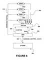
- FIG. 6shows an exemplary embodiment of an interface circuit that is operable to interface memory circuits 602 A-D and a system 604 .
- the interface circuitincludes an AMB 606 and a buffer 608 .
- Address, control, and data signals 620 from the system 604are connected to the AMB 606 .
- the AMB 606drives address and control signals 630 to the memory circuits 602 A-D as well as control signals 640 to the buffer 608 .
- Data signals 650 from the memory circuits 602 A-Dare connected to the buffer 608 .
- Data signals 660are connected between the buffer 608 and the AMB 606 .
- registersregister chip, address/control register chip, data register chip, JEDEC register, etc.
- bufferse.g. buffer chip, multiplexer/de-multiplexer chip, synchronous multiplexer/de-multiplexer chip and/or other intelligent interface circuits
- AMBse.g. AMB chip, etc.
- these register(s), buffer(s), AMB(s)may be utilized alone and/or integrated in groups and/or integrated with or without the memory circuits.
- the electrical connections between the buffer(s), the register(s), the AMB(s) and the memory circuitsmay be configured in any desired manner.
- address, control (e.g. command, etc.), and clock signalsmay be common to all memory circuits (e.g. using one common bus).
- data signalsmay be wired as one common bus, several busses or as an individual bus to each memory circuit.
- the memory circuitsmay have one common address, control and clock bus with individual data busses.
- memory circuitsmay have one, two (or more) address, control and clock busses along with one, two (or more) data busses.
- the memory circuitsmay have one address, control and clock bus together with two data busses (e.g. the number of address, control, clock and data busses may be different, etc.).
- the memory circuitsmay have one common address, control and clock bus and one common data bus. It should be noted that any other permutations and combinations of such address, control, clock and data buses may be utilized.
- the interface circuit(s)may be connected to 1, 2, 4, 8 or more memory circuits. In alternate embodiments, to permit data integrity storage or for other reasons, the interface circuit(s) may be connected to an odd number of memory circuits. Additionally, the memory circuits may be arranged in a single stack. Of course, however, the memory circuits may also be arranged in a plurality of stacks or in any other fashion.
- DRAMe.g. DDR2 SDRAM
- DRAMe.g. DDR2 SDRAM
- portionse.g. ranks, sub-ranks, banks, sub-banks, etc.
- operationse.g. precharge, active, read, write, refresh, etc.
- parallele.g. simultaneously, concurrently, overlapping, etc.
- DRAMe.g. DDR2 SDRAM
- JEDECJEDEC standards and specifications describe how DRAM (e.g. DDR2 SDRAM) circuits are composed and perform operations in response to commands.
- a 512 Mb DDR2 SDRAM circuit that meets JEDEC specificationsmay be composed of four portions (e.g.
- a 2 Gb DDR2 SDRAM circuitthat is compliant with JEDEC specifications may be composed of eight banks (each of which has 256 Mb of capacity).
- a portion (e.g. bank, etc.) of the DRAM circuitis said to be in the active state after an activate command is issued to that portion.
- a portion (e.g. bank, etc.) of the DRAM circuitis said to be in the precharge state after a precharge command is issued to that portion.
- the entire DRAM circuitis said to be in the active state.
- a relative time period spent by the entire DRAM circuit in precharge state with respect to the time period spent by the entire DRAM circuit in active state during normal operationmay be defined as the precharge-to-active ratio.
- DRAM circuitsmay also support a plurality of power management modes. Some of these modes may represent power saving modes. As an example, DDR2 SDRAMs may support four power saving modes. In particular, two active power down modes, precharge power down mode, and self-refresh mode may be supported, in one embodiment.
- a DRAM circuitmay enter an active power down mode if the DRAM circuit is in the active state when it receives a power down command.
- a DRAM circuitmay enter the precharge power down mode if the DRAM circuit is in the precharge state when it receives a power down command.
- a higher precharge-to-active ratiomay increase the likelihood that a DRAM circuit may enter the precharge power down mode rather than an active power down mode when the DRAM circuit is the target of a power saving operation.
- the precharge power down mode and the self refresh modemay provide greater power savings that the active power down modes.
- the systemmay be operable to perform a power management operation on at least one of the memory circuits, and optionally on the interface circuit, based on the state of the at least one memory circuit.
- a power management operationmay include, among others, a power saving operation.
- the term power saving operationmay refer to any operation that results in at least some power savings.
- the power saving operationmay include applying a power saving command to one or more memory circuits, and optionally to the interface circuit, based on at least one state of one or more memory circuits.
- Such power saving commandmay include, for example, initiating a power down operation applied to one or more memory circuits, and optionally to the interface circuit.
- Such statemay depend on identification of the current, past or predictable future status of one or more memory circuits, a predetermined combination of commands to the one or more memory circuits, a predetermined pattern of commands to the one or more memory circuits, a predetermined absence of commands to the one or more memory circuits, any command(s) to the one or more memory circuits, and/or any command(s) to one or more memory circuits other than the one or more memory circuits.
- Such commandsmay have occurred in the past, might be occurring in the present, or may be predicted to occur in the future. Future commands may be predicted since the system (e.g. memory controller, etc.) may be aware of future accesses to the memory circuits in advance of the execution of the commands by the memory circuits.
- such current, past, or predictable future statusmay refer to any property of the memory circuit that may be monitored, stored, and/or predicted.
- the systemmay identify at least one of a plurality of memory circuits that may not be accessed for some period of time. Such status identification may involve determining whether a portion(s) (e.g. bank(s), etc.) is being accessed in at least one of the plurality of memory circuits. Of course, any other technique may be used that results in the identification of at least one of the memory circuits (or portion(s) thereof) that is not being accessed (e.g. in a non-accessed state, etc.). In other embodiments, other such states may be detected or identified and used for power management.
- a portion(s)e.g. bank(s), etc.
- any other techniquemay be used that results in the identification of at least one of the memory circuits (or portion(s) thereof) that is not being accessed (e.g. in a non-accessed state, etc.). In other embodiments, other such states may be detected or identified and used for power management.
- a power saving operationmay be initiated in association with the memory circuit (or portion(s) thereof) that is in the non-accessed state.
- such power saving operationmay involve a power down operation (e.g. entry into an active power down mode, entry into a precharge power down mode, etc.).
- a power management signalincluding, but not limited to a clock enable (CKE) signal, chip select (CS) signal, row address strobe (RAS), column address strobe (CAS), write enable (WE), and optionally in combination with other signals and/or commands.
- CKEclock enable
- CSchip select
- RASrow address strobe
- CAScolumn address strobe
- WEwrite enable
- non-power management signale.g. control signal(s), address signal(s), data signal(s), command(s), etc.
- control signal(s)e.g. address signal(s), data signal(s), command(s), etc.
- the systemmay, in yet another embodiment, be operable to map the physical memory circuits to appear as at least one virtual memory circuit with at least one aspect that is different from that of the physical memory circuits, resulting in a first behavior of the virtual memory circuits that is different from a second behavior of the physical memory circuits.
- the interface circuitmay be operable to aid or participate in the mapping of the physical memory circuits such that they appear as at least one virtual memory circuit.
- the physical memory circuitsmay be mapped to appear as at least one virtual memory circuit with at least one aspect that is different from that of the physical memory circuits, resulting in a first behavior of the at least one virtual memory circuits that is different from a second behavior of one or more of the physical memory circuits.
- Such behaviormay, in one embodiment, include power behavior (e.g. a power consumption, current consumption, current waveform, any other aspect of power management or behavior, etc.).
- power behavior simulationmay effect or result in a reduction or other modification of average power consumption, reduction or other modification of peak power consumption or other measure of power consumption, reduction or other modification of peak current consumption or other measure of current consumption, and/or modification of other power behavior (e.g. parameters, metrics, etc.).
- the at least one aspect that is altered by the simulationmay be the precharge-to-active ratio of the physical memory circuits.
- the alteration of such a ratiomay be fixed (e.g. constant, etc.) or may be variable (e.g. dynamic, etc.).
- a fixed alteration of this ratiomay be accomplished by a simulation that results in physical memory circuits appearing to have fewer portions (e.g. banks, etc.) that may be capable of performing operations in parallel.
- a physical 1 Gb DDR2 SDRAM circuit with eight physical banksmay be mapped to a virtual 1 Gb DDR2 SDRAM circuit with two virtual banks, by coalescing or combining four physical banks into one virtual bank.
- Such a simulationmay increase the precharge-to-active ratio of the virtual memory circuit since the virtual memory circuit now has fewer portions (e.g. banks, etc.) that may be in use (e.g. in an active state, etc.) at any given time.
- a physical 1 Gb DDR2 SDRAM circuit with eight physical banksmay have a probability, g, that all eight physical banks are in the precharge state at any given time.
- the virtual DDR2 SDRAM circuitmay have a probability, h, that both the virtual banks are in the precharge state at any given time. Under normal operating conditions of the system, h may be greater than g.
- a power saving operation directed at the aforementioned virtual 1 Gb DDR2 SDRAM circuitmay have a higher likelihood of placing the DDR2 SDRAM circuit in a precharge power down mode as compared to a similar power saving operation directed at the aforementioned physical 1 Gb DDR2 SDRAM circuit.
- a virtual memory circuit with fewer portions (e.g. banks, etc.) than a physical memory circuit with equivalent capacitymay not be compatible with certain industry standards (e.g. JEDEC standards).
- JEDEC standardse.g. JEDEC standards
- the JEDEC Standard No. JESD 21-C for DDR2 SDRAMspecifics a 1 Gb DRAM circuit with eight banks.
- a 1 Gb virtual DRAM circuit with two virtual banksmay not be compliant with the JEDEC standard.
- a plurality of physical memory circuits, each having a first number of physical portionse.g.
- each physical memory circuit that is part of the at least one virtual memory circuithas a second number of portions (e.g. banks, etc.) that may be capable of performing operations in parallel, wherein the second number of portions is different from the first number of portions.
- four physical 1 Gb DDR2 SDRAM circuits(each with eight physical banks) may be mapped to a single virtual 4 Gb DDR2 SDRAM circuit with eight virtual banks, wherein the eight physical banks in each physical 1 Gb DDR2 SDRAM circuit have been coalesced or combined into two virtual banks.
- four physical 1 Gb DDR2 SDRAM circuitsmay be mapped to two virtual 2 Gb DDR2 SDRAM circuits, each with eight virtual banks, wherein the eight physical banks in each physical 1 Gb DDR2 SDRAM circuit have been coalesced or combined into four virtual banks.
- the interface circuitmay be operable to aid the system in the mapping of the physical memory circuits.
- FIG. 7shows an example of four physical 1 Gb DDR2 SDRAM circuits 702 A-D that are mapped by the system 706 , and optionally with the aid or participation of interface circuit 704 , to appear as a virtual 4 Gb DDR2 SDRAM circuit 708 .
- Each physical DRAM circuit 702 A-D containing eight physical banks 720has been mapped to two virtual banks 730 of the virtual 4 Gb DDR2 SDRAM circuit 708 .
- the simulation or mappingresults in the memory circuits having fewer portions (e.g. banks etc.) that may be capable of performing operations in parallel.
- this simulationmay be done by mapping (e.g. coalescing or combining) a first number of physical portion(s) (e.g. banks, etc.) into a second number of virtual portion(s). If the second number is less than the first number, a memory circuit may have fewer portions that may be in use at any given time. Thus, there may be a higher likelihood that a power saving operation targeted at such a memory circuit may result in that particular memory circuit consuming less power.
- a variable change in the precharge-to-active ratiomay be accomplished by a simulation that results in the at least one virtual memory circuit having at least one latency that is different from that of the physical memory circuits.
- a physical 1 Gb DDR2 SDRAM circuit with eight banksmay be mapped by the system, and optionally the interface circuit, to appear as a virtual 1 Gb DDR2 SDRAM circuit with eight virtual banks having at least one latency that is different from that of the physical DRAM circuits.
- the latencymay include one or more timing parameters such as tFAW, tRRD, tRP, tRCD, tRFC(MIN), etc.
- tFAWis the 4-Bank activate period
- tRRDis the ACTIVE bank a to ACTIVE bank b command timing parameter
- tRPis the PRECHARGE command period
- tRCDis the ACTIVE-to-READ or WRITE delay
- tRFC(min)is the minimum value of the REFRESH to ACTIVE or REFRESH to REFRESH command interval.
- these and other DRAM timing parametersare defined in the JEDEC specifications (for example JESD 21-C for DDR2 SDRAM and updates, corrections and errata available at the JEDEC website) as well as the DRAM manufacturer datasheets (for example the MICRON datasheet for 1 Gb: .times.4, .times.8, .times.16 DDR2 SDRAM, example part number MT47H256M4, labeled PDF: 09005aef821ae8bf/Source: 09005aef821aed36, 1 GbDDR2TOC.fm-Rev. K 9/06 EN, and available at the MICRON website).
- JEDEC specificationsfor example JESD 21-C for DDR2 SDRAM and updates, corrections and errata available at the JEDEC website
- DRAM manufacturer datasheetsfor example the MICRON datasheet for 1 Gb: .times.4, .times.8, .times.16 DDR2 SDRAM, example part number
- the virtual DRAM circuitmay be simulated to have a tRP(virtual) that is greater than the tRP(physical) of the physical DRAM circuit. Such a simulation may thus increase the minimum latency between a precharge command and a subsequent activate command to a portion (e.g. bank, etc.) of the virtual DRAM circuit.
- the virtual DRAM circuitmay be simulated to have a tRRD(virtual) that is greater than the tRRD(physical) of the physical DRAM circuit.
- Such a simulationmay thus increase the minimum latency between successive activate commands to various portions (e.g. banks, etc.) of the virtual DRAM circuit.
- Such simulationsmay increase the precharge-to-active ratio of the memory circuit.
- the systemmay optionally change the values of one or more latencies of the at least one virtual memory circuit in response to present, past, or future commands to the memory circuits, the temperature of the memory circuits, etc. That is, the at least one aspect of the virtual memory circuit may be changed dynamically.
- Some memory busesmay allow the use of 1T or 2T address timing (also known as 1T or 2T address clocking).
- 1T or 2T address timingalso known as 1T or 2T address clocking.
- the MICRON technical note TN-47-01, DDR2 DESIGN GUIDE FOR TWO-DIMM SYSTEMS(available at the MICRON website) explains the meaning and use of 1T and 2T address timing as follows: “Further, the address bus can be clocked using 1T or 2T clocking. With 1T, a new command can be issued on every clock cycle 2T timing will hold the address and command bus valid for two clock cycles. This reduces the efficiency of the bus to one command per two clocks, but it doubles the amount of setup and hold time. The data bus remains the same for all of the variations in the address bus.”
- the systemmay change the precharge-to-active ratio of the virtual memory circuit by changing from 1T address timing to 2T address timing when sending addresses and control signals to the interface circuit and/or the memory circuits. Since 2T address timing affects the latency between successive commands to the memory circuits, the precharge-to-active ratio of a memory circuit may be changed. Strictly as an option, the system may dynamically change between 1T and 2T address timing.
- the systemmay communicate a first number of power management signals to the interface circuit to control the power behavior.
- the interface circuitmay communicate a second number of power management signals to at least a portion of the memory circuits.
- the second number of power management signalsmay be the same of different from the first number of power management signals.
- the second number of power management signalsmay be utilized to perform power management of the portion(s) of the virtual or physical memory circuits in a manner that is independent from each other and/or independent from the first number of power management signals received from the system (which may or may not also be utilized in a manner that is independent from each other).
- the systemmay provide power management signals directly to the memory circuits.
- such power management signal(s)may refer to any control signal (e.g. one or more address signals; one or more data signals; a combination of one or more control signals; a sequence of one or more control signals; a signal associated with an active (or active) operation, precharge operation, write operation, read operation, a mode register write operation, a mode register read operation, a refresh operation, or other encoded or direct operation, command or control signal, etc.).
- the operation associated with a commandmay consist of the command itself and optionally, one or more necessary signals and/or behavior.
- the power management signals received from the systemmay be individual signals supplied to a DIMM.
- the power management signalsmay include, for example, CKE and CS signals. These power management signals may also be used in conjunction and/or combination with each other, and optionally, with other signals and commands that are encoded using other signals (e.g. RAS, CAS, WE, address etc.) for example.
- the JEDEC standardsmay be describe how commands directed to memory circuits are to be encoded. As the number of memory circuits on a DIMM is increased, it is beneficial to increase the number of power management signals so as to increase the flexibility of the system to manage portion(s) of the memory circuits on a DIMM.
- the power management signalsmay take several forms.
- the power management signalsmay be encoded, located, placed, or multiplexed in various existing fields (e.g. data field, address field, etc.), signals (e.g. CKE signal, CD signal, etc.), and/or busses.
- a signalmay be a single wire; that is a single electrical point-to-point connection.
- the signalis un-encoded and not bussed, multiplexed, or encoded.
- a command directed to a memory circuitmay be encoded, for example, in an address signal, by setting a predefined number of bits in a predefined location (or field) on the address bus to a specific combination that uniquely identifies that command.
- the commandis said to be encoded on the address bus and located or placed in a certain position, location, or field.
- multiple bits of informationmay be placed on multiple wires that form a bus.
- a signal that requires the transfer of two or more bits of informationmay be time-multiplexed onto a single wire.
- the time-multiplexed sequence of 10(a one followed by a zero) may be made equivalent to two individual signals: a one and a zero.
- Such examples of time-multiplexingare another form of encoding.
- Such various well-known methods of signaling, encoding (or lack thereof), bussing, and multiplexing, etc.may be used in isolation or combination.
- the power management signals from the systemmay occupy currently unused connection pins on a DIMM (unused pins may be specified by the JEDEC standards).
- the power management signalsmay use existing CKE and CS pins on a DIMM, according to the JEDEC standard, along with additional CKE and CD pins to enable, for example, power management of DIMM capacities that may not yet be currently defined by the JEDEC standards.
- the power management signals from the systemmay be encoded in the CKE and CS signals.
- the CKE signalmay be a bus, and the power management signals may be encoded on that bus.
- a 3-bit wide buscomprising three signals on three separate wires: CKE[ 0 ], CKE[ 1 ], and CKE[ 2 ], may be decoded by the interface circuit to produce eight separate CKE signals that comprise the power management signals for the memory circuits.
- the power management signals from the systemmay be encoded in unused portions of existing fields.
- certain commandsmay have portions of the fields set to X (also known as don't care).
- Xalso known as don't care
- the setting of such bit(s) to either a one or to a zerodoes not affect the command.
- the effectively unused bit position in this fieldmay thus be used to carry a power management signal.
- the power management signalmay thus be encoded and located or placed in a field in a bus, for example.
- the power management schemes described for the DRAM circuitsmay also be extended to the interface circuits.
- the systemmay have or may infer information that a signal, bus, or other connection will not be used for a period of time. During this period of time, the system may perform power management on the interface circuit or part(s) thereof.
- Such power managementmay, for example, use an intelligent signaling mechanism (e.g. encoded signals, sideband signals, etc.) between the system and interface circuits (e.g. register chips, buffer chips, AMB chips, etc.), and/or between interface circuits. These signals may be used to power manage (e.g.
- the interface circuitse.g. input receiver circuits, internal logic circuits, clock generation circuits, output driver circuits, termination circuits, etc.
- FIG. 8illustrates an embodiment of a multiple memory circuit framework that is similar to the multiple memory framework in FIG. 1 .
- FIG. 8shows a memory controller 850 within the system 106 .
- the interface circuit 102is configured to communicate with the memory controller 850 via bus 852 .
- FIG. 9shows an exemplary embodiment of an interface circuit that is operable to interface memory circuits 202 A-D and a system 204 similar to the exemplary embodiment in FIG. 2 .
- the plurality of memory circuits 202 A-Dis a plurality of dynamic random access memory (DRAM) circuits in a dual in-line memory module (DIMM) 952 .
- DRAMdynamic random access memory
- FIG. 10is a flowchart showing an embodiment of a method for simulating at least one virtual memory circuit.
- the methodincludes interfacing (at 1060 ) a plurality of physical memory circuits and a memory controller using an interface circuit, wherein the interface circuit is configured to communicate with the memory controller via a bus.
- the methodalso includes simulating (at 1062 ) at least one virtual memory circuit for the memory controller, wherein a precharge-to-active ratio of the simulated virtual memory circuit is different from a precharge-to-active ratio of at least one physical memory circuit of the plurality of physical memory circuits.
- the methodalso includes changing (at 1064 ) in a timing of the bus to change the precharge-to-active ratio of the simulated virtual memory circuit.
- the change in the timing of the busis a change from a first address timing to a second address timing.
- the first address timingcan be a 1 T address timing and the second address timing is a 2T address timing.
- commands or signals on the busare valid for one clock cycle when the 1T address timing is used, whereas commands or signals on the bus are valid for two clock cycles when the 2T address timing is used.
- the methodalso includes placing (at 1066 ), with the memory controller, power management signals in at least one of an address field, a data field, at least one unused pin on a dual in-line memory module (DIMM), a clock enable signal, and a chip select signal.
- DIMMdual in-line memory module
- the methodalso includes changing (at 1068 ), with the interface circuit, power-related aspects of the simulated virtual memory circuit based on power management signals received from the memory controller.
- a plurality of memory circuitsmay be mapped using simulation to appear as at least one virtual memory circuit, wherein a first number of portions (e.g. banks, etc.) in each physical memory circuit may be coalesced or combined into a second number of virtual portions (e.g. banks, etc.), and the at least one virtual memory circuit may have at least one latency that is different from the corresponding latency of the physical memory circuits.
- the first and second number of portionsmay include any one or more portions.
Landscapes
- Engineering & Computer Science (AREA)
- Computer Hardware Design (AREA)
- Microelectronics & Electronic Packaging (AREA)
- Power Engineering (AREA)
- Physics & Mathematics (AREA)
- Theoretical Computer Science (AREA)
- Evolutionary Computation (AREA)
- Geometry (AREA)
- General Engineering & Computer Science (AREA)
- General Physics & Mathematics (AREA)
- Dram (AREA)
Abstract
Description
Claims (22)
Priority Applications (3)
| Application Number | Priority Date | Filing Date | Title |
|---|---|---|---|
| US12/816,756US8122207B2 (en) | 2006-07-31 | 2010-06-16 | Apparatus and method for power management of memory circuits by a system or component thereof |
| US13/343,612US8407412B2 (en) | 2006-07-31 | 2012-01-04 | Power management of memory circuits by virtual memory simulation |
| US13/620,601US8972673B2 (en) | 2006-07-31 | 2012-09-14 | Power management of memory circuits by virtual memory simulation |
Applications Claiming Priority (4)
| Application Number | Priority Date | Filing Date | Title |
|---|---|---|---|
| US11/461,439US7580312B2 (en) | 2006-07-31 | 2006-07-31 | Power saving system and method for use with a plurality of memory circuits |
| US11/524,811US7590796B2 (en) | 2006-07-31 | 2006-09-20 | System and method for power management in memory systems |
| US11/538,041US20080082763A1 (en) | 2006-10-02 | 2006-10-02 | Apparatus and method for power management of memory circuits by a system or component thereof |
| US12/816,756US8122207B2 (en) | 2006-07-31 | 2010-06-16 | Apparatus and method for power management of memory circuits by a system or component thereof |
Related Parent Applications (1)
| Application Number | Title | Priority Date | Filing Date |
|---|---|---|---|
| US11/538,041ContinuationUS20080082763A1 (en) | 2005-06-24 | 2006-10-02 | Apparatus and method for power management of memory circuits by a system or component thereof |
Related Child Applications (1)
| Application Number | Title | Priority Date | Filing Date |
|---|---|---|---|
| US13/343,612ContinuationUS8407412B2 (en) | 2006-07-31 | 2012-01-04 | Power management of memory circuits by virtual memory simulation |
Publications (2)
| Publication Number | Publication Date |
|---|---|
| US20100257304A1 US20100257304A1 (en) | 2010-10-07 |
| US8122207B2true US8122207B2 (en) | 2012-02-21 |
Family
ID=39262367
Family Applications (4)
| Application Number | Title | Priority Date | Filing Date |
|---|---|---|---|
| US11/538,041AbandonedUS20080082763A1 (en) | 2005-06-24 | 2006-10-02 | Apparatus and method for power management of memory circuits by a system or component thereof |
| US12/816,756ActiveUS8122207B2 (en) | 2006-07-31 | 2010-06-16 | Apparatus and method for power management of memory circuits by a system or component thereof |
| US13/343,612Expired - Fee RelatedUS8407412B2 (en) | 2006-07-31 | 2012-01-04 | Power management of memory circuits by virtual memory simulation |
| US13/620,601ActiveUS8972673B2 (en) | 2006-07-31 | 2012-09-14 | Power management of memory circuits by virtual memory simulation |
Family Applications Before (1)
| Application Number | Title | Priority Date | Filing Date |
|---|---|---|---|
| US11/538,041AbandonedUS20080082763A1 (en) | 2005-06-24 | 2006-10-02 | Apparatus and method for power management of memory circuits by a system or component thereof |
Family Applications After (2)
| Application Number | Title | Priority Date | Filing Date |
|---|---|---|---|
| US13/343,612Expired - Fee RelatedUS8407412B2 (en) | 2006-07-31 | 2012-01-04 | Power management of memory circuits by virtual memory simulation |
| US13/620,601ActiveUS8972673B2 (en) | 2006-07-31 | 2012-09-14 | Power management of memory circuits by virtual memory simulation |
Country Status (1)
| Country | Link |
|---|---|
| US (4) | US20080082763A1 (en) |
Cited By (11)
| Publication number | Priority date | Publication date | Assignee | Title |
|---|---|---|---|---|
| US8407412B2 (en)* | 2006-07-31 | 2013-03-26 | Google Inc. | Power management of memory circuits by virtual memory simulation |
| US8930647B1 (en) | 2011-04-06 | 2015-01-06 | P4tents1, LLC | Multiple class memory systems |
| US9123441B1 (en) | 2014-04-04 | 2015-09-01 | Inphi Corporation | Backward compatible dynamic random access memory device and method of testing therefor |
| US9158546B1 (en) | 2011-04-06 | 2015-10-13 | P4tents1, LLC | Computer program product for fetching from a first physical memory between an execution of a plurality of threads associated with a second physical memory |
| US9164679B2 (en) | 2011-04-06 | 2015-10-20 | Patents1, Llc | System, method and computer program product for multi-thread operation involving first memory of a first memory class and second memory of a second memory class |
| US9170744B1 (en) | 2011-04-06 | 2015-10-27 | P4tents1, LLC | Computer program product for controlling a flash/DRAM/embedded DRAM-equipped system |
| US9176671B1 (en) | 2011-04-06 | 2015-11-03 | P4tents1, LLC | Fetching data between thread execution in a flash/DRAM/embedded DRAM-equipped system |
| US9417754B2 (en) | 2011-08-05 | 2016-08-16 | P4tents1, LLC | User interface system, method, and computer program product |
| US10198187B1 (en) | 2015-10-16 | 2019-02-05 | Rambus Inc. | Buffering device with status communication method for memory controller |
| US10628624B1 (en)* | 2018-08-14 | 2020-04-21 | Cadence Design Systems, Inc. | System and method for simulating channels using true strobe timing |
| US11742046B2 (en) | 2020-09-03 | 2023-08-29 | Samsung Electronics Co., Ltd. | Semiconductor memory device and operation method of swizzling data |
Families Citing this family (70)
| Publication number | Priority date | Publication date | Assignee | Title |
|---|---|---|---|---|
| KR20050022798A (en)* | 2003-08-30 | 2005-03-08 | 주식회사 이즈텍 | A system for analyzing bio chips using gene ontology, and a method thereof |
| US8796830B1 (en) | 2006-09-01 | 2014-08-05 | Google Inc. | Stackable low-profile lead frame package |
| US10013371B2 (en) | 2005-06-24 | 2018-07-03 | Google Llc | Configurable memory circuit system and method |
| US9542352B2 (en) | 2006-02-09 | 2017-01-10 | Google Inc. | System and method for reducing command scheduling constraints of memory circuits |
| US20080028136A1 (en)* | 2006-07-31 | 2008-01-31 | Schakel Keith R | Method and apparatus for refresh management of memory modules |
| KR101377305B1 (en) | 2005-06-24 | 2014-03-25 | 구글 인코포레이티드 | An integrated memory core and memory interface circuit |
| US8060774B2 (en)* | 2005-06-24 | 2011-11-15 | Google Inc. | Memory systems and memory modules |
| US8244971B2 (en) | 2006-07-31 | 2012-08-14 | Google Inc. | Memory circuit system and method |
| US8041881B2 (en) | 2006-07-31 | 2011-10-18 | Google Inc. | Memory device with emulated characteristics |
| US7386656B2 (en) | 2006-07-31 | 2008-06-10 | Metaram, Inc. | Interface circuit system and method for performing power management operations in conjunction with only a portion of a memory circuit |
| US8081474B1 (en) | 2007-12-18 | 2011-12-20 | Google Inc. | Embossed heat spreader |
| US8397013B1 (en) | 2006-10-05 | 2013-03-12 | Google Inc. | Hybrid memory module |
| US8089795B2 (en) | 2006-02-09 | 2012-01-03 | Google Inc. | Memory module with memory stack and interface with enhanced capabilities |
| US8438328B2 (en) | 2008-02-21 | 2013-05-07 | Google Inc. | Emulation of abstracted DIMMs using abstracted DRAMs |
| US8335894B1 (en) | 2008-07-25 | 2012-12-18 | Google Inc. | Configurable memory system with interface circuit |
| US8111566B1 (en) | 2007-11-16 | 2012-02-07 | Google, Inc. | Optimal channel design for memory devices for providing a high-speed memory interface |
| US7609567B2 (en)* | 2005-06-24 | 2009-10-27 | Metaram, Inc. | System and method for simulating an aspect of a memory circuit |
| US8055833B2 (en) | 2006-10-05 | 2011-11-08 | Google Inc. | System and method for increasing capacity, performance, and flexibility of flash storage |
| US7392338B2 (en) | 2006-07-31 | 2008-06-24 | Metaram, Inc. | Interface circuit system and method for autonomously performing power management operations in conjunction with a plurality of memory circuits |
| US8077535B2 (en) | 2006-07-31 | 2011-12-13 | Google Inc. | Memory refresh apparatus and method |
| US8130560B1 (en) | 2006-11-13 | 2012-03-06 | Google Inc. | Multi-rank partial width memory modules |
| US8090897B2 (en) | 2006-07-31 | 2012-01-03 | Google Inc. | System and method for simulating an aspect of a memory circuit |
| US8386722B1 (en) | 2008-06-23 | 2013-02-26 | Google Inc. | Stacked DIMM memory interface |
| US9507739B2 (en) | 2005-06-24 | 2016-11-29 | Google Inc. | Configurable memory circuit system and method |
| US9171585B2 (en) | 2005-06-24 | 2015-10-27 | Google Inc. | Configurable memory circuit system and method |
| US8327104B2 (en) | 2006-07-31 | 2012-12-04 | Google Inc. | Adjusting the timing of signals associated with a memory system |
| US8359187B2 (en) | 2005-06-24 | 2013-01-22 | Google Inc. | Simulating a different number of memory circuit devices |
| WO2007028109A2 (en) | 2005-09-02 | 2007-03-08 | Metaram, Inc. | Methods and apparatus of stacking drams |
| US7562271B2 (en) | 2005-09-26 | 2009-07-14 | Rambus Inc. | Memory system topologies including a buffer device and an integrated circuit memory device |
| US11328764B2 (en) | 2005-09-26 | 2022-05-10 | Rambus Inc. | Memory system topologies including a memory die stack |
| US9632929B2 (en) | 2006-02-09 | 2017-04-25 | Google Inc. | Translating an address associated with a command communicated between a system and memory circuits |
| US7724589B2 (en)* | 2006-07-31 | 2010-05-25 | Google Inc. | System and method for delaying a signal communicated from a system to at least one of a plurality of memory circuits |
| US20080091888A1 (en)* | 2006-10-17 | 2008-04-17 | Motorola, Inc. | Memory system having baseboard located memory buffer unit |
| US8019938B2 (en) | 2006-12-06 | 2011-09-13 | Fusion-I0, Inc. | Apparatus, system, and method for solid-state storage as cache for high-capacity, non-volatile storage |
| US8874831B2 (en) | 2007-06-01 | 2014-10-28 | Netlist, Inc. | Flash-DRAM hybrid memory module |
| US8209479B2 (en) | 2007-07-18 | 2012-06-26 | Google Inc. | Memory circuit system and method |
| US8080874B1 (en) | 2007-09-14 | 2011-12-20 | Google Inc. | Providing additional space between an integrated circuit and a circuit board for positioning a component therebetween |
| US7836226B2 (en) | 2007-12-06 | 2010-11-16 | Fusion-Io, Inc. | Apparatus, system, and method for coordinating storage requests in a multi-processor/multi-thread environment |
| US8719606B2 (en)* | 2008-03-31 | 2014-05-06 | Intel Corporation | Optimizing performance and power consumption during memory power down state |
| WO2010016818A1 (en)* | 2008-08-08 | 2010-02-11 | Hewlett-Packard Development Company, L.P. | Independently controlled virtual memory devices in memory modules |
| US8880772B2 (en)* | 2009-05-29 | 2014-11-04 | Dell Products L.P. | System and method for serial interface topologies |
| DE202010017690U1 (en) | 2009-06-09 | 2012-05-29 | Google, Inc. | Programming dimming terminating resistor values |
| US9021158B2 (en) | 2009-09-09 | 2015-04-28 | SanDisk Technologies, Inc. | Program suspend/resume for memory |
| WO2011031899A2 (en) | 2009-09-09 | 2011-03-17 | Fusion-Io, Inc. | Apparatus, system, and method for power reduction in a storage device |
| US9223514B2 (en) | 2009-09-09 | 2015-12-29 | SanDisk Technologies, Inc. | Erase suspend/resume for memory |
| US8984216B2 (en) | 2010-09-09 | 2015-03-17 | Fusion-Io, Llc | Apparatus, system, and method for managing lifetime of a storage device |
| KR101796116B1 (en) | 2010-10-20 | 2017-11-10 | 삼성전자 주식회사 | Semiconductor device, memory module and memory system having the same and operating method thereof |
| US9047178B2 (en) | 2010-12-13 | 2015-06-02 | SanDisk Technologies, Inc. | Auto-commit memory synchronization |
| US10817421B2 (en) | 2010-12-13 | 2020-10-27 | Sandisk Technologies Llc | Persistent data structures |
| CN103262054B (en) | 2010-12-13 | 2015-11-25 | 桑迪士克科技股份有限公司 | For automatically submitting device, the system and method for storer to |
| US9218278B2 (en) | 2010-12-13 | 2015-12-22 | SanDisk Technologies, Inc. | Auto-commit memory |
| US9208071B2 (en) | 2010-12-13 | 2015-12-08 | SanDisk Technologies, Inc. | Apparatus, system, and method for accessing memory |
| US10817502B2 (en) | 2010-12-13 | 2020-10-27 | Sandisk Technologies Llc | Persistent memory management |
| WO2012109677A2 (en) | 2011-02-11 | 2012-08-16 | Fusion-Io, Inc. | Apparatus, system, and method for managing operations for data storage media |
| US9432298B1 (en) | 2011-12-09 | 2016-08-30 | P4tents1, LLC | System, method, and computer program product for improving memory systems |
| WO2013100909A1 (en)* | 2011-12-27 | 2013-07-04 | Intel Corporation | Adaptive configuration of non-volatile memory |
| US9251086B2 (en) | 2012-01-24 | 2016-02-02 | SanDisk Technologies, Inc. | Apparatus, system, and method for managing a cache |
| TWI459400B (en)* | 2012-04-17 | 2014-11-01 | Phison Electronics Corp | Memory stroage apparatus, and memolry controller and power control method |
| TWI512623B (en)* | 2013-12-26 | 2015-12-11 | Phison Electronics Corp | Method of enabling sleep mode, memory control circuit unit and storage apparatus |
| US9666244B2 (en) | 2014-03-01 | 2017-05-30 | Fusion-Io, Inc. | Dividing a storage procedure |
| US9933950B2 (en) | 2015-01-16 | 2018-04-03 | Sandisk Technologies Llc | Storage operation interrupt |
| US11222551B2 (en)* | 2015-07-23 | 2022-01-11 | Rockwell Automation Technologies, Inc. | Snapshot management architecture for process control operator training system lifecycle |
| KR20170075359A (en)* | 2015-12-23 | 2017-07-03 | 에스케이하이닉스 주식회사 | Memory system and operation method of memory controller |
| US10679722B2 (en) | 2016-08-26 | 2020-06-09 | Sandisk Technologies Llc | Storage system with several integrated components and method for use therewith |
| KR102807152B1 (en)* | 2016-11-01 | 2025-05-13 | 에스케이하이닉스 주식회사 | Memory device and memory system supporting rank-level parallelism |
| US10769082B2 (en)* | 2018-05-01 | 2020-09-08 | Integrated Device Technology, Inc. | DDR5 PMIC interface protocol and operation |
| US10776293B2 (en)* | 2018-05-01 | 2020-09-15 | Integrated Device Technology, Inc. | DDR5 RCD interface protocol and operation |
| US11538507B1 (en)* | 2021-08-30 | 2022-12-27 | Taiwan Semiconductor Manufacturing Company, Ltd. | Header circuit placement in memory device |
| US20220012173A1 (en)* | 2021-09-24 | 2022-01-13 | Intel Corporation | Flexible configuration of memory module data width |
| US12411537B2 (en) | 2022-01-26 | 2025-09-09 | Samsung Electronics Co., Ltd. | Power reduction for systems having multiple ranks of memory |
Citations (196)
| Publication number | Priority date | Publication date | Assignee | Title |
|---|---|---|---|---|
| US3800292A (en) | 1972-10-05 | 1974-03-26 | Honeywell Inf Systems | Variable masking for segmented memory |
| US4069452A (en) | 1976-09-15 | 1978-01-17 | Dana Laboratories, Inc. | Apparatus for automatically detecting values of periodically time varying signals |
| US4334307A (en) | 1979-12-28 | 1982-06-08 | Honeywell Information Systems Inc. | Data processing system with self testing and configuration mapping capability |
| US4345319A (en) | 1978-06-28 | 1982-08-17 | Cselt-Centro Studi E Laboratori Telecomunicazioni S.P.A. | Self-correcting, solid-state-mass-memory organized by bits and with reconfiguration capability for a stored program control system |
| US4566082A (en) | 1983-03-23 | 1986-01-21 | Tektronix, Inc. | Memory pack addressing system |
| US4794597A (en) | 1986-03-28 | 1988-12-27 | Mitsubishi Denki Kabushiki Kaisha | Memory device equipped with a RAS circuit |
| US4862347A (en) | 1986-04-22 | 1989-08-29 | International Business Machine Corporation | System for simulating memory arrays in a logic simulation machine |
| US4912678A (en) | 1987-09-26 | 1990-03-27 | Mitsubishi Denki Kabushiki Kaisha | Dynamic random access memory device with staggered refresh |
| US4922451A (en) | 1987-03-23 | 1990-05-01 | International Business Machines Corporation | Memory re-mapping in a microcomputer system |
| US4937791A (en) | 1988-06-02 | 1990-06-26 | The California Institute Of Technology | High performance dynamic ram interface |
| US4956694A (en) | 1988-11-04 | 1990-09-11 | Dense-Pac Microsystems, Inc. | Integrated circuit chip stacking |
| US5025364A (en) | 1987-06-29 | 1991-06-18 | Hewlett-Packard Company | Microprocessor emulation system with memory mapping using variable definition and addressing of memory space |
| US5193072A (en) | 1990-12-21 | 1993-03-09 | Vlsi Technology, Inc. | Hidden refresh of a dynamic random access memory |
| US5390334A (en) | 1990-10-29 | 1995-02-14 | International Business Machines Corporation | Workstation power management by page placement control |
| EP0644547A2 (en) | 1993-09-13 | 1995-03-22 | International Business Machines Corporation | Integrated multichip memory module, structure and fabrication |
| US5502333A (en) | 1994-03-30 | 1996-03-26 | International Business Machines Corporation | Semiconductor stack structures and fabrication/sparing methods utilizing programmable spare circuit |
| US5513135A (en) | 1994-12-02 | 1996-04-30 | International Business Machines Corporation | Synchronous memory packaged in single/dual in-line memory module and method of fabrication |
| US5513339A (en) | 1992-09-30 | 1996-04-30 | At&T Corp. | Concurrent fault simulation of circuits with both logic elements and functional circuits |
| US5519832A (en) | 1992-11-13 | 1996-05-21 | Digital Equipment Corporation | Method and apparatus for displaying module diagnostic results |
| US5550781A (en) | 1989-05-08 | 1996-08-27 | Hitachi Maxell, Ltd. | Semiconductor apparatus with two activating modes of different number of selected word lines at refreshing |
| US5608262A (en) | 1995-02-24 | 1997-03-04 | Lucent Technologies Inc. | Packaging multi-chip modules without wire-bond interconnection |
| US5692121A (en) | 1995-04-14 | 1997-11-25 | International Business Machines Corporation | Recovery unit for mirrored processors |
| USRE35733E (en) | 1991-11-26 | 1998-02-17 | Circuit Components Incorporated | Device for interconnecting integrated circuit packages to circuit boards |
| US5742792A (en) | 1993-04-23 | 1998-04-21 | Emc Corporation | Remote data mirroring |
| US5760478A (en) | 1996-08-20 | 1998-06-02 | International Business Machines Corporation | Clock skew minimization system and method for integrated circuits |
| US5787457A (en) | 1996-10-18 | 1998-07-28 | International Business Machines Corporation | Cached synchronous DRAM architecture allowing concurrent DRAM operations |
| US5819065A (en) | 1995-06-28 | 1998-10-06 | Quickturn Design Systems, Inc. | System and method for emulating memory |
| US5831833A (en) | 1995-07-17 | 1998-11-03 | Nec Corporation | Bear chip mounting printed circuit board and a method of manufacturing thereof by photoetching |
| US5838165A (en) | 1996-08-21 | 1998-11-17 | Chatter; Mukesh | High performance self modifying on-the-fly alterable logic FPGA, architecture and method |
| US5870350A (en) | 1997-05-21 | 1999-02-09 | International Business Machines Corporation | High performance, high bandwidth memory bus architecture utilizing SDRAMs |
| US5872907A (en) | 1991-12-16 | 1999-02-16 | International Business Machines Corporation | Fault tolerant design for identification of AC defects including variance of cycle time to maintain system operation |
| US5878279A (en) | 1995-08-03 | 1999-03-02 | Sgs-Thomson Microelectronics S.A. | HDLC integrated circuit using internal arbitration to prioritize access to a shared internal bus amongst a plurality of devices |
| US5913072A (en) | 1997-04-08 | 1999-06-15 | Wieringa; Fred | Image processing system in which image processing programs stored in a personal computer are selectively executed through user interface of a scanner |
| US5915167A (en) | 1997-04-04 | 1999-06-22 | Elm Technology Corporation | Three dimensional structure memory |
| US5963429A (en) | 1997-08-20 | 1999-10-05 | Sulzer Intermedics Inc. | Printed circuit substrate with cavities for encapsulating integrated circuits |
| US5995424A (en) | 1997-07-16 | 1999-11-30 | Tanisys Technology, Inc. | Synchronous memory test system |
| US6001671A (en) | 1996-04-18 | 1999-12-14 | Tessera, Inc. | Methods for manufacturing a semiconductor package having a sacrificial layer |
| US6047073A (en) | 1994-11-02 | 2000-04-04 | Advanced Micro Devices, Inc. | Digital wavetable audio synthesizer with delay-based effects processing |
| US6058451A (en) | 1997-12-22 | 2000-05-02 | Emc Corporation | Method and apparatus for refreshing a non-clocked memory |
| US6101564A (en) | 1995-08-03 | 2000-08-08 | Sgs-Thomson Microelectronics S.A. | Device for organizing the access to a memory bus |
| US6226709B1 (en) | 1997-10-24 | 2001-05-01 | Compaq Computer Corporation | Memory refresh control system |
| US20010003198A1 (en) | 1999-11-30 | 2001-06-07 | Chung-Che Wu | Method for timing setting of a system memory |
| US20010011322A1 (en) | 1998-06-22 | 2001-08-02 | Patrick F. Stolt | Data strobe for faster data access from a memory array |
| US20010019509A1 (en) | 1999-12-22 | 2001-09-06 | Ari Aho | Memory controller |
| US20010046129A1 (en) | 2000-05-24 | 2001-11-29 | International Business Machines Corporation | Interposer for connecting two substrates and resulting assembly |
| US20010046163A1 (en) | 2000-05-19 | 2001-11-29 | Fujitsu Limited | Memory system and memory controller with reliable data latch operation |
| US6336174B1 (en) | 1999-08-09 | 2002-01-01 | Maxtor Corporation | Hardware assisted memory backup system and method |
| US20020002662A1 (en)* | 1998-07-13 | 2002-01-03 | Olarig Sompong Paul | Method and apparatus for supporting heterogeneous memory in computer systems |
| US20020004897A1 (en) | 2000-07-05 | 2002-01-10 | Min-Cheng Kao | Data processing apparatus for executing multiple instruction sets |
| US20020015340A1 (en) | 2000-07-03 | 2002-02-07 | Victor Batinovich | Method and apparatus for memory module circuit interconnection |
| US20020060945A1 (en) | 2000-11-20 | 2002-05-23 | Fujitsu Limited | Synchronous semiconductor device and method for latching input signals |
| US20020089970A1 (en) | 1998-01-08 | 2002-07-11 | Kabushiki Kaisha Toshiba | Multimedia private branch exchanger and private branch exchange system |
| US6421754B1 (en) | 1994-12-22 | 2002-07-16 | Texas Instruments Incorporated | System management mode circuits, systems and methods |
| US20020094671A1 (en) | 1996-03-07 | 2002-07-18 | Distefano Thomas H. | Methods for providing void-free layers for semiconductor assemblies |
| JP3304893B2 (en) | 1994-06-28 | 2002-07-22 | 日本電気株式会社 | Memory selection circuit and semiconductor memory device |
| US6424532B2 (en) | 1998-06-12 | 2002-07-23 | Nec Corporation | Heat sink and memory module with heat sink |
| US6445591B1 (en) | 2000-08-10 | 2002-09-03 | Nortel Networks Limited | Multilayer circuit board |
| US20020121650A1 (en) | 2001-03-01 | 2002-09-05 | Masanori Minamio | Resin-encapsulated semiconductor device and method for manufacturing the same |
| US20020121670A1 (en) | 2001-03-01 | 2002-09-05 | Matsushita Electric Industrial Co., Ltd. | Lead frame |
| US20020129204A1 (en) | 2001-03-06 | 2002-09-12 | Lance Leighnor | Hypercache RAM based disk emulation and method |
| US6453434B2 (en) | 1998-10-02 | 2002-09-17 | International Business Machines Corporation | Dynamically-tunable memory controller |
| US6455348B1 (en) | 1998-03-12 | 2002-09-24 | Matsushita Electric Industrial Co., Ltd. | Lead frame, resin-molded semiconductor device, and method for manufacturing the same |
| US6476476B1 (en) | 2001-08-16 | 2002-11-05 | Amkor Technology, Inc. | Integrated circuit package including pin and barrel interconnects |
| US20020167092A1 (en) | 2001-05-08 | 2002-11-14 | Fee Setho Sing | Interposer, packages including the interposer, and methods |
| US20020172024A1 (en) | 2001-05-21 | 2002-11-21 | Hui Chong Chin | Method for encapsulating intermediate conductive elements connecting a semiconductor die to a substrate and semiconductor devices so packaged |
| US6489669B2 (en) | 2000-09-11 | 2002-12-03 | Rohm Co., Ltd. | Integrated circuit device |
| US6490161B1 (en) | 2002-01-08 | 2002-12-03 | International Business Machines Corporation | Peripheral land grid array package with improved thermal performance |
| US20030011993A1 (en) | 2001-06-28 | 2003-01-16 | Intel Corporation | Heat transfer apparatus |
| US20030016550A1 (en) | 2001-07-20 | 2003-01-23 | Yoo Chang-Sik | Semiconductor memory systems, methods, and devices for controlling active termination |
| US20030026155A1 (en) | 2001-08-01 | 2003-02-06 | Mitsubishi Denki Kabushiki Kaisha | Semiconductor memory module and register buffer device for use in the same |
| US20030026159A1 (en) | 2001-07-31 | 2003-02-06 | Infineon Technologies North America Corp. | Fuse programmable I/O organization |
| US6521984B2 (en) | 2000-11-07 | 2003-02-18 | Mitsubishi Denki Kabushiki Kaisha | Semiconductor module with semiconductor devices attached to upper and lower surface of a semiconductor substrate |
| US20030041295A1 (en) | 2001-08-24 | 2003-02-27 | Chien-Tzu Hou | Method of defects recovery and status display of dram |
| US20030083855A1 (en) | 2001-10-30 | 2003-05-01 | Hiroyuki Fukuyama | Method for generating logic simulation model |
| US20030123389A1 (en) | 2001-12-31 | 2003-07-03 | Russell Patrick Gene | Apparatus and method for controlling data transmission |
| US20030127737A1 (en) | 2002-01-10 | 2003-07-10 | Norio Takahashi | Semiconductor device |
| US20030164543A1 (en) | 2002-03-04 | 2003-09-04 | Teck Kheng Lee | Interposer configured to reduce the profiles of semiconductor device assemblies and packages including the same and methods |
| US20030164539A1 (en) | 2002-03-01 | 2003-09-04 | Sampson Taiwan Ltd. | Method for stacking semiconductor package units and stacked package |
| US6618267B1 (en) | 1998-09-22 | 2003-09-09 | International Business Machines Corporation | Multi-level electronic package and method for making same |
| US20030183934A1 (en) | 2002-03-29 | 2003-10-02 | Barrett Joseph C. | Method and apparatus for stacking multiple die in a flip chip semiconductor package |
| US6630729B2 (en) | 2000-09-04 | 2003-10-07 | Siliconware Precision Industries Co., Ltd. | Low-profile semiconductor package with strengthening structure |
| US6658016B1 (en) | 1999-03-05 | 2003-12-02 | Broadcom Corporation | Packet switching fabric having a segmented ring with token based resource control protocol and output queuing control |
| US6659512B1 (en) | 2002-07-18 | 2003-12-09 | Hewlett-Packard Development Company, L.P. | Integrated circuit package employing flip-chip technology and method of assembly |
| US6664625B2 (en) | 2002-03-05 | 2003-12-16 | Fujitsu Limited | Mounting structure of a semiconductor device |
| US20030230801A1 (en) | 2002-06-18 | 2003-12-18 | Tongbi Jiang | Semiconductor device assemblies and packages including multiple semiconductor devices and methods |
| US6668242B1 (en) | 1998-09-25 | 2003-12-23 | Infineon Technologies North America Corp. | Emulator chip package that plugs directly into the target system |
| US20030234664A1 (en) | 2002-06-20 | 2003-12-25 | Mitsubishi Denki Kabushiki Kaisha | Data bus |
| US6684292B2 (en) | 2001-09-28 | 2004-01-27 | Hewlett-Packard Development Company, L.P. | Memory module resync |
| US6690191B2 (en) | 2001-12-21 | 2004-02-10 | Sun Microsystems, Inc. | Bi-directional output buffer |
| US20040034755A1 (en) | 2002-08-16 | 2004-02-19 | Laberge Paul A. | Latency reduction using negative clock edge and read flags |
| US6711043B2 (en) | 2000-08-14 | 2004-03-23 | Matrix Semiconductor, Inc. | Three-dimensional memory cache system |
| US6713856B2 (en) | 2002-09-03 | 2004-03-30 | Ultratera Corporation | Stacked chip package with enhanced thermal conductivity |
| US20040083324A1 (en) | 2002-10-24 | 2004-04-29 | Josef Rabinovitz | Large array of mass data storage devices connected to a computer by a serial link |
| US6742098B1 (en) | 2000-10-03 | 2004-05-25 | Intel Corporation | Dual-port buffer-to-memory interface |
| US20040100837A1 (en) | 2002-11-20 | 2004-05-27 | Samsung Electronics Co., Ltd. | On-die termination circuit and method for reducing on-chip DC current, and memory system including memory device having the same |
| US6766469B2 (en) | 2000-01-25 | 2004-07-20 | Hewlett-Packard Development Company, L.P. | Hot-replace of memory |
| US20040205433A1 (en) | 2003-04-14 | 2004-10-14 | International Business Machines Corporation | High reliability memory module with a fault tolerant address and command bus |
| US20040225858A1 (en) | 2003-05-09 | 2004-11-11 | Brueggen Christopher M. | Systems and methods for processor memory allocation |
| US20040228196A1 (en) | 2003-05-13 | 2004-11-18 | Kwak Jin-Seok | Memory devices, systems and methods using selective on-die termination |
| US20040236877A1 (en) | 1997-12-17 | 2004-11-25 | Lee A. Burton | Switch/network adapter port incorporating shared memory resources selectively accessible by a direct execution logic element and one or more dense logic devices in a fully buffered dual in-line memory module format (FB-DIMM) |
| US20040250989A1 (en) | 2003-02-11 | 2004-12-16 | Yun-Hyeok Im | Clothespin type heat dissipating apparatus for semiconductor module |
| US6845027B2 (en) | 2000-06-30 | 2005-01-18 | Infineon Technologies Ag | Semiconductor chip |
| US20050034004A1 (en) | 2003-08-08 | 2005-02-10 | Bunker Michael S. | Method and apparatus for sending data |
| US6878570B2 (en) | 1999-09-27 | 2005-04-12 | Samsung Electronics Co., Ltd. | Thin stacked package and manufacturing method thereof |
| US20050108460A1 (en) | 2003-11-14 | 2005-05-19 | Intel Corporation | Partial bank DRAM refresh |
| US20050127531A1 (en) | 2000-05-16 | 2005-06-16 | Tay Wuu Y. | Method for ball grid array chip packages having improved testing and stacking characteristics |
| US20050138304A1 (en) | 2003-12-18 | 2005-06-23 | Siva Ramakrishnan | Performing memory RAS operations over a point-to-point interconnect |
| US20050135176A1 (en) | 2003-12-18 | 2005-06-23 | Siva Ramakrishnan | Synchronizing memory copy operations with memory accesses |
| US6914786B1 (en) | 2001-06-14 | 2005-07-05 | Lsi Logic Corporation | Converter device |
| US20050193183A1 (en) | 1998-03-10 | 2005-09-01 | Barth Richard M. | Method and apparatus for initializing dynamic random access memory (DRAM) devices |
| US20050194676A1 (en) | 2004-03-04 | 2005-09-08 | Matsushita Electric Industrial Co., Ltd. | Resin-encapsulated semiconductor device and lead frame, and method for manufacturing the same |
| US6944748B2 (en) | 2000-07-27 | 2005-09-13 | Stmicroelectronics Sa | Signal processor executing variable size instructions using parallel memory banks that do not include any no-operation type codes, and corresponding method |
| US6943450B2 (en) | 2001-08-29 | 2005-09-13 | Micron Technology, Inc. | Packaged microelectronic devices and methods of forming same |
| US20050201063A1 (en) | 2004-03-15 | 2005-09-15 | Hae-Hyung Lee | Semiconductor module with heat sink and method thereof |
| US6947341B2 (en) | 1999-04-14 | 2005-09-20 | Micron Technology, Inc. | Integrated semiconductor memory chip with presence detect data capability |
| US6951982B2 (en) | 2002-11-22 | 2005-10-04 | Micron Technology, Inc. | Packaged microelectronic component assemblies |
| US6952794B2 (en) | 2002-10-10 | 2005-10-04 | Ching-Hung Lu | Method, system and apparatus for scanning newly added disk drives and automatically updating RAID configuration and rebuilding RAID data |
| US20050232049A1 (en) | 2004-04-20 | 2005-10-20 | Hynix Semiconductor Inc. | Semiconductor memory device |
| US20050243635A1 (en) | 2002-08-26 | 2005-11-03 | Micron Technology, Inc. | Power savings in active standby mode |
| US20050246558A1 (en) | 2004-04-29 | 2005-11-03 | Ku Joseph W | Power management using a pre-determined thermal characteristic of a memory module |
| US20050263312A1 (en) | 2003-09-16 | 2005-12-01 | Bolken Todd O | Moisture-resistant electronic device package and methods of assembly |
| US20050281096A1 (en) | 2004-03-05 | 2005-12-22 | Bhakta Jayesh R | High-density memory module utilizing low-density memory components |
| US20060041730A1 (en) | 2004-08-19 | 2006-02-23 | Larson Douglas A | Memory command delay balancing in a daisy-chained memory topology |
| US20060039204A1 (en) | 2004-08-23 | 2006-02-23 | Cornelius William P | Method and apparatus for encoding memory control signals to reduce pin count |
| US20060038597A1 (en) | 2004-08-20 | 2006-02-23 | Eric Becker | Delay circuit with reset-based forward path static delay |
| US7007095B2 (en) | 2001-12-07 | 2006-02-28 | Redback Networks Inc. | Method and apparatus for unscheduled flow control in packet form |
| US20060049502A1 (en) | 2004-09-03 | 2006-03-09 | Staktek Group, L.P. | Module thermal management system and method |
| US20060062047A1 (en) | 2004-03-05 | 2006-03-23 | Bhakta Jayesh R | Memory module decoder |
| US7026708B2 (en) | 2001-10-26 | 2006-04-11 | Staktek Group L.P. | Low profile chip scale stacking system and method |
| US7028215B2 (en) | 2002-05-03 | 2006-04-11 | Hewlett-Packard Development Company, L.P. | Hot mirroring in a computer system with redundant memory subsystems |
| US20060087900A1 (en) | 2004-10-21 | 2006-04-27 | Infineon Technologies Ag | Semi-conductor component, as well as a process for the in-or output of test data |
| US7043611B2 (en) | 2002-12-11 | 2006-05-09 | Lsi Logic Corporation | Reconfigurable memory controller |
| US7045396B2 (en) | 1999-12-16 | 2006-05-16 | Amkor Technology, Inc. | Stackable semiconductor package and method for manufacturing same |
| US20060112219A1 (en) | 2004-11-19 | 2006-05-25 | Gaurav Chawla | Functional partitioning method for providing modular data storage systems |
| US7053478B2 (en) | 2001-10-26 | 2006-05-30 | Staktek Group L.P. | Pitch change and chip scale stacking system |
| US7053470B1 (en) | 2005-02-19 | 2006-05-30 | Azul Systems, Inc. | Multi-chip package having repairable embedded memories on a system chip with an EEPROM chip storing repair information |
| US20060118933A1 (en) | 2004-12-07 | 2006-06-08 | Tessera, Inc. | Stackable frames for packaging microelectronic devices |
| US20060136791A1 (en) | 2004-12-16 | 2006-06-22 | Klaus Nierle | Test method, control circuit and system for reduced time combined write window and retention testing |
| US7066741B2 (en) | 1999-09-24 | 2006-06-27 | Staktek Group L.P. | Flexible circuit connector for stacked chip module |
| US7079396B2 (en) | 2004-06-14 | 2006-07-18 | Sun Microsystems, Inc. | Memory module cooling |
| US20060180926A1 (en) | 2005-02-11 | 2006-08-17 | Rambus, Inc. | Heat spreader clamping mechanism for semiconductor modules |
| US20060195631A1 (en) | 2005-01-31 | 2006-08-31 | Ramasubramanian Rajamani | Memory buffers for merging local data from memory modules |
| US7119428B2 (en) | 2004-03-01 | 2006-10-10 | Hitachi, Ltd. | Semiconductor device |
| US20060236165A1 (en) | 2005-03-21 | 2006-10-19 | Cepulis Darren J | Managing memory health |
| US20070005998A1 (en)* | 2005-06-30 | 2007-01-04 | Sandeep Jain | Various apparatuses and methods for reduced power states in system memory |
| US20070088995A1 (en) | 2005-09-26 | 2007-04-19 | Rambus Inc. | System including a buffered memory module |
| US7210059B2 (en) | 2003-08-19 | 2007-04-24 | Micron Technology, Inc. | System and method for on-board diagnostics of memory modules |
| US20070091696A1 (en) | 2003-12-09 | 2007-04-26 | Tim Niggemeier | Memory controller |
| US7215561B2 (en) | 2002-08-23 | 2007-05-08 | Samsung Electronics Co., Ltd. | Semiconductor memory system having multiple system data buses |
| US7218566B1 (en) | 2005-04-28 | 2007-05-15 | Network Applicance, Inc. | Power management of memory via wake/sleep cycles |
| US7231562B2 (en) | 2003-01-11 | 2007-06-12 | Infineon Technologies Ag | Memory module, test system and method for testing one or a plurality of memory modules |
| US20070136537A1 (en) | 2005-12-14 | 2007-06-14 | Sun Microsystems, Inc. | System memory board subsystem using dram with stacked dedicated high speed point to point links |
| US7234081B2 (en) | 2004-02-04 | 2007-06-19 | Hewlett-Packard Development Company, L.P. | Memory module with testing logic |
| US7243185B2 (en) | 2004-04-05 | 2007-07-10 | Super Talent Electronics, Inc. | Flash memory system with a high-speed flash controller |
| US20070188997A1 (en) | 2006-02-14 | 2007-08-16 | Sun Microsystems, Inc. | Interconnect design for reducing radiated emissions |
| US20070204075A1 (en) | 2006-02-09 | 2007-08-30 | Rajan Suresh N | System and method for reducing command scheduling constraints of memory circuits |
| US7274583B2 (en) | 2004-12-31 | 2007-09-25 | Postech | Memory system having multi-terminated multi-drop bus |
| US7302598B2 (en) | 2001-10-26 | 2007-11-27 | Fujitsu Limited | Apparatus to reduce the internal frequency of an integrated circuit by detecting a drop in the voltage and frequency |
| US20070279084A1 (en) | 2006-06-02 | 2007-12-06 | Kyung Suk Oh | Integrated circuit with graduated on-die termination |
| US20080002447A1 (en) | 2006-06-29 | 2008-01-03 | Smart Modular Technologies, Inc. | Memory supermodule utilizing point to point serial data links |
| US7317250B2 (en) | 2004-09-30 | 2008-01-08 | Kingston Technology Corporation | High density memory card assembly |
| US20080010435A1 (en) | 2005-06-24 | 2008-01-10 | Michael John Sebastian Smith | Memory systems and memory modules |
| US20080028135A1 (en) | 2006-07-31 | 2008-01-31 | Metaram, Inc. | Multiple-component memory interface system and method |
| US20080028137A1 (en) | 2006-07-31 | 2008-01-31 | Schakel Keith R | Method and Apparatus For Refresh Management of Memory Modules |
| US20080086588A1 (en) | 2006-10-05 | 2008-04-10 | Metaram, Inc. | System and Method for Increasing Capacity, Performance, and Flexibility of Flash Storage |
| US20080089034A1 (en) | 2006-10-13 | 2008-04-17 | Dell Products L.P. | Heat dissipation apparatus utilizing empty component slot |
| US20080098277A1 (en) | 2006-10-23 | 2008-04-24 | International Business Machines Corporation | High density high reliability memory module with power gating and a fault tolerant address and command bus |
| US20080104314A1 (en) | 2006-07-31 | 2008-05-01 | Rajan Suresh N | Memory device with emulated characteristics |
| US20080109598A1 (en) | 2006-07-31 | 2008-05-08 | Schakel Keith R | Method and apparatus for refresh management of memory modules |
| US20080133825A1 (en) | 2006-07-31 | 2008-06-05 | Suresh Natarajan Rajan | System and method for simulating an aspect of a memory circuit |
| US20080155136A1 (en) | 2006-12-22 | 2008-06-26 | Tomonori Hishino | Memory controller, computer, and data read method |
| US20080159027A1 (en) | 2006-12-28 | 2008-07-03 | Young Ju Kim | Semiconductor memory device with mirror function module and using the same |
| US20080170425A1 (en) | 2005-09-02 | 2008-07-17 | Rajan Suresh N | Methods and apparatus of stacking drams |
| US20080195894A1 (en) | 2007-02-12 | 2008-08-14 | Micron Technology, Inc. | Memory array error correction apparatus, systems, and methods |
| US7414917B2 (en) | 2005-07-29 | 2008-08-19 | Infineon Technologies | Re-driving CAwD and rD signal lines |
| US7428644B2 (en) | 2003-06-20 | 2008-09-23 | Micron Technology, Inc. | System and method for selective memory module power management |
| US7457122B2 (en) | 2006-02-22 | 2008-11-25 | Fu Zhun Precision Industry (Shen Zhen) Co., Ltd. | Memory module assembly including a clip for mounting a heat sink thereon |
| US7474576B2 (en) | 2006-07-24 | 2009-01-06 | Kingston Technology Corp. | Repairing Advanced-Memory Buffer (AMB) with redundant memory buffer for repairing DRAM on a fully-buffered memory-module |
| US7480774B2 (en) | 2003-04-01 | 2009-01-20 | International Business Machines Corporation | Method for performing a command cancel function in a DRAM |
| US20090024790A1 (en) | 2006-07-31 | 2009-01-22 | Suresh Natarajan Rajan | Memory circuit system and method |
| US20090024789A1 (en) | 2007-07-18 | 2009-01-22 | Suresh Natarajan Rajan | Memory circuit system and method |
| US20090109613A1 (en) | 2006-01-17 | 2009-04-30 | Qimonda Ag | Memory module heat sink |
| US7539800B2 (en) | 2004-07-30 | 2009-05-26 | International Business Machines Corporation | System, method and storage medium for providing segment level sparing |
| US7573136B2 (en) | 2002-06-27 | 2009-08-11 | Micron Technology, Inc. | Semiconductor device assemblies and packages including multiple semiconductor device components |
| US7581127B2 (en) | 2006-07-31 | 2009-08-25 | Metaram, Inc. | Interface circuit system and method for performing power saving operations during a command-related latency |
| US7580312B2 (en) | 2006-07-31 | 2009-08-25 | Metaram, Inc. | Power saving system and method for use with a plurality of memory circuits |
| US20090216939A1 (en) | 2008-02-21 | 2009-08-27 | Smith Michael J S | Emulation of abstracted DIMMs using abstracted DRAMs |
| US7606245B2 (en) | 2000-12-11 | 2009-10-20 | Cisco Technology, Inc. | Distributed packet processing architecture for network access servers |
| US7609567B2 (en) | 2005-06-24 | 2009-10-27 | Metaram, Inc. | System and method for simulating an aspect of a memory circuit |
| US7613880B2 (en) | 2002-11-28 | 2009-11-03 | Renesas Technology Corp. | Memory module, memory system, and information device |
| US20090290442A1 (en) | 2005-06-24 | 2009-11-26 | Rajan Suresh N | Method and circuit for configuring memory core integrated circuit dies with memory interface integrated circuit dies |
| US20100005218A1 (en) | 2008-07-01 | 2010-01-07 | International Business Machines Corporation | Enhanced cascade interconnected memory system |
| US7724589B2 (en) | 2006-07-31 | 2010-05-25 | Google Inc. | System and method for delaying a signal communicated from a system to at least one of a plurality of memory circuits |
| US7730338B2 (en) | 2006-07-31 | 2010-06-01 | Google Inc. | Interface circuit system and method for autonomously performing power management operations in conjunction with a plurality of memory circuits |
| US7761724B2 (en) | 2006-07-31 | 2010-07-20 | Google Inc. | Interface circuit system and method for performing power management operations in conjunction with only a portion of a memory circuit |
| US20100257304A1 (en) | 2006-07-31 | 2010-10-07 | Google Inc. | Apparatus and method for power management of memory circuits by a system or component thereof |
Family Cites Families (538)
| Publication number | Priority date | Publication date | Assignee | Title |
|---|---|---|---|---|
| JPS5847793B2 (en) | 1979-11-12 | 1983-10-25 | 富士通株式会社 | semiconductor storage device |
| US4323965A (en)* | 1980-01-08 | 1982-04-06 | Honeywell Information Systems Inc. | Sequential chip select decode apparatus and method |
| US4646128A (en)* | 1980-09-16 | 1987-02-24 | Irvine Sensors Corporation | High-density electronic processing package--structure and fabrication |
| US4525921A (en) | 1981-07-13 | 1985-07-02 | Irvine Sensors Corporation | High-density electronic processing package-structure and fabrication |
| US4500958A (en) | 1982-04-21 | 1985-02-19 | Digital Equipment Corporation | Memory controller with data rotation arrangement |
| US4628407A (en) | 1983-04-22 | 1986-12-09 | Cray Research, Inc. | Circuit module with enhanced heat transfer and distribution |
| JPS59200327A (en) | 1983-04-26 | 1984-11-13 | Nec Corp | Control system of peripheral device |
| US4538241A (en) | 1983-07-14 | 1985-08-27 | Burroughs Corporation | Address translation buffer |
| US4592019A (en) | 1983-08-31 | 1986-05-27 | At&T Bell Laboratories | Bus oriented LIFO/FIFO memory |
| US4698748A (en) | 1983-10-07 | 1987-10-06 | Essex Group, Inc. | Power-conserving control system for turning-off the power and the clocking for data transactions upon certain system inactivity |
| US4780843A (en) | 1983-11-07 | 1988-10-25 | Motorola, Inc. | Wait mode power reduction system and method for data processor |
| KR890004820B1 (en) | 1984-03-28 | 1989-11-27 | 인터내셔널 비지네스 머신즈 코포레이션 | Memory module and board with double storage density and method of forming the same |
| ATE71762T1 (en) | 1985-07-12 | 1992-02-15 | Anamartic Ltd | DISK AREA CIRCUIT MEMORY. |
| CA1269726A (en) | 1985-09-11 | 1990-05-29 | Pilkington Micro-Electronics Limited | Semi-conductor integrated circuits/systems |
| JPS62121978U (en) | 1986-01-28 | 1987-08-03 | ||
| US4710903A (en) | 1986-03-31 | 1987-12-01 | Wang Laboratories, Inc. | Pseudo-static memory subsystem |
| US4706166A (en) | 1986-04-25 | 1987-11-10 | Irvine Sensors Corporation | High-density electronic modules--process and product |
| JPS63163912A (en)* | 1986-12-26 | 1988-07-07 | Toshiba Corp | Microcomputer system |
| US4764846A (en) | 1987-01-05 | 1988-08-16 | Irvine Sensors Corporation | High density electronic package comprising stacked sub-modules |
| US4888687A (en) | 1987-05-04 | 1989-12-19 | Prime Computer, Inc. | Memory control system |
| KR970003915B1 (en)* | 1987-06-24 | 1997-03-22 | 미다 가쓰시게 | Semiconductor memory device and semiconductor memory module using same |
| JPH0329357Y2 (en) | 1987-07-22 | 1991-06-21 | ||
| US4796232A (en) | 1987-10-20 | 1989-01-03 | Contel Corporation | Dual port memory controller |
| US4983533A (en)* | 1987-10-28 | 1991-01-08 | Irvine Sensors Corporation | High-density electronic modules - process and product |
| US4887240A (en) | 1987-12-15 | 1989-12-12 | National Semiconductor Corporation | Staggered refresh for dram array |
| US4807191A (en) | 1988-01-04 | 1989-02-21 | Motorola, Inc. | Redundancy for a block-architecture memory |
| JPH01171047U (en) | 1988-05-20 | 1989-12-04 | ||
| US4916575A (en) | 1988-08-08 | 1990-04-10 | Asten Francis C Van | Multiple circuit board module |
| US5408190A (en) | 1991-06-04 | 1995-04-18 | Micron Technology, Inc. | Testing apparatus having substrate interconnect for discrete die burn-in for nonpackaged die |
| US4899107A (en) | 1988-09-30 | 1990-02-06 | Micron Technology, Inc. | Discrete die burn-in for nonpackaged die |
| US5369749A (en) | 1989-05-17 | 1994-11-29 | Ibm Corporation | Method and apparatus for the direct transfer of information between application programs running on distinct processors without utilizing the services of one or both operating systems |
| US5104820A (en)* | 1989-07-07 | 1992-04-14 | Irvine Sensors Corporation | Method of fabricating electronic circuitry unit containing stacked IC layers having lead rerouting |
| EP0407697A1 (en) | 1989-07-10 | 1991-01-16 | Seiko Epson Corporation | Memory apparatus |
| US5907512A (en) | 1989-08-14 | 1999-05-25 | Micron Technology, Inc. | Mask write enablement for memory devices which permits selective masked enablement of plural segments |
| US5453434A (en) | 1989-11-13 | 1995-09-26 | Allergan, Inc. | N-substituted derivatives of 3R,4R-ethyl-[(1-methyl-1H-imidazol-5-yl)methyl]-2-pyrrolidone |
| JPH03276487A (en) | 1990-03-26 | 1991-12-06 | Hitachi Ltd | semiconductor storage device |
| JPH03286234A (en) | 1990-03-30 | 1991-12-17 | Matsushita Electric Ind Co Ltd | Memory control device |
| US6751696B2 (en) | 1990-04-18 | 2004-06-15 | Rambus Inc. | Memory device having a programmable register |
| IL96808A (en)* | 1990-04-18 | 1996-03-31 | Rambus Inc | Integrated circuit i/o using a high performance bus interface |
| US6324120B2 (en) | 1990-04-18 | 2001-11-27 | Rambus Inc. | Memory device having a variable data output length |
| US5995443A (en) | 1990-04-18 | 1999-11-30 | Rambus Inc. | Synchronous memory device |
| SG52794A1 (en) | 1990-04-26 | 1998-09-28 | Hitachi Ltd | Semiconductor device and method for manufacturing same |
| US5396635A (en) | 1990-06-01 | 1995-03-07 | Vadem Corporation | Power conservation apparatus having multiple power reduction levels dependent upon the activity of the computer system |
| US5252807A (en) | 1990-07-02 | 1993-10-12 | George Chizinsky | Heated plate rapid thermal processor |
| US5257233A (en)* | 1990-10-31 | 1993-10-26 | Micron Technology, Inc. | Low power memory module using restricted RAM activation |
| JPH0511876A (en) | 1990-12-25 | 1993-01-22 | Mitsubishi Electric Corp | Digital circuit device |
| US5278796A (en) | 1991-04-12 | 1994-01-11 | Micron Technology, Inc. | Temperature-dependent DRAM refresh circuit |
| JP2786752B2 (en) | 1991-04-26 | 1998-08-13 | 株式会社東芝 | Elevator platform notification device |
| US5302891A (en) | 1991-06-04 | 1994-04-12 | Micron Technology, Inc. | Discrete die burn-in for non-packaged die |
| DE69226150T2 (en) | 1991-11-05 | 1999-02-18 | Hsu Fu Chieh | Redundancy architecture for circuit module |
| US6222762B1 (en) | 1992-01-14 | 2001-04-24 | Sandisk Corporation | Multi-state memory |
| US5559990A (en) | 1992-02-14 | 1996-09-24 | Advanced Micro Devices, Inc. | Memories with burst mode access |
| US5222014A (en) | 1992-03-02 | 1993-06-22 | Motorola, Inc. | Three-dimensional multi-chip pad array carrier |
| GB2264794B (en)* | 1992-03-06 | 1995-09-20 | Intel Corp | Method and apparatus for automatic power management in a high integration floppy disk controller |
| US5282177A (en)* | 1992-04-08 | 1994-01-25 | Micron Technology, Inc. | Multiple register block write method and circuit for video DRAMs |
| US5241266A (en) | 1992-04-10 | 1993-08-31 | Micron Technology, Inc. | Built-in test circuit connection for wafer level burnin and testing of individual dies |
| JPH05298192A (en) | 1992-04-23 | 1993-11-12 | Mitsubishi Electric Corp | Information processing equipment |
| US5384745A (en) | 1992-04-27 | 1995-01-24 | Mitsubishi Denki Kabushiki Kaisha | Synchronous semiconductor memory device |
| US5629876A (en) | 1992-07-10 | 1997-05-13 | Lsi Logic Corporation | Method and apparatus for interim in-situ testing of an electronic system with an inchoate ASIC |
| US5347428A (en) | 1992-12-03 | 1994-09-13 | Irvine Sensors Corporation | Module comprising IC memory stack dedicated to and structurally combined with an IC microprocessor chip |
| US5644161A (en) | 1993-03-29 | 1997-07-01 | Staktek Corporation | Ultra-high density warp-resistant memory module |
| JP3354937B2 (en) | 1993-04-23 | 2002-12-09 | イルビン センサーズ コーポレーション | An electronic module including a stack of IC chips each interacting with an IC chip fixed to the surface of the stack. |
| US5392251A (en) | 1993-07-13 | 1995-02-21 | Micron Semiconductor, Inc. | Controlling dynamic memory refresh cycle time |
| DE69432634D1 (en) | 1993-08-13 | 2003-06-12 | Irvine Sensors Corp | IC STACK AS REPLACEMENT FOR INDIVIDUAL IC |
| JP3304531B2 (en)* | 1993-08-24 | 2002-07-22 | 富士通株式会社 | Semiconductor storage device |
| US5390078A (en) | 1993-08-30 | 1995-02-14 | At&T Global Information Solutions Company | Apparatus for using an active circuit board as a heat sink |
| US5561622A (en) | 1993-09-13 | 1996-10-01 | International Business Machines Corporation | Integrated memory cube structure |
| US5467455A (en) | 1993-11-03 | 1995-11-14 | Motorola, Inc. | Data processing system and method for performing dynamic bus termination |
| JP3315501B2 (en) | 1993-11-19 | 2002-08-19 | 株式会社日立製作所 | Semiconductor storage device |
| US5677291A (en) | 1993-12-10 | 1997-10-14 | Hoechst Marion Roussel, Inc. | Method of lowering serum cholesterol levels with 2,6-di-alkyl-4-silyl-phenols |
| US6295572B1 (en) | 1994-01-24 | 2001-09-25 | Advanced Micro Devices, Inc. | Integrated SCSI and ethernet controller on a PCI local bus |
| US6026027A (en) | 1994-01-31 | 2000-02-15 | Norand Corporation | Flash memory system having memory cache |
| US20010052062A1 (en) | 1994-03-01 | 2001-12-13 | G. Jack Lipovski | Parallel computer within dynamic random access memory |
| JP3694729B2 (en) | 1994-04-26 | 2005-09-14 | 株式会社 日立製作所 | Manufacturing method of semiconductor integrated circuit device |
| US5448511A (en) | 1994-06-01 | 1995-09-05 | Storage Technology Corporation | Memory stack with an integrated interconnect and mounting structure |
| US5696917A (en) | 1994-06-03 | 1997-12-09 | Intel Corporation | Method and apparatus for performing burst read operations in an asynchronous nonvolatile memory |
| US5654204A (en) | 1994-07-20 | 1997-08-05 | Anderson; James C. | Die sorter |
| US5530836A (en) | 1994-08-12 | 1996-06-25 | International Business Machines Corporation | Method and apparatus for multiple memory bank selection |
| US5798961A (en) | 1994-08-23 | 1998-08-25 | Emc Corporation | Non-volatile memory module |
| JPH0877097A (en) | 1994-09-08 | 1996-03-22 | Ricoh Co Ltd | Memory system |
| US5796673A (en) | 1994-10-06 | 1998-08-18 | Mosaid Technologies Incorporated | Delay locked loop implementation in a synchronous dynamic random access memory |
| JPH08278916A (en) | 1994-11-30 | 1996-10-22 | Hitachi Ltd | Multi-channel memory system, transfer information synchronization method and signal transfer circuit |
| US5606710A (en) | 1994-12-20 | 1997-02-25 | National Semiconductor Corporation | Multiple chip package processor having feed through paths on one die |
| US5682354A (en) | 1995-11-06 | 1997-10-28 | Micron Technology, Inc. | CAS recognition in burst extended data out DRAM |
| US5721859A (en)* | 1994-12-23 | 1998-02-24 | Micron Technology, Inc. | Counter control circuit in a burst memory |
| US5640364A (en)* | 1994-12-23 | 1997-06-17 | Micron Technology, Inc. | Self-enabling pulse trapping circuit |
| US5729503A (en) | 1994-12-23 | 1998-03-17 | Micron Technology, Inc. | Address transition detection on a synchronous design |
| US5675549A (en) | 1994-12-23 | 1997-10-07 | Micron Technology, Inc. | Burst EDO memory device address counter |
| US5652724A (en) | 1994-12-23 | 1997-07-29 | Micron Technology, Inc. | Burst EDO memory device having pipelined output buffer |
| US5598376A (en) | 1994-12-23 | 1997-01-28 | Micron Technology, Inc. | Distributed write data drivers for burst access memories |
| US5526320A (en) | 1994-12-23 | 1996-06-11 | Micron Technology Inc. | Burst EDO memory device |
| US5668773A (en) | 1994-12-23 | 1997-09-16 | Micron Technology, Inc. | Synchronous burst extended data out DRAM |
| US5610864A (en)* | 1994-12-23 | 1997-03-11 | Micron Technology, Inc. | Burst EDO memory device with maximized write cycle timing |
| US5717654A (en)* | 1995-02-10 | 1998-02-10 | Micron Technology, Inc. | Burst EDO memory device with maximized write cycle timing |
| EP0809825A1 (en) | 1995-02-14 | 1997-12-03 | Vlsi Technology, Inc. | Method and apparatus for reducing power consumption in digital electronic circuits |
| US5731945A (en) | 1995-02-22 | 1998-03-24 | International Business Machines Corporation | Multichip semiconductor structures with consolidated circuitry and programmable ESD protection for input/output nodes |
| US5737748A (en) | 1995-03-15 | 1998-04-07 | Texas Instruments Incorporated | Microprocessor unit having a first level write-through cache memory and a smaller second-level write-back cache memory |
| US5901105A (en) | 1995-04-05 | 1999-05-04 | Ong; Adrian E | Dynamic random access memory having decoding circuitry for partial memory blocks |
| JP3607407B2 (en) | 1995-04-26 | 2005-01-05 | 株式会社日立製作所 | Semiconductor memory device |
| US5850368A (en) | 1995-06-01 | 1998-12-15 | Micron Technology, Inc. | Burst EDO memory address counter |
| US6053948A (en) | 1995-06-07 | 2000-04-25 | Synopsys, Inc. | Method and apparatus using a memory model |
| US5860106A (en)* | 1995-07-13 | 1999-01-12 | Intel Corporation | Method and apparatus for dynamically adjusting power/performance characteristics of a memory subsystem |
| US5752045A (en) | 1995-07-14 | 1998-05-12 | United Microelectronics Corporation | Power conservation in synchronous SRAM cache memory blocks of a computer system |
| US5724288A (en) | 1995-08-30 | 1998-03-03 | Micron Technology, Inc. | Data communication for memory |
| US5696929A (en) | 1995-10-03 | 1997-12-09 | Intel Corporation | Flash EEPROM main memory in a computer system |
| JP3780580B2 (en) | 1995-10-16 | 2006-05-31 | セイコーエプソン株式会社 | Semiconductor memory device and electronic device using the same |
| US5924111A (en) | 1995-10-17 | 1999-07-13 | Huang; Chu-Kai | Method and system for interleaving data in multiple memory bank partitions |
| US6035369A (en) | 1995-10-19 | 2000-03-07 | Rambus Inc. | Method and apparatus for providing a memory with write enable information |
| US5748914A (en) | 1995-10-19 | 1998-05-05 | Rambus, Inc. | Protocol for communication with dynamic memory |
| US5590071A (en) | 1995-11-16 | 1996-12-31 | International Business Machines Corporation | Method and apparatus for emulating a high capacity DRAM |
| US5604714A (en) | 1995-11-30 | 1997-02-18 | Micron Technology, Inc. | DRAM having multiple column address strobe operation |
| US5729504A (en) | 1995-12-14 | 1998-03-17 | Micron Technology, Inc. | Continuous burst edo memory device |
| US5765203A (en) | 1995-12-19 | 1998-06-09 | Seagate Technology, Inc. | Storage and addressing method for a buffer memory control system for accessing user and error imformation |
| US5825697A (en) | 1995-12-22 | 1998-10-20 | Micron Technology, Inc. | Circuit and method for enabling a function in a multiple memory device module |
| KR970051229A (en) | 1995-12-22 | 1997-07-29 | 김광호 | Semiconductor memory device using asynchronous generation signal |
| US5692202A (en) | 1995-12-29 | 1997-11-25 | Intel Corporation | System, apparatus, and method for managing power in a computer system |
| US5966724A (en) | 1996-01-11 | 1999-10-12 | Micron Technology, Inc. | Synchronous memory device with dual page and burst mode operations |
| US5926827A (en) | 1996-02-09 | 1999-07-20 | International Business Machines Corp. | High density SIMM or DIMM with RAS address re-mapping |
| US5627791A (en) | 1996-02-16 | 1997-05-06 | Micron Technology, Inc. | Multiple bank memory with auto refresh to specified bank |
| US5680342A (en) | 1996-04-10 | 1997-10-21 | International Business Machines Corporation | Memory module package with address bus buffering |
| US5781766A (en) | 1996-05-13 | 1998-07-14 | National Semiconductor Corporation | Programmable compensating device to optimize performance in a DRAM controller chipset |
| US5661677A (en) | 1996-05-15 | 1997-08-26 | Micron Electronics, Inc. | Circuit and method for on-board programming of PRD Serial EEPROMS |
| US5748547A (en) | 1996-05-24 | 1998-05-05 | Shau; Jeng-Jye | High performance semiconductor memory devices having multiple dimension bit lines |
| US5802395A (en) | 1996-07-08 | 1998-09-01 | International Business Machines Corporation | High density memory modules with improved data bus performance |
| JP3761635B2 (en) | 1996-07-12 | 2006-03-29 | 株式会社ダックス | Memory board, memory access method, and memory access device |
| US5991850A (en) | 1996-08-15 | 1999-11-23 | Micron Technology, Inc. | Synchronous DRAM modules including multiple clock out signals for increasing processing speed |
| US5761703A (en) | 1996-08-16 | 1998-06-02 | Unisys Corporation | Apparatus and method for dynamic memory refresh |
| US6047361A (en) | 1996-08-21 | 2000-04-04 | International Business Machines Corporation | Memory control device, with a common synchronous interface coupled thereto, for accessing asynchronous memory devices and different synchronous devices |
| US5917758A (en) | 1996-11-04 | 1999-06-29 | Micron Technology, Inc. | Adjustable output driver circuit |
| US5870247A (en)* | 1996-11-12 | 1999-02-09 | International Business Machines Corporation | Extender frame for cooling a disk drive |
| US5949254A (en) | 1996-11-26 | 1999-09-07 | Micron Technology, Inc. | Adjustable output driver circuit |
| US5923611A (en) | 1996-12-20 | 1999-07-13 | Micron Technology, Inc. | Memory having a plurality of external clock signal inputs |
| US6279069B1 (en) | 1996-12-26 | 2001-08-21 | Intel Corporation | Interface for flash EEPROM memory arrays |
| KR100231605B1 (en) | 1996-12-31 | 1999-11-15 | 김영환 | Device for preventing power consumption of semiconductor memory devices |
| US5838177A (en) | 1997-01-06 | 1998-11-17 | Micron Technology, Inc. | Adjustable output driver circuit having parallel pull-up and pull-down elements |
| US6429029B1 (en) | 1997-01-15 | 2002-08-06 | Formfactor, Inc. | Concurrent design and subsequent partitioning of product and test die |
| US6708144B1 (en) | 1997-01-27 | 2004-03-16 | Unisys Corporation | Spreadsheet driven I/O buffer synthesis process |
| US5929650A (en) | 1997-02-04 | 1999-07-27 | Motorola, Inc. | Method and apparatus for performing operative testing on an integrated circuit |
| US5953263A (en) | 1997-02-10 | 1999-09-14 | Rambus Inc. | Synchronous memory device having a programmable register and method of controlling same |
| JPH10233091A (en) | 1997-02-21 | 1998-09-02 | Hitachi Ltd | Semiconductor storage device and data processing device |
| JPH10247388A (en) | 1997-03-05 | 1998-09-14 | Toshiba Corp | Storage device |
| US5870347A (en) | 1997-03-11 | 1999-02-09 | Micron Technology, Inc. | Multi-bank memory input/output line selection |
| KR100268429B1 (en) | 1997-03-18 | 2000-11-01 | 윤종용 | Synchronous memory device |
| JPH10260895A (en) | 1997-03-19 | 1998-09-29 | Hitachi Ltd | Semiconductor storage device and computer system using the same |
| US6381668B1 (en) | 1997-03-21 | 2002-04-30 | International Business Machines Corporation | Address mapping for system memory |
| KR100253282B1 (en) | 1997-04-01 | 2000-05-01 | 김영환 | Auto power down circuit of memory device |
| JP2964983B2 (en) | 1997-04-02 | 1999-10-18 | 日本電気株式会社 | Three-dimensional memory module and semiconductor device using the same |
| JP3504104B2 (en)* | 1997-04-03 | 2004-03-08 | 富士通株式会社 | Synchronous DRAM |
| US5903500A (en) | 1997-04-11 | 1999-05-11 | Intel Corporation | 1.8 volt output buffer on flash memories |
| JP3189727B2 (en) | 1997-04-15 | 2001-07-16 | 日本電気株式会社 | Packet-type memory LSI with built-in coprocessor, memory system using the same, and control method therefor |
| US5960468A (en) | 1997-04-30 | 1999-09-28 | Sony Corporation | Asynchronous memory interface for a video processor with a 2N sized buffer and N+1 bit wide gray coded counters |
| US5818788A (en) | 1997-05-30 | 1998-10-06 | Nec Corporation | Circuit technique for logic integrated DRAM with SIMD architecture and a method for controlling low-power, high-speed and highly reliable operation |
| US5875142A (en) | 1997-06-17 | 1999-02-23 | Micron Technology, Inc. | Integrated circuit with temperature detector |
| US6181640B1 (en) | 1997-06-24 | 2001-01-30 | Hyundai Electronics Industries Co., Ltd. | Control circuit for semiconductor memory device |
| JP2006236388A (en) | 1997-06-27 | 2006-09-07 | Renesas Technology Corp | Memory module and data processing system |
| JP3865790B2 (en) | 1997-06-27 | 2007-01-10 | 株式会社ルネサステクノロジ | Memory module |
| JPH1125678A (en) | 1997-06-27 | 1999-01-29 | Samsung Electron Co Ltd | Output driver and semiconductor memory device |
| US6067255A (en) | 1997-07-03 | 2000-05-23 | Samsung Electronics Co., Ltd. | Merged memory and logic (MML) integrated circuits including independent memory bank signals and methods |
| US5953284A (en) | 1997-07-09 | 1999-09-14 | Micron Technology, Inc. | Method and apparatus for adaptively adjusting the timing of a clock signal used to latch digital signals, and memory device using same |
| US6073223A (en) | 1997-07-21 | 2000-06-06 | Hewlett-Packard Company | Memory controller and method for intermittently activating and idling a clock signal for a synchronous memory |
| JP3790021B2 (en) | 1997-08-13 | 2006-06-28 | 株式会社東芝 | Semiconductor memory device |
| US6134638A (en) | 1997-08-13 | 2000-10-17 | Compaq Computer Corporation | Memory controller supporting DRAM circuits with different operating speeds |
| JP3092557B2 (en) | 1997-09-16 | 2000-09-25 | 日本電気株式会社 | Semiconductor storage device |
| US6075730A (en) | 1997-10-10 | 2000-06-13 | Rambus Incorporated | High performance cost optimized memory with delayed memory writes |
| US6263448B1 (en)* | 1997-10-10 | 2001-07-17 | Rambus Inc. | Power control system for synchronous memory device |
| AU1075599A (en) | 1997-10-10 | 1999-05-03 | Rambus Incorporated | Dram core refresh with reduced spike current |
| KR100252048B1 (en) | 1997-11-18 | 2000-05-01 | 윤종용 | Data Masking Circuit and Data Masking Method of Semiconductor Memory Device |
| US5953215A (en) | 1997-12-01 | 1999-09-14 | Karabatsos; Chris | Apparatus and method for improving computer memory speed and capacity |
| US5835435A (en) | 1997-12-02 | 1998-11-10 | Intel Corporation | Method and apparatus for dynamically placing portions of a memory in a reduced power consumtion state |
| DE69836437T2 (en) | 1997-12-05 | 2007-09-27 | Intel Corporation, Santa Clara | STORAGE SYSTEM WITH MEMORY MODULE WITH A MEMORY MODULE CONTROL UNIT |
| US5956233A (en) | 1997-12-19 | 1999-09-21 | Texas Instruments Incorporated | High density single inline memory module |
| US6343019B1 (en) | 1997-12-22 | 2002-01-29 | Micron Technology, Inc. | Apparatus and method of stacking die on a substrate |
| US6298426B1 (en) | 1997-12-31 | 2001-10-02 | Intel Corporation | Controller configurable for use with multiple memory organizations |
| US6222739B1 (en)* | 1998-01-20 | 2001-04-24 | Viking Components | High-density computer module with stacked parallel-plane packaging |
| JP3922487B2 (en) | 1998-02-04 | 2007-05-30 | 松下電器産業株式会社 | Memory control apparatus and method |
| US6970968B1 (en) | 1998-02-13 | 2005-11-29 | Intel Corporation | Memory module controller for providing an interface between a system memory controller and a plurality of memory devices on a memory module |
| US6968419B1 (en) | 1998-02-13 | 2005-11-22 | Intel Corporation | Memory module having a memory module controller controlling memory transactions for a plurality of memory devices |
| US7024518B2 (en) | 1998-02-13 | 2006-04-04 | Intel Corporation | Dual-port buffer-to-memory interface |
| US5963464A (en) | 1998-02-26 | 1999-10-05 | International Business Machines Corporation | Stackable memory card |
| JP3490887B2 (en) | 1998-03-05 | 2004-01-26 | シャープ株式会社 | Synchronous semiconductor memory device |
| US6233650B1 (en) | 1998-04-01 | 2001-05-15 | Intel Corporation | Using FET switches for large memory arrays |
| JP4017248B2 (en)* | 1998-04-10 | 2007-12-05 | 株式会社日立製作所 | Semiconductor device |
| US6512392B2 (en) | 1998-04-17 | 2003-01-28 | International Business Machines Corporation | Method for testing semiconductor devices |
| US6173382B1 (en) | 1998-04-28 | 2001-01-09 | International Business Machines Corporation | Dynamic configuration of memory module using modified presence detect data |
| US6016282A (en) | 1998-05-28 | 2000-01-18 | Micron Technology, Inc. | Clock vernier adjustment |
| US6226730B1 (en) | 1998-06-05 | 2001-05-01 | Intel Corporation | Achieving page hit memory cycles on a virtual address reference |
| US6199151B1 (en)* | 1998-06-05 | 2001-03-06 | Intel Corporation | Apparatus and method for storing a device row indicator for use in a subsequent page-miss memory cycle |
| JPH11353228A (en)* | 1998-06-10 | 1999-12-24 | Mitsubishi Electric Corp | Memory module system |
| US5978304A (en) | 1998-06-30 | 1999-11-02 | Lsi Logic Corporation | Hierarchical, adaptable-configuration dynamic random access memory |
| US6154370A (en) | 1998-07-21 | 2000-11-28 | Lucent Technologies Inc. | Recessed flip-chip package |
| WO2001006371A1 (en) | 1998-07-21 | 2001-01-25 | Seagate Technology Llc | Improved memory system apparatus and method |
| US6510503B2 (en) | 1998-07-27 | 2003-01-21 | Mosaid Technologies Incorporated | High bandwidth memory interface |
| US6910152B2 (en)* | 1998-08-28 | 2005-06-21 | Micron Technology, Inc. | Device and method for repairing a semiconductor memory |
| US6029250A (en) | 1998-09-09 | 2000-02-22 | Micron Technology, Inc. | Method and apparatus for adaptively adjusting the timing offset between a clock signal and digital signals transmitted coincident with that clock signal, and memory device and system using same |
| US6526471B1 (en)* | 1998-09-18 | 2003-02-25 | Digeo, Inc. | Method and apparatus for a high-speed memory subsystem |
| JP4156721B2 (en)* | 1998-09-18 | 2008-09-24 | 富士通株式会社 | Semiconductor integrated circuit device |
| US6587912B2 (en)* | 1998-09-30 | 2003-07-01 | Intel Corporation | Method and apparatus for implementing multiple memory buses on a memory module |
| EP1004959B1 (en) | 1998-10-06 | 2018-08-08 | Texas Instruments Incorporated | Processor with pipeline protection |
| US6108795A (en) | 1998-10-30 | 2000-08-22 | Micron Technology, Inc. | Method for aligning clock and data signals received from a RAM |
| US6101612A (en) | 1998-10-30 | 2000-08-08 | Micron Technology, Inc. | Apparatus for aligning clock and data signals received from a RAM |
| US6480929B1 (en) | 1998-10-31 | 2002-11-12 | Advanced Micro Devices Inc. | Pseudo-concurrency between a volatile memory and a non-volatile memory on a same data bus |
| US6038673A (en)* | 1998-11-03 | 2000-03-14 | Intel Corporation | Computer system with power management scheme for DRAM devices |
| US6442698B2 (en) | 1998-11-04 | 2002-08-27 | Intel Corporation | Method and apparatus for power management in a memory subsystem |
| US6392304B1 (en) | 1998-11-12 | 2002-05-21 | United Memories, Inc. | Multi-chip memory apparatus and associated method |
| US6526484B1 (en) | 1998-11-16 | 2003-02-25 | Infineon Technologies Ag | Methods and apparatus for reordering of the memory requests to achieve higher average utilization of the command and data bus |
| JP3549751B2 (en) | 1998-11-30 | 2004-08-04 | 富士通株式会社 | Semiconductor integrated circuit device |
| US6044032A (en)* | 1998-12-03 | 2000-03-28 | Micron Technology, Inc. | Addressing scheme for a double data rate SDRAM |
| TW394469U (en) | 1998-12-24 | 2000-06-11 | Foxconn Prec Components Co Ltd | Memory bus module |
| KR100355226B1 (en) | 1999-01-12 | 2002-10-11 | 삼성전자 주식회사 | DRAM performable selectively self-refresh operation for memory bank |
| US6324071B2 (en) | 1999-01-14 | 2001-11-27 | Micron Technology, Inc. | Stacked printed circuit board memory module |
| US6442666B1 (en) | 1999-01-28 | 2002-08-27 | Infineon Technologies Ag | Techniques for improving memory access in a virtual memory system |
| US6657634B1 (en) | 1999-02-25 | 2003-12-02 | Ati International Srl | Dynamic graphics and/or video memory power reducing circuit and method |
| US6178133B1 (en) | 1999-03-01 | 2001-01-23 | Micron Technology, Inc. | Method and system for accessing rows in multiple memory banks within an integrated circuit |
| KR100304705B1 (en) | 1999-03-03 | 2001-10-29 | 윤종용 | SDRAM having posted CAS latency and CAS latency control method therefor |
| US6389514B1 (en) | 1999-03-25 | 2002-05-14 | Hewlett-Packard Company | Method and computer system for speculatively closing pages in memory |
| KR100287190B1 (en)* | 1999-04-07 | 2001-04-16 | 윤종용 | Memory module system connecting a selected memory module with data line &data input/output method for the same |
| US6327664B1 (en) | 1999-04-30 | 2001-12-04 | International Business Machines Corporation | Power management on a memory card having a signal processing element |
| US6341347B1 (en) | 1999-05-11 | 2002-01-22 | Sun Microsystems, Inc. | Thread switch logic in a multiple-thread processor |
| US6414868B1 (en) | 1999-06-07 | 2002-07-02 | Sun Microsystems, Inc. | Memory expansion module including multiple memory banks and a bank control circuit |
| JP3420120B2 (en) | 1999-06-29 | 2003-06-23 | 日本電気株式会社 | Synchronous semiconductor memory system |
| US6453402B1 (en) | 1999-07-13 | 2002-09-17 | Micron Technology, Inc. | Method for synchronizing strobe and data signals from a RAM |
| US6111812A (en) | 1999-07-23 | 2000-08-29 | Micron Technology, Inc. | Method and apparatus for adjusting control signal timing in a memory device |
| JP2001052479A (en) | 1999-08-06 | 2001-02-23 | Mitsubishi Electric Corp | Memory device |
| US6307769B1 (en) | 1999-09-02 | 2001-10-23 | Micron Technology, Inc. | Semiconductor devices having mirrored terminal arrangements, devices including same, and methods of testing such semiconductor devices |
| US6473831B1 (en) | 1999-10-01 | 2002-10-29 | Avido Systems Corporation | Method and system for providing universal memory bus and module |
| US6166991A (en)* | 1999-11-03 | 2000-12-26 | Cypress Semiconductor Corp. | Circuit, architecture and method for reducing power consumption in a synchronous integrated circuit |
| US6629282B1 (en) | 1999-11-05 | 2003-09-30 | Advantest Corp. | Module based flexible semiconductor test system |
| US6683372B1 (en)* | 1999-11-18 | 2004-01-27 | Sun Microsystems, Inc. | Memory expansion module with stacked memory packages and a serial storage unit |
| KR100336573B1 (en) | 1999-11-30 | 2002-05-16 | 박종섭 | Rambus DRAM |
| US6317381B1 (en) | 1999-12-07 | 2001-11-13 | Micron Technology, Inc. | Method and system for adaptively adjusting control signal timing in a memory device |
| US6457095B1 (en) | 1999-12-13 | 2002-09-24 | Intel Corporation | Method and apparatus for synchronizing dynamic random access memory exiting from a low power state |
| US6338739B1 (en)* | 1999-12-22 | 2002-01-15 | Ethicon, Inc. | Biodegradable stent |
| US6274395B1 (en) | 1999-12-23 | 2001-08-14 | Lsi Logic Corporation | Method and apparatus for maintaining test data during fabrication of a semiconductor wafer |
| US7363422B2 (en) | 2000-01-05 | 2008-04-22 | Rambus Inc. | Configurable width buffered module |
| US7404032B2 (en) | 2000-01-05 | 2008-07-22 | Rambus Inc. | Configurable width buffered module having switch elements |
| US6502161B1 (en)* | 2000-01-05 | 2002-12-31 | Rambus Inc. | Memory system including a point-to-point linked memory subsystem |
| US7356639B2 (en) | 2000-01-05 | 2008-04-08 | Rambus Inc. | Configurable width buffered module having a bypass circuit |
| US7010642B2 (en)* | 2000-01-05 | 2006-03-07 | Rambus Inc. | System featuring a controller device and a memory module that includes an integrated circuit buffer device and a plurality of integrated circuit memory devices |
| US6621760B1 (en) | 2000-01-13 | 2003-09-16 | Intel Corporation | Method, apparatus, and system for high speed data transfer using source synchronous data strobe |
| JP3940539B2 (en) | 2000-02-03 | 2007-07-04 | 株式会社日立製作所 | Semiconductor integrated circuit |
| JP4569913B2 (en) | 2000-03-10 | 2010-10-27 | エルピーダメモリ株式会社 | Memory module |
| JP3745185B2 (en) | 2000-03-13 | 2006-02-15 | 沖電気工業株式会社 | Dynamic random access memory |
| US6731009B1 (en) | 2000-03-20 | 2004-05-04 | Cypress Semiconductor Corporation | Multi-die assembly |
| US6826104B2 (en) | 2000-03-24 | 2004-11-30 | Kabushiki Kaisha Toshiba | Synchronous semiconductor memory |
| US7247932B1 (en) | 2000-05-19 | 2007-07-24 | Megica Corporation | Chip package with capacitor |
| TWI228259B (en) | 2000-05-22 | 2005-02-21 | Samsung Electronics Co Ltd | Method and circuit for inputting and outputting data, and system using semiconductor memory device including the same |
| US6434660B1 (en) | 2000-05-23 | 2002-08-13 | Centennial Technologies, Inc. | Emulating one tape protocol of flash memory to a different type protocol of flash memory |
| JP2001338489A (en) | 2000-05-24 | 2001-12-07 | Mitsubishi Electric Corp | Semiconductor device |
| US6480845B1 (en) | 2000-06-14 | 2002-11-12 | Bull Hn Information Systems Inc. | Method and data processing system for emulating virtual memory working spaces |
| US6356105B1 (en) | 2000-06-28 | 2002-03-12 | Intel Corporation | Impedance control system for a center tapped termination bus |
| JP4345204B2 (en) | 2000-07-04 | 2009-10-14 | エルピーダメモリ株式会社 | Semiconductor memory device |
| JP3902909B2 (en) | 2000-07-19 | 2007-04-11 | 沖電気工業株式会社 | Low power consumption dynamic random access memory |
| US6523089B2 (en)* | 2000-07-19 | 2003-02-18 | Rambus Inc. | Memory controller with power management logic |
| US6757751B1 (en) | 2000-08-11 | 2004-06-29 | Harrison Gene | High-speed, multiple-bank, stacked, and PCB-mounted memory module |
| US6356500B1 (en)* | 2000-08-23 | 2002-03-12 | Micron Technology, Inc. | Reduced power DRAM device and method |
| JP2002093164A (en) | 2000-09-12 | 2002-03-29 | Seiko Epson Corp | Semiconductor device, refresh method therefor, memory system and electronic device |
| US6487102B1 (en)* | 2000-09-18 | 2002-11-26 | Intel Corporation | Memory module having buffer for isolating stacked memory devices |
| KR100360408B1 (en) | 2000-09-16 | 2002-11-13 | 삼성전자 주식회사 | Semiconductor memory device having data masking pin for outputting the same signal as data strobe signal during read operation and memory system including the same |
| US6820163B1 (en) | 2000-09-18 | 2004-11-16 | Intel Corporation | Buffering data transfer between a chipset and memory modules |
| US6317352B1 (en) | 2000-09-18 | 2001-11-13 | Intel Corporation | Apparatus for implementing a buffered daisy chain connection between a memory controller and memory modules |
| US6862653B1 (en) | 2000-09-18 | 2005-03-01 | Intel Corporation | System and method for controlling data flow direction in a memory system |
| US6553450B1 (en)* | 2000-09-18 | 2003-04-22 | Intel Corporation | Buffer to multiply memory interface |
| US6492726B1 (en) | 2000-09-22 | 2002-12-10 | Chartered Semiconductor Manufacturing Ltd. | Chip scale packaging with multi-layer flip chip arrangement and ball grid array interconnection |
| US6697888B1 (en) | 2000-09-29 | 2004-02-24 | Intel Corporation | Buffering and interleaving data transfer between a chipset and memory modules |
| US6618791B1 (en) | 2000-09-29 | 2003-09-09 | Intel Corporation | System and method for controlling power states of a memory device via detection of a chip select signal |
| US6349050B1 (en)* | 2000-10-10 | 2002-02-19 | Rambus, Inc. | Methods and systems for reducing heat flux in memory systems |
| US6658530B1 (en) | 2000-10-12 | 2003-12-02 | Sun Microsystems, Inc. | High-performance memory module |
| KR100402391B1 (en) | 2000-10-26 | 2003-10-22 | 삼성전자주식회사 | Memory card system |
| US6590827B2 (en) | 2000-11-21 | 2003-07-08 | Via Technologies, Inc. | Clock device for supporting multiplicity of memory module types |
| KR100374641B1 (en) | 2000-11-24 | 2003-03-04 | 삼성전자주식회사 | Semiconductor memory device including control circuit for reducing power consumption of delay locked loop in standby mode and power down control method therefore |
| US6434033B1 (en) | 2000-11-30 | 2002-08-13 | Pien Chien | DRAM module and method of using SRAM to replace damaged DRAM cell |
| US6898683B2 (en) | 2000-12-19 | 2005-05-24 | Fujitsu Limited | Clock synchronized dynamic memory and clock synchronized integrated circuit |
| US6785767B2 (en) | 2000-12-26 | 2004-08-31 | Intel Corporation | Hybrid mass storage system and method with two different types of storage medium |
| US20020089831A1 (en) | 2001-01-09 | 2002-07-11 | Forthun John A. | Module with one side stacked memory |
| EP1466326A2 (en) | 2001-01-17 | 2004-10-13 | Honeywell International Inc. | Enhanced memory module architecture |
| JP2002244920A (en) | 2001-02-15 | 2002-08-30 | Oki Electric Ind Co Ltd | DRAM interface circuit |
| JP4817510B2 (en) | 2001-02-23 | 2011-11-16 | キヤノン株式会社 | Memory controller and memory control device |
| JP2002288037A (en) | 2001-03-27 | 2002-10-04 | Sony Corp | Memory control device and method |
| TW588235B (en)* | 2001-04-02 | 2004-05-21 | Via Tech Inc | Motherboard with less power consumption |
| DE10116861A1 (en) | 2001-04-04 | 2002-10-31 | Infineon Technologies Ag | Program controlled unit |
| DE10116914B4 (en) | 2001-04-05 | 2005-08-04 | Infineon Technologies Ag | Circuit arrangement with a memory field |
| JP4212257B2 (en) | 2001-04-26 | 2009-01-21 | 株式会社東芝 | Semiconductor integrated circuit |
| US6560158B2 (en) | 2001-04-27 | 2003-05-06 | Samsung Electronics Co., Ltd. | Power down voltage control method and apparatus |
| US6978352B2 (en) | 2001-05-03 | 2005-12-20 | Hewlett-Packard Development Company, L.P. | Memory controller emulator for controlling memory devices in a memory system |
| US6590822B2 (en) | 2001-05-07 | 2003-07-08 | Samsung Electronics Co., Ltd. | System and method for performing partial array self-refresh operation in a semiconductor memory device |
| US6779075B2 (en) | 2001-05-15 | 2004-08-17 | Leadtek Research Inc. | DDR and QDR converter and interface card, motherboard and memory module interface using the same |
| JP2002353398A (en) | 2001-05-25 | 2002-12-06 | Nec Kyushu Ltd | Semiconductor device |
| JP2002358231A (en) | 2001-05-31 | 2002-12-13 | Fujitsu Ltd | Memory control system |
| JP2002367369A (en) | 2001-06-05 | 2002-12-20 | Nec Corp | Semiconductor storage device |
| US6964005B2 (en) | 2001-06-08 | 2005-11-08 | Broadcom Corporation | System and method for interleaving data in a communication device |
| JP4049297B2 (en) | 2001-06-11 | 2008-02-20 | 株式会社ルネサステクノロジ | Semiconductor memory device |
| US6714433B2 (en) | 2001-06-15 | 2004-03-30 | Sun Microsystems, Inc. | Memory module with equal driver loading |
| US6563337B2 (en) | 2001-06-28 | 2003-05-13 | Intel Corporation | Driver impedance control mechanism |
| US6801989B2 (en) | 2001-06-28 | 2004-10-05 | Micron Technology, Inc. | Method and system for adjusting the timing offset between a clock signal and respective digital signals transmitted along with that clock signal, and memory device and computer system using same |
| DE10131939B4 (en) | 2001-07-02 | 2014-12-11 | Qimonda Ag | Electronic circuit board with a plurality of housing-type housing semiconductor memories |
| US6438057B1 (en) | 2001-07-06 | 2002-08-20 | Infineon Technologies Ag | DRAM refresh timing adjustment device, system and method |
| US6731527B2 (en) | 2001-07-11 | 2004-05-04 | Micron Technology, Inc. | Architecture for a semiconductor memory device for minimizing interference and cross-coupling between control signal lines and power lines |
| US6912778B2 (en) | 2001-07-19 | 2005-07-05 | Micron Technology, Inc. | Methods of fabricating full-wafer silicon probe cards for burn-in and testing of semiconductor devices |
| KR100417858B1 (en)* | 2001-07-27 | 2004-02-05 | 주식회사 하이닉스반도체 | Low power type rambus dram |
| US6820169B2 (en)* | 2001-09-25 | 2004-11-16 | Intel Corporation | Memory control with lookahead power management |
| US6785793B2 (en)* | 2001-09-27 | 2004-08-31 | Intel Corporation | Method and apparatus for memory access scheduling to reduce memory access latency |
| TW533413B (en)* | 2001-10-11 | 2003-05-21 | Cascade Semiconductor Corp | Asynchronous hidden refresh of semiconductor memory |
| US6754132B2 (en) | 2001-10-19 | 2004-06-22 | Samsung Electronics Co., Ltd. | Devices and methods for controlling active termination resistors in a memory system |
| US7668276B2 (en) | 2001-10-22 | 2010-02-23 | Rambus Inc. | Phase adjustment apparatus and method for a memory device signaling system |
| US7209996B2 (en) | 2001-10-22 | 2007-04-24 | Sun Microsystems, Inc. | Multi-core multi-thread processor |
| KR100393232B1 (en) | 2001-10-23 | 2003-07-31 | 삼성전자주식회사 | Semiconductor memory device capable of implementing first or second memory architecture and memory system using the same |
| US6665227B2 (en) | 2001-10-24 | 2003-12-16 | Hewlett-Packard Development Company, L.P. | Method and apparatus for reducing average power in RAMs by dynamically changing the bias on PFETs contained in memory cells |
| US6914324B2 (en) | 2001-10-26 | 2005-07-05 | Staktek Group L.P. | Memory expansion and chip scale stacking system and method |
| US6950910B2 (en) | 2001-11-08 | 2005-09-27 | Freescale Semiconductor, Inc. | Mobile wireless communication device architectures and methods therefor |
| TWI245293B (en) | 2001-11-26 | 2005-12-11 | Winbond Electronics Corp | Method of testing memory with continuous, varying data |
| US6816991B2 (en) | 2001-11-27 | 2004-11-09 | Sun Microsystems, Inc. | Built-in self-testing for double data rate input/output |
| US20030105932A1 (en) | 2001-11-30 | 2003-06-05 | David Howard S. | Emulation of memory clock enable pin and use of chip select for memory power control |
| US6910092B2 (en) | 2001-12-10 | 2005-06-21 | International Business Machines Corporation | Chip to chip interface for interconnecting chips |
| US6714891B2 (en) | 2001-12-14 | 2004-03-30 | Intel Corporation | Method and apparatus for thermal management of a power supply to a high performance processor in a computer system |
| US7062689B2 (en)* | 2001-12-20 | 2006-06-13 | Arm Limited | Method and apparatus for memory self testing |
| KR100408723B1 (en) | 2001-12-21 | 2003-12-11 | 주식회사 하이닉스반도체 | Power-up signal generator of semiconductor memory device |
| KR100406543B1 (en)* | 2001-12-24 | 2003-11-20 | 주식회사 하이닉스반도체 | Pipe-latch control circuit in synchronous memory |
| US6981089B2 (en) | 2001-12-31 | 2005-12-27 | Intel Corporation | Memory bus termination with memory unit having termination control |
| US6799241B2 (en) | 2002-01-03 | 2004-09-28 | Intel Corporation | Method for dynamically adjusting a memory page closing policy |
| US6754129B2 (en) | 2002-01-24 | 2004-06-22 | Micron Technology, Inc. | Memory module with integrated bus termination |
| KR100475433B1 (en) | 2002-01-25 | 2005-03-10 | 삼성전자주식회사 | System comprising dynamic random access memory devices and refresh method thereof |
| US6771526B2 (en) | 2002-02-11 | 2004-08-03 | Micron Technology, Inc. | Method and apparatus for data transfer |
| US6968416B2 (en) | 2002-02-15 | 2005-11-22 | International Business Machines Corporation | Method, system, and program for processing transaction requests during a pendency of a delayed read request in a system including a bus, a target device and devices capable of accessing the target device over the bus |
| US20030158995A1 (en) | 2002-02-15 | 2003-08-21 | Ming-Hsien Lee | Method for DRAM control with adjustable page size |
| US6933610B2 (en) | 2002-02-20 | 2005-08-23 | Silicon Pipe, Inc. | Method of bonding a semiconductor die without an ESD circuit and a separate ESD circuit to an external lead, and a semiconductor device made thereby |
| US6751113B2 (en) | 2002-03-07 | 2004-06-15 | Netlist, Inc. | Arrangement of integrated circuits in a memory module |
| US6707756B2 (en) | 2002-03-12 | 2004-03-16 | Smart Modular Technologies, Inc. | System and method for translation of SDRAM and DDR signals |
| US6798711B2 (en) | 2002-03-19 | 2004-09-28 | Micron Technology, Inc. | Memory with address management |
| US6795899B2 (en) | 2002-03-22 | 2004-09-21 | Intel Corporation | Memory system with burst length shorter than prefetch length |
| US6687172B2 (en) | 2002-04-05 | 2004-02-03 | Intel Corporation | Individual memory page activity timing method and system |
| US6838331B2 (en) | 2002-04-09 | 2005-01-04 | Micron Technology, Inc. | Method and system for dynamically operating memory in a power-saving error correction mode |
| US6781911B2 (en) | 2002-04-09 | 2004-08-24 | Intel Corporation | Early power-down digital memory device and method |
| US7103730B2 (en) | 2002-04-09 | 2006-09-05 | Intel Corporation | Method, system, and apparatus for reducing power consumption of a memory |
| JP2003308246A (en) | 2002-04-17 | 2003-10-31 | Fujitsu Ltd | Clock control device and method for memory controller |
| US7143298B2 (en) | 2002-04-18 | 2006-11-28 | Ge Fanuc Automation North America, Inc. | Methods and apparatus for backing up a memory device |
| US6730540B2 (en) | 2002-04-18 | 2004-05-04 | Tru-Si Technologies, Inc. | Clock distribution networks and conductive lines in semiconductor integrated circuits |
| US6545895B1 (en)* | 2002-04-22 | 2003-04-08 | High Connection Density, Inc. | High capacity SDRAM memory module with stacked printed circuit boards |
| US6795361B2 (en) | 2002-05-06 | 2004-09-21 | Micron Technology, Inc. | Low power consumption memory device having row-to-column short |
| US6819602B2 (en) | 2002-05-10 | 2004-11-16 | Samsung Electronics Co., Ltd. | Multimode data buffer and method for controlling propagation delay time |
| KR100415092B1 (en) | 2002-05-13 | 2004-01-13 | 주식회사 하이닉스반도체 | A semiconductor memory device with a mode register, and method for controlling deep power down mode thereof |
| US7028200B2 (en) | 2002-05-15 | 2006-04-11 | Broadcom Corporation | Method and apparatus for adaptive power management of memory subsystem |
| US6807655B1 (en) | 2002-05-17 | 2004-10-19 | Lsi Logic Corporation | Adaptive off tester screening method based on intrinsic die parametric measurements |
| US7003686B2 (en) | 2002-05-20 | 2006-02-21 | Hitachi Ltd. | Interface circuit |
| US6665224B1 (en) | 2002-05-22 | 2003-12-16 | Infineon Technologies Ag | Partial refresh for synchronous dynamic random access memory (SDRAM) circuits |
| US6807650B2 (en) | 2002-06-03 | 2004-10-19 | International Business Machines Corporation | DDR-II driver impedance adjustment control algorithm and interface circuits |
| KR100450677B1 (en) | 2002-06-04 | 2004-10-01 | 삼성전자주식회사 | Semiconductor memory device with data bus scheme for reducing high frequency noise |
| US6731548B2 (en) | 2002-06-07 | 2004-05-04 | Micron Technology, Inc. | Reduced power registered memory module and method |
| US6667929B1 (en) | 2002-06-14 | 2003-12-23 | International Business Machines Corporation | Power governor for dynamic RAM |
| US6741515B2 (en) | 2002-06-18 | 2004-05-25 | Nanoamp Solutions, Inc. | DRAM with total self refresh and control circuit |
| US7043599B1 (en) | 2002-06-20 | 2006-05-09 | Rambus Inc. | Dynamic memory supporting simultaneous refresh and data-access transactions |
| US7089438B2 (en) | 2002-06-25 | 2006-08-08 | Micron Technology, Inc. | Circuit, system and method for selectively turning off internal clock drivers |
| US7082495B2 (en) | 2002-06-27 | 2006-07-25 | Microsoft Corporation | Method and apparatus to reduce power consumption and improve read/write performance of hard disk drives using non-volatile memory |
| US6639820B1 (en) | 2002-06-27 | 2003-10-28 | Intel Corporation | Memory buffer arrangement |
| US6854043B2 (en) | 2002-07-05 | 2005-02-08 | Hewlett-Packard Development Company, L.P. | System and method for multi-modal memory controller system operation |
| US7149824B2 (en) | 2002-07-10 | 2006-12-12 | Micron Technology, Inc. | Dynamically setting burst length of memory device by applying signal to at least one external pin during a read or write transaction |
| US6650594B1 (en) | 2002-07-12 | 2003-11-18 | Samsung Electronics Co., Ltd. | Device and method for selecting power down exit |
| US6631086B1 (en) | 2002-07-22 | 2003-10-07 | Advanced Micro Devices, Inc. | On-chip repair of defective address of core flash memory cells |
| US7010736B1 (en) | 2002-07-22 | 2006-03-07 | Advanced Micro Devices, Inc. | Address sequencer within BIST (Built-in-Self-Test) system |
| KR100437454B1 (en) | 2002-07-30 | 2004-06-23 | 삼성전자주식회사 | Asynchronous memory using source synchronous transfer fashion and system comprising the same |
| US7200711B2 (en)* | 2002-08-15 | 2007-04-03 | Network Appliance, Inc. | Apparatus and method for placing memory into self-refresh state |
| US7194559B2 (en) | 2002-08-29 | 2007-03-20 | Intel Corporation | Slave I/O driver calibration using error-nulling master reference |
| US7764715B2 (en) | 2002-08-30 | 2010-07-27 | Finisar Corporation | Circuits and methods for data multiplexing |
| US20040049624A1 (en) | 2002-09-06 | 2004-03-11 | Oak Technology, Inc. | Network to computer internal interface |
| JP4499982B2 (en) | 2002-09-11 | 2010-07-14 | 株式会社日立製作所 | Memory system |
| US7028234B2 (en)* | 2002-09-27 | 2006-04-11 | Infineon Technologies Ag | Method of self-repairing dynamic random access memory |
| DE10343525B4 (en)* | 2002-09-27 | 2011-06-16 | Qimonda Ag | Method for operating semiconductor components, control device for semiconductor components and arrangement for operating memory components |
| US6910106B2 (en) | 2002-10-04 | 2005-06-21 | Microsoft Corporation | Methods and mechanisms for proactive memory management |
| JP4229674B2 (en)* | 2002-10-11 | 2009-02-25 | Necエレクトロニクス株式会社 | Semiconductor memory device and control method thereof |
| US7035150B2 (en)* | 2002-10-31 | 2006-04-25 | Infineon Technologies Ag | Memory device with column select being variably delayed |
| JP3742051B2 (en) | 2002-10-31 | 2006-02-01 | エルピーダメモリ株式会社 | Memory module, memory chip, and memory system |
| US7130229B2 (en) | 2002-11-08 | 2006-10-31 | Intel Corporation | Interleaved mirrored memory systems |
| US7549066B2 (en) | 2002-11-15 | 2009-06-16 | Intel Corporation | Automatic power savings stand-by control for non-volatile memory |
| US7142461B2 (en) | 2002-11-20 | 2006-11-28 | Micron Technology, Inc. | Active termination control though on module register |
| US7093101B2 (en) | 2002-11-21 | 2006-08-15 | Microsoft Corporation | Dynamic data structures for tracking file system free space in a flash memory device |
| EP1422717B1 (en) | 2002-11-21 | 2007-07-25 | Infineon Technologies AG | Memory system and memory subsystem |
| CA2447204C (en) | 2002-11-29 | 2010-03-23 | Memory Management Services Ltd. | Error correction scheme for memory |
| DE10255872B4 (en) | 2002-11-29 | 2004-09-30 | Infineon Technologies Ag | Memory module and method for operating a memory module in a data storage system |
| KR20050085359A (en) | 2002-12-04 | 2005-08-29 | 코닌클리케 필립스 일렉트로닉스 엔.브이. | Portable media player with adaptative playback buffer control |
| US7089509B2 (en) | 2002-12-23 | 2006-08-08 | Sun Microsystems, Inc. | Controlling the propagation of a control signal by means of variable I/O delay compensation using a programmable delay circuit and detection sequence |
| KR100520219B1 (en) | 2003-01-03 | 2005-10-11 | 삼성전자주식회사 | memory module device for use in high frequency operation |
| US6931338B2 (en) | 2003-01-07 | 2005-08-16 | Guide Technology, Inc. | System for providing a calibrated path for multi-signal cables in testing of integrated circuits |
| US6971034B2 (en) | 2003-01-09 | 2005-11-29 | Intel Corporation | Power/performance optimized memory controller considering processor power states |
| US6705877B1 (en)* | 2003-01-17 | 2004-03-16 | High Connection Density, Inc. | Stackable memory module with variable bandwidth |
| KR100510515B1 (en) | 2003-01-17 | 2005-08-26 | 삼성전자주식회사 | Semiconductor memory device comprising duty cycle correction circuit correcting the duty cycle of clock signal according to process variation |
| DE10302128B3 (en) | 2003-01-21 | 2004-09-09 | Infineon Technologies Ag | Buffer amplifier system for buffer storage of signals runs several DRAM chips in parallel and has two output buffer amplifiers in parallel feeding reference and signal networks with capacitors and DRAMs |
| KR100510521B1 (en) | 2003-03-04 | 2005-08-26 | 삼성전자주식회사 | Double data rate synchronous dynamic random access memory semiconductor device |
| US7054874B2 (en) | 2003-03-05 | 2006-05-30 | Sun Microsystems, Inc. | Modeling overlapping of memory references in a queueing system model |
| DE10309919B4 (en) | 2003-03-07 | 2008-09-25 | Qimonda Ag | Buffer block and memory modules |
| US6847582B2 (en)* | 2003-03-11 | 2005-01-25 | Micron Technology, Inc. | Low skew clock input buffer and method |
| US6917219B2 (en) | 2003-03-12 | 2005-07-12 | Xilinx, Inc. | Multi-chip programmable logic device having configurable logic circuitry and configuration data storage on different dice |
| KR100518564B1 (en) | 2003-04-03 | 2005-10-04 | 삼성전자주식회사 | Ouput multiplexing circuit and method for double data rate synchronous memory device |
| US7117309B2 (en) | 2003-04-14 | 2006-10-03 | Hewlett-Packard Development Company, L.P. | Method of detecting sequential workloads to increase host read throughput |
| DE10317370B4 (en) | 2003-04-15 | 2010-05-12 | Infineon Technologies Ag | Scheduler for reporting an expiry time |
| JP4419049B2 (en) | 2003-04-21 | 2010-02-24 | エルピーダメモリ株式会社 | Memory module and memory system |
| KR100543915B1 (en) | 2003-05-16 | 2006-01-23 | 주식회사 하이닉스반도체 | Data input device of memory device |
| US7120727B2 (en) | 2003-06-19 | 2006-10-10 | Micron Technology, Inc. | Reconfigurable memory module and method |
| JP4462852B2 (en) | 2003-06-23 | 2010-05-12 | 株式会社日立製作所 | Storage system and storage system connection method |
| US6961269B2 (en) | 2003-06-24 | 2005-11-01 | Micron Technology, Inc. | Memory device having data paths with multiple speeds |
| US7016249B2 (en) | 2003-06-30 | 2006-03-21 | Intel Corporation | Reference voltage generator |
| DE10330811B4 (en)* | 2003-07-08 | 2009-08-13 | Qimonda Ag | Semiconductor memory module |
| DE10330812B4 (en)* | 2003-07-08 | 2006-07-06 | Infineon Technologies Ag | Semiconductor memory module |
| US6908314B2 (en) | 2003-07-15 | 2005-06-21 | Alcatel | Tailored interconnect module |
| US7412588B2 (en)* | 2003-07-25 | 2008-08-12 | International Business Machines Corporation | Network processor system on chip with bridge coupling protocol converting multiprocessor macro core local bus to peripheral interfaces coupled system bus |
| US7143236B2 (en) | 2003-07-30 | 2006-11-28 | Hewlett-Packard Development Company, Lp. | Persistent volatile memory fault tracking using entries in the non-volatile memory of a fault storage unit |
| DE10334779B4 (en)* | 2003-07-30 | 2005-09-29 | Infineon Technologies Ag | Semiconductor memory module |
| US7752380B2 (en) | 2003-07-31 | 2010-07-06 | Sandisk Il Ltd | SDRAM memory device with an embedded NAND flash controller |
| US20050044302A1 (en) | 2003-08-06 | 2005-02-24 | Pauley Robert S. | Non-standard dual in-line memory modules with more than two ranks of memory per module and multiple serial-presence-detect devices to simulate multiple modules |
| JP4346369B2 (en) | 2003-08-08 | 2009-10-21 | 株式会社メルコホールディングス | Memory module and memory auxiliary module |
| KR100585099B1 (en)* | 2003-08-13 | 2006-05-30 | 삼성전자주식회사 | Stacked Memory Modules and Memory Systems. |
| JP4450586B2 (en) | 2003-09-03 | 2010-04-14 | 株式会社ルネサステクノロジ | Semiconductor integrated circuit |
| US6961281B2 (en) | 2003-09-12 | 2005-11-01 | Sun Microsystems, Inc. | Single rank memory module for use in a two-rank memory module system |
| US7099994B2 (en) | 2003-09-29 | 2006-08-29 | Hewlett-Packard Development Company, L.P. | RAID memory system |
| US7353329B2 (en)* | 2003-09-29 | 2008-04-01 | Intel Corporation | Memory buffer device integrating refresh logic |
| US7386765B2 (en)* | 2003-09-29 | 2008-06-10 | Intel Corporation | Memory device having error checking and correction |
| KR100560297B1 (en) | 2003-10-29 | 2006-03-10 | 주식회사 하이닉스반도체 | Semiconductor device with power supply circuit for delay locked loop |
| JP4205553B2 (en) | 2003-11-06 | 2009-01-07 | エルピーダメモリ株式会社 | Memory module and memory system |
| US7243276B2 (en) | 2003-11-06 | 2007-07-10 | International Business Machines Corporation | Method for performing a burn-in test |
| JP4386706B2 (en)* | 2003-11-06 | 2009-12-16 | 富士通マイクロエレクトロニクス株式会社 | Semiconductor memory device |
| US20050138267A1 (en) | 2003-12-23 | 2005-06-23 | Bains Kuljit S. | Integral memory buffer and serial presence detect capability for fully-buffered memory modules |
| US7023700B2 (en) | 2003-12-24 | 2006-04-04 | Super Talent Electronics, Inc. | Heat sink riveted to memory module with upper slots and open bottom edge for air flow |
| JP3896112B2 (en) | 2003-12-25 | 2007-03-22 | エルピーダメモリ株式会社 | Semiconductor integrated circuit device |
| US7085152B2 (en) | 2003-12-29 | 2006-08-01 | Intel Corporation | Memory system segmented power supply and control |
| US7111143B2 (en) | 2003-12-30 | 2006-09-19 | Infineon Technologies Ag | Burst mode implementation in a memory device |
| US7173863B2 (en) | 2004-03-08 | 2007-02-06 | Sandisk Corporation | Flash controller cache architecture |
| US7133960B1 (en) | 2003-12-31 | 2006-11-07 | Intel Corporation | Logical to physical address mapping of chip selects |
| US8250295B2 (en) | 2004-01-05 | 2012-08-21 | Smart Modular Technologies, Inc. | Multi-rank memory module that emulates a memory module having a different number of ranks |
| TWI252399B (en) | 2004-01-14 | 2006-04-01 | Sunplus Technology Co Ltd | Memory control device capable of estimating the memory power consumption |
| US20050018495A1 (en)* | 2004-01-29 | 2005-01-27 | Netlist, Inc. | Arrangement of integrated circuits in a memory module |
| DE102004009055B4 (en) | 2004-02-23 | 2006-01-26 | Infineon Technologies Ag | Cooling arrangement for devices with power semiconductors and method for cooling such devices |
| US20050195629A1 (en) | 2004-03-02 | 2005-09-08 | Leddige Michael W. | Interchangeable connection arrays for double-sided memory module placement |
| US7532537B2 (en) | 2004-03-05 | 2009-05-12 | Netlist, Inc. | Memory module with a circuit providing load isolation and memory domain translation |
| US7020818B2 (en) | 2004-03-08 | 2006-03-28 | Intel Corporation | Method and apparatus for PVT controller for programmable on die termination |
| US20050204111A1 (en) | 2004-03-10 | 2005-09-15 | Rohit Natarajan | Command scheduling for dual-data-rate two (DDR2) memory devices |
| US6992501B2 (en)* | 2004-03-15 | 2006-01-31 | Staktek Group L.P. | Reflection-control system and method |
| US8128871B2 (en) | 2005-04-22 | 2012-03-06 | Alverix, Inc. | Lateral flow assay systems and methods |
| KR100564621B1 (en) | 2004-04-08 | 2006-03-28 | 삼성전자주식회사 | Buffered memory module packages and buffered memory module stack packages containing them |
| US7254036B2 (en) | 2004-04-09 | 2007-08-07 | Netlist, Inc. | High density memory module using stacked printed circuit boards |
| US7269708B2 (en) | 2004-04-20 | 2007-09-11 | Rambus Inc. | Memory controller for non-homogenous memory system |
| US7075175B2 (en) | 2004-04-22 | 2006-07-11 | Qualcomm Incorporated | Systems and methods for testing packaged dies |
| KR100596443B1 (en) | 2004-04-27 | 2006-07-05 | 주식회사 하이닉스반도체 | Refresh Control Circuit and Method for Multiple Bank Structure DRAM |
| KR100567065B1 (en) | 2004-04-28 | 2006-04-04 | 주식회사 하이닉스반도체 | Input circuit for memory device |
| JP2005322109A (en) | 2004-05-11 | 2005-11-17 | Renesas Technology Corp | Ic card module |
| US7079446B2 (en) | 2004-05-21 | 2006-07-18 | Integrated Device Technology, Inc. | DRAM interface circuits having enhanced skew, slew rate and impedance control |
| US8151030B2 (en) | 2004-05-26 | 2012-04-03 | Ocz Technology Group, Inc. | Method of increasing DDR memory bandwidth in DDR SDRAM modules |
| US7126399B1 (en) | 2004-05-27 | 2006-10-24 | Altera Corporation | Memory interface phase-shift circuitry to support multiple frequency ranges |
| KR100640580B1 (en) | 2004-06-08 | 2006-10-31 | 삼성전자주식회사 | Semiconductor package whose side is encapsulated with encapsulant and manufacturing method |
| JP2006004108A (en) | 2004-06-16 | 2006-01-05 | Oki Electric Ind Co Ltd | Semiconductor integrated circuit and method for controlling power saving of the same |
| JP2006004079A (en) | 2004-06-16 | 2006-01-05 | Sony Corp | Storage device |
| US6980021B1 (en) | 2004-06-18 | 2005-12-27 | Inphi Corporation | Output buffer with time varying source impedance for driving capacitively-terminated transmission lines |
| US20060010339A1 (en)* | 2004-06-24 | 2006-01-12 | Klein Dean A | Memory system and method having selective ECC during low power refresh |
| TWI299497B (en) | 2004-06-24 | 2008-08-01 | Via Tech Inc | Method and related apparatus for accessing memory apparatus |
| JP4662740B2 (en) | 2004-06-28 | 2011-03-30 | 日本電気株式会社 | Stacked semiconductor memory device |
| US7318130B2 (en) | 2004-06-29 | 2008-01-08 | Intel Corporation | System and method for thermal throttling of memory modules |
| JP4534132B2 (en) | 2004-06-29 | 2010-09-01 | エルピーダメモリ株式会社 | Stacked semiconductor memory device |
| US7149145B2 (en) | 2004-07-19 | 2006-12-12 | Micron Technology, Inc. | Delay stage-interweaved analog DLL/PLL |
| US7224595B2 (en) | 2004-07-30 | 2007-05-29 | International Business Machines Corporation | 276-Pin buffered memory module with enhanced fault tolerance |
| US7289383B2 (en)* | 2004-08-23 | 2007-10-30 | Apple Inc. | Reducing the number of power and ground pins required to drive address signals to memory modules |
| US7061823B2 (en) | 2004-08-24 | 2006-06-13 | Promos Technologies Inc. | Limited output address register technique providing selectively variable write latency in DDR2 (double data rate two) integrated circuit memory devices |
| US7205789B1 (en) | 2004-08-26 | 2007-04-17 | Chris Karabatsos | Termination arrangement for high speed data rate multi-drop data bit connections |
| US6965537B1 (en)* | 2004-08-31 | 2005-11-15 | Micron Technology, Inc. | Memory system and method using ECC to achieve low power refresh |
| US7200062B2 (en) | 2004-08-31 | 2007-04-03 | Micron Technology, Inc. | Method and system for reducing the peak current in refreshing dynamic random access memory devices |
| US7046538B2 (en) | 2004-09-01 | 2006-05-16 | Micron Technology, Inc. | Memory stacking system and method |
| US7301831B2 (en) | 2004-09-15 | 2007-11-27 | Rambus Inc. | Memory systems with variable delays for write data signals |
| US7305518B2 (en)* | 2004-10-20 | 2007-12-04 | Hewlett-Packard Development Company, L.P. | Method and system for dynamically adjusting DRAM refresh rate |
| US7490197B2 (en) | 2004-10-21 | 2009-02-10 | Microsoft Corporation | Using external memory devices to improve system performance |
| KR100564635B1 (en) | 2004-10-25 | 2006-03-28 | 삼성전자주식회사 | Memory system and method for controlling interface timing in memory module |
| DE102004053316A1 (en) | 2004-11-04 | 2006-05-18 | Infineon Technologies Ag | Operating parameters e.g. operating temperatures, reading and selecting method for e.g. dynamic RAM, involves providing memory with registers to store parameters, where read and write access on register takes place similar to access on cell |
| US7433992B2 (en) | 2004-11-18 | 2008-10-07 | Intel Corporation | Command controlling different operations in different chips |
| TW200617955A (en) | 2004-11-24 | 2006-06-01 | Cheerteck Inc | Method for applying downgraded dram to the electronic device and the electronic device thereof |
| US7336490B2 (en) | 2004-11-24 | 2008-02-26 | Hewlett-Packard Development Company, L.P. | Multi-chip module with power system |
| US20060117160A1 (en) | 2004-12-01 | 2006-06-01 | Intel Corporation | Method to consolidate memory usage to reduce power consumption |
| US7082073B2 (en) | 2004-12-03 | 2006-07-25 | Micron Technology, Inc. | System and method for reducing power consumption during extended refresh periods of dynamic random access memory devices |
| US7334150B2 (en) | 2004-12-03 | 2008-02-19 | Infineon Technologies Ag | Memory module with a clock signal regeneration circuit and a register circuit for temporarily storing the incoming command and address signals |
| DE102004058528B3 (en) | 2004-12-04 | 2006-05-04 | Hyperstone Ag | Memory system for reading and writing logical sector, has logical sectors for communication with host system are buffered in sector buffers and assigned by direct-flash-access-units between sector buffers and flash memory chips |
| US20060129712A1 (en) | 2004-12-10 | 2006-06-15 | Siva Raghuram | Buffer chip for a multi-rank dual inline memory module (DIMM) |
| US7200021B2 (en) | 2004-12-10 | 2007-04-03 | Infineon Technologies Ag | Stacked DRAM memory chip for a dual inline memory module (DIMM) |
| US7266639B2 (en) | 2004-12-10 | 2007-09-04 | Infineon Technologies Ag | Memory rank decoder for a multi-rank Dual Inline Memory Module (DIMM) |
| US20060129740A1 (en) | 2004-12-13 | 2006-06-15 | Hermann Ruckerbauer | Memory device, memory controller and method for operating the same |
| US7342841B2 (en) | 2004-12-21 | 2008-03-11 | Intel Corporation | Method, apparatus, and system for active refresh management |
| US7366931B2 (en) | 2004-12-30 | 2008-04-29 | Intel Corporation | Memory modules that receive clock information and are placed in a low power state |
| US20060181949A1 (en) | 2004-12-31 | 2006-08-17 | Kini M V | Operating system-independent memory power management |
| US7138823B2 (en) | 2005-01-20 | 2006-11-21 | Micron Technology, Inc. | Apparatus and method for independent control of on-die termination for output buffers of a memory device |
| US7321950B2 (en) | 2005-02-03 | 2008-01-22 | International Business Machines Corporation | Method and apparatus for managing write-to-read turnarounds in an early read after write memory system |
| US7079441B1 (en) | 2005-02-04 | 2006-07-18 | Infineon Technologies Ag | Methods and apparatus for implementing a power down in a memory device |
| US7426649B2 (en) | 2005-02-09 | 2008-09-16 | International Business Machines Corporation | Power management via DIMM read operation limiter |
| US7337293B2 (en) | 2005-02-09 | 2008-02-26 | International Business Machines Corporation | Streaming reads for early processing in a cascaded memory subsystem with buffered memory devices |
| US20060174431A1 (en) | 2005-02-09 | 2006-08-10 | Dr. Fresh, Inc. | Electric toothbrush |
| US7421598B2 (en) | 2005-02-09 | 2008-09-02 | International Business Machines Corporation | Dynamic power management via DIMM read operation limiter |
| US7167401B2 (en) | 2005-02-10 | 2007-01-23 | Micron Technology, Inc. | Low power chip select (CS) latency option |
| US7099215B1 (en) | 2005-02-11 | 2006-08-29 | North Carolina State University | Systems, methods and devices for providing variable-latency write operations in memory devices |
| US7791889B2 (en) | 2005-02-16 | 2010-09-07 | Hewlett-Packard Development Company, L.P. | Redundant power beneath circuit board |
| JP4824936B2 (en) | 2005-03-10 | 2011-11-30 | 株式会社日立製作所 | Inspection method for dynamic random access memory device |
| JP4309368B2 (en) | 2005-03-30 | 2009-08-05 | エルピーダメモリ株式会社 | Semiconductor memory device |
| US7620773B2 (en) | 2005-04-15 | 2009-11-17 | Microsoft Corporation | In-line non volatile memory disk read cache and write buffer |
| US7543102B2 (en) | 2005-04-18 | 2009-06-02 | University Of Maryland | System and method for performing multi-rank command scheduling in DDR SDRAM memory systems |
| US7033861B1 (en) | 2005-05-18 | 2006-04-25 | Staktek Group L.P. | Stacked module systems and method |
| US20060277355A1 (en) | 2005-06-01 | 2006-12-07 | Mark Ellsberry | Capacity-expanding memory device |
| US8089795B2 (en) | 2006-02-09 | 2012-01-03 | Google Inc. | Memory module with memory stack and interface with enhanced capabilities |
| US7472220B2 (en) | 2006-07-31 | 2008-12-30 | Metaram, Inc. | Interface circuit system and method for performing power management operations utilizing power management signals |
| US8077535B2 (en) | 2006-07-31 | 2011-12-13 | Google Inc. | Memory refresh apparatus and method |
| US20060294295A1 (en) | 2005-06-24 | 2006-12-28 | Yukio Fukuzo | DRAM chip device well-communicated with flash memory chip and multi-chip package comprising such a device |
| US8327104B2 (en) | 2006-07-31 | 2012-12-04 | Google Inc. | Adjusting the timing of signals associated with a memory system |
| US20080126690A1 (en) | 2006-02-09 | 2008-05-29 | Rajan Suresh N | Memory module with memory stack |
| US8359187B2 (en) | 2005-06-24 | 2013-01-22 | Google Inc. | Simulating a different number of memory circuit devices |
| US8010764B2 (en) | 2005-07-07 | 2011-08-30 | International Business Machines Corporation | Method and system for decreasing power consumption in memory arrays having usage-driven power management |
| US7441064B2 (en) | 2005-07-11 | 2008-10-21 | Via Technologies, Inc. | Flexible width data protocol |
| DE102005036528B4 (en) | 2005-07-29 | 2012-01-26 | Qimonda Ag | Memory module and method for operating a memory module |
| US7307863B2 (en) | 2005-08-02 | 2007-12-11 | Inphi Corporation | Programmable strength output buffer for RDIMM address register |
| US7496777B2 (en) | 2005-10-12 | 2009-02-24 | Sun Microsystems, Inc. | Power throttling in a memory system |
| US7549034B2 (en) | 2005-11-10 | 2009-06-16 | International Business Machines Corporation | Redistribution of memory to reduce computer system power consumption |
| US8914557B2 (en) | 2005-12-16 | 2014-12-16 | Microsoft Corporation | Optimizing write and wear performance for a memory |
| US7279795B2 (en) | 2005-12-29 | 2007-10-09 | Intel Corporation | Stacked die semiconductor package |
| US7738252B2 (en) | 2006-01-09 | 2010-06-15 | Ocz Technology, Group, Inc. | Method and apparatus for thermal management of computer memory modules |
| WO2007095080A2 (en) | 2006-02-09 | 2007-08-23 | Metaram, Inc. | Memory circuit system and method |
| US9632929B2 (en) | 2006-02-09 | 2017-04-25 | Google Inc. | Translating an address associated with a command communicated between a system and memory circuits |
| US7479799B2 (en) | 2006-03-14 | 2009-01-20 | Inphi Corporation | Output buffer with switchable output impedance |
| JP4863749B2 (en) | 2006-03-29 | 2012-01-25 | 株式会社日立製作所 | Storage device using flash memory, erase number leveling method thereof, and erase number level program |
| US20070247194A1 (en) | 2006-04-24 | 2007-10-25 | Inphi Corporation | Output buffer to drive AC-coupled terminated transmission lines |
| US7716411B2 (en) | 2006-06-07 | 2010-05-11 | Microsoft Corporation | Hybrid memory device with single interface |
| US7506098B2 (en) | 2006-06-08 | 2009-03-17 | Bitmicro Networks, Inc. | Optimized placement policy for solid state storage devices |
| US7620784B2 (en) | 2006-06-09 | 2009-11-17 | Microsoft Corporation | High speed nonvolatile memory device using parallel writing among a plurality of interfaces |
| US20070290333A1 (en) | 2006-06-16 | 2007-12-20 | Intel Corporation | Chip stack with a higher power chip on the outside of the stack |
| EP2054803A4 (en) | 2006-07-31 | 2009-10-21 | Metaram Inc | Memory circuit system and method |
| US20080025136A1 (en) | 2006-07-31 | 2008-01-31 | Metaram, Inc. | System and method for storing at least a portion of information received in association with a first operation for use in performing a second operation |
| US20080126624A1 (en) | 2006-11-27 | 2008-05-29 | Edoardo Prete | Memory buffer and method for buffering data |
| JP2008179994A (en) | 2007-01-25 | 2008-08-07 | Shin Nikkei Co Ltd | Functional panel |
| US7660952B2 (en) | 2007-03-01 | 2010-02-09 | International Business Machines Corporation | Data bus bandwidth scheduling in an FBDIMM memory system operating in variable latency mode |
| US7408393B1 (en) | 2007-03-08 | 2008-08-05 | Inphi Corporation | Master-slave flip-flop and clocking scheme |
| US7865660B2 (en) | 2007-04-16 | 2011-01-04 | Montage Technology Group Ltd. | Calibration of read/write memory access via advanced memory buffer |
| US7958371B2 (en) | 2007-05-09 | 2011-06-07 | Sony Computer Entertainment Inc. | Methods and apparatus for secure operating system distribution in a multiprocessor system |
| US20080282341A1 (en) | 2007-05-09 | 2008-11-13 | Sony Computer Entertainment Inc. | Methods and apparatus for random number generation in a multiprocessor system |
| US8006095B2 (en) | 2007-08-31 | 2011-08-23 | Standard Microsystems Corporation | Configurable signature for authenticating data or program code |
| US7984329B2 (en) | 2007-09-04 | 2011-07-19 | International Business Machines Corporation | System and method for providing DRAM device-level repair via address remappings external to the device |
| JP5087347B2 (en) | 2007-09-06 | 2012-12-05 | 株式会社日立製作所 | Semiconductor memory device and method for controlling semiconductor memory device |
| US7861053B2 (en) | 2007-09-28 | 2010-12-28 | Intel Corporation | Supporting un-buffered memory modules on a platform configured for registered memory modules |
| TWM340493U (en) | 2007-11-09 | 2008-09-11 | Zhi-Yi Zhang | Memory heat dissipating device with increasing cooling area |
| US8116144B2 (en) | 2008-10-15 | 2012-02-14 | Hewlett-Packard Development Company, L.P. | Memory module having a memory device configurable to different data pin configurations |
| US7990797B2 (en) | 2009-02-11 | 2011-08-02 | Stec, Inc. | State of health monitored flash backed dram module |
- 2006
- 2006-10-02USUS11/538,041patent/US20080082763A1/ennot_activeAbandoned
- 2010
- 2010-06-16USUS12/816,756patent/US8122207B2/enactiveActive
- 2012
- 2012-01-04USUS13/343,612patent/US8407412B2/ennot_activeExpired - Fee Related
- 2012-09-14USUS13/620,601patent/US8972673B2/enactiveActive
Patent Citations (221)
| Publication number | Priority date | Publication date | Assignee | Title |
|---|---|---|---|---|
| US3800292A (en) | 1972-10-05 | 1974-03-26 | Honeywell Inf Systems | Variable masking for segmented memory |
| US4069452A (en) | 1976-09-15 | 1978-01-17 | Dana Laboratories, Inc. | Apparatus for automatically detecting values of periodically time varying signals |
| US4345319A (en) | 1978-06-28 | 1982-08-17 | Cselt-Centro Studi E Laboratori Telecomunicazioni S.P.A. | Self-correcting, solid-state-mass-memory organized by bits and with reconfiguration capability for a stored program control system |
| US4334307A (en) | 1979-12-28 | 1982-06-08 | Honeywell Information Systems Inc. | Data processing system with self testing and configuration mapping capability |
| US4566082A (en) | 1983-03-23 | 1986-01-21 | Tektronix, Inc. | Memory pack addressing system |
| US4794597A (en) | 1986-03-28 | 1988-12-27 | Mitsubishi Denki Kabushiki Kaisha | Memory device equipped with a RAS circuit |
| US4862347A (en) | 1986-04-22 | 1989-08-29 | International Business Machine Corporation | System for simulating memory arrays in a logic simulation machine |
| US4922451A (en) | 1987-03-23 | 1990-05-01 | International Business Machines Corporation | Memory re-mapping in a microcomputer system |
| US5025364A (en) | 1987-06-29 | 1991-06-18 | Hewlett-Packard Company | Microprocessor emulation system with memory mapping using variable definition and addressing of memory space |
| US4912678A (en) | 1987-09-26 | 1990-03-27 | Mitsubishi Denki Kabushiki Kaisha | Dynamic random access memory device with staggered refresh |
| US4937791A (en) | 1988-06-02 | 1990-06-26 | The California Institute Of Technology | High performance dynamic ram interface |
| US4956694A (en) | 1988-11-04 | 1990-09-11 | Dense-Pac Microsystems, Inc. | Integrated circuit chip stacking |
| US5550781A (en) | 1989-05-08 | 1996-08-27 | Hitachi Maxell, Ltd. | Semiconductor apparatus with two activating modes of different number of selected word lines at refreshing |
| US5390334A (en) | 1990-10-29 | 1995-02-14 | International Business Machines Corporation | Workstation power management by page placement control |
| US5193072A (en) | 1990-12-21 | 1993-03-09 | Vlsi Technology, Inc. | Hidden refresh of a dynamic random access memory |
| USRE35733E (en) | 1991-11-26 | 1998-02-17 | Circuit Components Incorporated | Device for interconnecting integrated circuit packages to circuit boards |
| US5872907A (en) | 1991-12-16 | 1999-02-16 | International Business Machines Corporation | Fault tolerant design for identification of AC defects including variance of cycle time to maintain system operation |
| US5513339A (en) | 1992-09-30 | 1996-04-30 | At&T Corp. | Concurrent fault simulation of circuits with both logic elements and functional circuits |
| US5519832A (en) | 1992-11-13 | 1996-05-21 | Digital Equipment Corporation | Method and apparatus for displaying module diagnostic results |
| US5742792A (en) | 1993-04-23 | 1998-04-21 | Emc Corporation | Remote data mirroring |
| EP0644547A2 (en) | 1993-09-13 | 1995-03-22 | International Business Machines Corporation | Integrated multichip memory module, structure and fabrication |
| US5502333A (en) | 1994-03-30 | 1996-03-26 | International Business Machines Corporation | Semiconductor stack structures and fabrication/sparing methods utilizing programmable spare circuit |
| JP3304893B2 (en) | 1994-06-28 | 2002-07-22 | 日本電気株式会社 | Memory selection circuit and semiconductor memory device |
| US6047073A (en) | 1994-11-02 | 2000-04-04 | Advanced Micro Devices, Inc. | Digital wavetable audio synthesizer with delay-based effects processing |
| US5513135A (en) | 1994-12-02 | 1996-04-30 | International Business Machines Corporation | Synchronous memory packaged in single/dual in-line memory module and method of fabrication |
| US6421754B1 (en) | 1994-12-22 | 2002-07-16 | Texas Instruments Incorporated | System management mode circuits, systems and methods |
| US5608262A (en) | 1995-02-24 | 1997-03-04 | Lucent Technologies Inc. | Packaging multi-chip modules without wire-bond interconnection |
| US5692121A (en) | 1995-04-14 | 1997-11-25 | International Business Machines Corporation | Recovery unit for mirrored processors |
| US5819065A (en) | 1995-06-28 | 1998-10-06 | Quickturn Design Systems, Inc. | System and method for emulating memory |
| US5831833A (en) | 1995-07-17 | 1998-11-03 | Nec Corporation | Bear chip mounting printed circuit board and a method of manufacturing thereof by photoetching |
| US5878279A (en) | 1995-08-03 | 1999-03-02 | Sgs-Thomson Microelectronics S.A. | HDLC integrated circuit using internal arbitration to prioritize access to a shared internal bus amongst a plurality of devices |
| US6101564A (en) | 1995-08-03 | 2000-08-08 | Sgs-Thomson Microelectronics S.A. | Device for organizing the access to a memory bus |
| US20020094671A1 (en) | 1996-03-07 | 2002-07-18 | Distefano Thomas H. | Methods for providing void-free layers for semiconductor assemblies |
| US6001671A (en) | 1996-04-18 | 1999-12-14 | Tessera, Inc. | Methods for manufacturing a semiconductor package having a sacrificial layer |
| US5760478A (en) | 1996-08-20 | 1998-06-02 | International Business Machines Corporation | Clock skew minimization system and method for integrated circuits |
| US5838165A (en) | 1996-08-21 | 1998-11-17 | Chatter; Mukesh | High performance self modifying on-the-fly alterable logic FPGA, architecture and method |
| US5787457A (en) | 1996-10-18 | 1998-07-28 | International Business Machines Corporation | Cached synchronous DRAM architecture allowing concurrent DRAM operations |
| US5915167A (en) | 1997-04-04 | 1999-06-22 | Elm Technology Corporation | Three dimensional structure memory |
| US5913072A (en) | 1997-04-08 | 1999-06-15 | Wieringa; Fred | Image processing system in which image processing programs stored in a personal computer are selectively executed through user interface of a scanner |
| US5870350A (en) | 1997-05-21 | 1999-02-09 | International Business Machines Corporation | High performance, high bandwidth memory bus architecture utilizing SDRAMs |
| US5995424A (en) | 1997-07-16 | 1999-11-30 | Tanisys Technology, Inc. | Synchronous memory test system |
| US5963429A (en) | 1997-08-20 | 1999-10-05 | Sulzer Intermedics Inc. | Printed circuit substrate with cavities for encapsulating integrated circuits |
| US6226709B1 (en) | 1997-10-24 | 2001-05-01 | Compaq Computer Corporation | Memory refresh control system |
| US20040236877A1 (en) | 1997-12-17 | 2004-11-25 | Lee A. Burton | Switch/network adapter port incorporating shared memory resources selectively accessible by a direct execution logic element and one or more dense logic devices in a fully buffered dual in-line memory module format (FB-DIMM) |
| US6058451A (en) | 1997-12-22 | 2000-05-02 | Emc Corporation | Method and apparatus for refreshing a non-clocked memory |
| US20020089970A1 (en) | 1998-01-08 | 2002-07-11 | Kabushiki Kaisha Toshiba | Multimedia private branch exchanger and private branch exchange system |
| US7581121B2 (en) | 1998-03-10 | 2009-08-25 | Rambus Inc. | System for a memory device having a power down mode and method |
| US20050193183A1 (en) | 1998-03-10 | 2005-09-01 | Barth Richard M. | Method and apparatus for initializing dynamic random access memory (DRAM) devices |
| US6455348B1 (en) | 1998-03-12 | 2002-09-24 | Matsushita Electric Industrial Co., Ltd. | Lead frame, resin-molded semiconductor device, and method for manufacturing the same |
| US6424532B2 (en) | 1998-06-12 | 2002-07-23 | Nec Corporation | Heat sink and memory module with heat sink |
| US20010011322A1 (en) | 1998-06-22 | 2001-08-02 | Patrick F. Stolt | Data strobe for faster data access from a memory array |
| US20020002662A1 (en)* | 1998-07-13 | 2002-01-03 | Olarig Sompong Paul | Method and apparatus for supporting heterogeneous memory in computer systems |
| US6618267B1 (en) | 1998-09-22 | 2003-09-09 | International Business Machines Corporation | Multi-level electronic package and method for making same |
| US6668242B1 (en) | 1998-09-25 | 2003-12-23 | Infineon Technologies North America Corp. | Emulator chip package that plugs directly into the target system |
| US6453434B2 (en) | 1998-10-02 | 2002-09-17 | International Business Machines Corporation | Dynamically-tunable memory controller |
| US6658016B1 (en) | 1999-03-05 | 2003-12-02 | Broadcom Corporation | Packet switching fabric having a segmented ring with token based resource control protocol and output queuing control |
| US6947341B2 (en) | 1999-04-14 | 2005-09-20 | Micron Technology, Inc. | Integrated semiconductor memory chip with presence detect data capability |
| US6336174B1 (en) | 1999-08-09 | 2002-01-01 | Maxtor Corporation | Hardware assisted memory backup system and method |
| US7066741B2 (en) | 1999-09-24 | 2006-06-27 | Staktek Group L.P. | Flexible circuit connector for stacked chip module |
| US6878570B2 (en) | 1999-09-27 | 2005-04-12 | Samsung Electronics Co., Ltd. | Thin stacked package and manufacturing method thereof |
| US20010003198A1 (en) | 1999-11-30 | 2001-06-07 | Chung-Che Wu | Method for timing setting of a system memory |
| US7045396B2 (en) | 1999-12-16 | 2006-05-16 | Amkor Technology, Inc. | Stackable semiconductor package and method for manufacturing same |
| US20010019509A1 (en) | 1999-12-22 | 2001-09-06 | Ari Aho | Memory controller |
| US6766469B2 (en) | 2000-01-25 | 2004-07-20 | Hewlett-Packard Development Company, L.P. | Hot-replace of memory |
| US20050127531A1 (en) | 2000-05-16 | 2005-06-16 | Tay Wuu Y. | Method for ball grid array chip packages having improved testing and stacking characteristics |
| US20010046163A1 (en) | 2000-05-19 | 2001-11-29 | Fujitsu Limited | Memory system and memory controller with reliable data latch operation |
| US20010046129A1 (en) | 2000-05-24 | 2001-11-29 | International Business Machines Corporation | Interposer for connecting two substrates and resulting assembly |
| US6845027B2 (en) | 2000-06-30 | 2005-01-18 | Infineon Technologies Ag | Semiconductor chip |
| US20020015340A1 (en) | 2000-07-03 | 2002-02-07 | Victor Batinovich | Method and apparatus for memory module circuit interconnection |
| US20020004897A1 (en) | 2000-07-05 | 2002-01-10 | Min-Cheng Kao | Data processing apparatus for executing multiple instruction sets |
| US6944748B2 (en) | 2000-07-27 | 2005-09-13 | Stmicroelectronics Sa | Signal processor executing variable size instructions using parallel memory banks that do not include any no-operation type codes, and corresponding method |
| US6445591B1 (en) | 2000-08-10 | 2002-09-03 | Nortel Networks Limited | Multilayer circuit board |
| US6711043B2 (en) | 2000-08-14 | 2004-03-23 | Matrix Semiconductor, Inc. | Three-dimensional memory cache system |
| US20040016994A1 (en) | 2000-09-04 | 2004-01-29 | Siliconware Precision Industries Co., Ltd. | Semiconductor package and fabricating method thereof |
| US6630729B2 (en) | 2000-09-04 | 2003-10-07 | Siliconware Precision Industries Co., Ltd. | Low-profile semiconductor package with strengthening structure |
| US6489669B2 (en) | 2000-09-11 | 2002-12-03 | Rohm Co., Ltd. | Integrated circuit device |
| US6742098B1 (en) | 2000-10-03 | 2004-05-25 | Intel Corporation | Dual-port buffer-to-memory interface |
| US6521984B2 (en) | 2000-11-07 | 2003-02-18 | Mitsubishi Denki Kabushiki Kaisha | Semiconductor module with semiconductor devices attached to upper and lower surface of a semiconductor substrate |
| US20020060945A1 (en) | 2000-11-20 | 2002-05-23 | Fujitsu Limited | Synchronous semiconductor device and method for latching input signals |
| US7606245B2 (en) | 2000-12-11 | 2009-10-20 | Cisco Technology, Inc. | Distributed packet processing architecture for network access servers |
| US20020121650A1 (en) | 2001-03-01 | 2002-09-05 | Masanori Minamio | Resin-encapsulated semiconductor device and method for manufacturing the same |
| US20020121670A1 (en) | 2001-03-01 | 2002-09-05 | Matsushita Electric Industrial Co., Ltd. | Lead frame |
| US6674154B2 (en) | 2001-03-01 | 2004-01-06 | Matsushita Electric Industrial Co., Ltd. | Lead frame with multiple rows of external terminals |
| US6710430B2 (en) | 2001-03-01 | 2004-03-23 | Matsushita Electric Industrial Co., Ltd. | Resin-encapsulated semiconductor device and method for manufacturing the same |
| US20020129204A1 (en) | 2001-03-06 | 2002-09-12 | Lance Leighnor | Hypercache RAM based disk emulation and method |
| US20020167092A1 (en) | 2001-05-08 | 2002-11-14 | Fee Setho Sing | Interposer, packages including the interposer, and methods |
| US20020172024A1 (en) | 2001-05-21 | 2002-11-21 | Hui Chong Chin | Method for encapsulating intermediate conductive elements connecting a semiconductor die to a substrate and semiconductor devices so packaged |
| US6914786B1 (en) | 2001-06-14 | 2005-07-05 | Lsi Logic Corporation | Converter device |
| US20030011993A1 (en) | 2001-06-28 | 2003-01-16 | Intel Corporation | Heat transfer apparatus |
| US20030016550A1 (en) | 2001-07-20 | 2003-01-23 | Yoo Chang-Sik | Semiconductor memory systems, methods, and devices for controlling active termination |
| US20030026159A1 (en) | 2001-07-31 | 2003-02-06 | Infineon Technologies North America Corp. | Fuse programmable I/O organization |
| US20030026155A1 (en) | 2001-08-01 | 2003-02-06 | Mitsubishi Denki Kabushiki Kaisha | Semiconductor memory module and register buffer device for use in the same |
| US6476476B1 (en) | 2001-08-16 | 2002-11-05 | Amkor Technology, Inc. | Integrated circuit package including pin and barrel interconnects |
| US20030041295A1 (en) | 2001-08-24 | 2003-02-27 | Chien-Tzu Hou | Method of defects recovery and status display of dram |
| US6943450B2 (en) | 2001-08-29 | 2005-09-13 | Micron Technology, Inc. | Packaged microelectronic devices and methods of forming same |
| US6684292B2 (en) | 2001-09-28 | 2004-01-27 | Hewlett-Packard Development Company, L.P. | Memory module resync |
| US7302598B2 (en) | 2001-10-26 | 2007-11-27 | Fujitsu Limited | Apparatus to reduce the internal frequency of an integrated circuit by detecting a drop in the voltage and frequency |
| US7053478B2 (en) | 2001-10-26 | 2006-05-30 | Staktek Group L.P. | Pitch change and chip scale stacking system |
| US7026708B2 (en) | 2001-10-26 | 2006-04-11 | Staktek Group L.P. | Low profile chip scale stacking system and method |
| US20030083855A1 (en) | 2001-10-30 | 2003-05-01 | Hiroyuki Fukuyama | Method for generating logic simulation model |
| US7007095B2 (en) | 2001-12-07 | 2006-02-28 | Redback Networks Inc. | Method and apparatus for unscheduled flow control in packet form |
| US6690191B2 (en) | 2001-12-21 | 2004-02-10 | Sun Microsystems, Inc. | Bi-directional output buffer |
| US20030123389A1 (en) | 2001-12-31 | 2003-07-03 | Russell Patrick Gene | Apparatus and method for controlling data transmission |
| US6490161B1 (en) | 2002-01-08 | 2002-12-03 | International Business Machines Corporation | Peripheral land grid array package with improved thermal performance |
| US20030127737A1 (en) | 2002-01-10 | 2003-07-10 | Norio Takahashi | Semiconductor device |
| US20030164539A1 (en) | 2002-03-01 | 2003-09-04 | Sampson Taiwan Ltd. | Method for stacking semiconductor package units and stacked package |
| US20030164543A1 (en) | 2002-03-04 | 2003-09-04 | Teck Kheng Lee | Interposer configured to reduce the profiles of semiconductor device assemblies and packages including the same and methods |
| US6664625B2 (en) | 2002-03-05 | 2003-12-16 | Fujitsu Limited | Mounting structure of a semiconductor device |
| US20030183934A1 (en) | 2002-03-29 | 2003-10-02 | Barrett Joseph C. | Method and apparatus for stacking multiple die in a flip chip semiconductor package |
| US7028215B2 (en) | 2002-05-03 | 2006-04-11 | Hewlett-Packard Development Company, L.P. | Hot mirroring in a computer system with redundant memory subsystems |
| US20030230801A1 (en) | 2002-06-18 | 2003-12-18 | Tongbi Jiang | Semiconductor device assemblies and packages including multiple semiconductor devices and methods |
| US20030234664A1 (en) | 2002-06-20 | 2003-12-25 | Mitsubishi Denki Kabushiki Kaisha | Data bus |
| US7573136B2 (en) | 2002-06-27 | 2009-08-11 | Micron Technology, Inc. | Semiconductor device assemblies and packages including multiple semiconductor device components |
| US6659512B1 (en) | 2002-07-18 | 2003-12-09 | Hewlett-Packard Development Company, L.P. | Integrated circuit package employing flip-chip technology and method of assembly |
| US20040034755A1 (en) | 2002-08-16 | 2004-02-19 | Laberge Paul A. | Latency reduction using negative clock edge and read flags |
| US7215561B2 (en) | 2002-08-23 | 2007-05-08 | Samsung Electronics Co., Ltd. | Semiconductor memory system having multiple system data buses |
| US7277333B2 (en) | 2002-08-26 | 2007-10-02 | Micron Technology, Inc. | Power savings in active standby mode |
| US20050243635A1 (en) | 2002-08-26 | 2005-11-03 | Micron Technology, Inc. | Power savings in active standby mode |
| US6713856B2 (en) | 2002-09-03 | 2004-03-30 | Ultratera Corporation | Stacked chip package with enhanced thermal conductivity |
| US6952794B2 (en) | 2002-10-10 | 2005-10-04 | Ching-Hung Lu | Method, system and apparatus for scanning newly added disk drives and automatically updating RAID configuration and rebuilding RAID data |
| US20040083324A1 (en) | 2002-10-24 | 2004-04-29 | Josef Rabinovitz | Large array of mass data storage devices connected to a computer by a serial link |
| US20040100837A1 (en) | 2002-11-20 | 2004-05-27 | Samsung Electronics Co., Ltd. | On-die termination circuit and method for reducing on-chip DC current, and memory system including memory device having the same |
| US6951982B2 (en) | 2002-11-22 | 2005-10-04 | Micron Technology, Inc. | Packaged microelectronic component assemblies |
| US7613880B2 (en) | 2002-11-28 | 2009-11-03 | Renesas Technology Corp. | Memory module, memory system, and information device |
| US7043611B2 (en) | 2002-12-11 | 2006-05-09 | Lsi Logic Corporation | Reconfigurable memory controller |
| US7231562B2 (en) | 2003-01-11 | 2007-06-12 | Infineon Technologies Ag | Memory module, test system and method for testing one or a plurality of memory modules |
| US20040250989A1 (en) | 2003-02-11 | 2004-12-16 | Yun-Hyeok Im | Clothespin type heat dissipating apparatus for semiconductor module |
| US7480774B2 (en) | 2003-04-01 | 2009-01-20 | International Business Machines Corporation | Method for performing a command cancel function in a DRAM |
| US7366947B2 (en) | 2003-04-14 | 2008-04-29 | International Business Machines Corporation | High reliability memory module with a fault tolerant address and command bus |
| US20040205433A1 (en) | 2003-04-14 | 2004-10-14 | International Business Machines Corporation | High reliability memory module with a fault tolerant address and command bus |
| US20060236201A1 (en) | 2003-04-14 | 2006-10-19 | Gower Kevin C | High reliability memory module with a fault tolerant address and command bus |
| US20040225858A1 (en) | 2003-05-09 | 2004-11-11 | Brueggen Christopher M. | Systems and methods for processor memory allocation |
| US20040228196A1 (en) | 2003-05-13 | 2004-11-18 | Kwak Jin-Seok | Memory devices, systems and methods using selective on-die termination |
| US7428644B2 (en) | 2003-06-20 | 2008-09-23 | Micron Technology, Inc. | System and method for selective memory module power management |
| US20050034004A1 (en) | 2003-08-08 | 2005-02-10 | Bunker Michael S. | Method and apparatus for sending data |
| US7210059B2 (en) | 2003-08-19 | 2007-04-24 | Micron Technology, Inc. | System and method for on-board diagnostics of memory modules |
| US20050263312A1 (en) | 2003-09-16 | 2005-12-01 | Bolken Todd O | Moisture-resistant electronic device package and methods of assembly |
| US20050108460A1 (en) | 2003-11-14 | 2005-05-19 | Intel Corporation | Partial bank DRAM refresh |
| US20070091696A1 (en) | 2003-12-09 | 2007-04-26 | Tim Niggemeier | Memory controller |
| US20050138304A1 (en) | 2003-12-18 | 2005-06-23 | Siva Ramakrishnan | Performing memory RAS operations over a point-to-point interconnect |
| US7127567B2 (en) | 2003-12-18 | 2006-10-24 | Intel Corporation | Performing memory RAS operations over a point-to-point interconnect |
| US20050135176A1 (en) | 2003-12-18 | 2005-06-23 | Siva Ramakrishnan | Synchronizing memory copy operations with memory accesses |
| US7234081B2 (en) | 2004-02-04 | 2007-06-19 | Hewlett-Packard Development Company, L.P. | Memory module with testing logic |
| US7119428B2 (en) | 2004-03-01 | 2006-10-10 | Hitachi, Ltd. | Semiconductor device |
| US20050194676A1 (en) | 2004-03-04 | 2005-09-08 | Matsushita Electric Industrial Co., Ltd. | Resin-encapsulated semiconductor device and lead frame, and method for manufacturing the same |
| US20050281096A1 (en) | 2004-03-05 | 2005-12-22 | Bhakta Jayesh R | High-density memory module utilizing low-density memory components |
| US20060062047A1 (en) | 2004-03-05 | 2006-03-23 | Bhakta Jayesh R | Memory module decoder |
| US7619912B2 (en) | 2004-03-05 | 2009-11-17 | Netlist, Inc. | Memory module decoder |
| US20050201063A1 (en) | 2004-03-15 | 2005-09-15 | Hae-Hyung Lee | Semiconductor module with heat sink and method thereof |
| US7243185B2 (en) | 2004-04-05 | 2007-07-10 | Super Talent Electronics, Inc. | Flash memory system with a high-speed flash controller |
| US20050232049A1 (en) | 2004-04-20 | 2005-10-20 | Hynix Semiconductor Inc. | Semiconductor memory device |
| US20050246558A1 (en) | 2004-04-29 | 2005-11-03 | Ku Joseph W | Power management using a pre-determined thermal characteristic of a memory module |
| US7079396B2 (en) | 2004-06-14 | 2006-07-18 | Sun Microsystems, Inc. | Memory module cooling |
| US7539800B2 (en) | 2004-07-30 | 2009-05-26 | International Business Machines Corporation | System, method and storage medium for providing segment level sparing |
| US20060041730A1 (en) | 2004-08-19 | 2006-02-23 | Larson Douglas A | Memory command delay balancing in a daisy-chained memory topology |
| US20060038597A1 (en) | 2004-08-20 | 2006-02-23 | Eric Becker | Delay circuit with reset-based forward path static delay |
| US20060039204A1 (en) | 2004-08-23 | 2006-02-23 | Cornelius William P | Method and apparatus for encoding memory control signals to reduce pin count |
| US20060049502A1 (en) | 2004-09-03 | 2006-03-09 | Staktek Group, L.P. | Module thermal management system and method |
| US7317250B2 (en) | 2004-09-30 | 2008-01-08 | Kingston Technology Corporation | High density memory card assembly |
| US20060087900A1 (en) | 2004-10-21 | 2006-04-27 | Infineon Technologies Ag | Semi-conductor component, as well as a process for the in-or output of test data |
| US20060112219A1 (en) | 2004-11-19 | 2006-05-25 | Gaurav Chawla | Functional partitioning method for providing modular data storage systems |
| US20060118933A1 (en) | 2004-12-07 | 2006-06-08 | Tessera, Inc. | Stackable frames for packaging microelectronic devices |
| US20060136791A1 (en) | 2004-12-16 | 2006-06-22 | Klaus Nierle | Test method, control circuit and system for reduced time combined write window and retention testing |
| US7274583B2 (en) | 2004-12-31 | 2007-09-25 | Postech | Memory system having multi-terminated multi-drop bus |
| US20060195631A1 (en) | 2005-01-31 | 2006-08-31 | Ramasubramanian Rajamani | Memory buffers for merging local data from memory modules |
| US20060180926A1 (en) | 2005-02-11 | 2006-08-17 | Rambus, Inc. | Heat spreader clamping mechanism for semiconductor modules |
| US7053470B1 (en) | 2005-02-19 | 2006-05-30 | Azul Systems, Inc. | Multi-chip package having repairable embedded memories on a system chip with an EEPROM chip storing repair information |
| US20060236165A1 (en) | 2005-03-21 | 2006-10-19 | Cepulis Darren J | Managing memory health |
| US7218566B1 (en) | 2005-04-28 | 2007-05-15 | Network Applicance, Inc. | Power management of memory via wake/sleep cycles |
| US7609567B2 (en) | 2005-06-24 | 2009-10-27 | Metaram, Inc. | System and method for simulating an aspect of a memory circuit |
| US20080010435A1 (en) | 2005-06-24 | 2008-01-10 | Michael John Sebastian Smith | Memory systems and memory modules |
| US20090285031A1 (en) | 2005-06-24 | 2009-11-19 | Suresh Natarajan Rajan | System and method for simulating an aspect of a memory circuit |
| US20090290442A1 (en) | 2005-06-24 | 2009-11-26 | Rajan Suresh N | Method and circuit for configuring memory core integrated circuit dies with memory interface integrated circuit dies |
| US20070005998A1 (en)* | 2005-06-30 | 2007-01-04 | Sandeep Jain | Various apparatuses and methods for reduced power states in system memory |
| US7414917B2 (en) | 2005-07-29 | 2008-08-19 | Infineon Technologies | Re-driving CAwD and rD signal lines |
| US20080170425A1 (en) | 2005-09-02 | 2008-07-17 | Rajan Suresh N | Methods and apparatus of stacking drams |
| US7599205B2 (en) | 2005-09-02 | 2009-10-06 | Metaram, Inc. | Methods and apparatus of stacking DRAMs |
| US20100020585A1 (en) | 2005-09-02 | 2010-01-28 | Rajan Suresh N | Methods and apparatus of stacking drams |
| US20070088995A1 (en) | 2005-09-26 | 2007-04-19 | Rambus Inc. | System including a buffered memory module |
| US20070136537A1 (en) | 2005-12-14 | 2007-06-14 | Sun Microsystems, Inc. | System memory board subsystem using dram with stacked dedicated high speed point to point links |
| US20090109613A1 (en) | 2006-01-17 | 2009-04-30 | Qimonda Ag | Memory module heat sink |
| US20070204075A1 (en) | 2006-02-09 | 2007-08-30 | Rajan Suresh N | System and method for reducing command scheduling constraints of memory circuits |
| US20080120443A1 (en) | 2006-02-09 | 2008-05-22 | Suresh Natarajan Rajan | System and method for reducing command scheduling constraints of memory circuits |
| US20080109595A1 (en) | 2006-02-09 | 2008-05-08 | Rajan Suresh N | System and method for reducing command scheduling constraints of memory circuits |
| US20070188997A1 (en) | 2006-02-14 | 2007-08-16 | Sun Microsystems, Inc. | Interconnect design for reducing radiated emissions |
| US7457122B2 (en) | 2006-02-22 | 2008-11-25 | Fu Zhun Precision Industry (Shen Zhen) Co., Ltd. | Memory module assembly including a clip for mounting a heat sink thereon |
| US20070279084A1 (en) | 2006-06-02 | 2007-12-06 | Kyung Suk Oh | Integrated circuit with graduated on-die termination |
| US20080002447A1 (en) | 2006-06-29 | 2008-01-03 | Smart Modular Technologies, Inc. | Memory supermodule utilizing point to point serial data links |
| US7474576B2 (en) | 2006-07-24 | 2009-01-06 | Kingston Technology Corp. | Repairing Advanced-Memory Buffer (AMB) with redundant memory buffer for repairing DRAM on a fully-buffered memory-module |
| US20080103753A1 (en) | 2006-07-31 | 2008-05-01 | Rajan Suresh N | Memory device with emulated characteristics |
| US20080133825A1 (en) | 2006-07-31 | 2008-06-05 | Suresh Natarajan Rajan | System and method for simulating an aspect of a memory circuit |
| US20080109206A1 (en) | 2006-07-31 | 2008-05-08 | Rajan Suresh N | Memory device with emulated characteristics |
| US20080126688A1 (en) | 2006-07-31 | 2008-05-29 | Suresh Natarajan Rajan | Memory device with emulated characteristics |
| US7761724B2 (en) | 2006-07-31 | 2010-07-20 | Google Inc. | Interface circuit system and method for performing power management operations in conjunction with only a portion of a memory circuit |
| US20080109597A1 (en) | 2006-07-31 | 2008-05-08 | Schakel Keith R | Method and apparatus for refresh management of memory modules |
| US7730338B2 (en) | 2006-07-31 | 2010-06-01 | Google Inc. | Interface circuit system and method for autonomously performing power management operations in conjunction with a plurality of memory circuits |
| US20090024790A1 (en) | 2006-07-31 | 2009-01-22 | Suresh Natarajan Rajan | Memory circuit system and method |
| US7724589B2 (en) | 2006-07-31 | 2010-05-25 | Google Inc. | System and method for delaying a signal communicated from a system to at least one of a plurality of memory circuits |
| US20080126692A1 (en) | 2006-07-31 | 2008-05-29 | Suresh Natarajan Rajan | Memory device with emulated characteristics |
| US20080109598A1 (en) | 2006-07-31 | 2008-05-08 | Schakel Keith R | Method and apparatus for refresh management of memory modules |
| US20080126689A1 (en) | 2006-07-31 | 2008-05-29 | Suresh Natarajan Rajan | Memory device with emulated characteristics |
| US7581127B2 (en) | 2006-07-31 | 2009-08-25 | Metaram, Inc. | Interface circuit system and method for performing power saving operations during a command-related latency |
| US20080104314A1 (en) | 2006-07-31 | 2008-05-01 | Rajan Suresh N | Memory device with emulated characteristics |
| US7580312B2 (en) | 2006-07-31 | 2009-08-25 | Metaram, Inc. | Power saving system and method for use with a plurality of memory circuits |
| US20100281280A1 (en) | 2006-07-31 | 2010-11-04 | Google Inc. | Interface Circuit System And Method For Performing Power Management Operations In Conjunction With Only A Portion Of A Memory Circuit |
| US7590796B2 (en) | 2006-07-31 | 2009-09-15 | Metaram, Inc. | System and method for power management in memory systems |
| US20100271888A1 (en) | 2006-07-31 | 2010-10-28 | Google Inc. | System and Method for Delaying a Signal Communicated from a System to at Least One of a Plurality of Memory Circuits |
| US20080126687A1 (en) | 2006-07-31 | 2008-05-29 | Suresh Natarajan Rajan | Memory device with emulated characteristics |
| US20100257304A1 (en) | 2006-07-31 | 2010-10-07 | Google Inc. | Apparatus and method for power management of memory circuits by a system or component thereof |
| US20080028137A1 (en) | 2006-07-31 | 2008-01-31 | Schakel Keith R | Method and Apparatus For Refresh Management of Memory Modules |
| US20080028135A1 (en) | 2006-07-31 | 2008-01-31 | Metaram, Inc. | Multiple-component memory interface system and method |
| US20080086588A1 (en) | 2006-10-05 | 2008-04-10 | Metaram, Inc. | System and Method for Increasing Capacity, Performance, and Flexibility of Flash Storage |
| US20080089034A1 (en) | 2006-10-13 | 2008-04-17 | Dell Products L.P. | Heat dissipation apparatus utilizing empty component slot |
| US7480147B2 (en) | 2006-10-13 | 2009-01-20 | Dell Products L.P. | Heat dissipation apparatus utilizing empty component slot |
| US20080098277A1 (en) | 2006-10-23 | 2008-04-24 | International Business Machines Corporation | High density high reliability memory module with power gating and a fault tolerant address and command bus |
| US20080155136A1 (en) | 2006-12-22 | 2008-06-26 | Tomonori Hishino | Memory controller, computer, and data read method |
| US20080159027A1 (en) | 2006-12-28 | 2008-07-03 | Young Ju Kim | Semiconductor memory device with mirror function module and using the same |
| US20080195894A1 (en) | 2007-02-12 | 2008-08-14 | Micron Technology, Inc. | Memory array error correction apparatus, systems, and methods |
| US20090024789A1 (en) | 2007-07-18 | 2009-01-22 | Suresh Natarajan Rajan | Memory circuit system and method |
| US20090216939A1 (en) | 2008-02-21 | 2009-08-27 | Smith Michael J S | Emulation of abstracted DIMMs using abstracted DRAMs |
| US20100005218A1 (en) | 2008-07-01 | 2010-01-07 | International Business Machines Corporation | Enhanced cascade interconnected memory system |
Non-Patent Citations (133)
| Title |
|---|
| Buffer Device for Memory Modules (DIMM), IP.com Prior Art Database, , Feb. 10, 2007, 1 pg. |
| Buffer Device for Memory Modules (DIMM), IP.com Prior Art Database, <URL: http://ip.com/IPCOM/000144850>, Feb. 10, 2007, 1 pg. |
| Fang et al., W. Power Complexity Analysis of Adiabatic SRAM, 6th Int. Conference on ASIC, vol. 1, Oct. 2005, pp. 334-337. |
| Final Office Action from U.S. Appl. No. 11/461,420 Dated Apr. 28, 2010. |
| Final Office Action from U.S. Appl. No. 11/461,420 Dated Jul. 20, 2011. |
| Final Office Action from U.S. Appl. No. 11/461,435 Dated May 13, 2010. |
| Final Office Action from U.S. Appl. No. 11/515,167 Dated Jun. 3, 2010. |
| Final Office Action from U.S. Appl. No. 11/553,390 Dated Jun. 24, 2010. |
| Final Office Action from U.S. Appl. No. 11/588,739 Dated Dec. 15, 2010. |
| Final Office Action from U.S. Appl. No. 11/672,921 Dated Jul. 23, 2010. |
| Final Office Action from U.S. Appl. No. 11/672,924 Dated Sep. 7, 2010. |
| Final Office Action from U.S. Appl. No. 11/702,960 Dated Jun. 21, 2010. |
| Final Office Action from U.S. Appl. No. 11/828,182 Dated Dec. 22, 2010. |
| Final Office Action from U.S. Appl. No. 11/855,805, Dated May 26, 2011. |
| Final Office Action from U.S. Appl. No. 11/858,518 Dated Apr. 21, 2010. |
| Final Office Action from U.S. Appl. No. 11/929,225 Dated Aug. 27, 2010. |
| Final Office Action from U.S. Appl. No. 11/929,261 Dated Sep. 7, 2010. |
| Final Office Action from U.S. Appl. No. 11/929,286 Dated Aug. 20, 2010. |
| Final Office Action from U.S. Appl. No. 11/929,403 Dated Aug. 31, 2010. |
| Final Office Action from U.S. Appl. No. 11/929,417 Dated Aug. 31, 2010. |
| Final Office Action from U.S. Appl. No. 11/929,432 Dated Aug. 20, 2010. |
| Final Office Action from U.S. Appl. No. 11/929,450 Dated Aug. 20, 2010. |
| Final Office Action from U.S. Appl. No. 11/929,500 Dated Jun. 24, 2010. |
| Final Office Action from U.S. Appl. No. 11/929,571 Dated Mar. 3, 2011. |
| Final Office Action from U.S. Appl. No. 11/929,631 Dated Nov. 18, 2010. |
| Final Office Action from U.S. Appl. No. 11/929,655 Dated Nov. 22, 2010. |
| Final Office Action from U.S. Appl. No. 11/939,440 Dated May 19, 2011. |
| Final Office Action from U.S. Appl. No. 12/057,306 Dated Jun. 15, 2011. |
| Final Office Action from U.S. Appl. No. 12/507,682 Dated Mar. 29, 2011. |
| Final Office Action from U.S. Appl. No. 12/574,628 Dated Mar. 3, 2011. |
| Final Office Action from U.S. Appl. No. 12/769,428 Dated Jun. 16, 2011. |
| German Office Action from German Patent Application No. 11 2006 001 810.8-55 Dated Feb. 18, 2009 (With Translation). |
| German Office Action from German Patent Application No. 11 2006 002 300.4-55 Dated May 11, 2009 (With Translation). |
| Great Britain Office Action from GB Patent Application No. GB0800734.6 Dated Mar. 1, 2010. |
| Great Britain Office Action from GB Patent Application No. GB0803913.3 Dated Mar. 1, 2010. |
| International Preliminary Examination Report From PCT Application No. PCT/US07/016385 Dated Feb. 3, 2009. |
| Non-Final Office Action from U.S. Appl. No. 11/461,420 Dated Jul. 23, 2009. |
| Non-Final Office Action from U.S. Appl. No. 11/461,435 Dated Aug. 5, 2009. |
| Non-Final Office Action from U.S. Appl. No. 11/461,437 Dated Jan. 4, 2011. |
| Non-Final Office Action from U.S. Appl. No. 11/515,167 Dated Sep. 25, 2009. |
| Non-Final Office Action from U.S. Appl. No. 11/515,223 Dated Sep. 22, 2009. |
| Non-Final Office Action from U.S. Appl. No. 11/538,041 Dated Jun. 10, 2009. |
| Non-Final Office Action from U.S. Appl. No. 11/553,372 Dated Jan. 5, 2011. |
| Non-Final Office Action from U.S. Appl. No. 11/553,372 Dated Jun. 25, 2009. |
| Non-Final Office Action from U.S. Appl. No. 11/553,390 Dated Sep. 9, 2009. |
| Non-Final Office Action from U.S. Appl. No. 11/553,399 Dated Jul. 7, 2009. |
| Non-Final Office Action from U.S. Appl. No. 11/588,739 Dated Dec. 29, 2009. |
| Non-Final Office Action from U.S. Appl. No. 11/672,921 Dated May 27, 2011. |
| Non-Final Office Action from U.S. Appl. No. 11/672,924 Dated Jun. 8, 2011. |
| Non-Final Office Action from U.S. Appl. No. 11/702,960 Dated Jun. 23, 2011. |
| Non-Final Office Action from U.S. Appl. No. 11/702,960 Dated Sep. 25, 2009. |
| Non-Final Office Action from U.S. Appl. No. 11/702,981 Dated Aug. 19, 2009. |
| Non-Final Office Action from U.S. Appl. No. 11/702,981 Dated Mar. 11, 2009. |
| Non-Final Office Action from U.S. Appl. No. 11/762,013 Dated Jun. 5, 2009. |
| Non-Final Office Action from U.S. Appl. No. 11/763,365 Dated Oct. 28, 2009. |
| Non-Final Office Action from U.S. Appl. No. 11/828,181 Dated Jun. 27, 2011. |
| Non-Final Office Action from U.S. Appl. No. 11/828,181 Dated Mar. 2, 2010. |
| Non-Final Office Action from U.S. Appl. No. 11/828,182 Dated Jun. 27, 2011. |
| Non-Final Office Action from U.S. Appl. No. 11/828,182 Dated Mar. 29, 2010. |
| Non-Final Office Action from U.S. Appl. No. 11/855,805 Dated Sep. 21, 2010. |
| Non-Final Office Action from U.S. Appl. No. 11/855,826 Dated Jan. 13, 2011. |
| Non-Final Office Action from U.S. Appl. No. 11/858,518 Dated Aug. 14, 2009. |
| Non-Final Office Action from U.S. Appl. No. 11/858,518 Dated Sep. 8, 2010. |
| Non-Final Office Action from U.S. Appl. No. 11/929,403 Dated Mar. 31, 2011. |
| Non-Final Office Action from U.S. Appl. No. 11/929,432 Dated Jan. 14, 2010. |
| Non-Final Office Action from U.S. Appl. No. 11/929,500 Dated Oct. 13, 2009. |
| Non-Final Office Action from U.S. Appl. No. 11/929,571 Dated Mar. 3, 2010. |
| Non-Final Office Action from U.S. Appl. No. 11/929,631 Dated Mar. 3, 2010. |
| Non-Final Office Action from U.S. Appl. No. 11/929,636 Dated Mar. 9, 2010. |
| Non-Final Office Action from U.S. Appl. No. 11/929,655 Dated Jun. 24, 2011. |
| Non-Final Office Action from U.S. Appl. No. 11/929,655 Dated Mar. 3, 2010. |
| Non-Final Office Action from U.S. Appl. No. 11/939,432 Dated Apr. 12, 2010. |
| Non-Final Office Action from U.S. Appl. No. 11/939,440 Dated Sep. 17, 2010. |
| Non-Final Office Action from U.S. Appl. No. 11/941,589 Dated Oct. 1, 2009. |
| Non-Final Office Action from U.S. Appl. No. 12/057,306 Dated Oct. 8, 2010. |
| Non-Final Office Action from U.S. Appl. No. 12/203,100 Dated Dec. 1, 2010. |
| Non-Final Office Action from U.S. Appl. No. 12/378,328 Dated Jul. 15, 2011. |
| Non-Final Office Action from U.S. Appl. No. 12/507,682 Dated Mar. 8, 2010. |
| Non-Final Office Action from U.S. Appl. No. 12/574,628 Dated Jun. 10, 2010. |
| Non-Final Office Action from U.S. Appl. No. 12/769,428 Dated Nov. 8, 2010. |
| Non-Final Office Action from U.S. Appl. No. 12/797,557 Dated Jun. 21, 2011. |
| Non-Final Office Action from U.S. Appl. No. 12/838,896 Dated Sep. 3, 2010. |
| Notice of Allowance from U.S. Appl. No. 11/461,430 Dated Sep. 10, 2009. |
| Notice of Allowance from U.S. Appl. No. 11/461,437 Dated Jul. 25, 2011. |
| Notice of Allowance from U.S. Appl. No. 11/515,223 Dated Feb. 4, 2011. |
| Notice of Allowance from U.S. Appl. No. 11/515,223 Dated Jul. 30, 2010. |
| Notice of Allowance from U.S. Appl. No. 11/553,372 Dated Aug. 4, 2010. |
| Notice of Allowance from U.S. Appl. No. 11/553,372 Dated Mar. 12, 2010. |
| Notice of Allowance from U.S. Appl. No. 11/553,372 Dated Sep. 30, 2009. |
| Notice of Allowance from U.S. Appl. No. 11/553,399 Dated Dec. 3, 2010. |
| Notice of Allowance from U.S. Appl. No. 11/553,399 Dated Mar. 18, 2011. |
| Notice of Allowance from U.S. Appl. No. 11/553,399 Dated Mar. 22, 2010. |
| Notice of Allowance from U.S. Appl. No. 11/553,399 Dated Oct. 13, 2009. |
| Notice of Allowance from U.S. Appl. No. 11/611,374 Dated Apr. 5, 2010. |
| Notice of Allowance from U.S. Appl. No. 11/611,374 Dated Jul. 19, 2010. |
| Notice of Allowance from U.S. Appl. No. 11/611,374 Dated Jun. 24, 2011. |
| Notice of Allowance from U.S. Appl. No. 11/611,374 Dated Mar. 4, 2011. |
| Notice of Allowance from U.S. Appl. No. 11/611,374 Dated Oct. 29, 2010. |
| Notice of Allowance from U.S. Appl. No. 11/611,374 Dated Sep. 15, 2009. |
| Notice of Allowance from U.S. Appl. No. 11/702,981 Dated Apr. 25, 2011. |
| Notice of Allowance from U.S. Appl. No. 11/702,981 Dated Aug. 5, 2011. |
| Notice of Allowance from U.S. Appl. No. 11/762,010 Dated Feb. 18, 2011. |
| Notice of Allowance from U.S. Appl. No. 11/762,010 Dated Jul. 2, 2010. |
| Notice of Allowance from U.S. Appl. No. 11/762,010 Dated Jun. 8, 2011. |
| Notice of Allowance from U.S. Appl. No. 11/762,010 Dated Oct. 22, 2010. |
| Notice of Allowance from U.S. Appl. No. 11/762,013 Dated Aug. 17, 2010. |
| Notice of Allowance from U.S. Appl. No. 11/762,013 Dated Dec. 7, 2010. |
| Notice of Allowance from U.S. Appl. No. 11/762,013 Dated Feb. 23, 2011. |
| Notice of Allowance from U.S. Appl. No. 11/762,013 Dated Jun. 20, 2011. |
| Notice of Allowance from U.S. Appl. No. 11/763,365 Dated Jun. 24, 2011. |
| Notice of Allowance from U.S. Appl. No. 11/763,365 Dated Jun. 29, 2010. |
| Notice of Allowance from U.S. Appl. No. 11/763,365 Dated Mar. 1, 2011. |
| Notice of Allowance from U.S. Appl. No. 11/763,365 Dated Oct. 20, 2010. |
| Notice of Allowance from U.S. Appl. No. 11/929,320 Dated May 5, 2011. |
| Notice of Allowance from U.S. Appl. No. 11/929,320 Dated Sep. 29, 2010. |
| Notice of Allowance from U.S. Appl. No. 11/929,483 Dated Jun. 23, 2011. |
| Notice of Allowance from U.S. Appl. No. 11/929,483 Dated Mar. 4, 2011. |
| Notice of Allowance from U.S. Appl. No. 11/929,483 Dated Oct. 7, 2010. |
| Notice of Allowance from U.S. Appl. No. 11/929,500 Dated Feb. 24, 2011. |
| Notice of Allowance from U.S. Appl. No. 11/929,500 Dated Jun. 13, 2011. |
| Notice of Allowance from U.S. Appl. No. 11/939,432 Dated Feb. 18, 2011. |
| Notice of Allowance from U.S. Appl. No. 11/939,432 Dated Sep. 24, 2009. |
| Notice of Allowance from U.S. Appl. No. 11/941,589 Dated Jun. 15, 2011. |
| Notice of Allowance from U.S. Appl. No. 11/941,589 Dated Oct. 25, 2010. |
| Notice of Allowance from U.S. Appl. No. 12/111,819 Dated Mar. 10, 2010. |
| Notice of Allowance from U.S. Appl. No. 12/144,396 Dated Feb. 1, 2011. |
| Notice of Allowance from U.S. Appl. No. 12/203,100 Dated Jun. 17, 2011. |
| Notice of Allowance from U.S. Appl. No. 12/838,896 Dated Apr. 19, 2011. |
| Pavan et al., P. A Complete Model of E2PROM Memory Cells for Circuit Simulations, IEEE Transactions on Computer-Aided Design of Integrated Circuits and Systems, vol. 22, No. 8, Aug. 2003, pp. 1072-1079. |
| Search Report and Written Opinion From PCT Application No. PCT/US07/03460 Dated on Feb. 14, 2008. |
| Search Report From PCT Application No. PCT/US10/038041 Dated Aug. 23, 2010. |
| Supplemental European Search Report and Search Opinion issued Sep. 21, 2009 in European Application No. 07870726.2, 8 pp. |
| Wu et al., "eNVy: A Non-Volatile, Main Memory Storage System", ASPLOS-VI Proceedings, Oct. 4-7, 1994, pp. 86-97. |
Cited By (71)
| Publication number | Priority date | Publication date | Assignee | Title |
|---|---|---|---|---|
| US8407412B2 (en)* | 2006-07-31 | 2013-03-26 | Google Inc. | Power management of memory circuits by virtual memory simulation |
| US20130103377A1 (en)* | 2006-07-31 | 2013-04-25 | Google Inc. | Apparatus and method for power management of memory circuits by a system or component thereof |
| US8972673B2 (en)* | 2006-07-31 | 2015-03-03 | Google Inc. | Power management of memory circuits by virtual memory simulation |
| US8930647B1 (en) | 2011-04-06 | 2015-01-06 | P4tents1, LLC | Multiple class memory systems |
| US9158546B1 (en) | 2011-04-06 | 2015-10-13 | P4tents1, LLC | Computer program product for fetching from a first physical memory between an execution of a plurality of threads associated with a second physical memory |
| US9164679B2 (en) | 2011-04-06 | 2015-10-20 | Patents1, Llc | System, method and computer program product for multi-thread operation involving first memory of a first memory class and second memory of a second memory class |
| US9170744B1 (en) | 2011-04-06 | 2015-10-27 | P4tents1, LLC | Computer program product for controlling a flash/DRAM/embedded DRAM-equipped system |
| US9176671B1 (en) | 2011-04-06 | 2015-11-03 | P4tents1, LLC | Fetching data between thread execution in a flash/DRAM/embedded DRAM-equipped system |
| US9182914B1 (en) | 2011-04-06 | 2015-11-10 | P4tents1, LLC | System, method and computer program product for multi-thread operation involving first memory of a first memory class and second memory of a second memory class |
| US9189442B1 (en) | 2011-04-06 | 2015-11-17 | P4tents1, LLC | Fetching data between thread execution in a flash/DRAM/embedded DRAM-equipped system |
| US9195395B1 (en) | 2011-04-06 | 2015-11-24 | P4tents1, LLC | Flash/DRAM/embedded DRAM-equipped system and method |
| US9223507B1 (en) | 2011-04-06 | 2015-12-29 | P4tents1, LLC | System, method and computer program product for fetching data between an execution of a plurality of threads |
| US10521047B1 (en) | 2011-08-05 | 2019-12-31 | P4tents1, LLC | Gesture-equipped touch screen system, method, and computer program product |
| US10656752B1 (en) | 2011-08-05 | 2020-05-19 | P4tents1, LLC | Gesture-equipped touch screen system, method, and computer program product |
| US10120480B1 (en) | 2011-08-05 | 2018-11-06 | P4tents1, LLC | Application-specific pressure-sensitive touch screen system, method, and computer program product |
| US10146353B1 (en) | 2011-08-05 | 2018-12-04 | P4tents1, LLC | Touch screen system, method, and computer program product |
| US10156921B1 (en) | 2011-08-05 | 2018-12-18 | P4tents1, LLC | Tri-state gesture-equipped touch screen system, method, and computer program product |
| US10162448B1 (en) | 2011-08-05 | 2018-12-25 | P4tents1, LLC | System, method, and computer program product for a pressure-sensitive touch screen for messages |
| US10203794B1 (en) | 2011-08-05 | 2019-02-12 | P4tents1, LLC | Pressure-sensitive home interface system, method, and computer program product |
| US10209806B1 (en) | 2011-08-05 | 2019-02-19 | P4tents1, LLC | Tri-state gesture-equipped touch screen system, method, and computer program product |
| US10209808B1 (en) | 2011-08-05 | 2019-02-19 | P4tents1, LLC | Pressure-based interface system, method, and computer program product with virtual display layers |
| US10209807B1 (en) | 2011-08-05 | 2019-02-19 | P4tents1, LLC | Pressure sensitive touch screen system, method, and computer program product for hyperlinks |
| US10209809B1 (en) | 2011-08-05 | 2019-02-19 | P4tents1, LLC | Pressure-sensitive touch screen system, method, and computer program product for objects |
| US10222895B1 (en) | 2011-08-05 | 2019-03-05 | P4tents1, LLC | Pressure-based touch screen system, method, and computer program product with virtual display layers |
| US10222894B1 (en) | 2011-08-05 | 2019-03-05 | P4tents1, LLC | System, method, and computer program product for a multi-pressure selection touch screen |
| US10222893B1 (en) | 2011-08-05 | 2019-03-05 | P4tents1, LLC | Pressure-based touch screen system, method, and computer program product with virtual display layers |
| US10222891B1 (en) | 2011-08-05 | 2019-03-05 | P4tents1, LLC | Setting interface system, method, and computer program product for a multi-pressure selection touch screen |
| US10222892B1 (en) | 2011-08-05 | 2019-03-05 | P4tents1, LLC | System, method, and computer program product for a multi-pressure selection touch screen |
| US10275086B1 (en) | 2011-08-05 | 2019-04-30 | P4tents1, LLC | Gesture-equipped touch screen system, method, and computer program product |
| US10275087B1 (en) | 2011-08-05 | 2019-04-30 | P4tents1, LLC | Devices, methods, and graphical user interfaces for manipulating user interface objects with visual and/or haptic feedback |
| US10338736B1 (en) | 2011-08-05 | 2019-07-02 | P4tents1, LLC | Devices, methods, and graphical user interfaces for manipulating user interface objects with visual and/or haptic feedback |
| US10345961B1 (en) | 2011-08-05 | 2019-07-09 | P4tents1, LLC | Devices and methods for navigating between user interfaces |
| US10365758B1 (en) | 2011-08-05 | 2019-07-30 | P4tents1, LLC | Devices, methods, and graphical user interfaces for manipulating user interface objects with visual and/or haptic feedback |
| US10386960B1 (en) | 2011-08-05 | 2019-08-20 | P4tents1, LLC | Devices, methods, and graphical user interfaces for manipulating user interface objects with visual and/or haptic feedback |
| US9417754B2 (en) | 2011-08-05 | 2016-08-16 | P4tents1, LLC | User interface system, method, and computer program product |
| US10534474B1 (en) | 2011-08-05 | 2020-01-14 | P4tents1, LLC | Gesture-equipped touch screen system, method, and computer program product |
| US10540039B1 (en) | 2011-08-05 | 2020-01-21 | P4tents1, LLC | Devices and methods for navigating between user interface |
| US10551966B1 (en) | 2011-08-05 | 2020-02-04 | P4tents1, LLC | Gesture-equipped touch screen system, method, and computer program product |
| US10592039B1 (en) | 2011-08-05 | 2020-03-17 | P4tents1, LLC | Gesture-equipped touch screen system, method, and computer program product for displaying multiple active applications |
| US10606396B1 (en) | 2011-08-05 | 2020-03-31 | P4tents1, LLC | Gesture-equipped touch screen methods for duration-based functions |
| US11740727B1 (en) | 2011-08-05 | 2023-08-29 | P4Tents1 Llc | Devices, methods, and graphical user interfaces for manipulating user interface objects with visual and/or haptic feedback |
| US11061503B1 (en) | 2011-08-05 | 2021-07-13 | P4tents1, LLC | Devices, methods, and graphical user interfaces for manipulating user interface objects with visual and/or haptic feedback |
| US10996787B1 (en) | 2011-08-05 | 2021-05-04 | P4tents1, LLC | Gesture-equipped touch screen system, method, and computer program product |
| US10936114B1 (en) | 2011-08-05 | 2021-03-02 | P4tents1, LLC | Gesture-equipped touch screen system, method, and computer program product |
| US10642413B1 (en) | 2011-08-05 | 2020-05-05 | P4tents1, LLC | Gesture-equipped touch screen system, method, and computer program product |
| US10649578B1 (en) | 2011-08-05 | 2020-05-12 | P4tents1, LLC | Gesture-equipped touch screen system, method, and computer program product |
| US10649580B1 (en) | 2011-08-05 | 2020-05-12 | P4tents1, LLC | Devices, methods, and graphical use interfaces for manipulating user interface objects with visual and/or haptic feedback |
| US10649579B1 (en) | 2011-08-05 | 2020-05-12 | P4tents1, LLC | Devices, methods, and graphical user interfaces for manipulating user interface objects with visual and/or haptic feedback |
| US10649571B1 (en) | 2011-08-05 | 2020-05-12 | P4tents1, LLC | Devices, methods, and graphical user interfaces for manipulating user interface objects with visual and/or haptic feedback |
| US10649581B1 (en) | 2011-08-05 | 2020-05-12 | P4tents1, LLC | Devices, methods, and graphical user interfaces for manipulating user interface objects with visual and/or haptic feedback |
| US10656754B1 (en) | 2011-08-05 | 2020-05-19 | P4tents1, LLC | Devices and methods for navigating between user interfaces |
| US10656759B1 (en) | 2011-08-05 | 2020-05-19 | P4tents1, LLC | Devices, methods, and graphical user interfaces for manipulating user interface objects with visual and/or haptic feedback |
| US10656755B1 (en) | 2011-08-05 | 2020-05-19 | P4tents1, LLC | Gesture-equipped touch screen system, method, and computer program product |
| US10656758B1 (en) | 2011-08-05 | 2020-05-19 | P4tents1, LLC | Gesture-equipped touch screen system, method, and computer program product |
| US10656753B1 (en) | 2011-08-05 | 2020-05-19 | P4tents1, LLC | Gesture-equipped touch screen system, method, and computer program product |
| US10031607B1 (en) | 2011-08-05 | 2018-07-24 | P4tents1, LLC | System, method, and computer program product for a multi-pressure selection touch screen |
| US10656756B1 (en) | 2011-08-05 | 2020-05-19 | P4tents1, LLC | Gesture-equipped touch screen system, method, and computer program product |
| US10656757B1 (en) | 2011-08-05 | 2020-05-19 | P4tents1, LLC | Gesture-equipped touch screen system, method, and computer program product |
| US10664097B1 (en) | 2011-08-05 | 2020-05-26 | P4tents1, LLC | Devices, methods, and graphical user interfaces for manipulating user interface objects with visual and/or haptic feedback |
| US10671213B1 (en) | 2011-08-05 | 2020-06-02 | P4tents1, LLC | Devices, methods, and graphical user interfaces for manipulating user interface objects with visual and/or haptic feedback |
| US10671212B1 (en) | 2011-08-05 | 2020-06-02 | P4tents1, LLC | Gesture-equipped touch screen system, method, and computer program product |
| US10725581B1 (en) | 2011-08-05 | 2020-07-28 | P4tents1, LLC | Devices, methods and graphical user interfaces for manipulating user interface objects with visual and/or haptic feedback |
| US10782819B1 (en) | 2011-08-05 | 2020-09-22 | P4tents1, LLC | Gesture-equipped touch screen system, method, and computer program product |
| US10788931B1 (en) | 2011-08-05 | 2020-09-29 | P4tents1, LLC | Devices, methods, and graphical user interfaces for manipulating user interface objects with visual and/or haptic feedback |
| US10838542B1 (en) | 2011-08-05 | 2020-11-17 | P4tents1, LLC | Gesture-equipped touch screen system, method, and computer program product |
| US9123441B1 (en) | 2014-04-04 | 2015-09-01 | Inphi Corporation | Backward compatible dynamic random access memory device and method of testing therefor |
| US10983700B2 (en) | 2015-10-16 | 2021-04-20 | Rambus, Inc. | Buffering device with status communication method for memory controller |
| US10606483B2 (en) | 2015-10-16 | 2020-03-31 | Rambus Inc. | Buffering device with status communication method for memory controller |
| US10198187B1 (en) | 2015-10-16 | 2019-02-05 | Rambus Inc. | Buffering device with status communication method for memory controller |
| US10628624B1 (en)* | 2018-08-14 | 2020-04-21 | Cadence Design Systems, Inc. | System and method for simulating channels using true strobe timing |
| US11742046B2 (en) | 2020-09-03 | 2023-08-29 | Samsung Electronics Co., Ltd. | Semiconductor memory device and operation method of swizzling data |
Also Published As
| Publication number | Publication date |
|---|---|
| US20100257304A1 (en) | 2010-10-07 |
| US8407412B2 (en) | 2013-03-26 |
| US20120124281A1 (en) | 2012-05-17 |
| US8972673B2 (en) | 2015-03-03 |
| US20130103377A1 (en) | 2013-04-25 |
| US20080082763A1 (en) | 2008-04-03 |
Similar Documents
| Publication | Publication Date | Title |
|---|---|---|
| US8122207B2 (en) | Apparatus and method for power management of memory circuits by a system or component thereof | |
| US8868829B2 (en) | Memory circuit system and method | |
| US8209479B2 (en) | Memory circuit system and method | |
| US8667312B2 (en) | Performing power management operations | |
| US7472220B2 (en) | Interface circuit system and method for performing power management operations utilizing power management signals | |
| US7392338B2 (en) | Interface circuit system and method for autonomously performing power management operations in conjunction with a plurality of memory circuits | |
| US7581127B2 (en) | Interface circuit system and method for performing power saving operations during a command-related latency | |
| EP3364298B1 (en) | Memory circuit system and method | |
| US9542353B2 (en) | System and method for reducing command scheduling constraints of memory circuits | |
| US9632929B2 (en) | Translating an address associated with a command communicated between a system and memory circuits | |
| US9507739B2 (en) | Configurable memory circuit system and method | |
| US10013371B2 (en) | Configurable memory circuit system and method | |
| HK1260117B (en) | Memory circuit system and method | |
| HK1260117A1 (en) | Memory circuit system and method |
Legal Events
| Date | Code | Title | Description |
|---|---|---|---|
| AS | Assignment | Owner name:GOOGLE INC., CALIFORNIA Free format text:ASSIGNMENT OF ASSIGNORS INTEREST;ASSIGNOR:METARAM, INC.;REEL/FRAME:024623/0514 Effective date:20090911 Owner name:METARAM, INC., CALIFORNIA Free format text:ASSIGNMENT OF ASSIGNORS INTEREST;ASSIGNORS:RAJAN, SURESH NATARAJAN;SMITH, MICHAEL JOHN;WANG, DAVID T.;REEL/FRAME:024623/0482 Effective date:20061002 | |
| STCF | Information on status: patent grant | Free format text:PATENTED CASE | |
| FPAY | Fee payment | Year of fee payment:4 | |
| AS | Assignment | Owner name:GOOGLE LLC, CALIFORNIA Free format text:CHANGE OF NAME;ASSIGNOR:GOOGLE INC.;REEL/FRAME:044101/0405 Effective date:20170929 | |
| MAFP | Maintenance fee payment | Free format text:PAYMENT OF MAINTENANCE FEE, 8TH YEAR, LARGE ENTITY (ORIGINAL EVENT CODE: M1552); ENTITY STATUS OF PATENT OWNER: LARGE ENTITY Year of fee payment:8 | |
| MAFP | Maintenance fee payment | Free format text:PAYMENT OF MAINTENANCE FEE, 12TH YEAR, LARGE ENTITY (ORIGINAL EVENT CODE: M1553); ENTITY STATUS OF PATENT OWNER: LARGE ENTITY Year of fee payment:12 |