US8121180B1 - Automatic output drive level control in home networking transceiver - Google Patents
Automatic output drive level control in home networking transceiverDownload PDFInfo
- Publication number
- US8121180B1 US8121180B1US09/413,821US41382199AUS8121180B1US 8121180 B1US8121180 B1US 8121180B1US 41382199 AUS41382199 AUS 41382199AUS 8121180 B1US8121180 B1US 8121180B1
- Authority
- US
- United States
- Prior art keywords
- output
- level
- transceiver
- signal
- output driver
- Prior art date
- Legal status (The legal status is an assumption and is not a legal conclusion. Google has not performed a legal analysis and makes no representation as to the accuracy of the status listed.)
- Expired - Fee Related, expires
Links
Images


Classifications
- H—ELECTRICITY
- H04—ELECTRIC COMMUNICATION TECHNIQUE
- H04L—TRANSMISSION OF DIGITAL INFORMATION, e.g. TELEGRAPHIC COMMUNICATION
- H04L25/00—Baseband systems
- H04L25/02—Details ; arrangements for supplying electrical power along data transmission lines
- H04L25/10—Compensating for variations in line balance
Definitions
- the present inventionrelates to network interfacing, and more particularly, to an automatic output drive level control system in a home networking transceiver for data communications over existing residential telephone line wiring.
- Local area networksuse a network cable or other media to link stations on the network.
- Each local area network architectureuses a media access control (MAC) enabling network interface cards at each station to share access to the media.
- MACmedia access control
- POTSPlain Old Telephone System
- An additional problem in telephone wiring networksis that the signal condition (i.e., shape) of a transmitted waveform depends largely on the wiring topology. Numerous branch connections in the twisted pair telephone line medium, as well as the different associated lengths of the branch connections, may cause multiple signal reflections on a transmitted network signal. Telephone wiring topology may cause the network signal from one network station to have a peak-to-peak voltage on the order of 10 to 20 millivolts, whereas network signals from another network station may have a value on the order of one to two volts. Hence, the amplitude and shape of a received pulse may be so distorted that recovery of transmit data from the received pulse becomes substantially difficult.
- HPNAHome Phoneline Networking Alliance
- parameters of output drive circuitry in the home networking transceivervary from chip to chip and from run to run. These parameter variations result in changes of the output drive level of the home networking transceiver. Therefore, it would be desirable to provide a home networking transceiver with an automatic output drive level control system.
- the present inventionprovides a novel method of configuring a transceiver having an output driver for driving an output terminal to provide data transmission via residential wiring.
- the methodinvolves setting a DC level at the output terminal, comparing a value representing the DC level with a predetermined threshold level, and controlling the output driver of the transceiver until this value is equal to the threshold level.
- the output drivermay be controlled during initialization of the transceiver.
- the output drivermay be controlled for high and low power output levels to set corresponding output drive levels in accordance with the HPNA specification.
- the methodmay be implemented in a transceiver for providing data communications over residential wiring, having an output driver for supplying a transmit signal at a prescribed level to the residential wiring, and an output drive control system for comparing a DC level set at the output of the output driver with a predetermined threshold signal to control the output driver so as to maintain the transmit signal at the prescribed level.
- the output drive control systemmay comprise a comparator circuit for comparing a controlled signal representing the DC level set at the output with the threshold signal.
- a drive control circuitmay be responsive to the comparator circuit for controlling the output driver until the controlled signal is equal to the threshold signal.
- the output drive control systemmay comprise a multiplexer that supplies the controlled signal representing the DC level to the comparator circuit in an output drive level control mode of operation carried out, for example, during initialization of the transceiver. During a normal mode of operation, this multiplexer may connect the input circuitry of the transceiver to the comparator circuit.
- FIG. 1is a block diagram illustrating a local area network deployed over residential twisted pair wiring.
- FIGS. 2A , 2 B, 2 C and 2 Dare diagrams illustrating processing of received waveforms by the physical layer transceiver of FIG. 1 according to an embodiment of the present invention.
- FIG. 3is a block diagram illustrating the architecture of the physical layer transceiver of FIG. 1 according an embodiment of the present invention.
- FIG. 4is a diagram illustrating the access identification interval of the present invention.
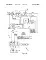
- FIG. 5is a block diagram illustrating an automatic output drive control arrangement of the present invention.
- FIG. 1is a diagram of a home telephone wire network 10 according to an embodiment of the invention, using existing residential wiring such as twisted pair telephone line wiring as network media.
- the network 10 supporting the Ethernet (IEEE 802.3) standardincludes network stations 12 a and 12 b that are connected to a twisted pair telephone line wiring 14 , via RJ-11 phone jacks 16 a and 16 b respectively.
- a telephone 18 connected to the RJ-11 phone jack 16 cmay continue to make phone calls while stations 12 a and 12 b are communicating.
- each network station 12for example a personal computer, printer, or intelligent consumer electronics device, includes a physical layer (PHY) transceiver 20 , a media access (MAC) layer 22 , and an operating system (OS) layer that performs higher layer function according to the OSI reference model.
- PHYphysical layer
- MACmedia access
- OSoperating system
- a home networking transceiver complying with the HPNA Specification 1.0may be used as the PHY transceiver 20 .
- the stations 12 a and 12 bcommunicate by transmitting band-limited pulses that carry network data modulated in the analog network signals.
- the physical layer transmittertransmits a band-limited pulse 5 , illustrated in FIG. 2A .
- the arrival position of a received pulseis detected using a waveform envelope 8 representing the absolute value 6 of the received signal, shown in FIG. 2B .
- the envelope 8is supplied to a slicing circuit described below, having a threshold level 9 selected to identify the arrival position 11 of the received pulse.
- the slicing circuitdetects the arrival position 11 of the pulse as an event representing a data pattern. This event can be used to recover a transmit clock and transmit data from the received signal.
- the received envelope waveformdepends largely on the wiring topology.
- the wiring topologymay cause multiple signal reflections, the shape of a received pulse may be so distorted that the envelope may have multiple localized maximum points.
- the wiring topology in the home networkis variable.
- the distortion of the received pulseis unpredictable, resulting in a waveform 26 as shown in FIG. 2C .
- the distorted waveform 26 of a received pulse signalhas multiple localized maximum and minimum points 26 a and 26 b due to wiring topology.
- FIG. 2Dillustrates the envelope waveform 28 of the distorted waveform 26 .
- FIG. 3is a block diagram of the physical layer transceiver 20 according to an embodiment of the present invention.
- the physical layer transceiver 20includes an input amplifier 30 connected to complementary input/output terminals TxRx_Pos and TxRx_Neg for amplifying analog network signals received from the telephone medium, such as the network signals shown in FIG. 2C .
- the physical layer transceiver 20also includes a signal conditioning circuit 32 that includes an envelope detection circuit 34 and an energy detection circuit 36 .
- the envelope detection circuit 34is responsive to the amplified received signal 26 to generate the envelope signal 28 .
- the envelope detector 34includes an absolute value circuit (e.g., a rectifier circuit) that generates an absolute value signal 39 representing the absolute value of the amplified received signal 26 , and a low pass filter coupled to the rectifier circuit for filtering out high-frequency components of the rectified signal, resulting in the envelope signal 28 .
- the envelope signal 28is output from the envelope detector 34 and supplied to the energy detector 36 .
- the energy detector 36includes an integrator that performs the mathematical process of integration of the envelope signal 28 over time to produce a signal proportional to energy of the received pulse signal.
- the physical layer transceiver 20also includes slicer circuits 38 a , 38 b , 38 c and 38 d , and a digital to analog (D/A) converter 40 for supplying analog threshold signals to the slicer circuits 38 .
- the physical layer transceiver 20also includes a digital controller 41 configured for controlling the digital analog converter 40 to output threshold signals supplied to the slicer circuits 38 .
- the digital controller 41is configured for controlling the threshold values applied to the slicers 38 a , 38 b , 38 c and 38 d based on the signals supplied by the slicers 38 to the digital controller 41 .
- slicer circuit 38 aoutputs a peak event signal indicating with respect to time whether the envelope signal 28 exceeds a peak threshold (P) supplied by the digital to analog converter 40 under the control of the digital controller 41 .
- Slicer circuits 38 b and 38 coutput data event signals and noise event signals indicating with respect to time whether the envelope signal 28 exceeds a data transition threshold (D) and a noise threshold (N), respectively.
- the slicer circuit 38 doutputs an energy event signal indicating with respect to time whether the energy signal output by energy detector 36 exceeds an energy threshold (E) supplied by the D/A converter 40 .
- the slicer circuits 38 a , 38 b , and 38 coutput peak, data transition, and noise event signals indicating, with respect to time whether the envelope signal 28 exceeds a peak threshold (P), a data transition threshold (D), and a noise threshold (N), respectively.
- Slicer 38 doutputs an energy event signal indicating with respect to time whether the energy signal from the energy detector 36 exceeds an energy threshold (E).
- the digital controller 41controls the noise, peak, data transition and energy thresholds based on the noise event signals and the peak event signals output by the slicers 38 c and 38 a , respectively, and produces a digital data signal based on the arrival position of the received pulse detected using either the energy event signal or the data event signal.
- the digital data signalis output to the media access controller 22 via a media independent interface (MII) 50 .
- MIImedia independent interface
- the physical layer transceiver 20also includes an output driver 52 (e.g., a current amplifier), that converts transmit data (TxD) produced by the digital controller 41 to an analog network signal supplied via the complementary input/output terminals TxRx_Pos and TxRx_Neg.
- the analog network signalis output at a selected one of 128 output gain values based on a 7-bit transmit gain (TxGain) signal output by the digital controller 41 .
- the physical layer transceiver 20comprises an output interface 42 including a Media-Independent Interface (MII) to general purpose serial interface (GPSI) converter 44 , management interface logic 46 , and buses 48 a and 48 b .
- the bus 48 atransfers transmit and receive data between the MAC 22 and the digital controller 41 in GPSI format.
- the converter 44converts the GPSI format data to nibble-wide data for transfer to the MAC 22 via the MII 50 .
- transmit data from the MAC 22 supplied via the MII 50is converted from nibble-wide data to GPSI format, and supplied to the digital controller 41 via the GPSI data bus 48 a.
- the output interface 42also includes a control data bus 48 b for transferring configuration data and status information between the digital converter 41 and the management interface logic 46 .
- the management interface logic 46is configured for storing at selected control registers 60 configuration data received from the MAC 22 via the MII 50 into the digital controller 41 .
- the threshold value E for the energy detector slicer circuit 38 dmay be supplied by the management agent via the MII 50 and set in the configuration registers 60 .
- the digital controller 41also comprises status registers 62 that include, for example, the threshold values for the threshold signals P, D, and E, and the 7-bit output amplifier gain control signal TxGain.
- the output interface 42also includes link detection logic 47 for determining whether a valid link is detected on the network medium 14 . If no valid access identification (AID) sequence is detected within three successive detection intervals, each having a preferred duration of about 800 milliseconds, the link status is sent to an invalid state. AID replaces the preamble conventionally used in 10 Base-T Ethernet (IEEE 802.3) systems. AID is a specific identifier, which is unique for each network station 12 . For example, AID may be a series of 8 pulses output from the PHY transceiver 20 of the transmitting station onto the telephone medium 14 , where the time intervals between the first pulse and the successive 7 pulses define respective values.
- a second pulseis output by the PHY transceiver 20 following a first pulse after time interval T 1 .
- T 1equals 66 clock cycles (assuming a 116 nanosecond clock)
- the corresponding valueis 00
- T 1equals 86, 106, or 126 clock cycles
- the valuesare 01, 10, or 11, respectively, where the maximum interval between pulses is 128 clock cycles.
- the same arrangementis used to detect the values representing time intervals T 2 , T 3 , T 4 , T 5 , T 6 and T 7 between the first pulse and each of the 6 pulses following the second pulse.
- the presence of the valid AIDcan be determined by detecting a first pulse, and detecting a presence of 7 successive pulses using detection windows having predetermined duration, for example, 128 clock cycles.
- FIG. 4that illustrates a sequence of envelope pulses 28 used to define an AID interval 90
- eight AID envelope pulses 28 a , 28 b , 28 c , 28 d , 28 e , 28 f , 28 g and 28 hare inserted before the data packet, which begins with the envelope pulse 28 i contiguously following the last AID envelope pulse 28 h .
- the envelope pulses 28are generated by the envelope detector 34 in response to received network signals 5 .
- the output characteristics of the physical layer transceiver 20such as the output drive level, substantially vary from run to run.
- the physical layer transceiver 20 of the present inventioncomprises an automatic output drive level control system 100 schematically shown in FIG. 5 .
- the system 100compares a level at the output of the transceiver 20 with a preset threshold level to produce a level control signal used to control the output level of the output driver 52 .
- the automatic output drive level control system 100may separately control output drive levels at the complementary input/output terminals TxRx_Pos and TxRx_Neg of the physical layer transceiver 20 .
- the terminals TxRx_Pos and TxRx_Negsupply complementary analog network signals transmitted to other network stations 12 .
- the automatic output drive level control system 100uses DC levels set at the terminals TxRx_Pos and TxRx_Neg to adjust the output drive level of the transceiver 20 to a proper value, such as the output drive voltage required by the HPNA specification 1.0.
- the automatic output drive level control system 100comprises a comparator circuit 102 for comparing DC levels set at the terminals TxRx_Pos and TxRx_Neg with a preset threshold level to produce a level control signal supplied to a drive control circuit 104 for controlling the output driver 52 .
- the digital controller 41may act as the drive control circuit 104 .
- the controlled input of the comparator circuit 102is connected to the output of a multiplexer 106 having a first input connected to the terminal TxRx_Pos, a second input coupled to the terminal TxRx_Neg, and a third input coupled to input amplification circuitry 108 of the transceiver 20 .
- the third input of the comparator circuit 102may be connected to the output of the envelope detector 34 .
- the slicer 38 a , 38 b or 38 cmay be used as the comparator circuit 102 .
- Fixed attenuators 110 and 112may be respectively connected between the terminals TxRx_Pos and TxRx_Neg and the corresponding inputs of the multiplexer 106 .
- the attenuators 110 and 112may provide attenuation with a ratio of 6.
- the multiplexer 106supplies the output of the input amplification circuitry 108 to the comparator circuit 102 for producing a peak event, data event, or noise event signal, depending on whether the slicer 38 a , 38 b or 38 c is used as the comparator circuit 102 .
- the drive control circuit 104controls the multiplexer 106 to pass a signal representing a DC level set at the terminal TxRx_Pos to the controlled input of the comparator circuit 102 .
- the comparator circuit 102compares the signal at its controlled input with a threshold level and produces a level control signal representing the difference between the compared signals.
- the level control signalis supplied to the drive control circuit 104 that controls the output driver 52 so as to reduce the level at the TxRx_Pos terminal if the signal at the controlled input of the comparator 102 is higher than the threshold level, or to increase the level at the TxRx_Pos terminal if the signal at the controlled input of the comparator 102 is lower than the threshold level.
- the control procedurecontinues until the signal at the controlled input of the comparator 102 becomes equal to the threshold level.
- the drive control circuit 104may increase or decrease the value of the gain control signal TxGain supplied to the output driver 52 until the signal at the controlled input of the comparator 102 is equal to the threshold level.
- the multiplexer 106is controlled to pass a signal representing a DC level set at the terminal TxRx_Neg to the controlled input of the comparator 102 .
- the drive control circuit 104controls the output driver 52 until the signal at the controlled input becomes equal to the threshold level.
- the output drive levelis adjusted for high and low power levels of the transciever 20 .
- an output drive level control proceduremay begin with setting a desired high power output level at the terminal TxRx_Pos or TxRx_Neg.
- the high power output level set at the corresponding terminal TxRx_Pos or TxRx_Negmay be a DC level, e.g. 2 V, corresponding to a high level of a sinusoidal transmit signal defined in the HPNA Specification 1.0.
- the DC levelis supplied to the controlled input of the comparator 102 for comparing with the threshold level.
- the drive control circuit 104adjusts the output drive level until the level at the controlled input becomes equal to the threshold level. Then, the output drive level at the corresponding terminal TxRx_Pos or TxRx_Neg may be adjusted for a desired low power output level.
- the low power output level set at the corresponding terminal TxRx_Pos or TxRx_Negmay be a DC level, e.g. 1 V, corresponding to a low level of the sinusoidal transmit signal defined in the HPNA Specification 1.0.
- the threshold valueis selected to provide the output drive level required by the HPNA Specification 1.0. As discussed above, the output drive level control procedure may be carried out for each of the terminals TxRx_Pos and TxRx_Neg.
Landscapes
- Engineering & Computer Science (AREA)
- Power Engineering (AREA)
- Computer Networks & Wireless Communication (AREA)
- Signal Processing (AREA)
- Dc Digital Transmission (AREA)
Abstract
Description
Claims (16)
Priority Applications (6)
| Application Number | Priority Date | Filing Date | Title |
|---|---|---|---|
| US09/413,821US8121180B1 (en) | 1999-10-07 | 1999-10-07 | Automatic output drive level control in home networking transceiver |
| JP2001530278AJP4636763B2 (en) | 1999-10-07 | 2000-05-16 | Automatic output drive level control in home networked transceivers |
| EP00935984AEP1221232B1 (en) | 1999-10-07 | 2000-05-16 | Automatic output drive level control in home networking transceiver |
| PCT/US2000/013387WO2001028175A1 (en) | 1999-10-07 | 2000-05-16 | Automatic output drive level control in home networking transceiver |
| DE60021743TDE60021743T2 (en) | 1999-10-07 | 2000-05-16 | Automatic output level control in transceiver for home network |
| KR1020027004461AKR100747125B1 (en) | 1999-10-07 | 2000-05-16 | Automatic Output Drive Level Control System in Home Networking Transceivers |
Applications Claiming Priority (1)
| Application Number | Priority Date | Filing Date | Title |
|---|---|---|---|
| US09/413,821US8121180B1 (en) | 1999-10-07 | 1999-10-07 | Automatic output drive level control in home networking transceiver |
Publications (1)
| Publication Number | Publication Date |
|---|---|
| US8121180B1true US8121180B1 (en) | 2012-02-21 |
Family
ID=23638788
Family Applications (1)
| Application Number | Title | Priority Date | Filing Date |
|---|---|---|---|
| US09/413,821Expired - Fee RelatedUS8121180B1 (en) | 1999-10-07 | 1999-10-07 | Automatic output drive level control in home networking transceiver |
Country Status (6)
| Country | Link |
|---|---|
| US (1) | US8121180B1 (en) |
| EP (1) | EP1221232B1 (en) |
| JP (1) | JP4636763B2 (en) |
| KR (1) | KR100747125B1 (en) |
| DE (1) | DE60021743T2 (en) |
| WO (1) | WO2001028175A1 (en) |
Families Citing this family (1)
| Publication number | Priority date | Publication date | Assignee | Title |
|---|---|---|---|---|
| JP2008219248A (en)* | 2007-03-01 | 2008-09-18 | Ic Plus Corp | Physical layer circuit |
Citations (27)
| Publication number | Priority date | Publication date | Assignee | Title |
|---|---|---|---|---|
| US3686634A (en)* | 1971-04-02 | 1972-08-22 | Esb Inc | Pulse rate monitor and indicator system utilizing a burst pulse counter and a pulse internal counter |
| US3958082A (en) | 1974-03-13 | 1976-05-18 | Nixdorf Computer Ag | Circuit arrangement for controlling of amplification devices in a semi-duplex data signal transmission system |
| GB2094105A (en)* | 1981-01-08 | 1982-09-08 | Itt Creed | Telegraph transmitter with line isolator |
| US4682050A (en)* | 1986-01-08 | 1987-07-21 | International Business Machines Corporation | Small signal swing driver circuit |
| US5041745A (en)* | 1990-10-01 | 1991-08-20 | General Signal Corporation | Failsafe bandpass filter/decoder |
| US5463329A (en)* | 1993-04-19 | 1995-10-31 | Canon Kabushiki Kaisha | Input circuit for level-shifting TTL or CMOS to ECL signals |
| US5467369A (en)* | 1990-02-15 | 1995-11-14 | Advanced Micro Devices, Inc. | AUI to twisted pair loopback |
| US5539771A (en)* | 1993-01-12 | 1996-07-23 | Hitachi, Ltd. | Communication line driver, LSI for interface including such a circuit and communication terminal apparatus |
| US5581197A (en)* | 1995-05-31 | 1996-12-03 | Hewlett-Packard Co. | Method of programming a desired source resistance for a driver stage |
| US5867097A (en)* | 1995-08-18 | 1999-02-02 | Samsung Electronics Co., Ltd. | Method and apparatus for alarm signal processing |
| US5890057A (en)* | 1996-11-27 | 1999-03-30 | Sierra Wireless, Inc. | Modulation signal calibration between modem and radio using loopback |
| US5917344A (en)* | 1996-02-13 | 1999-06-29 | Siemens Aktiengesellschaft | Driver circuit |
| US6208094B1 (en)* | 1999-03-17 | 2001-03-27 | National Semiconductor Corp. | Multiplexed video interface system |
| US6229466B1 (en)* | 1999-08-23 | 2001-05-08 | Level One Communications, Inc. | Digital calibration method and apparatus for multi-bit delta-sigma D/A converter |
| US6272325B1 (en)* | 1995-07-13 | 2001-08-07 | Globalstar L.P. | Method and apparatus for considering user terminal transmitted power during operation in a plurality of different communication systems |
| US6292015B1 (en)* | 1998-05-26 | 2001-09-18 | Mitsubishi Denki Kabushiki Kaisha | Semiconductor integrated circuit device including logic gate that attains reduction of power consumption and high-speed operation |
| US6377666B1 (en)* | 1998-10-29 | 2002-04-23 | Legerity | Apparatus and method for a PHY transmitter with programmable power mode control in CMOS |
| US6397287B1 (en)* | 1999-01-27 | 2002-05-28 | 3Com Corporation | Method and apparatus for dynamic bus request and burst-length control |
| US6408032B1 (en)* | 1998-09-30 | 2002-06-18 | Pmc-Sierra Ltd. | Transmit baseline wander correction technique |
| US6424630B1 (en)* | 1998-10-30 | 2002-07-23 | Advanced Micro Devices, Inc. | Apparatus and method for calibrating a home networking station receiving network signals on a telephone line medium |
| US6504634B1 (en)* | 1998-10-27 | 2003-01-07 | Air Fiber, Inc. | System and method for improved pointing accuracy |
| US6507223B2 (en)* | 2001-02-22 | 2003-01-14 | Sigmatel, Inc. | Differential line driver having adjustable common mode operation |
| US6526581B1 (en)* | 1999-08-03 | 2003-02-25 | Ucentric Holdings, Llc | Multi-service in-home network with an open interface |
| US6580905B1 (en)* | 1996-07-02 | 2003-06-17 | Ericsson Inc. | System and method for controlling the level of signals output to transmission media in a distributed antenna network |
| US6615301B1 (en)* | 1998-03-09 | 2003-09-02 | Samsung Electronics, Co., Ltd | Integrated data transceiver circuit for use with a serial bus and bus interface |
| US6711138B1 (en)* | 1999-09-30 | 2004-03-23 | Conexant Systems, Inc. | Digital subscriber line/home phoneline network router |
| US6748078B1 (en)* | 1998-12-18 | 2004-06-08 | Lucent Technologies Inc. | System and method for allocating overhead voltage in the transmission of pots and XDSL signals |
Family Cites Families (8)
| Publication number | Priority date | Publication date | Assignee | Title |
|---|---|---|---|---|
| JPS58190106A (en)* | 1982-04-30 | 1983-11-07 | Nec Corp | Power control circuit of transmission output |
| JPH0666715B2 (en)* | 1982-09-14 | 1994-08-24 | オムロン株式会社 | Power supply communication device |
| JPS62141823A (en)* | 1985-12-17 | 1987-06-25 | Fujitsu Ltd | Data transmission method |
| JPS62248306A (en)* | 1986-04-21 | 1987-10-29 | Mitsubishi Electric Corp | Output buffer circuit |
| JPH02177724A (en)* | 1988-12-28 | 1990-07-10 | Sumitomo Electric Ind Ltd | output buffer circuit |
| DE69032634T2 (en)* | 1989-06-27 | 1999-01-28 | Nec Corp., Tokio/Tokyo | Control circuit for the output waveform |
| JPH06113300A (en)* | 1992-09-28 | 1994-04-22 | Nec Corp | Bidirection catv transmission system |
| US6094441A (en)* | 1998-10-30 | 2000-07-25 | Advanced Micro Devices, Inc. | Apparatus and method for controlling transmission parameters of home network stations transmitting on a telephone line medium |
- 1999
- 1999-10-07USUS09/413,821patent/US8121180B1/ennot_activeExpired - Fee Related
- 2000
- 2000-05-16JPJP2001530278Apatent/JP4636763B2/ennot_activeExpired - Fee Related
- 2000-05-16DEDE60021743Tpatent/DE60021743T2/ennot_activeExpired - Lifetime
- 2000-05-16EPEP00935984Apatent/EP1221232B1/ennot_activeExpired - Lifetime
- 2000-05-16KRKR1020027004461Apatent/KR100747125B1/ennot_activeExpired - Fee Related
- 2000-05-16WOPCT/US2000/013387patent/WO2001028175A1/enactiveIP Right Grant
Patent Citations (27)
| Publication number | Priority date | Publication date | Assignee | Title |
|---|---|---|---|---|
| US3686634A (en)* | 1971-04-02 | 1972-08-22 | Esb Inc | Pulse rate monitor and indicator system utilizing a burst pulse counter and a pulse internal counter |
| US3958082A (en) | 1974-03-13 | 1976-05-18 | Nixdorf Computer Ag | Circuit arrangement for controlling of amplification devices in a semi-duplex data signal transmission system |
| GB2094105A (en)* | 1981-01-08 | 1982-09-08 | Itt Creed | Telegraph transmitter with line isolator |
| US4682050A (en)* | 1986-01-08 | 1987-07-21 | International Business Machines Corporation | Small signal swing driver circuit |
| US5467369A (en)* | 1990-02-15 | 1995-11-14 | Advanced Micro Devices, Inc. | AUI to twisted pair loopback |
| US5041745A (en)* | 1990-10-01 | 1991-08-20 | General Signal Corporation | Failsafe bandpass filter/decoder |
| US5539771A (en)* | 1993-01-12 | 1996-07-23 | Hitachi, Ltd. | Communication line driver, LSI for interface including such a circuit and communication terminal apparatus |
| US5463329A (en)* | 1993-04-19 | 1995-10-31 | Canon Kabushiki Kaisha | Input circuit for level-shifting TTL or CMOS to ECL signals |
| US5581197A (en)* | 1995-05-31 | 1996-12-03 | Hewlett-Packard Co. | Method of programming a desired source resistance for a driver stage |
| US6272325B1 (en)* | 1995-07-13 | 2001-08-07 | Globalstar L.P. | Method and apparatus for considering user terminal transmitted power during operation in a plurality of different communication systems |
| US5867097A (en)* | 1995-08-18 | 1999-02-02 | Samsung Electronics Co., Ltd. | Method and apparatus for alarm signal processing |
| US5917344A (en)* | 1996-02-13 | 1999-06-29 | Siemens Aktiengesellschaft | Driver circuit |
| US6580905B1 (en)* | 1996-07-02 | 2003-06-17 | Ericsson Inc. | System and method for controlling the level of signals output to transmission media in a distributed antenna network |
| US5890057A (en)* | 1996-11-27 | 1999-03-30 | Sierra Wireless, Inc. | Modulation signal calibration between modem and radio using loopback |
| US6615301B1 (en)* | 1998-03-09 | 2003-09-02 | Samsung Electronics, Co., Ltd | Integrated data transceiver circuit for use with a serial bus and bus interface |
| US6292015B1 (en)* | 1998-05-26 | 2001-09-18 | Mitsubishi Denki Kabushiki Kaisha | Semiconductor integrated circuit device including logic gate that attains reduction of power consumption and high-speed operation |
| US6408032B1 (en)* | 1998-09-30 | 2002-06-18 | Pmc-Sierra Ltd. | Transmit baseline wander correction technique |
| US6504634B1 (en)* | 1998-10-27 | 2003-01-07 | Air Fiber, Inc. | System and method for improved pointing accuracy |
| US6377666B1 (en)* | 1998-10-29 | 2002-04-23 | Legerity | Apparatus and method for a PHY transmitter with programmable power mode control in CMOS |
| US6424630B1 (en)* | 1998-10-30 | 2002-07-23 | Advanced Micro Devices, Inc. | Apparatus and method for calibrating a home networking station receiving network signals on a telephone line medium |
| US6748078B1 (en)* | 1998-12-18 | 2004-06-08 | Lucent Technologies Inc. | System and method for allocating overhead voltage in the transmission of pots and XDSL signals |
| US6397287B1 (en)* | 1999-01-27 | 2002-05-28 | 3Com Corporation | Method and apparatus for dynamic bus request and burst-length control |
| US6208094B1 (en)* | 1999-03-17 | 2001-03-27 | National Semiconductor Corp. | Multiplexed video interface system |
| US6526581B1 (en)* | 1999-08-03 | 2003-02-25 | Ucentric Holdings, Llc | Multi-service in-home network with an open interface |
| US6229466B1 (en)* | 1999-08-23 | 2001-05-08 | Level One Communications, Inc. | Digital calibration method and apparatus for multi-bit delta-sigma D/A converter |
| US6711138B1 (en)* | 1999-09-30 | 2004-03-23 | Conexant Systems, Inc. | Digital subscriber line/home phoneline network router |
| US6507223B2 (en)* | 2001-02-22 | 2003-01-14 | Sigmatel, Inc. | Differential line driver having adjustable common mode operation |
Also Published As
| Publication number | Publication date |
|---|---|
| DE60021743D1 (en) | 2005-09-08 |
| JP4636763B2 (en) | 2011-02-23 |
| DE60021743T2 (en) | 2006-04-20 |
| JP2003511978A (en) | 2003-03-25 |
| KR100747125B1 (en) | 2007-08-09 |
| WO2001028175A1 (en) | 2001-04-19 |
| EP1221232A1 (en) | 2002-07-10 |
| KR20020041817A (en) | 2002-06-03 |
| EP1221232B1 (en) | 2005-08-03 |
Similar Documents
| Publication | Publication Date | Title |
|---|---|---|
| US6819760B1 (en) | Adaptive energy detector gain control in physical layer transceiver for home telephone wire network | |
| US6094441A (en) | Apparatus and method for controlling transmission parameters of home network stations transmitting on a telephone line medium | |
| US6421735B1 (en) | Apparatus and method for automatically selecting a network port for a home network station | |
| US6097732A (en) | Apparatus and method for controlling transmission parameters of selected home network stations transmitting on a telephone medium | |
| US6771750B1 (en) | Physical layer transceiver architecture for a home network station connected to a telephone line medium | |
| US5963539A (en) | Method and apparatus for detecting collisions on a network | |
| US6424630B1 (en) | Apparatus and method for calibrating a home networking station receiving network signals on a telephone line medium | |
| US6735217B1 (en) | Method and apparatus for detecting collisions on a network using multi-cycle waveform pulses | |
| US7215763B1 (en) | Self-calibration procedure in physical layer transceiver for home telephone wire network | |
| EP0966128B1 (en) | Apparatus and method of determining a link status between network stations connected to a telephone line medium | |
| AU3673601A (en) | Method to establish a home network in multiple physical layers | |
| US6909725B1 (en) | Implementation of HPNA 2.0 network states in hardware | |
| US6438184B1 (en) | Apparatus and method for adjusting an input gain and comparator threshold value within an access identifier interval on a telephone line medium | |
| US8208520B2 (en) | Variable state length initialization | |
| US8121180B1 (en) | Automatic output drive level control in home networking transceiver | |
| WO2001071999A1 (en) | Device and method for adjusting input gain for multiple signal formats in a data network | |
| US6668032B1 (en) | Device and method for signal sampling at multiple clock rates | |
| JP2000013283A (en) | Signal transmission device and method thereof | |
| CN102326435B (en) | Communication equipment and method, the gateway comprising this equipment, device and system | |
| US6967967B1 (en) | Home network transmission deferral | |
| JP2004088576A (en) | Digital signal transmission equipment |
Legal Events
| Date | Code | Title | Description |
|---|---|---|---|
| AS | Assignment | Owner name:ADVANCED MICRO DEVICES, INC., CALIFORNIA Free format text:ASSIGNMENT OF ASSIGNORS INTEREST;ASSIGNOR:KELLER, PHILIP;REEL/FRAME:010302/0514 Effective date:19991005 | |
| AS | Assignment | Owner name:GLOBALFOUNDRIES INC., CAYMAN ISLANDS Free format text:AFFIRMATION OF PATENT ASSIGNMENT;ASSIGNOR:ADVANCED MICRO DEVICES, INC.;REEL/FRAME:023120/0426 Effective date:20090630 | |
| ZAAA | Notice of allowance and fees due | Free format text:ORIGINAL CODE: NOA | |
| ZAAB | Notice of allowance mailed | Free format text:ORIGINAL CODE: MN/=. | |
| STCF | Information on status: patent grant | Free format text:PATENTED CASE | |
| FPAY | Fee payment | Year of fee payment:4 | |
| AS | Assignment | Owner name:WILMINGTON TRUST, NATIONAL ASSOCIATION, DELAWARE Free format text:SECURITY AGREEMENT;ASSIGNOR:GLOBALFOUNDRIES INC.;REEL/FRAME:049490/0001 Effective date:20181127 | |
| MAFP | Maintenance fee payment | Free format text:PAYMENT OF MAINTENANCE FEE, 8TH YEAR, LARGE ENTITY (ORIGINAL EVENT CODE: M1552); ENTITY STATUS OF PATENT OWNER: LARGE ENTITY Year of fee payment:8 | |
| AS | Assignment | Owner name:GLOBALFOUNDRIES U.S. INC., CALIFORNIA Free format text:ASSIGNMENT OF ASSIGNORS INTEREST;ASSIGNOR:GLOBALFOUNDRIES INC.;REEL/FRAME:054633/0001 Effective date:20201022 | |
| AS | Assignment | Owner name:GLOBALFOUNDRIES INC., CAYMAN ISLANDS Free format text:RELEASE BY SECURED PARTY;ASSIGNOR:WILMINGTON TRUST, NATIONAL ASSOCIATION;REEL/FRAME:054636/0001 Effective date:20201117 | |
| AS | Assignment | Owner name:GLOBALFOUNDRIES U.S. INC., NEW YORK Free format text:RELEASE BY SECURED PARTY;ASSIGNOR:WILMINGTON TRUST, NATIONAL ASSOCIATION;REEL/FRAME:056987/0001 Effective date:20201117 | |
| FEPP | Fee payment procedure | Free format text:MAINTENANCE FEE REMINDER MAILED (ORIGINAL EVENT CODE: REM.); ENTITY STATUS OF PATENT OWNER: LARGE ENTITY | |
| LAPS | Lapse for failure to pay maintenance fees | Free format text:PATENT EXPIRED FOR FAILURE TO PAY MAINTENANCE FEES (ORIGINAL EVENT CODE: EXP.); ENTITY STATUS OF PATENT OWNER: LARGE ENTITY | |
| STCH | Information on status: patent discontinuation | Free format text:PATENT EXPIRED DUE TO NONPAYMENT OF MAINTENANCE FEES UNDER 37 CFR 1.362 | |
| FP | Lapsed due to failure to pay maintenance fee | Effective date:20240221 |