US8120975B2 - Memory having negative voltage write assist circuit and method therefor - Google Patents
Memory having negative voltage write assist circuit and method thereforDownload PDFInfo
- Publication number
- US8120975B2 US8120975B2US12/361,826US36182609AUS8120975B2US 8120975 B2US8120975 B2US 8120975B2US 36182609 AUS36182609 AUS 36182609AUS 8120975 B2US8120975 B2US 8120975B2
- Authority
- US
- United States
- Prior art keywords
- bit line
- column
- potential
- memory
- applying
- Prior art date
- Legal status (The legal status is an assumption and is not a legal conclusion. Google has not performed a legal analysis and makes no representation as to the accuracy of the status listed.)
- Active, expires
Links
Images

Classifications
- G—PHYSICS
- G11—INFORMATION STORAGE
- G11C—STATIC STORES
- G11C11/00—Digital stores characterised by the use of particular electric or magnetic storage elements; Storage elements therefor
- G11C11/21—Digital stores characterised by the use of particular electric or magnetic storage elements; Storage elements therefor using electric elements
- G11C11/34—Digital stores characterised by the use of particular electric or magnetic storage elements; Storage elements therefor using electric elements using semiconductor devices
- G11C11/40—Digital stores characterised by the use of particular electric or magnetic storage elements; Storage elements therefor using electric elements using semiconductor devices using transistors
- G11C11/41—Digital stores characterised by the use of particular electric or magnetic storage elements; Storage elements therefor using electric elements using semiconductor devices using transistors forming static cells with positive feedback, i.e. cells not needing refreshing or charge regeneration, e.g. bistable multivibrator or Schmitt trigger
- G11C11/413—Auxiliary circuits, e.g. for addressing, decoding, driving, writing, sensing, timing or power reduction
- G11C11/417—Auxiliary circuits, e.g. for addressing, decoding, driving, writing, sensing, timing or power reduction for memory cells of the field-effect type
- G11C11/419—Read-write [R-W] circuits
Definitions
- This disclosurerelates generally to memories, and more specifically, to a memory having a negative voltage write assist circuit and method therefor.
- Static random access memoriesare generally used in applications requiring high speed, such as memory in a data processing system.
- Each SRAM cellstores one bit of data and is implemented as a pair of cross-coupled inverters.
- the SRAM cellis only stable in one of two possible voltage levels.
- the logic state of the cellis determined by whichever of the two inverter outputs is a logic high, and can be made to change states by applying a voltage of sufficient magnitude and duration to the appropriate cell input.
- the stability of a SRAM cellis an important issue.
- the SRAM cellmust be stable against transients, process variations, soft error, and power supply fluctuations which may cause the cell to inadvertently change logic states. Also, the SRAM cell must provide good stability during read operations without harming speed or the ability to write to the cell.
- good read stabilitycan make it difficult to write to the memory cells.
- process variationscan cause some cells of the array to be more difficult to write than others.
- One way to have both good write performance and good read stabilityis to lower the memory array power supply voltage for write operations and raise the memory array power supply voltage for read operations.
- the write performancecan be improved further by lowering the logic low bit line voltage below ground during the write operation.
- a capacitor bootstrapping circuitis used to boost the bit line voltage negative.
- a bootstrap circuitrequires the use of a write driver circuit with relatively large transistors. Also, the ratio of capacitance between the bit line and the bootstrapping circuit is difficult to trim for different voltages.
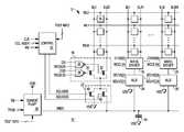
- FIG. 1illustrates, in block diagram form, an integrated circuit memory in accordance with an embodiment.
- FIG. 2illustrates a timing diagram of various signals of the memory of FIG. 1 during a write operation.
- an integrated circuit memoryhaving a circuit to boost a bit line voltage to below ground level during a write operation.
- the circuitincludes a charge pump, a multiplexing circuit, and a capacitor.
- the charge pumpgenerates a negative voltage and continually charges or maintains a predetermined voltage level on the capacitor.
- the multiplexerreceives non-overlapping control signals to cause the bit line to be first pulled to ground, or some other predetermined voltage level, and then to a negative voltage, for example, 200 millivolts (mV).
- the capacitoris coupled to store negative charge to assist in boosting the bit line voltage below ground.
- the memoryis a static random access memory (SRAM).
- the memory arrayis first tested for memory cells that are relatively more difficult to write at a predetermined power supply voltage.
- the locations of those cellsare stored, and only those cells receive the negative bit line boost during a write operation.
- charge pumpscan be implemented for each subarray and individually trimmed so that the negative boost voltage is adjusted on a subarray basis.
- a method of writing data in a memorycomprising: selecting a first column for writing; initiating the writing by applying a logic high to a first bit line of the first column and a first potential to a second bit line of the first column that is lower than the logic high; providing a second potential that is lower than the first potential; and removing the first potential and applying the second potential to the second bit line.
- the step of initiating the writingmay be further characterized by the subarray being powered by a voltage differential no less than a difference between the logic high and the first potential.
- the step of initiating the writingmay be further characterized by the first potential being ground.
- the methodmay further comprise a step of returning the first and second bit line to a common voltage.
- the methodmay further comprise: enabling a word line that intersects the first column prior to the step of removing; and disabling the word line prior to the step of returning.
- the methodmay further comprise: selecting a second column for writing; applying the logic high to a first bit line of the second column and the first potential to a second bit line of the second column; and returning the first and second bit lines of the second column to the common voltage without lowering the second bit line below the first potential.
- the methodmay further comprise: testing the first and second columns for weak bits for writing; identifying a weak bit for writing in the first column; and finding no weak bits for writing in the second column.
- the following stepsmay occur simultaneously: initiating the writing by applying a logic high to a first bit line of the first column and a first potential to a second bit line of the first column; and applying the logic high to a first bit line of the second column and the first potential to a second bit line of the second column.
- the step of initiating the writing by applying a logic high to a first bit line of the first column and a first potential to a second bit line of the first columnmay occur before the step of applying the logic high to a first bit line of the second column and the first potential to a second bit line of the second column.
- the step of removing the first potential and applying a second potential to the second bit linemay be further characterized by the second potential varying at least 10 millivolt during its application to the second bit line.
- a memorycomprising: a subarray having columns, wherein each column has a pair of bit lines; a first write driver for maintaining a logic high at a first selected bit line of a first selected pair of bit lines and providing a logic low to a second selected bit line of the first selected pair of bit lines by coupling a negative power supply node to the second selected bit line; a charge pump for providing an output at a negative voltage; a first multiplexer having a first input coupled to the output of the charge pump, a second input coupled to a low power supply terminal for receiving a low voltage that is greater than the negative voltage, and an output coupled to the negative power supply node.
- the low voltagemay be ground potential, and a capacitor may be coupled between a node at a predetermined potential, such as ground potential, and the output of the charge pump. Alternatively, the capacitor may be coupled between the output of the charge pump and a node that is at a potential different from ground potential.
- the first write drivermay provide the logic high to the first selected bit line based upon a logic state of a data input signal received by the first write driver.
- a controllermay be coupled to the first multiplexer that directs the first multiplexer to couple the low power supply terminal to the first write driver during an initial portion of a write cycle and directs the first multiplexer to couple the output of the charge pump to the first write driver after the initial portion of the write cycle.
- a controllermay be coupled to the first multiplexer that directs the first multiplexer to couple the low power supply terminal to the negative power supply node during an initial portion of a write cycle and determines if the first multiplexer should couple the output of the charge pump to the negative power supply node after the initial portion of the write cycle or if the first multiplexer should continue coupling the low power supply terminal to the negative power supply node during all of the write cycle.
- the controllermay be further characterized as receiving test information that indicates which of the columns in the subarray are to be written with one of its bit lines coupled to the output of the charge pump.
- the memorymay further comprise: a second write driver for maintaining a logic high to a first selected bit line of a second selected pair of bit lines and providing a logic low to a second selected bit line of the second selected pair of bit lines by coupling a second negative power supply node to the second selected bit line of the second selected pair of bit lines; and a second multiplexer having a first input coupled to the output of the charge pump, a second input coupled to a low power supply terminal for receiving a low voltage that is greater than the negative voltage, and an output coupled to the second negative power supply node.
- a methodcomprising: providing a memory having a subarray having a plurality of columns, wherein each column of the plurality of columns has a pair of bit lines; writing data to a bitcell in a first selected column of the plurality of columns by enabling a word line that is coupled to the bitcell and applying a logic high to a first bit line of the first selected column and a logic low to a second bit line of the first selected column, wherein the step of applying the logic low comprises: applying a first potential to the second bit line that is a lower voltage than the logic high for an initial portion of a first write cycle; providing a negative voltage; and applying the negative voltage to the second bit line during a subsequent portion of the first write cycle.
- the methodmay further comprise: writing data to a bitcell in a second selected column of the plurality of columns by enabling a word line that is coupled to the bitcell and applying a logic high to a first bit line of the second selected column and a logic low to a second bit line of the second selected column, wherein the step of applying the logic low to the second bit line of the second selected column comprises: applying the first potential to the second bit line of the second selected column from a beginning of a second write cycle to an end of the second write cycle; and applying a common voltage to the first and second bit lines of the second selected column after the step of applying the first potential to the second bit line of the second selected column.
- the step of providing a memorymay be further characterized by the first selected column having a bitcell that is weak for writing.
- Using a charge pump to generate a relatively constant negative write assist voltage instead of a bootstrap circuiteliminates the need for very large write driver transistors. Also, the output voltage of the charge pump is more easily trimmed than the voltage provided by the bootstrap circuit because the charge pump output level is not as dependent on a capacitance ratio.
- the semiconductor substrate described hereincan be any semiconductor material or combinations of materials, such as gallium arsenide, silicon germanium, silicon-on-insulator (SOI), silicon, monocrystalline silicon, the like, and combinations of the above.
- SOIsilicon-on-insulator
- assertor “set” and “negate” (or “deassert” or “clear”) are used herein when referring to the rendering of a signal, status bit, or similar apparatus into its logically true or logically false state, respectively. If the logically true state is a logic level one, the logically false state is a logic level zero. And if the logically true state is a logic level zero, the logically false state is a logic level one.
- Each signal described hereinmay be designed as positive or negative logic, where negative logic can be indicated by a bar over the signal name or a letter “B” following the name.
- negative logicthe signal is active low where the logically true state corresponds to a logic level zero.
- positive logicthe signal is active high where the logically true state corresponds to a logic level one.
- any of the signals described hereincan be designed as either negative or positive logic signals. Therefore, in alternate embodiments, those signals described as positive logic signals may be implemented as negative logic signals, and those signals described as negative logic signals may be implemented as positive logic signals.
- FIG. 1illustrates, in block diagram form, an integrated circuit memory 10 in accordance with an embodiment.
- memory 10is an embedded SRAM in a data processing system including a processor, microcontroller, or the like.
- memory 10may be a different type of memory or a “standalone” memory.
- Integrated circuit memory 10includes memory array 12 , a plurality of write drivers including write drivers 16 , 18 , and 20 , a plurality of multiplexing circuits including multiplexing circuits 22 , 24 , and 26 , charge pump 28 , and control circuit 30 .
- Memory array 12includes a plurality of memory cells, such as memory cell 14 organized in M+1 rows and N+1 columns, where M and N can be any integer.
- a column of memory cellsincludes a bit line pair and all of the memory cells connected to the bit line pair.
- bit line pair BL 0 /BLB 0 and the memory cells coupled to bit line pair BL 0 /BLB 0such as memory cell 14
- bit line pairs BL 1 /BLB 1 and BLN/BLBN, with their respective memory cellseach comprise a column.
- a row of memory cellsincludes a word line and all of the memory cells connected to the word line.
- word line WL 0 and the memory cells coupled theretocomprises a row.
- word lines WL 1 and WLM and the memory cells coupled theretoeach comprises a row.
- Memory cell 14is at the intersection of a column having bit line pair BL 0 /BLB 0 and a row having word line WL 0 .
- Write driver 16includes N-channel transistors 32 and 34 and NOR logic gates 36 and 38 .
- the other write drivers, such as write drivers 18 and 20are identical to write driver 16 .
- Multiplexer circuit 22includes N-channel transistors 40 and 42 .
- the other multiplexer circuits, such as multiplexer circuits 24 and 26are identical to multiplexer circuit 22 .
- Each of the memory cells of array 12are six-transistor SRAM cells.
- Memory array 12may be one memory array of a plurality of memory arrays. Each of the memory cells of array 12 receives a power supply voltage equal to about VDD, or 0.9 volts. In other embodiments, the SRAM cells may have a different number of transistors and receive a different power supply voltage. Alternatively, the memory cells may be 8-transistor register-file cells instead of 6-transistor SRAM cells.
- N-channel transistor 32has a first current electrode (drain/source) coupled to bit line BLB 0 , a control electrode (gate), and a second current electrode (drain/source).
- N-channel transistor 34has a first current electrode coupled to bit line BL 0 , a control electrode, and a second current electrode coupled to the second current electrode of transistor 32 .
- NOR logic gate 36has a first input for receiving an input data signal labeled “DI 0 ”, a second input for receiving write column address WCOLB 0 , and an output coupled to the control electrode of transistor 32 .
- NOR logic gate 38has a first input for receiving an input data signal labeled “DIB 0 ”, a second input for receiving write column address WCOLB 0 , and an output coupled to the control electrode of transistor 34 .
- Write drivers 18 and 20are the same as write driver 16 except that the received data and address signals are different.
- N-channel transistor 40has a first current electrode coupled to the second current electrodes of transistors 32 and 34 , a control electrode for receiving a select signal labeled “SELVSS 0 ”, and a second current electrode coupled to receive a power supply voltage labeled “VSS”.
- VSSis coupled to ground. In another embodiment, VSS may be coupled to receive a different power supply voltage.
- N-channel transistor 42has a first current electrode coupled to the second current electrodes of transistors 32 and 34 , a control electrode for receiving a select signal labeled “SELNEG 0 ”, and a second current electrode coupled to receive a negative voltage labeled “VNEG”.
- Multiplexer 24is the same as multiplexer 22 except that the control gates of multiplexer 24 receive different, decoded, select signals labeled “SELVSS 1 ” and “SELNEG 1 ”. Also, multiplexer 26 is the same as multiplexer 22 except that the control gates of multiplexer 26 receive select signals labeled “SELVSSN” and “SELNEGN”.
- Control circuit 30has a first input for receiving a clock signal labeled “CLK”, a second input for receiving a plurality of column address signals labeled “COL ADDR”, a third input for receiving a write enable signal labeled “WE”, a fourth input for receiving test information labeled “TEST INFO”, a plurality of outputs for providing decoded select signals including a first output for providing a select signal labeled “SELVSS 0 ”, and a second output for providing a select signal labeled “SELNEG 0 ”.
- control circuit 30directs the multiplexer to first couple VSS to a selected column having a weak cell, decouple VSS from the selected column, and then couple VNEG to the selected column.
- Control circuit 30can be shared across multiple columns in memory array 12 . Alternatively, control circuit 30 can be implemented on a column-by-column basis for each column in memory array 12 .
- a word line driver block(not shown) is coupled to all of the word lines of memory array 12 , such as word lines labeled WL 0 , WL 1 , and WLM, and in response to a row address, provides a word line voltage to select a row.
- a column addressselects a bit line pair for a read or a write operation.
- Write drivers 16 , 18 , and 20are coupled to a bit line pair and function to couple a bit line pair to receive an input data signal labeled, for example, “DI 0 ” and “DIB 0 ”.
- the write driversalso receive a write column select signal labeled, for example, “WCOLB 0 ”, “WCOLB 1 ”, and “WCOLBN” and selects which bit line pair will receive input data. Note that the write column select signals are active low signals. Column logic circuits, such as column decoders, precharge and equalization circuits, bit line loads, sense amplifiers, and the like are not illustrated for the purposes of clarity and simplicity.
- Charge pump 28has a first input for receiving an enable signal labeled “EN”, one or more trim signals labeled “TRIM”, a third input for receiving signals TEST INFO, a fourth input for receiving a power supply voltage labeled “VDD”, and an output for providing a negative voltage labeled “VNEG”.
- Charge pump 28is a conventional charge pump for boosting a received voltage to a different voltage. In the illustrated embodiment, charge pump 28 receives a positive power supply voltage, for example, 0.9 volts, and provides a negative output voltage of, for example, ⁇ 200 millivolts (mV). During operation, charge pump 28 provides a relatively constant negative voltage to maintain charge on capacitor 44 .
- the negative voltageis used to decrease the voltage of a select bit line to below ground to assist a selected memory cell to change logic states.
- the charge pumpcan be any type of charge pump, multi-stage or single-stage, that will maintain a negative voltage at its output.
- write driver 16will receive input data signals DI 0 /DIB 0 to be stored in a predetermined location in memory array 12 .
- the bit line pairs of the memory arrayare typically precharged and equalized to a common voltage near the positive power supply voltage.
- a write enable signal WEis asserted as a logic high to control 30 .
- a row and column addressis provided to select a memory cell, for example, memory cell 14 .
- the complementary data signals DI 0 /DIB 0are provided to bit line pair BL 0 /BLB 0 to initiate writing to cell 14 .
- the column select signals WCOLB 0causes the data signals DI 0 /DIB 0 to be coupled to the selected bit line pair and thus to the selected memory cell.
- a complementary voltage on the bit line paircauses a logic state of the storage nodes of the selected memory cell to change state, if necessary. For example, in the case where a logic one is written to bit line pair BL 0 /BLB 0 , data signal DI 0 will be a logic high potential and data signal DIB 0 will be a logic low potential.
- the logic low data signal DIB 0 and the logic low signal WCOLB 0 of write driver 16will cause NOR logic gate 38 to output a logic high, thus making transistor 34 conductive.
- Transistor 32will be substantially non-conductive allowing bit line BLB 0 to remain at a logic high voltage.
- Select signal SELVSS 0will cause transistor 40 to be conductive, providing a path to VSS (ground) and causing bit line BL 0 to be pulled low to about VSS. If memory cell 14 is predetermined to require a negative bit line voltage for write assistance, then a predetermined time after signal SELVSS 0 is asserted, signal SELNEG 0 will be asserted causing transistor 42 to become conductive.
- Signal SELVSS 0will be deasserted, or negated, before signal SELNEG 0 is asserted.
- Bit line BL 0will be pulled negative making it easier for the storage nodes of memory cell 14 to change state, if necessary, to store the new state.
- Signals SELVSS 0 and SELNEG 0are non-overlapping signals to prevent the negative voltage VNEG from being coupled to VSS any time during operation. After the write operation, the word line is deselected and both bit lines of the bit line pair are returned to the precharge potential.
- the ability to write to the memory cellsis improved by boosting the voltage on the bit line negative, or below ground potential.
- the generation of a negative voltage using a charge pumpconsumes extra power. Hence, it is desirable to use a negative bit line voltage only if needed.
- bit line voltageis boosted at the correct time.
- the bit line voltageis pulled to ground and then boosted negative.
- the bit line voltagemay be pulled to a different voltage before boosting negative.
- Charge pump 28is enabled during normal operation if it is determined that a negative write assist voltage is needed. Alternately, charge pump 28 may always be enabled.
- An enable signal ENis provided to allow charge pump 28 to be disabled for, for example, memory testing.
- the negative output VNEGmay be adjusted to provide a different negative output voltage using signal TRIM.
- the test resultsmay be stored in registers, non-volatile memory, or the like, and may be used to determine whether or not to enable charge pump 28 , what the negative output voltage should be, and which cells are weak and need to be assisted during write operations.
- Memory array 12may be first tested without enabling charge pump 28 . If the memory fails, then charge pump 28 may be enabled and memory array 12 tested with different values of VNEG. If no weak bits are found in memory array 12 , then charge pump 28 may not be enabled for operation.
- the TEST INFO inputscan be used to specify operation of charge pump 28 during functional operation of memory array 12 .
- FIG. 2illustrates a timing diagram of various signals of the memory of FIG. 1 during a write operation.
- memory cell 14is being written and a column address is provided that selects bit lines BL 0 /BLB 0 .
- Complementary data in signals DI 0 /DIB 0are provided to write driver 16 along with a write column select signal (see FIG. 1 ). Note that the cross-hatching indicates that data in signals DI 0 /DIB 0 are invalid during that time period.
- Multiplexer signal SELVSS 0is a logic high, causing transistor 40 to be conductive.
- One of transistors 32 or 34is made conductive by the state of the data in signals DI 0 /DIB 0 , coupling one of the bit lines to VSS, or ground in the illustrated embodiment.
- signal SELVSS 0is negated, causing transistor 40 to become substantially non-conductive.
- signal SELNEG 0is asserted as a logic high, causing transistor 42 to become conductive.
- the selected logic low bit lineis boosted negative.
- VNEGis provided at ⁇ 200 mV. However, as can be seen after time T 2 , the voltage of VNEG is increased, or approaches VSS, because of charge sharing between the bit lines and capacitor 44 .
- VNEGis increased by 20 mV to ⁇ 180 mV.
- voltage VNEGmay vary by at least 10 millivolts. How much VNEG increases depends on the relative capacitance of capacitor 44 to the total bit line capacitance that is electrically connected to VNEG.
- the boosted bit line voltagemay be different.
- the bit line voltagebegins to separate in response to the data in signals and the logic low bit line is first pulled to about VSS potential at time T 2 . At time T 2 , the bit line is coupled to VNEG, causing a bit line to be pulled negative after time T 2 .
- signal SELNEG 0is negated, causing transistor 42 to be substantially non-conductive.
- signal SELVSS 0is reasserted, causing transistor 40 to be conductive in preparation for the next write operation and the bit lines are precharged.
- the write operationrequired about one half of a cycle of clock signal CLK.
- the write operationmay require a different time period.
- the logic low data lineis boosted below ground. In other embodiments, the boosted voltage level may be different.
- FIG. 1 and the discussion thereofdescribe an exemplary information processing architecture
- this exemplary architectureis presented merely to provide a useful reference in discussing various aspects of the invention.
- the description of the architecturehas been simplified for purposes of discussion, and it is just one of many different types of appropriate architectures that may be used in accordance with the invention.
- Those skilled in the artwill recognize that the boundaries between logic blocks are merely illustrative and that alternative embodiments may merge logic blocks or circuit elements or impose an alternate decomposition of functionality upon various logic blocks or circuit elements.
- circuits depicted hereinare merely exemplary, and that in fact many other circuits can be implemented which achieve the same functionality.
- any arrangement of components to achieve the same functionalityis effectively “associated” such that the desired functionality is achieved.
- any two components herein combined to achieve a particular functionalitycan be seen as “associated with” each other such that the desired functionality is achieved, irrespective of circuits or intermedial components.
- any two components so associatedcan also be viewed as being “operably connected,” or “operably coupled,” to each other to achieve the desired functionality.
- integrated circuit memory 10are circuitry located on a single integrated circuit or within a same device.
- integrated circuit memory 10may include any number of separate integrated circuits or separate devices interconnected with each other.
- charge pump 28may be located on a same integrated circuit memory array 12 or on a separate integrated circuit separate from other elements of memory 10 . Also, charge pump 28 may also be shared by multiple memory arrays 12 .
- Coupledis not intended to be limited to a direct coupling or a mechanical coupling.
Landscapes
- Engineering & Computer Science (AREA)
- Microelectronics & Electronic Packaging (AREA)
- Computer Hardware Design (AREA)
- Static Random-Access Memory (AREA)
Abstract
Description
Claims (20)
Priority Applications (5)
| Application Number | Priority Date | Filing Date | Title |
|---|---|---|---|
| US12/361,826US8120975B2 (en) | 2009-01-29 | 2009-01-29 | Memory having negative voltage write assist circuit and method therefor |
| TW098145618ATWI506625B (en) | 2009-01-29 | 2009-12-29 | Memory having negative voltage write assist circuit and method therefor |
| PCT/US2010/020852WO2010088042A2 (en) | 2009-01-29 | 2010-01-13 | Memory having negative voltage write assist circuit and method therefor |
| CN201080005845.XACN102301424B (en) | 2009-01-29 | 2010-01-13 | Memory having negative voltage write assist circuit and method therefor |
| JP2011548022AJP5473019B2 (en) | 2009-01-29 | 2010-01-13 | MEMORY HAVING NEGATIVE VOLTAGE WRITE SUPPORT CIRCUIT AND METHOD THEREOF |
Applications Claiming Priority (1)
| Application Number | Priority Date | Filing Date | Title |
|---|---|---|---|
| US12/361,826US8120975B2 (en) | 2009-01-29 | 2009-01-29 | Memory having negative voltage write assist circuit and method therefor |
Publications (2)
| Publication Number | Publication Date |
|---|---|
| US20100188909A1 US20100188909A1 (en) | 2010-07-29 |
| US8120975B2true US8120975B2 (en) | 2012-02-21 |
Family
ID=42354042
Family Applications (1)
| Application Number | Title | Priority Date | Filing Date |
|---|---|---|---|
| US12/361,826Active2029-08-14US8120975B2 (en) | 2009-01-29 | 2009-01-29 | Memory having negative voltage write assist circuit and method therefor |
Country Status (5)
| Country | Link |
|---|---|
| US (1) | US8120975B2 (en) |
| JP (1) | JP5473019B2 (en) |
| CN (1) | CN102301424B (en) |
| TW (1) | TWI506625B (en) |
| WO (1) | WO2010088042A2 (en) |
Cited By (18)
| Publication number | Priority date | Publication date | Assignee | Title |
|---|---|---|---|---|
| US8964490B2 (en) | 2013-02-07 | 2015-02-24 | Apple Inc. | Write driver circuit with low voltage bootstrapping for write assist |
| US20150213880A1 (en)* | 2014-01-24 | 2015-07-30 | Taiwan Semiconductor Manufacturing Company, Ltd. | Writing data to a memory cell |
| US9202555B2 (en) | 2012-10-19 | 2015-12-01 | Qualcomm Incorporated | Write word-line assist circuitry for a byte-writeable memory |
| US20160293248A1 (en)* | 2015-03-30 | 2016-10-06 | Taiwan Semiconductor Manufacturing Company, Ltd. | Static random access memory and method of operating the same |
| US9548104B1 (en) | 2015-06-30 | 2017-01-17 | International Business Machines Corporation | Boost control to improve SRAM write operation |
| US9672898B1 (en)* | 2016-08-15 | 2017-06-06 | Samsung Electronics Co., Ltd. | Read column select negative boost driver circuit, system, and method |
| US9691451B1 (en) | 2016-11-21 | 2017-06-27 | Nxp Usa, Inc. | Write assist circuit and method therefor |
| US9779802B1 (en) | 2016-06-30 | 2017-10-03 | National Tsing Hua University | Memory apparatus and write failure responsive negative bitline voltage write assist circuit thereof |
| US9934846B1 (en)* | 2017-03-01 | 2018-04-03 | Nxp Usa, Inc. | Memory circuit and method for increased write margin |
| US9940999B2 (en) | 2016-06-22 | 2018-04-10 | Darryl G. Walker | Semiconductor devices, circuits and methods for read and/or write assist of an SRAM circuit portion based on voltage detection and/or temperature detection circuits |
| US9940996B1 (en)* | 2017-03-01 | 2018-04-10 | Nxp Usa, Inc. | Memory circuit having increased write margin and method therefor |
| US9959926B2 (en)* | 2015-10-21 | 2018-05-01 | Avago Technologies General Ip (Singapore) Pte. Ltd. | Method and apparatus for selective write assist using shared boost capacitor |
| US10163524B2 (en) | 2016-06-22 | 2018-12-25 | Darryl G. Walker | Testing a semiconductor device including a voltage detection circuit and temperature detection circuit that can be used to generate read assist and/or write assist in an SRAM circuit portion and method therefor |
| US10446223B1 (en) | 2018-08-29 | 2019-10-15 | Bitfury Group Limited | Data storage apparatus, and related systems and methods |
| US10790007B1 (en)* | 2019-11-22 | 2020-09-29 | Winbond Electronics Corp. | Memory device and method for assiting read operation |
| US20210201990A1 (en)* | 2019-12-30 | 2021-07-01 | Taiwan Semiconductor Manufacturing Company, Ltd. | Memory Device |
| US20230037674A1 (en)* | 2021-08-05 | 2023-02-09 | Taiwan Semiconductor Manufacturing Company, Ltd. | Robust Circuit for Negative Bit Line Generation in SRAM Cells |
| US11955171B2 (en) | 2021-09-15 | 2024-04-09 | Mavagail Technology, LLC | Integrated circuit device including an SRAM portion having end power select circuits |
Families Citing this family (41)
| Publication number | Priority date | Publication date | Assignee | Title |
|---|---|---|---|---|
| KR101781616B1 (en) | 2010-07-16 | 2017-09-26 | 삼성전자주식회사 | Static random access memory device including assist circuit |
| KR101753251B1 (en)* | 2010-07-23 | 2017-07-05 | 삼성전자주식회사 | Static random access memory device including negative voltage level shifter |
| US8441874B2 (en)* | 2010-12-28 | 2013-05-14 | Stmicroelectronics International N.V. | Memory device with robust write assist |
| US8411518B2 (en) | 2010-12-29 | 2013-04-02 | Stmicroelectronics Pvt. Ltd. | Memory device with boost compensation |
| CN102903381B (en)* | 2011-07-27 | 2015-05-06 | 国际商业机器公司 | Sense amplifier |
| CN103065667B (en)* | 2011-10-19 | 2015-06-03 | 智原科技股份有限公司 | Memory device and negative bit line signal generating device thereof |
| CN103123801B (en)* | 2011-11-18 | 2016-03-30 | 智原科技股份有限公司 | Memory device and its negative bit line signal generating device |
| US9378788B2 (en) | 2012-03-15 | 2016-06-28 | Intel Corporation | Negative bitline write assist circuit and method for operating the same |
| US8593890B2 (en) | 2012-04-25 | 2013-11-26 | International Business Machines Corporation | Implementing supply and source write assist for SRAM arrays |
| CN102969019B (en)* | 2012-12-04 | 2015-10-28 | 西安华芯半导体有限公司 | A kind of circuit strengthening static RAM write operation |
| US9117510B2 (en)* | 2013-03-14 | 2015-08-25 | Taiwan Semiconductor Manufacturing Company, Ltd. | Circuit for memory write data operation |
| WO2014175896A1 (en)* | 2013-04-26 | 2014-10-30 | Freescale Semiconductor, Inc. | Voltage initialization of a memory |
| KR101875577B1 (en)* | 2013-06-28 | 2018-07-09 | 인텔 코포레이션 | Apparatus for low power write and read operations for resistive memory |
| US9245595B2 (en)* | 2013-12-20 | 2016-01-26 | Nvidia Corporation | System and method for performing SRAM access assists using VSS boost |
| JP6308831B2 (en) | 2014-03-25 | 2018-04-11 | ルネサスエレクトロニクス株式会社 | Semiconductor memory device |
| US9355694B2 (en)* | 2014-03-28 | 2016-05-31 | Intel Corporation | Assist circuit for memory |
| US9418759B2 (en)* | 2014-05-06 | 2016-08-16 | Intel IP Corporation | Assist circuits for SRAM testing |
| US9218872B1 (en)* | 2014-06-20 | 2015-12-22 | Taiwan Semiconductor Manufactruing Company, Ltd. | Memory chip and layout design for manufacturing same |
| KR102232922B1 (en)* | 2014-08-11 | 2021-03-29 | 삼성전자주식회사 | Static random access memory device including write assist circuit |
| US9484084B2 (en)* | 2015-02-13 | 2016-11-01 | Taiwan Semiconductor Manufacturing Company, Ltd. | Pulling devices for driving data lines |
| EP3076535B1 (en)* | 2015-03-24 | 2018-06-27 | Commissariat A L'energie Atomique Et Aux Energies Alternatives | Dc-dc converter |
| WO2017122418A1 (en)* | 2016-01-12 | 2017-07-20 | ソニー株式会社 | Semiconductor storage unit and method for controlling semiconductor storage unit |
| US9508420B1 (en)* | 2016-01-28 | 2016-11-29 | Globalfoundries Inc | Voltage-aware adaptive static random access memory (SRAM) write assist circuit |
| US10522214B2 (en)* | 2016-06-09 | 2019-12-31 | Synopsys, Inc. | Robust negative bit-line and reliability aware write assist |
| US10199092B2 (en)* | 2016-06-21 | 2019-02-05 | Arm Limited | Boost circuit for memory |
| US10199090B2 (en)* | 2016-09-21 | 2019-02-05 | Apple Inc. | Low active power write driver with reduced-power boost circuit |
| US9704599B1 (en) | 2016-10-12 | 2017-07-11 | Taiwan Semiconductor Manufacturing Co., Ltd. | Memory circuit with assist circuit trimming |
| CN108877860A (en)* | 2017-05-11 | 2018-11-23 | 中芯国际集成电路制造(北京)有限公司 | Householder method and device are write for memory |
| US10249346B2 (en)* | 2017-07-13 | 2019-04-02 | Winbond Electronics Corp. | Power supply and power supplying method thereof for data programming operation |
| TWI679650B (en)* | 2017-09-15 | 2019-12-11 | 円星科技股份有限公司 | Memory device for releasing stress voltages |
| US10867668B2 (en) | 2017-10-06 | 2020-12-15 | Qualcomm Incorporated | Area efficient write data path circuit for SRAM yield enhancement |
| US10186312B1 (en) | 2017-10-12 | 2019-01-22 | Globalfoundries Inc. | Hybrid stack write driver |
| US10438636B2 (en)* | 2017-12-07 | 2019-10-08 | Advanced Micro Devices, Inc. | Capacitive structure for memory write assist |
| US11152376B2 (en) | 2017-12-26 | 2021-10-19 | Stmicroelectronics International N.V. | Dual port memory cell with improved access resistance |
| WO2020003519A1 (en)* | 2018-06-29 | 2020-01-02 | 株式会社ソシオネクスト | Semiconductor memory device and data writing method |
| US10692567B2 (en)* | 2018-09-06 | 2020-06-23 | M31 Technology Corporation | Method for assisting memory cell in access operation and operating memory cell, and memory device having assist circuit with predefined assist strength |
| US20200090736A1 (en)* | 2018-09-14 | 2020-03-19 | Advanced Micro Devices, Inc. | Power aware programmable negative bit line control |
| CN109584928B (en)* | 2018-11-30 | 2021-07-23 | 中国科学院微电子研究所 | A write assist circuit and write assist method for static random access memory |
| TWI699764B (en) | 2019-11-04 | 2020-07-21 | 瑞昱半導體股份有限公司 | Memory write operation apparatus and method |
| CN111179990B (en) | 2019-12-31 | 2021-07-27 | 展讯通信(上海)有限公司 | Write operation assist circuit |
| KR102724641B1 (en)* | 2022-12-26 | 2024-10-31 | 광운대학교 산학협력단 | Pre-amplification apparatus used for static ram and sram apparatus including the same |
Citations (31)
| Publication number | Priority date | Publication date | Assignee | Title |
|---|---|---|---|---|
| US5091889A (en) | 1988-12-28 | 1992-02-25 | Kabushiki Kaisha Toshiba | Semiconductor memory having an operation margin against a write recovery time |
| US5153855A (en) | 1989-07-14 | 1992-10-06 | Seiko Instruments Inc. | Semiconductor nonvolatile memory device integrated with booster |
| US5193198A (en)* | 1990-05-07 | 1993-03-09 | Seiko Epson Corporation | Method and apparatus for reduced power integrated circuit operation |
| US5475635A (en) | 1990-10-01 | 1995-12-12 | Motorola, Inc. | Memory with a combined global data line load and multiplexer |
| US5619456A (en) | 1996-01-19 | 1997-04-08 | Sgs-Thomson Microelectronics, Inc. | Synchronous output circuit |
| US5751642A (en) | 1995-08-23 | 1998-05-12 | Samsung Electronics Co., Ltd. | Voltage control circuit for input and output lines of semiconductor memory device |
| US5841706A (en) | 1996-02-28 | 1998-11-24 | Nec Corporation | Semiconductor memory device capable of high speed operation in low power supply voltage |
| US5886947A (en) | 1996-10-09 | 1999-03-23 | Samsung Electronics, Co., Ltd. | Semiconductor memory device with shared data input/output line |
| US5973972A (en) | 1995-11-03 | 1999-10-26 | Samsung Electronics, Co., Ltd. | Precharge system for a semiconductor memory device |
| US6026035A (en) | 1998-02-28 | 2000-02-15 | Samsung Electronics Co., Ltd. | Integrated circuit memory devices having improved precharge and I/O driver characteristics and methods of operating same |
| US6097653A (en) | 1998-01-21 | 2000-08-01 | Lg Semicon Co., Ltd. | Circuit and method for selectively overdriving a sense amplifier |
| US6104653A (en) | 1999-02-13 | 2000-08-15 | Integrated Device Technology, Inc. | Equilibration circuit and method using a pulsed equilibrate signal and a level equilibrate signal |
| US6288952B1 (en)* | 1996-01-25 | 2001-09-11 | Micron Technology, Inc. | System for improved memory cell access |
| US20030185043A1 (en) | 2001-04-02 | 2003-10-02 | Kengo Masuda | Method for writing data into a semiconductor memory device and semiconductor memory therefor |
| US6778429B1 (en) | 2003-06-02 | 2004-08-17 | International Business Machines Corporation | Write circuit for a magnetic random access memory |
| US6930939B2 (en) | 2002-11-01 | 2005-08-16 | Samsung Electronics Co., Ltd. | Semiconductor memory device having hierarchical structure of data input/output line and precharge method thereof |
| US6952377B2 (en) | 2003-10-29 | 2005-10-04 | Samsung Electronics Co., Ltd. | Memory device and method for writing data in memory cell with boosted bitline voltage |
| JP2005276277A (en) | 2004-03-23 | 2005-10-06 | Texas Instr Japan Ltd | Static memory cell and SRAM device |
| US7130387B2 (en) | 2001-11-15 | 2006-10-31 | Nec Corporation | Communication terminal, communication method and program thereof |
| US7136298B2 (en) | 2004-06-30 | 2006-11-14 | Stmicroelectronics, Inc. | Magnetic random access memory array with global write lines |
| US7158404B2 (en)* | 2004-07-26 | 2007-01-02 | Taiwan Semiconductor Manufacturing Co., Ltd. | Power management circuit and memory cell |
| US20070081379A1 (en) | 2005-09-23 | 2007-04-12 | Texas Instruments, Inc. | Write assist for latch and memory circuits |
| JP2007109300A (en) | 2005-10-12 | 2007-04-26 | Fujitsu Ltd | Semiconductor memory |
| US20070109878A1 (en) | 2005-10-26 | 2007-05-17 | Vincent Gouin | Memory device with improved writing capabilities |
| US20070268738A1 (en) | 2006-05-16 | 2007-11-22 | Stephen Keith Heinrich-Barna | Methods and apparatus to provide voltage control for SRAM write assist circuits |
| US7330387B2 (en) | 2004-11-05 | 2008-02-12 | Infineon Technologies, Ag | Integrated semiconductor memory device |
| US7366007B2 (en) | 2005-05-20 | 2008-04-29 | Matsushita Electric Industrial Co., Ltd. | Semiconductor memory device |
| US20080130378A1 (en) | 2006-11-30 | 2008-06-05 | Arm Limited | Memory device and method for performing write operations in such a memory device |
| US7411815B2 (en) | 2005-11-14 | 2008-08-12 | Infineon Technologies Ag | Memory write circuit |
| US7457181B2 (en) | 2005-11-17 | 2008-11-25 | Samsung Electronics Co., Ltd. | Memory device and method of operating the same |
| US7800959B2 (en)* | 2008-09-19 | 2010-09-21 | Freescale Semiconductor, Inc. | Memory having self-timed bit line boost circuit and method therefor |
Family Cites Families (2)
| Publication number | Priority date | Publication date | Assignee | Title |
|---|---|---|---|---|
| JP4397195B2 (en)* | 2003-08-26 | 2010-01-13 | 日本電信電話株式会社 | Memory circuit |
| US7158432B1 (en)* | 2005-09-01 | 2007-01-02 | Freescale Semiconductor, Inc. | Memory with robust data sensing and method for sensing data |
- 2009
- 2009-01-29USUS12/361,826patent/US8120975B2/enactiveActive
- 2009-12-29TWTW098145618Apatent/TWI506625B/enactive
- 2010
- 2010-01-13CNCN201080005845.XApatent/CN102301424B/enactiveActive
- 2010-01-13JPJP2011548022Apatent/JP5473019B2/enactiveActive
- 2010-01-13WOPCT/US2010/020852patent/WO2010088042A2/enactiveApplication Filing
Patent Citations (32)
| Publication number | Priority date | Publication date | Assignee | Title |
|---|---|---|---|---|
| US5091889A (en) | 1988-12-28 | 1992-02-25 | Kabushiki Kaisha Toshiba | Semiconductor memory having an operation margin against a write recovery time |
| US5153855A (en) | 1989-07-14 | 1992-10-06 | Seiko Instruments Inc. | Semiconductor nonvolatile memory device integrated with booster |
| US5193198A (en)* | 1990-05-07 | 1993-03-09 | Seiko Epson Corporation | Method and apparatus for reduced power integrated circuit operation |
| US5475635A (en) | 1990-10-01 | 1995-12-12 | Motorola, Inc. | Memory with a combined global data line load and multiplexer |
| US5751642A (en) | 1995-08-23 | 1998-05-12 | Samsung Electronics Co., Ltd. | Voltage control circuit for input and output lines of semiconductor memory device |
| US5973972A (en) | 1995-11-03 | 1999-10-26 | Samsung Electronics, Co., Ltd. | Precharge system for a semiconductor memory device |
| US5619456A (en) | 1996-01-19 | 1997-04-08 | Sgs-Thomson Microelectronics, Inc. | Synchronous output circuit |
| US6288952B1 (en)* | 1996-01-25 | 2001-09-11 | Micron Technology, Inc. | System for improved memory cell access |
| US5841706A (en) | 1996-02-28 | 1998-11-24 | Nec Corporation | Semiconductor memory device capable of high speed operation in low power supply voltage |
| US5886947A (en) | 1996-10-09 | 1999-03-23 | Samsung Electronics, Co., Ltd. | Semiconductor memory device with shared data input/output line |
| US6097653A (en) | 1998-01-21 | 2000-08-01 | Lg Semicon Co., Ltd. | Circuit and method for selectively overdriving a sense amplifier |
| US6026035A (en) | 1998-02-28 | 2000-02-15 | Samsung Electronics Co., Ltd. | Integrated circuit memory devices having improved precharge and I/O driver characteristics and methods of operating same |
| US6104653A (en) | 1999-02-13 | 2000-08-15 | Integrated Device Technology, Inc. | Equilibration circuit and method using a pulsed equilibrate signal and a level equilibrate signal |
| US20030185043A1 (en) | 2001-04-02 | 2003-10-02 | Kengo Masuda | Method for writing data into a semiconductor memory device and semiconductor memory therefor |
| US6671201B2 (en) | 2001-04-02 | 2003-12-30 | Nec Electronics Corporation | Method for writing data into a semiconductor memory device and semiconductor memory therefor |
| US7130387B2 (en) | 2001-11-15 | 2006-10-31 | Nec Corporation | Communication terminal, communication method and program thereof |
| US6930939B2 (en) | 2002-11-01 | 2005-08-16 | Samsung Electronics Co., Ltd. | Semiconductor memory device having hierarchical structure of data input/output line and precharge method thereof |
| US6778429B1 (en) | 2003-06-02 | 2004-08-17 | International Business Machines Corporation | Write circuit for a magnetic random access memory |
| US6952377B2 (en) | 2003-10-29 | 2005-10-04 | Samsung Electronics Co., Ltd. | Memory device and method for writing data in memory cell with boosted bitline voltage |
| JP2005276277A (en) | 2004-03-23 | 2005-10-06 | Texas Instr Japan Ltd | Static memory cell and SRAM device |
| US7136298B2 (en) | 2004-06-30 | 2006-11-14 | Stmicroelectronics, Inc. | Magnetic random access memory array with global write lines |
| US7158404B2 (en)* | 2004-07-26 | 2007-01-02 | Taiwan Semiconductor Manufacturing Co., Ltd. | Power management circuit and memory cell |
| US7330387B2 (en) | 2004-11-05 | 2008-02-12 | Infineon Technologies, Ag | Integrated semiconductor memory device |
| US7366007B2 (en) | 2005-05-20 | 2008-04-29 | Matsushita Electric Industrial Co., Ltd. | Semiconductor memory device |
| US20070081379A1 (en) | 2005-09-23 | 2007-04-12 | Texas Instruments, Inc. | Write assist for latch and memory circuits |
| JP2007109300A (en) | 2005-10-12 | 2007-04-26 | Fujitsu Ltd | Semiconductor memory |
| US20070109878A1 (en) | 2005-10-26 | 2007-05-17 | Vincent Gouin | Memory device with improved writing capabilities |
| US7411815B2 (en) | 2005-11-14 | 2008-08-12 | Infineon Technologies Ag | Memory write circuit |
| US7457181B2 (en) | 2005-11-17 | 2008-11-25 | Samsung Electronics Co., Ltd. | Memory device and method of operating the same |
| US20070268738A1 (en) | 2006-05-16 | 2007-11-22 | Stephen Keith Heinrich-Barna | Methods and apparatus to provide voltage control for SRAM write assist circuits |
| US20080130378A1 (en) | 2006-11-30 | 2008-06-05 | Arm Limited | Memory device and method for performing write operations in such a memory device |
| US7800959B2 (en)* | 2008-09-19 | 2010-09-21 | Freescale Semiconductor, Inc. | Memory having self-timed bit line boost circuit and method therefor |
Non-Patent Citations (7)
| Title |
|---|
| IBM Technical Disclosure: "Techniques for Improving Writability of SRAM Design" , Nov. 2, 2007. |
| IBM Technical Disclosure: "Techniques for Improving Writability of SRAM Design". |
| PCT Application No. PCT/US2009/052817 with regard to related U.S. Appl. No. 12/233,922; Search Report and Written Opinion dated Feb. 22, 2010. |
| PCT Application No. PCT/US2009/052817 with regard to related U.S. Appl. No. 12/233922; Search Report and Written Opinion dated Feb. 22, 2010. |
| PCT/US2010 International Search Report and Written Opinion mailed Aug. 24, 2010. |
| U.S. Appl. No. 12/233,922, Inventor L.F. Childs, et al., "Memory Having Self-Timed BIT Line Boost Circuit and method Therefor", filed Sep. 19, 2008, Office Action-Notice of Allowance mailed Mar. 29, 2010. |
| U.S. Appl. No. 12/233,922, Inventor L.F. Childs, et al., "Memory Having Self-Timed BIT Line Boost Circuit and method Therefor", filed Sep. 19, 2008, Office Action-Notice of Allowance mailed May 20, 2010. |
Cited By (29)
| Publication number | Priority date | Publication date | Assignee | Title |
|---|---|---|---|---|
| US9202555B2 (en) | 2012-10-19 | 2015-12-01 | Qualcomm Incorporated | Write word-line assist circuitry for a byte-writeable memory |
| US8964490B2 (en) | 2013-02-07 | 2015-02-24 | Apple Inc. | Write driver circuit with low voltage bootstrapping for write assist |
| US20150213880A1 (en)* | 2014-01-24 | 2015-07-30 | Taiwan Semiconductor Manufacturing Company, Ltd. | Writing data to a memory cell |
| US9412438B2 (en)* | 2014-01-24 | 2016-08-09 | Taiwan Semiconductor Manufacturing Company, Ltd. | Writing data to a memory cell |
| US9799394B2 (en)* | 2015-03-30 | 2017-10-24 | Taiwan Semiconductor Manufacturing Company, Ltd. | Static random access memory (SRAM) with recovery circuit for a write operation |
| US20160293248A1 (en)* | 2015-03-30 | 2016-10-06 | Taiwan Semiconductor Manufacturing Company, Ltd. | Static random access memory and method of operating the same |
| US9548104B1 (en) | 2015-06-30 | 2017-01-17 | International Business Machines Corporation | Boost control to improve SRAM write operation |
| US9959926B2 (en)* | 2015-10-21 | 2018-05-01 | Avago Technologies General Ip (Singapore) Pte. Ltd. | Method and apparatus for selective write assist using shared boost capacitor |
| US10403384B2 (en) | 2016-06-22 | 2019-09-03 | Darryl G. Walker | Testing a semiconductor device including a voltage detection circuit and temperature detection circuit that can be used to generate read assist and/or write assist in an SRAM circuit portion and method therefor |
| US10497430B2 (en) | 2016-06-22 | 2019-12-03 | Samsung Electronics Co., Ltd. | Semiconductor devices, circuits and methods for read and/or write assist of an SRAM circuit portion based on power supply voltage detection circuits |
| US9940999B2 (en) | 2016-06-22 | 2018-04-10 | Darryl G. Walker | Semiconductor devices, circuits and methods for read and/or write assist of an SRAM circuit portion based on voltage detection and/or temperature detection circuits |
| US10163524B2 (en) | 2016-06-22 | 2018-12-25 | Darryl G. Walker | Testing a semiconductor device including a voltage detection circuit and temperature detection circuit that can be used to generate read assist and/or write assist in an SRAM circuit portion and method therefor |
| US10014049B2 (en) | 2016-06-22 | 2018-07-03 | Darryl G. Walker | Semiconductor devices, circuits and methods for read and/or write assist of an SRAM circuit portion based on voltage detection and/or temperature detection circuits |
| US10049727B2 (en) | 2016-06-22 | 2018-08-14 | Darryl G. Walker | Semiconductor devices, circuits and methods for read and/or write assist of an SRAM circuit portion based on voltage detection and/or temperature detection circuits |
| US9779802B1 (en) | 2016-06-30 | 2017-10-03 | National Tsing Hua University | Memory apparatus and write failure responsive negative bitline voltage write assist circuit thereof |
| US9672898B1 (en)* | 2016-08-15 | 2017-06-06 | Samsung Electronics Co., Ltd. | Read column select negative boost driver circuit, system, and method |
| US9691451B1 (en) | 2016-11-21 | 2017-06-27 | Nxp Usa, Inc. | Write assist circuit and method therefor |
| US9940996B1 (en)* | 2017-03-01 | 2018-04-10 | Nxp Usa, Inc. | Memory circuit having increased write margin and method therefor |
| US9934846B1 (en)* | 2017-03-01 | 2018-04-03 | Nxp Usa, Inc. | Memory circuit and method for increased write margin |
| US10446223B1 (en) | 2018-08-29 | 2019-10-15 | Bitfury Group Limited | Data storage apparatus, and related systems and methods |
| US10790007B1 (en)* | 2019-11-22 | 2020-09-29 | Winbond Electronics Corp. | Memory device and method for assiting read operation |
| US20210201990A1 (en)* | 2019-12-30 | 2021-07-01 | Taiwan Semiconductor Manufacturing Company, Ltd. | Memory Device |
| US11562786B2 (en)* | 2019-12-30 | 2023-01-24 | Taiwan Semiconductor Manufacturing Company, Ltd. | Memory device having a negative voltage circuit |
| US11929116B2 (en)* | 2019-12-30 | 2024-03-12 | Taiwan Semiconductor Manufacturing Company, Ltd. | Memory device having a negative voltage circuit |
| US12367929B2 (en)* | 2019-12-30 | 2025-07-22 | Taiwan Semiconductor Manufacturing Company, Ltd. | Memory device having a negative voltage circuit |
| US20230037674A1 (en)* | 2021-08-05 | 2023-02-09 | Taiwan Semiconductor Manufacturing Company, Ltd. | Robust Circuit for Negative Bit Line Generation in SRAM Cells |
| US12073877B2 (en)* | 2021-08-05 | 2024-08-27 | Taiwan Semiconductor Manufacturing Company, Ltd. | Robust circuit for negative bit line generation in SRAM cells |
| US11955171B2 (en) | 2021-09-15 | 2024-04-09 | Mavagail Technology, LLC | Integrated circuit device including an SRAM portion having end power select circuits |
| US11972793B2 (en) | 2021-09-15 | 2024-04-30 | Mavagail Technology, LLC | Integrated circuit device including an SRAM portion having end power select circuits |
Also Published As
| Publication number | Publication date |
|---|---|
| TW201030750A (en) | 2010-08-16 |
| JP5473019B2 (en) | 2014-04-16 |
| CN102301424B (en) | 2014-09-10 |
| WO2010088042A2 (en) | 2010-08-05 |
| CN102301424A (en) | 2011-12-28 |
| US20100188909A1 (en) | 2010-07-29 |
| JP2012516522A (en) | 2012-07-19 |
| TWI506625B (en) | 2015-11-01 |
| WO2010088042A3 (en) | 2010-10-14 |
Similar Documents
| Publication | Publication Date | Title |
|---|---|---|
| US8120975B2 (en) | Memory having negative voltage write assist circuit and method therefor | |
| US7800959B2 (en) | Memory having self-timed bit line boost circuit and method therefor | |
| US6724648B2 (en) | SRAM array with dynamic voltage for reducing active leakage power | |
| US6373745B2 (en) | Semiconductor memory cell and semiconductor memory device | |
| US7492627B2 (en) | Memory with increased write margin bitcells | |
| KR20190122592A (en) | Memory cell array and method of operating same | |
| CN111164691B (en) | Area efficient write data path circuit for SRAM yield enhancement | |
| US8817562B2 (en) | Devices and methods for controlling memory cell pre-charge operations | |
| US9858987B2 (en) | Sense amplifier scheme | |
| US7626878B1 (en) | Active bit line charge keeper | |
| US5933386A (en) | Driving memory bitlines using boosted voltage | |
| CN115148254A (en) | Memory device | |
| US20140119100A1 (en) | Sram with improved write operation | |
| US7489581B2 (en) | Semiconductor memory | |
| JP6042999B2 (en) | Low power static random access memory | |
| US9691451B1 (en) | Write assist circuit and method therefor | |
| US7859929B1 (en) | Sense amplifiers | |
| TWI699764B (en) | Memory write operation apparatus and method | |
| US12354647B2 (en) | Memory device sense amplifier control | |
| US20250322868A1 (en) | Memory device sense amplifier control | |
| EP4625413A1 (en) | Dual reference sensing within an embedded dynamic random access memories (drams) | |
| CN112786090B (en) | Memory writing device and method | |
| US9934846B1 (en) | Memory circuit and method for increased write margin | |
| CN119889387A (en) | Memory device and method of operating the same |
Legal Events
| Date | Code | Title | Description |
|---|---|---|---|
| AS | Assignment | Owner name:CITIBANK, N.A., NEW YORK Free format text:SECURITY AGREEMENT;ASSIGNOR:FREESCALE SEMICONDUCTOR, INC.;REEL/FRAME:022703/0405 Effective date:20090428 | |
| AS | Assignment | Owner name:FREESCALE SEMICONDUCTOR, INC., TEXAS Free format text:ASSIGNMENT OF ASSIGNORS INTEREST;ASSIGNORS:KENKARE, PRASHANT U.;COOPER, TROY L.;REEL/FRAME:026307/0307 Effective date:20090122 | |
| STCF | Information on status: patent grant | Free format text:PATENTED CASE | |
| AS | Assignment | Owner name:CITIBANK, N.A., AS NOTES COLLATERAL AGENT, NEW YORK Free format text:SECURITY AGREEMENT;ASSIGNOR:FREESCALE SEMICONDUCTOR, INC.;REEL/FRAME:030633/0424 Effective date:20130521 Owner name:CITIBANK, N.A., AS NOTES COLLATERAL AGENT, NEW YOR Free format text:SECURITY AGREEMENT;ASSIGNOR:FREESCALE SEMICONDUCTOR, INC.;REEL/FRAME:030633/0424 Effective date:20130521 | |
| AS | Assignment | Owner name:CITIBANK, N.A., AS NOTES COLLATERAL AGENT, NEW YORK Free format text:SECURITY AGREEMENT;ASSIGNOR:FREESCALE SEMICONDUCTOR, INC.;REEL/FRAME:031591/0266 Effective date:20131101 Owner name:CITIBANK, N.A., AS NOTES COLLATERAL AGENT, NEW YOR Free format text:SECURITY AGREEMENT;ASSIGNOR:FREESCALE SEMICONDUCTOR, INC.;REEL/FRAME:031591/0266 Effective date:20131101 | |
| FPAY | Fee payment | Year of fee payment:4 | |
| AS | Assignment | Owner name:FREESCALE SEMICONDUCTOR, INC., TEXAS Free format text:PATENT RELEASE;ASSIGNOR:CITIBANK, N.A., AS COLLATERAL AGENT;REEL/FRAME:037354/0793 Effective date:20151207 | |
| AS | Assignment | Owner name:MORGAN STANLEY SENIOR FUNDING, INC., MARYLAND Free format text:ASSIGNMENT AND ASSUMPTION OF SECURITY INTEREST IN PATENTS;ASSIGNOR:CITIBANK, N.A.;REEL/FRAME:037486/0517 Effective date:20151207 | |
| AS | Assignment | Owner name:MORGAN STANLEY SENIOR FUNDING, INC., MARYLAND Free format text:ASSIGNMENT AND ASSUMPTION OF SECURITY INTEREST IN PATENTS;ASSIGNOR:CITIBANK, N.A.;REEL/FRAME:037518/0292 Effective date:20151207 | |
| AS | Assignment | Owner name:MORGAN STANLEY SENIOR FUNDING, INC., MARYLAND Free format text:SUPPLEMENT TO THE SECURITY AGREEMENT;ASSIGNOR:FREESCALE SEMICONDUCTOR, INC.;REEL/FRAME:039138/0001 Effective date:20160525 | |
| AS | Assignment | Owner name:NXP, B.V., F/K/A FREESCALE SEMICONDUCTOR, INC., NETHERLANDS Free format text:RELEASE BY SECURED PARTY;ASSIGNOR:MORGAN STANLEY SENIOR FUNDING, INC.;REEL/FRAME:040925/0001 Effective date:20160912 Owner name:NXP, B.V., F/K/A FREESCALE SEMICONDUCTOR, INC., NE Free format text:RELEASE BY SECURED PARTY;ASSIGNOR:MORGAN STANLEY SENIOR FUNDING, INC.;REEL/FRAME:040925/0001 Effective date:20160912 | |
| AS | Assignment | Owner name:NXP B.V., NETHERLANDS Free format text:RELEASE BY SECURED PARTY;ASSIGNOR:MORGAN STANLEY SENIOR FUNDING, INC.;REEL/FRAME:040928/0001 Effective date:20160622 | |
| AS | Assignment | Owner name:NXP USA, INC., TEXAS Free format text:CHANGE OF NAME;ASSIGNOR:FREESCALE SEMICONDUCTOR, INC.;REEL/FRAME:040652/0241 Effective date:20161107 Owner name:NXP USA, INC., TEXAS Free format text:MERGER;ASSIGNOR:FREESCALE SEMICONDUCTOR, INC.;REEL/FRAME:040652/0241 Effective date:20161107 | |
| AS | Assignment | Owner name:NXP USA, INC., TEXAS Free format text:CORRECTIVE ASSIGNMENT TO CORRECT THE NATURE OF CONVEYANCE PREVIOUSLY RECORDED AT REEL: 040652 FRAME: 0241. ASSIGNOR(S) HEREBY CONFIRMS THE MERGER AND CHANGE OF NAME;ASSIGNOR:FREESCALE SEMICONDUCTOR, INC.;REEL/FRAME:041260/0850 Effective date:20161107 | |
| AS | Assignment | Owner name:MORGAN STANLEY SENIOR FUNDING, INC., MARYLAND Free format text:CORRECTIVE ASSIGNMENT TO CORRECT THE REMOVE PATENTS 8108266 AND 8062324 AND REPLACE THEM WITH 6108266 AND 8060324 PREVIOUSLY RECORDED ON REEL 037518 FRAME 0292. ASSIGNOR(S) HEREBY CONFIRMS THE ASSIGNMENT AND ASSUMPTION OF SECURITY INTEREST IN PATENTS;ASSIGNOR:CITIBANK, N.A.;REEL/FRAME:041703/0536 Effective date:20151207 | |
| AS | Assignment | Owner name:SHENZHEN XINGUODU TECHNOLOGY CO., LTD., CHINA Free format text:CORRECTIVE ASSIGNMENT TO CORRECT THE TO CORRECT THE APPLICATION NO. FROM 13,883,290 TO 13,833,290 PREVIOUSLY RECORDED ON REEL 041703 FRAME 0536. ASSIGNOR(S) HEREBY CONFIRMS THE THE ASSIGNMENT AND ASSUMPTION OF SECURITYINTEREST IN PATENTS.;ASSIGNOR:MORGAN STANLEY SENIOR FUNDING, INC.;REEL/FRAME:048734/0001 Effective date:20190217 | |
| MAFP | Maintenance fee payment | Free format text:PAYMENT OF MAINTENANCE FEE, 8TH YEAR, LARGE ENTITY (ORIGINAL EVENT CODE: M1552); ENTITY STATUS OF PATENT OWNER: LARGE ENTITY Year of fee payment:8 | |
| AS | Assignment | Owner name:NXP B.V., NETHERLANDS Free format text:RELEASE BY SECURED PARTY;ASSIGNOR:MORGAN STANLEY SENIOR FUNDING, INC.;REEL/FRAME:050744/0097 Effective date:20190903 | |
| AS | Assignment | Owner name:MORGAN STANLEY SENIOR FUNDING, INC., MARYLAND Free format text:CORRECTIVE ASSIGNMENT TO CORRECT THE REMOVE APPLICATION11759915 AND REPLACE IT WITH APPLICATION 11759935 PREVIOUSLY RECORDED ON REEL 037486 FRAME 0517. ASSIGNOR(S) HEREBY CONFIRMS THE ASSIGNMENT AND ASSUMPTION OF SECURITYINTEREST IN PATENTS;ASSIGNOR:CITIBANK, N.A.;REEL/FRAME:053547/0421 Effective date:20151207 | |
| AS | Assignment | Owner name:NXP B.V., NETHERLANDS Free format text:CORRECTIVE ASSIGNMENT TO CORRECT THE REMOVEAPPLICATION 11759915 AND REPLACE IT WITH APPLICATION11759935 PREVIOUSLY RECORDED ON REEL 040928 FRAME 0001. ASSIGNOR(S) HEREBY CONFIRMS THE RELEASE OF SECURITYINTEREST;ASSIGNOR:MORGAN STANLEY SENIOR FUNDING, INC.;REEL/FRAME:052915/0001 Effective date:20160622 | |
| AS | Assignment | Owner name:NXP, B.V. F/K/A FREESCALE SEMICONDUCTOR, INC., NETHERLANDS Free format text:CORRECTIVE ASSIGNMENT TO CORRECT THE REMOVEAPPLICATION 11759915 AND REPLACE IT WITH APPLICATION11759935 PREVIOUSLY RECORDED ON REEL 040925 FRAME 0001. ASSIGNOR(S) HEREBY CONFIRMS THE RELEASE OF SECURITYINTEREST;ASSIGNOR:MORGAN STANLEY SENIOR FUNDING, INC.;REEL/FRAME:052917/0001 Effective date:20160912 | |
| MAFP | Maintenance fee payment | Free format text:PAYMENT OF MAINTENANCE FEE, 12TH YEAR, LARGE ENTITY (ORIGINAL EVENT CODE: M1553); ENTITY STATUS OF PATENT OWNER: LARGE ENTITY Year of fee payment:12 |