US8120588B2 - Sensor assembly and display including a sensor assembly - Google Patents
Sensor assembly and display including a sensor assemblyDownload PDFInfo
- Publication number
- US8120588B2 US8120588B2US12/503,293US50329309AUS8120588B2US 8120588 B2US8120588 B2US 8120588B2US 50329309 AUS50329309 AUS 50329309AUS 8120588 B2US8120588 B2US 8120588B2
- Authority
- US
- United States
- Prior art keywords
- conductive element
- force
- switch assembly
- contact
- layer
- Prior art date
- Legal status (The legal status is an assumption and is not a legal conclusion. Google has not performed a legal analysis and makes no representation as to the accuracy of the status listed.)
- Expired - Fee Related, expires
Links
Images


Classifications
- G—PHYSICS
- G06—COMPUTING OR CALCULATING; COUNTING
- G06F—ELECTRIC DIGITAL DATA PROCESSING
- G06F3/00—Input arrangements for transferring data to be processed into a form capable of being handled by the computer; Output arrangements for transferring data from processing unit to output unit, e.g. interface arrangements
- G06F3/01—Input arrangements or combined input and output arrangements for interaction between user and computer
- G06F3/03—Arrangements for converting the position or the displacement of a member into a coded form
- G06F3/041—Digitisers, e.g. for touch screens or touch pads, characterised by the transducing means
- G06F3/047—Digitisers, e.g. for touch screens or touch pads, characterised by the transducing means using sets of wires, e.g. crossed wires
- G—PHYSICS
- G06—COMPUTING OR CALCULATING; COUNTING
- G06F—ELECTRIC DIGITAL DATA PROCESSING
- G06F3/00—Input arrangements for transferring data to be processed into a form capable of being handled by the computer; Output arrangements for transferring data from processing unit to output unit, e.g. interface arrangements
- G06F3/01—Input arrangements or combined input and output arrangements for interaction between user and computer
- G06F3/03—Arrangements for converting the position or the displacement of a member into a coded form
- G06F3/041—Digitisers, e.g. for touch screens or touch pads, characterised by the transducing means
- G06F3/0414—Digitisers, e.g. for touch screens or touch pads, characterised by the transducing means using force sensing means to determine a position
- G06F3/04144—Digitisers, e.g. for touch screens or touch pads, characterised by the transducing means using force sensing means to determine a position using an array of force sensing means
- H—ELECTRICITY
- H01—ELECTRIC ELEMENTS
- H01H—ELECTRIC SWITCHES; RELAYS; SELECTORS; EMERGENCY PROTECTIVE DEVICES
- H01H13/00—Switches having rectilinearly-movable operating part or parts adapted for pushing or pulling in one direction only, e.g. push-button switch
- H01H13/70—Switches having rectilinearly-movable operating part or parts adapted for pushing or pulling in one direction only, e.g. push-button switch having a plurality of operating members associated with different sets of contacts, e.g. keyboard
- H01H13/78—Switches having rectilinearly-movable operating part or parts adapted for pushing or pulling in one direction only, e.g. push-button switch having a plurality of operating members associated with different sets of contacts, e.g. keyboard characterised by the contacts or the contact sites
- H01H13/803—Switches having rectilinearly-movable operating part or parts adapted for pushing or pulling in one direction only, e.g. push-button switch having a plurality of operating members associated with different sets of contacts, e.g. keyboard characterised by the contacts or the contact sites characterised by the switching function thereof, e.g. normally closed contacts or consecutive operation of contacts
- H—ELECTRICITY
- H01—ELECTRIC ELEMENTS
- H01H—ELECTRIC SWITCHES; RELAYS; SELECTORS; EMERGENCY PROTECTIVE DEVICES
- H01H13/00—Switches having rectilinearly-movable operating part or parts adapted for pushing or pulling in one direction only, e.g. push-button switch
- H01H13/70—Switches having rectilinearly-movable operating part or parts adapted for pushing or pulling in one direction only, e.g. push-button switch having a plurality of operating members associated with different sets of contacts, e.g. keyboard
- H01H13/78—Switches having rectilinearly-movable operating part or parts adapted for pushing or pulling in one direction only, e.g. push-button switch having a plurality of operating members associated with different sets of contacts, e.g. keyboard characterised by the contacts or the contact sites
- H01H13/807—Switches having rectilinearly-movable operating part or parts adapted for pushing or pulling in one direction only, e.g. push-button switch having a plurality of operating members associated with different sets of contacts, e.g. keyboard characterised by the contacts or the contact sites characterised by the spatial arrangement of the contact sites, e.g. superimposed sites
- H—ELECTRICITY
- H01—ELECTRIC ELEMENTS
- H01H—ELECTRIC SWITCHES; RELAYS; SELECTORS; EMERGENCY PROTECTIVE DEVICES
- H01H3/00—Mechanisms for operating contacts
- H01H3/02—Operating parts, i.e. for operating driving mechanism by a mechanical force external to the switch
- H01H2003/0293—Operating parts, i.e. for operating driving mechanism by a mechanical force external to the switch with an integrated touch switch
- H—ELECTRICITY
- H01—ELECTRIC ELEMENTS
- H01H—ELECTRIC SWITCHES; RELAYS; SELECTORS; EMERGENCY PROTECTIVE DEVICES
- H01H2211/00—Spacers
- H01H2211/002—Fluid or inflatable keyboards
- H—ELECTRICITY
- H01—ELECTRIC ELEMENTS
- H01H—ELECTRIC SWITCHES; RELAYS; SELECTORS; EMERGENCY PROTECTIVE DEVICES
- H01H2225/00—Switch site location
- H01H2225/01—Different switch sites under one actuator in same plane
- H—ELECTRICITY
- H01—ELECTRIC ELEMENTS
- H01H—ELECTRIC SWITCHES; RELAYS; SELECTORS; EMERGENCY PROTECTIVE DEVICES
- H01H2225/00—Switch site location
- H01H2225/018—Consecutive operations
- H—ELECTRICITY
- H01—ELECTRIC ELEMENTS
- H01H—ELECTRIC SWITCHES; RELAYS; SELECTORS; EMERGENCY PROTECTIVE DEVICES
- H01H2239/00—Miscellaneous
- H01H2239/006—Containing a capacitive switch or usable as such
Definitions
- the present inventionrelates to sensor assemblies including a coordinate input surface, displays including such sensor assemblies, and mobile terminals including such displays.
- the sensor assembliesmay be used in user interfaces and man-machine interfaces for controlling various devices, such as for instance, but not only, mobile terminals.
- touch sensorsare known in the art for controlling devices through a user interface or man-machine interface.
- a panel provided with multiple touch sensors distributed under the surface of the panelmay constitute a coordinate input surface. That is, the coordinate of the position of a finger, stylus or other object on the surface may be estimated and used as an input to control a device.
- electronic apparatuses with touch screensenable users to conveniently select targets, such as web links, with an object such as a finger placed on, i.e. touching, an outer surface above the display.
- Touch sensorsmay for instance work by reacting to the capacitance introduced by a user's finger, or to a change in capacitance caused by the presence of a user's finger.
- the detection of touch on a displaymay also be achieved by other means.
- One of such meansconsists in configuring the touch panel such that, if a user touches a particular point of the touch panel, two conductive elements arranged under the outer surface are caused to come into contact with each other so as to be electrically connected. The position on the outer surface that the user has touched may therefore be determined.
- patent application US 2008/0018613 A1relates to a touch screen display apparatus including such a mechanism for detecting an external pressure.
- a first electrode pad 84is connected to a sensor conductor 24 through a contact hole 71.
- a second electrode 86is connected to a data line 62 through a contact hole 73.
- the first electrode pad 84When no external pressure is applied on the outer surface (that is, on layer 110 in FIG. 3 of US 2008/0018613 A1), the first electrode pad 84 is not electrically connected to the second electrode 86. In contrast, when external pressure is applied, a sensor electrode 142 comes into contact with both the first electrode pad 84 and the second electrode pad 86. The sensor conductor 24 and the data line 62 are therefore electrically connected together through the sensor electrode 142 at the point where the pressure is applied. Controlling means are provided to detect the electric connection and to recognize the position where the external pressure is applied.
- FIGS. 4, 7 and 8 of US 2008/0018613 A1show some variant configurations of such mechanism.
- a sensor assemblyIn order to meet, or at least partially meet, this goal, such a sensor assembly is defined in the independent claim.
- Advantageous embodiments of the sensor assemblyare defined in the dependent claims.
- a display including the sensor assembly and a mobile terminal including the displayare also defined in the dependent claims.
- the sensor assemblyincludes a coordinate input surface and, under a region of the coordinate input surface, at least a first switch assembly and a second switch assembly.
- Each one of the first switch assembly and the second switch assemblyincludes at least a first conductive element and a second conductive element.
- the second conductive elementis movable relative to the first conductive element.
- the first and second switch assemblies and their respective first and second conductive elementsare arranged, i.e. are configured, so that:
- a coordinate input surfaceis herein defined as a surface which is suitable to be used in such a manner that a finger, stylus or other object can be placed on the surface and the position of the finger, stylus or other object on the surface is intended to be used as input for the operation or control of a device.
- a force exerted by a user's finger, hand, stylus or other object on the region of the outer surface above the switching assembliescan be detected and estimated by monitoring how many contacts are formed. This enables finer interactions in the operation of user interfaces, because the pressure applied by the user's finger, hand, stylus or other object can be used as a parameter in the user interaction process.
- At least a first switch assembly and a second switch assemblyare arranged under a region of the coordinate input surface.
- the first and second switch assembliestogether form a force sensor assembly.
- a plurality of force sensor assemblies including the switch assembliesmay be formed under the coordinate input surface so that the position (x, y coordinates) and the force exerted on the coordinate input surface which corresponds or may be mapped to a displacement (z coordinate), may be detected for the whole coordinate input surface.
- Two switch assemblies as described aboveenable to detect three ranges of forces: (i) f ⁇ f 1 ; (ii) f 1 ⁇ f ⁇ f 2 ; and (iii) f ⁇ f 2 . Arranging more than two switch assemblies is also contemplated within the scope of the invention.
- switch assembliesenable to detect seven ranges of forces: (i) f ⁇ f 1 ; (ii) f 1 ⁇ f ⁇ f 2 ; (iii) f 2 ⁇ f ⁇ f 3 ; (iv) f 3 ⁇ f ⁇ f 4 ; (v) f 4 ⁇ f ⁇ f 5 ; (vi) f 5 ⁇ f ⁇ f 6 ; and (vii) f ⁇ f 6 ; wherein each threshold f 1 , f 2 , f 3 , f 4 , f 5 , f 6 corresponds to the electric contact of one switch assembly being made.
- the sensor assemblyis such that the coordinate input surface is the surface of a touch screen.
- the sensor assemblyis such that the second conductive element of the first switch assembly and the second conductive element of the second switch assembly are always electrically connected to each other. This still enables proper operation of the sensor assembly, while reducing the complexity of the signal lines required for monitoring, as will be explained, by way of example, by reference to FIGS. 3 a to 3 c.
- the sensor assemblyis such that the first conductive element of the first switch assembly and the first conductive element of the second switch assembly are always electrically connected to each other. This still enables proper operation of the sensor assembly, while reducing the complexity of the signal lines required for monitoring, as will be explained, by way of example, by reference to FIGS. 5 a to 5 c and FIGS. 6 a to 6 c.
- the sensor assemblyfurther includes a control unit configured for detecting at least whether the first and second conductive elements of the first switch assembly are in contact with each other or not, and whether the first and second conductive elements of the second switch assembly are in contact with each other or not, and outputting a signal indicating the result of the detecting step.
- the sensor assemblyfurther includes a first layer and a second layer.
- the first layeris formed of a resilient material.
- the first conductive element of the first switch assemblyis arranged on the second layer or on a spacer extending from the second layer.
- the second conductive element of the first switch assemblyis arranged on the first layer or on a spacer extending from the first layer.
- the first conductive element of the second switch assemblyis arranged on the second layer or on a spacer extending from the second layer.
- the second conductive element of the second switch assemblyis arranged on the first layer or on a spacer extending from the first layer.
- the inventionalso relates to a display including a sensor assembly as described above.
- the inventionalso relates to a mobile terminal including such a display.
- FIGS. 1 a to 1 cschematically illustrate a cross-section of a sensor assembly including two switching assemblies at three stages of its operation, in one embodiment of the invention
- FIGS. 2 a to 2 cschematically illustrate a cross-section of a sensor assembly at three stages of its operation, in one embodiment of the invention, wherein the sensor assembly differs from the sensor assembly illustrated in FIGS. 1 a to 1 c by the arrangement of the conductive elements;
- FIGS. 3 a to 3 cschematically illustrate a cross-section of a sensor assembly at three stages of its operation, in one embodiment of the invention, wherein the sensor assembly differs from the sensor assemblies illustrated in FIGS. 1 a to 2 c by the arrangement of the conductive elements and spacers;
- FIGS. 4 a to 6 cschematically illustrate cross-section of further sensor assemblies in embodiments of the invention.
- FIGS. 7 a to 7 dschematically illustrate a cross-section of a sensor assembly including three switching assemblies at four stages of its operation, in one embodiment of the invention
- FIG. 8schematically illustrates a cross-section of a sensor assembly including a plurality of groups of three switching assemblies, in one embodiment of the invention.
- FIG. 9schematically illustrates signal lines in one embodiment of the invention.
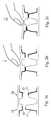
- FIG. 1 aschematically illustrates a sensor assembly in one embodiment of the invention.
- the sensor assemblyincludes a first layer 40 defining a front side surface 41 , which is a coordinate input surface.
- the sensor assemblyincludes a second layer 46 , separated from the first layer 40 by a gap. Pillars may however be formed between the two layers 40 , 46 at some locations (not illustrated).
- the gapmay be filled with liquid crystal, as used in liquid crystal displays, or with another fluid.
- Two spacersherein referred to as left upper spacer 42 and right upper spacer 43 , are formed on the first layer 40 extending from the surface of the first layer 40 opposite to the front side surface 41 .
- a conductive elementherein referred to as left second conductive element 12 , is formed on the bottom surface of the left upper spacer 42 .
- Another conductive elementherein referred to as right second conductive element 22 , is formed on the bottom surface of the right upper spacer 43 .
- a cover sheet of plastic or glassmay form the upper part of the first layer 40 . The cover sheet of plastic or glass may act as a protecting element.
- the second layer 46defines two spacers, herein referred to as left lower spacer 44 and right lower spacer 45 , extending towards the first layer 40 .
- Two conductive elementsherein referred to as left first conductive element 11 and left third conductive element 13 , are formed on the left lower spacer 44 in such a manner that a gap is formed between the left first conductive element 11 and the left third conductive element 13 on the top surface of the left lower spacer 44 .
- Two conductive elements, herein referred to as right first conductive element 21 and right third conductive element 23are formed on the right lower spacer 45 in such a manner that a gap is formed between the right first conductive element 21 and the right third conductive element 23 on the top surface of the right lower spacer 45 .
- FIG. 1 a(as well as on FIGS. 1 b - 7 d ) schematically represent signal lines leading to a control unit (not illustrated).
- the signal linesmay be formed along the direction of the cross-section illustrated in FIG. 1 a or may be formed in any other directions.
- Contact holes through insulating layersmay also be formed to lead the signal lines to the control unit (see for instance exemplary contact hole 71 on FIG. 3 of US 2008/0018613 A1).
- the left upper spacer 42 , the left second conductive element 12 , the left lower spacer 44 , the left first conductive element 11 and the left third conductive element 13form the first switching assembly 10 .
- the right upper spacer 43 , the right second conductive element 22 , the right lower spacer 45 , the right first conductive element 21 and the right third conductive element 23form the second switching assembly 20 .
- the first switching assembly 10 and the second switching assembly 20form a force measuring assembly, which is driven by a control unit or driving unit (not illustrated), configured for determining how many contacts are formed. In the state illustrated in FIG. 1 a where no pressure is exerted on the front side surface 41 , no contact is formed.
- the first layer 40may be formed of a resilient material.
- the sensor assemblymay be used repetitively, wherein the same shape or substantially the same shape is recovered between each interaction.
- the distance between the bottom surface of the left upper spacer 42 , wherein the left second conductive element 12 is formed, and the top surface of the left lower spacer 44 , wherein the gap between the left first conductive element 11 and the left third conductive element 13 is formed,is smaller than the distance between the bottom surface of the right upper spacer 43 , wherein the right second conductive element 22 is formed, and the top surface of the right lower spacer 45 , wherein the gap between the right first conductive element 21 and the right third conductive element 23 is formed.
- thisis because the distance between the front side surface 41 and the bottom surface of the left upper spacer 42 is larger than the distance between the front side surface 41 and the bottom surface of the right upper spacer 43 .
- the distance between spacers 42 and 44 and the distance between spacers 43 and 45are equal, but a pillar made of soft material is formed in the vicinity of spacers 43 , 45 .
- a gradual force applied on the front side surface 41causes first the spacers 42 , 44 to contact each other and then later the spacers 43 , 45 to contact each other.
- More than one pillarmay provide the same function.
- Such a pillarmay also be called pillar spacer.
- FIG. 1 bwhere a finger is illustrated exerting a pressure on the front side surface 41 .
- the size of the depicted fingershould by no means be construed as implying any specific dimension of the layers and switch assemblies depicted under the finger.
- the depicted fingeris only illustrative of the force exerted on the front side surface 41 , wherein the force may be exerted not only by a finger, but also by a hand, a stylus or another object.
- the thickness of the two layers 40 , 46 , the heights of the spacers 42 , 43 , 44 , 45 and the size of the gap between the spacersmay be degrees of magnitude smaller than the size of a human finger. This also applies to FIGS.
- the distance between the front side surface 41 and the bottom of the second layer 46is smaller than 0.1 mm.
- the right upper spacer 43is caused to move downwards but does not come in contact with the right lower spacer 45 , because the gap between the right upper spacer 43 and the right lower spacer 45 is larger than the gap between the left upper spacer 42 and the left lower spacer 44 . No electric contact is formed at that stage between the right first conductive element 21 and the right third conductive element 23 . This absence of electric path can be detected.
- the spacersmay be made of soft material (such as for instance silicone rubber), so that the pressure exerted on the first layer 40 when the left upper spacer 42 and the left lower spacer 44 are already in contact with each other can be absorbed by a deformation of the spacers 42 , 44 .
- soft materialsuch as for instance silicone rubber
- the right upper spacer 43 and the right lower spacer 45can continue to be brought close to each other until their contact. Different softness characteristics for different spacers are possible. The softness, in combination with the respective dimensions of the spacers, may then determine the force required to activate each new level.
- the conductive elements 11 , 12 , 13 , 21 , 22 , 23are made of indium tin oxide (ITO) or of another transparent conductive material.
- the voltage (i.e., electric potential difference) applied to two conductive elementsmay for instance have a value around 1 or 2 V (Volts), and the current flowing when a contact is formed between two conductive elements may for instance be around the 10 ⁇ A (10 microampere).
- the embodiments of the inventionare however based on a touch sensing solution using micro-switch assemblies, not on a resistive touch sensing solution (although some embodiments of the invention may be combined therewith).
- a signal output (not illustrated) of the control unit representing the number of formed contactsmay be converted to a signal representing an estimated force.
- different actionsmay be triggered in the control logic of a user interface. For instance, if the measured force exceeds the first threshold force, a first action is carried out. If the measured force exceeds the second threshold force, a second action is carried out.
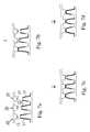
- FIGS. 2 a to 2 cschematically illustrate a cross-section of a sensor assembly at three stages of its operation, in one embodiment of the invention.
- the sensor assembly illustrated in FIG. 2 adiffers from the sensor assembly illustrated in FIG. 1 a in that, in FIG. 2 a , the left second conductive element 12 is connected to a signal line (symbolically illustrated by the dotted line in the upper left region of FIG. 2 a ), and the right second conductive element 22 is also connected to a signal line (symbolically illustrated by the dotted line in the upper right region of FIG. 2 a ).
- the signal lineslead to a control unit (not illustrated).
- the left second conductive element 12When a pressure is applied on the front side surface 41 , as illustrated in FIG. 2 b , the left second conductive element 12 is caused to move downwards and to contact the left first conductive element 11 . This contact may be detected, since an electric current can flow, in that state, between the left second conductive element 12 and the left first conductive element 11 .
- FIGS. 3 a to 3 cschematically illustrate a cross-section of a sensor assembly in another embodiment of the invention.
- the left second conductive element 12 and the right second conductive element 22form a single conductive element connected to a signal line (symbolically illustrated by the dotted line in the upper left region of FIG. 3 a ).
- a signal linesymbolically illustrated by the dotted line in the upper left region of FIG. 3 a .
- FIGS. 4 a to 4 cschematically illustrate a sensor assembly in another embodiment of the invention. It works as follows. If an electric contact is made between the left first conductive element 11 and the left third conductive element 13 through the left second conductive element 12 , this means that the force exerted on the front side surface 41 is larger than the first threshold force. If an electric contact is formed between the left first conductive element 11 and the right first conductive element 21 through the right second conductive element 22 and the left second conductive element 12 (which are permanently connected to each other), this means that the force exerted on the front side surface 41 is larger than the second threshold. In this embodiment, there are therefore also fewer signal lines to be arranged for detection purposes.
- FIGS. 5 a to 5 cschematically illustrate a sensor assembly in another embodiment of the invention.
- the left first conductive element 11 and the right first conductive element 21are permanently connected to each other. If an electric contact is made between the left first conductive element 11 and the left second conductive element 12 , this means that the force exerted on the front side surface 41 is larger than the first threshold. If an electric contact is made between the right first conductive element 21 (permanently connected to the left first conductive element 11 ) and the right second conductive element 22 , this means that the force exerted on the front side surface 41 is larger than the second threshold.
- FIGS. 6 a to 6 cschematically illustrate a variant of the sensor assembly illustrated in FIGS. 5 a to 5 c .
- the left lower spacer 44 and the right lower spacer 45form a single spacer having a profile such that the single lower spacer on the side of the left upper spacer 42 is higher than on the side of the right upper spacer 43 .
- FIGS. 1 a to 6 cother embodiments are contemplated by notably varying the position of the conductive elements and the shape of the spacers. These embodiments are within the scope of the invention.
- the number of contacts that can be made and which each correspond to a particular force thresholdmay be more than two. This is schematically illustrated in FIGS. 7 a to 7 d showing three pairs of spacers forming three switching assemblies 10 , 20 , 30 .
- FIG. 7 aWhen the force exerted on the front side surface 41 is smaller than a first threshold, no contact is made ( FIG. 7 a ).
- the applied forceis comprised between the first threshold force and a second threshold force, one contact is made ( FIG. 7 b , contact between conductive elements 11 and 12 ).
- FIG. 7 cWhen the applied force is larger than the second threshold force but smaller than a third threshold force, two contacts are made ( FIG. 7 c , contacts between conductive elements 11 and 12 and between conductive elements 21 and 22 ).
- FIG. 7 dcontacts between conductive elements 11 and 12 , between conductive elements 21 and 22 , and between conductive elements 31 and 32 ).
- FIG. 8schematically illustrates a sensor assembly wherein several force measurements can be made in different portions of a display or more generally coordinate input surface, in one embodiment of the invention.
- Switch assembliesmay be arranged in a distributed manner under substantially all regions of the coordinate input surface.
- the coordinate input surfacemay be the surface of a display or a touchpad for instance (this applies to all embodiments).
- FIG. 9schematically illustrates how signal lines for a sensor assembly may be implemented, in one embodiment of the invention.
- Signal lines X 1 a , X 1 b , X 1 c , and X 2 a , X 2 b , X 2 cmay be located on the bottom layer (second layer 46 ), while the signal lines Y 1 , Y 2 , Y 3 , Y 4 may be located on the upper layer (first layer 40 ).
- the signal linesare made, in one embodiment, of indium tin oxide (ITO).
- ITOindium tin oxide
- the sensor assemblymay further comprise, in addition to the force measuring units made of switch assemblies, capacitance measuring units (not illustrated) for measuring a capacitance between the first layer 40 and its surrounding environment.
- the surrounding environmentmay include a finger, hand or other object, which may modify the capacitance measured by the capacitance measuring unit, when active.
- the sensor assemblyis such that a capacitance measuring unit is configured to detect the presence of a finger, hand, stylus or other object on the front side surface 41 or in the vicinity thereof; and the at least one force measuring unit is configured to detect whether a force is exerted by the finger, hand, stylus or other object on the front side surface 41 .
- detecting whether a force is exerted by the finger, hand, stylus or other object on the front side surface 41means detecting that a force larger than first threshold value is exerted by the finger, hand, stylus or other object on the front side surface 41 .
- the at least one capacitance measuring unitis configured to detect the presence of a finger, hand or other object on the front side surface 41 or in the vicinity thereof; and the force measuring unit, including the first and second assemblies 10 , 20 , is configured to estimate the force exerted by the finger, hand, stylus or other object on the front side surface 41 . Therefore, yet more parameters may be used to control a device through a user interface. Namely the value of the force exerted by the finger, hand, stylus or other object on the front side surface 41 of the sensor assembly may also be used as an input parameter of the user interface.
- the force measuring unitincluding at least the first and second assemblies 10 , 20 and the control unit, is activated only when the capacitance measuring unit indicates a change of capacitance exceeding a threshold value. This saves power by not permanently activating the force measuring unit.
- the force measurement unitdoes not need to start until a signal from the capacitance measurement unit has indicated the presence of a user's finger, hand, stylus or other object.
- the sensor assemblyis, in one embodiment, transparent.
- the presence of a finger, hand, stylus or other object on the front side surface 41can be detected; the position of the finger, hand, stylus or other object on the front side surface 41 can be estimated; and the force exerted by the finger, hand, stylus or other object on the front side surface 41 can be also estimated.
- the inventionalso relates to a method of using a sensor assembly as described above, the method including steps of outputting a signal indicating the presence of a finger, hand, stylus or other object on the front side surface 41 or in the vicinity thereof; and outputting a signal indicating whether a force is exerted by the finger, hand, stylus or other object on the front side surface 41 .
- the inventionalso relates to a method of using a sensor assembly as described above, the method including steps of outputting a signal indicating the presence of a finger, hand, stylus or other object on the front side surface 41 or in the vicinity thereof; outputting a signal indicating the force is exerted by the finger, hand, stylus or other object on the front side surface 41 ; and outputting a signal indicating an estimation of the two-dimensional position of the finger, hand, stylus or other object on the front side surface 41 .
- the methodfurther includes outputting a signal indicating an estimation of the three-dimensional position of the finger, hand, stylus or other object on the front side surface 41 , based on the signal indicating an estimation of the two-dimensional position of the finger, hand, stylus or other object on the front side surface 41 , which provides coordinates x and y; and the signal indicating an estimation of the force exerted by the finger, hand, stylus or other object on the front side surface 41 , which provides coordinate z; wherein coordinates x and y correspond to two distinct directions along the front side surface 41 and coordinate z corresponds a direction perpendicular to the front side surface 41 .
- the physical entities according to the invention and/or its embodiments, including the controlling unit, the force measuring unit and the capacitance measuring unit,may comprise or store computer programs including instructions such that, when the computer programs are executed on the physical entities, steps, procedures and functions of these units are carried out according to embodiments of the invention.
- the inventionalso relates to such computer programs for carrying out the function of the units, and to any computer-readable medium storing the computer programs for carrying out methods according to the invention.
- control unitforce measuring unit
- capacitor measuring unitcapacitive measuring unit
- Any one of the above-referred unitsmay be implemented in hardware, software, field-programmable gate array (FPGA), application-specific integrated circuit (ASICs), firmware or the like.
- FPGAfield-programmable gate array
- ASICsapplication-specific integrated circuit
- control unit, the force measuring unit and the capacitance measuring unitare respectively replaced by controlling means, force measuring means and capacitance measuring means, or by a controller, a force measurer and a capacitance measurer, for performing the functions of the control unit, force measuring unit and capacitance measuring unit respectively.
- any one of the above-described stepsmay be implemented using computer-readable instructions, for instance in the form of computer-understandable procedures, methods or the like, in any kind of computer languages, and/or in the form of embedded software on firmware, integrated circuits or the like.
Landscapes
- Engineering & Computer Science (AREA)
- General Engineering & Computer Science (AREA)
- Theoretical Computer Science (AREA)
- Human Computer Interaction (AREA)
- Physics & Mathematics (AREA)
- General Physics & Mathematics (AREA)
- Position Input By Displaying (AREA)
- Force Measurement Appropriate To Specific Purposes (AREA)
- User Interface Of Digital Computer (AREA)
Abstract
Description
- (i) when no force is exerted on the region of the coordinate input surface or when a force smaller than a first threshold force is exerted thereon, the first and second conductive elements of the first switch assembly are not in contact with each other and the first and second conductive elements of the second switch assembly are not in contact with each other;
- (ii) when a force larger than the first threshold force and smaller than a second threshold force is exerted on the region of the coordinate input surface, the first and second conductive elements of the first switch assembly are in contact with each other and the first and second conductive elements of the second switch assembly are not in contact with each other; and
- (iii) when a force larger than the second threshold force is exerted on the region of the coordinate input surface, the first and second conductive elements of the first switch assembly are in contact with each other and the first and second conductive elements of the second switch assembly are also in contact with each other.
Claims (8)
Priority Applications (3)
| Application Number | Priority Date | Filing Date | Title |
|---|---|---|---|
| US12/503,293US8120588B2 (en) | 2009-07-15 | 2009-07-15 | Sensor assembly and display including a sensor assembly |
| PCT/EP2010/050005WO2011006678A1 (en) | 2009-07-15 | 2010-01-04 | Sensor assembly and display including a sensor assembly |
| TW099115594ATW201106224A (en) | 2009-07-15 | 2010-05-14 | Sensor assembly and display including a sensor assembly |
Applications Claiming Priority (1)
| Application Number | Priority Date | Filing Date | Title |
|---|---|---|---|
| US12/503,293US8120588B2 (en) | 2009-07-15 | 2009-07-15 | Sensor assembly and display including a sensor assembly |
Publications (2)
| Publication Number | Publication Date |
|---|---|
| US20110011650A1 US20110011650A1 (en) | 2011-01-20 |
| US8120588B2true US8120588B2 (en) | 2012-02-21 |
Family
ID=42026813
Family Applications (1)
| Application Number | Title | Priority Date | Filing Date |
|---|---|---|---|
| US12/503,293Expired - Fee RelatedUS8120588B2 (en) | 2009-07-15 | 2009-07-15 | Sensor assembly and display including a sensor assembly |
Country Status (3)
| Country | Link |
|---|---|
| US (1) | US8120588B2 (en) |
| TW (1) | TW201106224A (en) |
| WO (1) | WO2011006678A1 (en) |
Cited By (22)
| Publication number | Priority date | Publication date | Assignee | Title |
|---|---|---|---|---|
| US20120199448A1 (en)* | 2011-02-09 | 2012-08-09 | Liebherr-Elektronik Gmbh | Short-travel key |
| US8587422B2 (en) | 2010-03-31 | 2013-11-19 | Tk Holdings, Inc. | Occupant sensing system |
| US8725230B2 (en) | 2010-04-02 | 2014-05-13 | Tk Holdings Inc. | Steering wheel with hand sensors |
| US9007190B2 (en) | 2010-03-31 | 2015-04-14 | Tk Holdings Inc. | Steering wheel sensors |
| US9032818B2 (en) | 2012-07-05 | 2015-05-19 | Nextinput, Inc. | Microelectromechanical load sensor and methods of manufacturing the same |
| US9487388B2 (en) | 2012-06-21 | 2016-11-08 | Nextinput, Inc. | Ruggedized MEMS force die |
| US9696223B2 (en) | 2012-09-17 | 2017-07-04 | Tk Holdings Inc. | Single layer force sensor |
| US9727031B2 (en) | 2012-04-13 | 2017-08-08 | Tk Holdings Inc. | Pressure sensor including a pressure sensitive material for use with control systems and methods of using the same |
| US9902611B2 (en) | 2014-01-13 | 2018-02-27 | Nextinput, Inc. | Miniaturized and ruggedized wafer level MEMs force sensors |
| US10466119B2 (en) | 2015-06-10 | 2019-11-05 | Nextinput, Inc. | Ruggedized wafer level MEMS force sensor with a tolerance trench |
| US10545389B2 (en) | 2016-12-05 | 2020-01-28 | E Ink Holdings Inc. | Electrophoretic display panel |
| US10962427B2 (en) | 2019-01-10 | 2021-03-30 | Nextinput, Inc. | Slotted MEMS force sensor |
| US11221263B2 (en) | 2017-07-19 | 2022-01-11 | Nextinput, Inc. | Microelectromechanical force sensor having a strain transfer layer arranged on the sensor die |
| US11243126B2 (en) | 2017-07-27 | 2022-02-08 | Nextinput, Inc. | Wafer bonded piezoresistive and piezoelectric force sensor and related methods of manufacture |
| US11243125B2 (en) | 2017-02-09 | 2022-02-08 | Nextinput, Inc. | Integrated piezoresistive and piezoelectric fusion force sensor |
| US11255737B2 (en) | 2017-02-09 | 2022-02-22 | Nextinput, Inc. | Integrated digital force sensors and related methods of manufacture |
| US11275475B2 (en) | 2019-04-30 | 2022-03-15 | Apple Inc. | Compliant material for protecting capacitive force sensors and increasing capacitive sensitivity |
| US11385108B2 (en) | 2017-11-02 | 2022-07-12 | Nextinput, Inc. | Sealed force sensor with etch stop layer |
| US11423686B2 (en) | 2017-07-25 | 2022-08-23 | Qorvo Us, Inc. | Integrated fingerprint and force sensor |
| US11579028B2 (en) | 2017-10-17 | 2023-02-14 | Nextinput, Inc. | Temperature coefficient of offset compensation for force sensor and strain gauge |
| US11592946B1 (en) | 2021-09-21 | 2023-02-28 | Apple Inc. | Capacitive gap force sensor with multi-layer fill |
| US11874185B2 (en) | 2017-11-16 | 2024-01-16 | Nextinput, Inc. | Force attenuator for force sensor |
Families Citing this family (45)
| Publication number | Priority date | Publication date | Assignee | Title |
|---|---|---|---|---|
| US8947383B2 (en) | 2008-01-04 | 2015-02-03 | Tactus Technology, Inc. | User interface system and method |
| US20160187981A1 (en) | 2008-01-04 | 2016-06-30 | Tactus Technology, Inc. | Manual fluid actuator |
| US9588683B2 (en) | 2008-01-04 | 2017-03-07 | Tactus Technology, Inc. | Dynamic tactile interface |
| US8704790B2 (en) | 2010-10-20 | 2014-04-22 | Tactus Technology, Inc. | User interface system |
| US9052790B2 (en) | 2008-01-04 | 2015-06-09 | Tactus Technology, Inc. | User interface and methods |
| US9552065B2 (en) | 2008-01-04 | 2017-01-24 | Tactus Technology, Inc. | Dynamic tactile interface |
| US9612659B2 (en) | 2008-01-04 | 2017-04-04 | Tactus Technology, Inc. | User interface system |
| US8922510B2 (en) | 2008-01-04 | 2014-12-30 | Tactus Technology, Inc. | User interface system |
| US9298261B2 (en) | 2008-01-04 | 2016-03-29 | Tactus Technology, Inc. | Method for actuating a tactile interface layer |
| US8243038B2 (en) | 2009-07-03 | 2012-08-14 | Tactus Technologies | Method for adjusting the user interface of a device |
| US8456438B2 (en) | 2008-01-04 | 2013-06-04 | Tactus Technology, Inc. | User interface system |
| US9274612B2 (en) | 2008-01-04 | 2016-03-01 | Tactus Technology, Inc. | User interface system |
| US9423875B2 (en) | 2008-01-04 | 2016-08-23 | Tactus Technology, Inc. | Dynamic tactile interface with exhibiting optical dispersion characteristics |
| US9128525B2 (en) | 2008-01-04 | 2015-09-08 | Tactus Technology, Inc. | Dynamic tactile interface |
| US8547339B2 (en) | 2008-01-04 | 2013-10-01 | Tactus Technology, Inc. | System and methods for raised touch screens |
| US8154527B2 (en) | 2008-01-04 | 2012-04-10 | Tactus Technology | User interface system |
| US9557915B2 (en) | 2008-01-04 | 2017-01-31 | Tactus Technology, Inc. | Dynamic tactile interface |
| US9720501B2 (en) | 2008-01-04 | 2017-08-01 | Tactus Technology, Inc. | Dynamic tactile interface |
| US9063627B2 (en) | 2008-01-04 | 2015-06-23 | Tactus Technology, Inc. | User interface and methods |
| US9430074B2 (en) | 2008-01-04 | 2016-08-30 | Tactus Technology, Inc. | Dynamic tactile interface |
| US9588684B2 (en) | 2009-01-05 | 2017-03-07 | Tactus Technology, Inc. | Tactile interface for a computing device |
| WO2011003113A1 (en) | 2009-07-03 | 2011-01-06 | Tactus Technology | User interface enhancement system |
| WO2011087816A1 (en)* | 2009-12-21 | 2011-07-21 | Tactus Technology | User interface system |
| CN102782617B (en) | 2009-12-21 | 2015-10-07 | 泰克图斯科技公司 | User interface system |
| US9298262B2 (en) | 2010-01-05 | 2016-03-29 | Tactus Technology, Inc. | Dynamic tactile interface |
| WO2011112984A1 (en) | 2010-03-11 | 2011-09-15 | Tactus Technology | User interface system |
| WO2011133605A1 (en) | 2010-04-19 | 2011-10-27 | Tactus Technology | Method of actuating a tactile interface layer |
| WO2011133604A1 (en) | 2010-04-19 | 2011-10-27 | Tactus Technology | User interface system |
| CN103124946B (en) | 2010-10-20 | 2016-06-29 | 泰克图斯科技公司 | User interface system and method |
| US9372588B2 (en) | 2011-05-19 | 2016-06-21 | Microsoft Technology Licensing, Llc | Pressure-sensitive multi-touch device |
| CN102819330B (en)* | 2011-06-07 | 2016-07-06 | 索尼爱立信移动通讯有限公司 | Electronic equipment, pressure detection method and pressure-detecting device |
| JP5838056B2 (en)* | 2011-08-11 | 2015-12-24 | 富士通コンポーネント株式会社 | Switches and connectors |
| US9460029B2 (en) | 2012-03-02 | 2016-10-04 | Microsoft Technology Licensing, Llc | Pressure sensitive keys |
| US9405417B2 (en) | 2012-09-24 | 2016-08-02 | Tactus Technology, Inc. | Dynamic tactile interface and methods |
| WO2014047656A2 (en) | 2012-09-24 | 2014-03-27 | Tactus Technology, Inc. | Dynamic tactile interface and methods |
| US9557813B2 (en) | 2013-06-28 | 2017-01-31 | Tactus Technology, Inc. | Method for reducing perceived optical distortion |
| JP2015088332A (en)* | 2013-10-30 | 2015-05-07 | パナソニックIpマネジメント株式会社 | Pressure-sensitive switch and manufacturing method thereof, touch panel including pressure-sensitive switch and manufacturing method thereof |
| JP2015197300A (en)* | 2014-03-31 | 2015-11-09 | パナソニックIpマネジメント株式会社 | PRESSURE-SENSITIVE ELEMENT AND MANUFACTURING METHOD THEREOF, TOUCH PANEL EQUIPPED WITH PRESSURE-SENSITIVE ELEMENT AND ITS MANUFACTURING METHOD |
| JP2015197299A (en)* | 2014-03-31 | 2015-11-09 | パナソニックIpマネジメント株式会社 | Pressure sensitive element, manufacturing method thereof, touch panel including pressure sensitive element and manufacturing method thereof |
| JP6325639B1 (en)* | 2016-11-22 | 2018-05-16 | Nissha株式会社 | Pressure sensor |
| DE102018126472A1 (en)* | 2018-10-24 | 2020-04-30 | Valeo Schalter Und Sensoren Gmbh | Input device for a motor vehicle and method for controlling the input device |
| DE102020108704A1 (en) | 2020-03-30 | 2021-09-30 | Valeo Schalter Und Sensoren Gmbh | Sensor device for an operator input device |
| US11726597B1 (en)* | 2022-05-27 | 2023-08-15 | Microsoft Technology Licensing, Llc | Differential capacitive force sensing |
| US20240011850A1 (en)* | 2022-07-06 | 2024-01-11 | Electronics And Telecommunications Research Institute | Flexible pressure sensor |
| US12099667B1 (en) | 2023-05-19 | 2024-09-24 | Microsoft Technology Licensing, Llc | Force sensing touchpad |
Citations (11)
| Publication number | Priority date | Publication date | Assignee | Title |
|---|---|---|---|---|
| US20010043189A1 (en) | 1998-06-12 | 2001-11-22 | Michel A. Brisebois | Active edge user interface |
| EP1351121A2 (en) | 2002-03-26 | 2003-10-08 | Polymatech Co., Ltd. | Input Device |
| US6857800B2 (en)* | 2001-04-24 | 2005-02-22 | Inventec Appliances Corp. | Method for inputting different characters by multi-directionally pressing a single key more than one time |
| US20050052425A1 (en)* | 2003-08-18 | 2005-03-10 | Zadesky Stephen Paul | Movable touch pad with added functionality |
| US6943705B1 (en)* | 2002-05-03 | 2005-09-13 | Synaptics, Inc. | Method and apparatus for providing an integrated membrane switch and capacitive sensor |
| US7064561B2 (en)* | 2002-07-05 | 2006-06-20 | Nitta Corporation | Resistance type sensor |
| EP1816662A2 (en) | 2006-02-06 | 2007-08-08 | LG Electronics Inc. | Mobile terminal key input device and method |
| US7255011B2 (en)* | 2005-05-31 | 2007-08-14 | Nitta Corporation | Resistance type sensor |
| US20080018613A1 (en) | 2006-07-18 | 2008-01-24 | Dong-Gyu Kim | Touch screen display apparatus and method of driving the same |
| US20090140996A1 (en)* | 2007-11-29 | 2009-06-04 | Sony Corporation | Press detection sensor, input device and electronic apparatus |
| US7825911B2 (en)* | 2006-03-27 | 2010-11-02 | Sanyo Electric Co., Ltd. | Touch sensor, touch pad and input device |
- 2009
- 2009-07-15USUS12/503,293patent/US8120588B2/ennot_activeExpired - Fee Related
- 2010
- 2010-01-04WOPCT/EP2010/050005patent/WO2011006678A1/enactiveApplication Filing
- 2010-05-14TWTW099115594Apatent/TW201106224A/enunknown
Patent Citations (12)
| Publication number | Priority date | Publication date | Assignee | Title |
|---|---|---|---|---|
| US20010043189A1 (en) | 1998-06-12 | 2001-11-22 | Michel A. Brisebois | Active edge user interface |
| US6369803B2 (en)* | 1998-06-12 | 2002-04-09 | Nortel Networks Limited | Active edge user interface |
| US6857800B2 (en)* | 2001-04-24 | 2005-02-22 | Inventec Appliances Corp. | Method for inputting different characters by multi-directionally pressing a single key more than one time |
| EP1351121A2 (en) | 2002-03-26 | 2003-10-08 | Polymatech Co., Ltd. | Input Device |
| US6943705B1 (en)* | 2002-05-03 | 2005-09-13 | Synaptics, Inc. | Method and apparatus for providing an integrated membrane switch and capacitive sensor |
| US7064561B2 (en)* | 2002-07-05 | 2006-06-20 | Nitta Corporation | Resistance type sensor |
| US20050052425A1 (en)* | 2003-08-18 | 2005-03-10 | Zadesky Stephen Paul | Movable touch pad with added functionality |
| US7255011B2 (en)* | 2005-05-31 | 2007-08-14 | Nitta Corporation | Resistance type sensor |
| EP1816662A2 (en) | 2006-02-06 | 2007-08-08 | LG Electronics Inc. | Mobile terminal key input device and method |
| US7825911B2 (en)* | 2006-03-27 | 2010-11-02 | Sanyo Electric Co., Ltd. | Touch sensor, touch pad and input device |
| US20080018613A1 (en) | 2006-07-18 | 2008-01-24 | Dong-Gyu Kim | Touch screen display apparatus and method of driving the same |
| US20090140996A1 (en)* | 2007-11-29 | 2009-06-04 | Sony Corporation | Press detection sensor, input device and electronic apparatus |
Non-Patent Citations (4)
| Title |
|---|
| 2008 Tech Forum, Evolution of Technology & Creating New Businesses-Samsung LCD Business-, Dec. 8, 2008, Jun H. Souk, Executive VP Samsung Electronics; http://www.samsung.com/sec/aboutsamsung/file/ir/irevent/analystday/2008/tech-forum-2008-004.pdf. |
| Bonnie C. Baker, Wendy Fang, "Powering resistive touch screens efficiently", Planet Analog, May 28, 2007 (3:16 PM), URL:http://www.planetanalog.com/showArticle?articleID=199702778. |
| International Search Report, corresponding to PCT/EP2010/050005, mailed on Mar. 31, 2010. |
| Written Opinion, corresponding to PCT/EP2010/050005, mailed on Mar. 31, 2010. |
Cited By (34)
| Publication number | Priority date | Publication date | Assignee | Title |
|---|---|---|---|---|
| US8587422B2 (en) | 2010-03-31 | 2013-11-19 | Tk Holdings, Inc. | Occupant sensing system |
| US9007190B2 (en) | 2010-03-31 | 2015-04-14 | Tk Holdings Inc. | Steering wheel sensors |
| US8725230B2 (en) | 2010-04-02 | 2014-05-13 | Tk Holdings Inc. | Steering wheel with hand sensors |
| US20120199448A1 (en)* | 2011-02-09 | 2012-08-09 | Liebherr-Elektronik Gmbh | Short-travel key |
| US9727031B2 (en) | 2012-04-13 | 2017-08-08 | Tk Holdings Inc. | Pressure sensor including a pressure sensitive material for use with control systems and methods of using the same |
| US9487388B2 (en) | 2012-06-21 | 2016-11-08 | Nextinput, Inc. | Ruggedized MEMS force die |
| US9493342B2 (en) | 2012-06-21 | 2016-11-15 | Nextinput, Inc. | Wafer level MEMS force dies |
| US9032818B2 (en) | 2012-07-05 | 2015-05-19 | Nextinput, Inc. | Microelectromechanical load sensor and methods of manufacturing the same |
| US9696223B2 (en) | 2012-09-17 | 2017-07-04 | Tk Holdings Inc. | Single layer force sensor |
| US9902611B2 (en) | 2014-01-13 | 2018-02-27 | Nextinput, Inc. | Miniaturized and ruggedized wafer level MEMs force sensors |
| US10466119B2 (en) | 2015-06-10 | 2019-11-05 | Nextinput, Inc. | Ruggedized wafer level MEMS force sensor with a tolerance trench |
| US10545389B2 (en) | 2016-12-05 | 2020-01-28 | E Ink Holdings Inc. | Electrophoretic display panel |
| US11255737B2 (en) | 2017-02-09 | 2022-02-22 | Nextinput, Inc. | Integrated digital force sensors and related methods of manufacture |
| US11946817B2 (en) | 2017-02-09 | 2024-04-02 | DecaWave, Ltd. | Integrated digital force sensors and related methods of manufacture |
| US11243125B2 (en) | 2017-02-09 | 2022-02-08 | Nextinput, Inc. | Integrated piezoresistive and piezoelectric fusion force sensor |
| US11808644B2 (en) | 2017-02-09 | 2023-11-07 | Qorvo Us, Inc. | Integrated piezoresistive and piezoelectric fusion force sensor |
| US11604104B2 (en) | 2017-02-09 | 2023-03-14 | Qorvo Us, Inc. | Integrated piezoresistive and piezoelectric fusion force sensor |
| US11221263B2 (en) | 2017-07-19 | 2022-01-11 | Nextinput, Inc. | Microelectromechanical force sensor having a strain transfer layer arranged on the sensor die |
| US11423686B2 (en) | 2017-07-25 | 2022-08-23 | Qorvo Us, Inc. | Integrated fingerprint and force sensor |
| US11609131B2 (en) | 2017-07-27 | 2023-03-21 | Qorvo Us, Inc. | Wafer bonded piezoresistive and piezoelectric force sensor and related methods of manufacture |
| US11243126B2 (en) | 2017-07-27 | 2022-02-08 | Nextinput, Inc. | Wafer bonded piezoresistive and piezoelectric force sensor and related methods of manufacture |
| US11946816B2 (en) | 2017-07-27 | 2024-04-02 | Nextinput, Inc. | Wafer bonded piezoresistive and piezoelectric force sensor and related methods of manufacture |
| US12203819B2 (en) | 2017-10-17 | 2025-01-21 | Nextinput, Inc. | Temperature coefficient of offset compensation for force sensor and strain gauge |
| US11579028B2 (en) | 2017-10-17 | 2023-02-14 | Nextinput, Inc. | Temperature coefficient of offset compensation for force sensor and strain gauge |
| US11898918B2 (en) | 2017-10-17 | 2024-02-13 | Nextinput, Inc. | Temperature coefficient of offset compensation for force sensor and strain gauge |
| US12332127B2 (en) | 2017-11-02 | 2025-06-17 | Nextinput, Inc. | Sealed force sensor with etch stop layer |
| US11385108B2 (en) | 2017-11-02 | 2022-07-12 | Nextinput, Inc. | Sealed force sensor with etch stop layer |
| US11965787B2 (en) | 2017-11-02 | 2024-04-23 | Nextinput, Inc. | Sealed force sensor with etch stop layer |
| US11874185B2 (en) | 2017-11-16 | 2024-01-16 | Nextinput, Inc. | Force attenuator for force sensor |
| US10962427B2 (en) | 2019-01-10 | 2021-03-30 | Nextinput, Inc. | Slotted MEMS force sensor |
| US11698310B2 (en) | 2019-01-10 | 2023-07-11 | Nextinput, Inc. | Slotted MEMS force sensor |
| US12416534B2 (en) | 2019-01-10 | 2025-09-16 | Nextinput, Inc. | Slotted MEMS force sensor |
| US11275475B2 (en) | 2019-04-30 | 2022-03-15 | Apple Inc. | Compliant material for protecting capacitive force sensors and increasing capacitive sensitivity |
| US11592946B1 (en) | 2021-09-21 | 2023-02-28 | Apple Inc. | Capacitive gap force sensor with multi-layer fill |
Also Published As
| Publication number | Publication date |
|---|---|
| TW201106224A (en) | 2011-02-16 |
| US20110011650A1 (en) | 2011-01-20 |
| WO2011006678A1 (en) | 2011-01-20 |
Similar Documents
| Publication | Publication Date | Title |
|---|---|---|
| US8120588B2 (en) | Sensor assembly and display including a sensor assembly | |
| EP2526471B1 (en) | Touch sensing device, touch screen device comprising the touch sensing device, mobile device, method for sensing a touch and method for manufacturing a touch sensing device | |
| CN205302226U (en) | Electronic equipment with force transducer | |
| KR102425824B1 (en) | Haptic driving method and apparatus in flexible display | |
| RU2454702C1 (en) | One-sided capacitive force sensor for electronic devices | |
| JP6485618B2 (en) | Piezoelectric sheet, touch panel using the same, and input / output device using them | |
| KR102636735B1 (en) | Display Device | |
| EP2041641B1 (en) | Input device | |
| KR101452660B1 (en) | Touch screen rendering system and method of operation thereof | |
| TWI621986B (en) | Pressure sensing touch display device | |
| CN105117058B (en) | A kind of touch panel, touch-control display panel and electronic equipment | |
| KR101301277B1 (en) | Input device with membrane pressure sensor and proximity sensor. | |
| JP7232178B2 (en) | Touch input method and device for providing user interface | |
| KR101362843B1 (en) | Touch screen apparatus and method thereof | |
| JP2009122969A (en) | Screen input type image display device | |
| KR20110123093A (en) | Touch screen device | |
| JP6431610B2 (en) | Capacitive input device | |
| CN101738765A (en) | Liquid crystal display panel with integrated touch screen, device and touch detection method | |
| KR20100019810A (en) | Touch screen system | |
| KR20100074820A (en) | Touch screen panel and method of manufacturing the same | |
| US10671201B2 (en) | Touch substrate, touch display panel and display device | |
| KR20120052044A (en) | Input device with membrane pressure sensor and proximity sensor and a method using the same | |
| KR20170060525A (en) | Touch Pressure Sensor | |
| KR101927795B1 (en) | Touch input device for sensing a position and a pressure magnitude of touch | |
| KR20190038770A (en) | Force-touch panel, and fource-touch detection device and display system having the same |
Legal Events
| Date | Code | Title | Description |
|---|---|---|---|
| AS | Assignment | Owner name:SONY ERICSSON MOBILE COMMUNICATIONS AB, SWEDEN Free format text:ASSIGNMENT OF ASSIGNORS INTEREST;ASSIGNOR:KLINGHULT, GUNNAR;REEL/FRAME:022958/0153 Effective date:20090525 | |
| STCF | Information on status: patent grant | Free format text:PATENTED CASE | |
| FPAY | Fee payment | Year of fee payment:4 | |
| AS | Assignment | Owner name:SONY MOBILE COMMUNICATIONS AB, SWEDEN Free format text:CHANGE OF NAME;ASSIGNOR:SONY ERICSSON MOBILE COMMUNICATIONS AB;REEL/FRAME:048690/0974 Effective date:20120221 | |
| AS | Assignment | Owner name:SONY CORPORATION, JAPAN Free format text:ASSIGNMENT OF ASSIGNORS INTEREST;ASSIGNOR:SONY MOBILE COMMUNICATIONS AB;REEL/FRAME:048825/0737 Effective date:20190405 | |
| FEPP | Fee payment procedure | Free format text:MAINTENANCE FEE REMINDER MAILED (ORIGINAL EVENT CODE: REM.); ENTITY STATUS OF PATENT OWNER: LARGE ENTITY | |
| LAPS | Lapse for failure to pay maintenance fees | Free format text:PATENT EXPIRED FOR FAILURE TO PAY MAINTENANCE FEES (ORIGINAL EVENT CODE: EXP.); ENTITY STATUS OF PATENT OWNER: LARGE ENTITY | |
| STCH | Information on status: patent discontinuation | Free format text:PATENT EXPIRED DUE TO NONPAYMENT OF MAINTENANCE FEES UNDER 37 CFR 1.362 | |
| FP | Lapsed due to failure to pay maintenance fee | Effective date:20200221 |