US8120380B2 - Comprehensive application power tester - Google Patents
Comprehensive application power testerDownload PDFInfo
- Publication number
- US8120380B2 US8120380B2US09/823,079US82307901AUS8120380B2US 8120380 B2US8120380 B2US 8120380B2US 82307901 AUS82307901 AUS 82307901AUS 8120380 B2US8120380 B2US 8120380B2
- Authority
- US
- United States
- Prior art keywords
- voltage
- disturbance
- power supply
- controllable
- supply voltage
- Prior art date
- Legal status (The legal status is an assumption and is not a legal conclusion. Google has not performed a legal analysis and makes no representation as to the accuracy of the status listed.)
- Expired - Fee Related, expires
Links
Images


Classifications
- G—PHYSICS
- G01—MEASURING; TESTING
- G01R—MEASURING ELECTRIC VARIABLES; MEASURING MAGNETIC VARIABLES
- G01R31/00—Arrangements for testing electric properties; Arrangements for locating electric faults; Arrangements for electrical testing characterised by what is being tested not provided for elsewhere
- G01R31/40—Testing power supplies
Definitions
- the present inventionrelates generally to testing electronic devices and components. More particularly, the present invention relates to testing disc drives and other devices under stress conditions.
- Preventing damage from power disturbances in electronic devicesis vital to the success of a product. If damaged from a power disturbance, a highly sensitive electronic device may be impaired from working properly. Some of the problems caused by power disturbances may include hardware malfunctioning, integrated circuits being rendered ineffective, memory being rewritten or lost, software and firmware erased, or data may be lost. If an electronic device is damaged by a power disturbance, the product will probably have to be completely replaced. Thus, there clearly exists a need to test the design capabilities of an electronic device to discern if the device is capable of handling the power disruptions for which it may encounter.
- the present inventionprovides a solution to this and other problems, and offers other advantages over the prior art.
- the present inventionrelates to a power testing system which solves the above-mentioned problem.
- an electronic device power testing methodin which applying a nominal voltage to an electronic component, introducing a voltage disruption to the nominal voltage, and repeating the voltage disruption for a specified number of instances is done.
- the present inventionalso can be implemented as an electronic device power tester.
- FIG. 1is a block diagram in accordance with one preferred embodiment of the present invention.
- FIG. 2is a schematic of one preferred embodiment of a power control module that can be used in the system shown in FIG. 1 .
- FIG. 3is a schematic of a digital to analog converter and a multiplier which can be used with the power control module shown in FIG. 2 .
- FIG. 4is a schematic of one preferred embodiment of the power sequencing in accordance with one aspect of the present invention.
- FIG. 5illustrates timing diagrams of the power output signals in accordance with one embodiment of the present invention.
- the present inventionprovides a solution to the above identified problem.
- the present inventionhas multiple uses including testing the design of electronic devices by supplying various voltage disturbances, sequences, and interruptions to the electronic device.
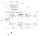
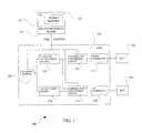
- FIG. 1is a block diagram of a comprehensive application power tester 100 in accordance with one preferred embodiment of the present invention.
- a systemlike the one shown in FIG. 1 includes a computer 101 , computer software 102 , a multifunction input/output (I/O) board 103 , a power control module (PCM) 104 , and at least one device under test (DUT) 105 .
- I/Oinput/output
- PCMpower control module
- DUTdevice under test
- the software program 102communicates with the PCM 104 through the I/O board 103 .
- the software systemprovides a graphical user interface (GUI) (not shown) in which the operator can input requirements while testing.
- GUIgraphical user interface
- the I/O board 103allows two-way communication between the computer 101 and the PCM 104 .
- the I/O board 103provides 3 counters/timers, 2 digital to analog (D/A) channels, 24 digital I/O lines, and 8 analog to digital (A/D) input channels.
- the PCM 104is connected to the I/O board 103 by a multiple conductor ribbon cable (not shown).
- the PCM 104includes an AC power switch 106 , a +5 Volt DC and a +12 Volt DC power source 107 , a +24 Volt DC power source 108 , a variable low disturbance switch 109 , a variable peak disturbance switch 110 , a down connector 111 , and an up connector 112 .
- a DUT 105is connected to the PCM 104 via a power connector (not shown).
- the DUT 105can be connected to the PCM 104 at either the down connector 111 or the up connector 112 .
- a second DUT 105may be connected to either the up connector 112 or the down connector 111 .
- FIG. 2illustrates a variable low disturbance switch 204 and a variable peak disturbance switch 205 as well as the other components of the PCM 104 , including the 120 Volt AC power supply 206 , the +5 Volt DC and +12 Volt DC power supply 207 , the +24 Volt DC power supply 208 , the up connector 212 , and the down connector 211 .
- the variable peak disturbance switch 110consists of bipolar NPN transistor 220 and transistor 222 .
- Transistor 220 and transistor 222are configured as emitter follower circuits to the DUT.
- the voltage source for transistor 220 and transistor 222is the +24 Volt DC power supply 208 .
- the emitter of transistor 220is a common node with the cathode of diode 224 and the emitter of transistor 220 is a common node with the cathode of diode 226 .
- poweris provided to the DUT via diodes 224 and 226 , respectively.
- poweris provided by transistors 220 and 222 in linear conduction mode, with the voltages determined by the voltage at each of the transistor's base.
- the base voltagesare set by operational amplifiers 230 and 232 , respectively.
- Operational amplifiers 230 and 232are configured as non-inverting amplifiers with positive terminal inputs set by two of the multifunction I/O board's digital-toanalog converters (DAC), 240 and 242 .
- Transistor 220 ′s and 222 ′s base networksinclude individual, high voltage, open collector drivers 260 and 262 , which are normally in a non-asserted state.
- Resistors 250 and 252dissipate the individual operational amplifiers 230 and 232 voltages while high voltage, open collector drivers 260 and 262 , are in a non-asserted state and transistors 220 and 222 are in a non-conduct state.
- Voltage disruption frequency and voltage disruption time durationare determined by counter timers on the multifunction I/O board, specifically, 255 .
- line 255asserts a voltage disruption
- each of the individual high voltage drivers, 260 and 262outputs assert to the operational amplifier's voltage, which is then reflected at the base terminals of transistors 220 and 222 .
- the resultis a controlled voltage spike for a specific duration.
- the variable low disturbance switchconsists of an analog switch 271 , a transistor 272 , an operational amplifier 311 , and a voltage divider consisting of resistors 273 and 274 .
- the voltageis controlled by the output of operational amplifier 311 and the voltage divider circuit, resistors 273 and 274 .
- the voltage provided to the voltage divider, resistors 273 and 274is determined by a DAC output, 312 , from the DAC integrated circuit 310 .
- the voltage output from the DAC output, 312is programmed using three digital I/O lines 320 , 321 , and 322 .
- FIG. 3shows the clock input 320 to the DAC 310 . Also shown are the chip select input 321 and the data input 322 . Lines 320 , 321 , and 322 provide the ability to program the individual DAC outputs of the DAC integrated circuit 310 with a serial data stream.
- a variable low voltage disturbanceoccurs when the analog switch, 271 , between the gate of transistor 270 and the output of operational amplifier 232 is closed(on). During that time transistor 270 ′s gate voltage is set by the output of operational amplifier 232 , which is determined by the DAC line 242 from the multifunction I/O board. The timing of the analog switch 271 to the on condition is determined by the multifunction I/O board's counter timers, specifically line 255 . An example of signals that can be delivered to a DUT 105 are shown in FIG. 5 .
- voltage sequencingis available on the down connector.
- power to the DUT attached to the down connectoris not sequence controlled.
- the program 102sets the conditions for sequencing with digital control lines 410 , 411 , 412 , and 413 .
- digital control lines 410 , 411 , 412 , and 413By asserting 410 alone, no voltage is delivered to the DUT.
- the on/off and lead/lag conditions set by 412 and 413are performed.
- the time lag between lead and lagis set by the program 102 using a counter (not shown) sent out on line 414 from the multifunction I/O board 103 .
- the operator of the computer application 102is able to specify voltage disruptions or glitches 506 - 507 to be enabled.
- the operatormay select whether the voltage disruptions 506 - 507 will be enabled for the 5 Volt power 502 , the 12 Volt power 503 , or both.
- the operatoris able to control the voltage disruption frequency by controlling the interval 508 between disruptions.
- the operatoris also able to control the duration of the voltage disruption 509 and the amplitude 510 . If the operator specifies a peak voltage value for the voltage disruption, then the corresponding low voltage value will be a default, and vice versa.
- the operatormay not set both peak and low values for a given voltage. However, a peak voltage value may be set for one voltage and a low voltage value set for the other voltage.
- the DUT 105receives nominal voltage with no disruptions. Nominal voltages may be set for either the up connector 112 or the down connector 111 .
- the preferred embodiment as described aboveis configured to test a hard disc drive. It should be noted that the present invention may be configured with the same or different voltage values to test a variety of electronic devices, such as floppy drives, modems, cd-roms, and dvd players. Further modifications would allow testing of any electronic component by adjusting the magnitude of the output voltage and/or adjusting the magnitude of the disturbance voltage.
Landscapes
- Physics & Mathematics (AREA)
- General Physics & Mathematics (AREA)
- Tests Of Electronic Circuits (AREA)
Abstract
Description
Claims (17)
Priority Applications (1)
| Application Number | Priority Date | Filing Date | Title |
|---|---|---|---|
| US09/823,079US8120380B2 (en) | 2000-03-30 | 2001-03-30 | Comprehensive application power tester |
Applications Claiming Priority (2)
| Application Number | Priority Date | Filing Date | Title |
|---|---|---|---|
| US19321300P | 2000-03-30 | 2000-03-30 | |
| US09/823,079US8120380B2 (en) | 2000-03-30 | 2001-03-30 | Comprehensive application power tester |
Publications (2)
| Publication Number | Publication Date |
|---|---|
| US20020005730A1 US20020005730A1 (en) | 2002-01-17 |
| US8120380B2true US8120380B2 (en) | 2012-02-21 |
Family
ID=26888785
Family Applications (1)
| Application Number | Title | Priority Date | Filing Date |
|---|---|---|---|
| US09/823,079Expired - Fee RelatedUS8120380B2 (en) | 2000-03-30 | 2001-03-30 | Comprehensive application power tester |
Country Status (1)
| Country | Link |
|---|---|
| US (1) | US8120380B2 (en) |
Cited By (1)
| Publication number | Priority date | Publication date | Assignee | Title |
|---|---|---|---|---|
| US20130193998A1 (en)* | 2010-10-01 | 2013-08-01 | Guangfu Tang | Default Current Test Method of Impulse Voltage Mixed High Voltage Direct Current Converter Valve |
Families Citing this family (2)
| Publication number | Priority date | Publication date | Assignee | Title |
|---|---|---|---|---|
| US7681081B2 (en)* | 2006-09-15 | 2010-03-16 | Hong Fu Jin Precision Industry (Shenzhen) Co., Ltd. | Test device and method for testing stability of computer |
| CN115598496A (en)* | 2022-09-19 | 2023-01-13 | 上海橙科微电子科技有限公司(Cn) | Method and system for testing power consumption of functional submodule of chip |
Citations (34)
| Publication number | Priority date | Publication date | Assignee | Title |
|---|---|---|---|---|
| US3764995A (en) | 1971-12-21 | 1973-10-09 | Prd Electronics Inc | Programmable test systems |
| US3979672A (en)* | 1975-09-12 | 1976-09-07 | Rca Corporation | Transistor testing circuit |
| US4004230A (en) | 1975-12-29 | 1977-01-18 | The United States Of America As Represented By The Secretary Of The Navy | Critical parameter receiver tester |
| US4328570A (en)* | 1979-04-24 | 1982-05-04 | Citizen Watch Company Limited | Electronic timepiece with illumination lamp battery voltage drop compensation circuit |
| US4639916A (en)* | 1983-06-22 | 1987-01-27 | U.S. Philips Corporation | Automatic method and machine for the simultaneous testing of data processing systems |
| US4764652A (en)* | 1986-04-23 | 1988-08-16 | Gold Star Co., Ltd. | Power control device for high-frequency induced heating cooker |
| US4879623A (en)* | 1985-12-02 | 1989-11-07 | Caterpillar Industrial Inc. | Voltage transients |
| US4899306A (en) | 1985-08-26 | 1990-02-06 | American Telephone And Telegraph Company, At&T Bell Laboratories | Test interface circuit which generates different interface control signals for different target computers responding to control signals from host computer |
| US5210757A (en) | 1990-10-05 | 1993-05-11 | Bull Hn Information Systems Inc. | Method and apparatus for performing health tests of units of a data processing system |
| US5343083A (en)* | 1992-02-03 | 1994-08-30 | Nec Corporation | Analog/digital hybrid masterslice IC |
| US5353254A (en)* | 1992-05-21 | 1994-10-04 | Texas Instruments Incorporated | Semiconductor memory device having burn-in test circuit |
| US5353240A (en) | 1993-03-22 | 1994-10-04 | Dell Usa, L.P. | Apparatus and method for automatically testing computing equipment |
| US5386183A (en)* | 1990-01-03 | 1995-01-31 | Siemens Energy & Automation, Inc. | Method and apparatus for sensing a ground fault in a motor control system |
| US5621742A (en)* | 1992-12-22 | 1997-04-15 | Kawasaki Steel Corporation | Method and apparatus for testing semiconductor integrated circuit devices |
| US5668745A (en) | 1995-10-20 | 1997-09-16 | Lsi Logic Corporation | Method and apparatus for testing of semiconductor devices |
| US5712553A (en)* | 1996-01-11 | 1998-01-27 | Sharp Microelectronics Technology, Inc. | Battery transposition system and method |
| US5862391A (en) | 1996-04-03 | 1999-01-19 | General Electric Company | Power management control system |
| US5877956A (en)* | 1996-12-23 | 1999-03-02 | Micron Electronics, Inc. | System for burning in and diagnostically testing a computer |
| US5949671A (en)* | 1997-07-15 | 1999-09-07 | Lucent Technologies Inc. | Power supply with re-configurable outputs for different output voltages and method of operation thereof |
| US5970074A (en)* | 1995-07-21 | 1999-10-19 | Sharp Kabushiki Kaisha | Method and apparatus for measuring threshold characteristic of semiconductor integrated circuit |
| US6031386A (en)* | 1997-10-31 | 2000-02-29 | Sandia Corporation | Apparatus and method for defect testing of integrated circuits |
| US6064721A (en) | 1997-10-22 | 2000-05-16 | Telecommunications Techniques Corporation | Modular test instrument |
| US6087844A (en) | 1996-09-27 | 2000-07-11 | Ando Electric Co., Ltd. | IC testing device |
| US6130530A (en) | 1997-12-22 | 2000-10-10 | Hd Electric Company | Tester for power transformers and capacitors |
| US6151182A (en)* | 1994-06-07 | 2000-11-21 | Hitachi, Ltd. | Information storing device and method for controlling same to record/reproduce information by selecting one of working modes |
| US6154038A (en) | 1993-09-20 | 2000-11-28 | Fujitsu Limited | Apparatus and method for testing circuit board |
| US6160517A (en) | 1998-01-20 | 2000-12-12 | Dell Usa, Llp | Method and apparatus for testing electronic systems using electromagnetic emissions profiles |
| US6189120B1 (en) | 1998-01-21 | 2001-02-13 | Micron Technology, Inc. | Testing system for evaluating integrated circuits, a burn-in testing system, and a method for testing an integrated circuit |
| US6195772B1 (en) | 1996-06-21 | 2001-02-27 | Altera Corporaiton | Electronic circuit testing methods and apparatus |
| US6222172B1 (en)* | 1998-02-04 | 2001-04-24 | Photobit Corporation | Pulse-controlled light emitting diode source |
| US6304839B1 (en) | 1998-10-14 | 2001-10-16 | Seagate Technology Llc | Universal power simulator |
| US6359426B1 (en)* | 1999-11-24 | 2002-03-19 | Enterasys Networks, Inc. | Voltage threshold circuit for power conditioner |
| US20020050813A1 (en)* | 1998-12-07 | 2002-05-02 | Shigehisa Yamamoto | Burn-in test method for a semiconductor chip and burn-in test apparatus therefor |
| US6807507B2 (en) | 2001-11-27 | 2004-10-19 | Vasudevan Seshadhri Kumar | Electrical over stress (EOS) monitor |
- 2001
- 2001-03-30USUS09/823,079patent/US8120380B2/ennot_activeExpired - Fee Related
Patent Citations (35)
| Publication number | Priority date | Publication date | Assignee | Title |
|---|---|---|---|---|
| US3764995A (en) | 1971-12-21 | 1973-10-09 | Prd Electronics Inc | Programmable test systems |
| US3979672A (en)* | 1975-09-12 | 1976-09-07 | Rca Corporation | Transistor testing circuit |
| US4004230A (en) | 1975-12-29 | 1977-01-18 | The United States Of America As Represented By The Secretary Of The Navy | Critical parameter receiver tester |
| US4328570A (en)* | 1979-04-24 | 1982-05-04 | Citizen Watch Company Limited | Electronic timepiece with illumination lamp battery voltage drop compensation circuit |
| US4639916A (en)* | 1983-06-22 | 1987-01-27 | U.S. Philips Corporation | Automatic method and machine for the simultaneous testing of data processing systems |
| US4899306A (en) | 1985-08-26 | 1990-02-06 | American Telephone And Telegraph Company, At&T Bell Laboratories | Test interface circuit which generates different interface control signals for different target computers responding to control signals from host computer |
| US4879623A (en)* | 1985-12-02 | 1989-11-07 | Caterpillar Industrial Inc. | Voltage transients |
| US4764652A (en)* | 1986-04-23 | 1988-08-16 | Gold Star Co., Ltd. | Power control device for high-frequency induced heating cooker |
| US5386183A (en)* | 1990-01-03 | 1995-01-31 | Siemens Energy & Automation, Inc. | Method and apparatus for sensing a ground fault in a motor control system |
| US5210757A (en) | 1990-10-05 | 1993-05-11 | Bull Hn Information Systems Inc. | Method and apparatus for performing health tests of units of a data processing system |
| US5343083A (en)* | 1992-02-03 | 1994-08-30 | Nec Corporation | Analog/digital hybrid masterslice IC |
| US5353254A (en)* | 1992-05-21 | 1994-10-04 | Texas Instruments Incorporated | Semiconductor memory device having burn-in test circuit |
| US5621742A (en)* | 1992-12-22 | 1997-04-15 | Kawasaki Steel Corporation | Method and apparatus for testing semiconductor integrated circuit devices |
| US5353240A (en) | 1993-03-22 | 1994-10-04 | Dell Usa, L.P. | Apparatus and method for automatically testing computing equipment |
| US6154038A (en) | 1993-09-20 | 2000-11-28 | Fujitsu Limited | Apparatus and method for testing circuit board |
| US6151182A (en)* | 1994-06-07 | 2000-11-21 | Hitachi, Ltd. | Information storing device and method for controlling same to record/reproduce information by selecting one of working modes |
| US5970074A (en)* | 1995-07-21 | 1999-10-19 | Sharp Kabushiki Kaisha | Method and apparatus for measuring threshold characteristic of semiconductor integrated circuit |
| US5668745A (en) | 1995-10-20 | 1997-09-16 | Lsi Logic Corporation | Method and apparatus for testing of semiconductor devices |
| US5712553A (en)* | 1996-01-11 | 1998-01-27 | Sharp Microelectronics Technology, Inc. | Battery transposition system and method |
| US5862391A (en) | 1996-04-03 | 1999-01-19 | General Electric Company | Power management control system |
| US6195772B1 (en) | 1996-06-21 | 2001-02-27 | Altera Corporaiton | Electronic circuit testing methods and apparatus |
| US6087844A (en) | 1996-09-27 | 2000-07-11 | Ando Electric Co., Ltd. | IC testing device |
| US5877956A (en)* | 1996-12-23 | 1999-03-02 | Micron Electronics, Inc. | System for burning in and diagnostically testing a computer |
| US5949671A (en)* | 1997-07-15 | 1999-09-07 | Lucent Technologies Inc. | Power supply with re-configurable outputs for different output voltages and method of operation thereof |
| US6064721A (en) | 1997-10-22 | 2000-05-16 | Telecommunications Techniques Corporation | Modular test instrument |
| US6031386A (en)* | 1997-10-31 | 2000-02-29 | Sandia Corporation | Apparatus and method for defect testing of integrated circuits |
| US6130530A (en) | 1997-12-22 | 2000-10-10 | Hd Electric Company | Tester for power transformers and capacitors |
| US6160517A (en) | 1998-01-20 | 2000-12-12 | Dell Usa, Llp | Method and apparatus for testing electronic systems using electromagnetic emissions profiles |
| US6189120B1 (en) | 1998-01-21 | 2001-02-13 | Micron Technology, Inc. | Testing system for evaluating integrated circuits, a burn-in testing system, and a method for testing an integrated circuit |
| US6222172B1 (en)* | 1998-02-04 | 2001-04-24 | Photobit Corporation | Pulse-controlled light emitting diode source |
| US6304839B1 (en) | 1998-10-14 | 2001-10-16 | Seagate Technology Llc | Universal power simulator |
| US20020050813A1 (en)* | 1998-12-07 | 2002-05-02 | Shigehisa Yamamoto | Burn-in test method for a semiconductor chip and burn-in test apparatus therefor |
| US6404219B1 (en)* | 1998-12-07 | 2002-06-11 | Mitsubishi Denki Kabushiki Kaisha | Burn-in test method for a semiconductor chip and burn-in test apparatus therefor |
| US6359426B1 (en)* | 1999-11-24 | 2002-03-19 | Enterasys Networks, Inc. | Voltage threshold circuit for power conditioner |
| US6807507B2 (en) | 2001-11-27 | 2004-10-19 | Vasudevan Seshadhri Kumar | Electrical over stress (EOS) monitor |
Cited By (2)
| Publication number | Priority date | Publication date | Assignee | Title |
|---|---|---|---|---|
| US20130193998A1 (en)* | 2010-10-01 | 2013-08-01 | Guangfu Tang | Default Current Test Method of Impulse Voltage Mixed High Voltage Direct Current Converter Valve |
| US9041426B2 (en)* | 2010-12-01 | 2015-05-26 | State Grid Smart Grid Research Institute | Default current test method of impulse voltage mixed high voltage direct current converter valve |
Also Published As
| Publication number | Publication date |
|---|---|
| US20020005730A1 (en) | 2002-01-17 |
Similar Documents
| Publication | Publication Date | Title |
|---|---|---|
| US6275023B1 (en) | Semiconductor device tester and method for testing semiconductor device | |
| US7366577B2 (en) | Programmable analog input/output integrated circuit system | |
| CN106354591B (en) | Detection circuit of universal serial bus | |
| US20070118322A1 (en) | Testing circuit for a data interface | |
| US20050088169A1 (en) | Compensation for test signal degradation due to DUT fault | |
| EP0489510A2 (en) | Active distributed programmable line termination for in-circuit automatic test receivers | |
| US9485103B2 (en) | Bridge circuit for Ethernet powered device | |
| US7058131B2 (en) | Signal transmission system with programmable voltage reference | |
| US6677775B2 (en) | Circuit testing device using a driver to perform electronics testing | |
| JPS60100066A (en) | Method and device for monitoring automation test for electronic circuit | |
| US6639397B2 (en) | Automatic test equipment for testing a device under test | |
| CN110427091B (en) | Power supply circuit and display device | |
| US7509227B2 (en) | High-speed digital multiplexer | |
| US5546017A (en) | Hot insertable active SCSI terminator | |
| US4631361A (en) | Programmable ring generator | |
| JP2001258240A (en) | DC power supply circuit and electronic device using the same | |
| US8120380B2 (en) | Comprehensive application power tester | |
| KR20070072479A (en) | Comparator feedback peak detector | |
| CN101430849A (en) | Testing device for display driving circuit | |
| US20180213618A1 (en) | Power supply system and voltage output module | |
| EP1763678A1 (en) | Evaluation of an output signal of a device under test | |
| US6621321B2 (en) | Circuit for conditioning output waveform | |
| JP6608990B2 (en) | Test apparatus and test method with spike protection | |
| KR100442166B1 (en) | Semiconductor integrated circuit, operating status detector, and electronic equipment | |
| US7199604B2 (en) | Driver circuit with low power termination mode |
Legal Events
| Date | Code | Title | Description |
|---|---|---|---|
| AS | Assignment | Owner name:SEAGATE TECHNOLOGY LLC, CALIFORNIA Free format text:ASSIGNMENT OF ASSIGNORS INTEREST;ASSIGNORS:HEIMAN, ERROL C.;DAVENPORT, HENRY E.;LAKEY, JACK W.;REEL/FRAME:011684/0375 Effective date:20010329 | |
| AS | Assignment | Owner name:JPMORGAN CHASE BANK, AS COLLATERAL AGENT, NEW YORK Free format text:SECURITY AGREEMENT;ASSIGNOR:SEAGATE TECHNOLOGY LLC;REEL/FRAME:013177/0001 Effective date:20020513 Owner name:JPMORGAN CHASE BANK, AS COLLATERAL AGENT,NEW YORK Free format text:SECURITY AGREEMENT;ASSIGNOR:SEAGATE TECHNOLOGY LLC;REEL/FRAME:013177/0001 Effective date:20020513 | |
| AS | Assignment | Owner name:SEAGATE TECHNOLOGY LLC,CALIFORNIA Free format text:RELEASE OF SECURITY INTERESTS IN PATENT RIGHTS;ASSIGNOR:JPMORGAN CHASE BANK, N.A., AS ADMINISTRATIVE AGENT (FORMERLY KNOWN AS THE CHASE MANHATTAN BANK AND JPMORGAN CHASE BANK);REEL/FRAME:016926/0342 Effective date:20051130 Owner name:SEAGATE TECHNOLOGY LLC, CALIFORNIA Free format text:RELEASE OF SECURITY INTERESTS IN PATENT RIGHTS;ASSIGNOR:JPMORGAN CHASE BANK, N.A., AS ADMINISTRATIVE AGENT (FORMERLY KNOWN AS THE CHASE MANHATTAN BANK AND JPMORGAN CHASE BANK);REEL/FRAME:016926/0342 Effective date:20051130 | |
| AS | Assignment | Owner name:WELLS FARGO BANK, NATIONAL ASSOCIATION, AS COLLATERAL AGENT AND SECOND PRIORITY REPRESENTATIVE, CALIFORNIA Free format text:SECURITY AGREEMENT;ASSIGNORS:MAXTOR CORPORATION;SEAGATE TECHNOLOGY LLC;SEAGATE TECHNOLOGY INTERNATIONAL;REEL/FRAME:022757/0017 Effective date:20090507 Owner name:JPMORGAN CHASE BANK, N.A., AS ADMINISTRATIVE AGENT AND FIRST PRIORITY REPRESENTATIVE, NEW YORK Free format text:SECURITY AGREEMENT;ASSIGNORS:MAXTOR CORPORATION;SEAGATE TECHNOLOGY LLC;SEAGATE TECHNOLOGY INTERNATIONAL;REEL/FRAME:022757/0017 Effective date:20090507 Owner name:JPMORGAN CHASE BANK, N.A., AS ADMINISTRATIVE AGENT Free format text:SECURITY AGREEMENT;ASSIGNORS:MAXTOR CORPORATION;SEAGATE TECHNOLOGY LLC;SEAGATE TECHNOLOGY INTERNATIONAL;REEL/FRAME:022757/0017 Effective date:20090507 Owner name:WELLS FARGO BANK, NATIONAL ASSOCIATION, AS COLLATE Free format text:SECURITY AGREEMENT;ASSIGNORS:MAXTOR CORPORATION;SEAGATE TECHNOLOGY LLC;SEAGATE TECHNOLOGY INTERNATIONAL;REEL/FRAME:022757/0017 Effective date:20090507 | |
| AS | Assignment | Owner name:SEAGATE TECHNOLOGY LLC, CALIFORNIA Free format text:RELEASE;ASSIGNOR:JPMORGAN CHASE BANK, N.A., AS ADMINISTRATIVE AGENT;REEL/FRAME:025662/0001 Effective date:20110114 Owner name:SEAGATE TECHNOLOGY INTERNATIONAL, CALIFORNIA Free format text:RELEASE;ASSIGNOR:JPMORGAN CHASE BANK, N.A., AS ADMINISTRATIVE AGENT;REEL/FRAME:025662/0001 Effective date:20110114 Owner name:SEAGATE TECHNOLOGY HDD HOLDINGS, CALIFORNIA Free format text:RELEASE;ASSIGNOR:JPMORGAN CHASE BANK, N.A., AS ADMINISTRATIVE AGENT;REEL/FRAME:025662/0001 Effective date:20110114 Owner name:MAXTOR CORPORATION, CALIFORNIA Free format text:RELEASE;ASSIGNOR:JPMORGAN CHASE BANK, N.A., AS ADMINISTRATIVE AGENT;REEL/FRAME:025662/0001 Effective date:20110114 | |
| AS | Assignment | Owner name:THE BANK OF NOVA SCOTIA, AS ADMINISTRATIVE AGENT, CANADA Free format text:SECURITY AGREEMENT;ASSIGNOR:SEAGATE TECHNOLOGY LLC;REEL/FRAME:026010/0350 Effective date:20110118 Owner name:THE BANK OF NOVA SCOTIA, AS ADMINISTRATIVE AGENT, Free format text:SECURITY AGREEMENT;ASSIGNOR:SEAGATE TECHNOLOGY LLC;REEL/FRAME:026010/0350 Effective date:20110118 | |
| STCF | Information on status: patent grant | Free format text:PATENTED CASE | |
| AS | Assignment | Owner name:THE BANK OF NOVA SCOTIA, AS ADMINISTRATIVE AGENT, CANADA Free format text:SECURITY AGREEMENT;ASSIGNORS:SEAGATE TECHNOLOGY LLC;EVAULT, INC. (F/K/A I365 INC.);SEAGATE TECHNOLOGY US HOLDINGS, INC.;REEL/FRAME:029127/0527 Effective date:20120718 Owner name:WELLS FARGO BANK, NATIONAL ASSOCIATION, AS COLLATERAL AGENT, CALIFORNIA Free format text:SECOND LIEN PATENT SECURITY AGREEMENT;ASSIGNORS:SEAGATE TECHNOLOGY LLC;EVAULT, INC. (F/K/A I365 INC.);SEAGATE TECHNOLOGY US HOLDINGS, INC.;REEL/FRAME:029253/0585 Effective date:20120718 Owner name:THE BANK OF NOVA SCOTIA, AS ADMINISTRATIVE AGENT, Free format text:SECURITY AGREEMENT;ASSIGNORS:SEAGATE TECHNOLOGY LLC;EVAULT, INC. (F/K/A I365 INC.);SEAGATE TECHNOLOGY US HOLDINGS, INC.;REEL/FRAME:029127/0527 Effective date:20120718 Owner name:WELLS FARGO BANK, NATIONAL ASSOCIATION, AS COLLATE Free format text:SECOND LIEN PATENT SECURITY AGREEMENT;ASSIGNORS:SEAGATE TECHNOLOGY LLC;EVAULT, INC. (F/K/A I365 INC.);SEAGATE TECHNOLOGY US HOLDINGS, INC.;REEL/FRAME:029253/0585 Effective date:20120718 | |
| AS | Assignment | Owner name:SEAGATE TECHNOLOGY US HOLDINGS, INC., CALIFORNIA Free format text:TERMINATION AND RELEASE OF SECURITY INTEREST IN PATENT RIGHTS;ASSIGNOR:WELLS FARGO BANK, NATIONAL ASSOCIATION, AS COLLATERAL AGENT AND SECOND PRIORITY REPRESENTATIVE;REEL/FRAME:030833/0001 Effective date:20130312 Owner name:SEAGATE TECHNOLOGY LLC, CALIFORNIA Free format text:TERMINATION AND RELEASE OF SECURITY INTEREST IN PATENT RIGHTS;ASSIGNOR:WELLS FARGO BANK, NATIONAL ASSOCIATION, AS COLLATERAL AGENT AND SECOND PRIORITY REPRESENTATIVE;REEL/FRAME:030833/0001 Effective date:20130312 Owner name:SEAGATE TECHNOLOGY INTERNATIONAL, CAYMAN ISLANDS Free format text:TERMINATION AND RELEASE OF SECURITY INTEREST IN PATENT RIGHTS;ASSIGNOR:WELLS FARGO BANK, NATIONAL ASSOCIATION, AS COLLATERAL AGENT AND SECOND PRIORITY REPRESENTATIVE;REEL/FRAME:030833/0001 Effective date:20130312 Owner name:EVAULT INC. (F/K/A I365 INC.), CALIFORNIA Free format text:TERMINATION AND RELEASE OF SECURITY INTEREST IN PATENT RIGHTS;ASSIGNOR:WELLS FARGO BANK, NATIONAL ASSOCIATION, AS COLLATERAL AGENT AND SECOND PRIORITY REPRESENTATIVE;REEL/FRAME:030833/0001 Effective date:20130312 | |
| FPAY | Fee payment | Year of fee payment:4 | |
| FEPP | Fee payment procedure | Free format text:MAINTENANCE FEE REMINDER MAILED (ORIGINAL EVENT CODE: REM.); ENTITY STATUS OF PATENT OWNER: LARGE ENTITY | |
| LAPS | Lapse for failure to pay maintenance fees | Free format text:PATENT EXPIRED FOR FAILURE TO PAY MAINTENANCE FEES (ORIGINAL EVENT CODE: EXP.); ENTITY STATUS OF PATENT OWNER: LARGE ENTITY | |
| STCH | Information on status: patent discontinuation | Free format text:PATENT EXPIRED DUE TO NONPAYMENT OF MAINTENANCE FEES UNDER 37 CFR 1.362 | |
| FP | Lapsed due to failure to pay maintenance fee | Effective date:20200221 | |
| AS | Assignment | Owner name:SEAGATE TECHNOLOGY US HOLDINGS, INC., CALIFORNIA Free format text:RELEASE BY SECURED PARTY;ASSIGNOR:WELLS FARGO BANK, NATIONAL ASSOCIATION, AS COLLATERAL AGENT;REEL/FRAME:067471/0955 Effective date:20240516 Owner name:EVAULT, INC. (F/K/A I365 INC.), CALIFORNIA Free format text:RELEASE BY SECURED PARTY;ASSIGNOR:WELLS FARGO BANK, NATIONAL ASSOCIATION, AS COLLATERAL AGENT;REEL/FRAME:067471/0955 Effective date:20240516 Owner name:SEAGATE TECHNOLOGY LLC, CALIFORNIA Free format text:RELEASE BY SECURED PARTY;ASSIGNOR:WELLS FARGO BANK, NATIONAL ASSOCIATION, AS COLLATERAL AGENT;REEL/FRAME:067471/0955 Effective date:20240516 | |
| AS | Assignment | Owner name:EVAULT INC, CALIFORNIA Free format text:RELEASE BY SECURED PARTY;ASSIGNOR:WELLS FARGO BANK, NATIONAL ASSOCIATION, AS COLLATERAL AGENT;REEL/FRAME:068457/0076 Effective date:20240723 Owner name:SEAGATE TECHNOLOGY LLC, CALIFORNIA Free format text:RELEASE BY SECURED PARTY;ASSIGNOR:WELLS FARGO BANK, NATIONAL ASSOCIATION, AS COLLATERAL AGENT;REEL/FRAME:068457/0076 Effective date:20240723 | |
| AS | Assignment | Owner name:SEAGATE TECHNOLOGY LLC, CALIFORNIA Free format text:RELEASE BY SECURED PARTY;ASSIGNOR:THE BANK OF NOVA SCOTIA;REEL/FRAME:070363/0903 Effective date:20241223 Owner name:EVAULT, INC. (F/K/A I365 INC.), CALIFORNIA Free format text:RELEASE BY SECURED PARTY;ASSIGNOR:THE BANK OF NOVA SCOTIA;REEL/FRAME:070363/0903 Effective date:20241223 Owner name:SEAGATE TECHNOLOGY US HOLDINGS, INC., CALIFORNIA Free format text:RELEASE BY SECURED PARTY;ASSIGNOR:THE BANK OF NOVA SCOTIA;REEL/FRAME:070363/0903 Effective date:20241223 | |
| AS | Assignment | Owner name:SEAGATE TECHNOLOGY PUBLIC LIMITED COMPANY, CALIFORNIA Free format text:RELEASE BY SECURED PARTY;ASSIGNOR:THE BANK OF NOVA SCOTIA;REEL/FRAME:072193/0001 Effective date:20250303 Owner name:SEAGATE TECHNOLOGY, CALIFORNIA Free format text:RELEASE BY SECURED PARTY;ASSIGNOR:THE BANK OF NOVA SCOTIA;REEL/FRAME:072193/0001 Effective date:20250303 Owner name:SEAGATE TECHNOLOGY HDD HOLDINGS, CALIFORNIA Free format text:RELEASE BY SECURED PARTY;ASSIGNOR:THE BANK OF NOVA SCOTIA;REEL/FRAME:072193/0001 Effective date:20250303 Owner name:I365 INC., CALIFORNIA Free format text:RELEASE BY SECURED PARTY;ASSIGNOR:THE BANK OF NOVA SCOTIA;REEL/FRAME:072193/0001 Effective date:20250303 Owner name:SEAGATE TECHNOLOGY LLC, CALIFORNIA Free format text:RELEASE BY SECURED PARTY;ASSIGNOR:THE BANK OF NOVA SCOTIA;REEL/FRAME:072193/0001 Effective date:20250303 Owner name:SEAGATE TECHNOLOGY INTERNATIONAL, CAYMAN ISLANDS Free format text:RELEASE BY SECURED PARTY;ASSIGNOR:THE BANK OF NOVA SCOTIA;REEL/FRAME:072193/0001 Effective date:20250303 Owner name:SEAGATE HDD CAYMAN, CAYMAN ISLANDS Free format text:RELEASE BY SECURED PARTY;ASSIGNOR:THE BANK OF NOVA SCOTIA;REEL/FRAME:072193/0001 Effective date:20250303 Owner name:SEAGATE TECHNOLOGY (US) HOLDINGS, INC., CALIFORNIA Free format text:RELEASE BY SECURED PARTY;ASSIGNOR:THE BANK OF NOVA SCOTIA;REEL/FRAME:072193/0001 Effective date:20250303 |