US8120186B2 - Integrated circuit and method - Google Patents
Integrated circuit and methodDownload PDFInfo
- Publication number
- US8120186B2 US8120186B2US12/032,315US3231508AUS8120186B2US 8120186 B2US8120186 B2US 8120186B2US 3231508 AUS3231508 AUS 3231508AUS 8120186 B2US8120186 B2US 8120186B2
- Authority
- US
- United States
- Prior art keywords
- contact pad
- integrated circuit
- substrate
- face
- circuit chip
- Prior art date
- Legal status (The legal status is an assumption and is not a legal conclusion. Google has not performed a legal analysis and makes no representation as to the accuracy of the status listed.)
- Active, expires
Links
Images


Classifications
- H—ELECTRICITY
- H01—ELECTRIC ELEMENTS
- H01L—SEMICONDUCTOR DEVICES NOT COVERED BY CLASS H10
- H01L23/00—Details of semiconductor or other solid state devices
- H01L23/28—Encapsulations, e.g. encapsulating layers, coatings, e.g. for protection
- H01L23/31—Encapsulations, e.g. encapsulating layers, coatings, e.g. for protection characterised by the arrangement or shape
- H01L23/3107—Encapsulations, e.g. encapsulating layers, coatings, e.g. for protection characterised by the arrangement or shape the device being completely enclosed
- H01L23/3121—Encapsulations, e.g. encapsulating layers, coatings, e.g. for protection characterised by the arrangement or shape the device being completely enclosed a substrate forming part of the encapsulation
- H01L23/3128—Encapsulations, e.g. encapsulating layers, coatings, e.g. for protection characterised by the arrangement or shape the device being completely enclosed a substrate forming part of the encapsulation the substrate having spherical bumps for external connection
- H—ELECTRICITY
- H01—ELECTRIC ELEMENTS
- H01L—SEMICONDUCTOR DEVICES NOT COVERED BY CLASS H10
- H01L21/00—Processes or apparatus adapted for the manufacture or treatment of semiconductor or solid state devices or of parts thereof
- H01L21/02—Manufacture or treatment of semiconductor devices or of parts thereof
- H01L21/04—Manufacture or treatment of semiconductor devices or of parts thereof the devices having potential barriers, e.g. a PN junction, depletion layer or carrier concentration layer
- H01L21/50—Assembly of semiconductor devices using processes or apparatus not provided for in a single one of the groups H01L21/18 - H01L21/326 or H10D48/04 - H10D48/07 e.g. sealing of a cap to a base of a container
- H01L21/56—Encapsulations, e.g. encapsulation layers, coatings
- H01L21/565—Moulds
- H—ELECTRICITY
- H01—ELECTRIC ELEMENTS
- H01L—SEMICONDUCTOR DEVICES NOT COVERED BY CLASS H10
- H01L24/00—Arrangements for connecting or disconnecting semiconductor or solid-state bodies; Methods or apparatus related thereto
- H01L24/01—Means for bonding being attached to, or being formed on, the surface to be connected, e.g. chip-to-package, die-attach, "first-level" interconnects; Manufacturing methods related thereto
- H01L24/10—Bump connectors ; Manufacturing methods related thereto
- H01L24/12—Structure, shape, material or disposition of the bump connectors prior to the connecting process
- H01L24/13—Structure, shape, material or disposition of the bump connectors prior to the connecting process of an individual bump connector
- H—ELECTRICITY
- H01—ELECTRIC ELEMENTS
- H01L—SEMICONDUCTOR DEVICES NOT COVERED BY CLASS H10
- H01L24/00—Arrangements for connecting or disconnecting semiconductor or solid-state bodies; Methods or apparatus related thereto
- H01L24/01—Means for bonding being attached to, or being formed on, the surface to be connected, e.g. chip-to-package, die-attach, "first-level" interconnects; Manufacturing methods related thereto
- H01L24/10—Bump connectors ; Manufacturing methods related thereto
- H01L24/15—Structure, shape, material or disposition of the bump connectors after the connecting process
- H01L24/16—Structure, shape, material or disposition of the bump connectors after the connecting process of an individual bump connector
- H—ELECTRICITY
- H01—ELECTRIC ELEMENTS
- H01L—SEMICONDUCTOR DEVICES NOT COVERED BY CLASS H10
- H01L24/00—Arrangements for connecting or disconnecting semiconductor or solid-state bodies; Methods or apparatus related thereto
- H01L24/73—Means for bonding being of different types provided for in two or more of groups H01L24/10, H01L24/18, H01L24/26, H01L24/34, H01L24/42, H01L24/50, H01L24/63, H01L24/71
- H—ELECTRICITY
- H01—ELECTRIC ELEMENTS
- H01L—SEMICONDUCTOR DEVICES NOT COVERED BY CLASS H10
- H01L24/00—Arrangements for connecting or disconnecting semiconductor or solid-state bodies; Methods or apparatus related thereto
- H01L24/91—Methods for connecting semiconductor or solid state bodies including different methods provided for in two or more of groups H01L24/80 - H01L24/90
- H—ELECTRICITY
- H01—ELECTRIC ELEMENTS
- H01L—SEMICONDUCTOR DEVICES NOT COVERED BY CLASS H10
- H01L25/00—Assemblies consisting of a plurality of semiconductor or other solid state devices
- H01L25/03—Assemblies consisting of a plurality of semiconductor or other solid state devices all the devices being of a type provided for in a single subclass of subclasses H10B, H10D, H10F, H10H, H10K or H10N, e.g. assemblies of rectifier diodes
- H01L25/10—Assemblies consisting of a plurality of semiconductor or other solid state devices all the devices being of a type provided for in a single subclass of subclasses H10B, H10D, H10F, H10H, H10K or H10N, e.g. assemblies of rectifier diodes the devices having separate containers
- H01L25/105—Assemblies consisting of a plurality of semiconductor or other solid state devices all the devices being of a type provided for in a single subclass of subclasses H10B, H10D, H10F, H10H, H10K or H10N, e.g. assemblies of rectifier diodes the devices having separate containers the devices being integrated devices of class H10
- H—ELECTRICITY
- H01—ELECTRIC ELEMENTS
- H01L—SEMICONDUCTOR DEVICES NOT COVERED BY CLASS H10
- H01L25/00—Assemblies consisting of a plurality of semiconductor or other solid state devices
- H01L25/50—Multistep manufacturing processes of assemblies consisting of devices, the devices being individual devices of subclass H10D or integrated devices of class H10
- H—ELECTRICITY
- H01—ELECTRIC ELEMENTS
- H01L—SEMICONDUCTOR DEVICES NOT COVERED BY CLASS H10
- H01L2224/00—Indexing scheme for arrangements for connecting or disconnecting semiconductor or solid-state bodies and methods related thereto as covered by H01L24/00
- H01L2224/01—Means for bonding being attached to, or being formed on, the surface to be connected, e.g. chip-to-package, die-attach, "first-level" interconnects; Manufacturing methods related thereto
- H01L2224/02—Bonding areas; Manufacturing methods related thereto
- H01L2224/04—Structure, shape, material or disposition of the bonding areas prior to the connecting process
- H01L2224/04105—Bonding areas formed on an encapsulation of the semiconductor or solid-state body, e.g. bonding areas on chip-scale packages
- H—ELECTRICITY
- H01—ELECTRIC ELEMENTS
- H01L—SEMICONDUCTOR DEVICES NOT COVERED BY CLASS H10
- H01L2224/00—Indexing scheme for arrangements for connecting or disconnecting semiconductor or solid-state bodies and methods related thereto as covered by H01L24/00
- H01L2224/01—Means for bonding being attached to, or being formed on, the surface to be connected, e.g. chip-to-package, die-attach, "first-level" interconnects; Manufacturing methods related thereto
- H01L2224/02—Bonding areas; Manufacturing methods related thereto
- H01L2224/04—Structure, shape, material or disposition of the bonding areas prior to the connecting process
- H01L2224/05—Structure, shape, material or disposition of the bonding areas prior to the connecting process of an individual bonding area
- H01L2224/05001—Internal layers
- H01L2224/0502—Disposition
- H01L2224/05022—Disposition the internal layer being at least partially embedded in the surface
- H—ELECTRICITY
- H01—ELECTRIC ELEMENTS
- H01L—SEMICONDUCTOR DEVICES NOT COVERED BY CLASS H10
- H01L2224/00—Indexing scheme for arrangements for connecting or disconnecting semiconductor or solid-state bodies and methods related thereto as covered by H01L24/00
- H01L2224/01—Means for bonding being attached to, or being formed on, the surface to be connected, e.g. chip-to-package, die-attach, "first-level" interconnects; Manufacturing methods related thereto
- H01L2224/10—Bump connectors; Manufacturing methods related thereto
- H01L2224/12—Structure, shape, material or disposition of the bump connectors prior to the connecting process
- H01L2224/12105—Bump connectors formed on an encapsulation of the semiconductor or solid-state body, e.g. bumps on chip-scale packages
- H—ELECTRICITY
- H01—ELECTRIC ELEMENTS
- H01L—SEMICONDUCTOR DEVICES NOT COVERED BY CLASS H10
- H01L2224/00—Indexing scheme for arrangements for connecting or disconnecting semiconductor or solid-state bodies and methods related thereto as covered by H01L24/00
- H01L2224/01—Means for bonding being attached to, or being formed on, the surface to be connected, e.g. chip-to-package, die-attach, "first-level" interconnects; Manufacturing methods related thereto
- H01L2224/10—Bump connectors; Manufacturing methods related thereto
- H01L2224/15—Structure, shape, material or disposition of the bump connectors after the connecting process
- H01L2224/16—Structure, shape, material or disposition of the bump connectors after the connecting process of an individual bump connector
- H—ELECTRICITY
- H01—ELECTRIC ELEMENTS
- H01L—SEMICONDUCTOR DEVICES NOT COVERED BY CLASS H10
- H01L2224/00—Indexing scheme for arrangements for connecting or disconnecting semiconductor or solid-state bodies and methods related thereto as covered by H01L24/00
- H01L2224/01—Means for bonding being attached to, or being formed on, the surface to be connected, e.g. chip-to-package, die-attach, "first-level" interconnects; Manufacturing methods related thereto
- H01L2224/42—Wire connectors; Manufacturing methods related thereto
- H01L2224/47—Structure, shape, material or disposition of the wire connectors after the connecting process
- H01L2224/48—Structure, shape, material or disposition of the wire connectors after the connecting process of an individual wire connector
- H01L2224/4805—Shape
- H01L2224/4809—Loop shape
- H01L2224/48091—Arched
- H—ELECTRICITY
- H01—ELECTRIC ELEMENTS
- H01L—SEMICONDUCTOR DEVICES NOT COVERED BY CLASS H10
- H01L2224/00—Indexing scheme for arrangements for connecting or disconnecting semiconductor or solid-state bodies and methods related thereto as covered by H01L24/00
- H01L2224/01—Means for bonding being attached to, or being formed on, the surface to be connected, e.g. chip-to-package, die-attach, "first-level" interconnects; Manufacturing methods related thereto
- H01L2224/42—Wire connectors; Manufacturing methods related thereto
- H01L2224/47—Structure, shape, material or disposition of the wire connectors after the connecting process
- H01L2224/48—Structure, shape, material or disposition of the wire connectors after the connecting process of an individual wire connector
- H01L2224/481—Disposition
- H01L2224/48151—Connecting between a semiconductor or solid-state body and an item not being a semiconductor or solid-state body, e.g. chip-to-substrate, chip-to-passive
- H01L2224/48221—Connecting between a semiconductor or solid-state body and an item not being a semiconductor or solid-state body, e.g. chip-to-substrate, chip-to-passive the body and the item being stacked
- H01L2224/48225—Connecting between a semiconductor or solid-state body and an item not being a semiconductor or solid-state body, e.g. chip-to-substrate, chip-to-passive the body and the item being stacked the item being non-metallic, e.g. insulating substrate with or without metallisation
- H01L2224/48227—Connecting between a semiconductor or solid-state body and an item not being a semiconductor or solid-state body, e.g. chip-to-substrate, chip-to-passive the body and the item being stacked the item being non-metallic, e.g. insulating substrate with or without metallisation connecting the wire to a bond pad of the item
- H—ELECTRICITY
- H01—ELECTRIC ELEMENTS
- H01L—SEMICONDUCTOR DEVICES NOT COVERED BY CLASS H10
- H01L2224/00—Indexing scheme for arrangements for connecting or disconnecting semiconductor or solid-state bodies and methods related thereto as covered by H01L24/00
- H01L2224/73—Means for bonding being of different types provided for in two or more of groups H01L2224/10, H01L2224/18, H01L2224/26, H01L2224/34, H01L2224/42, H01L2224/50, H01L2224/63, H01L2224/71
- H01L2224/732—Location after the connecting process
- H01L2224/73201—Location after the connecting process on the same surface
- H01L2224/73207—Bump and wire connectors
- H—ELECTRICITY
- H01—ELECTRIC ELEMENTS
- H01L—SEMICONDUCTOR DEVICES NOT COVERED BY CLASS H10
- H01L2224/00—Indexing scheme for arrangements for connecting or disconnecting semiconductor or solid-state bodies and methods related thereto as covered by H01L24/00
- H01L2224/73—Means for bonding being of different types provided for in two or more of groups H01L2224/10, H01L2224/18, H01L2224/26, H01L2224/34, H01L2224/42, H01L2224/50, H01L2224/63, H01L2224/71
- H01L2224/732—Location after the connecting process
- H01L2224/73201—Location after the connecting process on the same surface
- H01L2224/73227—Wire and HDI connectors
- H—ELECTRICITY
- H01—ELECTRIC ELEMENTS
- H01L—SEMICONDUCTOR DEVICES NOT COVERED BY CLASS H10
- H01L2225/00—Details relating to assemblies covered by the group H01L25/00 but not provided for in its subgroups
- H01L2225/03—All the devices being of a type provided for in the same main group of the same subclass of class H10, e.g. assemblies of rectifier diodes
- H01L2225/10—All the devices being of a type provided for in the same main group of the same subclass of class H10, e.g. assemblies of rectifier diodes the devices having separate containers
- H01L2225/1005—All the devices being of a type provided for in the same main group of the same subclass of class H10, e.g. assemblies of rectifier diodes the devices having separate containers the devices being integrated devices of class H10
- H01L2225/1011—All the devices being of a type provided for in the same main group of the same subclass of class H10, e.g. assemblies of rectifier diodes the devices having separate containers the devices being integrated devices of class H10 the containers being in a stacked arrangement
- H01L2225/1017—All the devices being of a type provided for in the same main group of the same subclass of class H10, e.g. assemblies of rectifier diodes the devices having separate containers the devices being integrated devices of class H10 the containers being in a stacked arrangement the lowermost container comprising a device support
- H01L2225/1023—All the devices being of a type provided for in the same main group of the same subclass of class H10, e.g. assemblies of rectifier diodes the devices having separate containers the devices being integrated devices of class H10 the containers being in a stacked arrangement the lowermost container comprising a device support the support being an insulating substrate
- H—ELECTRICITY
- H01—ELECTRIC ELEMENTS
- H01L—SEMICONDUCTOR DEVICES NOT COVERED BY CLASS H10
- H01L2225/00—Details relating to assemblies covered by the group H01L25/00 but not provided for in its subgroups
- H01L2225/03—All the devices being of a type provided for in the same main group of the same subclass of class H10, e.g. assemblies of rectifier diodes
- H01L2225/10—All the devices being of a type provided for in the same main group of the same subclass of class H10, e.g. assemblies of rectifier diodes the devices having separate containers
- H01L2225/1005—All the devices being of a type provided for in the same main group of the same subclass of class H10, e.g. assemblies of rectifier diodes the devices having separate containers the devices being integrated devices of class H10
- H01L2225/1011—All the devices being of a type provided for in the same main group of the same subclass of class H10, e.g. assemblies of rectifier diodes the devices having separate containers the devices being integrated devices of class H10 the containers being in a stacked arrangement
- H01L2225/1047—Details of electrical connections between containers
- H01L2225/1058—Bump or bump-like electrical connections, e.g. balls, pillars, posts
- H—ELECTRICITY
- H01—ELECTRIC ELEMENTS
- H01L—SEMICONDUCTOR DEVICES NOT COVERED BY CLASS H10
- H01L23/00—Details of semiconductor or other solid state devices
- H01L23/48—Arrangements for conducting electric current to or from the solid state body in operation, e.g. leads, terminal arrangements ; Selection of materials therefor
- H01L23/488—Arrangements for conducting electric current to or from the solid state body in operation, e.g. leads, terminal arrangements ; Selection of materials therefor consisting of soldered or bonded constructions
- H01L23/498—Leads, i.e. metallisations or lead-frames on insulating substrates, e.g. chip carriers
- H01L23/49811—Additional leads joined to the metallisation on the insulating substrate, e.g. pins, bumps, wires, flat leads
- H01L23/49816—Spherical bumps on the substrate for external connection, e.g. ball grid arrays [BGA]
- H—ELECTRICITY
- H01—ELECTRIC ELEMENTS
- H01L—SEMICONDUCTOR DEVICES NOT COVERED BY CLASS H10
- H01L24/00—Arrangements for connecting or disconnecting semiconductor or solid-state bodies; Methods or apparatus related thereto
- H01L24/01—Means for bonding being attached to, or being formed on, the surface to be connected, e.g. chip-to-package, die-attach, "first-level" interconnects; Manufacturing methods related thereto
- H01L24/02—Bonding areas ; Manufacturing methods related thereto
- H01L24/04—Structure, shape, material or disposition of the bonding areas prior to the connecting process
- H01L24/05—Structure, shape, material or disposition of the bonding areas prior to the connecting process of an individual bonding area
- H—ELECTRICITY
- H01—ELECTRIC ELEMENTS
- H01L—SEMICONDUCTOR DEVICES NOT COVERED BY CLASS H10
- H01L24/00—Arrangements for connecting or disconnecting semiconductor or solid-state bodies; Methods or apparatus related thereto
- H01L24/01—Means for bonding being attached to, or being formed on, the surface to be connected, e.g. chip-to-package, die-attach, "first-level" interconnects; Manufacturing methods related thereto
- H01L24/02—Bonding areas ; Manufacturing methods related thereto
- H01L24/04—Structure, shape, material or disposition of the bonding areas prior to the connecting process
- H01L24/06—Structure, shape, material or disposition of the bonding areas prior to the connecting process of a plurality of bonding areas
- H—ELECTRICITY
- H01—ELECTRIC ELEMENTS
- H01L—SEMICONDUCTOR DEVICES NOT COVERED BY CLASS H10
- H01L24/00—Arrangements for connecting or disconnecting semiconductor or solid-state bodies; Methods or apparatus related thereto
- H01L24/01—Means for bonding being attached to, or being formed on, the surface to be connected, e.g. chip-to-package, die-attach, "first-level" interconnects; Manufacturing methods related thereto
- H01L24/42—Wire connectors; Manufacturing methods related thereto
- H01L24/47—Structure, shape, material or disposition of the wire connectors after the connecting process
- H01L24/48—Structure, shape, material or disposition of the wire connectors after the connecting process of an individual wire connector
- H—ELECTRICITY
- H01—ELECTRIC ELEMENTS
- H01L—SEMICONDUCTOR DEVICES NOT COVERED BY CLASS H10
- H01L2924/00—Indexing scheme for arrangements or methods for connecting or disconnecting semiconductor or solid-state bodies as covered by H01L24/00
- H01L2924/0001—Technical content checked by a classifier
- H01L2924/00014—Technical content checked by a classifier the subject-matter covered by the group, the symbol of which is combined with the symbol of this group, being disclosed without further technical details
- H—ELECTRICITY
- H01—ELECTRIC ELEMENTS
- H01L—SEMICONDUCTOR DEVICES NOT COVERED BY CLASS H10
- H01L2924/00—Indexing scheme for arrangements or methods for connecting or disconnecting semiconductor or solid-state bodies as covered by H01L24/00
- H01L2924/01—Chemical elements
- H01L2924/01029—Copper [Cu]
- H—ELECTRICITY
- H01—ELECTRIC ELEMENTS
- H01L—SEMICONDUCTOR DEVICES NOT COVERED BY CLASS H10
- H01L2924/00—Indexing scheme for arrangements or methods for connecting or disconnecting semiconductor or solid-state bodies as covered by H01L24/00
- H01L2924/01—Chemical elements
- H01L2924/01033—Arsenic [As]
- H—ELECTRICITY
- H01—ELECTRIC ELEMENTS
- H01L—SEMICONDUCTOR DEVICES NOT COVERED BY CLASS H10
- H01L2924/00—Indexing scheme for arrangements or methods for connecting or disconnecting semiconductor or solid-state bodies as covered by H01L24/00
- H01L2924/01—Chemical elements
- H01L2924/01047—Silver [Ag]
- H—ELECTRICITY
- H01—ELECTRIC ELEMENTS
- H01L—SEMICONDUCTOR DEVICES NOT COVERED BY CLASS H10
- H01L2924/00—Indexing scheme for arrangements or methods for connecting or disconnecting semiconductor or solid-state bodies as covered by H01L24/00
- H01L2924/01—Chemical elements
- H01L2924/01078—Platinum [Pt]
- H—ELECTRICITY
- H01—ELECTRIC ELEMENTS
- H01L—SEMICONDUCTOR DEVICES NOT COVERED BY CLASS H10
- H01L2924/00—Indexing scheme for arrangements or methods for connecting or disconnecting semiconductor or solid-state bodies as covered by H01L24/00
- H01L2924/01—Chemical elements
- H01L2924/01079—Gold [Au]
- H—ELECTRICITY
- H01—ELECTRIC ELEMENTS
- H01L—SEMICONDUCTOR DEVICES NOT COVERED BY CLASS H10
- H01L2924/00—Indexing scheme for arrangements or methods for connecting or disconnecting semiconductor or solid-state bodies as covered by H01L24/00
- H01L2924/01—Chemical elements
- H01L2924/01082—Lead [Pb]
- H—ELECTRICITY
- H01—ELECTRIC ELEMENTS
- H01L—SEMICONDUCTOR DEVICES NOT COVERED BY CLASS H10
- H01L2924/00—Indexing scheme for arrangements or methods for connecting or disconnecting semiconductor or solid-state bodies as covered by H01L24/00
- H01L2924/10—Details of semiconductor or other solid state devices to be connected
- H01L2924/11—Device type
- H01L2924/14—Integrated circuits
- H—ELECTRICITY
- H01—ELECTRIC ELEMENTS
- H01L—SEMICONDUCTOR DEVICES NOT COVERED BY CLASS H10
- H01L2924/00—Indexing scheme for arrangements or methods for connecting or disconnecting semiconductor or solid-state bodies as covered by H01L24/00
- H01L2924/15—Details of package parts other than the semiconductor or other solid state devices to be connected
- H01L2924/151—Die mounting substrate
- H01L2924/1517—Multilayer substrate
- H01L2924/15182—Fan-in arrangement of the internal vias
- H01L2924/15184—Fan-in arrangement of the internal vias in different layers of the multilayer substrate
- H—ELECTRICITY
- H01—ELECTRIC ELEMENTS
- H01L—SEMICONDUCTOR DEVICES NOT COVERED BY CLASS H10
- H01L2924/00—Indexing scheme for arrangements or methods for connecting or disconnecting semiconductor or solid-state bodies as covered by H01L24/00
- H01L2924/15—Details of package parts other than the semiconductor or other solid state devices to be connected
- H01L2924/151—Die mounting substrate
- H01L2924/153—Connection portion
- H01L2924/1531—Connection portion the connection portion being formed only on the surface of the substrate opposite to the die mounting surface
- H01L2924/15311—Connection portion the connection portion being formed only on the surface of the substrate opposite to the die mounting surface being a ball array, e.g. BGA
- H—ELECTRICITY
- H01—ELECTRIC ELEMENTS
- H01L—SEMICONDUCTOR DEVICES NOT COVERED BY CLASS H10
- H01L2924/00—Indexing scheme for arrangements or methods for connecting or disconnecting semiconductor or solid-state bodies as covered by H01L24/00
- H01L2924/15—Details of package parts other than the semiconductor or other solid state devices to be connected
- H01L2924/151—Die mounting substrate
- H01L2924/153—Connection portion
- H01L2924/1532—Connection portion the connection portion being formed on the die mounting surface of the substrate
- H01L2924/1533—Connection portion the connection portion being formed on the die mounting surface of the substrate the connection portion being formed both on the die mounting surface of the substrate and outside the die mounting surface of the substrate
- H01L2924/15331—Connection portion the connection portion being formed on the die mounting surface of the substrate the connection portion being formed both on the die mounting surface of the substrate and outside the die mounting surface of the substrate being a ball array, e.g. BGA
- H—ELECTRICITY
- H01—ELECTRIC ELEMENTS
- H01L—SEMICONDUCTOR DEVICES NOT COVERED BY CLASS H10
- H01L2924/00—Indexing scheme for arrangements or methods for connecting or disconnecting semiconductor or solid-state bodies as covered by H01L24/00
- H01L2924/15—Details of package parts other than the semiconductor or other solid state devices to be connected
- H01L2924/181—Encapsulation
- H—ELECTRICITY
- H01—ELECTRIC ELEMENTS
- H01L—SEMICONDUCTOR DEVICES NOT COVERED BY CLASS H10
- H01L2924/00—Indexing scheme for arrangements or methods for connecting or disconnecting semiconductor or solid-state bodies as covered by H01L24/00
- H01L2924/19—Details of hybrid assemblies other than the semiconductor or other solid state devices to be connected
- H01L2924/1901—Structure
- H01L2924/1904—Component type
- H01L2924/19041—Component type being a capacitor
- H—ELECTRICITY
- H01—ELECTRIC ELEMENTS
- H01L—SEMICONDUCTOR DEVICES NOT COVERED BY CLASS H10
- H01L2924/00—Indexing scheme for arrangements or methods for connecting or disconnecting semiconductor or solid-state bodies as covered by H01L24/00
- H01L2924/30—Technical effects
- H01L2924/35—Mechanical effects
- H01L2924/351—Thermal stress
- H01L2924/3511—Warping
Definitions
- Integrated circuitsinclude one or more chips positioned on a substrate. The chips may be stacked.
- the integrated circuitsinclude other functional elements, e.g., transistors, resistors, capacitors, diodes, etc.
- the integrated circuitmay include other circuits, e.g., processing circuits or logic circuits.
- FIGS. 1A through 1Cillustrate schematic views of integrated circuits according to one or more embodiments.
- FIGS. 2A and 2Billustrate schematic views of integrated circuits according to further embodiments.
- FIGS. 3A through 3Dillustrate schematic views of integrated circuits according to further embodiments.
- FIGS. 4A through 4Fillustrate schematic views of an integrated circuit in various stages during fabricating according to one embodiment.
- Various embodimentsprovide particular advantages for an improved integrated circuit, an improved stack of integrated circuits, and an improved method of fabricating an integrated circuit.
- FIG. 1Aillustrates a schematic view of an integrated circuit according to one embodiment.
- an integrated circuit 1includes a circuit chip 10 , which is arranged on a substrate 11 such that a bottom face 102 of the circuit chip 10 faces a top face 111 of the substrate 11 .
- the circuit chip 10itself may include one or more circuit substrates, such as semiconductor and/or silicon substrates, which, in turn, may include electronic, optical, and/or other functional elements.
- These functional elementsas they may be known from the fabrication of highly integrated devices, may include transistors, resistors, conductors, capacitors, inductors, diodes, light emitters, light sensors, lasers, insulators, and related other functional elements.
- the circuit chip 10may include an integrated circuit, such as a memory circuit, a memory cell array, a central processing unit (CPU) circuit, a signal processing circuit, a logic circuit, or any other circuit that may be integrated onto a circuit chip.
- the circuit chip 10may furthermore include a stack of two, three, or several chip substrates, which may be identical chip substrates and/or individual chip substrates. Such a chip stack may provide an increased memory capacity, an increased calculating power, or an increased integration of functional elements within the circuit chip 10 .
- a contact area 33there are arranged on a top face 101 of the circuit chip 10 a contact area 33 , a signal line 31 , and a contact area 32 .
- a projecting top contact 40which is accessible from a top face of the integrated circuit 1 .
- a bond wire 50couples the contact area 32 on the circuit chip 10 to a further contact area 12 on a top face 111 of the substrate 11 .
- the substrate 11includes a further signal line 13 , which couples the contact area 12 to a lower contact pad 14 on a bottom face 112 of the substrate 11 .
- a solder ball 15may be arranged on the lower contact pad 14 such to allow for a solder connection to another integrated circuit, a circuit board, a printed circuit board, a motherboard, a module board, and/or any other external circuitry.
- the contact area 33 , the signal line 31 , the contact area 32 , and/or the projecting top contact 40may be part of a first signal distribution later 30 , being arranged on the top face 101 of the circuit chip 10 .
- a continuous connectionis established from the projecting top contact 40 to the lower contact pad 14 on the bottom face 112 of the substrate 11 , by using the signal line 31 , the contact area 32 , the bond wire 50 , the contact area 12 , and the further signal line 13 .
- a signalmay be routed from a top side of the integrated circuit 1 to a bottom side of the integrated circuit 1 .
- FIG. 1Billustrates an integrated circuit according to another embodiment. Accordingly, an integrated circuit 2 includes elements as they have been described in conjunction with FIG. 1A . According to this embodiment, a second signal distribution layer 34 is arranged on the top face 101 of the circuit chip 10 . The second signal distribution layer 34 includes a chip contact 35 which is coupled to the contact area 32 .
- the chip contact 35establishes a connection to the circuit chip 10 and/or to the circuit being comprised by the circuit chip 10 .
- the contact area 32is connected to a contact area 12 on the top face 111 of the substrate 11 with a bond wire 50 .
- the contact area 12is connected by a further signal line 13 to a lower contact pad 14 on the bottom face 112 of the substrate 11 . In this way, a continuous connection from the circuit chip 10 to the lower contact pad 14 is established by using the contact area 32 , the bond wire 50 , the contact area 12 , and the further signal line 13 .
- the integrated circuit 2may be suitable for being stacked as a top integrated circuit onto a further integrated circuit, as being described in conjunction with one embodiment.
- the integrated circuit 2may not include projecting top contacts, therefore, the entire circuit chip 10 , in conjunction with the bond wires 50 may be encapsulated by a package mold 60 , which may provide a sealed top face 62 of the integrated circuit 2 . Since the top face 62 is sealed and closed by the package mold 60 , the integrated circuit 2 is suitable for placing it onto the top of a stack of two or more integrated circuits.
- FIG. 1Cillustrates a schematic view of an integrated circuit according to another embodiment.
- an integrated circuit 3includes elements as they have been described in conjunction with FIGS. 1A and/or 1 B.
- the integrated circuit 3includes a first continuous connection from a projecting top contact 40 , to a first lower contact pad 14 on the bottom face 112 of the substrate 11 .
- This first connectionincludes the contact area 33 , the signal line 31 , the contact area 32 , the bond wire 50 , the contact area 12 on the top face 111 of the substrate 11 , and the further signal line 13 .
- the first continuous connectionprovides a connection from the top face of the integrated circuit 3 to a bottom face of the integrated circuit 3 .
- a second continuous connection from the circuit chip 10is provided to a second lower contact pad 18 on the bottom face 112 of the substrate 11 .
- the second continuous connectionincludes a second contact area 37 , a second bond wire 51 , a second contact area 16 on the top face 111 of the substrate 11 , and a second further signal line 17 .
- the second continuous connectionprovides a connection from the circuit chip 10 of the integrated circuit 3 to a bottom face of the integrated circuit 3 .
- the integrated circuit 3may be suitable for placing it into a stack of several integrated circuits, as an intermediate integrated circuit or as a bottom integrated circuit.
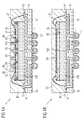
- FIG. 2Aillustrates a stack of integrated circuits according to a further embodiment. Accordingly, stack includes a first integrated circuit 4 and a second integrated circuit 5 .
- the stack of the integrated circuits 4 , 5may be part of or may form another integrated circuit, such as an integrated memory device, an integrated computing device, or an integrated central processing device.
- the stack of the integrated circuitsincludes a first continuous connection from a circuit chip 410 of the first integrated circuit 4 to a lower contact pad 514 on a bottom face 5112 of the substrate 511 of the second integrated circuit 5 .
- This first continuous connectioncouples a chip contact 435 on a top face 4101 of the circuit chip 410 to the lower contact pad 514 , and, includes a contact area 432 on the top face 4101 of the circuit chip 410 , a bond wire 450 , a contact area 412 on a top face 4111 of the substrate 411 of the first integrated circuit 4 , the signal line 413 of the substrate 411 , a lower contact pad 414 on the bottom face 4112 of the substrate 411 of the first integrated circuit 4 , a solder connection 415 , a projecting top contact 540 on a top face 5101 of the circuit chip 510 of the second integrated circuit 5 , a contact area 533 , a signal line 531 , a contact area 532 , a bond wire 550 ,
- the second integrated circuit 5includes a second continuous connection from the circuit chip 510 of the second integrated circuit 5 to a second lower contact pad 518 on the bottom face 5112 of the substrate 511 .
- This second connectionincludes the circuit contact 535 , the contact area 534 , the bond wire 551 , the contact area 516 , the further signal line 517 of the substrate 511 .
- the integrated circuits 4 , 5may be stacked onto each other, or be stacked onto further integrated circuits, while the integrated circuits 4 , 5 may provide a minimum or reduced height of the resulting circuit stack, reducing the overall space, which is required by the stack on a, for example, a circuit board.
- the integrated circuits 4 , 5may also allow for a signal routing from each circuit chip of every constituent integrated circuit of a circuit stack to a common bottom face of the circuit stack.
- a common bottom facemay be provided by the bottom face of a substrate which is part of a bottom integrated circuit, such as the bottom face 5112 of the substrate 511 .
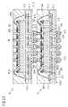
- FIG. 2Billustrates a schematic view of a stack of integrated circuits according to another embodiment.
- a stackincludes the integrated circuit 4 , as this has been described in conjunction with FIG. 2A , and a further integrated circuit 6 .
- a first continuous connection from the circuit chip 410 of the first integrated circuit 4 to a lower contact pad 614 on a bottom face 6112 of the substrate 611 of the second integrated circuit 6includes the contact area 432 , the bond wire 450 , the contact area 412 , the signal line 413 , the lower contact pad 414 , the solder connection 415 , a projecting top contact 640 on a top face 6101 of a circuit chip 610 of the second integrated circuit 6 , a contact area 633 , a signal line 631 , a contact area 632 , a bond wire 650 , a contact area 612 , and a signal line 613 of the substrate 611 .
- a second continuous connection from the circuit chip 610 of the further integrated circuit 6 to a second lower contact pad 618 on the bottom face 6112 of the substrate 611includes a circuit contact 635 , a contact area 634 , a bond wire 651 , a contact area 616 , and a further signal line 617 of the substrate 611 .
- the lower contact pad 414 and further lower contact pads 420 on the bottom face 4112 of the substrate 411are arranged on the bottom face 4112 with a first density of contact pads per area. As illustrated here, a first number of contact pads 414 , 420 is arranged within a fraction 19 of the bottom face 4112 . A density of contacts, contact pads, or solder balls per area may also be denoted as a pitch.
- the lower contact pads 614 , 620 on the bottom face 6112 of the substrate 611are arranged on the bottom face 6112 with a second density of contact pads per area, the second density being less than the first density. Accordingly a lower number of contact pads 614 , 620 is arranged within the corresponding fraction 19 of the bottom face 6112 of the further integrated circuit 6 .
- This lower densitymay also be denoted as a lower pitch.
- different densities and/or pitches of contact pads of the individual integrated circuitsmay be provided, and allow for, for example, a high density interconnection between the individual integrated circuits on one hand, and a connection with a lower density to an external circuit, for example to a circuit board, on the other hand.
- circuit boardsmay be fabricated with substantially reduced requirements to the precision of the process and/or to the purity of involved chemical, gases, and/or environments.
- the contact pads 414 , 420 or 614 , 620may be arranged on respective bottom faces of a substrate in an area under the circuit chip.
- there may be no contact pads outside this areai.e. the area, where there is no circuit chip above on a top face of the substrate may be devoid of any contact pads.
- substrate warpagemay be suppressed or reduced, which may be of advantage if two or several integrated circuits are stacked and coupled to each other.
- the footprint and or area of the integrated circuitmay be reduced or minimized, since no space outside the area of the circuit chip may be required for the placement of contacting or interconnecting contact pads.
- FIG. 3Aillustrates a schematic view of an integrated circuit according to one embodiment.
- an integrated circuit 721includes the circuit chip 10 and the substrate 11 , as they have been described in conjunction with one embodiment.
- a package mold material 60is furthermore arranged on the circuit chip 10 and the substrate 11 .
- the package mold 60provides a top surface 601 on a top face of the integrated circuit 71 .
- the package mold 60exposes a projecting top contact 41 in an area of a top flat 410 of the projecting top contact 41 .
- the top surface 601 of the package mold 60provides a smooth surface in conjunction with the top flat 410 of the projecting top contact 41 .
- a smooth top surface of the integrated circuit 71may be provided with a median variation of top surface level below 100 microns, below 10 microns, or below 1 micron.
- the package mold 60may surround the bond wire 50 , the projecting top contact 41 extending above a maximum height of the bond wire 50 , such that the bond wire 50 is completely encapsuled by the package mold 60 , whereas the package mold 60 still exposes at least the top flat 410 of the projecting top contact 41 .
- FIG. 3Billustrates a schematic view of an integrated circuit according to one embodiment.
- an integrated circuit 72includes the circuit chip 10 on the substrate 11 .
- the package mold 60provides a top face 602 , which exposes projecting top contacts 42 , such that a top section 420 of the projecting top contacts 42 extends above the top face 602 .
- the top sections 420may extend more than 1 micron, more than 10 microns, or more than 100 microns above the top face 602 .
- the projecting and extending top sections 420 of the projecting top contacts 42may provide an increased effective contact surface of the projecting top contacts 42 , such to allow for a reliable and reproducible contacting of the projecting top contacts 42 , by using, for example, a solder ball or a solder connection of or to a further integrated circuit.
- FIG. 3Cillustrates a schematic view of an integrated circuit according to one embodiment.
- An integrated circuit 73includes the circuit chip 10 on the substrate 11 .
- the package mold 60provides a top surface 603 , and seals off parts of the circuit chip 10 and the substrate 11 . Furthermore, the package mold 60 exposes projecting top contacts 43 and provides cavities 6030 in the top face 603 , which are arranged in the area of the projecting top contacts 43 . In this way, the formation of a connection to the projecting top contacts 43 may be guided or enhanced, by using, for example, a guiding of a liquid solder material toward the respective projecting top contact 43 within the cavity 6030 .
- FIG. 3Dillustrates a schematic view of an integrated circuit according to one embodiment.
- An integrated circuit 74includes the circuit chip 10 on a substrate 11 , and a package mold 60 , which, in turn, provides a top surface 604 of the integrated circuit 74 .
- a top cap 440is arranged on a top section of the projecting top contact 44 .
- Such a top cap 440may cover only a top flat of the projecting top contact 44 and/or also a side face of the top section of the projecting top contact 44 .
- the top cap 440may include any top cap of the group of a tin cap, a tin-silver cap, a gold cap, nickel cap, a nickel-gold cap, an organic surface protection cap (OSP), and an organic material cap.
- OSPorganic surface protection cap
- a top section of the projecting top contact 44may be protected for enhancing an establishment of a contact to the projecting top contact 44 by using, for example, a solder connection.
- Reliable and reproducible solder connectionsmay require an inhibiting of an oxidation of the material of the projecting top contact 44 .
- a reproducible and reliable interconnection of more than one integrated circuitmay be provided whilst allowing for a reduction of a reject rade, since, for example, interconnections or solder connections to the projecting top contacts 44 may be established in a reliable and reproducible way.
- the top surface 604may be such as described in conjunction with a previous embodiment, i.e., may provide a smooth surface together with the top cap 440 or top flats of the projecting top contacts 44 , may provide a cavity in the area of the top cap 40 and/or the projecting top contact 44 , or may expose the top cap 440 and/or further parts or the entire projecting top contact 44 such that the top cap 440 and/or a top section of the projecting top contact 44 extends above the top surface 604 .
- a contactmay be established to a top face of a circuit chip which is coupled to a substrate or a carrier by using a bond wire.
- a bond wiremay be bonded to a corresponding contact area, which is also arranged on the top face of the circuit chip.
- the projecting top contactmay bridge the top distance to the circuit chip such to avoid a contact or an interference to the bond wire, which may necessarily extend above the top face of the circuit chip.
- FIGS. 4A through 4Fillustrate schematic views of an integrated circuit in various stages during fabricating, according to yet another embodiment.
- the circuit chip 10is provided, including the contact areas 32 , the signal lines 31 , and the contact areas 33 on the top face 101 of the circuit chip 10 .
- the contact area 32 , the signal line 31 , the contact area 33 , and/or other contact areas and signal linesmay be comprised by the signal distribution layer 30 , which may form or include a redistribution layer (RDL).
- the signal distribution layer 30may, in turn, include additional materials, such as insulating materials and/or layers, such to allow for an insulation of facing or neighboring signal lines 31 , contact areas 33 , and/or contact areas 32 .
- the signal distribution layer 30may include more than one signal routing layer, such to allow for signal line and path crossings without a short connection and/or interference among them.
- the projecting top contacts 40are provided on the top face 101 of the circuit chip 10 .
- the projecting top contacts 40may be provided such to be in contact with the contact areas 33 .
- the projecting top contacts 40may include any of the group of a metal pillar, a copper pillar, a stud bump, a solder ball, and a bond wire stud.
- the provision of the projecting top contact 40may include an electric and/or electroless plating or an electrochemical provision of a metal pillar on the contact area 33 , a liquid fill technique such to provide the projecting top contact 40 on the contact area 33 , a liquid deposition technique such to allow for a provision of a portion of a liquid metal on the contact area 33 , which, after solidification, provides a solid projecting top contact 40 , or a bonding of a bond wire to the contact area 33 , the bond wire being cut such to provide a projecting top contact 40 .
- the circuit chip 10is arranged on the top face 111 of the substrate 11 .
- the circuit chip 10is connected to the substrate 11 , by using the bond wires 50 , which connect the contact areas 32 on the circuit chip 10 to the contact areas 12 , which are arranged, in turn, on the top face 111 of the substrate 11 .
- the provision of the bond wires 50may be such that a maximum height of the bond wires 50 above the top face 111 of the substrate 11 may be lower than a top section of the projecting top contacts 40 . In this way, the projecting top contacts 40 may be contacted to other entities, such as a second integrated circuit, whilst avoiding any contact, damage, interference, or bending of the bond wires 50 .
- the circuit chip 10may be attached to the substrate 11 by using an adhesive material, such as a epoxy resin or a tape.
- a package mold 60is provided on the circuit chip 10 and the substrate 11 .
- the package mold 60may be provided such that the projecting top contacts 40 are covered by the package mold material 60 .
- a package mold 60 and parts of the projecting top contacts 40may be reduced in height, for example by using grinding, chemical mechanical polishing, or polishing processes, such as to expose parts of the projecting top contacts 40 on a top face 600 of the package mold 60 and/or to provide a smooth or uniform surface quality of the top face 600 , as illustrated in FIG. 4E .
- the package mold 60may be provided such to initially provide a common surface 600 with the projecting top contacts 40 , exposing a top section of the projecting top contacts 40 in the area of a cavity of the package mold 60 , or exposing a projecting top section of the projecting top contacts 40 , as described in conjunction with one embodiment, without the need of a reduction of the height, a grinding, or a polishing process of the package mold 60 .
- an integrated circuit 80is provided, which may furthermore include solder balls 15 , solder paste layers, and/or a layer of a solder stop material, such to be suitable for a connection to a circuit board, a connection to a further integrated circuit, or for a stacking in conjunction with several individual integrated circuits.
- a first integrated circuit 81 and a second integrated circuit 82are stacked onto each other.
- the first and second integrated circuits 81 , 82may be manufactured as has been described in conjunction with the integrated circuit 80 in FIGS. 4A through 4E .
- An interconnection of the first integrated circuit 81 to the second integrated circuit 82may be established by using a solder connection 812 , coupling a lower contact pad 811 of the first integrated circuit 81 to a projecting top contact 824 of the second integrated circuit 82 .
- a continuous connection from the circuit chip 10 of the first integrated circuit 81 , or from a top face of the circuit chip 10 of the first integrated circuit 81may be routed to a lower contact pad 821 on the substrate 11 of the second integrated circuit 82 .
- a continuous connection of the circuit chip 10 of the second integrated circuit 82may be routed to a lower contact pad 821 on the substrate 11 of the second integrated circuit 82 .
- the establishing of the continuous connectionsmay be such as described in conjunction with one embodiment.
- a further integrated circuit 83may be stacked on top of the stack of the first integrated circuit 81 and the second integrated circuit 82 . Accordingly, the further integrated circuit 83 may provide a sealed top surface 683 of a package mold 60 , hence covering the circuit chip 10 of the further integrated circuit 83 and providing a sealed off and stable top face of the entire circuit stack. In addition to this, the further integrated circuit 83 may be provided without projecting top contacts, since the further integrated circuit 83 is suitable for forming the top integrated circuit of a stack of several integrated circuits.
- a continuous connection from the circuit chip 10 of the further integrated circuit 83may be formed to a lower contact pad 821 on the substrate 11 of the second integrated circuit 82 , by using routing the signal through the substrate 11 of the further integrated circuit 83 , a projecting top contact 813 on the circuit chip 10 of the first integrated circuit 81 , a surface of the circuit chip 10 of the first integrated circuit 81 , the substrate 11 of the first integrated circuit 81 , a projecting top contact 824 on the circuit chip 10 of the second integrated circuit 82 , a surface of the circuit chip 10 of the second integrated circuit 82 , and the substrate 11 of the second integrated circuit 82 .
- the provision of solder contacts on a substrate outside the chip areamay be avoided, this, in turn, may reduce substrate warpage and the reject rate of integrated circuits during fabrication.
- a package size and/or a foot print of the integrated circuitmay be reduced, and/or a number of input/output ports (IO count) may be increased.
- IO countinput/output ports
- a high grade utilization of the substratemay be provided, due to a reduced package size. This may apply compared to a normal chip scale package (CSP).
- CSPchip scale package
- several chip scale packages with the same scale and/or pitchmay be stacked and connected to each other.
- the package stack heightmay already be reduced for a stack including only two integrated circuits and/or packages.
- a circuit chipmay be or include a flip chip, which is intended to be placed with its top face onto the top face of a substrate or a carrier.
- a flip chipmay be arranged with its bottom face on the top face of the substrate, such that its top face remains accessible and may be contacted to other substrates or chips, and such that a bond wire may be attached to a pad on its top face.
- a high flexibilitymay be provided to cover various ball or bump layouts of the upper circuit, by changing the layout of the projecting top contacts.
Landscapes
- Engineering & Computer Science (AREA)
- Microelectronics & Electronic Packaging (AREA)
- Power Engineering (AREA)
- Computer Hardware Design (AREA)
- Physics & Mathematics (AREA)
- Condensed Matter Physics & Semiconductors (AREA)
- General Physics & Mathematics (AREA)
- Manufacturing & Machinery (AREA)
- Semiconductor Integrated Circuits (AREA)
Abstract
Description
Claims (21)
Priority Applications (1)
| Application Number | Priority Date | Filing Date | Title |
|---|---|---|---|
| US12/032,315US8120186B2 (en) | 2008-02-15 | 2008-02-15 | Integrated circuit and method |
Applications Claiming Priority (1)
| Application Number | Priority Date | Filing Date | Title |
|---|---|---|---|
| US12/032,315US8120186B2 (en) | 2008-02-15 | 2008-02-15 | Integrated circuit and method |
Publications (2)
| Publication Number | Publication Date |
|---|---|
| US20090206461A1 US20090206461A1 (en) | 2009-08-20 |
| US8120186B2true US8120186B2 (en) | 2012-02-21 |
Family
ID=40954333
Family Applications (1)
| Application Number | Title | Priority Date | Filing Date |
|---|---|---|---|
| US12/032,315Active2029-05-01US8120186B2 (en) | 2008-02-15 | 2008-02-15 | Integrated circuit and method |
Country Status (1)
| Country | Link |
|---|---|
| US (1) | US8120186B2 (en) |
Cited By (21)
| Publication number | Priority date | Publication date | Assignee | Title |
|---|---|---|---|---|
| US20110241191A1 (en)* | 2010-03-30 | 2011-10-06 | Takashi Kurogi | Semiconductor lamination package and method of producing semiconductor lamination package |
| US9735084B2 (en) | 2014-12-11 | 2017-08-15 | Invensas Corporation | Bond via array for thermal conductivity |
| US9761554B2 (en) | 2015-05-07 | 2017-09-12 | Invensas Corporation | Ball bonding metal wire bond wires to metal pads |
| US9812402B2 (en) | 2015-10-12 | 2017-11-07 | Invensas Corporation | Wire bond wires for interference shielding |
| US9842745B2 (en) | 2012-02-17 | 2017-12-12 | Invensas Corporation | Heat spreading substrate with embedded interconnects |
| US9888579B2 (en) | 2015-03-05 | 2018-02-06 | Invensas Corporation | Pressing of wire bond wire tips to provide bent-over tips |
| US9911718B2 (en) | 2015-11-17 | 2018-03-06 | Invensas Corporation | ‘RDL-First’ packaged microelectronic device for a package-on-package device |
| US9935075B2 (en) | 2016-07-29 | 2018-04-03 | Invensas Corporation | Wire bonding method and apparatus for electromagnetic interference shielding |
| US9947641B2 (en) | 2014-05-30 | 2018-04-17 | Invensas Corporation | Wire bond support structure and microelectronic package including wire bonds therefrom |
| US9984992B2 (en) | 2015-12-30 | 2018-05-29 | Invensas Corporation | Embedded wire bond wires for vertical integration with separate surface mount and wire bond mounting surfaces |
| US10008469B2 (en) | 2015-04-30 | 2018-06-26 | Invensas Corporation | Wafer-level packaging using wire bond wires in place of a redistribution layer |
| US10062661B2 (en) | 2011-05-03 | 2018-08-28 | Tessera, Inc. | Package-on-package assembly with wire bonds to encapsulation surface |
| US10170412B2 (en) | 2012-05-22 | 2019-01-01 | Invensas Corporation | Substrate-less stackable package with wire-bond interconnect |
| US10181457B2 (en) | 2015-10-26 | 2019-01-15 | Invensas Corporation | Microelectronic package for wafer-level chip scale packaging with fan-out |
| US20190081012A1 (en)* | 2017-09-14 | 2019-03-14 | Shenzhen GOODIX Technology Co., Ltd. | Chip packaging structure and method, and electronic device |
| US10290613B2 (en) | 2013-11-22 | 2019-05-14 | Invensas Corporation | Multiple bond via arrays of different wire heights on a same substrate |
| US10299368B2 (en) | 2016-12-21 | 2019-05-21 | Invensas Corporation | Surface integrated waveguides and circuit structures therefor |
| US10381326B2 (en) | 2014-05-28 | 2019-08-13 | Invensas Corporation | Structure and method for integrated circuits packaging with increased density |
| US10490528B2 (en) | 2015-10-12 | 2019-11-26 | Invensas Corporation | Embedded wire bond wires |
| US11189595B2 (en) | 2011-10-17 | 2021-11-30 | Invensas Corporation | Package-on-package assembly with wire bond vias |
| US11404338B2 (en) | 2014-01-17 | 2022-08-02 | Invensas Corporation | Fine pitch bva using reconstituted wafer with area array accessible for testing |
Families Citing this family (67)
| Publication number | Priority date | Publication date | Assignee | Title |
|---|---|---|---|---|
| KR101313391B1 (en) | 2004-11-03 | 2013-10-01 | 테세라, 인코포레이티드 | Stacked packaging improvements |
| US8058101B2 (en) | 2005-12-23 | 2011-11-15 | Tessera, Inc. | Microelectronic packages and methods therefor |
| US8031475B2 (en)* | 2007-07-12 | 2011-10-04 | Stats Chippac, Ltd. | Integrated circuit package system with flexible substrate and mounded package |
| US8093722B2 (en)* | 2008-05-27 | 2012-01-10 | Mediatek Inc. | System-in-package with fan-out WLCSP |
| US8310051B2 (en) | 2008-05-27 | 2012-11-13 | Mediatek Inc. | Package-on-package with fan-out WLCSP |
| US8278141B2 (en)* | 2008-06-11 | 2012-10-02 | Stats Chippac Ltd. | Integrated circuit package system with internal stacking module |
| US8039303B2 (en) | 2008-06-11 | 2011-10-18 | Stats Chippac, Ltd. | Method of forming stress relief layer between die and interconnect structure |
| US7935570B2 (en)* | 2008-12-10 | 2011-05-03 | Stats Chippac, Ltd. | Semiconductor device and method of embedding integrated passive devices into the package electrically interconnected using conductive pillars |
| US20100167466A1 (en)* | 2008-12-31 | 2010-07-01 | Ravikumar Adimula | Semiconductor package substrate with metal bumps |
| US20100213589A1 (en)* | 2009-02-20 | 2010-08-26 | Tung-Hsien Hsieh | Multi-chip package |
| KR20100112446A (en)* | 2009-04-09 | 2010-10-19 | 삼성전자주식회사 | Stacked semiconductor package and manufacturing method thereof |
| US9355962B2 (en)* | 2009-06-12 | 2016-05-31 | Stats Chippac Ltd. | Integrated circuit package stacking system with redistribution and method of manufacture thereof |
| US20130237055A1 (en)* | 2010-06-11 | 2013-09-12 | Imec | Method of redistributing functional element |
| US8482111B2 (en) | 2010-07-19 | 2013-07-09 | Tessera, Inc. | Stackable molded microelectronic packages |
| US9159708B2 (en)* | 2010-07-19 | 2015-10-13 | Tessera, Inc. | Stackable molded microelectronic packages with area array unit connectors |
| US8378477B2 (en) | 2010-09-14 | 2013-02-19 | Stats Chippac Ltd. | Integrated circuit packaging system with film encapsulation and method of manufacture thereof |
| US8546193B2 (en) | 2010-11-02 | 2013-10-01 | Stats Chippac, Ltd. | Semiconductor device and method of forming penetrable film encapsulant around semiconductor die and interconnect structure |
| KR101075241B1 (en) | 2010-11-15 | 2011-11-01 | 테세라, 인코포레이티드 | Microelectronic package with terminals in dielectric member |
| US20120146206A1 (en) | 2010-12-13 | 2012-06-14 | Tessera Research Llc | Pin attachment |
| US8618659B2 (en) | 2011-05-03 | 2013-12-31 | Tessera, Inc. | Package-on-package assembly with wire bonds to encapsulation surface |
| US8586408B2 (en) | 2011-11-08 | 2013-11-19 | Taiwan Semiconductor Manufacturing Company, Ltd. | Contact and method of formation |
| US8372741B1 (en) | 2012-02-24 | 2013-02-12 | Invensas Corporation | Method for package-on-package assembly with wire bonds to encapsulation surface |
| US9349706B2 (en) | 2012-02-24 | 2016-05-24 | Invensas Corporation | Method for package-on-package assembly with wire bonds to encapsulation surface |
| US9263412B2 (en) | 2012-03-09 | 2016-02-16 | Taiwan Semiconductor Manufacturing Company, Ltd. | Packaging methods and packaged semiconductor devices |
| US20130234317A1 (en)* | 2012-03-09 | 2013-09-12 | Taiwan Semiconductor Manufacturing Company, Ltd. | Packaging Methods and Packaged Semiconductor Devices |
| US8981559B2 (en)* | 2012-06-25 | 2015-03-17 | Taiwan Semiconductor Manufacturing Company, Ltd. | Package on package devices and methods of packaging semiconductor dies |
| US9391008B2 (en) | 2012-07-31 | 2016-07-12 | Invensas Corporation | Reconstituted wafer-level package DRAM |
| US9502390B2 (en) | 2012-08-03 | 2016-11-22 | Invensas Corporation | BVA interposer |
| EP2711977B1 (en)* | 2012-09-19 | 2018-06-13 | ATOTECH Deutschland GmbH | Manufacture of coated copper pillars |
| US8975738B2 (en) | 2012-11-12 | 2015-03-10 | Invensas Corporation | Structure for microelectronic packaging with terminals on dielectric mass |
| US8878353B2 (en) | 2012-12-20 | 2014-11-04 | Invensas Corporation | Structure for microelectronic packaging with bond elements to encapsulation surface |
| US8906743B2 (en)* | 2013-01-11 | 2014-12-09 | Micron Technology, Inc. | Semiconductor device with molded casing and package interconnect extending therethrough, and associated systems, devices, and methods |
| US9378982B2 (en) | 2013-01-31 | 2016-06-28 | Taiwan Semiconductor Manufacturing Company, Ltd. | Die package with openings surrounding end-portions of through package vias (TPVs) and package on package (PoP) using the die package |
| US9136254B2 (en) | 2013-02-01 | 2015-09-15 | Invensas Corporation | Microelectronic package having wire bond vias and stiffening layer |
| US9034696B2 (en) | 2013-07-15 | 2015-05-19 | Invensas Corporation | Microelectronic assemblies having reinforcing collars on connectors extending through encapsulation |
| US8883563B1 (en) | 2013-07-15 | 2014-11-11 | Invensas Corporation | Fabrication of microelectronic assemblies having stack terminals coupled by connectors extending through encapsulation |
| US9023691B2 (en) | 2013-07-15 | 2015-05-05 | Invensas Corporation | Microelectronic assemblies with stack terminals coupled by connectors extending through encapsulation |
| US9768142B2 (en)* | 2013-07-17 | 2017-09-19 | Taiwan Semiconductor Manufacturing Company, Ltd. | Mechanisms for forming bonding structures |
| US9167710B2 (en) | 2013-08-07 | 2015-10-20 | Invensas Corporation | Embedded packaging with preformed vias |
| US9685365B2 (en) | 2013-08-08 | 2017-06-20 | Invensas Corporation | Method of forming a wire bond having a free end |
| US9018645B2 (en)* | 2013-08-29 | 2015-04-28 | Stmicroelectronics Pte Ltd | Optoelectronics assembly and method of making optoelectronics assembly |
| US20150076714A1 (en) | 2013-09-16 | 2015-03-19 | Invensas Corporation | Microelectronic element with bond elements to encapsulation surface |
| US9087815B2 (en) | 2013-11-12 | 2015-07-21 | Invensas Corporation | Off substrate kinking of bond wire |
| US9082753B2 (en) | 2013-11-12 | 2015-07-14 | Invensas Corporation | Severing bond wire by kinking and twisting |
| US9263394B2 (en) | 2013-11-22 | 2016-02-16 | Invensas Corporation | Multiple bond via arrays of different wire heights on a same substrate |
| US9379074B2 (en) | 2013-11-22 | 2016-06-28 | Invensas Corporation | Die stacks with one or more bond via arrays of wire bond wires and with one or more arrays of bump interconnects |
| US9214454B2 (en) | 2014-03-31 | 2015-12-15 | Invensas Corporation | Batch process fabrication of package-on-package microelectronic assemblies |
| US9437577B2 (en)* | 2014-05-09 | 2016-09-06 | Mediatek Inc. | Package on package structure with pillar bump pins and related method thereof |
| US9646917B2 (en) | 2014-05-29 | 2017-05-09 | Invensas Corporation | Low CTE component with wire bond interconnects |
| US9786623B2 (en)* | 2015-03-17 | 2017-10-10 | STATS ChipPAC Pte. Ltd. | Semiconductor device and method of forming PoP semiconductor device with RDL over top package |
| BR112017018820A2 (en)* | 2015-04-14 | 2018-04-24 | Huawei Technologies Co., Ltd. | A chip |
| US9781863B1 (en)* | 2015-09-04 | 2017-10-03 | Microsemi Solutions (U.S.), Inc. | Electronic module with cooling system for package-on-package devices |
| US10332854B2 (en) | 2015-10-23 | 2019-06-25 | Invensas Corporation | Anchoring structure of fine pitch bva |
| US9659848B1 (en) | 2015-11-18 | 2017-05-23 | Invensas Corporation | Stiffened wires for offset BVA |
| US9842820B1 (en)* | 2015-12-04 | 2017-12-12 | Altera Corporation | Wafer-level fan-out wirebond packages |
| US10204893B2 (en) | 2016-05-19 | 2019-02-12 | Invensas Bonding Technologies, Inc. | Stacked dies and methods for forming bonded structures |
| US11276676B2 (en) | 2018-05-15 | 2022-03-15 | Invensas Bonding Technologies, Inc. | Stacked devices and methods of fabrication |
| US11462419B2 (en) | 2018-07-06 | 2022-10-04 | Invensas Bonding Technologies, Inc. | Microelectronic assemblies |
| US11158606B2 (en) | 2018-07-06 | 2021-10-26 | Invensas Bonding Technologies, Inc. | Molded direct bonded and interconnected stack |
| KR102782972B1 (en)* | 2018-07-13 | 2025-03-18 | 삼성전자주식회사 | Memory card and memory card socket |
| KR102650996B1 (en)* | 2018-11-06 | 2024-03-26 | 삼성전자주식회사 | Semiconductor device |
| US11296053B2 (en) | 2019-06-26 | 2022-04-05 | Invensas Bonding Technologies, Inc. | Direct bonded stack structures for increased reliability and improved yield in microelectronics |
| US11393808B2 (en)* | 2019-10-02 | 2022-07-19 | Qualcomm Incorporated | Ultra-low profile stacked RDL semiconductor package |
| TWI715234B (en)* | 2019-10-04 | 2021-01-01 | 瑞昱半導體股份有限公司 | Chip package module |
| TWI713165B (en)* | 2019-11-25 | 2020-12-11 | 南茂科技股份有限公司 | Chip package structure and manufacturing method thereof |
| US11631647B2 (en) | 2020-06-30 | 2023-04-18 | Adeia Semiconductor Bonding Technologies Inc. | Integrated device packages with integrated device die and dummy element |
| CN116097432A (en)* | 2021-09-08 | 2023-05-09 | 华为技术有限公司 | semiconductor package |
Citations (10)
| Publication number | Priority date | Publication date | Assignee | Title |
|---|---|---|---|---|
| DE19845316A1 (en) | 1998-05-30 | 1999-12-02 | Lg Semicon Co Ltd | Stackable ball grid array (BGA) semiconductor casing |
| US6522015B1 (en)* | 2000-09-26 | 2003-02-18 | Amkor Technology, Inc. | Micromachine stacked wirebonded package |
| US20030042591A1 (en)* | 2001-08-30 | 2003-03-06 | Bernd Goller | Electronic component with at least two stacked semiconductor chips, and fabrication method |
| US20030057539A1 (en)* | 2001-09-21 | 2003-03-27 | Michel Koopmans | Bumping technology in stacked die configurations |
| US20040099884A1 (en)* | 2002-11-26 | 2004-05-27 | Fulcher Edwin M. | Thick metal top layer |
| US7185426B1 (en)* | 2002-05-01 | 2007-03-06 | Amkor Technology, Inc. | Method of manufacturing a semiconductor package |
| US20080001271A1 (en)* | 2006-06-30 | 2008-01-03 | Sony Ericsson Mobile Communications Ab | Flipped, stacked-chip IC packaging for high bandwidth data transfer buses |
| US20080012110A1 (en)* | 2006-07-17 | 2008-01-17 | Micron Technology, Inc. | Microelectronic packages with leadframes, including leadframes configured for stacked die packages, and associated systems and methods |
| US20080136003A1 (en)* | 2006-12-07 | 2008-06-12 | Stats Chippac, Inc. | Multi-layer semiconductor package |
| US7550857B1 (en)* | 2006-11-16 | 2009-06-23 | Amkor Technology, Inc. | Stacked redistribution layer (RDL) die assembly package |
- 2008
- 2008-02-15USUS12/032,315patent/US8120186B2/enactiveActive
Patent Citations (11)
| Publication number | Priority date | Publication date | Assignee | Title |
|---|---|---|---|---|
| DE19845316A1 (en) | 1998-05-30 | 1999-12-02 | Lg Semicon Co Ltd | Stackable ball grid array (BGA) semiconductor casing |
| US6291259B1 (en) | 1998-05-30 | 2001-09-18 | Hyundai Electronics Industries Co., Ltd. | Stackable ball grid array semiconductor package and fabrication method thereof |
| US6522015B1 (en)* | 2000-09-26 | 2003-02-18 | Amkor Technology, Inc. | Micromachine stacked wirebonded package |
| US20030042591A1 (en)* | 2001-08-30 | 2003-03-06 | Bernd Goller | Electronic component with at least two stacked semiconductor chips, and fabrication method |
| US20030057539A1 (en)* | 2001-09-21 | 2003-03-27 | Michel Koopmans | Bumping technology in stacked die configurations |
| US7185426B1 (en)* | 2002-05-01 | 2007-03-06 | Amkor Technology, Inc. | Method of manufacturing a semiconductor package |
| US20040099884A1 (en)* | 2002-11-26 | 2004-05-27 | Fulcher Edwin M. | Thick metal top layer |
| US20080001271A1 (en)* | 2006-06-30 | 2008-01-03 | Sony Ericsson Mobile Communications Ab | Flipped, stacked-chip IC packaging for high bandwidth data transfer buses |
| US20080012110A1 (en)* | 2006-07-17 | 2008-01-17 | Micron Technology, Inc. | Microelectronic packages with leadframes, including leadframes configured for stacked die packages, and associated systems and methods |
| US7550857B1 (en)* | 2006-11-16 | 2009-06-23 | Amkor Technology, Inc. | Stacked redistribution layer (RDL) die assembly package |
| US20080136003A1 (en)* | 2006-12-07 | 2008-06-12 | Stats Chippac, Inc. | Multi-layer semiconductor package |
Cited By (35)
| Publication number | Priority date | Publication date | Assignee | Title |
|---|---|---|---|---|
| US20110241191A1 (en)* | 2010-03-30 | 2011-10-06 | Takashi Kurogi | Semiconductor lamination package and method of producing semiconductor lamination package |
| US10593643B2 (en) | 2011-05-03 | 2020-03-17 | Tessera, Inc. | Package-on-package assembly with wire bonds to encapsulation surface |
| US11424211B2 (en) | 2011-05-03 | 2022-08-23 | Tessera Llc | Package-on-package assembly with wire bonds to encapsulation surface |
| US10062661B2 (en) | 2011-05-03 | 2018-08-28 | Tessera, Inc. | Package-on-package assembly with wire bonds to encapsulation surface |
| US11735563B2 (en) | 2011-10-17 | 2023-08-22 | Invensas Llc | Package-on-package assembly with wire bond vias |
| US11189595B2 (en) | 2011-10-17 | 2021-11-30 | Invensas Corporation | Package-on-package assembly with wire bond vias |
| US9842745B2 (en) | 2012-02-17 | 2017-12-12 | Invensas Corporation | Heat spreading substrate with embedded interconnects |
| US10170412B2 (en) | 2012-05-22 | 2019-01-01 | Invensas Corporation | Substrate-less stackable package with wire-bond interconnect |
| US10510659B2 (en) | 2012-05-22 | 2019-12-17 | Invensas Corporation | Substrate-less stackable package with wire-bond interconnect |
| US10629567B2 (en) | 2013-11-22 | 2020-04-21 | Invensas Corporation | Multiple plated via arrays of different wire heights on same substrate |
| USRE49987E1 (en) | 2013-11-22 | 2024-05-28 | Invensas Llc | Multiple plated via arrays of different wire heights on a same substrate |
| US10290613B2 (en) | 2013-11-22 | 2019-05-14 | Invensas Corporation | Multiple bond via arrays of different wire heights on a same substrate |
| US11404338B2 (en) | 2014-01-17 | 2022-08-02 | Invensas Corporation | Fine pitch bva using reconstituted wafer with area array accessible for testing |
| US10381326B2 (en) | 2014-05-28 | 2019-08-13 | Invensas Corporation | Structure and method for integrated circuits packaging with increased density |
| US9947641B2 (en) | 2014-05-30 | 2018-04-17 | Invensas Corporation | Wire bond support structure and microelectronic package including wire bonds therefrom |
| US9735084B2 (en) | 2014-12-11 | 2017-08-15 | Invensas Corporation | Bond via array for thermal conductivity |
| US10806036B2 (en) | 2015-03-05 | 2020-10-13 | Invensas Corporation | Pressing of wire bond wire tips to provide bent-over tips |
| US9888579B2 (en) | 2015-03-05 | 2018-02-06 | Invensas Corporation | Pressing of wire bond wire tips to provide bent-over tips |
| US10008469B2 (en) | 2015-04-30 | 2018-06-26 | Invensas Corporation | Wafer-level packaging using wire bond wires in place of a redistribution layer |
| US9761554B2 (en) | 2015-05-07 | 2017-09-12 | Invensas Corporation | Ball bonding metal wire bond wires to metal pads |
| US10115678B2 (en) | 2015-10-12 | 2018-10-30 | Invensas Corporation | Wire bond wires for interference shielding |
| US11462483B2 (en) | 2015-10-12 | 2022-10-04 | Invensas Llc | Wire bond wires for interference shielding |
| US10490528B2 (en) | 2015-10-12 | 2019-11-26 | Invensas Corporation | Embedded wire bond wires |
| US10559537B2 (en) | 2015-10-12 | 2020-02-11 | Invensas Corporation | Wire bond wires for interference shielding |
| US9812402B2 (en) | 2015-10-12 | 2017-11-07 | Invensas Corporation | Wire bond wires for interference shielding |
| US10181457B2 (en) | 2015-10-26 | 2019-01-15 | Invensas Corporation | Microelectronic package for wafer-level chip scale packaging with fan-out |
| US10043779B2 (en) | 2015-11-17 | 2018-08-07 | Invensas Corporation | Packaged microelectronic device for a package-on-package device |
| US9911718B2 (en) | 2015-11-17 | 2018-03-06 | Invensas Corporation | ‘RDL-First’ packaged microelectronic device for a package-on-package device |
| US9984992B2 (en) | 2015-12-30 | 2018-05-29 | Invensas Corporation | Embedded wire bond wires for vertical integration with separate surface mount and wire bond mounting surfaces |
| US10325877B2 (en) | 2015-12-30 | 2019-06-18 | Invensas Corporation | Embedded wire bond wires for vertical integration with separate surface mount and wire bond mounting surfaces |
| US10658302B2 (en) | 2016-07-29 | 2020-05-19 | Invensas Corporation | Wire bonding method and apparatus for electromagnetic interference shielding |
| US9935075B2 (en) | 2016-07-29 | 2018-04-03 | Invensas Corporation | Wire bonding method and apparatus for electromagnetic interference shielding |
| US10299368B2 (en) | 2016-12-21 | 2019-05-21 | Invensas Corporation | Surface integrated waveguides and circuit structures therefor |
| US10770413B2 (en)* | 2017-09-14 | 2020-09-08 | Shenzhen GOODIX Technology Co., Ltd. | Chip packaging structure and method, and electronic device |
| US20190081012A1 (en)* | 2017-09-14 | 2019-03-14 | Shenzhen GOODIX Technology Co., Ltd. | Chip packaging structure and method, and electronic device |
Also Published As
| Publication number | Publication date |
|---|---|
| US20090206461A1 (en) | 2009-08-20 |
Similar Documents
| Publication | Publication Date | Title |
|---|---|---|
| US8120186B2 (en) | Integrated circuit and method | |
| US7763964B2 (en) | Semiconductor device and semiconductor module using the same | |
| US7598617B2 (en) | Stack package utilizing through vias and re-distribution lines | |
| KR101009121B1 (en) | Microelectronic device having an intermediate contact for connecting to the insert substrate, and a method of packaging a microelectronic device having an intermediate contact | |
| CN111952274B (en) | Electronic package and manufacturing method thereof | |
| US8283767B1 (en) | Dual laminate package structure with embedded elements | |
| US7242081B1 (en) | Stacked package structure | |
| TWI671861B (en) | Semiconductor package structure and method of making the same | |
| US6812567B2 (en) | Semiconductor package and package stack made thereof | |
| US7948089B2 (en) | Chip stack package and method of fabricating the same | |
| US12255182B2 (en) | Electronic package and manufacturing method thereof | |
| CN115312487B (en) | Electronic packaging and manufacturing method thereof | |
| US8008765B2 (en) | Semiconductor package having adhesive layer and method of manufacturing the same | |
| CN114628340B (en) | Electronic packaging and method of manufacturing the same | |
| EP2880684B1 (en) | Microelectronic assembly | |
| CN100524741C (en) | Stacked package structure | |
| TWI766192B (en) | Electronic package and method for manufacturing the same | |
| TWI723414B (en) | Electronic package and manufacturing method thereof | |
| CN118039572A (en) | Electronic package and method for manufacturing the same | |
| CN115579298A (en) | Chip packaging method and packaged chip | |
| TW202336970A (en) | Electronic package and manufacturing method thereof | |
| US20240145455A1 (en) | Electronic package and manufacturing method thereof | |
| TWI823618B (en) | Electronic package | |
| US20230111207A1 (en) | Semiconductor package including sub-package | |
| KR20010063236A (en) | Stack package and manufacturing method thereof |
Legal Events
| Date | Code | Title | Description |
|---|---|---|---|
| AS | Assignment | Owner name:QIMONDA AG, GERMANY Free format text:ASSIGNMENT OF ASSIGNORS INTEREST;ASSIGNOR:YOON, KIMYUNG;REEL/FRAME:020932/0255 Effective date:20080220 | |
| FEPP | Fee payment procedure | Free format text:PAYOR NUMBER ASSIGNED (ORIGINAL EVENT CODE: ASPN); ENTITY STATUS OF PATENT OWNER: LARGE ENTITY | |
| STCF | Information on status: patent grant | Free format text:PATENTED CASE | |
| FEPP | Fee payment procedure | Free format text:PAT HOLDER NO LONGER CLAIMS SMALL ENTITY STATUS, ENTITY STATUS SET TO UNDISCOUNTED (ORIGINAL EVENT CODE: STOL); ENTITY STATUS OF PATENT OWNER: LARGE ENTITY | |
| AS | Assignment | Owner name:INFINEON TECHNOLOGIES AG, GERMANY Free format text:ASSIGNMENT OF ASSIGNORS INTEREST;ASSIGNOR:QIMONDA AG;REEL/FRAME:035623/0001 Effective date:20141009 | |
| FPAY | Fee payment | Year of fee payment:4 | |
| AS | Assignment | Owner name:POLARIS INNOVATIONS LIMITED, IRELAND Free format text:ASSIGNMENT OF ASSIGNORS INTEREST;ASSIGNOR:INFINEON TECHNOLOGIES AG;REEL/FRAME:036575/0670 Effective date:20150708 | |
| MAFP | Maintenance fee payment | Free format text:PAYMENT OF MAINTENANCE FEE, 8TH YEAR, LARGE ENTITY (ORIGINAL EVENT CODE: M1552); ENTITY STATUS OF PATENT OWNER: LARGE ENTITY Year of fee payment:8 | |
| MAFP | Maintenance fee payment | Free format text:PAYMENT OF MAINTENANCE FEE, 12TH YEAR, LARGE ENTITY (ORIGINAL EVENT CODE: M1553); ENTITY STATUS OF PATENT OWNER: LARGE ENTITY Year of fee payment:12 |