US8120134B2 - High-performance diode device structure and materials used for the same - Google Patents
High-performance diode device structure and materials used for the sameDownload PDFInfo
- Publication number
- US8120134B2 US8120134B2US12/580,013US58001309AUS8120134B2US 8120134 B2US8120134 B2US 8120134B2US 58001309 AUS58001309 AUS 58001309AUS 8120134 B2US8120134 B2US 8120134B2
- Authority
- US
- United States
- Prior art keywords
- diode
- resistivity
- memory device
- decrease
- memory
- Prior art date
- Legal status (The legal status is an assumption and is not a legal conclusion. Google has not performed a legal analysis and makes no representation as to the accuracy of the status listed.)
- Active, expires
Links
- 239000000463materialSubstances0.000titleclaimsabstractdescription86
- 230000007423decreaseEffects0.000claimsabstractdescription14
- 230000004044responseEffects0.000claimsabstractdescription4
- 238000010438heat treatmentMethods0.000claimsdescription20
- 239000004020conductorSubstances0.000claimsdescription11
- XHCLAFWTIXFWPH-UHFFFAOYSA-N[O-2].[O-2].[O-2].[O-2].[O-2].[V+5].[V+5]Chemical compound[O-2].[O-2].[O-2].[O-2].[O-2].[V+5].[V+5]XHCLAFWTIXFWPH-UHFFFAOYSA-N0.000claimsdescription7
- 229910001935vanadium oxideInorganic materials0.000claimsdescription7
- 229910052761rare earth metalInorganic materials0.000claimsdescription6
- 229910000473manganese(VI) oxideInorganic materials0.000claimsdescription5
- -1rare earth manganateChemical class0.000claimsdescription4
- 238000000034methodMethods0.000description12
- 229910052751metalInorganic materials0.000description7
- 239000002184metalSubstances0.000description7
- XUIMIQQOPSSXEZ-UHFFFAOYSA-NSiliconChemical compound[Si]XUIMIQQOPSSXEZ-UHFFFAOYSA-N0.000description6
- 230000005684electric fieldEffects0.000description6
- 229910052710siliconInorganic materials0.000description6
- 239000010703siliconSubstances0.000description6
- 230000007704transitionEffects0.000description6
- 239000012212insulatorSubstances0.000description4
- 238000004519manufacturing processMethods0.000description3
- PXHVJJICTQNCMI-UHFFFAOYSA-NNickelChemical compound[Ni]PXHVJJICTQNCMI-UHFFFAOYSA-N0.000description2
- 238000000231atomic layer depositionMethods0.000description2
- 238000005229chemical vapour depositionMethods0.000description2
- 230000000694effectsEffects0.000description2
- 230000002349favourable effectEffects0.000description2
- 230000006870functionEffects0.000description2
- 238000000059patterningMethods0.000description2
- BASFCYQUMIYNBI-UHFFFAOYSA-NplatinumChemical compound[Pt]BASFCYQUMIYNBI-UHFFFAOYSA-N0.000description2
- 150000002910rare earth metalsChemical class0.000description2
- 239000004065semiconductorSubstances0.000description2
- 229910021332silicideInorganic materials0.000description2
- 229910052715tantalumInorganic materials0.000description2
- GUVRBAGPIYLISA-UHFFFAOYSA-Ntantalum atomChemical compound[Ta]GUVRBAGPIYLISA-UHFFFAOYSA-N0.000description2
- WFKWXMTUELFFGS-UHFFFAOYSA-NtungstenChemical compound[W]WFKWXMTUELFFGS-UHFFFAOYSA-N0.000description2
- 229910052721tungstenInorganic materials0.000description2
- 239000010937tungstenSubstances0.000description2
- RYGMFSIKBFXOCR-UHFFFAOYSA-NCopperChemical compound[Cu]RYGMFSIKBFXOCR-UHFFFAOYSA-N0.000description1
- ZOKXTWBITQBERF-UHFFFAOYSA-NMolybdenumChemical compound[Mo]ZOKXTWBITQBERF-UHFFFAOYSA-N0.000description1
- BPQQTUXANYXVAA-UHFFFAOYSA-NOrthosilicateChemical compound[O-][Si]([O-])([O-])[O-]BPQQTUXANYXVAA-UHFFFAOYSA-N0.000description1
- RTAQQCXQSZGOHL-UHFFFAOYSA-NTitaniumChemical compound[Ti]RTAQQCXQSZGOHL-UHFFFAOYSA-N0.000description1
- 229910052782aluminiumInorganic materials0.000description1
- XAGFODPZIPBFFR-UHFFFAOYSA-NaluminiumChemical compound[Al]XAGFODPZIPBFFR-UHFFFAOYSA-N0.000description1
- 238000003491arrayMethods0.000description1
- 230000009286beneficial effectEffects0.000description1
- 230000008859changeEffects0.000description1
- 229910052802copperInorganic materials0.000description1
- 239000010949copperSubstances0.000description1
- 238000000151depositionMethods0.000description1
- 230000008021depositionEffects0.000description1
- 238000005530etchingMethods0.000description1
- 238000001704evaporationMethods0.000description1
- 230000008020evaporationEffects0.000description1
- 230000001747exhibiting effectEffects0.000description1
- PCHJSUWPFVWCPO-UHFFFAOYSA-NgoldChemical compound[Au]PCHJSUWPFVWCPO-UHFFFAOYSA-N0.000description1
- 229910052737goldInorganic materials0.000description1
- 239000010931goldSubstances0.000description1
- 229910044991metal oxideInorganic materials0.000description1
- 150000004706metal oxidesChemical class0.000description1
- 150000002739metalsChemical class0.000description1
- 239000000203mixtureSubstances0.000description1
- 230000004048modificationEffects0.000description1
- 238000012986modificationMethods0.000description1
- 229910052750molybdenumInorganic materials0.000description1
- 239000011733molybdenumSubstances0.000description1
- 229910052759nickelInorganic materials0.000description1
- 150000004767nitridesChemical class0.000description1
- 230000002093peripheral effectEffects0.000description1
- 238000000623plasma-assisted chemical vapour depositionMethods0.000description1
- 229910052697platinumInorganic materials0.000description1
- 230000008569processEffects0.000description1
- FVBUAEGBCNSCDD-UHFFFAOYSA-Nsilicide(4-)Chemical compound[Si-4]FVBUAEGBCNSCDD-UHFFFAOYSA-N0.000description1
- 238000004544sputter depositionMethods0.000description1
- 238000006467substitution reactionMethods0.000description1
- 239000000758substrateSubstances0.000description1
- 238000002207thermal evaporationMethods0.000description1
- 239000010409thin filmSubstances0.000description1
- 239000010936titaniumSubstances0.000description1
- 229910052719titaniumInorganic materials0.000description1
- 238000007740vapor depositionMethods0.000description1
Images


Classifications
- H—ELECTRICITY
- H10—SEMICONDUCTOR DEVICES; ELECTRIC SOLID-STATE DEVICES NOT OTHERWISE PROVIDED FOR
- H10B—ELECTRONIC MEMORY DEVICES
- H10B63/00—Resistance change memory devices, e.g. resistive RAM [ReRAM] devices
- H—ELECTRICITY
- H10—SEMICONDUCTOR DEVICES; ELECTRIC SOLID-STATE DEVICES NOT OTHERWISE PROVIDED FOR
- H10D—INORGANIC ELECTRIC SEMICONDUCTOR DEVICES
- H10D62/00—Semiconductor bodies, or regions thereof, of devices having potential barriers
- H10D62/80—Semiconductor bodies, or regions thereof, of devices having potential barriers characterised by the materials
- H—ELECTRICITY
- H10—SEMICONDUCTOR DEVICES; ELECTRIC SOLID-STATE DEVICES NOT OTHERWISE PROVIDED FOR
- H10N—ELECTRIC SOLID-STATE DEVICES NOT OTHERWISE PROVIDED FOR
- H10N70/00—Solid-state devices having no potential barriers, and specially adapted for rectifying, amplifying, oscillating or switching
Definitions
- Diodesare one of the most fundamental semiconductor elements or components.
- a diodeusually allows current flow in one direction but not in another.
- a diodeis constructed as a two-region device separated by a junction; however, various types of diodes which have different junction structures also exist.
- Two examples of common diode typesinclude silicon-based doped p-n junction diodes and Schottky diodes.
- Diodeshave many applications and are frequently used in, for example, memory devices, logic circuits or solar cells, or may function as LEDs (light emitting diodes). Diode devices with high ON current and high ON/OFF current ratio (resulting in low leakage current) also have many applications, such as for example, as a select device in a memory element. Silicon-based junction diodes may provide high ON current and high ON/OFF current ratios, but the manufacturing process of conventional silicon-based junction diodes is much more complicated and requires higher processing temperatures than, for example, a metal-insulator-metal (MIM) diode system. Unfortunately, known MIM diode systems are not able to meet the high forward current requirements of many applications.
- MIMmetal-insulator-metal
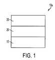
- FIG. 1is a cross-sectional view of a diode according to a disclosed embodiment.
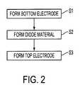
- FIG. 2is a flowchart illustrating a manufacturing method for a diode according to FIG. 1 .
- FIG. 3is an I-V curve of a diode according to a disclosed embodiment.
- FIG. 4is a cross-sectional view of a diode according to another disclosed embodiment.
- FIG. 5Aillustrates a cross-sectional view of a cross point memory device including a diode according to a disclosed embodiment.
- FIG. 5Billustrates a top view of the cross point memory device of FIG. 5A .
- FIG. 6is an I-V curve of a diode included in a memory device according to a disclosed embodiment.
- FIG. 7illustrates a processing system, utilizing a diode and/or memory device according to a disclosed embodiment.
- Disclosed embodimentsrelate to a diode device and methods of constructing and operating the same, wherein the diode exhibits high ON current as well as a high ON/OFF ratio. Disclosed embodiments achieve these characteristics by using a combination of the properties of low electric field turn-on and joule assisted self heating to build high forward currents at relatively low voltage values.
- the embodimentsutilize a material that has a first characteristic allowing a first decrease in a resistivity of the material upon application of a low voltage and a second characteristic allowing a second decrease in the resistivity of the material in response to an increase in temperature of the material.
- Diode 10 aincludes conductive materials 15 and 25 on either side of material 20 (described below in more detail). Conductive materials 15 and 25 may also be referred to as diode electrodes. Referring to FIG. 2 , the example embodiment of FIG. 1 may be fabricated as follows. Conductive material 15 may be formed over any suitable substrate base (not shown), at step S 1 . Conductive material 15 may be patterned as desired by utilizing photolithographic processing and one or more etches, or by any other suitable patterning technique. Material 20 may then be formed over conductive material 15 , at step S 2 .
- material 20may be deposited on material 15 and may then be patterned using photolithographic processing and one or more etches, or by any other suitable patterning technique.
- Material 20may be deposited with any suitable methodology, including, for example, atomic layer deposition (ALD) methods or plasma vapor deposition (PVD) methods, such as sputtering and evaporation, thermal deposition, chemical vapor deposition (CVD) methods, plasma-enhanced (PECVD) methods, and photo-organic deposition (PODM).
- Conductive material 25may then be deposited over material 20 , at step S 3 , using one or more of the techniques described above in relation to material 20 , or any other method.
- Each of conductive materials 15 and 25 and the material 20may be formed as thin-films.
- diode 10 amay be formed by layering all of the materials 15 , 20 and 25 and then etching them all at once to form a diode stack.
- Conductive materials 15 and 25may include any suitable conductive material, such as, for example, one or more of various metals, such as tantalum, platinum, tungsten, aluminum, copper, gold, nickel, titanium, molybdenum, etc., metal-containing compositions, such as metal nitrides, metal silicides (e.g., tungsten silicate or tantalum silicide, etc.), and conductively-doped semiconductor materials (for instance, conductively-doped silicon). Additionally, conductive materials 15 and 25 may be formed of the same material or of different materials.
- various metalssuch as tantalum, platinum, tungsten, aluminum, copper, gold, nickel, titanium, molybdenum, etc.
- metal-containing compositionssuch as metal nitrides, metal silicides (e.g., tungsten silicate or tantalum silicide, etc.), and conductively-doped semiconductor materials (for instance, conductively-doped silicon).
- conductive materials 15 and 25may
- Material 20is selected such that under initial programming (off) conditions, current is not conducted from material 25 to material 15 , but that under appropriate operating conditions, the material 20 undergoes a transition and becomes conductive.
- Appropriate materials selected for material 20are those that operate in a fashion similar to the operation illustrated in the I-V curve of FIG. 3 . There are two separate phenomena at work in conjunction with each other to allow the particular curve profile shown in FIG. 3 to be achieved. These phenomena are low electric field assisted metal-insulator transition and Joule heating assisted current increase.
- Low electric field assisted metal-insulator transitionoccurs in materials whose resistance is changed when a voltage is applied to the material. While the voltage remains below a threshold voltage value (V th ), material 20 has a high resistivity. When the voltage reaches the threshold voltage value (V th ), however, material 20 quickly changes to a low resistivity. Joule heating assisted current increase occurs when, due to the temperature increase of the material resulting from the heat generated by the current flowing through the material, the resistivity of the material suddenly decreases, allowing a corresponding sudden increase in current flow.
- an appropriate material for material 20will have a low threshold voltage (V th ) and allow high forward current (A) to the diode at relatively low voltages.
- V ththreshold voltage
- Aforward current
- the threshold voltagepreferably occurs at a voltage value of approximately 0.5V to approximately 1.5V and this is preferably observed at room temperature.
- the Joule heating assisted current increasepreferably occurs at voltage values of approximately 4.0V or below (e.g., between approximately 1.5V and approximately 4.0V).
- FIG. 3should not be taken as a precise representation of an I-V curve according to disclosed embodiments but should only be taken as an approximation of a representative typical temperature profile according to one the disclosed embodiments.
- FIG. 3should not be interpreted as a limitation on the scope of all embodiments.
- this combination of multiple steep current increasesallows very high forward current drive at a relatively low voltage and a relatively low current at voltages below the threshold voltage, resulting in a high performance diode device having an ultra high forward current density (e.g., between approximately 1 ⁇ 10 6 A/cm 2 to approximately 1 ⁇ 10 8 A/cm 2 , and preferably on the order of 1 ⁇ 10 7 A/cm 2 ) and a very high ON/OFF current ratio.
- the I-V curves of the diode of the disclosed embodimentsare non-ohmic and the change in the resistivity over the curve can be several orders of magnitude (>10 5 ).
- material 20In order to achieve such a beneficial result from the low electric field assisted metal-insulator transition and Joule heating assisted current increase, material 20 must be chosen to be compatible with each of these effects.
- a heating elementmay additionally be included in the diode in order to assist with the temperature increase, thus more easily reaching the temperature at which the current increases for the second time.
- Thisis illustrated in the diode 10 b of FIG. 4 , which further includes heating element 28 between electrode 15 and material 20 .
- the heating element 28may be positioned between material 20 and electrode 25 or two heating elements 28 may be included, one positioned between electrode 15 and material 20 and the other positioned between material 20 and electrode 25 .
- Heating element 28is formed of any material having a suitable resistance to cause the desired amount of heating when current flows through the material while still allowing current flow through the diode, such as for example metal oxides.
- Heating element 28may also be, for example, a metal heating coil.
- Other elements of FIG. 4are the same as described with respect to FIG. 1 .
- Diodes of the disclosed embodimentsmay be used in any application requiring a diode, and in particular one in which high forward current density is desired. Examples include memory applications, logic circuits, solar cells, or LEDs.
- One example application particularly suited to the diodes of the disclosed embodimentsis a select device for a cross point memory device 100 , as illustrated for example in FIGS. 5A and 5B .
- FIG. 5Aillustrates a cross-sectional view of a cross point memory device 100 including a diode 10 a ( FIG. 1 ).
- diode 10 bFIG. 4
- FIG. 5Billustrates a top view of the cross point memory device 100 .
- the access lines 110for example word lines, and data/sense lines 120 , for example bit lines, of the cross point memory device 100 are connected at their intersections by a diode 10 a of the disclosed embodiments.
- word line 110operates as the diode electrode 15 ( FIG. 1 ) and electrode 150 operates as diode electrode 25 ( FIG. 1 ).
- Memory element 140is present above electrode 150 and is accessed via the diode 10 a .
- the memory element 140may be “read” and after the second increase in current, the “write” function may be performed.
- FIG. 7illustrates a simplified processor system 700 , which includes a memory device 702 which may include memory array 100 (and diode 10 a , 10 b ) in accordance with the above described embodiments.
- a processor systemsuch as a computer system, generally comprises a central processing unit (CPU) 710 , such as a microprocessor, a digital signal processor, or other programmable digital logic devices, which communicates with input/output (I/O) devices 720 over a bus 790 .
- the memory device 702communicates with the CPU 710 over bus 790 typically through a memory controller.
- the processor system 700may also include flash memory 760 .
- the processor system 700may include peripheral devices such as removable media devices 750 (e.g., CD-ROM drive or DVD drive) which communicate with CPU 710 over the bus 790 .
- Memory device 702can be constructed as an integrated circuit, which includes one or more memory arrays 100 and/or diodes 10 a , 10 b . If desired, the memory device 702 may be combined with the processor, for example CPU 710 , as a single integrated circuit.
Landscapes
- Semiconductor Memories (AREA)
Abstract
Description
Claims (20)
Priority Applications (3)
| Application Number | Priority Date | Filing Date | Title |
|---|---|---|---|
| US12/580,013US8120134B2 (en) | 2009-10-15 | 2009-10-15 | High-performance diode device structure and materials used for the same |
| US13/352,833US8476140B2 (en) | 2009-10-15 | 2012-01-18 | High-performance diode device structure and materials used for the same |
| US13/929,094US8796806B2 (en) | 2009-10-15 | 2013-06-27 | High-performance diode device structure and materials used for the same |
Applications Claiming Priority (1)
| Application Number | Priority Date | Filing Date | Title |
|---|---|---|---|
| US12/580,013US8120134B2 (en) | 2009-10-15 | 2009-10-15 | High-performance diode device structure and materials used for the same |
Related Child Applications (1)
| Application Number | Title | Priority Date | Filing Date |
|---|---|---|---|
| US13/352,833DivisionUS8476140B2 (en) | 2009-10-15 | 2012-01-18 | High-performance diode device structure and materials used for the same |
Publications (2)
| Publication Number | Publication Date |
|---|---|
| US20110089413A1 US20110089413A1 (en) | 2011-04-21 |
| US8120134B2true US8120134B2 (en) | 2012-02-21 |
Family
ID=43878609
Family Applications (3)
| Application Number | Title | Priority Date | Filing Date |
|---|---|---|---|
| US12/580,013Active2030-02-10US8120134B2 (en) | 2009-10-15 | 2009-10-15 | High-performance diode device structure and materials used for the same |
| US13/352,833ActiveUS8476140B2 (en) | 2009-10-15 | 2012-01-18 | High-performance diode device structure and materials used for the same |
| US13/929,094ActiveUS8796806B2 (en) | 2009-10-15 | 2013-06-27 | High-performance diode device structure and materials used for the same |
Family Applications After (2)
| Application Number | Title | Priority Date | Filing Date |
|---|---|---|---|
| US13/352,833ActiveUS8476140B2 (en) | 2009-10-15 | 2012-01-18 | High-performance diode device structure and materials used for the same |
| US13/929,094ActiveUS8796806B2 (en) | 2009-10-15 | 2013-06-27 | High-performance diode device structure and materials used for the same |
Country Status (1)
| Country | Link |
|---|---|
| US (3) | US8120134B2 (en) |
Cited By (1)
| Publication number | Priority date | Publication date | Assignee | Title |
|---|---|---|---|---|
| US8796806B2 (en)* | 2009-10-15 | 2014-08-05 | Micron Technology, Inc. | High-performance diode device structure and materials used for the same |
Families Citing this family (4)
| Publication number | Priority date | Publication date | Assignee | Title |
|---|---|---|---|---|
| EP2597647A1 (en)* | 2011-11-28 | 2013-05-29 | Imec | Selector device for memory applications |
| WO2015084810A2 (en) | 2013-12-05 | 2015-06-11 | The Board Of Regents Of The University Of Oklahoma | Thermophotovoltaic materials, methods of deposition, and devices |
| TWI571754B (en)* | 2015-02-02 | 2017-02-21 | 群暉科技股份有限公司 | Method for performing file synchronization control, and associated apparatus |
| DE102018112605A1 (en) | 2018-05-25 | 2019-11-28 | Helmholtz-Zentrum Dresden - Rossendorf E.V. | A method of reconfiguring a vortex density in a rare earth manganate, a nonvolatile impedance switch and its use |
Citations (11)
| Publication number | Priority date | Publication date | Assignee | Title |
|---|---|---|---|---|
| US4839219A (en) | 1986-05-20 | 1989-06-13 | Kanegafuchi Kagaku Kogyo Kabushiki Kaisha | Thin film and device having the same |
| US5614727A (en) | 1995-06-06 | 1997-03-25 | International Business Machines Corporation | Thin film diode having large current capability with low turn-on voltages for integrated devices |
| US5625587A (en)* | 1995-07-12 | 1997-04-29 | Virginia Polytechnic Institute And State University | Rare earth manganate films made by metalorganic decomposition or metalorganic chemical vapor deposition for nonvolatile memory devices |
| US6087702A (en) | 1997-11-26 | 2000-07-11 | National Science Council | Rare-earth schottky diode structure |
| US20050191776A1 (en)* | 2002-06-26 | 2005-09-01 | 3M Innovative Properties Company | Buffer layers for organic electroluminescent devices and methods of manufacture and use |
| US20050265072A1 (en)* | 2004-05-28 | 2005-12-01 | Hart Mark W | Indirect switching and sensing of phase change memory cells |
| US7361406B2 (en) | 2003-04-29 | 2008-04-22 | Qi Wang | Ultra-high current density thin-film Si diode |
| US20080105870A1 (en) | 2006-11-07 | 2008-05-08 | Cbrite Inc. | Two-terminal switching devices and their methods of fabrication |
| US20080272363A1 (en) | 2007-05-01 | 2008-11-06 | Chandra Mouli | Selectively Conducting Devices, Diode Constructions, Constructions, and Diode Forming Methods |
| US20080316809A1 (en) | 2007-06-25 | 2008-12-25 | Sandisk 3D Llc | High forward current diodes for reverse write 3D cell |
| US20090072246A1 (en) | 2007-09-18 | 2009-03-19 | Samsung Electronics Co., Ltd. | Diode and memory device comprising the same |
Family Cites Families (4)
| Publication number | Priority date | Publication date | Assignee | Title |
|---|---|---|---|---|
| US3822381A (en)* | 1971-03-08 | 1974-07-02 | Wisconsin Alumni Res Found | Multimode oscillators for pattern recognition |
| US5912791A (en)* | 1997-03-14 | 1999-06-15 | Seagate Technology, Inc. | Landing zone design for a magnetic disc |
| EP2546192B1 (en)* | 2005-02-16 | 2019-12-18 | Massachusetts Institute Of Technology | Light emitting device including semiconductor nanocrystals |
| US8120134B2 (en)* | 2009-10-15 | 2012-02-21 | Micron Technology, Inc. | High-performance diode device structure and materials used for the same |
- 2009
- 2009-10-15USUS12/580,013patent/US8120134B2/enactiveActive
- 2012
- 2012-01-18USUS13/352,833patent/US8476140B2/enactiveActive
- 2013
- 2013-06-27USUS13/929,094patent/US8796806B2/enactiveActive
Patent Citations (12)
| Publication number | Priority date | Publication date | Assignee | Title |
|---|---|---|---|---|
| US4839219A (en) | 1986-05-20 | 1989-06-13 | Kanegafuchi Kagaku Kogyo Kabushiki Kaisha | Thin film and device having the same |
| US5614727A (en) | 1995-06-06 | 1997-03-25 | International Business Machines Corporation | Thin film diode having large current capability with low turn-on voltages for integrated devices |
| US5625587A (en)* | 1995-07-12 | 1997-04-29 | Virginia Polytechnic Institute And State University | Rare earth manganate films made by metalorganic decomposition or metalorganic chemical vapor deposition for nonvolatile memory devices |
| US6087702A (en) | 1997-11-26 | 2000-07-11 | National Science Council | Rare-earth schottky diode structure |
| US20050191776A1 (en)* | 2002-06-26 | 2005-09-01 | 3M Innovative Properties Company | Buffer layers for organic electroluminescent devices and methods of manufacture and use |
| US7361406B2 (en) | 2003-04-29 | 2008-04-22 | Qi Wang | Ultra-high current density thin-film Si diode |
| US20050265072A1 (en)* | 2004-05-28 | 2005-12-01 | Hart Mark W | Indirect switching and sensing of phase change memory cells |
| US7009694B2 (en)* | 2004-05-28 | 2006-03-07 | International Business Machines Corporation | Indirect switching and sensing of phase change memory cells |
| US20080105870A1 (en) | 2006-11-07 | 2008-05-08 | Cbrite Inc. | Two-terminal switching devices and their methods of fabrication |
| US20080272363A1 (en) | 2007-05-01 | 2008-11-06 | Chandra Mouli | Selectively Conducting Devices, Diode Constructions, Constructions, and Diode Forming Methods |
| US20080316809A1 (en) | 2007-06-25 | 2008-12-25 | Sandisk 3D Llc | High forward current diodes for reverse write 3D cell |
| US20090072246A1 (en) | 2007-09-18 | 2009-03-19 | Samsung Electronics Co., Ltd. | Diode and memory device comprising the same |
Non-Patent Citations (2)
| Title |
|---|
| Myoung-Jae Lee, et al., "Low-Temperature-Grown Transition Metal Oxide Based Storage Materials and Oxide Transistors for High-Density Non-volatile Memory", (Research paper), http://www3.interscience.wiley.com/journal/121544710/abstract, Published on-line Dec. 4, 2008. |
| Z.G. Sheng, et al., "Transport Properties and Backward Diode-like Behavior in Manganite-Based P-I-N Junctions," J. Phys. D: Appl. Phys. 41 1350089 (Jun. 19, 2008). |
Cited By (1)
| Publication number | Priority date | Publication date | Assignee | Title |
|---|---|---|---|---|
| US8796806B2 (en)* | 2009-10-15 | 2014-08-05 | Micron Technology, Inc. | High-performance diode device structure and materials used for the same |
Also Published As
| Publication number | Publication date |
|---|---|
| US20120112185A1 (en) | 2012-05-10 |
| US20140014946A1 (en) | 2014-01-16 |
| US8476140B2 (en) | 2013-07-02 |
| US8796806B2 (en) | 2014-08-05 |
| US20110089413A1 (en) | 2011-04-21 |
Similar Documents
| Publication | Publication Date | Title |
|---|---|---|
| JP5154138B2 (en) | Variable resistance random access memory device with n + interface layer | |
| US7816659B2 (en) | Devices having reversible resistivity-switching metal oxide or nitride layer with added metal | |
| US8067815B2 (en) | Aluminum copper oxide based memory devices and methods for manufacture | |
| US8724369B2 (en) | Composition of memory cell with resistance-switching layers | |
| US8847188B2 (en) | Switching device and memory device including the same | |
| CN103168372B (en) | There is the combination of the memory cell of resistance switch layer | |
| US20070015348A1 (en) | Crosspoint resistor memory device with back-to-back Schottky diodes | |
| US9019747B2 (en) | Nonvolatile semiconductor memory device and write method for the same | |
| US8796806B2 (en) | High-performance diode device structure and materials used for the same | |
| TW201138088A (en) | Punch-through diode steering element | |
| US9252189B2 (en) | Nonvolatile semiconductor memory element, nonvolatile semiconductor memory device, and method for manufacturing nonvolatile semiconductor memory device | |
| US9368196B2 (en) | Semiconductor memory device | |
| WO2010004675A1 (en) | Current reduction element, memory element, and methods for manufacture of the elements | |
| US20250194108A1 (en) | Rram process integration scheme and cell structure with reduced masking operations | |
| US20120168706A1 (en) | Resistance random access memory | |
| JP2007158325A (en) | Crosspoint resistive memory device with bidirectional Schottky diode | |
| US20170062522A1 (en) | Combining Materials in Different Components of Selector Elements of Integrated Circuits |
Legal Events
| Date | Code | Title | Description |
|---|---|---|---|
| AS | Assignment | Owner name:MICRON TECHNOLOGY, INC., IDAHO Free format text:ASSIGNMENT OF ASSIGNORS INTEREST;ASSIGNORS:SANDHU, GURTEJ;SRINIVASAN, BHASKAR;SIGNING DATES FROM 20090924 TO 20091005;REEL/FRAME:023381/0468 | |
| FEPP | Fee payment procedure | Free format text:PAYOR NUMBER ASSIGNED (ORIGINAL EVENT CODE: ASPN); ENTITY STATUS OF PATENT OWNER: LARGE ENTITY | |
| STCF | Information on status: patent grant | Free format text:PATENTED CASE | |
| CC | Certificate of correction | ||
| FPAY | Fee payment | Year of fee payment:4 | |
| AS | Assignment | Owner name:U.S. BANK NATIONAL ASSOCIATION, AS COLLATERAL AGENT, CALIFORNIA Free format text:SECURITY INTEREST;ASSIGNOR:MICRON TECHNOLOGY, INC.;REEL/FRAME:038669/0001 Effective date:20160426 Owner name:U.S. BANK NATIONAL ASSOCIATION, AS COLLATERAL AGEN Free format text:SECURITY INTEREST;ASSIGNOR:MICRON TECHNOLOGY, INC.;REEL/FRAME:038669/0001 Effective date:20160426 | |
| AS | Assignment | Owner name:MORGAN STANLEY SENIOR FUNDING, INC., AS COLLATERAL AGENT, MARYLAND Free format text:PATENT SECURITY AGREEMENT;ASSIGNOR:MICRON TECHNOLOGY, INC.;REEL/FRAME:038954/0001 Effective date:20160426 Owner name:MORGAN STANLEY SENIOR FUNDING, INC., AS COLLATERAL Free format text:PATENT SECURITY AGREEMENT;ASSIGNOR:MICRON TECHNOLOGY, INC.;REEL/FRAME:038954/0001 Effective date:20160426 | |
| AS | Assignment | Owner name:U.S. BANK NATIONAL ASSOCIATION, AS COLLATERAL AGENT, CALIFORNIA Free format text:CORRECTIVE ASSIGNMENT TO CORRECT THE REPLACE ERRONEOUSLY FILED PATENT #7358718 WITH THE CORRECT PATENT #7358178 PREVIOUSLY RECORDED ON REEL 038669 FRAME 0001. ASSIGNOR(S) HEREBY CONFIRMS THE SECURITY INTEREST;ASSIGNOR:MICRON TECHNOLOGY, INC.;REEL/FRAME:043079/0001 Effective date:20160426 Owner name:U.S. BANK NATIONAL ASSOCIATION, AS COLLATERAL AGEN Free format text:CORRECTIVE ASSIGNMENT TO CORRECT THE REPLACE ERRONEOUSLY FILED PATENT #7358718 WITH THE CORRECT PATENT #7358178 PREVIOUSLY RECORDED ON REEL 038669 FRAME 0001. ASSIGNOR(S) HEREBY CONFIRMS THE SECURITY INTEREST;ASSIGNOR:MICRON TECHNOLOGY, INC.;REEL/FRAME:043079/0001 Effective date:20160426 | |
| AS | Assignment | Owner name:JPMORGAN CHASE BANK, N.A., AS COLLATERAL AGENT, ILLINOIS Free format text:SECURITY INTEREST;ASSIGNORS:MICRON TECHNOLOGY, INC.;MICRON SEMICONDUCTOR PRODUCTS, INC.;REEL/FRAME:047540/0001 Effective date:20180703 Owner name:JPMORGAN CHASE BANK, N.A., AS COLLATERAL AGENT, IL Free format text:SECURITY INTEREST;ASSIGNORS:MICRON TECHNOLOGY, INC.;MICRON SEMICONDUCTOR PRODUCTS, INC.;REEL/FRAME:047540/0001 Effective date:20180703 | |
| AS | Assignment | Owner name:MICRON TECHNOLOGY, INC., IDAHO Free format text:RELEASE BY SECURED PARTY;ASSIGNOR:U.S. BANK NATIONAL ASSOCIATION, AS COLLATERAL AGENT;REEL/FRAME:047243/0001 Effective date:20180629 | |
| MAFP | Maintenance fee payment | Free format text:PAYMENT OF MAINTENANCE FEE, 8TH YEAR, LARGE ENTITY (ORIGINAL EVENT CODE: M1552); ENTITY STATUS OF PATENT OWNER: LARGE ENTITY Year of fee payment:8 | |
| AS | Assignment | Owner name:MICRON TECHNOLOGY, INC., IDAHO Free format text:RELEASE BY SECURED PARTY;ASSIGNOR:MORGAN STANLEY SENIOR FUNDING, INC., AS COLLATERAL AGENT;REEL/FRAME:050937/0001 Effective date:20190731 | |
| AS | Assignment | Owner name:MICRON TECHNOLOGY, INC., IDAHO Free format text:RELEASE BY SECURED PARTY;ASSIGNOR:JPMORGAN CHASE BANK, N.A., AS COLLATERAL AGENT;REEL/FRAME:051028/0001 Effective date:20190731 Owner name:MICRON SEMICONDUCTOR PRODUCTS, INC., IDAHO Free format text:RELEASE BY SECURED PARTY;ASSIGNOR:JPMORGAN CHASE BANK, N.A., AS COLLATERAL AGENT;REEL/FRAME:051028/0001 Effective date:20190731 | |
| MAFP | Maintenance fee payment | Free format text:PAYMENT OF MAINTENANCE FEE, 12TH YEAR, LARGE ENTITY (ORIGINAL EVENT CODE: M1553); ENTITY STATUS OF PATENT OWNER: LARGE ENTITY Year of fee payment:12 |