US8120101B2 - Semiconductor constructions and transistors, and methods of forming semiconductor constructions and transistors - Google Patents
Semiconductor constructions and transistors, and methods of forming semiconductor constructions and transistorsDownload PDFInfo
- Publication number
- US8120101B2 US8120101B2US12/891,407US89140710AUS8120101B2US 8120101 B2US8120101 B2US 8120101B2US 89140710 AUS89140710 AUS 89140710AUS 8120101 B2US8120101 B2US 8120101B2
- Authority
- US
- United States
- Prior art keywords
- source
- substrate
- nitride
- exemplary
- semiconductor
- Prior art date
- Legal status (The legal status is an assumption and is not a legal conclusion. Google has not performed a legal analysis and makes no representation as to the accuracy of the status listed.)
- Expired - Lifetime
Links
Images


Classifications
- H—ELECTRICITY
- H10—SEMICONDUCTOR DEVICES; ELECTRIC SOLID-STATE DEVICES NOT OTHERWISE PROVIDED FOR
- H10B—ELECTRONIC MEMORY DEVICES
- H10B12/00—Dynamic random access memory [DRAM] devices
- H10B12/30—DRAM devices comprising one-transistor - one-capacitor [1T-1C] memory cells
- H10B12/34—DRAM devices comprising one-transistor - one-capacitor [1T-1C] memory cells the transistor being at least partially in a trench in the substrate
- H—ELECTRICITY
- H10—SEMICONDUCTOR DEVICES; ELECTRIC SOLID-STATE DEVICES NOT OTHERWISE PROVIDED FOR
- H10B—ELECTRONIC MEMORY DEVICES
- H10B12/00—Dynamic random access memory [DRAM] devices
- H10B12/01—Manufacture or treatment
- H10B12/02—Manufacture or treatment for one transistor one-capacitor [1T-1C] memory cells
- H10B12/05—Making the transistor
- H10B12/053—Making the transistor the transistor being at least partially in a trench in the substrate
- H—ELECTRICITY
- H10—SEMICONDUCTOR DEVICES; ELECTRIC SOLID-STATE DEVICES NOT OTHERWISE PROVIDED FOR
- H10B—ELECTRONIC MEMORY DEVICES
- H10B12/00—Dynamic random access memory [DRAM] devices
- H10B12/30—DRAM devices comprising one-transistor - one-capacitor [1T-1C] memory cells
- H10B12/31—DRAM devices comprising one-transistor - one-capacitor [1T-1C] memory cells having a storage electrode stacked over the transistor
- H10B12/318—DRAM devices comprising one-transistor - one-capacitor [1T-1C] memory cells having a storage electrode stacked over the transistor the storage electrode having multiple segments
- H—ELECTRICITY
- H10—SEMICONDUCTOR DEVICES; ELECTRIC SOLID-STATE DEVICES NOT OTHERWISE PROVIDED FOR
- H10B—ELECTRONIC MEMORY DEVICES
- H10B12/00—Dynamic random access memory [DRAM] devices
- H10B12/30—DRAM devices comprising one-transistor - one-capacitor [1T-1C] memory cells
- H10B12/48—Data lines or contacts therefor
- H10B12/482—Bit lines
- H—ELECTRICITY
- H10—SEMICONDUCTOR DEVICES; ELECTRIC SOLID-STATE DEVICES NOT OTHERWISE PROVIDED FOR
- H10D—INORGANIC ELECTRIC SEMICONDUCTOR DEVICES
- H10D30/00—Field-effect transistors [FET]
- H10D30/60—Insulated-gate field-effect transistors [IGFET]
- H—ELECTRICITY
- H10—SEMICONDUCTOR DEVICES; ELECTRIC SOLID-STATE DEVICES NOT OTHERWISE PROVIDED FOR
- H10D—INORGANIC ELECTRIC SEMICONDUCTOR DEVICES
- H10D62/00—Semiconductor bodies, or regions thereof, of devices having potential barriers
- H10D62/10—Shapes, relative sizes or dispositions of the regions of the semiconductor bodies; Shapes of the semiconductor bodies
- H10D62/17—Semiconductor regions connected to electrodes not carrying current to be rectified, amplified or switched, e.g. channel regions
- H10D62/213—Channel regions of field-effect devices
- H10D62/221—Channel regions of field-effect devices of FETs
- H10D62/235—Channel regions of field-effect devices of FETs of IGFETs
- H10D62/292—Non-planar channels of IGFETs
- H—ELECTRICITY
- H10—SEMICONDUCTOR DEVICES; ELECTRIC SOLID-STATE DEVICES NOT OTHERWISE PROVIDED FOR
- H10D—INORGANIC ELECTRIC SEMICONDUCTOR DEVICES
- H10D64/00—Electrodes of devices having potential barriers
- H10D64/01—Manufacture or treatment
- H10D64/025—Manufacture or treatment forming recessed gates, e.g. by using local oxidation
- H10D64/027—Manufacture or treatment forming recessed gates, e.g. by using local oxidation by etching at gate locations
- H—ELECTRICITY
- H10—SEMICONDUCTOR DEVICES; ELECTRIC SOLID-STATE DEVICES NOT OTHERWISE PROVIDED FOR
- H10D—INORGANIC ELECTRIC SEMICONDUCTOR DEVICES
- H10D64/00—Electrodes of devices having potential barriers
- H10D64/20—Electrodes characterised by their shapes, relative sizes or dispositions
- H10D64/23—Electrodes carrying the current to be rectified, amplified, oscillated or switched, e.g. sources, drains, anodes or cathodes
- H10D64/251—Source or drain electrodes for field-effect devices
- H10D64/257—Source or drain electrodes for field-effect devices for lateral devices wherein the source or drain electrodes are characterised by top-view geometrical layouts, e.g. interdigitated, semi-circular, annular or L-shaped electrodes
- H—ELECTRICITY
- H10—SEMICONDUCTOR DEVICES; ELECTRIC SOLID-STATE DEVICES NOT OTHERWISE PROVIDED FOR
- H10D—INORGANIC ELECTRIC SEMICONDUCTOR DEVICES
- H10D64/00—Electrodes of devices having potential barriers
- H10D64/20—Electrodes characterised by their shapes, relative sizes or dispositions
- H10D64/27—Electrodes not carrying the current to be rectified, amplified, oscillated or switched, e.g. gates
- H10D64/311—Gate electrodes for field-effect devices
- H10D64/411—Gate electrodes for field-effect devices for FETs
- H10D64/511—Gate electrodes for field-effect devices for FETs for IGFETs
- H10D64/512—Disposition of the gate electrodes, e.g. buried gates
- H10D64/513—Disposition of the gate electrodes, e.g. buried gates within recesses in the substrate, e.g. trench gates, groove gates or buried gates
- H—ELECTRICITY
- H10—SEMICONDUCTOR DEVICES; ELECTRIC SOLID-STATE DEVICES NOT OTHERWISE PROVIDED FOR
- H10D—INORGANIC ELECTRIC SEMICONDUCTOR DEVICES
- H10D64/00—Electrodes of devices having potential barriers
- H10D64/20—Electrodes characterised by their shapes, relative sizes or dispositions
- H10D64/27—Electrodes not carrying the current to be rectified, amplified, oscillated or switched, e.g. gates
- H10D64/311—Gate electrodes for field-effect devices
- H10D64/411—Gate electrodes for field-effect devices for FETs
- H10D64/511—Gate electrodes for field-effect devices for FETs for IGFETs
- H10D64/517—Gate electrodes for field-effect devices for FETs for IGFETs characterised by the conducting layers
- H10D64/519—Gate electrodes for field-effect devices for FETs for IGFETs characterised by the conducting layers characterised by their top-view geometrical layouts
Definitions
- Typical transistor structurescomprise a channel region between a pair of source/drain regions, and a gate configured to electrically connect the source/drain regions to one another through the channel region.
- the transistor constructions utilized in semiconductor constructionswill be supported by a semiconductor substrate.
- the semiconductor substratewill have a primary surface which can be considered to define a horizontal direction or horizontal surface.
- Transistor devicescan be divided amongst two broad categories based upon the orientations of the channel regions relative to the primary surface of the semiconductor substrate. Specifically, transistor structures which have channel regions that are primarily parallel to the primary surface of the substrate are referred to as planar transistor structures, and those having channel regions which are generally perpendicular to the primary surface of the substrate are referred to as vertical transistor structures.
- the inventionencompasses a transistor device that includes a semiconductor substrate.
- the devicealso includes a gate formed to extend within the semiconductor substrate, a gate dielectric formed over the gate, a pair of source/drain regions formed on opposite sides of the gate, and a channel region formed within the semiconductor substrate.
- FIG. 2is a cross-sectional view taken along line 2 - 2 of the FIG. 1 fragment.
- FIG. 13is a view of the FIG. 9 fragment shown at a processing stage subsequent to that of FIG. 9 .
- FIG. 31is a view of the FIG. 29 fragment rotated 90 degrees.
- FIG. 37is a view of the FIG. 33 fragment shown at a processing stage subsequent to that of FIG. 33 .
- FIG. 41is a view of the FIG. 37 fragment shown at a processing stage subsequent to that of FIG. 37 .
- FIG. 42is a cross-sectional view taken along line 42 - 42 of the FIG. 41 fragment.
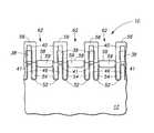
- a nitride layer 18is deposited over upper surface 13 of substrate 12 and isolations regions 14 .
- An exemplary thickness of nitride layer 18that is the height in which nitride layer 18 extends upward from upper surface 13 , ranges from about 2,000 Angstroms to about 3,000 Angstroms.
- FIGS. 5-6represent a first orientation
- FIGS. 7-8represent a second orientation that is oriented 90 degrees from the orientation of FIGS. 5-6 .
- Nitride layer 18is patterned and etched to form trenches 20 ( FIG. 8 ) that extend down to substrate 12 to expose upper surface portions 22 of substrate 12 . Trenches 20 also expose isolation region portions 24 of isolation regions 14 .
- the nitride layer 18is left patterned as nitride rows or runners 18 that extend generally in a spaced and parallel relation oriented perpendicularly to the direction of the isolation regions 14 .
- openings 31extend to upper surface portions 22 and are defined or bordered by the towers of SOG layer 30 and nitride rows 18 .
- An exemplary selective nitride etchwill over-etch nitride, for example nitride rows 18 , from 0 to about 300 angstroms and preferably stop at silicon substrate 12 .
- the exposed upper surface portions 22 of substrate 12define general surface areas of substrate 12 that will serve or function as active areas for subsequently formed devices and/or structures.
- etching and planarization processingcan be performed to elevationally lower the upper surfaces of nitride rows 18 and SOG layer 30 relative silicon substrate 12 to a pre-selected elevation or height above upper surface portions 22 .
- Such pre-selected height of nitride rows 18 and SOG layer 30facilitates the formation of a pre-selected height of subsequently formed epitaxial structures relative substrate 12 .
- Posts or pillars 38are formed extending upward from exposed upper surface portions 22 of silicon substrate 12 through cylindrical openings 32 .
- posts or pillars 38comprise epitaxial silicon grown or formed from exposed upper surfaces portions 22 of silicon substrate 12 .
- a conductivity implant(not shown) is performed to provide a conductivity dopant into upper surface portions 22 of substrate 12 to form diffusion regions or nodes 41 .
- the conductivity dopantis implanted substantially through posts 38 leaving substantially an entirety of the conductivity dopant within silicon substrate 12 .
- a portion of the conductivity dopantremains in posts 38 to leave posts 38 electrically conductive forming a portion of the diffusion regions or nodes 41 .
- Exemplary diffusion regions 41comprise source/drain regions, for example, drain regions.
- posts 38are conductively doped but do not form a portion of diffusion regions or nodes 41 , and therefore, form electrical contacts between diffusion regions or nodes 41 of subsequently formed transistors and capacitors.
- posts 38 and diffusion regions 41comprise an entirety of one of a pair of source/drain regions of a transistor with posts 38 electrically coupled to subsequently formed capacitors.
- a conductivity implant(not shown) is performed to provide a conductivity dopant substantially only into posts 38 and then posts 38 are annealed to out-diffuse conductivity dopant from posts 38 into silicon substrate 12 to form at least a portion of diffusion regions 41 .
- diffusion regions 41are not formed wherein a conductivity implant (not shown) is performed to provide a conductivity dopant substantially only into posts 38 wherein posts 38 comprise an entirety of a one of a pair of source/drain regions.
- diffusion regions 41comprise a portion of one of a pair of source/drain regions and posts 38 comprise another portion of the one of the pair of source/drain regions.
- a wet or vapor etchis performed to remove the SOG layer 30 and the TEOS spacers 34 , and preferably to remove the SOG layer 30 and the TEOS spacers 34 entirely.
- An exemplary etchincludes a selective etch to stop etching at nitride and silicon materials such as nitride liner 28 , hard mask 40 , nitride runners 18 and upper surface portions 22 of silicon substrate 12 .
- the selective etchforms openings 42 defined by nitride liner 28 , posts 38 (including hard mask 40 ), and nitride runners 18 .
- Exemplary selective etchesinclude a diluted hydrofluoric acid etch and/or a buffered oxide etch.
- a selective dry etchis performed to remove upper surface portions 22 of substrate 12 adjacent posts 38 and down to isolation regions 14 .
- the selective etchalso removes portions of isolation regions 14 and leaves portions of silicon substrate 12 remaining directly below or beneath posts 38 and referred to as silicon support structures 46 .
- Exemplary silicon support structures 46are generally annular or cylindrical in shape, similar to posts 38 which extend elevationally above silicon support structures 46 .
- the selective etchenlarges openings 42 to form openings 44 with a bottom periphery defined by silicon support structures 46 , upper surface 48 of silicon substrate 12 , and upper surface 50 of isolation regions 14 .
- the punch etchwill etch or recess the silicon substrate 12 to slightly below the upper surface 50 of isolation regions 14 leaving upper surface 48 elevationally below upper surface 50 .
- transistor channel 46(alternatively referred to as vertical channel 46 ) will depend on the selective etch processing step, for example, the length of time the selective etch is allowed to remove and etch down into silicon substrate 12 (i.e., the depth of the selective etch into substrate 12 ).
- a conductive materialis deposited over gate dielectrics 52 and will serve or function as transistor gates or word lines 54 .
- An exemplary method of forming conductive material for transistor gates 54includes depositing polysilicon material within openings 44 , removing portions of the polysilicon material by CMP processing down to nitride runners 18 , and then recessing the polysilicon material within openings 44 to below epitaxial silicon posts 38 .
- an upper surface 55 of transistor gates 54is formed about 1,000 angstroms elevationally below upper surfaces 39 of epitaxial silicon posts 38 .
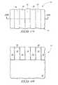
- FIGS. 49-50such illustrates a semiconductor construction 100 according to some exemplary embodiments at a processing stage subsequent to the processing stages of FIGS. 1-48 , for example, subsequent to the processing stages of FIGS. 45-48 .
- FIG. 49represents a view orientation of semiconductor construction 100 similar to the view orientation of FIG. 46 at a subsequent processing stage.
- FIG. 50represents a view orientation of semiconductor construction 100 similar to the view orientation of FIG. 48 at a subsequent processing stage. It should be understood that FIG. 50 is a view of the semiconductor construction 100 of FIG. 49 and rotated 90° from the orientation of the view for FIG. 49 .
- FIGS. 49-50illustrate exemplary transistor devices electrically coupled with exemplary charge storage devices or data storage elements, for example, capacitor devices.
- Such exemplary combinations of transistors and capacitorsare representative of memory and/or logic circuitry comprising memory cells such as DRAMs.
- An exemplary transistor deviceis referenced generally as numeral 69 and an exemplary charge storage device or data storage element, for example, a capacitor device is referenced generally as numeral 80 .
- An exemplary transistor 69comprises a gate 54 , a gate dielectric 52 and source/drain regions 41 and 59 ( FIG. 50 ).
- Exemplary transistor 69further includes a channel represented generally as the region of substrate 12 where current flow 71 is illustrated in FIG. 50 extending around gate 54 (and gate dielectric 52 ) from source/drain region 59 to source/drain region 41 .
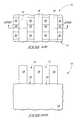
- An exemplary portion of the channelcomprises silicon support structures 46 that extend directly elevationally below source/drain regions 41 .
- Exemplary channel portions defined by silicon support structures 46are cylindrical or annular portions of silicon substrate 12 .
- Exemplary source/drain regions 41comprise drain regions.
- Exemplary source/drain regions 59comprise source regions.
- a single source/drain region 59will comprise an entirety of the source region for transistor 69 .
- a pair of source/drain regions 59 formed on opposite sides of gate 54will comprise an entirety of the source region for transistor 69 .
- activation of transistor 69establishes current flow 71 from source region 59 downward through silicon substrate 12 below and around a bottom end of gate 54 and back upward through the channel portion 46 and to drain region 41 .
- Conductive material 102is formed over and in contact with posts 38 to form an electrical contact.
- Exemplary conductive material 102is polysilicon to form polysilicon plugs or cell plugs 102 for electrical coupling transistors 69 via posts 38 to subsequently formed devices, for example, capacitors 80 .
Landscapes
- Engineering & Computer Science (AREA)
- Manufacturing & Machinery (AREA)
- Semiconductor Memories (AREA)
- Insulated Gate Type Field-Effect Transistor (AREA)
- Metal-Oxide And Bipolar Metal-Oxide Semiconductor Integrated Circuits (AREA)
Abstract
Description
Claims (10)
Priority Applications (1)
| Application Number | Priority Date | Filing Date | Title |
|---|---|---|---|
| US12/891,407US8120101B2 (en) | 2004-09-01 | 2010-09-27 | Semiconductor constructions and transistors, and methods of forming semiconductor constructions and transistors |
Applications Claiming Priority (3)
| Application Number | Priority Date | Filing Date | Title |
|---|---|---|---|
| US10/932,150US7547945B2 (en) | 2004-09-01 | 2004-09-01 | Transistor devices, transistor structures and semiconductor constructions |
| US12/070,078US7825462B2 (en) | 2004-09-01 | 2008-02-15 | Transistors |
| US12/891,407US8120101B2 (en) | 2004-09-01 | 2010-09-27 | Semiconductor constructions and transistors, and methods of forming semiconductor constructions and transistors |
Related Parent Applications (1)
| Application Number | Title | Priority Date | Filing Date |
|---|---|---|---|
| US12/070,078ContinuationUS7825462B2 (en) | 2004-09-01 | 2008-02-15 | Transistors |
Publications (2)
| Publication Number | Publication Date |
|---|---|
| US20110012182A1 US20110012182A1 (en) | 2011-01-20 |
| US8120101B2true US8120101B2 (en) | 2012-02-21 |
Family
ID=35632014
Family Applications (4)
| Application Number | Title | Priority Date | Filing Date |
|---|---|---|---|
| US10/932,150Expired - LifetimeUS7547945B2 (en) | 2004-09-01 | 2004-09-01 | Transistor devices, transistor structures and semiconductor constructions |
| US11/496,930Expired - LifetimeUS7501684B2 (en) | 2004-09-01 | 2006-07-31 | Methods of forming semiconductor constructions |
| US12/070,078Expired - LifetimeUS7825462B2 (en) | 2004-09-01 | 2008-02-15 | Transistors |
| US12/891,407Expired - LifetimeUS8120101B2 (en) | 2004-09-01 | 2010-09-27 | Semiconductor constructions and transistors, and methods of forming semiconductor constructions and transistors |
Family Applications Before (3)
| Application Number | Title | Priority Date | Filing Date |
|---|---|---|---|
| US10/932,150Expired - LifetimeUS7547945B2 (en) | 2004-09-01 | 2004-09-01 | Transistor devices, transistor structures and semiconductor constructions |
| US11/496,930Expired - LifetimeUS7501684B2 (en) | 2004-09-01 | 2006-07-31 | Methods of forming semiconductor constructions |
| US12/070,078Expired - LifetimeUS7825462B2 (en) | 2004-09-01 | 2008-02-15 | Transistors |
Country Status (8)
| Country | Link |
|---|---|
| US (4) | US7547945B2 (en) |
| EP (2) | EP1784858A2 (en) |
| JP (1) | JP2008511996A (en) |
| KR (1) | KR100918156B1 (en) |
| CN (1) | CN100583414C (en) |
| SG (1) | SG155882A1 (en) |
| TW (1) | TWI287270B (en) |
| WO (1) | WO2006028775A2 (en) |
Cited By (1)
| Publication number | Priority date | Publication date | Assignee | Title |
|---|---|---|---|---|
| US11251189B2 (en) | 2009-02-09 | 2022-02-15 | Longitude Flash Memory Solutions Ltd. | Gate fringing effect based channel formation for semiconductor device |
Families Citing this family (34)
| Publication number | Priority date | Publication date | Assignee | Title |
|---|---|---|---|---|
| US7547945B2 (en) | 2004-09-01 | 2009-06-16 | Micron Technology, Inc. | Transistor devices, transistor structures and semiconductor constructions |
| US7384849B2 (en) | 2005-03-25 | 2008-06-10 | Micron Technology, Inc. | Methods of forming recessed access devices associated with semiconductor constructions |
| US7888721B2 (en)* | 2005-07-06 | 2011-02-15 | Micron Technology, Inc. | Surround gate access transistors with grown ultra-thin bodies |
| US7282401B2 (en) | 2005-07-08 | 2007-10-16 | Micron Technology, Inc. | Method and apparatus for a self-aligned recessed access device (RAD) transistor gate |
| US7768051B2 (en)* | 2005-07-25 | 2010-08-03 | Micron Technology, Inc. | DRAM including a vertical surround gate transistor |
| US7867851B2 (en) | 2005-08-30 | 2011-01-11 | Micron Technology, Inc. | Methods of forming field effect transistors on substrates |
| US7696567B2 (en) | 2005-08-31 | 2010-04-13 | Micron Technology, Inc | Semiconductor memory device |
| US7416943B2 (en) | 2005-09-01 | 2008-08-26 | Micron Technology, Inc. | Peripheral gate stacks and recessed array gates |
| US7557032B2 (en) | 2005-09-01 | 2009-07-07 | Micron Technology, Inc. | Silicided recessed silicon |
| US7687342B2 (en) | 2005-09-01 | 2010-03-30 | Micron Technology, Inc. | Method of manufacturing a memory device |
| DE102005051417A1 (en)* | 2005-10-27 | 2007-05-03 | X-Fab Semiconductor Foundries Ag | Simulation or layout method for vertical power transistors with variable channel width and variable gate-drain capacitance |
| US7700441B2 (en) | 2006-02-02 | 2010-04-20 | Micron Technology, Inc. | Methods of forming field effect transistors, methods of forming field effect transistor gates, methods of forming integrated circuitry comprising a transistor gate array and circuitry peripheral to the gate array, and methods of forming integrated circuitry comprising a transistor gate array including first gates and second grounded isolation gates |
| US7602001B2 (en) | 2006-07-17 | 2009-10-13 | Micron Technology, Inc. | Capacitorless one transistor DRAM cell, integrated circuitry comprising an array of capacitorless one transistor DRAM cells, and method of forming lines of capacitorless one transistor DRAM cells |
| US7772632B2 (en) | 2006-08-21 | 2010-08-10 | Micron Technology, Inc. | Memory arrays and methods of fabricating memory arrays |
| US7745319B2 (en)* | 2006-08-22 | 2010-06-29 | Micron Technology, Inc. | System and method for fabricating a fin field effect transistor |
| US7589995B2 (en) | 2006-09-07 | 2009-09-15 | Micron Technology, Inc. | One-transistor memory cell with bias gate |
| US7923373B2 (en) | 2007-06-04 | 2011-04-12 | Micron Technology, Inc. | Pitch multiplication using self-assembling materials |
| US8072345B2 (en)* | 2008-02-14 | 2011-12-06 | Darren Gallo | Electronic flare system and apparatus |
| KR101145396B1 (en)* | 2008-04-04 | 2012-05-16 | 에스케이하이닉스 주식회사 | Vertical gate forming method and semiconductor device manufacturing method using same |
| KR100983693B1 (en)* | 2008-04-10 | 2010-09-24 | 주식회사 하이닉스반도체 | Method of fabricating vertical transistor in high integrated semiconductor apparatus |
| US8039399B2 (en)* | 2008-10-09 | 2011-10-18 | Micron Technology, Inc. | Methods of forming patterns utilizing lithography and spacers |
| KR101014855B1 (en)* | 2008-12-22 | 2011-02-15 | 주식회사 하이닉스반도체 | How to form a cylindrical capacitor |
| KR101061321B1 (en)* | 2009-03-02 | 2011-08-31 | 주식회사 하이닉스반도체 | Saddle pin transistor with raised landing plug contact and its formation method |
| KR101075492B1 (en)* | 2009-03-23 | 2011-10-21 | 주식회사 하이닉스반도체 | Semiconductor device with vertical transistor and method for fabricating the same |
| KR101159900B1 (en)* | 2009-04-22 | 2012-06-25 | 에스케이하이닉스 주식회사 | Semiconductor device and method of fabricating the same |
| KR101927991B1 (en)* | 2012-07-16 | 2018-12-12 | 에스케이하이닉스 주식회사 | Vertical semiconductor device, module and system having the device and method of the device |
| TWI560481B (en)* | 2012-10-29 | 2016-12-01 | Hon Hai Prec Ind Co Ltd | Photoelectric converting module |
| CN106611763B (en)* | 2015-10-21 | 2019-06-14 | 华邦电子股份有限公司 | Memory device and its manufacturing method |
| US10002962B2 (en) | 2016-04-27 | 2018-06-19 | International Business Machines Corporation | Vertical FET structure |
| US9799765B1 (en) | 2016-06-29 | 2017-10-24 | International Business Machines Corporation | Formation of a bottom source-drain for vertical field-effect transistors |
| US9847337B1 (en)* | 2016-12-27 | 2017-12-19 | Micron Technology, Inc. | Memory arrays comprising ferroelectric capacitors |
| US10553703B2 (en)* | 2017-05-19 | 2020-02-04 | Micron Technology, Inc. | Array of elevationally-extending transistors and a method used in forming an array of elevationally-extending transistors |
| CN108461496B (en)* | 2018-05-09 | 2023-09-29 | 长鑫存储技术有限公司 | Integrated circuit memory, forming method thereof and semiconductor integrated circuit device |
| KR20220169503A (en)* | 2021-06-18 | 2022-12-28 | 삼성전자주식회사 | Semiconductor devices |
Citations (218)
| Publication number | Priority date | Publication date | Assignee | Title |
|---|---|---|---|---|
| US4835741A (en) | 1986-06-02 | 1989-05-30 | Texas Instruments Incorporated | Frasable electrically programmable read only memory cell using a three dimensional trench floating gate |
| US4922460A (en) | 1987-01-26 | 1990-05-01 | Mitsubishi Denki Kabushiki Kaisha | Semiconductor memory device with folded bit line structure suitable for high density |
| US4931409A (en) | 1988-01-30 | 1990-06-05 | Kabushiki Kaisha Toshiba | Method of manufacturing semiconductor device having trench isolation |
| US4979004A (en) | 1988-01-29 | 1990-12-18 | Texas Instruments Incorporated | Floating gate memory cell and device |
| US5013680A (en) | 1990-07-18 | 1991-05-07 | Micron Technology, Inc. | Process for fabricating a DRAM array having feature widths that transcend the resolution limit of available photolithography |
| US5014110A (en) | 1988-06-03 | 1991-05-07 | Mitsubishi Denki Kabushiki Kaisha | Wiring structures for semiconductor memory device |
| US5047117A (en) | 1990-09-26 | 1991-09-10 | Micron Technology, Inc. | Method of forming a narrow self-aligned, annular opening in a masking layer |
| US5107459A (en) | 1990-04-20 | 1992-04-21 | International Business Machines Corporation | Stacked bit-line architecture for high density cross-point memory cell array |
| US5122848A (en) | 1991-04-08 | 1992-06-16 | Micron Technology, Inc. | Insulated-gate vertical field-effect transistor with high current drive and minimum overlap capacitance |
| US5160491A (en) | 1986-10-21 | 1992-11-03 | Texas Instruments Incorporated | Method of making a vertical MOS transistor |
| US5254218A (en) | 1992-04-22 | 1993-10-19 | Micron Technology, Inc. | Masking layer having narrow isolated spacings and the method for forming said masking layer and the method for forming narrow isolated trenches defined by said masking layer |
| US5281548A (en) | 1992-07-28 | 1994-01-25 | Micron Technology, Inc. | Plug-based floating gate memory |
| US5358879A (en) | 1993-04-30 | 1994-10-25 | Loral Federal Systems Company | Method of making gate overlapped lightly doped drain for buried channel devices |
| US5371024A (en) | 1988-09-30 | 1994-12-06 | Kabushiki Kaisha Toshiba | Semiconductor device and process for manufacturing the same |
| US5376575A (en) | 1991-09-26 | 1994-12-27 | Hyundai Electronics Industries, Inc. | Method of making dynamic random access memory having a vertical transistor |
| US5392237A (en) | 1992-09-25 | 1995-02-21 | Rohm Co., Ltd. | Semiconductor memory device with EEPROM in trench with polysilicon/metal contacting to source and drain in virtual ground type array |
| US5413949A (en) | 1994-04-26 | 1995-05-09 | United Microelectronics Corporation | Method of making self-aligned MOSFET |
| US5446299A (en) | 1994-04-29 | 1995-08-29 | International Business Machines Corporation | Semiconductor random access memory cell on silicon-on-insulator with dual control gates |
| US5467305A (en) | 1992-03-12 | 1995-11-14 | International Business Machines Corporation | Three-dimensional direct-write EEPROM arrays and fabrication methods |
| US5532089A (en) | 1993-12-23 | 1996-07-02 | International Business Machines Corporation | Simplified fabrication methods for rim phase-shift masks |
| US5574621A (en) | 1995-03-27 | 1996-11-12 | Motorola, Inc. | Integrated circuit capacitor having a conductive trench |
| US5573837A (en) | 1992-04-22 | 1996-11-12 | Micron Technology, Inc. | Masking layer having narrow isolated spacings and the method for forming said masking layer and the method for forming narrow isolated trenches defined by said masking layer |
| US5619057A (en) | 1994-01-19 | 1997-04-08 | Sony Corporation | Complex film overlying a substrate with defined work function |
| EP0453998B1 (en) | 1990-04-21 | 1997-07-02 | Kabushiki Kaisha Toshiba | Semiconductor memory device having a bit line constituted by a semiconductor layer |
| US5693549A (en) | 1994-09-13 | 1997-12-02 | Lg Semicon Co., Ltd. | Method of fabricating thin film transistor with supplementary gates |
| US5714786A (en) | 1996-10-31 | 1998-02-03 | Micron Technology, Inc. | Transistors having controlled conductive spacers, uses of such transistors and methods of making such transistors |
| US5714412A (en) | 1996-12-02 | 1998-02-03 | Taiwan Semiconductor Manufacturing Company, Ltd | Multi-level, split-gate, flash memory cell and method of manufacture thereof |
| US5739066A (en) | 1996-09-17 | 1998-04-14 | Micron Technology, Inc. | Semiconductor processing methods of forming a conductive gate and line |
| US5753947A (en) | 1995-01-20 | 1998-05-19 | Micron Technology, Inc. | Very high-density DRAM cell structure and method for fabricating it |
| US5792690A (en) | 1997-05-15 | 1998-08-11 | Vanguard International Semiconductor Corporation | Method of fabricating a DRAM cell with an area equal to four times the used minimum feature |
| US5792687A (en) | 1996-08-01 | 1998-08-11 | Vanguard International Semiconductor Corporation | Method for fabricating high density integrated circuits using oxide and polysilicon spacers |
| US5798544A (en) | 1994-04-22 | 1998-08-25 | Nec Corporation | Semiconductor memory device having trench isolation regions and bit lines formed thereover |
| US5817552A (en) | 1995-05-24 | 1998-10-06 | Siemens Aktiengesellschaft | Process of making a dram cell arrangement |
| US5841611A (en) | 1994-05-02 | 1998-11-24 | Matsushita Electric Industrial Co., Ltd. | Magnetoresistance effect device and magnetoresistance effect type head, memory device, and amplifying device using the same |
| US5869382A (en) | 1996-07-02 | 1999-02-09 | Sony Corporation | Structure of capacitor for dynamic random access memory and method of manufacturing thereof |
| US5869359A (en) | 1997-08-20 | 1999-02-09 | Prabhakar; Venkatraman | Process for forming silicon on insulator devices having elevated source and drain regions |
| US5909618A (en) | 1997-07-08 | 1999-06-01 | Micron Technology, Inc. | Method of making memory cell with vertical transistor and buried word and body lines |
| US5963469A (en) | 1998-02-24 | 1999-10-05 | Micron Technology, Inc. | Vertical bipolar read access for low voltage memory cell |
| US5972754A (en) | 1998-06-10 | 1999-10-26 | Mosel Vitelic, Inc. | Method for fabricating MOSFET having increased effective gate length |
| US5977579A (en) | 1998-12-03 | 1999-11-02 | Micron Technology, Inc. | Trench dram cell with vertical device and buried word lines |
| US6033963A (en) | 1999-08-30 | 2000-03-07 | Taiwan Semiconductor Manufacturing Company | Method of forming a metal gate for CMOS devices using a replacement gate process |
| US6037212A (en) | 1996-08-16 | 2000-03-14 | United Microelectronics Corp. | Method of fabricating a semiconductor memory cell having a tree-type capacitor |
| US6054355A (en) | 1997-06-30 | 2000-04-25 | Kabushiki Kaisha Toshiba | Method of manufacturing a semiconductor device which includes forming a dummy gate |
| US6059553A (en) | 1996-12-17 | 2000-05-09 | Texas Instruments Incorporated | Integrated circuit dielectrics |
| US6072209A (en) | 1997-07-08 | 2000-06-06 | Micro Technology, Inc. | Four F2 folded bit line DRAM cell structure having buried bit and word lines |
| US6090700A (en) | 1996-03-15 | 2000-07-18 | Vanguard International Semiconductor Corporation | Metallization method for forming interconnects in an integrated circuit |
| US6108191A (en) | 1996-05-21 | 2000-08-22 | Siemens Aktiengesellschaft | Multilayer capacitor with high specific capacitance and production process therefor |
| US6114735A (en) | 1999-07-02 | 2000-09-05 | Micron Technology, Inc. | Field effect transistors and method of forming field effect transistors |
| US6150687A (en) | 1997-07-08 | 2000-11-21 | Micron Technology, Inc. | Memory cell having a vertical transistor with buried source/drain and dual gates |
| US6168996B1 (en) | 1997-08-28 | 2001-01-02 | Hitachi, Ltd. | Method of fabricating semiconductor device |
| EP1067597A2 (en) | 1999-05-07 | 2001-01-10 | Chartered Semiconductor Manufacturing Pte Ltd. | Transitors with low overlap capacitance |
| US6184086B1 (en) | 1995-11-20 | 2001-02-06 | Micron Technology Inc. | Method for forming a floating gate semiconductor device having a portion within a recess |
| US6187643B1 (en) | 1999-06-29 | 2001-02-13 | Varian Semiconductor Equipment Associates, Inc. | Simplified semiconductor device manufacturing using low energy high tilt angle and high energy post-gate ion implantation (PoGI) |
| US6191470B1 (en) | 1997-07-08 | 2001-02-20 | Micron Technology, Inc. | Semiconductor-on-insulator memory cell with buried word and body lines |
| EP1089344A2 (en) | 1999-09-29 | 2001-04-04 | Kabushiki Kaisha Toshiba | Insulated gate field effect transistor and method of fabricating the same |
| US6215149B1 (en) | 1998-08-18 | 2001-04-10 | Samsung Electronics Co., Ltd. | Trenched gate semiconductor device |
| US6225669B1 (en) | 1998-09-30 | 2001-05-01 | Advanced Micro Devices, Inc. | Non-uniform gate/dielectric field effect transistor |
| US6255165B1 (en) | 1999-10-18 | 2001-07-03 | Advanced Micro Devices, Inc. | Nitride plug to reduce gate edge lifting |
| US6258650B1 (en) | 1995-09-19 | 2001-07-10 | Kabushiki Kaisha Toshiba | Method for manufacturing semiconductor memory device |
| US6259142B1 (en) | 1998-04-07 | 2001-07-10 | Advanced Micro Devices, Inc. | Multiple split gate semiconductor device and fabrication method |
| US6274497B1 (en) | 1999-11-25 | 2001-08-14 | Taiwan Semiconductor Manufacturing Co., Ltd. | Copper damascene manufacturing process |
| US6300177B1 (en) | 2001-01-25 | 2001-10-09 | Chartered Semiconductor Manufacturing Inc. | Method to form transistors with multiple threshold voltages (VT) using a combination of different work function gate materials |
| US6303518B1 (en) | 1999-09-30 | 2001-10-16 | Novellus Systems, Inc. | Methods to improve chemical vapor deposited fluorosilicate glass (FSG) film adhesion to metal barrier or etch stop/diffusion barrier layers |
| US6301726B1 (en) | 2000-11-27 | 2001-10-16 | Robert Pena | Method of installing a bathtub |
| US20010038123A1 (en) | 1999-08-11 | 2001-11-08 | Bin Yu | Transistor with dynamic source/drain extensions |
| US20010044181A1 (en) | 1996-11-06 | 2001-11-22 | Fujitsu Limited | Semiconductor device and method for fabricating the same |
| US6323528B1 (en) | 1991-03-06 | 2001-11-27 | Semiconductor Energy Laboratory Co,. Ltd. | Semiconductor device |
| US6323506B1 (en) | 1999-12-21 | 2001-11-27 | Philips Electronics North America Corporation | Self-aligned silicon carbide LMOSFET |
| US6331461B1 (en) | 1996-11-01 | 2001-12-18 | Micron Technology, Inc. | Semiconductor processing methods of forming devices on a substrate, forming device arrays on a substrate, forming conductive lines on a substrate, and forming capacitor arrays on a substrate, and integrated circuitry |
| US20010052617A1 (en) | 2000-03-01 | 2001-12-20 | Shindengen Electric Manufacturing Co., Ltd | Transistor and method of manufacturing the same |
| US6348385B1 (en) | 2000-11-30 | 2002-02-19 | Chartered Semiconductor Manufacturing Ltd. | Method for a short channel CMOS transistor with small overlay capacitance using in-situ doped spacers with a low dielectric constant |
| US20020022339A1 (en) | 2000-07-27 | 2002-02-21 | Markus Kirchhoff | Method for forming an insulator having a low dielectric constant on a semiconductor substrate |
| US6362506B1 (en) | 1998-08-26 | 2002-03-26 | Texas Instruments Incorporated | Minimization-feasible word line structure for DRAM cell |
| US6372554B1 (en) | 1998-09-04 | 2002-04-16 | Hitachi, Ltd. | Semiconductor integrated circuit device and method for production of the same |
| US6383879B1 (en) | 1999-12-03 | 2002-05-07 | Agere Systems Guardian Corp. | Semiconductor device having a metal gate with a work function compatible with a semiconductor device |
| US6383861B1 (en) | 1999-02-18 | 2002-05-07 | Micron Technology, Inc. | Method of fabricating a dual gate dielectric |
| US6399490B1 (en) | 2000-06-29 | 2002-06-04 | International Business Machines Corporation | Highly conformal titanium nitride deposition process for high aspect ratio structures |
| JP2002184958A (en) | 2000-12-14 | 2002-06-28 | Sony Corp | Semiconductor device and manufacturing method thereof |
| US6414356B1 (en) | 1998-03-30 | 2002-07-02 | Micron Technology, Inc. | Circuits and methods for dual-gated transistors |
| US6420786B1 (en) | 1996-02-02 | 2002-07-16 | Micron Technology, Inc. | Conductive spacer in a via |
| US20020127798A1 (en) | 2001-03-08 | 2002-09-12 | Kirk Prall | 2F2 memory device system and method |
| US20020127796A1 (en) | 2001-03-12 | 2002-09-12 | Franz Hofmann | Method for producing a cell of a semiconductor memory |
| US20020130378A1 (en) | 2001-03-15 | 2002-09-19 | Leonard Forbes | Technique to mitigate short channel effects with vertical gate transistor with different gate materials |
| US20020135030A1 (en) | 2001-03-22 | 2002-09-26 | Mitsubishi Denki Kabushiki Kaisha | Semiconductor device and manufacturing method thereof |
| US6459138B2 (en) | 1999-09-02 | 2002-10-01 | Micron Technology, Inc. | Capacitor structures |
| US6458925B1 (en) | 1998-08-03 | 2002-10-01 | University Of Maryland, Baltimore | Peptide antagonists of zonulin and methods for use of the same |
| US6458653B1 (en) | 2001-01-05 | 2002-10-01 | Samsung Electronics Co., Ltd. | Method for forming lower electrode of cylinder-shaped capacitor preventing twin bit failure |
| US20020153579A1 (en) | 2001-04-19 | 2002-10-24 | Nec Corporation | Semiconductor device with thin film having high permittivity and uniform thickness |
| US6476444B1 (en) | 1999-03-18 | 2002-11-05 | Hyundai Electronics Industries Co., Ltd. | Semiconductor device and method for fabricating the same |
| WO2002089182A2 (en) | 2001-04-27 | 2002-11-07 | Micron Technology, Inc. | Recessed gat dram transistor and method |
| US20020163039A1 (en) | 2001-05-04 | 2002-11-07 | Clevenger Lawrence A. | High dielectric constant materials as gate dielectrics (insulators) |
| US6495474B1 (en) | 2000-09-11 | 2002-12-17 | Agere Systems Inc. | Method of fabricating a dielectric layer |
| US20020192911A1 (en) | 2000-08-29 | 2002-12-19 | Parke Stephen A. | Damascene double gated transistors and related manufacturing methods |
| EP1271632A1 (en) | 2001-02-06 | 2003-01-02 | Matsushita Electric Industrial Co., Ltd. | Method of forming insulating film and method of producing semiconductor device |
| JP2003017585A (en) | 2001-06-29 | 2003-01-17 | Toshiba Corp | Semiconductor storage device and method of manufacturing the same |
| US20030042512A1 (en) | 2001-08-30 | 2003-03-06 | Micron Technology, Inc. | Vertical transistor and method of making |
| US6552401B1 (en) | 2000-11-27 | 2003-04-22 | Micron Technology | Use of gate electrode workfunction to improve DRAM refresh |
| US6563183B1 (en) | 2001-12-31 | 2003-05-13 | Advanced Micro Devices, Inc. | Gate array with multiple dielectric properties and method for forming same |
| US20030094651A1 (en) | 2001-11-17 | 2003-05-22 | Hynix Semiconductor Inc. | Transistor in semiconductor devices and method of manufacturing the same |
| US6586808B1 (en) | 2002-06-06 | 2003-07-01 | Advanced Micro Devices, Inc. | Semiconductor device having multi-work function gate electrode and multi-segment gate dielectric |
| US20030170955A1 (en) | 2001-07-10 | 2003-09-11 | Takahiro Kawamura | Trench-gate semiconductor device and its manufacturing method |
| US6624032B2 (en) | 1999-06-28 | 2003-09-23 | Intel Corporation | Structure and process flow for fabrication of dual gate floating body integrated MOS transistors |
| US6630720B1 (en) | 2001-12-26 | 2003-10-07 | Advanced Micro Devices, Inc. | Asymmetric semiconductor device having dual work function gate and method of fabrication |
| US6632723B2 (en) | 2001-04-26 | 2003-10-14 | Kabushiki Kaisha Toshiba | Semiconductor device |
| US6632714B2 (en) | 1999-03-08 | 2003-10-14 | Kabushiki Kaisha Toshiba | Method for manufacturing semiconductor memory |
| US6645869B1 (en) | 2002-09-26 | 2003-11-11 | Vanguard International Semiconductor Corporation | Etching back process to improve topographic planarization of a polysilicon layer |
| US6656748B2 (en) | 2002-01-31 | 2003-12-02 | Texas Instruments Incorporated | FeRAM capacitor post stack etch clean/repair |
| US20040009644A1 (en) | 2001-05-30 | 2004-01-15 | Toshiharu Suzuki | Method for manufacturing channel gate type field effect transistor |
| US20040018679A1 (en) | 2001-03-03 | 2004-01-29 | Yu Young Sub | Storage electrode of a semiconductor memory device and method for fabricating the same |
| TW574746B (en) | 2002-12-19 | 2004-02-01 | Taiwan Semiconductor Mfg | Method for manufacturing MOSFET with recessed channel |
| US20040034587A1 (en) | 2002-08-19 | 2004-02-19 | Amberson Matthew Gilbert | System and method for calculating intra-period volatility |
| US6696746B1 (en) | 1998-04-29 | 2004-02-24 | Micron Technology, Inc. | Buried conductors |
| US20040061148A1 (en) | 2002-03-11 | 2004-04-01 | Monolithic System Technology, Inc. | One-transistor floating-body DRAM cell in bulk CMOS process with electrically isolated charge storage region |
| US6720232B1 (en) | 2003-04-10 | 2004-04-13 | Taiwan Semiconductor Manufacturing Company | Method of fabricating an embedded DRAM for metal-insulator-metal (MIM) capacitor structure |
| US20040070028A1 (en) | 2002-10-15 | 2004-04-15 | Semiconductor Components Industries, Llc | Method of forming a low resistance semiconductor device and structure therefor |
| US6727137B2 (en) | 1997-08-22 | 2004-04-27 | Micron Technology, Inc. | Processing methods of forming integrated circuitry memory devices, methods of forming DRAM arrays, and related semiconductor masks |
| US20040125636A1 (en) | 2001-03-14 | 2004-07-01 | Wlodek Kurjanowicz | Interleaved wordline architecture |
| US6767789B1 (en) | 1998-06-26 | 2004-07-27 | International Business Machines Corporation | Method for interconnection between transfer devices and storage capacitors in memory cells and device formed thereby |
| US20040150070A1 (en) | 2003-02-03 | 2004-08-05 | Nec Electronics Corporation | Semiconductor device and method for manufacturing the same |
| US6784112B2 (en) | 2001-04-05 | 2004-08-31 | Matsushita Electric Industrial Co., Ltd. | Method for surface treatment of silicon based substrate |
| US20040184298A1 (en) | 2003-03-17 | 2004-09-23 | Hiroyuki Takahashi | Semiconductor memory device |
| US20040188738A1 (en) | 2002-03-06 | 2004-09-30 | Micron Technology, Inc. | Nanotube semiconductor devices and methods for making the same |
| US20040197995A1 (en) | 2003-04-01 | 2004-10-07 | Lee Yong-Kyu | Method of manufacturing twin-ONO-type SONOS memory using reverse self-alignment process |
| US20040224476A1 (en) | 2000-01-25 | 2004-11-11 | Satoru Yamada | Semiconductor integrated circuit device |
| US20040222458A1 (en) | 2003-05-06 | 2004-11-11 | Mosel Vitelic, Inc. | Termination structure for trench DMOS device and method of making the same |
| US6818947B2 (en) | 2002-09-19 | 2004-11-16 | Fairchild Semiconductor Corporation | Buried gate-field termination structure |
| US6818515B1 (en) | 2003-06-23 | 2004-11-16 | Promos Technologies Inc. | Method for fabricating semiconductor device with loop line pattern structure |
| US20040266081A1 (en) | 2003-06-25 | 2004-12-30 | Chang-Woo Oh | Methods of forming field effect transistors including raised source/drain regions |
| US6844591B1 (en) | 2003-09-17 | 2005-01-18 | Micron Technology, Inc. | Method of forming DRAM access transistors |
| US20050017240A1 (en) | 2003-07-22 | 2005-01-27 | Pierre Fazan | Integrated circuit device, and method of fabricating same |
| US6849496B2 (en) | 2000-12-06 | 2005-02-01 | Infineon Technologies Ag | DRAM with vertical transistor and trench capacitor memory cells and method of fabrication |
| US20050042833A1 (en) | 2003-08-20 | 2005-02-24 | Jong-Chul Park | Method of manufacturing integrated circuit device including recessed channel transistor |
| US20050063224A1 (en) | 2003-09-24 | 2005-03-24 | Pierre Fazan | Low power programming technique for a floating body memory transistor, memory cell, and memory array |
| US6888770B2 (en) | 2003-05-09 | 2005-05-03 | Kabushiki Kaisha Toshiba | Semiconductor memory device |
| US6888198B1 (en) | 2001-06-04 | 2005-05-03 | Advanced Micro Devices, Inc. | Straddled gate FDSOI device |
| US20050104156A1 (en) | 2003-11-13 | 2005-05-19 | Texas Instruments Incorporated | Forming a semiconductor structure in manufacturing a semiconductor device using one or more epitaxial growth processes |
| US20050106838A1 (en) | 2003-11-17 | 2005-05-19 | Hoon Lim | Semiconductor devices with a source/drain formed on a recessed portion of an isolation layer and methods of fabricating the same |
| US6897109B2 (en) | 2001-09-11 | 2005-05-24 | Samsung Electronics Co., Ltd. | Methods of manufacturing integrated circuit devices having contact holes using multiple insulating layers |
| US20050124130A1 (en) | 2003-04-30 | 2005-06-09 | Leo Mathew | Semiconductor fabrication process with asymmetrical conductive spacers |
| US6916711B2 (en) | 2001-08-02 | 2005-07-12 | Samsung Electronics Co., Ltd. | EEPROM memory cell and method of forming the same |
| US20050158949A1 (en) | 2003-09-04 | 2005-07-21 | Manning Homer M. | Semiconductor devices |
| US20050167751A1 (en) | 2004-02-02 | 2005-08-04 | Kabushiki Kaisha Toshiba | Semiconductor memory device for storing data as state of majority carriers accumulated in channel body and method of manufacturing the same |
| US6930640B2 (en) | 2003-03-28 | 2005-08-16 | Gemtek Technology Co., Ltd. | Dual frequency band inverted-F antenna |
| US6969662B2 (en) | 2001-06-18 | 2005-11-29 | Pierre Fazan | Semiconductor device |
| US20050287780A1 (en) | 2003-09-04 | 2005-12-29 | Micron Technology, Inc. | Semiconductor constructions |
| US20060046424A1 (en) | 2004-08-24 | 2006-03-02 | Chance Randal W | Methods of forming semiconductor constructions |
| US20060046407A1 (en) | 2004-09-01 | 2006-03-02 | Werner Juengling | DRAM cells with vertical transistors |
| US7027334B2 (en) | 2003-05-09 | 2006-04-11 | Kabushiki Kaisha Toshiba | Semiconductor memory device |
| US7030436B2 (en) | 2002-12-04 | 2006-04-18 | Micron Technology, Inc. | Embedded DRAM gain memory cell having MOS transistor body provided with a bi-polar transistor charge injecting means |
| US20060083058A1 (en) | 2004-10-04 | 2006-04-20 | Kabushiki Kaisha Toshiba | Semiconductor memory and FBC memory cell driving method |
| US7042009B2 (en) | 2004-06-30 | 2006-05-09 | Intel Corporation | High mobility tri-gate devices and methods of fabrication |
| US7064365B2 (en) | 2002-11-11 | 2006-06-20 | Samsung Electronics Co., Ltd. | Ferroelectric capacitors including a seed conductive film |
| US7071043B2 (en) | 2002-08-15 | 2006-07-04 | Micron Technology, Inc. | Methods of forming a field effect transistor having source/drain material over insulative material |
| US20060167741A1 (en) | 2005-01-25 | 2006-07-27 | Cisco Technology, Inc. | System and method for designing a supply chain |
| US20060194410A1 (en) | 2005-02-28 | 2006-08-31 | Hiroyuki Sugaya | Semiconductor device with cavity and method of manufacture thereof |
| US20060216922A1 (en) | 2005-03-28 | 2006-09-28 | Tran Luan C | Integrated circuit fabrication |
| US7122449B2 (en)* | 2002-06-10 | 2006-10-17 | Amberwave Systems Corporation | Methods of fabricating semiconductor structures having epitaxially grown source and drain elements |
| US7125774B2 (en) | 2003-09-09 | 2006-10-24 | Samsung Electronics Co., Ltd. | Method of manufacturing transistor having recessed channel |
| US7135371B2 (en) | 2002-12-31 | 2006-11-14 | Dongbu Electronics, Co., Ltd. | Methods of fabricating semiconductor devices |
| US20060264001A1 (en) | 2004-08-31 | 2006-11-23 | Luan Tran | Structures with increased photo-alignment margins |
| US7148527B2 (en) | 2002-12-18 | 2006-12-12 | Samsung Electronics Co., Ltd. | Semiconductor devices with enlarged recessed gate electrodes |
| US20070001222A1 (en) | 2005-06-30 | 2007-01-04 | Freescale Semiconductor, Inc. | Single transistor memory cell with reduced recombination rates |
| US7160788B2 (en) | 2004-08-23 | 2007-01-09 | Micron Technology, Inc. | Methods of forming integrated circuits |
| US7179706B2 (en) | 2003-08-29 | 2007-02-20 | Micron Technology, Inc. | Permeable capacitor electrode |
| US20070045712A1 (en) | 2005-09-01 | 2007-03-01 | Haller Gordon A | Memory cell layout and process flow |
| US20070048941A1 (en) | 2005-09-01 | 2007-03-01 | Micron Technology, Inc. | Transistor gate forming methods and transistor structures |
| US20070048942A1 (en) | 2005-08-30 | 2007-03-01 | Micron Technology, Inc. | Methods of forming field effect transistors on substrates |
| US20070061997A1 (en) | 2005-03-25 | 2007-03-22 | Toshiba Tec Kabushiki Kaisha | Electric vacuum cleaner |
| US7199005B2 (en) | 2005-08-02 | 2007-04-03 | Micron Technology, Inc. | Methods of forming pluralities of capacitors |
| US7202127B2 (en) | 2004-08-27 | 2007-04-10 | Micron Technology, Inc. | Methods of forming a plurality of capacitors |
| US20070096204A1 (en) | 2005-10-28 | 2007-05-03 | Elpida Memory, Inc. | Method for manufacturing semiconductor device |
| US7214621B2 (en) | 2005-05-18 | 2007-05-08 | Micron Technology, Inc. | Methods of forming devices associated with semiconductor constructions |
| US20070117310A1 (en) | 2005-03-15 | 2007-05-24 | Micron Technology, Inc. | Multiple deposition for integration of spacers in pitch multiplication process |
| US20070128856A1 (en) | 2005-03-15 | 2007-06-07 | Micron Technology, Inc. | Pitch reduced patterns relative to photolithography features |
| US20070148984A1 (en) | 2004-09-02 | 2007-06-28 | Micron Technology, Inc. | Method for integrated circuit fabrication using pitch multiplication |
| US20070158719A1 (en) | 2006-01-11 | 2007-07-12 | Promos Technologies Inc. | Dynamic random access memory structure and method for preparing the same |
| US7244659B2 (en) | 2005-03-10 | 2007-07-17 | Micron Technology, Inc. | Integrated circuits and methods of forming a field effect transistor |
| US7250650B2 (en) | 2002-11-21 | 2007-07-31 | Infineon Technologies Ag | Field-effect transistor structure and associated semiconductor memory cell |
| US20070178641A1 (en) | 2006-02-02 | 2007-08-02 | Micron Technology, Inc. | Methods of forming field effect transistors, methods of forming field effect transistor gates, methods of forming integrated circuitry comprising a transistor gate array and circuitry peripheral to the gate array, and methods of forming integrated circuitry comprising a transistor gate array including first gates and second grounded isolation gates |
| US7262089B2 (en) | 2004-03-11 | 2007-08-28 | Micron Technology, Inc. | Methods of forming semiconductor structures |
| US20070238308A1 (en) | 2006-04-07 | 2007-10-11 | Ardavan Niroomand | Simplified pitch doubling process flow |
| US7282401B2 (en) | 2005-07-08 | 2007-10-16 | Micron Technology, Inc. | Method and apparatus for a self-aligned recessed access device (RAD) transistor gate |
| US7285812B2 (en) | 2004-09-02 | 2007-10-23 | Micron Technology, Inc. | Vertical transistors |
| US20070261016A1 (en) | 2006-04-24 | 2007-11-08 | Sandhu Gurtej S | Masking techniques and templates for dense semiconductor fabrication |
| US20080012056A1 (en) | 2006-07-17 | 2008-01-17 | Micron Technology, Inc. | Capacitorless one transistor dram cell, integrated circuitry comprising an array of capacitorless one transistor dram cells, and method of forming lines of capacitorless one transistor dram cells |
| US20080042179A1 (en) | 2006-08-21 | 2008-02-21 | Micron Technology, Inc. | Memory arrays and methods of fabricating memory arrays |
| US20080061346A1 (en) | 2006-09-07 | 2008-03-13 | Micron Technology, Inc. | One-transistor memory cell with bias gate |
| US7349232B2 (en) | 2006-03-15 | 2008-03-25 | Micron Technology, Inc. | 6F2 DRAM cell design with 3F-pitch folded digitline sense amplifier |
| US7351666B2 (en) | 2006-03-17 | 2008-04-01 | International Business Machines Corporation | Layout and process to contact sub-lithographic structures |
| US7384849B2 (en) | 2005-03-25 | 2008-06-10 | Micron Technology, Inc. | Methods of forming recessed access devices associated with semiconductor constructions |
| US7393789B2 (en) | 2005-09-01 | 2008-07-01 | Micron Technology, Inc. | Protective coating for planarization |
| US7396781B2 (en) | 2005-06-09 | 2008-07-08 | Micron Technology, Inc. | Method and apparatus for adjusting feature size and position |
| US7413981B2 (en) | 2005-07-29 | 2008-08-19 | Micron Technology, Inc. | Pitch doubled circuit layout |
| US7429536B2 (en) | 2005-05-23 | 2008-09-30 | Micron Technology, Inc. | Methods for forming arrays of small, closely spaced features |
| US7435536B2 (en) | 2004-09-02 | 2008-10-14 | Micron Technology, Inc. | Method to align mask patterns |
| US20080299774A1 (en) | 2007-06-04 | 2008-12-04 | Micron Technology, Inc. | Pitch multiplication using self-assembling materials |
| US20090035665A1 (en) | 2007-07-31 | 2009-02-05 | Micron Technology, Inc. | Process of semiconductor fabrication with mask overlay on pitch multiplied features and associated structures |
| US7488685B2 (en) | 2006-04-25 | 2009-02-10 | Micron Technology, Inc. | Process for improving critical dimension uniformity of integrated circuit arrays |
| US7495946B2 (en) | 2006-03-02 | 2009-02-24 | Infineon Technologies Ag | Phase change memory fabricated using self-aligned processing |
| US7494870B2 (en) | 2007-01-12 | 2009-02-24 | Sandisk Corporation | Methods of forming NAND memory with virtual channel |
| US7495294B2 (en) | 2005-12-21 | 2009-02-24 | Sandisk Corporation | Flash devices with shared word lines |
| US7504686B2 (en) | 2003-06-20 | 2009-03-17 | Sandisk Corporation | Self-aligned non-volatile memory cell |
| US7528440B2 (en) | 2003-03-04 | 2009-05-05 | Micron Technology, Inc. | Vertical gain cell |
| US7535745B2 (en) | 2005-06-20 | 2009-05-19 | Kabushiki Kaisha Toshiba | Ferroelectric memory device and method of manufacturing the same |
| US7547945B2 (en) | 2004-09-01 | 2009-06-16 | Micron Technology, Inc. | Transistor devices, transistor structures and semiconductor constructions |
| US7560390B2 (en) | 2005-06-02 | 2009-07-14 | Micron Technology, Inc. | Multiple spacer steps for pitch multiplication |
| US7564087B2 (en) | 2002-08-29 | 2009-07-21 | Micron Technology, Inc. | Merged MOS-bipolar capacitor memory cell |
| US7567452B2 (en) | 2005-12-15 | 2009-07-28 | Samsung Electronics Co., Ltd. | Multi-level dynamic memory device having open bit line structure and method of driving the same |
| EP1696477B1 (en) | 2005-02-24 | 2009-09-02 | Infineon Technologies AG | Process of fabrication of sub-lithographic structures |
| US7608503B2 (en) | 2004-11-22 | 2009-10-27 | Macronix International Co., Ltd. | Side wall active pin memory and manufacturing method |
| US7619311B2 (en) | 2007-02-02 | 2009-11-17 | Macronix International Co., Ltd. | Memory cell device with coplanar electrode surface and method |
| US7684245B2 (en) | 2007-10-30 | 2010-03-23 | Atmel Corporation | Non-volatile memory array architecture with joined word lines |
| EP1125167B1 (en) | 1998-10-01 | 2010-05-12 | Micron Technology, Inc. | Methods of reducing proximity effects in lithographic processes |
| US7732275B2 (en) | 2007-03-29 | 2010-06-08 | Sandisk Corporation | Methods of forming NAND flash memory with fixed charge |
| US7736980B2 (en) | 2006-03-02 | 2010-06-15 | Micron Technology, Inc. | Vertical gated access transistor |
| US7755132B2 (en) | 2006-08-16 | 2010-07-13 | Sandisk Corporation | Nonvolatile memories with shaped floating gates |
| US7759193B2 (en) | 2008-07-09 | 2010-07-20 | Micron Technology, Inc. | Methods of forming a plurality of capacitors |
| EP1003219B1 (en) | 1998-11-19 | 2011-12-28 | Qimonda AG | DRAM with stacked capacitor and buried word line |
Family Cites Families (40)
| Publication number | Priority date | Publication date | Assignee | Title |
|---|---|---|---|---|
| JPS5681974A (en)* | 1979-12-07 | 1981-07-04 | Toshiba Corp | Manufacture of mos type semiconductor device |
| KR920010461B1 (en) | 1983-09-28 | 1992-11-28 | 가부시끼가이샤 히다찌세이사꾸쇼 | Semiconductor Memory and Manufacturing Method |
| US5108938A (en)* | 1989-03-21 | 1992-04-28 | Grumman Aerospace Corporation | Method of making a trench gate complimentary metal oxide semiconductor transistor |
| US5021355A (en)* | 1989-05-22 | 1991-06-04 | International Business Machines Corporation | Method of fabricating cross-point lightly-doped drain-source trench transistor |
| JPH03219677A (en)* | 1990-01-24 | 1991-09-27 | Fujitsu Ltd | semiconductor equipment |
| KR930006930B1 (en) | 1990-04-19 | 1993-07-24 | 태흥산업 주식회사 | Improved manufacturing method of tris azo direct dye |
| US5244824A (en)* | 1990-09-05 | 1993-09-14 | Motorola, Inc. | Trench capacitor and transistor structure and method for making the same |
| JP2748072B2 (en)* | 1992-07-03 | 1998-05-06 | 三菱電機株式会社 | Semiconductor device and manufacturing method thereof |
| JP3311070B2 (en) | 1993-03-15 | 2002-08-05 | 株式会社東芝 | Semiconductor device |
| KR0141218B1 (en)* | 1993-11-24 | 1998-07-15 | 윤종용 | Fabrication method of semkonductor device |
| US5514604A (en)* | 1993-12-08 | 1996-05-07 | General Electric Company | Vertical channel silicon carbide metal-oxide-semiconductor field effect transistor with self-aligned gate for microwave and power applications, and method of making |
| ATE274585T1 (en)* | 1993-12-27 | 2004-09-15 | Kirin Brewery | DNA CHAIN FOR SYNTHESIS OF XANTHOPHYLL AND PROCESS FOR PRODUCING XANTHOPHYLL |
| DE19524092C2 (en)* | 1995-07-01 | 1997-08-07 | Hewlett Packard Gmbh | Method and device for compressing and displaying digital data, in particular the heart rate of cardiotocographs |
| DE19620625C1 (en) | 1996-05-22 | 1997-10-23 | Siemens Ag | High packing density DRAM cell array |
| TW304290B (en)* | 1996-08-16 | 1997-05-01 | United Microelectronics Corp | The manufacturing method for semiconductor memory device with capacitor |
| JP4053647B2 (en)* | 1997-02-27 | 2008-02-27 | 株式会社東芝 | Semiconductor memory device and manufacturing method thereof |
| US6337497B1 (en)* | 1997-05-16 | 2002-01-08 | International Business Machines Corporation | Common source transistor capacitor stack |
| DE19801095B4 (en)* | 1998-01-14 | 2007-12-13 | Infineon Technologies Ag | Power MOSFET |
| US6188996B1 (en)* | 1998-05-22 | 2001-02-13 | Pitney Bowes Inc. | System for metering permit mail |
| DE19845003C1 (en)* | 1998-09-30 | 2000-02-10 | Siemens Ag | Vertical MOS transistor in semiconductor substrate |
| US6114205A (en)* | 1998-10-30 | 2000-09-05 | Sony Corporation | Epitaxial channel vertical MOS transistor |
| US6180494B1 (en)* | 1999-03-11 | 2001-01-30 | Micron Technology, Inc. | Integrated circuitry, methods of fabricating integrated circuitry, methods of forming local interconnects, and methods of forming conductive lines |
| DE19928781C1 (en) | 1999-06-23 | 2000-07-06 | Siemens Ag | DRAM cell array has deep word line trenches for increasing transistor channel length and has no fixed potential word lines separating adjacent memory cells |
| DE19943760C1 (en)* | 1999-09-13 | 2001-02-01 | Infineon Technologies Ag | DRAM cell arrangement comprises a substrate with a recess containing a storage node of a capacitor |
| DE10038728A1 (en)* | 2000-07-31 | 2002-02-21 | Infineon Technologies Ag | Semiconductor memory cell arrangement and method for the production thereof |
| US6391720B1 (en) | 2000-09-27 | 2002-05-21 | Chartered Semiconductor Manufacturing Ltd. | Process flow for a performance enhanced MOSFET with self-aligned, recessed channel |
| US6340614B1 (en) | 2000-10-03 | 2002-01-22 | Vanguard International Semiconductor Corporation | Method of forming a DRAM cell |
| US6570207B2 (en)* | 2000-12-13 | 2003-05-27 | International Business Machines Corporation | Structure and method for creating vertical capacitor and anti-fuse in DRAM process employing vertical array device cell complex |
| US6864536B2 (en)* | 2000-12-20 | 2005-03-08 | Winbond Electronics Corporation | Electrostatic discharge protection circuit |
| US6531727B2 (en)* | 2001-02-09 | 2003-03-11 | Micron Technology, Inc. | Open bit line DRAM with ultra thin body transistors |
| US6624486B2 (en)* | 2001-05-23 | 2003-09-23 | International Business Machines Corporation | Method for low topography semiconductor device formation |
| DE10125967C1 (en)* | 2001-05-29 | 2002-07-11 | Infineon Technologies Ag | DRAM cell arrangement used for a semiconductor storage device comprises a matrix arrangement of storage cells stacked over each other as layers, and a capacitor connected to the MOS transistor |
| DE10139827A1 (en)* | 2001-08-14 | 2003-03-13 | Infineon Technologies Ag | Memory cell with trench capacitor and vertical selection transistor and an annular contact area formed between them |
| US6858500B2 (en)* | 2002-01-16 | 2005-02-22 | Fuji Electric Co., Ltd. | Semiconductor device and its manufacturing method |
| DE10208249B4 (en)* | 2002-02-26 | 2006-09-14 | Infineon Technologies Ag | Semiconductor memory with vertical selection transistor |
| US6756625B2 (en) | 2002-06-21 | 2004-06-29 | Micron Technology, Inc. | Memory cell and method for forming the same |
| US6853252B2 (en) | 2002-10-04 | 2005-02-08 | Intersil Corporation | Phase-lock loop having programmable bandwidth |
| FR2853319B1 (en)* | 2003-04-03 | 2005-05-06 | Rhodia Chimie Sa | RETICULABLE COMPOSITION FOR BATTERY ELECTROLYTE |
| US7468311B2 (en)* | 2003-09-30 | 2008-12-23 | Tokyo Electron Limited | Deposition of silicon-containing films from hexachlorodisilane |
| US7696567B2 (en)* | 2005-08-31 | 2010-04-13 | Micron Technology, Inc | Semiconductor memory device |
- 2004
- 2004-09-01USUS10/932,150patent/US7547945B2/ennot_activeExpired - Lifetime
- 2005
- 2005-08-29JPJP2007530233Apatent/JP2008511996A/enactivePending
- 2005-08-29EPEP05792363Apatent/EP1784858A2/ennot_activeWithdrawn
- 2005-08-29KRKR1020077004257Apatent/KR100918156B1/ennot_activeExpired - Lifetime
- 2005-08-29EPEP10011474Apatent/EP2267769A3/ennot_activeWithdrawn
- 2005-08-29WOPCT/US2005/030668patent/WO2006028775A2/enactiveSearch and Examination
- 2005-08-29CNCN200580038056Apatent/CN100583414C/ennot_activeExpired - Lifetime
- 2005-08-29SGSG200905780-3Apatent/SG155882A1/enunknown
- 2005-09-02TWTW094130193Apatent/TWI287270B/enactive
- 2006
- 2006-07-31USUS11/496,930patent/US7501684B2/ennot_activeExpired - Lifetime
- 2008
- 2008-02-15USUS12/070,078patent/US7825462B2/ennot_activeExpired - Lifetime
- 2010
- 2010-09-27USUS12/891,407patent/US8120101B2/ennot_activeExpired - Lifetime
Patent Citations (259)
| Publication number | Priority date | Publication date | Assignee | Title |
|---|---|---|---|---|
| US4835741A (en) | 1986-06-02 | 1989-05-30 | Texas Instruments Incorporated | Frasable electrically programmable read only memory cell using a three dimensional trench floating gate |
| US5160491A (en) | 1986-10-21 | 1992-11-03 | Texas Instruments Incorporated | Method of making a vertical MOS transistor |
| US4922460A (en) | 1987-01-26 | 1990-05-01 | Mitsubishi Denki Kabushiki Kaisha | Semiconductor memory device with folded bit line structure suitable for high density |
| US4979004A (en) | 1988-01-29 | 1990-12-18 | Texas Instruments Incorporated | Floating gate memory cell and device |
| US4931409A (en) | 1988-01-30 | 1990-06-05 | Kabushiki Kaisha Toshiba | Method of manufacturing semiconductor device having trench isolation |
| US5014110A (en) | 1988-06-03 | 1991-05-07 | Mitsubishi Denki Kabushiki Kaisha | Wiring structures for semiconductor memory device |
| US5371024A (en) | 1988-09-30 | 1994-12-06 | Kabushiki Kaisha Toshiba | Semiconductor device and process for manufacturing the same |
| US5107459A (en) | 1990-04-20 | 1992-04-21 | International Business Machines Corporation | Stacked bit-line architecture for high density cross-point memory cell array |
| EP0453998B1 (en) | 1990-04-21 | 1997-07-02 | Kabushiki Kaisha Toshiba | Semiconductor memory device having a bit line constituted by a semiconductor layer |
| US5013680A (en) | 1990-07-18 | 1991-05-07 | Micron Technology, Inc. | Process for fabricating a DRAM array having feature widths that transcend the resolution limit of available photolithography |
| US5047117A (en) | 1990-09-26 | 1991-09-10 | Micron Technology, Inc. | Method of forming a narrow self-aligned, annular opening in a masking layer |
| US6323528B1 (en) | 1991-03-06 | 2001-11-27 | Semiconductor Energy Laboratory Co,. Ltd. | Semiconductor device |
| US6822261B2 (en) | 1991-03-06 | 2004-11-23 | Semiconductor Energy Laboratory Co., Ltd. | Semiconductor device and method for forming the same |
| US5122848A (en) | 1991-04-08 | 1992-06-16 | Micron Technology, Inc. | Insulated-gate vertical field-effect transistor with high current drive and minimum overlap capacitance |
| US5376575A (en) | 1991-09-26 | 1994-12-27 | Hyundai Electronics Industries, Inc. | Method of making dynamic random access memory having a vertical transistor |
| US5504357A (en) | 1991-09-26 | 1996-04-02 | Hyundai Electronics Industries, Co., Ltd. | Dynamic random access memory having a vertical transistor |
| US5467305A (en) | 1992-03-12 | 1995-11-14 | International Business Machines Corporation | Three-dimensional direct-write EEPROM arrays and fabrication methods |
| US5254218A (en) | 1992-04-22 | 1993-10-19 | Micron Technology, Inc. | Masking layer having narrow isolated spacings and the method for forming said masking layer and the method for forming narrow isolated trenches defined by said masking layer |
| US5573837A (en) | 1992-04-22 | 1996-11-12 | Micron Technology, Inc. | Masking layer having narrow isolated spacings and the method for forming said masking layer and the method for forming narrow isolated trenches defined by said masking layer |
| US5281548A (en) | 1992-07-28 | 1994-01-25 | Micron Technology, Inc. | Plug-based floating gate memory |
| US5392237A (en) | 1992-09-25 | 1995-02-21 | Rohm Co., Ltd. | Semiconductor memory device with EEPROM in trench with polysilicon/metal contacting to source and drain in virtual ground type array |
| US5472893A (en) | 1992-09-25 | 1995-12-05 | Rohm Co., Ltd. | Method of making a floating gate memory device |
| US5358879A (en) | 1993-04-30 | 1994-10-25 | Loral Federal Systems Company | Method of making gate overlapped lightly doped drain for buried channel devices |
| US5532089A (en) | 1993-12-23 | 1996-07-02 | International Business Machines Corporation | Simplified fabrication methods for rim phase-shift masks |
| US5619057A (en) | 1994-01-19 | 1997-04-08 | Sony Corporation | Complex film overlying a substrate with defined work function |
| US5798544A (en) | 1994-04-22 | 1998-08-25 | Nec Corporation | Semiconductor memory device having trench isolation regions and bit lines formed thereover |
| US5512770A (en) | 1994-04-26 | 1996-04-30 | United Microelectronics Corporation | MOSFET device structure three spaced-apart deep boron implanted channel regions aligned with gate electrode of NMOSFET device |
| US5413949A (en) | 1994-04-26 | 1995-05-09 | United Microelectronics Corporation | Method of making self-aligned MOSFET |
| US5446299A (en) | 1994-04-29 | 1995-08-29 | International Business Machines Corporation | Semiconductor random access memory cell on silicon-on-insulator with dual control gates |
| US5841611A (en) | 1994-05-02 | 1998-11-24 | Matsushita Electric Industrial Co., Ltd. | Magnetoresistance effect device and magnetoresistance effect type head, memory device, and amplifying device using the same |
| US5693549A (en) | 1994-09-13 | 1997-12-02 | Lg Semicon Co., Ltd. | Method of fabricating thin film transistor with supplementary gates |
| US6096596A (en) | 1995-01-20 | 2000-08-01 | Micron Technology Inc. | Very high-density DRAM cell structure and method for fabricating it |
| US5753947A (en) | 1995-01-20 | 1998-05-19 | Micron Technology, Inc. | Very high-density DRAM cell structure and method for fabricating it |
| US5574621A (en) | 1995-03-27 | 1996-11-12 | Motorola, Inc. | Integrated circuit capacitor having a conductive trench |
| US5817552A (en) | 1995-05-24 | 1998-10-06 | Siemens Aktiengesellschaft | Process of making a dram cell arrangement |
| US6258650B1 (en) | 1995-09-19 | 2001-07-10 | Kabushiki Kaisha Toshiba | Method for manufacturing semiconductor memory device |
| US6184086B1 (en) | 1995-11-20 | 2001-02-06 | Micron Technology Inc. | Method for forming a floating gate semiconductor device having a portion within a recess |
| US6420786B1 (en) | 1996-02-02 | 2002-07-16 | Micron Technology, Inc. | Conductive spacer in a via |
| US6090700A (en) | 1996-03-15 | 2000-07-18 | Vanguard International Semiconductor Corporation | Metallization method for forming interconnects in an integrated circuit |
| US6108191A (en) | 1996-05-21 | 2000-08-22 | Siemens Aktiengesellschaft | Multilayer capacitor with high specific capacitance and production process therefor |
| US5869382A (en) | 1996-07-02 | 1999-02-09 | Sony Corporation | Structure of capacitor for dynamic random access memory and method of manufacturing thereof |
| US5792687A (en) | 1996-08-01 | 1998-08-11 | Vanguard International Semiconductor Corporation | Method for fabricating high density integrated circuits using oxide and polysilicon spacers |
| US6037212A (en) | 1996-08-16 | 2000-03-14 | United Microelectronics Corp. | Method of fabricating a semiconductor memory cell having a tree-type capacitor |
| US5739066A (en) | 1996-09-17 | 1998-04-14 | Micron Technology, Inc. | Semiconductor processing methods of forming a conductive gate and line |
| US6005273A (en) | 1996-10-31 | 1999-12-21 | Micron Technology, Inc. | Transistors having controlled conductive spacers, uses of such transistors and methods of making such transistors |
| US7005710B1 (en) | 1996-10-31 | 2006-02-28 | Micron Technology, Inc. | Transistors having controlled conductive spacers, uses of such transistors and methods of making such transistors |
| US6090693A (en) | 1996-10-31 | 2000-07-18 | Micron Technology, Inc. | Transistors having controlled conductive spacers, uses of such transistors and methods of making such transistors |
| US5714786A (en) | 1996-10-31 | 1998-02-03 | Micron Technology, Inc. | Transistors having controlled conductive spacers, uses of such transistors and methods of making such transistors |
| US6331461B1 (en) | 1996-11-01 | 2001-12-18 | Micron Technology, Inc. | Semiconductor processing methods of forming devices on a substrate, forming device arrays on a substrate, forming conductive lines on a substrate, and forming capacitor arrays on a substrate, and integrated circuitry |
| US20010044181A1 (en) | 1996-11-06 | 2001-11-22 | Fujitsu Limited | Semiconductor device and method for fabricating the same |
| US5714412A (en) | 1996-12-02 | 1998-02-03 | Taiwan Semiconductor Manufacturing Company, Ltd | Multi-level, split-gate, flash memory cell and method of manufacture thereof |
| US6059553A (en) | 1996-12-17 | 2000-05-09 | Texas Instruments Incorporated | Integrated circuit dielectrics |
| US5792690A (en) | 1997-05-15 | 1998-08-11 | Vanguard International Semiconductor Corporation | Method of fabricating a DRAM cell with an area equal to four times the used minimum feature |
| US6054355A (en) | 1997-06-30 | 2000-04-25 | Kabushiki Kaisha Toshiba | Method of manufacturing a semiconductor device which includes forming a dummy gate |
| US5909618A (en) | 1997-07-08 | 1999-06-01 | Micron Technology, Inc. | Method of making memory cell with vertical transistor and buried word and body lines |
| US6150687A (en) | 1997-07-08 | 2000-11-21 | Micron Technology, Inc. | Memory cell having a vertical transistor with buried source/drain and dual gates |
| US6072209A (en) | 1997-07-08 | 2000-06-06 | Micro Technology, Inc. | Four F2 folded bit line DRAM cell structure having buried bit and word lines |
| US6818937B2 (en) | 1997-07-08 | 2004-11-16 | Micron Technology, Inc. | Memory cell having a vertical transistor with buried source/drain and dual gates |
| US6191470B1 (en) | 1997-07-08 | 2001-02-20 | Micron Technology, Inc. | Semiconductor-on-insulator memory cell with buried word and body lines |
| US5869359A (en) | 1997-08-20 | 1999-02-09 | Prabhakar; Venkatraman | Process for forming silicon on insulator devices having elevated source and drain regions |
| US6727137B2 (en) | 1997-08-22 | 2004-04-27 | Micron Technology, Inc. | Processing methods of forming integrated circuitry memory devices, methods of forming DRAM arrays, and related semiconductor masks |
| US6168996B1 (en) | 1997-08-28 | 2001-01-02 | Hitachi, Ltd. | Method of fabricating semiconductor device |
| US5963469A (en) | 1998-02-24 | 1999-10-05 | Micron Technology, Inc. | Vertical bipolar read access for low voltage memory cell |
| US6414356B1 (en) | 1998-03-30 | 2002-07-02 | Micron Technology, Inc. | Circuits and methods for dual-gated transistors |
| US6259142B1 (en) | 1998-04-07 | 2001-07-10 | Advanced Micro Devices, Inc. | Multiple split gate semiconductor device and fabrication method |
| US6696746B1 (en) | 1998-04-29 | 2004-02-24 | Micron Technology, Inc. | Buried conductors |
| US6127699A (en) | 1998-06-10 | 2000-10-03 | Mosel Vitelic, Inc. | Method for fabricating MOSFET having increased effective gate length |
| US5972754A (en) | 1998-06-10 | 1999-10-26 | Mosel Vitelic, Inc. | Method for fabricating MOSFET having increased effective gate length |
| US6767789B1 (en) | 1998-06-26 | 2004-07-27 | International Business Machines Corporation | Method for interconnection between transfer devices and storage capacitors in memory cells and device formed thereby |
| US6458925B1 (en) | 1998-08-03 | 2002-10-01 | University Of Maryland, Baltimore | Peptide antagonists of zonulin and methods for use of the same |
| US6215149B1 (en) | 1998-08-18 | 2001-04-10 | Samsung Electronics Co., Ltd. | Trenched gate semiconductor device |
| US6362506B1 (en) | 1998-08-26 | 2002-03-26 | Texas Instruments Incorporated | Minimization-feasible word line structure for DRAM cell |
| US6372554B1 (en) | 1998-09-04 | 2002-04-16 | Hitachi, Ltd. | Semiconductor integrated circuit device and method for production of the same |
| US20010017390A1 (en) | 1998-09-30 | 2001-08-30 | Wei Long | Non-uniform gate/dielectric field effect transistor |
| US6225669B1 (en) | 1998-09-30 | 2001-05-01 | Advanced Micro Devices, Inc. | Non-uniform gate/dielectric field effect transistor |
| EP1125167B1 (en) | 1998-10-01 | 2010-05-12 | Micron Technology, Inc. | Methods of reducing proximity effects in lithographic processes |
| EP1003219B1 (en) | 1998-11-19 | 2011-12-28 | Qimonda AG | DRAM with stacked capacitor and buried word line |
| US5977579A (en) | 1998-12-03 | 1999-11-02 | Micron Technology, Inc. | Trench dram cell with vertical device and buried word lines |
| US6383861B1 (en) | 1999-02-18 | 2002-05-07 | Micron Technology, Inc. | Method of fabricating a dual gate dielectric |
| US6632714B2 (en) | 1999-03-08 | 2003-10-14 | Kabushiki Kaisha Toshiba | Method for manufacturing semiconductor memory |
| US6476444B1 (en) | 1999-03-18 | 2002-11-05 | Hyundai Electronics Industries Co., Ltd. | Semiconductor device and method for fabricating the same |
| EP1067597A2 (en) | 1999-05-07 | 2001-01-10 | Chartered Semiconductor Manufacturing Pte Ltd. | Transitors with low overlap capacitance |
| US6297106B1 (en) | 1999-05-07 | 2001-10-02 | Chartered Semiconductor Manufacturing Ltd. | Transistors with low overlap capacitance |
| US6624032B2 (en) | 1999-06-28 | 2003-09-23 | Intel Corporation | Structure and process flow for fabrication of dual gate floating body integrated MOS transistors |
| US6187643B1 (en) | 1999-06-29 | 2001-02-13 | Varian Semiconductor Equipment Associates, Inc. | Simplified semiconductor device manufacturing using low energy high tilt angle and high energy post-gate ion implantation (PoGI) |
| US6114735A (en) | 1999-07-02 | 2000-09-05 | Micron Technology, Inc. | Field effect transistors and method of forming field effect transistors |
| US6417085B1 (en) | 1999-07-02 | 2002-07-09 | Micron Technology, Inc. | Methods of forming a field effect transistor gate construction |
| US20010038123A1 (en) | 1999-08-11 | 2001-11-08 | Bin Yu | Transistor with dynamic source/drain extensions |
| US6033963A (en) | 1999-08-30 | 2000-03-07 | Taiwan Semiconductor Manufacturing Company | Method of forming a metal gate for CMOS devices using a replacement gate process |
| US6459138B2 (en) | 1999-09-02 | 2002-10-01 | Micron Technology, Inc. | Capacitor structures |
| US6844230B2 (en) | 1999-09-02 | 2005-01-18 | Micron Technology, Inc. | Methods of forming capacitors and resultant capacitor structures |
| EP1089344A2 (en) | 1999-09-29 | 2001-04-04 | Kabushiki Kaisha Toshiba | Insulated gate field effect transistor and method of fabricating the same |
| US6495890B1 (en) | 1999-09-29 | 2002-12-17 | Kabushiki Kaisha Toshiba | Field-effect transistor with multidielectric constant gate insulation layer |
| US6303518B1 (en) | 1999-09-30 | 2001-10-16 | Novellus Systems, Inc. | Methods to improve chemical vapor deposited fluorosilicate glass (FSG) film adhesion to metal barrier or etch stop/diffusion barrier layers |
| US6255165B1 (en) | 1999-10-18 | 2001-07-03 | Advanced Micro Devices, Inc. | Nitride plug to reduce gate edge lifting |
| US6274497B1 (en) | 1999-11-25 | 2001-08-14 | Taiwan Semiconductor Manufacturing Co., Ltd. | Copper damascene manufacturing process |
| US6383879B1 (en) | 1999-12-03 | 2002-05-07 | Agere Systems Guardian Corp. | Semiconductor device having a metal gate with a work function compatible with a semiconductor device |
| US6323506B1 (en) | 1999-12-21 | 2001-11-27 | Philips Electronics North America Corporation | Self-aligned silicon carbide LMOSFET |
| US20040224476A1 (en) | 2000-01-25 | 2004-11-11 | Satoru Yamada | Semiconductor integrated circuit device |
| US6573559B2 (en) | 2000-03-01 | 2003-06-03 | Shindengen Electric Manufacturing Co., Ltd. | Transistor and method of manufacturing the same |
| US20010052617A1 (en) | 2000-03-01 | 2001-12-20 | Shindengen Electric Manufacturing Co., Ltd | Transistor and method of manufacturing the same |
| US6399490B1 (en) | 2000-06-29 | 2002-06-04 | International Business Machines Corporation | Highly conformal titanium nitride deposition process for high aspect ratio structures |
| US20020022339A1 (en) | 2000-07-27 | 2002-02-21 | Markus Kirchhoff | Method for forming an insulator having a low dielectric constant on a semiconductor substrate |
| US20020192911A1 (en) | 2000-08-29 | 2002-12-19 | Parke Stephen A. | Damascene double gated transistors and related manufacturing methods |
| US6495474B1 (en) | 2000-09-11 | 2002-12-17 | Agere Systems Inc. | Method of fabricating a dielectric layer |
| US6552401B1 (en) | 2000-11-27 | 2003-04-22 | Micron Technology | Use of gate electrode workfunction to improve DRAM refresh |
| US6301726B1 (en) | 2000-11-27 | 2001-10-16 | Robert Pena | Method of installing a bathtub |
| US6924190B2 (en) | 2000-11-27 | 2005-08-02 | Micron Technology, Inc. | Use of gate electrode workfunction to improve DRAM refresh |
| US6348385B1 (en) | 2000-11-30 | 2002-02-19 | Chartered Semiconductor Manufacturing Ltd. | Method for a short channel CMOS transistor with small overlay capacitance using in-situ doped spacers with a low dielectric constant |
| US6849496B2 (en) | 2000-12-06 | 2005-02-01 | Infineon Technologies Ag | DRAM with vertical transistor and trench capacitor memory cells and method of fabrication |
| JP2002184958A (en) | 2000-12-14 | 2002-06-28 | Sony Corp | Semiconductor device and manufacturing method thereof |
| US6458653B1 (en) | 2001-01-05 | 2002-10-01 | Samsung Electronics Co., Ltd. | Method for forming lower electrode of cylinder-shaped capacitor preventing twin bit failure |
| US6300177B1 (en) | 2001-01-25 | 2001-10-09 | Chartered Semiconductor Manufacturing Inc. | Method to form transistors with multiple threshold voltages (VT) using a combination of different work function gate materials |
| US20030092238A1 (en) | 2001-02-06 | 2003-05-15 | Koji Eriguchi | Method of forming insulating film and method of producing semiconductor device |
| EP1271632A1 (en) | 2001-02-06 | 2003-01-02 | Matsushita Electric Industrial Co., Ltd. | Method of forming insulating film and method of producing semiconductor device |
| US20040018679A1 (en) | 2001-03-03 | 2004-01-29 | Yu Young Sub | Storage electrode of a semiconductor memory device and method for fabricating the same |
| US20020127798A1 (en) | 2001-03-08 | 2002-09-12 | Kirk Prall | 2F2 memory device system and method |
| US20020127796A1 (en) | 2001-03-12 | 2002-09-12 | Franz Hofmann | Method for producing a cell of a semiconductor memory |
| US20040125636A1 (en) | 2001-03-14 | 2004-07-01 | Wlodek Kurjanowicz | Interleaved wordline architecture |
| US20020130378A1 (en) | 2001-03-15 | 2002-09-19 | Leonard Forbes | Technique to mitigate short channel effects with vertical gate transistor with different gate materials |
| US20020135030A1 (en) | 2001-03-22 | 2002-09-26 | Mitsubishi Denki Kabushiki Kaisha | Semiconductor device and manufacturing method thereof |
| US6784112B2 (en) | 2001-04-05 | 2004-08-31 | Matsushita Electric Industrial Co., Ltd. | Method for surface treatment of silicon based substrate |
| US20020153579A1 (en) | 2001-04-19 | 2002-10-24 | Nec Corporation | Semiconductor device with thin film having high permittivity and uniform thickness |
| US6632723B2 (en) | 2001-04-26 | 2003-10-14 | Kabushiki Kaisha Toshiba | Semiconductor device |
| WO2002089182A2 (en) | 2001-04-27 | 2002-11-07 | Micron Technology, Inc. | Recessed gat dram transistor and method |
| WO2002089182A3 (en) | 2001-04-27 | 2003-11-06 | Micron Technology Inc | Recessed gat dram transistor and method |
| US6498062B2 (en) | 2001-04-27 | 2002-12-24 | Micron Technology, Inc. | DRAM access transistor |
| US20020163039A1 (en) | 2001-05-04 | 2002-11-07 | Clevenger Lawrence A. | High dielectric constant materials as gate dielectrics (insulators) |
| EP1391939B1 (en) | 2001-05-30 | 2011-02-09 | Sony Corporation | Method for manufacturing trench gate type field effect transistor |
| US20040009644A1 (en) | 2001-05-30 | 2004-01-15 | Toshiharu Suzuki | Method for manufacturing channel gate type field effect transistor |
| US6888198B1 (en) | 2001-06-04 | 2005-05-03 | Advanced Micro Devices, Inc. | Straddled gate FDSOI device |
| US6969662B2 (en) | 2001-06-18 | 2005-11-29 | Pierre Fazan | Semiconductor device |
| JP2003017585A (en) | 2001-06-29 | 2003-01-17 | Toshiba Corp | Semiconductor storage device and method of manufacturing the same |
| US20030170955A1 (en) | 2001-07-10 | 2003-09-11 | Takahiro Kawamura | Trench-gate semiconductor device and its manufacturing method |
| US6916711B2 (en) | 2001-08-02 | 2005-07-12 | Samsung Electronics Co., Ltd. | EEPROM memory cell and method of forming the same |
| US20030042512A1 (en) | 2001-08-30 | 2003-03-06 | Micron Technology, Inc. | Vertical transistor and method of making |
| US6897109B2 (en) | 2001-09-11 | 2005-05-24 | Samsung Electronics Co., Ltd. | Methods of manufacturing integrated circuit devices having contact holes using multiple insulating layers |
| US20030094651A1 (en) | 2001-11-17 | 2003-05-22 | Hynix Semiconductor Inc. | Transistor in semiconductor devices and method of manufacturing the same |
| US6630720B1 (en) | 2001-12-26 | 2003-10-07 | Advanced Micro Devices, Inc. | Asymmetric semiconductor device having dual work function gate and method of fabrication |
| US6563183B1 (en) | 2001-12-31 | 2003-05-13 | Advanced Micro Devices, Inc. | Gate array with multiple dielectric properties and method for forming same |
| US6656748B2 (en) | 2002-01-31 | 2003-12-02 | Texas Instruments Incorporated | FeRAM capacitor post stack etch clean/repair |
| US20040188738A1 (en) | 2002-03-06 | 2004-09-30 | Micron Technology, Inc. | Nanotube semiconductor devices and methods for making the same |
| US20040061148A1 (en) | 2002-03-11 | 2004-04-01 | Monolithic System Technology, Inc. | One-transistor floating-body DRAM cell in bulk CMOS process with electrically isolated charge storage region |
| US6586808B1 (en) | 2002-06-06 | 2003-07-01 | Advanced Micro Devices, Inc. | Semiconductor device having multi-work function gate electrode and multi-segment gate dielectric |
| US7122449B2 (en)* | 2002-06-10 | 2006-10-17 | Amberwave Systems Corporation | Methods of fabricating semiconductor structures having epitaxially grown source and drain elements |
| US7071043B2 (en) | 2002-08-15 | 2006-07-04 | Micron Technology, Inc. | Methods of forming a field effect transistor having source/drain material over insulative material |
| US7465616B2 (en) | 2002-08-15 | 2008-12-16 | Micron Technology, Inc. | Method of forming a field effect transistor |
| US20080311719A1 (en) | 2002-08-15 | 2008-12-18 | Tang Sanh D | Method Of Forming A Field Effect Transistor |
| US20040034587A1 (en) | 2002-08-19 | 2004-02-19 | Amberson Matthew Gilbert | System and method for calculating intra-period volatility |
| US7564087B2 (en) | 2002-08-29 | 2009-07-21 | Micron Technology, Inc. | Merged MOS-bipolar capacitor memory cell |
| US7608876B2 (en) | 2002-08-29 | 2009-10-27 | Micron Technology, Inc. | Merged MOS-bipolar capacitor memory cell |
| US6818947B2 (en) | 2002-09-19 | 2004-11-16 | Fairchild Semiconductor Corporation | Buried gate-field termination structure |
| US6645869B1 (en) | 2002-09-26 | 2003-11-11 | Vanguard International Semiconductor Corporation | Etching back process to improve topographic planarization of a polysilicon layer |
| US20040070028A1 (en) | 2002-10-15 | 2004-04-15 | Semiconductor Components Industries, Llc | Method of forming a low resistance semiconductor device and structure therefor |
| US6753228B2 (en) | 2002-10-15 | 2004-06-22 | Semiconductor Components Industries, L.L.C. | Method of forming a low resistance semiconductor device and structure therefor |
| US7064365B2 (en) | 2002-11-11 | 2006-06-20 | Samsung Electronics Co., Ltd. | Ferroelectric capacitors including a seed conductive film |
| US7250650B2 (en) | 2002-11-21 | 2007-07-31 | Infineon Technologies Ag | Field-effect transistor structure and associated semiconductor memory cell |
| US7030436B2 (en) | 2002-12-04 | 2006-04-18 | Micron Technology, Inc. | Embedded DRAM gain memory cell having MOS transistor body provided with a bi-polar transistor charge injecting means |
| US7148527B2 (en) | 2002-12-18 | 2006-12-12 | Samsung Electronics Co., Ltd. | Semiconductor devices with enlarged recessed gate electrodes |
| TW200411832A (en) | 2002-12-19 | 2004-07-01 | Taiwan Semiconductor Mfg | Method for manufacturing MOSFET with recessed channel |
| TW574746B (en) | 2002-12-19 | 2004-02-01 | Taiwan Semiconductor Mfg | Method for manufacturing MOSFET with recessed channel |
| US7135371B2 (en) | 2002-12-31 | 2006-11-14 | Dongbu Electronics, Co., Ltd. | Methods of fabricating semiconductor devices |
| US20040150070A1 (en) | 2003-02-03 | 2004-08-05 | Nec Electronics Corporation | Semiconductor device and method for manufacturing the same |
| US7528440B2 (en) | 2003-03-04 | 2009-05-05 | Micron Technology, Inc. | Vertical gain cell |
| US20040184298A1 (en) | 2003-03-17 | 2004-09-23 | Hiroyuki Takahashi | Semiconductor memory device |
| US6930640B2 (en) | 2003-03-28 | 2005-08-16 | Gemtek Technology Co., Ltd. | Dual frequency band inverted-F antenna |
| US20040197995A1 (en) | 2003-04-01 | 2004-10-07 | Lee Yong-Kyu | Method of manufacturing twin-ONO-type SONOS memory using reverse self-alignment process |
| US6720232B1 (en) | 2003-04-10 | 2004-04-13 | Taiwan Semiconductor Manufacturing Company | Method of fabricating an embedded DRAM for metal-insulator-metal (MIM) capacitor structure |
| US20050124130A1 (en) | 2003-04-30 | 2005-06-09 | Leo Mathew | Semiconductor fabrication process with asymmetrical conductive spacers |
| US20040222458A1 (en) | 2003-05-06 | 2004-11-11 | Mosel Vitelic, Inc. | Termination structure for trench DMOS device and method of making the same |
| US7027334B2 (en) | 2003-05-09 | 2006-04-11 | Kabushiki Kaisha Toshiba | Semiconductor memory device |
| US6888770B2 (en) | 2003-05-09 | 2005-05-03 | Kabushiki Kaisha Toshiba | Semiconductor memory device |
| US7504686B2 (en) | 2003-06-20 | 2009-03-17 | Sandisk Corporation | Self-aligned non-volatile memory cell |
| US6818515B1 (en) | 2003-06-23 | 2004-11-16 | Promos Technologies Inc. | Method for fabricating semiconductor device with loop line pattern structure |
| US20040266081A1 (en) | 2003-06-25 | 2004-12-30 | Chang-Woo Oh | Methods of forming field effect transistors including raised source/drain regions |
| US20050017240A1 (en) | 2003-07-22 | 2005-01-27 | Pierre Fazan | Integrated circuit device, and method of fabricating same |
| US20050042833A1 (en) | 2003-08-20 | 2005-02-24 | Jong-Chul Park | Method of manufacturing integrated circuit device including recessed channel transistor |
| US7179706B2 (en) | 2003-08-29 | 2007-02-20 | Micron Technology, Inc. | Permeable capacitor electrode |
| US20050287780A1 (en) | 2003-09-04 | 2005-12-29 | Micron Technology, Inc. | Semiconductor constructions |
| US20050158949A1 (en) | 2003-09-04 | 2005-07-21 | Manning Homer M. | Semiconductor devices |
| US7125781B2 (en) | 2003-09-04 | 2006-10-24 | Micron Technology, Inc. | Methods of forming capacitor devices |
| US7125774B2 (en) | 2003-09-09 | 2006-10-24 | Samsung Electronics Co., Ltd. | Method of manufacturing transistor having recessed channel |
| US20050106820A1 (en) | 2003-09-17 | 2005-05-19 | Micron Technology, Inc. | Dram access transistor and method of formation |
| US6844591B1 (en) | 2003-09-17 | 2005-01-18 | Micron Technology, Inc. | Method of forming DRAM access transistors |
| US20050063224A1 (en) | 2003-09-24 | 2005-03-24 | Pierre Fazan | Low power programming technique for a floating body memory transistor, memory cell, and memory array |
| US20050104156A1 (en) | 2003-11-13 | 2005-05-19 | Texas Instruments Incorporated | Forming a semiconductor structure in manufacturing a semiconductor device using one or more epitaxial growth processes |
| US20050106838A1 (en) | 2003-11-17 | 2005-05-19 | Hoon Lim | Semiconductor devices with a source/drain formed on a recessed portion of an isolation layer and methods of fabricating the same |
| US20050167751A1 (en) | 2004-02-02 | 2005-08-04 | Kabushiki Kaisha Toshiba | Semiconductor memory device for storing data as state of majority carriers accumulated in channel body and method of manufacturing the same |
| US7262089B2 (en) | 2004-03-11 | 2007-08-28 | Micron Technology, Inc. | Methods of forming semiconductor structures |
| US7042009B2 (en) | 2004-06-30 | 2006-05-09 | Intel Corporation | High mobility tri-gate devices and methods of fabrication |
| US7160788B2 (en) | 2004-08-23 | 2007-01-09 | Micron Technology, Inc. | Methods of forming integrated circuits |
| US7122425B2 (en) | 2004-08-24 | 2006-10-17 | Micron Technology, Inc. | Methods of forming semiconductor constructions |
| US20060046424A1 (en) | 2004-08-24 | 2006-03-02 | Chance Randal W | Methods of forming semiconductor constructions |
| US7202127B2 (en) | 2004-08-27 | 2007-04-10 | Micron Technology, Inc. | Methods of forming a plurality of capacitors |
| US7361569B2 (en) | 2004-08-31 | 2008-04-22 | Micron Technology, Inc. | Methods for increasing photo-alignment margins |
| US20060264001A1 (en) | 2004-08-31 | 2006-11-23 | Luan Tran | Structures with increased photo-alignment margins |
| US20060046407A1 (en) | 2004-09-01 | 2006-03-02 | Werner Juengling | DRAM cells with vertical transistors |
| US7547945B2 (en) | 2004-09-01 | 2009-06-16 | Micron Technology, Inc. | Transistor devices, transistor structures and semiconductor constructions |
| US20070148984A1 (en) | 2004-09-02 | 2007-06-28 | Micron Technology, Inc. | Method for integrated circuit fabrication using pitch multiplication |
| US7435536B2 (en) | 2004-09-02 | 2008-10-14 | Micron Technology, Inc. | Method to align mask patterns |
| US7285812B2 (en) | 2004-09-02 | 2007-10-23 | Micron Technology, Inc. | Vertical transistors |
| US7455956B2 (en) | 2004-09-02 | 2008-11-25 | Micron Technology, Inc. | Method to align mask patterns |
| US7547640B2 (en) | 2004-09-02 | 2009-06-16 | Micron Technology, Inc. | Method for integrated circuit fabrication using pitch multiplication |
| US20060083058A1 (en) | 2004-10-04 | 2006-04-20 | Kabushiki Kaisha Toshiba | Semiconductor memory and FBC memory cell driving method |
| US7608503B2 (en) | 2004-11-22 | 2009-10-27 | Macronix International Co., Ltd. | Side wall active pin memory and manufacturing method |
| US20060167741A1 (en) | 2005-01-25 | 2006-07-27 | Cisco Technology, Inc. | System and method for designing a supply chain |
| EP1696477B1 (en) | 2005-02-24 | 2009-09-02 | Infineon Technologies AG | Process of fabrication of sub-lithographic structures |
| US20060194410A1 (en) | 2005-02-28 | 2006-08-31 | Hiroyuki Sugaya | Semiconductor device with cavity and method of manufacture thereof |
| US20080099847A1 (en) | 2005-03-10 | 2008-05-01 | Micron Technology, Inc. | Integrated Circuits and Methods of Forming a Field Effect Transistor |
| US7244659B2 (en) | 2005-03-10 | 2007-07-17 | Micron Technology, Inc. | Integrated circuits and methods of forming a field effect transistor |
| US7390746B2 (en) | 2005-03-15 | 2008-06-24 | Micron Technology, Inc. | Multiple deposition for integration of spacers in pitch multiplication process |
| US20070138526A1 (en) | 2005-03-15 | 2007-06-21 | Micron Technology, Inc. | Pitch reduced patterns relative to photolithography features |
| US20070128856A1 (en) | 2005-03-15 | 2007-06-07 | Micron Technology, Inc. | Pitch reduced patterns relative to photolithography features |
| US20070117310A1 (en) | 2005-03-15 | 2007-05-24 | Micron Technology, Inc. | Multiple deposition for integration of spacers in pitch multiplication process |
| US20070061997A1 (en) | 2005-03-25 | 2007-03-22 | Toshiba Tec Kabushiki Kaisha | Electric vacuum cleaner |
| US20080166856A1 (en) | 2005-03-25 | 2008-07-10 | Parekh Kunal R | Methods of Forming Recessed Access Devices Associated With Semiconductor Constructions |
| US7384849B2 (en) | 2005-03-25 | 2008-06-10 | Micron Technology, Inc. | Methods of forming recessed access devices associated with semiconductor constructions |
| US20060216922A1 (en) | 2005-03-28 | 2006-09-28 | Tran Luan C | Integrated circuit fabrication |
| US7648919B2 (en) | 2005-03-28 | 2010-01-19 | Tran Luan C | Integrated circuit fabrication |
| US7214621B2 (en) | 2005-05-18 | 2007-05-08 | Micron Technology, Inc. | Methods of forming devices associated with semiconductor constructions |
| US7429536B2 (en) | 2005-05-23 | 2008-09-30 | Micron Technology, Inc. | Methods for forming arrays of small, closely spaced features |
| US7560390B2 (en) | 2005-06-02 | 2009-07-14 | Micron Technology, Inc. | Multiple spacer steps for pitch multiplication |
| US7396781B2 (en) | 2005-06-09 | 2008-07-08 | Micron Technology, Inc. | Method and apparatus for adjusting feature size and position |
| US7535745B2 (en) | 2005-06-20 | 2009-05-19 | Kabushiki Kaisha Toshiba | Ferroelectric memory device and method of manufacturing the same |
| US20070001222A1 (en) | 2005-06-30 | 2007-01-04 | Freescale Semiconductor, Inc. | Single transistor memory cell with reduced recombination rates |
| US7282401B2 (en) | 2005-07-08 | 2007-10-16 | Micron Technology, Inc. | Method and apparatus for a self-aligned recessed access device (RAD) transistor gate |
| US20080012070A1 (en) | 2005-07-08 | 2008-01-17 | Werner Juengling | Apparatus for a self-aligned recessed access device (rad) transistor gate |
| US7413981B2 (en) | 2005-07-29 | 2008-08-19 | Micron Technology, Inc. | Pitch doubled circuit layout |
| US7199005B2 (en) | 2005-08-02 | 2007-04-03 | Micron Technology, Inc. | Methods of forming pluralities of capacitors |
| US20070048942A1 (en) | 2005-08-30 | 2007-03-01 | Micron Technology, Inc. | Methods of forming field effect transistors on substrates |
| US20070048941A1 (en) | 2005-09-01 | 2007-03-01 | Micron Technology, Inc. | Transistor gate forming methods and transistor structures |
| US20070045712A1 (en) | 2005-09-01 | 2007-03-01 | Haller Gordon A | Memory cell layout and process flow |
| US7393789B2 (en) | 2005-09-01 | 2008-07-01 | Micron Technology, Inc. | Protective coating for planarization |
| US20070166920A1 (en) | 2005-09-01 | 2007-07-19 | Tang Sanh D | Transistor gate forming methods and transistor structures |
| US20070096204A1 (en) | 2005-10-28 | 2007-05-03 | Elpida Memory, Inc. | Method for manufacturing semiconductor device |
| US7567452B2 (en) | 2005-12-15 | 2009-07-28 | Samsung Electronics Co., Ltd. | Multi-level dynamic memory device having open bit line structure and method of driving the same |
| US7495294B2 (en) | 2005-12-21 | 2009-02-24 | Sandisk Corporation | Flash devices with shared word lines |
| US20070158719A1 (en) | 2006-01-11 | 2007-07-12 | Promos Technologies Inc. | Dynamic random access memory structure and method for preparing the same |
| US20070178641A1 (en) | 2006-02-02 | 2007-08-02 | Micron Technology, Inc. | Methods of forming field effect transistors, methods of forming field effect transistor gates, methods of forming integrated circuitry comprising a transistor gate array and circuitry peripheral to the gate array, and methods of forming integrated circuitry comprising a transistor gate array including first gates and second grounded isolation gates |
| US7495946B2 (en) | 2006-03-02 | 2009-02-24 | Infineon Technologies Ag | Phase change memory fabricated using self-aligned processing |
| US7736980B2 (en) | 2006-03-02 | 2010-06-15 | Micron Technology, Inc. | Vertical gated access transistor |
| US7349232B2 (en) | 2006-03-15 | 2008-03-25 | Micron Technology, Inc. | 6F2 DRAM cell design with 3F-pitch folded digitline sense amplifier |
| US7351666B2 (en) | 2006-03-17 | 2008-04-01 | International Business Machines Corporation | Layout and process to contact sub-lithographic structures |
| US20070238308A1 (en) | 2006-04-07 | 2007-10-11 | Ardavan Niroomand | Simplified pitch doubling process flow |
| US20070238299A1 (en) | 2006-04-07 | 2007-10-11 | Micron Technology, Inc. | Simplified pitch doubling process flow |
| US20070261016A1 (en) | 2006-04-24 | 2007-11-08 | Sandhu Gurtej S | Masking techniques and templates for dense semiconductor fabrication |
| US7488685B2 (en) | 2006-04-25 | 2009-02-10 | Micron Technology, Inc. | Process for improving critical dimension uniformity of integrated circuit arrays |
| US20080012056A1 (en) | 2006-07-17 | 2008-01-17 | Micron Technology, Inc. | Capacitorless one transistor dram cell, integrated circuitry comprising an array of capacitorless one transistor dram cells, and method of forming lines of capacitorless one transistor dram cells |
| US7755132B2 (en) | 2006-08-16 | 2010-07-13 | Sandisk Corporation | Nonvolatile memories with shaped floating gates |
| US20080042179A1 (en) | 2006-08-21 | 2008-02-21 | Micron Technology, Inc. | Memory arrays and methods of fabricating memory arrays |
| US20080061346A1 (en) | 2006-09-07 | 2008-03-13 | Micron Technology, Inc. | One-transistor memory cell with bias gate |
| US7589995B2 (en) | 2006-09-07 | 2009-09-15 | Micron Technology, Inc. | One-transistor memory cell with bias gate |
| US7494870B2 (en) | 2007-01-12 | 2009-02-24 | Sandisk Corporation | Methods of forming NAND memory with virtual channel |
| US7619311B2 (en) | 2007-02-02 | 2009-11-17 | Macronix International Co., Ltd. | Memory cell device with coplanar electrode surface and method |
| US7732275B2 (en) | 2007-03-29 | 2010-06-08 | Sandisk Corporation | Methods of forming NAND flash memory with fixed charge |
| US20080299774A1 (en) | 2007-06-04 | 2008-12-04 | Micron Technology, Inc. | Pitch multiplication using self-assembling materials |
| US20090035665A1 (en) | 2007-07-31 | 2009-02-05 | Micron Technology, Inc. | Process of semiconductor fabrication with mask overlay on pitch multiplied features and associated structures |
| US7684245B2 (en) | 2007-10-30 | 2010-03-23 | Atmel Corporation | Non-volatile memory array architecture with joined word lines |
| US7759193B2 (en) | 2008-07-09 | 2010-07-20 | Micron Technology, Inc. | Methods of forming a plurality of capacitors |
Non-Patent Citations (44)
| Title |
|---|
| "Bell Labs Opens Gate to Deeper-Submicron CMOS"; Lammers, David; Electronic Engineering Times; Dec. 6, 1999, p. 18. |
| "Device Structures-Architectures Compatible With Conventional Sillicon Processes-Vertical Transistors Plumbed for Memory Logic"; Clarke, Peter, Electronic Engiineering Times; Feb. 14, 2000, pp. 24. |
| Barth, "ITRS commodity memory roadmap", IEEE Xplore, Jul. 28, 2003, Abstract. |
| Bashir et al., "Characterization of sidewall defects in selective epitaxial growth of silicon", American Vacuum Society, May/Jun. 1995, pp. 923-927. |
| Bashir et al., "Reduction of sidewall defect induced leakage currents by the use of nitrided field oxides in silicon selective epitaxial growth isolation for advanced ultralarge scale integration", American Vacuum Society, Mar./Apr. 2000, pp. 695-699. |
| Bernstein et al., Chapter 3, 3.4-3.5, SOI Device Electrical Properties, pp. 34-53. |
| Bhave, at al., "Developer-soluble Gap fill materials for patterning metal trenches in Via-first Dual Damascene process", 2004 Society of Photo-Optical Instrumentation Engineers, Proceedings of SPIE: Advances in Resist Technology and Processing XXI, vol. 5376, 2004. |
| Chen et al., "The Enhancement of Gate-Induced-Drain-Leakage (GIDL) Current in Short-Channel SOI MOSFET and its Application in Measuring Lateral Bipolar Current Gain B," IEEE Electron Device Letters, vol. 13, No. 11, pp. 572-574 (Nov. 1992). |
| Choi et al., "Investigation of Gate-Induced Drain Leakage (GIDL) Current in Thin Body Devices: Single-Gate Ultrathin Body, Symmetrical Double-Gate, and Asymmetrical Double-Gate MOSFETs" JPN. J. Appl. Phys., vol. 42, pp. 2073-2076 (2003). |
| Clark, Peter; Feb. 14, 2000; Electrobnic Engineering Times, p. 24; "Device Sructures-Architectures Compatible with Conventional Silicon Processes". |
| Craig L. Keast, et al. "Sillicon Contact Formation and Photoresist Planarization Using Chemical Mechanical Polishing" VMIC Conference 1994 ISMIC, Jun. 7-8, 1994, pp. 204-205. |
| Dec. 6, 1999; Lammers, David; Electronic Engineering Times, p. 18; Bell Labs opens gate to deeper-submicron CMOS (Company Business and Marketing. |
| Fazan et al., "MOSFET design simplifies DRAM", EE Times, May 13, 2002, pp. 1-4. |
| Gonzalez et al., "A dynamic source-drain extension MOSFET using a separately biased conductive spacer", Solid-State Electronics, vol. 46, pp. 1525-1530 (2002). |
| Hammad at al., "The Pseudo-Two-Dimensional Approach to Model the Drain Section in SOI MOSFETs", 2001 IEEE Transactions on Electron Devices, vol. 48, No. 2, Feb. 2001, pp. 386-387. |
| Hara, "Toshiba cuts capacitor from DRAM cell design", EE Times, Feb. 7, 2002, pp. 1-3. |
| Henkels et al., "Large-Signal 2T, 1C DRAM Cell: Signal and Layout Analysis", 1994 IEEE Journal of Solid-State Circuits, Jul. 29, 1994, No. 7, pp. 829-832. |
| Jun. 7-8, 1994; C. Keast, et al. "Silicon Contact Formation and Photoresist Using Chemical Mechanical Polishing". |
| Kim et al., "An Outstanding and Highly Manufacturable 80nm DRAM Technology", IEEE, 2003, 4 pages. |
| Kim et al., "The Breakthrough in data retention time of DRAM using Recess-Channel-Array Transistor (RCAT) for 88nm feature size and beyond", 2003 Symposium on VLSI Technology Digest of Technical Papers, 2 pages. |
| Kraynik, A., Foam Structure: From Soap Froth to Solid Foams, MRS Bulletin, pp. 275-278, Apr. 2003. |
| Kuo et al., "A Capacitorless Double-Gate DRAM Cell Design for High Density Applications", IEEE, IEDM, pp. 843-846 (2002). |
| Liu, "Dual-Work-Function Metal Gates by Full Silicidation of Poly-Si with Co-Ni Bi-Layers", 2005 IEEE, vol. 26, No. 4, Apr. 2005, pp. 228-230. |
| Lothar Risch, et al. "Vertical MOS Transistors with 70 nm Channel Length" IEEE Transactions on Electron Devices, vol. 43, No. 9, Sep. 1996, pp. 1495-1498. |
| Lusky, et al., "Investigation of Channel Hot Electron Injection by Localized Charge-Trapping Nonvolatile Memory Devices", IEEE Transactions on Electron Devices, vol. 51, No. 3, Mar. 2004, pp. 444-451. |
| Minami et al., "A Floating Body Cell (FBC) Fully Compatible with 90nm CMOS Technology (CMOS IV) for 128Mb SOI DRAM", IEEE, 2005, 4 pages. |
| Minami et al., "A High Speed and High Reliability MOSFET Utilizing an Auxiliary Gate", 1990 Symposium on VLSI Technology, IEEE, pp. 41-42 (1990). |
| Mo et al., "Formation and Properties of ternary silicide (CoxNI1-x) Si2 thin films", 1998 IEEE, pp. 271-274. |
| Oct. 10, 1995; L. Risch., et al. "Verticle MOS Transistors with 70 nm Channel Length". |
| Ranica et al., "A One Transistor Cell on Bulk Substrate (1T-Bulk) for Low-Cost and High Density eDRAM", 2004 Symposium on VLSI Technology Digest of Technical Papers, pp. 128-129. |
| Sivagnaname et al., "Stand-by Current in PD-SOI Pseudo-nMOS Circuits", 2003 IEEE, pp. 95-96. |
| Sunouchi et al., "Double LDD Concave (DLC) Structure for Sub-Half Micron MOSFET", IEDM, 1988 IEEE, 4 pages. |
| Tanaka et al., "Scalability Study on a Capacitorless 1T-DRAM: From Single-gate PD-SOI to Double-gate FinDRAM", IEEE, 2004, pp. 37.5.1-37.5.4. |
| Tlwarl et al., "Straddle Gate Transistors: High Ion/Ioff Transistors at Short Gate Lengths", IBM Research Article, pp. 26-27 (pre-Mar. 2006). |
| U.S. Appl. No. 12/537,470, filed Aug. 7, 2009, Tang et al. |
| US04/0027898, Feb. 28, 2005, Written Opinion. |
| US06/06806, Feb. 27, 2006, Response to Written Opinion. |
| Villaret, "Mechanisms of charge modulation in the floating body of triple-well nMOSFET capacitor-less DRAMs", Microelectronic Engineering 72, 2004, pp. 434-439. |
| Wang et al., "Achieving Low junction capacitance on bulk SI MOSFET using SDOI process", Micron Technology, Inc., 12 pages. |
| WO 2004/034587, Sep. 18, 2007, Search Report. |
| WO 2004034587, Oct. 2, 2006, Written Opinion. |
| Yasaitis et al., a modular process for integrating thick polysilicon MEMS devices with sub-micron CMOS, Analog Devices, pp. 1-10, pre-2004. |
| Yoshida et al., "A Capacitorless 1T-DRAM Technology Using Gate-Induced Drain-Leakage (GIDL) Current for Low-Power and High-Speed Embedded Memory", IEEE Transactions on Electron Devices, vol. 53, No. 4, pp. 692-697 (Apr. 2006). |
| Yoshida et al., "A Design of a Capacitorless 1T-DRAM Cell Using Gate-induced Drain Leakage (GIDL) Current for Low-power and High-speed Embedded Memory", 2003 IEEE, 4 pages. |
Cited By (2)
| Publication number | Priority date | Publication date | Assignee | Title |
|---|---|---|---|---|
| US11251189B2 (en) | 2009-02-09 | 2022-02-15 | Longitude Flash Memory Solutions Ltd. | Gate fringing effect based channel formation for semiconductor device |
| US11950412B2 (en) | 2009-02-09 | 2024-04-02 | Longitude Flash Memory Solutions Ltd. | Gate fringing effect based channel formation for semiconductor device |
Also Published As
| Publication number | Publication date |
|---|---|
| TWI287270B (en) | 2007-09-21 |
| US7547945B2 (en) | 2009-06-16 |
| EP2267769A3 (en) | 2011-08-24 |
| US7501684B2 (en) | 2009-03-10 |
| WO2006028775A3 (en) | 2006-04-27 |
| JP2008511996A (en) | 2008-04-17 |
| US20110012182A1 (en) | 2011-01-20 |
| TW200633137A (en) | 2006-09-16 |
| SG155882A1 (en) | 2009-10-29 |
| EP2267769A2 (en) | 2010-12-29 |
| WO2006028775A2 (en) | 2006-03-16 |
| US7825462B2 (en) | 2010-11-02 |
| US20060043449A1 (en) | 2006-03-02 |
| KR100918156B1 (en) | 2009-09-17 |
| KR20070034131A (en) | 2007-03-27 |
| EP1784858A2 (en) | 2007-05-16 |
| CN100583414C (en) | 2010-01-20 |
| CN101057322A (en) | 2007-10-17 |
| US20060261393A1 (en) | 2006-11-23 |
| US20080142882A1 (en) | 2008-06-19 |
Similar Documents
| Publication | Publication Date | Title |
|---|---|---|
| US8120101B2 (en) | Semiconductor constructions and transistors, and methods of forming semiconductor constructions and transistors | |
| US8481385B2 (en) | Methods of fabricating a memory device | |
| US7795620B2 (en) | Transistor structure and dynamic random access memory structure including the same | |
| KR100895568B1 (en) | Methods of forming recessed access devices | |
| US6426526B1 (en) | Single sided buried strap | |
| US8624350B2 (en) | Semiconductor device and method of fabricating the same | |
| CN1165984C (en) | Apparatus and method for forming controlled deep trench top isolation layer | |
| US6204140B1 (en) | Dynamic random access memory | |
| US6664167B2 (en) | Memory with trench capacitor and selection transistor and method for fabricating it | |
| US6150211A (en) | Methods of forming storage capacitors in integrated circuitry memory cells and integrated circuitry | |
| US8623724B2 (en) | Method of manufacturing a semiconductor device including a capacitor electrically connected to a vertical pillar transistor | |
| US6349052B1 (en) | DRAM cell arrangement and method for fabricating it | |
| US20210391259A1 (en) | Integrated circuit device | |
| US7528035B2 (en) | Vertical trench memory cell with insulating ring | |
| US7026209B2 (en) | Dynamic random access memory cell and fabrication thereof | |
| US7119390B2 (en) | Dynamic random access memory and fabrication thereof | |
| GB2276980A (en) | Semiconductor device stacked capacitor and method of manufacture | |
| US6476435B1 (en) | Self-aligned recessed container cell capacitor | |
| US6369418B1 (en) | Formation of a novel DRAM cell | |
| KR20240081452A (en) | Semiconductor device |
Legal Events
| Date | Code | Title | Description |
|---|---|---|---|
| FEPP | Fee payment procedure | Free format text:PAYOR NUMBER ASSIGNED (ORIGINAL EVENT CODE: ASPN); ENTITY STATUS OF PATENT OWNER: LARGE ENTITY | |
| STCF | Information on status: patent grant | Free format text:PATENTED CASE | |
| CC | Certificate of correction | ||
| FPAY | Fee payment | Year of fee payment:4 | |
| AS | Assignment | Owner name:U.S. BANK NATIONAL ASSOCIATION, AS COLLATERAL AGENT, CALIFORNIA Free format text:SECURITY INTEREST;ASSIGNOR:MICRON TECHNOLOGY, INC.;REEL/FRAME:038669/0001 Effective date:20160426 Owner name:U.S. BANK NATIONAL ASSOCIATION, AS COLLATERAL AGEN Free format text:SECURITY INTEREST;ASSIGNOR:MICRON TECHNOLOGY, INC.;REEL/FRAME:038669/0001 Effective date:20160426 | |
| AS | Assignment | Owner name:MORGAN STANLEY SENIOR FUNDING, INC., AS COLLATERAL AGENT, MARYLAND Free format text:PATENT SECURITY AGREEMENT;ASSIGNOR:MICRON TECHNOLOGY, INC.;REEL/FRAME:038954/0001 Effective date:20160426 Owner name:MORGAN STANLEY SENIOR FUNDING, INC., AS COLLATERAL Free format text:PATENT SECURITY AGREEMENT;ASSIGNOR:MICRON TECHNOLOGY, INC.;REEL/FRAME:038954/0001 Effective date:20160426 | |
| AS | Assignment | Owner name:U.S. BANK NATIONAL ASSOCIATION, AS COLLATERAL AGENT, CALIFORNIA Free format text:CORRECTIVE ASSIGNMENT TO CORRECT THE REPLACE ERRONEOUSLY FILED PATENT #7358718 WITH THE CORRECT PATENT #7358178 PREVIOUSLY RECORDED ON REEL 038669 FRAME 0001. ASSIGNOR(S) HEREBY CONFIRMS THE SECURITY INTEREST;ASSIGNOR:MICRON TECHNOLOGY, INC.;REEL/FRAME:043079/0001 Effective date:20160426 Owner name:U.S. BANK NATIONAL ASSOCIATION, AS COLLATERAL AGEN Free format text:CORRECTIVE ASSIGNMENT TO CORRECT THE REPLACE ERRONEOUSLY FILED PATENT #7358718 WITH THE CORRECT PATENT #7358178 PREVIOUSLY RECORDED ON REEL 038669 FRAME 0001. ASSIGNOR(S) HEREBY CONFIRMS THE SECURITY INTEREST;ASSIGNOR:MICRON TECHNOLOGY, INC.;REEL/FRAME:043079/0001 Effective date:20160426 | |
| AS | Assignment | Owner name:JPMORGAN CHASE BANK, N.A., AS COLLATERAL AGENT, ILLINOIS Free format text:SECURITY INTEREST;ASSIGNORS:MICRON TECHNOLOGY, INC.;MICRON SEMICONDUCTOR PRODUCTS, INC.;REEL/FRAME:047540/0001 Effective date:20180703 Owner name:JPMORGAN CHASE BANK, N.A., AS COLLATERAL AGENT, IL Free format text:SECURITY INTEREST;ASSIGNORS:MICRON TECHNOLOGY, INC.;MICRON SEMICONDUCTOR PRODUCTS, INC.;REEL/FRAME:047540/0001 Effective date:20180703 | |
| AS | Assignment | Owner name:MICRON TECHNOLOGY, INC., IDAHO Free format text:RELEASE BY SECURED PARTY;ASSIGNOR:U.S. BANK NATIONAL ASSOCIATION, AS COLLATERAL AGENT;REEL/FRAME:047243/0001 Effective date:20180629 | |
| MAFP | Maintenance fee payment | Free format text:PAYMENT OF MAINTENANCE FEE, 8TH YEAR, LARGE ENTITY (ORIGINAL EVENT CODE: M1552); ENTITY STATUS OF PATENT OWNER: LARGE ENTITY Year of fee payment:8 | |
| AS | Assignment | Owner name:MICRON TECHNOLOGY, INC., IDAHO Free format text:RELEASE BY SECURED PARTY;ASSIGNOR:MORGAN STANLEY SENIOR FUNDING, INC., AS COLLATERAL AGENT;REEL/FRAME:050937/0001 Effective date:20190731 | |
| AS | Assignment | Owner name:MICRON SEMICONDUCTOR PRODUCTS, INC., IDAHO Free format text:RELEASE BY SECURED PARTY;ASSIGNOR:JPMORGAN CHASE BANK, N.A., AS COLLATERAL AGENT;REEL/FRAME:051028/0001 Effective date:20190731 Owner name:MICRON TECHNOLOGY, INC., IDAHO Free format text:RELEASE BY SECURED PARTY;ASSIGNOR:JPMORGAN CHASE BANK, N.A., AS COLLATERAL AGENT;REEL/FRAME:051028/0001 Effective date:20190731 | |
| MAFP | Maintenance fee payment | Free format text:PAYMENT OF MAINTENANCE FEE, 12TH YEAR, LARGE ENTITY (ORIGINAL EVENT CODE: M1553); ENTITY STATUS OF PATENT OWNER: LARGE ENTITY Year of fee payment:12 |