US8119538B1 - Oxide formation in a plasma process - Google Patents
Oxide formation in a plasma processDownload PDFInfo
- Publication number
- US8119538B1 US8119538B1US11/836,683US83668307AUS8119538B1US 8119538 B1US8119538 B1US 8119538B1US 83668307 AUS83668307 AUS 83668307AUS 8119538 B1US8119538 B1US 8119538B1
- Authority
- US
- United States
- Prior art keywords
- layer
- thickness
- dielectric layer
- dielectric
- charge storage
- Prior art date
- Legal status (The legal status is an assumption and is not a legal conclusion. Google has not performed a legal analysis and makes no representation as to the accuracy of the status listed.)
- Active, expires
Links
- 238000000034methodMethods0.000titleclaimsabstractdescription79
- 230000015572biosynthetic processEffects0.000titledescription8
- 238000007254oxidation reactionMethods0.000claimsabstractdescription60
- 230000003647oxidationEffects0.000claimsabstractdescription58
- 238000003860storageMethods0.000claimsabstractdescription58
- 239000004065semiconductorSubstances0.000claimsabstractdescription27
- 238000004519manufacturing processMethods0.000claimsabstractdescription7
- 239000000758substrateSubstances0.000claimsdescription29
- VYPSYNLAJGMNEJ-UHFFFAOYSA-NSilicium dioxideChemical compoundO=[Si]=OVYPSYNLAJGMNEJ-UHFFFAOYSA-N0.000claimsdescription26
- QVGXLLKOCUKJST-UHFFFAOYSA-Natomic oxygenChemical compound[O]QVGXLLKOCUKJST-UHFFFAOYSA-N0.000claimsdescription13
- 229910052760oxygenInorganic materials0.000claimsdescription13
- 239000001301oxygenSubstances0.000claimsdescription13
- 229910052581Si3N4Inorganic materials0.000claimsdescription10
- 230000005641tunnelingEffects0.000claimsdescription9
- UFHFLCQGNIYNRP-UHFFFAOYSA-NHydrogenChemical compound[H][H]UFHFLCQGNIYNRP-UHFFFAOYSA-N0.000claimsdescription7
- 239000001257hydrogenSubstances0.000claimsdescription7
- 229910052739hydrogenInorganic materials0.000claimsdescription7
- 239000002243precursorSubstances0.000claimsdescription7
- 230000001590oxidative effectEffects0.000claimsdescription4
- HQVNEWCFYHHQES-UHFFFAOYSA-Nsilicon nitrideChemical compoundN12[Si]34N5[Si]62N3[Si]51N64HQVNEWCFYHHQES-UHFFFAOYSA-N0.000claimsdescription2
- 229910052814silicon oxideInorganic materials0.000claimsdescription2
- 229910021417amorphous siliconInorganic materials0.000claims1
- 229910052681coesiteInorganic materials0.000description12
- 229910052906cristobaliteInorganic materials0.000description12
- 239000000377silicon dioxideSubstances0.000description12
- 229910052682stishoviteInorganic materials0.000description12
- 229910052905tridymiteInorganic materials0.000description12
- IJGRMHOSHXDMSA-UHFFFAOYSA-NAtomic nitrogenChemical compoundN#NIJGRMHOSHXDMSA-UHFFFAOYSA-N0.000description6
- KRHYYFGTRYWZRS-UHFFFAOYSA-Nhydrofluoric acidSubstancesFKRHYYFGTRYWZRS-UHFFFAOYSA-N0.000description6
- 238000011065in-situ storageMethods0.000description6
- XUIMIQQOPSSXEZ-UHFFFAOYSA-NSiliconChemical compound[Si]XUIMIQQOPSSXEZ-UHFFFAOYSA-N0.000description5
- 238000005229chemical vapour depositionMethods0.000description5
- 150000004767nitridesChemical class0.000description5
- 229910052757nitrogenInorganic materials0.000description5
- 229910052710siliconInorganic materials0.000description5
- 239000010703siliconSubstances0.000description5
- 230000000903blocking effectEffects0.000description4
- 239000000463materialSubstances0.000description4
- 239000000203mixtureSubstances0.000description4
- 230000003746surface roughnessEffects0.000description4
- 238000009825accumulationMethods0.000description3
- 238000005137deposition processMethods0.000description3
- 238000005516engineering processMethods0.000description3
- BSYNRYMUTXBXSQ-UHFFFAOYSA-NAspirinChemical compoundCC(=O)OC1=CC=CC=C1C(O)=OBSYNRYMUTXBXSQ-UHFFFAOYSA-N0.000description2
- 238000007667floatingMethods0.000description2
- 239000007789gasSubstances0.000description2
- 238000009616inductively coupled plasmaMethods0.000description2
- 239000011261inert gasSubstances0.000description2
- QPJSUIGXIBEQAC-UHFFFAOYSA-Nn-(2,4-dichloro-5-propan-2-yloxyphenyl)acetamideChemical compoundCC(C)OC1=CC(NC(C)=O)=C(Cl)C=C1ClQPJSUIGXIBEQAC-UHFFFAOYSA-N0.000description2
- 239000000126substanceSubstances0.000description2
- IHGSAQHSAGRWNI-UHFFFAOYSA-N1-(4-bromophenyl)-2,2,2-trifluoroethanoneChemical compoundFC(F)(F)C(=O)C1=CC=C(Br)C=C1IHGSAQHSAGRWNI-UHFFFAOYSA-N0.000description1
- JBRZTFJDHDCESZ-UHFFFAOYSA-NAsGaChemical compound[As]#[Ga]JBRZTFJDHDCESZ-UHFFFAOYSA-N0.000description1
- 229910002601GaNInorganic materials0.000description1
- 229910001218Gallium arsenideInorganic materials0.000description1
- JMASRVWKEDWRBT-UHFFFAOYSA-NGallium nitrideChemical compound[Ga]#NJMASRVWKEDWRBT-UHFFFAOYSA-N0.000description1
- 229910045601alloyInorganic materials0.000description1
- 239000000956alloySubstances0.000description1
- 238000000280densificationMethods0.000description1
- 238000000151depositionMethods0.000description1
- 230000008021depositionEffects0.000description1
- 239000003989dielectric materialSubstances0.000description1
- 238000007598dipping methodMethods0.000description1
- 230000000694effectsEffects0.000description1
- 230000005672electromagnetic fieldEffects0.000description1
- 229910052732germaniumInorganic materials0.000description1
- GNPVGFCGXDBREM-UHFFFAOYSA-Ngermanium atomChemical compound[Ge]GNPVGFCGXDBREM-UHFFFAOYSA-N0.000description1
- 239000007943implantSubstances0.000description1
- 238000010849ion bombardmentMethods0.000description1
- 150000002500ionsChemical class0.000description1
- 238000012986modificationMethods0.000description1
- 230000004048modificationEffects0.000description1
- 229910021421monocrystalline siliconInorganic materials0.000description1
- 238000000059patterningMethods0.000description1
- 229910021420polycrystalline siliconInorganic materials0.000description1
- 235000012239silicon dioxideNutrition0.000description1
- 125000006850spacer groupChemical group0.000description1
Images


Classifications
- H—ELECTRICITY
- H01—ELECTRIC ELEMENTS
- H01L—SEMICONDUCTOR DEVICES NOT COVERED BY CLASS H10
- H01L21/00—Processes or apparatus adapted for the manufacture or treatment of semiconductor or solid state devices or of parts thereof
- H01L21/02—Manufacture or treatment of semiconductor devices or of parts thereof
- H01L21/02104—Forming layers
- H01L21/02107—Forming insulating materials on a substrate
- H01L21/02296—Forming insulating materials on a substrate characterised by the treatment performed before or after the formation of the layer
- H01L21/02318—Forming insulating materials on a substrate characterised by the treatment performed before or after the formation of the layer post-treatment
- H01L21/02321—Forming insulating materials on a substrate characterised by the treatment performed before or after the formation of the layer post-treatment introduction of substances into an already existing insulating layer
- H01L21/02323—Forming insulating materials on a substrate characterised by the treatment performed before or after the formation of the layer post-treatment introduction of substances into an already existing insulating layer introduction of oxygen
- H01L21/02326—Forming insulating materials on a substrate characterised by the treatment performed before or after the formation of the layer post-treatment introduction of substances into an already existing insulating layer introduction of oxygen into a nitride layer, e.g. changing SiN to SiON
- H—ELECTRICITY
- H01—ELECTRIC ELEMENTS
- H01L—SEMICONDUCTOR DEVICES NOT COVERED BY CLASS H10
- H01L21/00—Processes or apparatus adapted for the manufacture or treatment of semiconductor or solid state devices or of parts thereof
- H01L21/02—Manufacture or treatment of semiconductor devices or of parts thereof
- H01L21/02104—Forming layers
- H01L21/02107—Forming insulating materials on a substrate
- H01L21/02109—Forming insulating materials on a substrate characterised by the type of layer, e.g. type of material, porous/non-porous, pre-cursors, mixtures or laminates
- H01L21/02112—Forming insulating materials on a substrate characterised by the type of layer, e.g. type of material, porous/non-porous, pre-cursors, mixtures or laminates characterised by the material of the layer
- H01L21/02123—Forming insulating materials on a substrate characterised by the type of layer, e.g. type of material, porous/non-porous, pre-cursors, mixtures or laminates characterised by the material of the layer the material containing silicon
- H01L21/02164—Forming insulating materials on a substrate characterised by the type of layer, e.g. type of material, porous/non-porous, pre-cursors, mixtures or laminates characterised by the material of the layer the material containing silicon the material being a silicon oxide, e.g. SiO2
- H—ELECTRICITY
- H01—ELECTRIC ELEMENTS
- H01L—SEMICONDUCTOR DEVICES NOT COVERED BY CLASS H10
- H01L21/00—Processes or apparatus adapted for the manufacture or treatment of semiconductor or solid state devices or of parts thereof
- H01L21/02—Manufacture or treatment of semiconductor devices or of parts thereof
- H01L21/02104—Forming layers
- H01L21/02107—Forming insulating materials on a substrate
- H01L21/02225—Forming insulating materials on a substrate characterised by the process for the formation of the insulating layer
- H01L21/02227—Forming insulating materials on a substrate characterised by the process for the formation of the insulating layer formation by a process other than a deposition process
- H01L21/0223—Forming insulating materials on a substrate characterised by the process for the formation of the insulating layer formation by a process other than a deposition process formation by oxidation, e.g. oxidation of the substrate
- H01L21/02233—Forming insulating materials on a substrate characterised by the process for the formation of the insulating layer formation by a process other than a deposition process formation by oxidation, e.g. oxidation of the substrate of the semiconductor substrate or a semiconductor layer
- H01L21/02236—Forming insulating materials on a substrate characterised by the process for the formation of the insulating layer formation by a process other than a deposition process formation by oxidation, e.g. oxidation of the substrate of the semiconductor substrate or a semiconductor layer group IV semiconductor
- H01L21/02238—Forming insulating materials on a substrate characterised by the process for the formation of the insulating layer formation by a process other than a deposition process formation by oxidation, e.g. oxidation of the substrate of the semiconductor substrate or a semiconductor layer group IV semiconductor silicon in uncombined form, i.e. pure silicon
- H—ELECTRICITY
- H01—ELECTRIC ELEMENTS
- H01L—SEMICONDUCTOR DEVICES NOT COVERED BY CLASS H10
- H01L21/00—Processes or apparatus adapted for the manufacture or treatment of semiconductor or solid state devices or of parts thereof
- H01L21/02—Manufacture or treatment of semiconductor devices or of parts thereof
- H01L21/02104—Forming layers
- H01L21/02107—Forming insulating materials on a substrate
- H01L21/02296—Forming insulating materials on a substrate characterised by the treatment performed before or after the formation of the layer
- H01L21/02318—Forming insulating materials on a substrate characterised by the treatment performed before or after the formation of the layer post-treatment
- H01L21/02321—Forming insulating materials on a substrate characterised by the treatment performed before or after the formation of the layer post-treatment introduction of substances into an already existing insulating layer
- H01L21/02323—Forming insulating materials on a substrate characterised by the treatment performed before or after the formation of the layer post-treatment introduction of substances into an already existing insulating layer introduction of oxygen
- H—ELECTRICITY
- H10—SEMICONDUCTOR DEVICES; ELECTRIC SOLID-STATE DEVICES NOT OTHERWISE PROVIDED FOR
- H10D—INORGANIC ELECTRIC SEMICONDUCTOR DEVICES
- H10D64/00—Electrodes of devices having potential barriers
- H10D64/01—Manufacture or treatment
- H10D64/031—Manufacture or treatment of data-storage electrodes
- H10D64/037—Manufacture or treatment of data-storage electrodes comprising charge-trapping insulators
Definitions
- the present inventionrelates to oxide formation of a dielectric layer in a plasma process, and more specifically, oxide formation using a high density plasma oxidation process.
- a variety of methods and structureshave been used to form a dielectric layer using oxidation.
- Some conventional technologiesinclude oxide deposition using a chemical vapor deposition process followed by the addition of heat for densification, an in-situ steam oxidation (ISSG) process, a rapid thermal oxidation process, and a high temperature oxidation (HTO) process.
- ISSGin-situ steam oxidation
- HTOhigh temperature oxidation
- the problem with these conventional technologiesis that since they are conducted at temperatures which may exceed 900° C., they require a high thermal budget. These temperatures may cause portions of the structure which is to be formed to become deformed and therefore reduce the accuracy of the structure.
- the present inventionis a method of making a semiconductor structure.
- the methodincludes forming a dielectric layer, on a storage layer, by HDP oxidation.
- the storage layeris on a tunneling layer.
- the tunneling layeris on a semiconductor substrate, and the thickness of the storage layer is reduced during the HDP oxidation.
- the present inventionis a method of making a semiconductor structure.
- the methodincludes forming a dielectric layer on a semiconductor substrate using a high density plasma oxidation process.
- the dielectric layeris formed at a temperature of less than 700° C.
- the high density plasma oxidation processuses an ambient prepared from a mixture comprising hydrogen and oxygen.
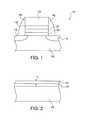
- FIG. 1depicts an edge-on view of a portion of a SONOS type semiconductor device having a blocking structure formed on a storage node;
- FIGS. 2-3depict a series of successive edge-on views for forming a portion of the structure of FIG. 1 ;
- FIG. 4depicts the structure shown in FIG. 3 being formed within a High Density Plasma (HDP) device;
- HDPHigh Density Plasma
- FIGS. 5 and 6depict charts regarding SiO 2 formation on Si and on a Si 3 N 4 substrate.
- FIG. 7depicts a chart which compares the differences between nitrogen and oxygen accumulation in atomic percentage at varying depths in a layer when using either a high density plasma oxidation process or an in-situ steam oxidation process;
- FIG. 8depicts a flowchart illustration of thickness control of Si 3 N 4 and Si by repetition of HDP oxidation and dipping in HF solution.
- the present inventionincludes a dielectric layer which is formed using a high density plasma oxidation process.
- a high density plasma oxidation processthe dielectric layer can be formed at a much lower temperature than competing deposition processes, such as chemical vapor deposition (CVD), in-situ steam oxidation (ISSG), and rapid thermal oxidation.
- CVDchemical vapor deposition
- ISSGin-situ steam oxidation
- rapid thermal oxidationThe lower temperature provides the benefit of a reduced thermal budget and prevents the distortion of certain components which are sensitive to high temperatures.
- the high density plasma oxidation processresults in a dielectric layer having a top surface which is much more uniform and smooth than that formed with competing deposition processes.
- the thickness of a layer beneath the dielectric layercan be reduced during the formation of the dielectric layer to a final thickness which is less than 20 ⁇ .
- semiconductor structuressuch as memory cells, can be formed with greater accuracy at smaller sizes.
- the inventionprovides a semiconductor device which has a higher reliability and a reduced manufacturing cost due to the lower thermal budget.
- a storage layer 130is formed on a first dielectric layer 120 , which in turn is formed on a semiconductor substrate 100 .
- the semiconductor substrate 100comprises a single crystal or polycrystalline silicon substrate, however, the semiconductor substrate 100 may comprise other materials. Suitable materials for semiconductor substrate 100 include silicon, gallium arsenide, germanium, gallium nitride, aluminum phosphide, Sil-xGex and AlxGal-xAs alloys, wherein x is greater than or equal to zero and less than or equal to one, the like, and combinations thereof. Additional examples of materials for semiconductor substrate 100 in accordance with the present invention are set forth in Semiconductor Device Fundamentals by Robert F. Pierret (p.
- the substrate 100is loaded into a HDP system to form a dielectric layer 140 on the storage layer 130 in an oxygen and/or hydrogen ambient.
- source and drain regions 110 and 112may be formed in the semiconductor substrate 100 by methods well known to those of ordinary skill in the art.
- the storage layer 130may comprise SiN, as in a SONOS type device. In one embodiment, the storage layer 130 is a floating gate.
- the dielectric layer 120may comprise silicon nitride, silicon oxynitride, or other oxides, nitrides, or oxynitrides.
- the first dielectric layer 120is formed using a high density plasma (HDP) oxidation process similar to one used to form a second dielectric layer 140 , as discussed below.
- the dielectric layer 120forms a tunneling oxide layer comprising SiO 2 , SiO 2 /Si 3 N 4 , or Si/SiO 2 .
- a second dielectric layer 140is formed on the storage layer 130 using a high density plasma (HDP) oxidation process.
- This same HDP oxidation processcan also be used to form the first dielectric layer 120 .
- this same HDP oxidation processcan also be used to form any dielectric layer described herein.
- this same HDP oxidation processcan be used to thin any silicon or nitride layer described herein by oxidizing a portion of the silicon or nitride layer described herein using HDP oxidation and removing said oxidized portion.
- the HDP oxidation processcan also be used to form control oxide layers consisting of an oxide layer on a nitride layer on an oxide layer (an ONO structure).
- the second dielectric layer 140comprises oxide, and more preferably, silicon oxide.
- the HDP oxidation processis conducted at a temperature preferably of less than 700° C., and more preferably less than 400° C. using high density plasma 170 . But the temperature can be easily controlled up to 700° C. by adjusting a bias 188 to the substrate 100 .
- the source of oxygen for the high density plasma 170may be an oxygen containing precursor, or ambient 190 , such as O 2 , O 2 , N 2 O, NO, CO, CO 2 , H 2 O or their mixture with any other inert gas (He, Ar, N, etc.), or an oxidizing gas (NO, N 2 O, O 2 , etc.).
- the high density plasma 170is also formed using a hydrogen containing precursor, or ambient 190 , such as H 2 , NH 3 , D 2 , ND 3 .
- the high density plasma 170may be generated by any one of a number of sources or HDP generating devices 176 , such as HDP CVD tools manufactured by Novellus Systems Inc. of San Jose, Calif. or Applied Materials of Santa Clara, Calif.
- sources or HDP generating devices 176such as HDP CVD tools manufactured by Novellus Systems Inc. of San Jose, Calif. or Applied Materials of Santa Clara, Calif.
- one of the following sourcesmay be used: helicon; helical-resonator; electron-cyclotron resonance; or inductively coupled plasma generator.
- the HDP generating device 176is an HDP CVD tool in the SPEED line of tools manufactured by Novellus Systems Inc., of San Jose, Calif.
- the HDP generating device 176includes a housing 177 having walls 178 surrounding and defining a chamber 171 .
- a coil 180surrounds the housing 177 and is used to generate an electromagnetic field.
- Low frequency poweris applied to the coil 180 at first through a bias 186 .
- Secondary powermay be applied to a wafer holder 182 through the bias 188 to control the temperature of the substrate 100 .
- the housing 177forms an opening 184 through which a passageway 172 is formed.
- the opening 184allows for an ambient 190 to be introduced into the chamber 171 .
- the ambient 190is later converted into high density plasma 170 in the chamber 171 .
- the semiconductor substrate 100rests on a wafer holder 182 within the chamber 171 , on which high density plasma 170 is deposited using an HDP oxidation process.
- the substrate 100can be unbiased, in which case ionized substances are accelerated by the plasma potential (on the order of 20 Volts) and then implanted into or onto the substrate 100 .
- a biascan be applied to the substrate 100 to further accelerate the ions from the high density plasma and deposit them or implant them deeper into the surface of the substrate 100 . Either a DC or RF bias may be applied to the substrate 100 .
- the following process conditionsare used by the HDP generating device 176 to create an HDP oxidation process used to form the second dielectric layer 140 .
- the HDP generating device 176is placed in an unbiased and unclamped (UBUC) mode.
- UBUCunbiased and unclamped
- a certain amount of low frequency poweris applied to the first power node 186 and a certain amount of high frequency power is applied to the second power node 188 .
- high frequency poweris applied to the first power node 186 and low frequency power is applied to the second power node 188 .
- the first power node 186is connected with the coil 180 and the second power node 188 is connected with the wafer holder 182 .
- the low frequency power appliedhas a wattage from 1000 W to 30000 W, and more preferably from 2000 W to 25000 W, and more preferably about 3000 W.
- the low frequency poweris applied having a frequency from 100 kHz to 1000 kHz, and more preferably a frequency from 200 kHz to 600 kHz, and even more preferably a frequency of 300 kHz to 500 kHz, and even more preferably about 450 kHz ⁇ 10%, and most preferably greater than 400 kHz and less than 2000 kHz.
- High frequency powermay also be applied to the coil 180 .
- no high frequency poweris applied, and more preferably high frequency power is applied having a wattage from 0 W to 50 W, and a frequency of between 12 and 14 MHz, and most preferably about 13.56 MHz.
- Ambient 190is introduced into the chamber 171 , preferably having a mixture of oxygen and hydrogen.
- the oxygenis O 2 having a flow rate from 10 sccm to 1000 sccm, and more preferably from 90 sccm to 500 sccm, and most preferably from 100 sccm to 400 sccm.
- the hydrogenis H 2 having a flow rate from 10 sccm to 1000 sccm, and more preferably from 90 sccm to 500 sccm, and most preferably from 100 sccm to 400 sccm.
- the flow rate of the O 2is within ⁇ 10% of the flow rate of the H 2 , and more preferably the flow rate of the O 2 is within ⁇ 5% of the flow rate of the H 2 , and most preferably the flow rate of the O 2 is about the same as the flow rate of the H 2 .
- the thickness t 0 of the second dielectric layer 140has good uniformity.
- the temperature of the semiconductor substrate 100 on the wafer holder 182is set in the UBUC mode to a temperature which is preferably less than 700° C., and more preferably less than 400° C., and even more preferably from 300° C. to 400° C., and even more preferably from 325° C. to 375° C., and most preferably about 350° C. ⁇ 10%.
- the temperature of the semiconductor substrate 100can later be controlled by application of bias power (i.e. ion bombardment).
- bias poweri.e. ion bombardment
- the amount of time required to run the HDP oxidation processcan vary depending on the amount of dielectric material desired for making the second dielectric layer 140 .
- the HDP oxidation processis run from 10 to 120 seconds, and more preferably from 20 to 60 seconds, and more preferably about 30 seconds ⁇ 10%.
- a portion of the layer on which the dielectric layer is formed onis oxidized.
- the dielectric layer, and the oxidized portion of the layer on which the dielectric layer is formed onare both removed.
- the second dielectric layer 140is formed on a storage layer 130 which comprises Si3N4 or SiO2, and the thickness of the storage layer 130 is reduced through oxidization of a portion of the storage layer 130 .
- the second dielectric layer 140 and the oxide formed on the storage layer 130are then removed by applying an etch, such as a hydrofluoric acid (HF) solution, to the second dielectric layer 140 , reducing the thickness of the storage layer 130 .
- an etchsuch as a hydrofluoric acid (HF) solution
- the thickness of the storage layer 130is measured upon removal of the oxidized portion, and a third dielectric layer (not shown) is formed on the storage layer 130 after the second dielectric layer 140 is removed.
- the first dielectric layer 120is formed on the semiconductor substrate 100 using the high density plasma (HDP) oxidation process discussed herein.
- the HDP oxidation processis conducted at a temperature preferably of less than 700° C. using high density plasma 170 .
- the source of oxygen for the high density plasma 170may be an oxygen containing precursor, or ambient 190 , such as of O 2 , H 2 , or their mixture with any other inert gas (He, Ar, N, etc.), or an oxidizing gas (NO, N 2 O, O 2 , etc.).
- the high density plasma 170may be generated by any one of a number of sources or HDP generating devices 176 .
- the first dielectric layer 120can be formed with a lower thermal budget than by conventional means
- the semiconductor structure 116 shown in FIG. 1is formed by patterning the first dielectric layer 120 , the storage layer 130 , and the second dielectric layer 140 to form a tunneling structure 122 from the first dielectric layer 120 , a storage node 132 from the storage layer 130 , and a blocking structure 142 from the second dielectric layer 140 .
- a gate electrode 152is formed on the blocking structure 142 and first and second sidewall spacers 160 and 162 are formed on each side of the stack of the tunneling structure 122 , the storage node 132 , the blocking structure 142 , and the gate electrode 152 , as shown in FIG. 1 .
- first and second doped regions 110 and 112can be formed in the substrate 100 .
- the semiconductor structure 116can then be placed in a semiconductor device.
- the storage node 132can be a floating gate, or can be part of a SONOS device.
- FIGS. 5 and 6depict charts regarding SiO 2 formation on Si and on a Si 3 N 4 substrate.
- FIG. 5depicts a first set of profiles which chart the oxide thickness in angstroms of either SiO 2 formed on Si 3 N 4 or SiO 2 formed on Si in relation to the flow rate of H 2 in sccm.
- FIG. 5depicts a second set of profiles which chart the thickness uniformity in percent of either SiO 2 formed on Si 3 N 4 or SiO 2 formed on Si in relation to the flow rate of H 2 in sccm.
- FIG. 5depicts a first set of profiles which chart the oxide thickness in angstroms of either SiO 2 formed on Si 3 N 4 or SiO 2 formed on Si in relation to the flow rate of H 2 in sccm.
- the HDP generating device 176used the following process conditions: a low frequency wattage of 3000 W, a time of 60 seconds, a flow rate of 100 sccm for an O 2 ambient, and a flow rate of 300 sccm for an He ambient.
- a low frequency wattage of 3000 Wused the following process conditions: a low frequency wattage of 3000 W, a time of 60 seconds, a flow rate of 100 sccm for an O 2 ambient, and a flow rate of 300 sccm for an He ambient.
- the best thickness uniformity for the dielectric layer which is formed during the process shown in FIG. 5occurs when the flow rate of the O 2 ambient equals the flow rate of an H 2 ambient.
- FIG. 6depicts a second set of profiles which chart the thickness uniformity in percent of either SiO 2 formed on Si 3 N 4 or SiO 2 formed on Si in relation to the flow rate of O 2 in sccm.
- the HDP generating device 176used the following process conditions: a low frequency wattage of 3000 W, a time of 60 seconds, a flow rate of 400 sccm for an H 2 ambient, and a flow rate of 300 sccm for an He ambient.
- the best thickness uniformity for the dielectric layer which is formed during the process shown in FIG. 6occurs when the flow rate of the O 2 ambient equals the flow rate of an H 2 ambient.
- Table Ashown below, indicates the Rms, the Ra, and the Rmax, all in angstroms, for the surface roughness of a dielectric layer formed using the above described HDP oxidation process, using an in-situ steam oxidation (ISSG) process, using an HTO process, and using an HTO+(GOX100) process.
- Table Aillustrates how the Rms, the Ra, and the Rmax, are all lowest when using the above described HDP oxidation process.
- the HDP oxidation processforms a second dielectric layer 140 with a surface roughness having a Rms of less than 2.70 ⁇ , and more preferably of less than 2.50 ⁇ , and most preferably of less than 2.20 ⁇ .
- the HDP oxidation processforms a second dielectric layer 140 with a surface roughness having a Ra of less than 2.15 ⁇ , and more preferably of less than 2.0 ⁇ , and most preferably of less than 1.75 ⁇ .
- the HDP oxidation processforms a second dielectric layer 140 with a surface roughness having a Rmax of less than 26 ⁇ , and more preferably of less than 20 ⁇ , and most preferably of less than 19 ⁇ .
- the storage layer 130whose thickness is reduced when using the HDP oxidation process, can also be formed with much more uniformity and therefore lower Rms, Ra, and Rmax values than comparable processes. As a result, the final thickness t f of the storage layer 130 can also be greatly reduced with respect to competing deposition processes.
- FIG. 7depicts a chart which compares the differences between nitrogen and oxygen accumulation in atomic percentage at varying depths in a layer, such as the storage layer 130 , when using either a high density plasma oxidation process or an in-situ steam oxidation process.
- a layersuch as the storage layer 130
- FIG. 7depicts a chart which compares the differences between nitrogen and oxygen accumulation in atomic percentage at varying depths in a layer, such as the storage layer 130 , when using either a high density plasma oxidation process or an in-situ steam oxidation process.
- FIG. 8depicts a flowchart illustration of oxide formation on a dielectric using a high density plasma oxidation process.
- a determinationis made as to what type of structure is to be formed, either an ONO structure having a second dielectric layer 140 on a storage layer 130 comprising nitride on a first dielectric layer 120 , or an OSO structure in which the storage layer 130 comprises silicon.
- a second dielectric layer 140is formed on the storage layer 130 using the above described HDP oxidation process.
- the HDP oxidation processalso thins the storage layer 130 .
- oxide from the second dielectric layer 140is removed, preferably using a hydrofluoric acid solution.
- the thickness of the storage layer 130is measured. If the thickness is sufficient, then the process moves to 340 ; if the thickness is insufficient, then the process moves back to 310 .
- a final dielectric layeris formed on the storage layer 130 to form a quantumized stacked layer having either an ONO structure or an OSO structure.
- each of the layers of either the ONO structure or the OSO structureis less than 50 angstroms thick, and more preferably less than 20 angstroms thick.
Landscapes
- Engineering & Computer Science (AREA)
- Physics & Mathematics (AREA)
- Condensed Matter Physics & Semiconductors (AREA)
- General Physics & Mathematics (AREA)
- Manufacturing & Machinery (AREA)
- Computer Hardware Design (AREA)
- Microelectronics & Electronic Packaging (AREA)
- Power Engineering (AREA)
- Semiconductor Memories (AREA)
- Formation Of Insulating Films (AREA)
Abstract
Description
| TABLE A | |||||
| HDP | ON with | ||||
| Oxidized | ON with | HTO + | |||
| ON | HTO | (GOX100) | |||
| Rms | 2.15 | 3.02 | 2.91 | ||
| (A) | (−26%) | (+4%) | (0%) | ||
| Ra | 1.70 | 2.39 | 2.29 | ||
| (A) | (−26%) | (+4%) | (0%) | ||
| Rmax | 18.18 | 26.86 | 29.42 | ||
| (A) | (−38%) | (−9%) | (0%) | ||
Claims (15)
Priority Applications (7)
| Application Number | Priority Date | Filing Date | Title |
|---|---|---|---|
| US11/836,683US8119538B1 (en) | 2007-08-09 | 2007-08-09 | Oxide formation in a plasma process |
| US13/401,712US8822349B1 (en) | 2007-08-09 | 2012-02-21 | Oxide formation in a plasma process |
| US14/562,462US9406574B1 (en) | 2007-08-09 | 2014-12-05 | Oxide formation in a plasma process |
| US14/969,468US9460974B1 (en) | 2007-08-09 | 2015-12-15 | Oxide formation in a plasma process |
| US15/266,239US10128258B2 (en) | 2007-08-09 | 2016-09-15 | Oxide formation in a plasma process |
| US16/135,897US10319733B2 (en) | 2007-08-09 | 2018-09-19 | Oxide formation in a plasma process |
| US16/434,856US20200161324A1 (en) | 2007-08-09 | 2019-06-07 | Oxide formation in a plasma process |
Applications Claiming Priority (1)
| Application Number | Priority Date | Filing Date | Title |
|---|---|---|---|
| US11/836,683US8119538B1 (en) | 2007-08-09 | 2007-08-09 | Oxide formation in a plasma process |
Related Child Applications (1)
| Application Number | Title | Priority Date | Filing Date |
|---|---|---|---|
| US13/401,712ContinuationUS8822349B1 (en) | 2007-08-09 | 2012-02-21 | Oxide formation in a plasma process |
Publications (1)
| Publication Number | Publication Date |
|---|---|
| US8119538B1true US8119538B1 (en) | 2012-02-21 |
Family
ID=45571996
Family Applications (2)
| Application Number | Title | Priority Date | Filing Date |
|---|---|---|---|
| US11/836,683Active2029-02-07US8119538B1 (en) | 2007-08-09 | 2007-08-09 | Oxide formation in a plasma process |
| US13/401,712ActiveUS8822349B1 (en) | 2007-08-09 | 2012-02-21 | Oxide formation in a plasma process |
Family Applications After (1)
| Application Number | Title | Priority Date | Filing Date |
|---|---|---|---|
| US13/401,712ActiveUS8822349B1 (en) | 2007-08-09 | 2012-02-21 | Oxide formation in a plasma process |
Country Status (1)
| Country | Link |
|---|---|
| US (2) | US8119538B1 (en) |
Cited By (4)
| Publication number | Priority date | Publication date | Assignee | Title |
|---|---|---|---|---|
| US20090170282A1 (en)* | 2007-12-28 | 2009-07-02 | Cha Deok Dong | Method of Forming Isolation Layer in Semiconductor Device |
| US9460974B1 (en) | 2007-08-09 | 2016-10-04 | Cypress Semiconductor Corporation | Oxide formation in a plasma process |
| US9679980B2 (en) | 2014-03-13 | 2017-06-13 | Taiwan Semiconductor Manufacturing Co., Ltd. | Common source oxide formation by in-situ steam oxidation for embedded flash |
| CN114765184A (en)* | 2021-01-13 | 2022-07-19 | 联华电子股份有限公司 | Memory structure and manufacturing method thereof |
Citations (10)
| Publication number | Priority date | Publication date | Assignee | Title |
|---|---|---|---|---|
| US5434109A (en)* | 1993-04-27 | 1995-07-18 | International Business Machines Corporation | Oxidation of silicon nitride in semiconductor devices |
| US6271112B1 (en)* | 1998-11-13 | 2001-08-07 | Advanced Micro Devices, Inc. | Interlayer between titanium nitride and high density plasma oxide |
| US20020004277A1 (en)* | 2000-02-28 | 2002-01-10 | Micron Technology, Inc. | Structure and method for dual gate oxide thicknesses |
| US6458650B1 (en)* | 2001-07-20 | 2002-10-01 | Taiwan Semiconductor Manufacturing Company | CU second electrode process with in situ ashing and oxidation process |
| US20030026158A1 (en)* | 2001-07-30 | 2003-02-06 | Matrix Semiconductor, Inc. | Anti-fuse memory cell with asymmetric breakdown voltage |
| US20050260107A1 (en)* | 2003-07-01 | 2005-11-24 | Jackson David P | Method, process, chemistry and apparatus for treating a substrate |
| US20070249127A1 (en)* | 2006-04-24 | 2007-10-25 | Freescale Semiconductor, Inc. | Electronic device including a semiconductor layer and a sidewall spacer and a process of forming the same |
| US20080014718A1 (en)* | 2006-07-13 | 2008-01-17 | S.O.I Tec Silicon On Insulator Technologies S.A. | Treatment for bonding interface stabilization |
| US20080251833A1 (en)* | 2007-04-12 | 2008-10-16 | Michael Specht | Integrated circuits and methods of manufacture |
| US20080296655A1 (en)* | 2007-05-31 | 2008-12-04 | United Microelectronics Corp. | Multi-time programmable memory and method of manufacturing the same |
Family Cites Families (3)
| Publication number | Priority date | Publication date | Assignee | Title |
|---|---|---|---|---|
| US6559036B1 (en)* | 1998-08-07 | 2003-05-06 | Semiconductor Energy Laboratory Co., Ltd. | Semiconductor device and method of manufacturing the same |
| US7381595B2 (en)* | 2004-03-15 | 2008-06-03 | Sharp Laboratories Of America, Inc. | High-density plasma oxidation for enhanced gate oxide performance |
| KR100514526B1 (en)* | 2003-10-08 | 2005-09-13 | 동부아남반도체 주식회사 | Semiconductor device and fabricating method thereof |
- 2007
- 2007-08-09USUS11/836,683patent/US8119538B1/enactiveActive
- 2012
- 2012-02-21USUS13/401,712patent/US8822349B1/enactiveActive
Patent Citations (10)
| Publication number | Priority date | Publication date | Assignee | Title |
|---|---|---|---|---|
| US5434109A (en)* | 1993-04-27 | 1995-07-18 | International Business Machines Corporation | Oxidation of silicon nitride in semiconductor devices |
| US6271112B1 (en)* | 1998-11-13 | 2001-08-07 | Advanced Micro Devices, Inc. | Interlayer between titanium nitride and high density plasma oxide |
| US20020004277A1 (en)* | 2000-02-28 | 2002-01-10 | Micron Technology, Inc. | Structure and method for dual gate oxide thicknesses |
| US6458650B1 (en)* | 2001-07-20 | 2002-10-01 | Taiwan Semiconductor Manufacturing Company | CU second electrode process with in situ ashing and oxidation process |
| US20030026158A1 (en)* | 2001-07-30 | 2003-02-06 | Matrix Semiconductor, Inc. | Anti-fuse memory cell with asymmetric breakdown voltage |
| US20050260107A1 (en)* | 2003-07-01 | 2005-11-24 | Jackson David P | Method, process, chemistry and apparatus for treating a substrate |
| US20070249127A1 (en)* | 2006-04-24 | 2007-10-25 | Freescale Semiconductor, Inc. | Electronic device including a semiconductor layer and a sidewall spacer and a process of forming the same |
| US20080014718A1 (en)* | 2006-07-13 | 2008-01-17 | S.O.I Tec Silicon On Insulator Technologies S.A. | Treatment for bonding interface stabilization |
| US20080251833A1 (en)* | 2007-04-12 | 2008-10-16 | Michael Specht | Integrated circuits and methods of manufacture |
| US20080296655A1 (en)* | 2007-05-31 | 2008-12-04 | United Microelectronics Corp. | Multi-time programmable memory and method of manufacturing the same |
Cited By (7)
| Publication number | Priority date | Publication date | Assignee | Title |
|---|---|---|---|---|
| US9460974B1 (en) | 2007-08-09 | 2016-10-04 | Cypress Semiconductor Corporation | Oxide formation in a plasma process |
| US10128258B2 (en) | 2007-08-09 | 2018-11-13 | Cypress Semiconductor Corporation | Oxide formation in a plasma process |
| US10319733B2 (en) | 2007-08-09 | 2019-06-11 | Cypress Semiconductor Corporation | Oxide formation in a plasma process |
| US20090170282A1 (en)* | 2007-12-28 | 2009-07-02 | Cha Deok Dong | Method of Forming Isolation Layer in Semiconductor Device |
| US8343846B2 (en)* | 2007-12-28 | 2013-01-01 | Cha Deok Dong | Method of forming isolation layer in semiconductor device |
| US9679980B2 (en) | 2014-03-13 | 2017-06-13 | Taiwan Semiconductor Manufacturing Co., Ltd. | Common source oxide formation by in-situ steam oxidation for embedded flash |
| CN114765184A (en)* | 2021-01-13 | 2022-07-19 | 联华电子股份有限公司 | Memory structure and manufacturing method thereof |
Also Published As
| Publication number | Publication date |
|---|---|
| US8822349B1 (en) | 2014-09-02 |
Similar Documents
| Publication | Publication Date | Title |
|---|---|---|
| US7071122B2 (en) | Field effect transistor with etched-back gate dielectric | |
| US9431237B2 (en) | Post treatment methods for oxide layers on semiconductor devices | |
| US10319733B2 (en) | Oxide formation in a plasma process | |
| US7910497B2 (en) | Method of forming dielectric layers on a substrate and apparatus therefor | |
| US7964514B2 (en) | Multiple nitrogen plasma treatments for thin SiON dielectrics | |
| US7837838B2 (en) | Method of fabricating a high dielectric constant transistor gate using a low energy plasma apparatus | |
| US6780720B2 (en) | Method for fabricating a nitrided silicon-oxide gate dielectric | |
| EP0973189A2 (en) | A method for gate-stack formation including a high-K dielectric | |
| US7645709B2 (en) | Methods for low temperature oxidation of a semiconductor device | |
| CN101652843B (en) | Method for forming silicon nitride film, method for manufacturing nonvolatile semiconductor memory device, nonvolatile semiconductor memory device and plasma processing apparatus | |
| US20060110939A1 (en) | Enhanced thin-film oxidation process | |
| EP1923910A2 (en) | Selective removal of rare earth comprising materials in a semiconductor device | |
| US20070209930A1 (en) | Apparatus for fabricating a high dielectric constant transistor gate using a low energy plasma system | |
| CN101401194B (en) | Method and apparatus for fabricating high dielectric constant transistor gates using a low energy plasma system | |
| CN107735851A (en) | It is used for spacer deposition and the apparatus and method for selectively removed in advanced Patternized technique | |
| US9780000B2 (en) | Method for forming spacers for a transitor gate | |
| CN101620995A (en) | Gate dielectric layer, manufacturing method thereof, semiconductor device and manufacturing method thereof | |
| US8822349B1 (en) | Oxide formation in a plasma process | |
| US6998303B2 (en) | Manufacture method for semiconductor device with patterned film of ZrO2 or the like | |
| US6821904B2 (en) | Method of blocking nitrogen from thick gate oxide during dual gate CMP | |
| US8163626B2 (en) | Enhancing NAND flash floating gate performance | |
| US9698043B1 (en) | Shallow trench isolation for semiconductor devices | |
| US7491622B2 (en) | Process of forming an electronic device including a layer formed using an inductively coupled plasma | |
| US6939816B2 (en) | Method to improve the uniformity and reduce the surface roughness of the silicon dielectric interface | |
| US11804380B2 (en) | High-throughput dry etching of films containing silicon-oxygen components or silicon-nitrogen components by proton-mediated catalyst formation |
Legal Events
| Date | Code | Title | Description |
|---|---|---|---|
| AS | Assignment | Owner name:CYPRESS SEMICONDUCTOR CORPORATION, CALIFORNIA Free format text:ASSIGNMENT OF ASSIGNORS INTEREST;ASSIGNORS:BYUN, JEONG SOO;RAMKUMAR, KRISHNASWAMY;REEL/FRAME:019675/0025 Effective date:20070809 | |
| STCF | Information on status: patent grant | Free format text:PATENTED CASE | |
| AS | Assignment | Owner name:MORGAN STANLEY SENIOR FUNDING, INC., NEW YORK Free format text:SECURITY INTEREST;ASSIGNORS:CYPRESS SEMICONDUCTOR CORPORATION;SPANSION LLC;REEL/FRAME:035240/0429 Effective date:20150312 | |
| FPAY | Fee payment | Year of fee payment:4 | |
| AS | Assignment | Owner name:LONGITUDE FLASH MEMORY SOLUTIONS LTD., IRELAND Free format text:ASSIGNMENT OF ASSIGNORS INTEREST;ASSIGNOR:CYPRESS SEMICONDUCTOR CORPORATION;REEL/FRAME:049086/0803 Effective date:20190503 | |
| AS | Assignment | Owner name:SPANSION LLC, CALIFORNIA Free format text:RELEASE BY SECURED PARTY;ASSIGNOR:MORGAN STANLEY SENIOR FUNDING, INC.;REEL/FRAME:049109/0573 Effective date:20190503 Owner name:CYPRESS SEMICONDUCTOR CORPORATION, CALIFORNIA Free format text:RELEASE BY SECURED PARTY;ASSIGNOR:MORGAN STANLEY SENIOR FUNDING, INC.;REEL/FRAME:049109/0573 Effective date:20190503 | |
| MAFP | Maintenance fee payment | Free format text:PAYMENT OF MAINTENANCE FEE, 8TH YEAR, LARGE ENTITY (ORIGINAL EVENT CODE: M1552); ENTITY STATUS OF PATENT OWNER: LARGE ENTITY Year of fee payment:8 | |
| AS | Assignment | Owner name:MORGAN STANLEY SENIOR FUNDING, INC., NEW YORK Free format text:CORRECTIVE ASSIGNMENT TO CORRECT THE 8647899 PREVIOUSLY RECORDED ON REEL 035240 FRAME 0429. ASSIGNOR(S) HEREBY CONFIRMS THE SECURITY INTERST;ASSIGNORS:CYPRESS SEMICONDUCTOR CORPORATION;SPANSION LLC;REEL/FRAME:058002/0470 Effective date:20150312 | |
| MAFP | Maintenance fee payment | Free format text:PAYMENT OF MAINTENANCE FEE, 12TH YEAR, LARGE ENTITY (ORIGINAL EVENT CODE: M1553); ENTITY STATUS OF PATENT OWNER: LARGE ENTITY Year of fee payment:12 |