US8119513B1 - Method for making cadmium sulfide layer - Google Patents
Method for making cadmium sulfide layerDownload PDFInfo
- Publication number
- US8119513B1 US8119513B1US12/951,108US95110810AUS8119513B1US 8119513 B1US8119513 B1US 8119513B1US 95110810 AUS95110810 AUS 95110810AUS 8119513 B1US8119513 B1US 8119513B1
- Authority
- US
- United States
- Prior art keywords
- layer
- cadmium
- substrate
- transparent
- sulfide
- Prior art date
- Legal status (The legal status is an assumption and is not a legal conclusion. Google has not performed a legal analysis and makes no representation as to the accuracy of the status listed.)
- Expired - Fee Related
Links
- 229910052980cadmium sulfideInorganic materials0.000titleclaimsabstractdescription48
- 238000000034methodMethods0.000titleclaimsabstractdescription48
- WUPHOULIZUERAE-UHFFFAOYSA-N3-(oxolan-2-yl)propanoic acidChemical compoundOC(=O)CCC1CCCO1WUPHOULIZUERAE-UHFFFAOYSA-N0.000titleclaimsabstractdescription45
- BDOSMKKIYDKNTQ-UHFFFAOYSA-Ncadmium atomChemical compound[Cd]BDOSMKKIYDKNTQ-UHFFFAOYSA-N0.000claimsabstractdescription49
- 229910052793cadmiumInorganic materials0.000claimsabstractdescription45
- 239000000758substrateSubstances0.000claimsabstractdescription32
- 238000005987sulfurization reactionMethods0.000claimsabstractdescription18
- 238000004544sputter depositionMethods0.000claimsdescription19
- 238000000151depositionMethods0.000claimsdescription9
- 230000008021depositionEffects0.000claimsdescription8
- 238000004519manufacturing processMethods0.000claimsdescription8
- 229910052717sulfurInorganic materials0.000claimsdescription8
- XLOMVQKBTHCTTD-UHFFFAOYSA-NZinc monoxideChemical compound[Zn]=OXLOMVQKBTHCTTD-UHFFFAOYSA-N0.000claimsdescription7
- 229910052760oxygenInorganic materials0.000claimsdescription7
- NINIDFKCEFEMDL-UHFFFAOYSA-NSulfurChemical compound[S]NINIDFKCEFEMDL-UHFFFAOYSA-N0.000claimsdescription6
- QVGXLLKOCUKJST-UHFFFAOYSA-Natomic oxygenChemical compound[O]QVGXLLKOCUKJST-UHFFFAOYSA-N0.000claimsdescription6
- 239000001301oxygenSubstances0.000claimsdescription6
- 239000011593sulfurSubstances0.000claimsdescription6
- 229910052782aluminiumInorganic materials0.000claimsdescription5
- 239000010949copperSubstances0.000claimsdescription5
- UCKMPCXJQFINFW-UHFFFAOYSA-NSulphideChemical compound[S-2]UCKMPCXJQFINFW-UHFFFAOYSA-N0.000claimsdescription4
- 229910052733galliumInorganic materials0.000claimsdescription4
- 239000007789gasSubstances0.000claimsdescription4
- 229910052738indiumInorganic materials0.000claimsdescription4
- APFVFJFRJDLVQX-UHFFFAOYSA-Nindium atomChemical compound[In]APFVFJFRJDLVQX-UHFFFAOYSA-N0.000claimsdescription4
- 239000011669seleniumSubstances0.000claimsdescription4
- XOLBLPGZBRYERU-UHFFFAOYSA-Ntin dioxideChemical compoundO=[Sn]=OXOLBLPGZBRYERU-UHFFFAOYSA-N0.000claimsdescription4
- 229910001887tin oxideInorganic materials0.000claimsdescription4
- RYGMFSIKBFXOCR-UHFFFAOYSA-NCopperChemical compound[Cu]RYGMFSIKBFXOCR-UHFFFAOYSA-N0.000claimsdescription3
- RWSOTUBLDIXVET-UHFFFAOYSA-NDihydrogen sulfideChemical compoundSRWSOTUBLDIXVET-UHFFFAOYSA-N0.000claimsdescription3
- 229910018503SF6Inorganic materials0.000claimsdescription3
- -1alkane thiolsChemical class0.000claimsdescription3
- XAGFODPZIPBFFR-UHFFFAOYSA-NaluminiumChemical compound[Al]XAGFODPZIPBFFR-UHFFFAOYSA-N0.000claimsdescription3
- 229910052802copperInorganic materials0.000claimsdescription3
- 239000011521glassSubstances0.000claimsdescription3
- 229910000037hydrogen sulfideInorganic materials0.000claimsdescription3
- 238000001771vacuum depositionMethods0.000claimsdescription3
- 239000011787zinc oxideSubstances0.000claimsdescription3
- GYHNNYVSQQEPJS-UHFFFAOYSA-NGalliumChemical compound[Ga]GYHNNYVSQQEPJS-UHFFFAOYSA-N0.000claimsdescription2
- BUGBHKTXTAQXES-UHFFFAOYSA-NSeleniumChemical compound[Se]BUGBHKTXTAQXES-UHFFFAOYSA-N0.000claimsdescription2
- BQCADISMDOOEFD-UHFFFAOYSA-NSilverChemical compound[Ag]BQCADISMDOOEFD-UHFFFAOYSA-N0.000claimsdescription2
- ATJFFYVFTNAWJD-UHFFFAOYSA-NTinChemical compound[Sn]ATJFFYVFTNAWJD-UHFFFAOYSA-N0.000claimsdescription2
- HCHKCACWOHOZIP-UHFFFAOYSA-NZincChemical compound[Zn]HCHKCACWOHOZIP-UHFFFAOYSA-N0.000claimsdescription2
- QGJOPFRUJISHPQ-NJFSPNSNSA-Ncarbon disulfide-14cChemical compoundS=[14C]=SQGJOPFRUJISHPQ-NJFSPNSNSA-N0.000claimsdescription2
- 238000005328electron beam physical vapour depositionMethods0.000claimsdescription2
- 230000008020evaporationEffects0.000claimsdescription2
- 238000001704evaporationMethods0.000claimsdescription2
- 238000004549pulsed laser depositionMethods0.000claimsdescription2
- 229910052711seleniumInorganic materials0.000claimsdescription2
- 229910052709silverInorganic materials0.000claimsdescription2
- 239000004332silverSubstances0.000claimsdescription2
- FWMUJAIKEJWSSY-UHFFFAOYSA-Nsulfur dichlorideChemical compoundClSClFWMUJAIKEJWSSY-UHFFFAOYSA-N0.000claimsdescription2
- SFZCNBIFKDRMGX-UHFFFAOYSA-Nsulfur hexafluorideChemical compoundFS(F)(F)(F)(F)FSFZCNBIFKDRMGX-UHFFFAOYSA-N0.000claimsdescription2
- 229960000909sulfur hexafluorideDrugs0.000claimsdescription2
- XSOKHXFFCGXDJZ-UHFFFAOYSA-Ntelluride(2-)Chemical compound[Te-2]XSOKHXFFCGXDJZ-UHFFFAOYSA-N0.000claimsdescription2
- 150000003568thioethersChemical class0.000claimsdescription2
- 239000011135tinSubstances0.000claimsdescription2
- 229910052718tinInorganic materials0.000claimsdescription2
- 229910052725zincInorganic materials0.000claimsdescription2
- 239000011701zincSubstances0.000claimsdescription2
- 239000000463materialSubstances0.000description11
- 239000010408filmSubstances0.000description8
- MARUHZGHZWCEQU-UHFFFAOYSA-N5-phenyl-2h-tetrazoleChemical compoundC1=CC=CC=C1C1=NNN=N1MARUHZGHZWCEQU-UHFFFAOYSA-N0.000description7
- 239000006096absorbing agentSubstances0.000description7
- 238000010586diagramMethods0.000description6
- 239000010409thin filmSubstances0.000description6
- 230000008569processEffects0.000description4
- 238000005507sprayingMethods0.000description4
- 239000000126substanceSubstances0.000description4
- VYPSYNLAJGMNEJ-UHFFFAOYSA-NSilicium dioxideChemical compoundO=[Si]=OVYPSYNLAJGMNEJ-UHFFFAOYSA-N0.000description3
- 238000006243chemical reactionMethods0.000description3
- WILFBXOGIULNAF-UHFFFAOYSA-Ncopper sulfanylidenetin zincChemical compound[Sn]=S.[Zn].[Cu]WILFBXOGIULNAF-UHFFFAOYSA-N0.000description3
- 230000006870functionEffects0.000description3
- 239000004065semiconductorSubstances0.000description3
- XKRFYHLGVUSROY-UHFFFAOYSA-NArgonChemical compound[Ar]XKRFYHLGVUSROY-UHFFFAOYSA-N0.000description2
- 229910020923Sn-OInorganic materials0.000description2
- GWEVSGVZZGPLCZ-UHFFFAOYSA-NTitan oxideChemical compoundO=[Ti]=OGWEVSGVZZGPLCZ-UHFFFAOYSA-N0.000description2
- 150000001661cadmiumChemical class0.000description2
- 238000000224chemical solution depositionMethods0.000description2
- 238000000354decomposition reactionMethods0.000description2
- 239000003989dielectric materialSubstances0.000description2
- 230000005611electricityEffects0.000description2
- 238000004070electrodepositionMethods0.000description2
- 238000011065in-situ storageMethods0.000description2
- 229910052751metalInorganic materials0.000description2
- 239000002184metalSubstances0.000description2
- 230000004048modificationEffects0.000description2
- 238000012986modificationMethods0.000description2
- 230000005855radiationEffects0.000description2
- 238000009718spray depositionMethods0.000description2
- 238000002207thermal evaporationMethods0.000description2
- BNEMLSQAJOPTGK-UHFFFAOYSA-Nzinc;dioxido(oxo)tinChemical compound[Zn+2].[O-][Sn]([O-])=OBNEMLSQAJOPTGK-UHFFFAOYSA-N0.000description2
- 229910005540GaPInorganic materials0.000description1
- GPXJNWSHGFTCBW-UHFFFAOYSA-NIndium phosphideChemical compound[In]#PGPXJNWSHGFTCBW-UHFFFAOYSA-N0.000description1
- 239000004642PolyimideSubstances0.000description1
- 229910007696ZnSnO4Inorganic materials0.000description1
- 229910007611Zn—In—OInorganic materials0.000description1
- 229910052786argonInorganic materials0.000description1
- 230000004888barrier functionEffects0.000description1
- LHQLJMJLROMYRN-UHFFFAOYSA-Lcadmium acetateChemical compound[Cd+2].CC([O-])=O.CC([O-])=OLHQLJMJLROMYRN-UHFFFAOYSA-L0.000description1
- XIEPJMXMMWZAAV-UHFFFAOYSA-Ncadmium nitrateInorganic materials[Cd+2].[O-][N+]([O-])=O.[O-][N+]([O-])=OXIEPJMXMMWZAAV-UHFFFAOYSA-N0.000description1
- CXKCTMHTOKXKQT-UHFFFAOYSA-Ncadmium oxideInorganic materials[Cd]=OCXKCTMHTOKXKQT-UHFFFAOYSA-N0.000description1
- RMCKOIXJLDOSOT-UHFFFAOYSA-Lcadmium(2+);oxalateChemical compound[Cd+2].[O-]C(=O)C([O-])=ORMCKOIXJLDOSOT-UHFFFAOYSA-L0.000description1
- CFEAAQFZALKQPA-UHFFFAOYSA-Ncadmium(2+);oxygen(2-)Chemical compound[O-2].[Cd+2]CFEAAQFZALKQPA-UHFFFAOYSA-N0.000description1
- BEQNOZDXPONEMR-UHFFFAOYSA-Ncadmium;oxotinChemical compound[Cd].[Sn]=OBEQNOZDXPONEMR-UHFFFAOYSA-N0.000description1
- 230000008859changeEffects0.000description1
- 238000000576coating methodMethods0.000description1
- 229910052681coesiteInorganic materials0.000description1
- 238000009833condensationMethods0.000description1
- 230000005494condensationEffects0.000description1
- 239000004020conductorSubstances0.000description1
- 238000011109contaminationMethods0.000description1
- 229910052906cristobaliteInorganic materials0.000description1
- 238000009792diffusion processMethods0.000description1
- WRQGPGZATPOHHX-UHFFFAOYSA-Nethyl 2-oxohexanoateChemical compoundCCCCC(=O)C(=O)OCCWRQGPGZATPOHHX-UHFFFAOYSA-N0.000description1
- HZXMRANICFIONG-UHFFFAOYSA-Ngallium phosphideChemical compound[Ga]#PHZXMRANICFIONG-UHFFFAOYSA-N0.000description1
- 238000007373indentationMethods0.000description1
- AMGQUBHHOARCQH-UHFFFAOYSA-Nindium;oxotinChemical compound[In].[Sn]=OAMGQUBHHOARCQH-UHFFFAOYSA-N0.000description1
- 238000009776industrial productionMethods0.000description1
- 150000002500ionsChemical class0.000description1
- 238000011031large-scale manufacturing processMethods0.000description1
- 229910052976metal sulfideInorganic materials0.000description1
- 125000002524organometallic groupChemical group0.000description1
- 238000007254oxidation reactionMethods0.000description1
- KYKLWYKWCAYAJY-UHFFFAOYSA-Noxotin;zincChemical compound[Zn].[Sn]=OKYKLWYKWCAYAJY-UHFFFAOYSA-N0.000description1
- NMHMNPHRMNGLLB-UHFFFAOYSA-Nphloretic acidChemical compoundOC(=O)CCC1=CC=C(O)C=C1NMHMNPHRMNGLLB-UHFFFAOYSA-N0.000description1
- 229920001721polyimidePolymers0.000description1
- 229920000642polymerPolymers0.000description1
- 239000002243precursorSubstances0.000description1
- 230000035484reaction timeEffects0.000description1
- 239000000377silicon dioxideSubstances0.000description1
- 229910052814silicon oxideInorganic materials0.000description1
- 229940071182stannateDrugs0.000description1
- 229910052682stishoviteInorganic materials0.000description1
- 238000005979thermal decomposition reactionMethods0.000description1
- 238000007736thin film deposition techniqueMethods0.000description1
- 239000004408titanium dioxideSubstances0.000description1
- 230000009466transformationEffects0.000description1
- 229910052905tridymiteInorganic materials0.000description1
Images


Classifications
- H—ELECTRICITY
- H10—SEMICONDUCTOR DEVICES; ELECTRIC SOLID-STATE DEVICES NOT OTHERWISE PROVIDED FOR
- H10F—INORGANIC SEMICONDUCTOR DEVICES SENSITIVE TO INFRARED RADIATION, LIGHT, ELECTROMAGNETIC RADIATION OF SHORTER WAVELENGTH OR CORPUSCULAR RADIATION
- H10F77/00—Constructional details of devices covered by this subclass
- H10F77/10—Semiconductor bodies
- H10F77/12—Active materials
- H10F77/123—Active materials comprising only Group II-VI materials, e.g. CdS, ZnS or HgCdTe
- H—ELECTRICITY
- H10—SEMICONDUCTOR DEVICES; ELECTRIC SOLID-STATE DEVICES NOT OTHERWISE PROVIDED FOR
- H10F—INORGANIC SEMICONDUCTOR DEVICES SENSITIVE TO INFRARED RADIATION, LIGHT, ELECTROMAGNETIC RADIATION OF SHORTER WAVELENGTH OR CORPUSCULAR RADIATION
- H10F10/00—Individual photovoltaic cells, e.g. solar cells
- H10F10/10—Individual photovoltaic cells, e.g. solar cells having potential barriers
- H10F10/16—Photovoltaic cells having only PN heterojunction potential barriers
- H10F10/162—Photovoltaic cells having only PN heterojunction potential barriers comprising only Group II-VI materials, e.g. CdS/CdTe photovoltaic cells
- H—ELECTRICITY
- H10—SEMICONDUCTOR DEVICES; ELECTRIC SOLID-STATE DEVICES NOT OTHERWISE PROVIDED FOR
- H10F—INORGANIC SEMICONDUCTOR DEVICES SENSITIVE TO INFRARED RADIATION, LIGHT, ELECTROMAGNETIC RADIATION OF SHORTER WAVELENGTH OR CORPUSCULAR RADIATION
- H10F10/00—Individual photovoltaic cells, e.g. solar cells
- H10F10/10—Individual photovoltaic cells, e.g. solar cells having potential barriers
- H10F10/16—Photovoltaic cells having only PN heterojunction potential barriers
- H10F10/167—Photovoltaic cells having only PN heterojunction potential barriers comprising Group I-III-VI materials, e.g. CdS/CuInSe2 [CIS] heterojunction photovoltaic cells
- H—ELECTRICITY
- H10—SEMICONDUCTOR DEVICES; ELECTRIC SOLID-STATE DEVICES NOT OTHERWISE PROVIDED FOR
- H10F—INORGANIC SEMICONDUCTOR DEVICES SENSITIVE TO INFRARED RADIATION, LIGHT, ELECTROMAGNETIC RADIATION OF SHORTER WAVELENGTH OR CORPUSCULAR RADIATION
- H10F71/00—Manufacture or treatment of devices covered by this subclass
- H10F71/125—The active layers comprising only Group II-VI materials, e.g. CdS, ZnS or CdTe
- H10F71/1257—The active layers comprising only Group II-VI materials, e.g. CdS, ZnS or CdTe comprising growth substrates not made of Group II-VI materials
- H—ELECTRICITY
- H10—SEMICONDUCTOR DEVICES; ELECTRIC SOLID-STATE DEVICES NOT OTHERWISE PROVIDED FOR
- H10F—INORGANIC SEMICONDUCTOR DEVICES SENSITIVE TO INFRARED RADIATION, LIGHT, ELECTROMAGNETIC RADIATION OF SHORTER WAVELENGTH OR CORPUSCULAR RADIATION
- H10F77/00—Constructional details of devices covered by this subclass
- H10F77/10—Semiconductor bodies
- H10F77/16—Material structures, e.g. crystalline structures, film structures or crystal plane orientations
- H10F77/169—Thin semiconductor films on metallic or insulating substrates
- H10F77/1694—Thin semiconductor films on metallic or insulating substrates the films including Group I-III-VI materials, e.g. CIS or CIGS
- H—ELECTRICITY
- H10—SEMICONDUCTOR DEVICES; ELECTRIC SOLID-STATE DEVICES NOT OTHERWISE PROVIDED FOR
- H10F—INORGANIC SEMICONDUCTOR DEVICES SENSITIVE TO INFRARED RADIATION, LIGHT, ELECTROMAGNETIC RADIATION OF SHORTER WAVELENGTH OR CORPUSCULAR RADIATION
- H10F77/00—Constructional details of devices covered by this subclass
- H10F77/10—Semiconductor bodies
- H10F77/16—Material structures, e.g. crystalline structures, film structures or crystal plane orientations
- H10F77/169—Thin semiconductor films on metallic or insulating substrates
- H10F77/1696—Thin semiconductor films on metallic or insulating substrates the films including Group II-VI materials, e.g. CdTe or CdS
- Y—GENERAL TAGGING OF NEW TECHNOLOGICAL DEVELOPMENTS; GENERAL TAGGING OF CROSS-SECTIONAL TECHNOLOGIES SPANNING OVER SEVERAL SECTIONS OF THE IPC; TECHNICAL SUBJECTS COVERED BY FORMER USPC CROSS-REFERENCE ART COLLECTIONS [XRACs] AND DIGESTS
- Y02—TECHNOLOGIES OR APPLICATIONS FOR MITIGATION OR ADAPTATION AGAINST CLIMATE CHANGE
- Y02E—REDUCTION OF GREENHOUSE GAS [GHG] EMISSIONS, RELATED TO ENERGY GENERATION, TRANSMISSION OR DISTRIBUTION
- Y02E10/00—Energy generation through renewable energy sources
- Y02E10/50—Photovoltaic [PV] energy
- Y02E10/541—CuInSe2 material PV cells
- Y—GENERAL TAGGING OF NEW TECHNOLOGICAL DEVELOPMENTS; GENERAL TAGGING OF CROSS-SECTIONAL TECHNOLOGIES SPANNING OVER SEVERAL SECTIONS OF THE IPC; TECHNICAL SUBJECTS COVERED BY FORMER USPC CROSS-REFERENCE ART COLLECTIONS [XRACs] AND DIGESTS
- Y02—TECHNOLOGIES OR APPLICATIONS FOR MITIGATION OR ADAPTATION AGAINST CLIMATE CHANGE
- Y02E—REDUCTION OF GREENHOUSE GAS [GHG] EMISSIONS, RELATED TO ENERGY GENERATION, TRANSMISSION OR DISTRIBUTION
- Y02E10/00—Energy generation through renewable energy sources
- Y02E10/50—Photovoltaic [PV] energy
- Y02E10/543—Solar cells from Group II-VI materials
- Y—GENERAL TAGGING OF NEW TECHNOLOGICAL DEVELOPMENTS; GENERAL TAGGING OF CROSS-SECTIONAL TECHNOLOGIES SPANNING OVER SEVERAL SECTIONS OF THE IPC; TECHNICAL SUBJECTS COVERED BY FORMER USPC CROSS-REFERENCE ART COLLECTIONS [XRACs] AND DIGESTS
- Y02—TECHNOLOGIES OR APPLICATIONS FOR MITIGATION OR ADAPTATION AGAINST CLIMATE CHANGE
- Y02P—CLIMATE CHANGE MITIGATION TECHNOLOGIES IN THE PRODUCTION OR PROCESSING OF GOODS
- Y02P70/00—Climate change mitigation technologies in the production process for final industrial or consumer products
- Y02P70/50—Manufacturing or production processes characterised by the final manufactured product
Definitions
- the inventionrelates generally to a method of making cadmium sulfide.
- the inventionrelates to method of making cadmium sulfide layers used, for example, in a photovoltaic cell or a solar cell.
- PVphotovoltaic
- a typical polycrystalline thin film PV cellhas a very thin (less than 0.1 micron) layer called the “window” layer.
- the window layer's roleis to form a heterojunction in combination with an absorber layer.
- the window layerdesirably is thin enough and has a wide enough bandgap (2.4 eV or more) to let most available light through to the absorber layer.
- the most common material for the window layeris cadmium sulfide (CdS).
- Cadmium sulfideis a direct bandgap semiconductor and has many other applications, for example in light detectors and photoresistors.
- CdS thin filmsfor example chemical bath deposition, sol-gel, electrochemical deposition, thermal evaporation, sputtering, and spraying.
- chemical bath depositionsol-gel
- electrochemical depositionthermal evaporation
- sputteringsputtering
- Embodiments of the inventionare directed towards a method for making a cadmium sulfide layer.
- the methodincludes a number of steps including providing a substrate and disposing a layer containing cadmium on the substrate.
- the cadmium-containing layeris then sulfurized to substantially transform the cadmium to cadmium sulfide.
- FIG. 1illustrates a schematic of a photovoltaic device, according to an illustrative embodiment of the present invention
- FIG. 2illustrates a schematic of a photovoltaic device, according to another illustrative embodiment of the present invention
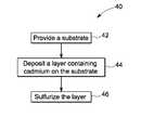
- FIG. 3illustrates a flow diagram of a method to make cadmium sulfide layer in accordance with some embodiments of the present invention
- FIG. 4illustrates a flow diagram of a method to make cadmium sulfide layer in accordance with an illustrative embodiment of the present invention
- FIG. 5illustrates a flow diagram of a method to make cadmium sulfide layer in accordance with another illustrative embodiment of the present invention
- FIG. 6illustrates a schematic cross sectional view of a chamber suitable for sputter deposition in accordance with some embodiments of the present invention.
- Approximating languagemay be applied to modify any quantitative representation that could permissibly vary without resulting in a change in the basic function to which it is related. Accordingly, a value modified by a term or terms, such as “about”, is not limited to the precise value specified. In some instances, the approximating language may correspond to the precision of an instrument for measuring the value.
- the terms “may” and “may be”indicate a possibility of an occurrence within a set of circumstances; a possession of a specified property, characteristic or function; and/or qualify another verb by expressing one or more of an ability, capability, or possibility associated with the qualified verb. Accordingly, usage of “may” and “may be” indicates that a modified term is apparently appropriate, capable, or suitable for an indicated capacity, function, or usage, while taking into account that in some circumstances the modified term may sometimes not be appropriate, capable, or suitable. For example, in some circumstances, an event or capacity can be expected, while in other circumstances the event or capacity cannot occur—this distinction is captured by the terms “may” and “may be”.
- transparentmeans that a material allows the passage of a substantial portion of incident solar radiation.
- the substantial portionmay be at least about 80% of the incident solar radiation.
- PVphotovoltaic
- CdTecadmium telluride
- CIGSCu(In,Ga,Al)(Se,S) 2
- Other examples of PV cellsmay include a copper-zinc-tin-sulfide (CZTS) PV cell and a metal sulfide PV cell.
- CZTScopper-zinc-tin-sulfide
- a photovoltaic cellgenerally includes a substrate, a transparent electrode, a CdS window layer, an absorber layer, and a base electrode.
- FIG. 1illustrates a CdTe PV cell 10 that includes a transparent substrate 12 .
- the substrate 12includes a transparent conductive layer 14 that forms the transparent electrode.
- the CdS window layer 16is deposited on the transparent conductive layer 14 followed by the absorber layer 18 .
- the transparent conductive layer 14(also referred to as TCO layer when the layer includes an oxide) is disposed on a surface of the substrate 12 .
- Suitable materials for the transparent conductive layer 14may include an oxide, sulfide, phosphide, telluride, or combinations thereof. These transparent conductive materials may be doped or undoped.
- the transparent conductive layer 14may include an oxide, such as titanium dioxide, silicon oxide, zinc oxide, tin oxide, aluminum doped zinc oxide, fluorine-doped tin oxide, cadmium stannate (cadmium tin oxide), or zinc stannate (zinc tin oxide).
- the transparent conductive layer 14includes one or more indium-containing oxides.
- suitable indium containing oxidesare indium tin oxide (ITO), Ga—In—Sn—O, Zn—In—Sn—O, Ga—In—O, Zn—In—O, and combinations thereof.
- Suitable phosphidesmay include indium phosphide, gallium phosphide, and the like.
- An optional secondary transparent conductive layer 15 with higher sheet resistance than that of the transparent conductive layer 14may be disposed over the transparent conductive layer 14 .
- This secondary transparent conductive layer 15is known as high-resistance transparent (HRT) layer or high-resistance transparent conductive layer.
- Undoped zinc stannate (ZnSnO 4 ), zinc oxide (ZnO), and tin oxide (SiO 2 )may be employed as the HRT layer.
- the HRT layerusually permits the use of a thinner CdS window layer in a photovoltaic cell than is feasible without the HRT layer, thereby increasing the quantum efficiency of the cell in the blue region.
- the HRT layermay also improve the cell efficiency by forming a barrier against diffusion of unwanted species from the substrate 12 and a front contact to the CdS window layer 16 .
- FIG. 2shows an illustrative embodiment of a CIGS PV cell or a copper-zinc-tin-sulfide (CZTS) PV cell.
- the cell 20includes a substrate 22 that may be non-transparent.
- a non-transparent layer 24is disposed on the substrate 22 to form the absorber layer and a CdS window layer 26 is deposited over the non-transparent layer 24 .
- a transparent conductive layer 28may be disposed on the window layer 26 .
- the non-transparent layer 24includes one or more elements selected from the group consisting of copper, silver, indium, gallium, aluminum, zinc, tin and selenium.
- the non-transparent layerincludes copper.
- a photoactive materialis typically used for forming an absorber layer.
- suitable photoactive materialsmay include cadmium telluride (CdTe), Cu(In,Ga,Al)(Se,S) 2 (CIGS) and copper-zinc-tin-sulfide (CZTS). In some instances, these materials may further be substituted with one or more additional elements.
- CdS thin filmsThere are a number of ways to deposit CdS thin films.
- One way of producing CdS filmsis by spraying a solution of a cadmium salt and a soluble sulfide. Cadmium sulfide is thus formed by a double decomposition reaction in situ on the substrate. See, for instance, U.S. Pat. No. 4,159,914.
- Another spraying techniqueinvolves chemical spray deposition of an oxide film of cadmium, followed by treatment of the oxide film with hydrogen sulfide, reactive therewith to produce cadmium sulfide. See, for instance, U.S. Pat. No. 4,242,374.
- the cadmium oxide filmis obtained by spray deposition and thermal decomposition of a soluble cadmium salt, such as cadmium nitrate, cadmium oxalate, or cadmium acetate. These processes are complicated, and difficult to control. A double decomposition condensation, or similar reaction of two chemicals in situ to produce one or several different chemicals, depends upon relative proportions of the chemicals, their concentrations, the reaction temperature and the reaction time.
- CdS thin filmsare produced by sputtering from a CdS target, which is an extremely expensive material.
- Sputteringis a well-known and widely used technique for efficient and large-scale coatings.
- sputtering from a CdS targetis slow and expensive in bill of material cost.
- Embodiments of the invention described hereinprovide an alternative method to address the noted shortcomings of the state of the art.
- the method of making a cadmium sulfide layerincludes steps in the sequence as illustrated in flow diagram 40 of FIG. 3 , according to one embodiment of the invention.
- Step 42provides a substrate.
- Substrate selectiondepends on desired application, for example type of PV cell.
- Suitable examples of substrate materialmay include, but are not limited to, glass, semiconductor, doped semiconductor, amorphous dielectrics, crystalline dielectrics, metal, polymer and combinations thereof.
- the substrateis a glass plate.
- the substrateis a flexible polyimide.
- the substrateincludes a metal.
- the substratein some embodiments, has a substantially planar surface.
- the surfacecan be smooth, although it may include a relatively minor degree (e.g., an RMS roughness that is less than about 1 micron, or more specifically less than about 300 nm) of texture, indentations, and various irregularities.
- the method 40further includes the step 44 of disposing a cadmium-containing layer on the substrate.
- the layerincludes cadmium metal.
- the cadmium-containing layeris deposited over the transparent conductive layer 14 , as shown in FIG. 1 and depicted in flow diagram of FIG. 4 . In these instances, if a HRT layer is employed, the cadmium-containing layer is deposited over the HRT layer 15 . In some other embodiments, the cadmium-containing layer is deposited over the non-transparent layer 24 as shown in FIG. 2 and depicted in flow diagram of FIG. 5 .
- Various thin-film deposition techniquescan be used to deposit the cadmium-containing layer, for example chemical bath deposition, sol-gel, electrochemical deposition, thermal evaporation, sputtering, and spraying.
- a vacuum deposition techniqueis used to attain a high quality film.
- Non-limiting examples of vacuum deposition techniqueinclude evaporation deposition, electron beam physical vapor deposition, sputter deposition, cathode arc deposition, or pulsed laser deposition.
- sputteringis a desirable deposition technique for the deposition of high quality films over large areas, in simple and controllable way.
- FIG. 6illustrates an example of a sputtering system 50 .
- Sputtering system 50typically includes a vacuum chamber 52 .
- a sputtering source 56is connected to a power source 54 and includes a sputter gun and a target (not shown) for sputtering operations.
- the power source 54may be a direct current (DC), a radiofrequency (RF) power, a bipolar pulsed direct current, a high power pulsed direct current or any combination thereof.
- the sputtering source 56is mounted on a support 58 extending into the vacuum chamber 52 .
- the targetincludes cadmium metal.
- the sputtering system 50utilizes an atmosphere of gas having heavy ions, such as argon.
- a substrate holder 60supports a substrate 62 , which is typically held in an orientation and at distance suitable for film growth.
- the substrate 62may be heated.
- the substrate 62is placed in the chamber 52 for about 10 to about 90 minutes, depending on desired thickness of the layer.
- the thickness of desired cadmium sulfide (CdS) layeris typically required to be minimized in a PV cell to achieve high efficiency.
- the thickness of the cadmium-containing layermay be between about 10 nanometers and about 200 nanometers depending in part on the sputtering time. In certain embodiments, the thickness of the layer ranges from about 50 nanometers to about 100 nanometers.
- the cadmium metalmay be deposited using an in-line system with multiple sputtering sources.
- the method 40further provides step 46 for sulfurization of the cadmium-containing layer.
- sulfurizationrefers to exposing the cadmium-containing layer in a sulfur-containing atmosphere to substantially transform the cadmium to cadmium sulfide.
- the sulfur-containing atmosphereincludes a sulfur-containing gas.
- Suitable examples of sulfur-containing gasinclude, but are not limited to, hydrogen sulfide, carbon disulfide, sulfur hexafluoride (SF 6 ), sulfur dichloride, alkane thiols, and thioethers.
- Other examplesmay include organometallic precursors, although these species may leave undesirable organic residues after the process.
- sulfurizationoccurs below a temperature at which the formed sulfide decomposes or sublimes.
- sulfurization of the cadmium-containing layeris carried out in a temperature range of about 100 degrees Celsius to about 1000 degrees Celsius. In certain instances, the sulfurization temperature ranges from about 200 degrees Celsius to about 500 degrees Celsius. Transformation of the cadmium-containing layer to cadmium sulfide layer depends in part on the thickness of the layer, the sulfurization time, and the temperature selected. In some embodiments, sulfurization of the cadmium-containing layer is carried out for a period ranging of about 2 minutes to about 5 hours, and in certain embodiments, about 5 minutes to about 30 minutes.
- the sulfurization time and sulfurization temperatureare selected to convert at least about 50% of the cadmium in the cadmium-containing layer to cadmium sulfide (CdS). In some embodiments, at least about 80% of cadmium, and in some embodiments, substantially all of the cadmium is converted to cadmium sulfide.
- the sulfurization of the cadmium-containing layermay be carried out inside the vacuum chamber after deposition of the layer, for example to avoid oxidization of cadmium.
- the sulfurization of the cadmium-containing layermay be accomplished outside the vacuum chamber, for example to avoid contamination of the vacuum chamber.
- the cadmium-containing layermay be shifted to another region or zone of the vacuum chamber after deposition to carry out sulfurization.
- the cadmium-containing layeris disposed on the non-transparent layer.
- the non-transparent layer and the cadmium-containing layerare both sulfurized at the same time to form the photoactive material layer and cadmium sulfide layer, respectively.
- a certain amount of oxygencan be incorporated in the cadmium-containing layer to form a CdS:O film after sulfurization.
- the oxygen contentis usually greater than about 1 atomic percent and less than about 50 atomic percent in the cadmium-containing layer.
- the oxygen contentmay vary between about 1 atomic percent and about 45 atomic percent, and more specifically, between about 2 atomic percent and about 20 atomic percent.
- the above-discussed methodadvantageously provides a relatively economic process to deposit a cadmium sulfide layer as compared to currently available methods.
- the methodis relatively economical with respect to both cost and time.
- Sputtering cadmium sulfide (CdS)is difficult and takes a long time due to slow growth rates, when compared with sputtering metallic cadmium.
- CdS targetsare relatively expensive compared to metallic cadmium targets. The present method thus saves time and materials cost compared to conventional deposition of CdS.
Landscapes
- Photovoltaic Devices (AREA)
- Chemically Coating (AREA)
- Physical Vapour Deposition (AREA)
Abstract
Description
Claims (20)
Priority Applications (4)
| Application Number | Priority Date | Filing Date | Title |
|---|---|---|---|
| US12/951,108US8119513B1 (en) | 2010-11-22 | 2010-11-22 | Method for making cadmium sulfide layer |
| MYPI2011005557AMY169831A (en) | 2010-11-22 | 2011-11-17 | Method for making cadmium sulfide layer |
| DE102011055618ADE102011055618A1 (en) | 2010-11-22 | 2011-11-22 | Process for producing a cadmium sulfide layer |
| CN201110461918.2ACN102544213B (en) | 2010-11-22 | 2011-11-22 | The method manufacturing cadmium sulfide layer |
Applications Claiming Priority (1)
| Application Number | Priority Date | Filing Date | Title |
|---|---|---|---|
| US12/951,108US8119513B1 (en) | 2010-11-22 | 2010-11-22 | Method for making cadmium sulfide layer |
Publications (1)
| Publication Number | Publication Date |
|---|---|
| US8119513B1true US8119513B1 (en) | 2012-02-21 |
Family
ID=45571993
Family Applications (1)
| Application Number | Title | Priority Date | Filing Date |
|---|---|---|---|
| US12/951,108Expired - Fee RelatedUS8119513B1 (en) | 2010-11-22 | 2010-11-22 | Method for making cadmium sulfide layer |
Country Status (4)
| Country | Link |
|---|---|
| US (1) | US8119513B1 (en) |
| CN (1) | CN102544213B (en) |
| DE (1) | DE102011055618A1 (en) |
| MY (1) | MY169831A (en) |
Cited By (1)
| Publication number | Priority date | Publication date | Assignee | Title |
|---|---|---|---|---|
| US20110315209A1 (en)* | 2010-06-29 | 2011-12-29 | Primestar Solar | Selectively deposited thin film devices and methods for forming selectively deposited thin films |
Families Citing this family (3)
| Publication number | Priority date | Publication date | Assignee | Title |
|---|---|---|---|---|
| US9007674B2 (en) | 2011-09-30 | 2015-04-14 | View, Inc. | Defect-mitigation layers in electrochromic devices |
| US20170038658A1 (en) | 2011-09-30 | 2017-02-09 | View, Inc. | Particle removal during fabrication of electrochromic devices |
| CN114706252A (en)* | 2014-04-22 | 2022-07-05 | 唯景公司 | Particle removal during fabrication of electrochromic devices |
Citations (20)
| Publication number | Priority date | Publication date | Assignee | Title |
|---|---|---|---|---|
| US4025339A (en)* | 1974-01-18 | 1977-05-24 | Coulter Information Systems, Inc. | Electrophotographic film, method of making the same and photoconductive coating used therewith |
| US4035819A (en) | 1973-10-19 | 1977-07-12 | Matsushita Electric Industrial Co., Ltd. | Method of making a zinc sulphide ceramic body and a zinc sulphide ceramic body made thereby |
| US4041140A (en) | 1974-07-16 | 1977-08-09 | Matsushita Electric Industrial Co., Ltd. | Method of making a sulphide ceramic body |
| US4178395A (en)* | 1977-11-30 | 1979-12-11 | Photon Power, Inc. | Methods for improving solar cell open circuit voltage |
| US4331707A (en)* | 1980-10-15 | 1982-05-25 | Exxon Research & Engineering Co. | Process for thin film deposition of cadmium sulfide |
| US4360542A (en)* | 1981-03-31 | 1982-11-23 | Argus Chemical Corporation | Process for the preparation of thin films of cadmium sulfide and precursor solutions of cadmium ammonia thiocyanate complex useful therein |
| US4612411A (en)* | 1985-06-04 | 1986-09-16 | Atlantic Richfield Company | Thin film solar cell with ZnO window layer |
| US4647711A (en)* | 1985-01-29 | 1987-03-03 | The Standard Oil Company | Stable front contact current collector for photovoltaic devices and method of making same |
| US5032374A (en) | 1987-10-22 | 1991-07-16 | Hughes Aircraft Company | Preparation of metal sulfides |
| US5202290A (en) | 1991-12-02 | 1993-04-13 | Martin Moskovits | Process for manufacture of quantum dot and quantum wire semiconductors |
| US5541118A (en)* | 1995-05-22 | 1996-07-30 | Midwest Research Institute | Process for producing cadmium sulfide on a cadmium telluride surface |
| US5674325A (en)* | 1995-06-07 | 1997-10-07 | Photon Energy, Inc. | Thin film photovoltaic device and process of manufacture |
| US5728231A (en) | 1995-05-15 | 1998-03-17 | Matsushita Electric Industrial Co., Ltd. | Precursor for semiconductor thin films and method for producing semiconductor thin films |
| US6303097B1 (en) | 1993-06-03 | 2001-10-16 | Merck Patent Gesellschaft Mit Beschrankter Haftung | Process for the preparation of metal sulphides |
| US20030011047A1 (en)* | 2001-05-08 | 2003-01-16 | Cunningham Daniel W. | Photovoltaic device |
| US20050186342A1 (en) | 2004-02-19 | 2005-08-25 | Nanosolar, Inc. | Formation of CIGS absorber layer materials using atomic layer deposition and high throughput surface treatment |
| US20060057766A1 (en)* | 2003-07-08 | 2006-03-16 | Quanxi Jia | Method for preparation of semiconductive films |
| US7017382B2 (en) | 2000-03-28 | 2006-03-28 | Honeywell International Inc. | Methods of forming aluminum-comprising physical vapor deposition targets; sputtered films; and target constructions |
| US7482059B2 (en) | 2004-05-10 | 2009-01-27 | Evident Technologies | Semiconductor nanocrystal complexes comprising a metal coating and methods of making same |
| US7704914B2 (en) | 2002-03-18 | 2010-04-27 | Nittetsu Mining Co., Ltd. | Photocatalyst and process for producing the same |
Family Cites Families (4)
| Publication number | Priority date | Publication date | Assignee | Title |
|---|---|---|---|---|
| DK126876A (en) | 1975-11-14 | 1977-05-15 | Photon Power Inc | PROCEDURE FOR MAKING A PHOTO ELEMENT |
| US4242374A (en) | 1979-04-19 | 1980-12-30 | Exxon Research & Engineering Co. | Process for thin film deposition of metal and mixed metal chalcogenides displaying semi-conductor properties |
| CN101452969B (en)* | 2008-12-29 | 2010-06-02 | 上海太阳能电池研究与发展中心 | Copper zincium tin sulfur compound semiconductor thin-film solar cell and manufacturing method |
| CN101882653B (en)* | 2010-06-29 | 2011-08-31 | 上海大学 | Preparation method of solar battery based on nano CdS (Cadmium Sulfide) film |
- 2010
- 2010-11-22USUS12/951,108patent/US8119513B1/ennot_activeExpired - Fee Related
- 2011
- 2011-11-17MYMYPI2011005557Apatent/MY169831A/enunknown
- 2011-11-22CNCN201110461918.2Apatent/CN102544213B/ennot_activeExpired - Fee Related
- 2011-11-22DEDE102011055618Apatent/DE102011055618A1/ennot_activeCeased
Patent Citations (21)
| Publication number | Priority date | Publication date | Assignee | Title |
|---|---|---|---|---|
| US4035819A (en) | 1973-10-19 | 1977-07-12 | Matsushita Electric Industrial Co., Ltd. | Method of making a zinc sulphide ceramic body and a zinc sulphide ceramic body made thereby |
| US4025339A (en)* | 1974-01-18 | 1977-05-24 | Coulter Information Systems, Inc. | Electrophotographic film, method of making the same and photoconductive coating used therewith |
| US4041140A (en) | 1974-07-16 | 1977-08-09 | Matsushita Electric Industrial Co., Ltd. | Method of making a sulphide ceramic body |
| US4178395A (en)* | 1977-11-30 | 1979-12-11 | Photon Power, Inc. | Methods for improving solar cell open circuit voltage |
| US4331707A (en)* | 1980-10-15 | 1982-05-25 | Exxon Research & Engineering Co. | Process for thin film deposition of cadmium sulfide |
| US4360542A (en)* | 1981-03-31 | 1982-11-23 | Argus Chemical Corporation | Process for the preparation of thin films of cadmium sulfide and precursor solutions of cadmium ammonia thiocyanate complex useful therein |
| US4647711A (en)* | 1985-01-29 | 1987-03-03 | The Standard Oil Company | Stable front contact current collector for photovoltaic devices and method of making same |
| US4612411A (en)* | 1985-06-04 | 1986-09-16 | Atlantic Richfield Company | Thin film solar cell with ZnO window layer |
| US5032374A (en) | 1987-10-22 | 1991-07-16 | Hughes Aircraft Company | Preparation of metal sulfides |
| US5202290A (en) | 1991-12-02 | 1993-04-13 | Martin Moskovits | Process for manufacture of quantum dot and quantum wire semiconductors |
| US6303097B1 (en) | 1993-06-03 | 2001-10-16 | Merck Patent Gesellschaft Mit Beschrankter Haftung | Process for the preparation of metal sulphides |
| US5728231A (en) | 1995-05-15 | 1998-03-17 | Matsushita Electric Industrial Co., Ltd. | Precursor for semiconductor thin films and method for producing semiconductor thin films |
| US5541118A (en)* | 1995-05-22 | 1996-07-30 | Midwest Research Institute | Process for producing cadmium sulfide on a cadmium telluride surface |
| US5868869A (en)* | 1995-06-07 | 1999-02-09 | Photon Energy, Inc. | Thin film photovoltaic device and process of manufacture |
| US5674325A (en)* | 1995-06-07 | 1997-10-07 | Photon Energy, Inc. | Thin film photovoltaic device and process of manufacture |
| US7017382B2 (en) | 2000-03-28 | 2006-03-28 | Honeywell International Inc. | Methods of forming aluminum-comprising physical vapor deposition targets; sputtered films; and target constructions |
| US20030011047A1 (en)* | 2001-05-08 | 2003-01-16 | Cunningham Daniel W. | Photovoltaic device |
| US7704914B2 (en) | 2002-03-18 | 2010-04-27 | Nittetsu Mining Co., Ltd. | Photocatalyst and process for producing the same |
| US20060057766A1 (en)* | 2003-07-08 | 2006-03-16 | Quanxi Jia | Method for preparation of semiconductive films |
| US20050186342A1 (en) | 2004-02-19 | 2005-08-25 | Nanosolar, Inc. | Formation of CIGS absorber layer materials using atomic layer deposition and high throughput surface treatment |
| US7482059B2 (en) | 2004-05-10 | 2009-01-27 | Evident Technologies | Semiconductor nanocrystal complexes comprising a metal coating and methods of making same |
Non-Patent Citations (4)
| Title |
|---|
| B. E. McCandless, A. Mondal, R. W. Birkmire, Galvanic deposition of cadmium sulfide thin films, Solar Energy Materials and Solar Cells, vol. 36, Issue 4, Apr. 1995, pp. 369-379, I.* |
| Jichun Fan, Tao Gao, Guowen Meng, Yewu Wang, Xiong Liu, Lide Zhang; "Synthesis of CdS nanowires by sulfurization", Materials Letters, Elsevier Science B.V., Dec. 2002, vol. 57, pp. 656-659. |
| K.S. Balakrishnan, A.C. Rastogi; "Structure and growth kinetics of electrodeposited Cds thin films for solar cell applications", Solar Energy Materials, Published by Elsevier B.V., Jun. 1990, vol. 20, Issues 5-6, pp. 417-434. |
| Xuanzhi Wu, High-efficiency polycrystalline CdTe thin-film solar cells, Solar Energy, vol. 77, Issue 6, Thin Film PV, Dec. 2004, pp. 803-814, ISSN 0038-092X.* |
Cited By (2)
| Publication number | Priority date | Publication date | Assignee | Title |
|---|---|---|---|---|
| US20110315209A1 (en)* | 2010-06-29 | 2011-12-29 | Primestar Solar | Selectively deposited thin film devices and methods for forming selectively deposited thin films |
| US8460765B2 (en)* | 2010-06-29 | 2013-06-11 | Primestar Solar, Inc. | Methods for forming selectively deposited thin films |
Also Published As
| Publication number | Publication date |
|---|---|
| MY169831A (en) | 2019-05-16 |
| CN102544213B (en) | 2017-03-01 |
| DE102011055618A1 (en) | 2012-05-24 |
| CN102544213A (en) | 2012-07-04 |
Similar Documents
| Publication | Publication Date | Title |
|---|---|---|
| Ravindiran et al. | Status review and the future prospects of CZTS based solar cell–A novel approach on the device structure and material modeling for CZTS based photovoltaic device | |
| US8390122B2 (en) | Sputtering targets including excess cadmium for forming a cadmium stannate layer | |
| US7943415B1 (en) | Methods of sputtering cadmium sulfide layers for use in cadmium telluride based thin film photovoltaic devices | |
| KR20150051181A (en) | PREPARATION METHOD OF CZTSSe-BASED THIN FILM SOLAR CELL AND CZTSSe-BASED THIN FILM SOLAR CELL PREPARED BY THE METHOD | |
| US8912037B2 (en) | Method for making photovoltaic devices using oxygenated semiconductor thin film layers | |
| JP2011129631A (en) | Method of manufacturing cis thin film solar cell | |
| US20130125962A1 (en) | Method for manufacturing light absorber layer of bismuth-doped ib-iiia-via compound and solar cell including the same | |
| US8053350B2 (en) | Methods of forming a conductive transparent oxide film layer for use in a cadmium telluride based thin film photovoltaic device | |
| US20120180858A1 (en) | Method for making semiconducting film and photovoltaic device | |
| US8119513B1 (en) | Method for making cadmium sulfide layer | |
| US20150027896A1 (en) | METHOD FOR PRODUCING Cu2ZnSnS4-xSex (0 LESS THAN-EQUAL TO X LESS THAN-EQUAL TO 4) THIN FILM BY ONE STEP ELECTRODEPOSITION IN ELECTROLYTIC BATH CONTAINING IONIC LIQUID | |
| AU2011202979B8 (en) | Apparatus and methods of forming a conductive transparent oxide film layer for use in a cadmium telluride based thin film photovoltaic device | |
| EP2702615B1 (en) | Method of preparing a solar cell | |
| US20120003784A1 (en) | Methods of forming a conductive transparent oxide film layer for use in a cadmium telluride based thin film photovoltaic device | |
| US9034686B2 (en) | Manufacturing methods for semiconductor devices | |
| TW201427054A (en) | Photoelectric conversion element, method of manufacturing the same, method of manufacturing buffer layer of photoelectric conversion element, and solar cell | |
| Pisarkiewicz et al. | Fabrication of thin film polycrystalline CIS photovoltaic heterostructure | |
| CN105679884A (en) | Preparation method of CZTS photovoltaic cell | |
| US20140134838A1 (en) | Methods of annealing a conductive transparent oxide film layer for use in a thin film photovoltaic device | |
| US20130133731A1 (en) | Cadmium doped tin oxide buffer layer for thin film photovoltaic devices and their methods of manufacture | |
| US20120067422A1 (en) | Photovoltaic device with a metal sulfide oxide window layer | |
| KR20150064930A (en) | Fabrication Method of Flexible CZTS Films and its application to Thin Film Solar Cells and Thin Film Solar Cells | |
| CN118186352B (en) | Buffer layer, copper indium gallium selenide thin film solar cell and preparation method thereof | |
| KR20150136721A (en) | Solar cell comprising high quality cigs absorber layer and method of fabricating the same | |
| US20130134037A1 (en) | Mixed targets for forming a cadmium doped tin oxide buffer layer in a thin film photovoltaic devices |
Legal Events
| Date | Code | Title | Description |
|---|---|---|---|
| AS | Assignment | Owner name:GENERAL ELECTRIC COMPANY, NEW YORK Free format text:ASSIGNMENT OF ASSIGNORS INTEREST;ASSIGNORS:DOREVAAR, BASTIAAN A.;FELDMAN-PEABODY, SCOTT;GOSSMAN, ROBERTQ D.;REEL/FRAME:025387/0221 Effective date:20101115 | |
| ZAAA | Notice of allowance and fees due | Free format text:ORIGINAL CODE: NOA | |
| ZAAB | Notice of allowance mailed | Free format text:ORIGINAL CODE: MN/=. | |
| FEPP | Fee payment procedure | Free format text:PAYOR NUMBER ASSIGNED (ORIGINAL EVENT CODE: ASPN); ENTITY STATUS OF PATENT OWNER: LARGE ENTITY | |
| STCF | Information on status: patent grant | Free format text:PATENTED CASE | |
| AS | Assignment | Owner name:FIRST SOLAR MALAYSIA SDN.BHD., MALAYSIA Free format text:ASSIGNMENT OF ASSIGNORS INTEREST;ASSIGNOR:GENERAL ELECTRIC COMPANY;REEL/FRAME:031581/0457 Effective date:20130805 | |
| AS | Assignment | Owner name:FIRST SOLAR, INC., ARIZONA Free format text:ASSIGNMENT OF ASSIGNORS INTEREST;ASSIGNOR:FIRST SOLAR MALAYSIA SDN. BHD.;REEL/FRAME:032045/0657 Effective date:20130805 | |
| AS | Assignment | Owner name:FIRST SOLAR, INC., ARIZONA Free format text:CORRECTIVE ASSIGNMENT TO CORRECT THE APPLICATION NUMBER FROM '13/301162' PREVIOUSLY RECORDED ON REEL 032045 FRAME 0657. ASSIGNOR(S) HEREBY CONFIRMS THE CORRECT APPLICATION NUMBER SHOULD BE '13/601162';ASSIGNOR:FIRST SOLAR MALAYSIA SDN. BHD.;REEL/FRAME:032239/0005 Effective date:20130805 | |
| FPAY | Fee payment | Year of fee payment:4 | |
| AS | Assignment | Owner name:JPMORGAN CHASE BANK, N.A., AS ADMINISTRATIVE AGENT, ILLINOIS Free format text:PATENT SECURITY AGREEMENT;ASSIGNOR:FIRST SOLAR, INC.;REEL/FRAME:043177/0581 Effective date:20170710 Owner name:JPMORGAN CHASE BANK, N.A., AS ADMINISTRATIVE AGENT Free format text:PATENT SECURITY AGREEMENT;ASSIGNOR:FIRST SOLAR, INC.;REEL/FRAME:043177/0581 Effective date:20170710 | |
| MAFP | Maintenance fee payment | Free format text:PAYMENT OF MAINTENANCE FEE, 8TH YEAR, LARGE ENTITY (ORIGINAL EVENT CODE: M1552); ENTITY STATUS OF PATENT OWNER: LARGE ENTITY Year of fee payment:8 | |
| AS | Assignment | Owner name:FIRST SOLAR, INC., ARIZONA Free format text:TERMINATION AND RELEASE OF SECURITY INTEREST IN PATENT RIGHTS;ASSIGNOR:JPMORGAN CHASE BANK, N.A.;REEL/FRAME:058132/0566 Effective date:20210825 | |
| FEPP | Fee payment procedure | Free format text:MAINTENANCE FEE REMINDER MAILED (ORIGINAL EVENT CODE: REM.); ENTITY STATUS OF PATENT OWNER: LARGE ENTITY | |
| LAPS | Lapse for failure to pay maintenance fees | Free format text:PATENT EXPIRED FOR FAILURE TO PAY MAINTENANCE FEES (ORIGINAL EVENT CODE: EXP.); ENTITY STATUS OF PATENT OWNER: LARGE ENTITY | |
| STCH | Information on status: patent discontinuation | Free format text:PATENT EXPIRED DUE TO NONPAYMENT OF MAINTENANCE FEES UNDER 37 CFR 1.362 | |
| FP | Lapsed due to failure to pay maintenance fee | Effective date:20240221 |