US8119472B2 - Silicon device on Si:C SOI and SiGe and method of manufacture - Google Patents
Silicon device on Si:C SOI and SiGe and method of manufactureDownload PDFInfo
- Publication number
- US8119472B2 US8119472B2US11/757,883US75788307AUS8119472B2US 8119472 B2US8119472 B2US 8119472B2US 75788307 AUS75788307 AUS 75788307AUS 8119472 B2US8119472 B2US 8119472B2
- Authority
- US
- United States
- Prior art keywords
- island
- layer
- substrate
- region
- sti
- Prior art date
- Legal status (The legal status is an assumption and is not a legal conclusion. Google has not performed a legal analysis and makes no representation as to the accuracy of the status listed.)
- Active, expires
Links
- 238000000034methodMethods0.000titleclaimsabstractdescription60
- 238000004519manufacturing processMethods0.000titleclaimsabstractdescription24
- 229910000577Silicon-germaniumInorganic materials0.000titleclaimsdescription44
- 229910052710siliconInorganic materials0.000titleclaimsdescription16
- XUIMIQQOPSSXEZ-UHFFFAOYSA-NSiliconChemical compound[Si]XUIMIQQOPSSXEZ-UHFFFAOYSA-N0.000titledescription8
- 239000010703siliconSubstances0.000titledescription8
- 239000000463materialSubstances0.000claimsabstractdescription106
- 239000000758substrateSubstances0.000claimsabstractdescription51
- 238000002955isolationMethods0.000claimsabstractdescription23
- 239000004065semiconductorSubstances0.000claimsabstractdescription17
- 238000000137annealingMethods0.000claimsdescription16
- 238000000151depositionMethods0.000claimsdescription9
- 230000002040relaxant effectEffects0.000claims1
- 239000013078crystalSubstances0.000description16
- 235000012431wafersNutrition0.000description11
- 238000001289rapid thermal chemical vapour depositionMethods0.000description10
- 238000000038ultrahigh vacuum chemical vapour depositionMethods0.000description10
- VYPSYNLAJGMNEJ-UHFFFAOYSA-NSilicium dioxideChemical compoundO=[Si]=OVYPSYNLAJGMNEJ-UHFFFAOYSA-N0.000description8
- 238000007796conventional methodMethods0.000description6
- 230000008021depositionEffects0.000description6
- 150000004767nitridesChemical class0.000description6
- 238000001020plasma etchingMethods0.000description6
- 238000012545processingMethods0.000description6
- 238000006243chemical reactionMethods0.000description5
- 238000005137deposition processMethods0.000description5
- 238000002156mixingMethods0.000description5
- 238000005229chemical vapour depositionMethods0.000description4
- 229910052681coesiteInorganic materials0.000description4
- 229910052906cristobaliteInorganic materials0.000description4
- 230000007547defectEffects0.000description4
- -1e.g.Substances0.000description4
- 239000010408filmSubstances0.000description4
- 239000012212insulatorSubstances0.000description4
- 230000003647oxidationEffects0.000description4
- 238000007254oxidation reactionMethods0.000description4
- 239000000377silicon dioxideSubstances0.000description4
- 229910052682stishoviteInorganic materials0.000description4
- 229910052905tridymiteInorganic materials0.000description4
- 230000015572biosynthetic processEffects0.000description3
- 239000011248coating agentSubstances0.000description3
- 238000000576coating methodMethods0.000description3
- 238000000623plasma-assisted chemical vapour depositionMethods0.000description3
- 238000013459approachMethods0.000description2
- QVGXLLKOCUKJST-UHFFFAOYSA-Natomic oxygenChemical compound[O]QVGXLLKOCUKJST-UHFFFAOYSA-N0.000description2
- 238000001312dry etchingMethods0.000description2
- 230000005669field effectEffects0.000description2
- 238000005468ion implantationMethods0.000description2
- 238000001459lithographyMethods0.000description2
- TWNQGVIAIRXVLR-UHFFFAOYSA-Noxo(oxoalumanyloxy)alumaneChemical compoundO=[Al]O[Al]=OTWNQGVIAIRXVLR-UHFFFAOYSA-N0.000description2
- 229910052760oxygenInorganic materials0.000description2
- 239000001301oxygenSubstances0.000description2
- RVTZCBVAJQQJTK-UHFFFAOYSA-Noxygen(2-);zirconium(4+)Chemical compound[O-2].[O-2].[Zr+4]RVTZCBVAJQQJTK-UHFFFAOYSA-N0.000description2
- 238000000059patterningMethods0.000description2
- 125000006850spacer groupChemical group0.000description2
- 238000010561standard procedureMethods0.000description2
- 239000000126substanceSubstances0.000description2
- 239000010409thin filmSubstances0.000description2
- 238000001039wet etchingMethods0.000description2
- 229910001928zirconium oxideInorganic materials0.000description2
- 230000009286beneficial effectEffects0.000description1
- 230000006835compressionEffects0.000description1
- 238000007906compressionMethods0.000description1
- 239000004020conductorSubstances0.000description1
- 230000001627detrimental effectEffects0.000description1
- 230000003292diminished effectEffects0.000description1
- 238000005530etchingMethods0.000description1
- 238000001704evaporationMethods0.000description1
- 230000008020evaporationEffects0.000description1
- 239000011521glassSubstances0.000description1
- 238000012986modificationMethods0.000description1
- 230000004048modificationEffects0.000description1
- 238000001451molecular beam epitaxyMethods0.000description1
- 229910021421monocrystalline siliconInorganic materials0.000description1
- 230000035945sensitivityEffects0.000description1
- 238000000926separation methodMethods0.000description1
- 230000003746surface roughnessEffects0.000description1
- 239000011345viscous materialSubstances0.000description1
Images


Classifications
- H—ELECTRICITY
- H10—SEMICONDUCTOR DEVICES; ELECTRIC SOLID-STATE DEVICES NOT OTHERWISE PROVIDED FOR
- H10D—INORGANIC ELECTRIC SEMICONDUCTOR DEVICES
- H10D84/00—Integrated devices formed in or on semiconductor substrates that comprise only semiconducting layers, e.g. on Si wafers or on GaAs-on-Si wafers
- H10D84/01—Manufacture or treatment
- H10D84/0123—Integrating together multiple components covered by H10D12/00 or H10D30/00, e.g. integrating multiple IGBTs
- H10D84/0126—Integrating together multiple components covered by H10D12/00 or H10D30/00, e.g. integrating multiple IGBTs the components including insulated gates, e.g. IGFETs
- H10D84/0165—Integrating together multiple components covered by H10D12/00 or H10D30/00, e.g. integrating multiple IGBTs the components including insulated gates, e.g. IGFETs the components including complementary IGFETs, e.g. CMOS devices
- H10D84/0167—Manufacturing their channels
- H—ELECTRICITY
- H10—SEMICONDUCTOR DEVICES; ELECTRIC SOLID-STATE DEVICES NOT OTHERWISE PROVIDED FOR
- H10D—INORGANIC ELECTRIC SEMICONDUCTOR DEVICES
- H10D10/00—Bipolar junction transistors [BJT]
- H10D10/80—Heterojunction BJTs
- H10D10/821—Vertical heterojunction BJTs
- H10D10/891—Vertical heterojunction BJTs comprising lattice-mismatched active layers, e.g. SiGe strained-layer transistors
- H—ELECTRICITY
- H10—SEMICONDUCTOR DEVICES; ELECTRIC SOLID-STATE DEVICES NOT OTHERWISE PROVIDED FOR
- H10D—INORGANIC ELECTRIC SEMICONDUCTOR DEVICES
- H10D30/00—Field-effect transistors [FET]
- H10D30/01—Manufacture or treatment
- H10D30/021—Manufacture or treatment of FETs having insulated gates [IGFET]
- H10D30/027—Manufacture or treatment of FETs having insulated gates [IGFET] of lateral single-gate IGFETs
- H10D30/0278—Manufacture or treatment of FETs having insulated gates [IGFET] of lateral single-gate IGFETs forming single crystalline channels on wafers after forming insulating device isolations
- H—ELECTRICITY
- H10—SEMICONDUCTOR DEVICES; ELECTRIC SOLID-STATE DEVICES NOT OTHERWISE PROVIDED FOR
- H10D—INORGANIC ELECTRIC SEMICONDUCTOR DEVICES
- H10D30/00—Field-effect transistors [FET]
- H10D30/60—Insulated-gate field-effect transistors [IGFET]
- H10D30/751—Insulated-gate field-effect transistors [IGFET] having composition variations in the channel regions
- H—ELECTRICITY
- H10—SEMICONDUCTOR DEVICES; ELECTRIC SOLID-STATE DEVICES NOT OTHERWISE PROVIDED FOR
- H10D—INORGANIC ELECTRIC SEMICONDUCTOR DEVICES
- H10D30/00—Field-effect transistors [FET]
- H10D30/60—Insulated-gate field-effect transistors [IGFET]
- H10D30/791—Arrangements for exerting mechanical stress on the crystal lattice of the channel regions
- H10D30/792—Arrangements for exerting mechanical stress on the crystal lattice of the channel regions comprising applied insulating layers, e.g. stress liners
- H—ELECTRICITY
- H10—SEMICONDUCTOR DEVICES; ELECTRIC SOLID-STATE DEVICES NOT OTHERWISE PROVIDED FOR
- H10D—INORGANIC ELECTRIC SEMICONDUCTOR DEVICES
- H10D30/00—Field-effect transistors [FET]
- H10D30/60—Insulated-gate field-effect transistors [IGFET]
- H10D30/791—Arrangements for exerting mechanical stress on the crystal lattice of the channel regions
- H10D30/795—Arrangements for exerting mechanical stress on the crystal lattice of the channel regions being in lateral device isolation regions, e.g. STI
- H—ELECTRICITY
- H10—SEMICONDUCTOR DEVICES; ELECTRIC SOLID-STATE DEVICES NOT OTHERWISE PROVIDED FOR
- H10D—INORGANIC ELECTRIC SEMICONDUCTOR DEVICES
- H10D30/00—Field-effect transistors [FET]
- H10D30/60—Insulated-gate field-effect transistors [IGFET]
- H10D30/791—Arrangements for exerting mechanical stress on the crystal lattice of the channel regions
- H10D30/798—Arrangements for exerting mechanical stress on the crystal lattice of the channel regions being provided in or under the channel regions
- H—ELECTRICITY
- H10—SEMICONDUCTOR DEVICES; ELECTRIC SOLID-STATE DEVICES NOT OTHERWISE PROVIDED FOR
- H10D—INORGANIC ELECTRIC SEMICONDUCTOR DEVICES
- H10D30/00—Field-effect transistors [FET]
- H10D30/80—FETs having rectifying junction gate electrodes
- H10D30/83—FETs having PN junction gate electrodes
- H10D30/832—Thin-film junction FETs [JFET]
- H—ELECTRICITY
- H10—SEMICONDUCTOR DEVICES; ELECTRIC SOLID-STATE DEVICES NOT OTHERWISE PROVIDED FOR
- H10D—INORGANIC ELECTRIC SEMICONDUCTOR DEVICES
- H10D62/00—Semiconductor bodies, or regions thereof, of devices having potential barriers
- H10D62/10—Shapes, relative sizes or dispositions of the regions of the semiconductor bodies; Shapes of the semiconductor bodies
- H10D62/113—Isolations within a component, i.e. internal isolations
- H10D62/115—Dielectric isolations, e.g. air gaps
- H—ELECTRICITY
- H10—SEMICONDUCTOR DEVICES; ELECTRIC SOLID-STATE DEVICES NOT OTHERWISE PROVIDED FOR
- H10D—INORGANIC ELECTRIC SEMICONDUCTOR DEVICES
- H10D62/00—Semiconductor bodies, or regions thereof, of devices having potential barriers
- H10D62/10—Shapes, relative sizes or dispositions of the regions of the semiconductor bodies; Shapes of the semiconductor bodies
- H10D62/17—Semiconductor regions connected to electrodes not carrying current to be rectified, amplified or switched, e.g. channel regions
- H10D62/393—Body regions of DMOS transistors or IGBTs
- H—ELECTRICITY
- H10—SEMICONDUCTOR DEVICES; ELECTRIC SOLID-STATE DEVICES NOT OTHERWISE PROVIDED FOR
- H10D—INORGANIC ELECTRIC SEMICONDUCTOR DEVICES
- H10D62/00—Semiconductor bodies, or regions thereof, of devices having potential barriers
- H10D62/80—Semiconductor bodies, or regions thereof, of devices having potential barriers characterised by the materials
- H10D62/83—Semiconductor bodies, or regions thereof, of devices having potential barriers characterised by the materials being Group IV materials, e.g. B-doped Si or undoped Ge
- H10D62/832—Semiconductor bodies, or regions thereof, of devices having potential barriers characterised by the materials being Group IV materials, e.g. B-doped Si or undoped Ge being Group IV materials comprising two or more elements, e.g. SiGe
- H10D62/8325—Silicon carbide
- H—ELECTRICITY
- H10—SEMICONDUCTOR DEVICES; ELECTRIC SOLID-STATE DEVICES NOT OTHERWISE PROVIDED FOR
- H10D—INORGANIC ELECTRIC SEMICONDUCTOR DEVICES
- H10D84/00—Integrated devices formed in or on semiconductor substrates that comprise only semiconducting layers, e.g. on Si wafers or on GaAs-on-Si wafers
- H10D84/01—Manufacture or treatment
- H10D84/0123—Integrating together multiple components covered by H10D12/00 or H10D30/00, e.g. integrating multiple IGBTs
- H10D84/0126—Integrating together multiple components covered by H10D12/00 or H10D30/00, e.g. integrating multiple IGBTs the components including insulated gates, e.g. IGFETs
- H10D84/0128—Manufacturing their channels
- H—ELECTRICITY
- H10—SEMICONDUCTOR DEVICES; ELECTRIC SOLID-STATE DEVICES NOT OTHERWISE PROVIDED FOR
- H10D—INORGANIC ELECTRIC SEMICONDUCTOR DEVICES
- H10D84/00—Integrated devices formed in or on semiconductor substrates that comprise only semiconducting layers, e.g. on Si wafers or on GaAs-on-Si wafers
- H10D84/01—Manufacture or treatment
- H10D84/02—Manufacture or treatment characterised by using material-based technologies
- H10D84/03—Manufacture or treatment characterised by using material-based technologies using Group IV technology, e.g. silicon technology or silicon-carbide [SiC] technology
- H10D84/035—Manufacture or treatment characterised by using material-based technologies using Group IV technology, e.g. silicon technology or silicon-carbide [SiC] technology using silicon carbide [SiC] technology
- H—ELECTRICITY
- H10—SEMICONDUCTOR DEVICES; ELECTRIC SOLID-STATE DEVICES NOT OTHERWISE PROVIDED FOR
- H10D—INORGANIC ELECTRIC SEMICONDUCTOR DEVICES
- H10D84/00—Integrated devices formed in or on semiconductor substrates that comprise only semiconducting layers, e.g. on Si wafers or on GaAs-on-Si wafers
- H10D84/01—Manufacture or treatment
- H10D84/02—Manufacture or treatment characterised by using material-based technologies
- H10D84/03—Manufacture or treatment characterised by using material-based technologies using Group IV technology, e.g. silicon technology or silicon-carbide [SiC] technology
- H10D84/038—Manufacture or treatment characterised by using material-based technologies using Group IV technology, e.g. silicon technology or silicon-carbide [SiC] technology using silicon technology, e.g. SiGe
- H—ELECTRICITY
- H10—SEMICONDUCTOR DEVICES; ELECTRIC SOLID-STATE DEVICES NOT OTHERWISE PROVIDED FOR
- H10D—INORGANIC ELECTRIC SEMICONDUCTOR DEVICES
- H10D86/00—Integrated devices formed in or on insulating or conducting substrates, e.g. formed in silicon-on-insulator [SOI] substrates or on stainless steel or glass substrates
- H10D86/01—Manufacture or treatment
- H—ELECTRICITY
- H10—SEMICONDUCTOR DEVICES; ELECTRIC SOLID-STATE DEVICES NOT OTHERWISE PROVIDED FOR
- H10D—INORGANIC ELECTRIC SEMICONDUCTOR DEVICES
- H10D86/00—Integrated devices formed in or on insulating or conducting substrates, e.g. formed in silicon-on-insulator [SOI] substrates or on stainless steel or glass substrates
- H10D86/201—Integrated devices formed in or on insulating or conducting substrates, e.g. formed in silicon-on-insulator [SOI] substrates or on stainless steel or glass substrates the substrates comprising an insulating layer on a semiconductor body, e.g. SOI
Definitions
- the inventiongenerally relates to a semiconductor device and method of manufacture and, more particularly, to a semiconductor device and method of manufacture which imposes tensile and compressive stresses in the device during device fabrication.
- n-type devicese.g., nFETs
- pFETsp-type devices
- the stress componentsshould be engineered and applied differently for nFETs and pFETs. That is, because the type of stress which is beneficial for the performance of an nFET is generally disadvantageous for the performance of the pFET. More particularly, when a device is in tension (e.g., in the direction of current flow in a planar device), the performance characteristics of the nFET are enhanced while the performance characteristics of the pFET are diminished. To selectively create tensile stress in an nFET and compressive stress in a pFET, distinctive processes and different combinations of materials are used.
- the isolation region for the nFET devicecontains a first isolation material which applies a first type of mechanical stress on the nFET device in a longitudinal direction (e.g., parallel to the direction of current flow) and in a transverse direction (e.g., perpendicular to the direction of current flow).
- a first isolation region and a second isolation regionare provided for the pFET and each of the isolation regions of the pFET device applies a unique mechanical stress on the pFET device in the transverse and longitudinal directions.
- liners on gate sidewallshave been proposed to selectively induce the appropriate stresses in the channels of the FET devices (see, Ootsuka et al., IEDM 2000, p. 575, for example).
- the appropriate stressis applied closer to the device than the stress applied as a result of the trench isolation fill technique.
- nFET and pFET device performanceusing tensile and compressive stresses, respectively, which include modulating spacer intrinsic stresses and STI (shallow trench isolation) material changes individually for two MOSFETs using masks.
- Tensilely strained Si on relaxed SiGehas also been proposed as a means to apply this stress.
- the tensilely strained Si on relaxed SiGecan apply only biaxial tensile stress on the Si cap as used in stack form. This constrains the regime of Ge % that is useful because of the nature of pFET sensitivity to stress.
- the nFET performancemonotonically improves with biaxial tension; however, the pFET is degraded with biaxial tension until about 3 GPa at which point it begins to improve.
- the Ge %In order to improve both the pFET and nFET simultaneously, the Ge % needs to be high, approximately greater than 25-30% (or equivalent to approximately greater than 3-4 GPa in stress). This level of Ge % is difficult to implement into processes and is not very manufacturable with major issues including surface roughness, process complexity, defect and yield control, to name but a few. Given that a high Ge % is hard to use for the pFET (since it would be detrimental because of the relatively low levels of tension), other methods must be devised to improve the device performance.
- Si:Cis know to grow epitaxially on Si where it is inherently tensile.
- a 1% C content in the Si:C/Si material stackcan cause tensile stress levels in the Si:C on the order of 500 MPa.
- about 6%is needed to cause a 500 MPa compression.
- This 1% level of Ccan be incorporated into Si during epitaxial growth as shown in Ernst et al., VLSI Symp., 2002, p. 92.
- the Si/Si:C/Siis in a layered channel for nFETs.
- the Si:C part of the structureis not relaxed. Instead, in Ernst, an unrelaxed Si:C is used as part of the channel, itself, with a very thin Si cap. The problem with this approach is that the mobility is not enhanced, but retarded, depending on the C content, from scattering.
- a method of manufacturing a structureincludes forming a substrate and shallow trench isolation in the substrate with a first material. A second material over a pFET region and an nFET region is formed, and is then thermally annealed into the substrate to form a first island and a second island of mixed material. A Si layer is grown on the first island in a first region. The Si layer is strained.
- the method of manufacturingincludes forming a substrate and shallow trench isolation of high temperature stable amorphous material, preferably oxide, in the substrate.
- the methodfurther includes thermally annealing at least one material into the substrate to form a first island and a second island of mixed material and growing a Si layer on at least the first island.
- the Si layeris strained.
- a semiconductor structurein another aspect of the invention, includes a substrate and a relaxed shallow trench isolation of high temperature stable amorphous material, preferably oxide, formed in the substrate.
- a first island of thermally annealed mixed materialis formed in the substrate at a pFET region and a second island of thermally annealed mixed material is formed in the substrate at an nFET region.
- a strained Si layeris formed on at least one of the first island and the second island.
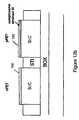
- FIGS. 1 through 6represent a fabrication process to form an intermediate structure in accordance with the invention
- FIGS. 7 through 11represent a fabrication process to form an intermediate structure in accordance with another aspect of the invention.
- FIGS. 12 a and 12 bare representative structures of the invention.
- This inventionis directed to a semiconductor device and method of manufacture which provides desired stresses in the nFET channel and the pFET channel of CMOS devices for improved device performance.
- a SiGe islandis obtained through thermally mixing deposited Ge material into an SOI thin film.
- a Si:C islandis obtained through thermally mixing deposited Si:C or C into the Si or SOI thin film.
- the required Ge %is not large and thus does not cause defect issues.
- relaxation of SiGe and/or Si:C islands in the channels of the pFET and nFET, respectivelycan be achieved by the invention to thus provide improved performance as compared to blanket (SiGe or Si:C) substrates. This is because, in the implementations of the invention, a high temperature thermal mixing step, for example, is provided such that shallow trench isolation (STI) can relax and facilitate the relaxation of the SiGe and Si:C islands.
- STIshallow trench isolation
- the methodsyield a unique substrate with small crystal islands which have a relaxed but different crystal structure.
- the nontrivial element of such structureis the use of high temperature stable amorphous material, e.g., SiO 2 , between the islands and the crystal on insulator structure.
- the unique structure with different (crystal) islandsallows for the placement of differently strained layers of optionally different crystals.
- the differently strained layersare tensile and compressive Si layers.
- the different layersare a tensile Si layer and SiGe layer or a compressive Si layer and Si:C layer.
- the inventionhas a seminal and important contribution to the art of making substrates with islands on insulator with multiple crystal lattice constants.
- a first island(crystal 1 ) has a lattice constant a ⁇ aSi and the second island (crystal 2 ) has a lattice constant a ⁇ aSi.
- a Si epitaxial layer of the inventioncan be selectively grown, which will strain tensilely and compressively on SiGe and Si:C, respectively. This particular application is suitable, for example, in strained planar nFETs and pFETs.
- silicon on glass (SOI) wafermay be fabricated using the SIMOX (Separation by IMplanted OXygen) process, which employs high dose ion implantation of oxygen and high temperature annealing to form a BOX layer in a bulk wafer.
- SIMOXSeparatation by IMplanted OXygen
- the wafercan be fabricated by bonding a device quality silicon wafer to another silicon wafer (the substrate layer) that has an oxide layer on its surface.
- the pairis then split apart, using a process that leaves a thin (relative to the thickness of the starting wafer), device-quality layer of single crystal silicon on top of the oxide layer (which has now become the BOX) on the substrate layer.
- the SOI wafermay also be formed using other processes.
- an Si layer 20is formed and patterned to form shallow trench isolation (STI) 25 using standard techniques of pad oxidation, pad nitride deposition, lithography based patterning, reactive ion etching (RIE) of the stack consisting of nitride, oxide, and silicon down to the buried oxide, edge oxidation, liner deposition, fill deposition, and chemical mechanical polish.
- STIshallow trench isolation
- RIEreactive ion etching
- the STI formation processis well known in the art.
- high temperature stable amorphous materiale.g., SiO 2 , is used for the STI.
- an epitaxial Ge material (layer) 30is deposited over the surface of the structure using conventional techniques such as chemical vapor deposition methods.
- ultrahigh vacuum chemical vapor depositionUHVCVD
- RTCVDrapid thermal chemical vapor deposition
- LPCVDlimited reaction processing CVD
- MBEmolecular beam epitaxy
- the thickness of the Ge materialmay range from 5 to 50 nanometers, or other dimension depending on the thickness of the underlying Si layer which may, for example, range from 30 to 100 nanometers.
- nFET hard mask 35is provided on a portion of the Ge layer 30 (e.g., at locations of a yet to be formed nFET device).
- the nFET hard mask 35may be a nitride hard mask formed using a conventional deposition process such as spin-on coating, CVD, plasma-assisted CVD, ultrahigh vacuum chemical vapor deposition (UHVCVD), rapid thermal chemical vapor deposition (RTCVD), limited reaction processing CVD (LRPCVD) and other like deposition processes.
- the exposed Ge layer 30is etched and the nFET mask 35 is stripped using techniques known in the art.
- the Ge layer 30may be selectively etched using RIE, wet or dry etching.
- a Si:C material 40(or optionally C) is deposited on the structure, including over the epitaxially deposited Ge material 35 .
- ultrahigh vacuum chemical vapor depositionUHVCVD
- UHVCVDultrahigh vacuum chemical vapor deposition
- Other conventional techniquesinclude rapid thermal chemical vapor deposition (RTCVD), limited reaction processing CVD (LRPCVD) and other like processes.
- RTCVDrapid thermal chemical vapor deposition
- LPCVDlimited reaction processing CVD
- the thickness of the Si:C or C materialmay range from 5 to 50 nanometers, or other dimension depending on the thickness of the underlying Si layer which may, for example, range from 30 to 100 nanometers. In another aspect, when using C, the thickness may range from 1 to 30 nanometers.
- a pFET hard mask 45is provided on a portion of the Si:C material 40 at locations of the yet to be formed pFET.
- the pFET hard mask 45may be a nitride hard mask formed using a conventional deposition process such as spin-on coating, CVD, plasma-assisted CVD, ultrahigh vacuum chemical vapor deposition (UHVCVD), rapid thermal chemical vapor deposition (RTCVD), limited reaction processing CVD (LRPCVD) and other like deposition processes.
- the exposed Si:C layer 40is then etched and the pFET mask 45 is stripped using techniques known in the art.
- the Si:C and pFETmay be etched using standard etching techniques such as, for example, RIE, wet or dry etching and the like.
- the structurethen undergoes a thermal annealing process.
- the deposited Ge material 30is mixed into the underlying SOI film to form an island 50 of substantially SiGe material.
- the deposited Si:C or optional C materialis mixed into the underlying SOI film forming an island 55 of substantially Si:C material.
- the thermal annealing processtakes place, for example, at about 1200° C. to 1350° C. between 1 hour and 10 hours, with one implementation at 1200° C. for approximately 5 hours.
- the required Ge %is not large (e.g., less than 25% and in one implementation 10 to 20%) for the nFET and thus does not cause defect issues.
- the STI 25can relax and facilitate the relaxation of the SiGe island 50 and Si:C island 55 . This is due, in part, because the STI comprises oxide material, which is a viscous material at the high temperature, e.g., becomes a low viscosity material at high temperature.
- the SiGe island 50 and the Si:C island 55have different relaxed crystal lattice (different dimensions between the atoms) which yield a unique substrate with small crystal islands.
- the relaxation of the SiGe island 50 and the Si:C island 55provides improved performance as compared to blanket (SiGe or Si:C) substrates.
- high temperature stable amorphous materiale.g., SiO 2
- SiO 2high temperature stable amorphous material
- a Si epitaxial layer 60is selectively grown on the SiGe island 50 and the Si:C island 55 by known processes.
- the selectively grown Si epitaxial layer 60will strain tensilely and compressively on the SiGe island and the Si:C island, respectively.
- the Si layer 60may range in thickness, for example, between 5 and 20 nanometers. As with all dimensions and the like, it is contemplated that other dimensions, temperatures, etc. may be used with the invention depending on, for example, the thickness of the underlying substrate.
- the SiGe island 50has a lattice constant a ⁇ aSi and the Si:C island 55 has a lattice constant a ⁇ aSi. That is, standing alone, the Si normally has a lower lattice constant than the SiGe layer; namely, the lattice constant of the Si material does not match the lattice constant of the SiGe layer.
- the lattice structure of the Si layerwill tend to match the lattice structure of the SiGe island.
- the Si layeris placed under a tensile stress. This area will act as a strained channel for the nFET.
- the Ge content of the SiGe layermay be less than 25% in ratio to the Si content.
- the lattice constant of the Si materialdoes not match the lattice constant of the Si:C.
- the lattice structure of the Si layerwill tend to match the lattice structure of the Si:C.
- the Si layeris placed under a compressive stress. That is, similar to the occurrence with the SiGe, the surrounding areas of the Si:C island will try to obtain an equilibrium state thus resulting in a compressive stress of an epitaxial Si layer formed on the Si:C island. This area will act as a strained channel for the pFET.
- the C contentmay be from about up to 4% in ratio to the Si content.
- FIGS. 7-11show another aspect of the invention.
- a silicon wafersuch as SOI is shown.
- the SOImay be fabricated using the SIMOX process or other well known processes.
- An Si layer 20is patterned to form shallow trench isolation (STI) 25 using standard techniques of pad oxidation, pad nitride deposition, lithography based patterning, reactive ion etching (RIE) of the stack consisting of nitride, oxide, and silicon down to the buried oxide, edge oxidation, liner deposition, fill deposition, and chemical mechanical polish.
- STIshallow trench isolation
- the STI formation processis well known in the art.
- a pFET mask 40is provided on a portion of the structure at locations of the yet to be formed pFET.
- the pFET hard maskmay be deposited using convention techniques such as chemical vapor deposition methods.
- such techniquesmay include spin-on coating, CVD, plasma-assisted CVD, evaporation ultrahigh vacuum chemical vapor deposition (UHVCVD), rapid thermal chemical vapor deposition (RTCVD), limited reaction processing CVD (LRPCVD) and other like deposition processes.
- An epitaxial Ge layer 30is selectively grown over the exposed surface of the yet to be formed nFET using conventional techniques.
- the thickness of the Ge materialmay range from 5 to 50 nanometers, or other dimension depending on the thickness of the underlying Si layer which may, for example, range from 30 to 100 nanometers.
- the hard mask 45is stripped using well known processes, as discussed above.
- an nFET mask 35is provided on a portion of the structure at locations of the yet to be formed nFET.
- the nFET hard maskmay be deposited using conventional techniques such as chemical vapor deposition methods as discussed throughout and which should be known to those of ordinary skill.
- An Si:C layer 40is selectively grown over the exposed surface of the structure at the yet to be formed pFET using conventional techniques such as chemical vapor deposition method, as discussed above.
- the thickness of the Si:C materialmay range from 5 to 50 nanometers, or other dimension depending on the thickness of the underlying Si layer which may, for example, range from 30 to 100 nanometers.
- the Cmay even be thinner ranging from 1 to 50 nanometers.
- the nFET hard mask 35is then removed using well known processes.
- the structurethen undergoes a thermal annealing process.
- the annealing processfor the nFET device, the Ge material 30 is mixed into the SOI film forming an island 50 of substantially SiGe material.
- the Si:C or optionally C materialis mixed into the SOI film forming an island 55 of substantially Si:C material.
- This processalso forms a BOX layer, as the substrate.
- the thermal annealing processtakes place, for example, at about 1200° C. to 1350° C. between 1 hour and 10 hours, with one implementation at 1200° C. for approximately 5 hours.
- the required Ge %is not large (e.g., less than 25% and in one implementation from 10 to 20%) and thus does not cause defect issues.
- the STI 25can relax and facilitate the relaxation of the SiGe island 50 and Si:C island 55 .
- the relaxation of SiGe and Si:Cprovides improved performance as compared to blanket (SiGe or Si:C) substrates.
- the element of such structureis the use of high temperature stable amorphous material, e.g., SiO 2 , between the islands and the crystal on insulator structure.
- Si epitaxial material 60is selectively grown on the SiGe island 50 and Si:C island 55 .
- the Si layer 60may range in thickness, for example, between 5 and 20 nanometers.
- the different layersbecome a tensile Si layer or a compressive Si layer.
- the tensile Si layerwill act as a strained channel for the nFET and the compressive Si layer will act as a strained channel for the pFET.
- Ccan be implanted at high dose into the pFET region which can produce concentrations much greater than the 1-4% C in the Si:C upon thermal annealing.
- the dosemay be about 1e16 #/cm 2 or greater such as 5e16 #/cm 2 .
- SiGemay be used for both the nFET and the pFET, excluding Si:C or C.
- a strained Siwill be placed on the nFET region but not on the pFET region.
- the nFETwill then be in a tensile stress.
- a high K dielectric 100is then selectively grown on the structure; that is, the high K dielectric 100 may be grown over the strained Si layer and the exposed SiGe layer.
- the high K dielectric 100may be zirconium oxide or aluminum oxide, for example.
- Si:Cmay be used for both the nFET and the pFET, excluding SiGe.
- a strained Siwill be placed on the pFET region but not on the nFET region.
- the pFETwill then be in a compressive stress.
- a high K dielectric 100is then selectively grown on the structure; that is, the high K dielectric 100 may be grown over the strained Si layer and the exposed Si:C layer.
- the high K dielectric 100may be zirconium oxide or aluminum oxide, for example. This is also representative of FIG. 12 b .
- the processes for using Si:C or SiGeremain the same, as discussed above.
- the structures formed, as shown in FIG. 6 , FIG. 11 and FIGS. 12 a and 12 bare intermediate structures that accommodate formation of semiconductor devices, such as pFETs and nFETs, in accordance with the principles of the invention.
- semiconductor devicessuch as pFETs and nFETs
- standard CMOS processesmay be performed to form devices such as field effect transistors on the structure, as is well known in the art.
- the devicesmay include ion implantation of source and drain regions separated by the semi-conducting channel of strained Si (or Si and SiGe and Si and Si:C). That is, the nFET will be formed over the tensilely strained Si channel and the pFET will be formed over the compressively strained Si channel.
- a gate oxideis provided atop the strained Si channel, and a gate conductor is provided on top of the gate oxide. Spacers are also provided. These components are found in typical field effect transistors and further explanation is not needed for one of ordinary skill in the art to readily understand the fabrication process of the FET device.
Landscapes
- Metal-Oxide And Bipolar Metal-Oxide Semiconductor Integrated Circuits (AREA)
- Insulated Gate Type Field-Effect Transistor (AREA)
- Element Separation (AREA)
- Thin Film Transistor (AREA)
- Recrystallisation Techniques (AREA)
- Electroluminescent Light Sources (AREA)
- Illuminated Signs And Luminous Advertising (AREA)
- Chemical & Material Sciences (AREA)
- Crystallography & Structural Chemistry (AREA)
Abstract
Description
This application is a divisional application of U.S. application Ser. No. 10/715,400, filed on Nov. 19, 2003, the contents of which are incorporated by reference in their entirety.
1. Field of the Invention
The invention generally relates to a semiconductor device and method of manufacture and, more particularly, to a semiconductor device and method of manufacture which imposes tensile and compressive stresses in the device during device fabrication.
2. Background Description
Mechanical stresses within a semiconductor device substrate can modulate device performance. That is, stresses within a semiconductor device are known to enhance semiconductor device characteristics. Thus, to improve the characteristics of a semiconductor device, tensile and/or compressive stresses are created in the channel of the n-type devices (e.g., nFETs) and/or p-type devices (e.g., pFETs). However, the same stress component, either tensile stress or compressive stress, discriminatively affects the characteristics of an n-type device and a p-type device.
In order to maximize the performance of both nFETs and pFETs within integrated circuit (IC) chips, the stress components should be engineered and applied differently for nFETs and pFETs. That is, because the type of stress which is beneficial for the performance of an nFET is generally disadvantageous for the performance of the pFET. More particularly, when a device is in tension (e.g., in the direction of current flow in a planar device), the performance characteristics of the nFET are enhanced while the performance characteristics of the pFET are diminished. To selectively create tensile stress in an nFET and compressive stress in a pFET, distinctive processes and different combinations of materials are used.
For example, a trench isolation structure has been proposed for forming the appropriate stresses in the nFETs and pFETs, respectively. When this method is used, the isolation region for the nFET device contains a first isolation material which applies a first type of mechanical stress on the nFET device in a longitudinal direction (e.g., parallel to the direction of current flow) and in a transverse direction (e.g., perpendicular to the direction of current flow). Further, a first isolation region and a second isolation region are provided for the pFET and each of the isolation regions of the pFET device applies a unique mechanical stress on the pFET device in the transverse and longitudinal directions.
Alternatively, liners on gate sidewalls have been proposed to selectively induce the appropriate stresses in the channels of the FET devices (see, Ootsuka et al., IEDM 2000, p. 575, for example). By providing liners, the appropriate stress is applied closer to the device than the stress applied as a result of the trench isolation fill technique.
Also, there have been many proposals to improve both nFET and pFET device performance using tensile and compressive stresses, respectively, which include modulating spacer intrinsic stresses and STI (shallow trench isolation) material changes individually for two MOSFETs using masks. Tensilely strained Si on relaxed SiGe has also been proposed as a means to apply this stress. Unfortunately, the tensilely strained Si on relaxed SiGe can apply only biaxial tensile stress on the Si cap as used in stack form. This constrains the regime of Ge % that is useful because of the nature of pFET sensitivity to stress. The nFET performance monotonically improves with biaxial tension; however, the pFET is degraded with biaxial tension until about 3 GPa at which point it begins to improve.
In order to improve both the pFET and nFET simultaneously, the Ge % needs to be high, approximately greater than 25-30% (or equivalent to approximately greater than 3-4 GPa in stress). This level of Ge % is difficult to implement into processes and is not very manufacturable with major issues including surface roughness, process complexity, defect and yield control, to name but a few. Given that a high Ge % is hard to use for the pFET (since it would be detrimental because of the relatively low levels of tension), other methods must be devised to improve the device performance.
Additionally, Si:C is know to grow epitaxially on Si where it is inherently tensile. A 1% C content in the Si:C/Si material stack can cause tensile stress levels in the Si:C on the order of 500 MPa. In comparison, in the SiGe/Si system about 6% is needed to cause a 500 MPa compression. This 1% level of C can be incorporated into Si during epitaxial growth as shown in Ernst et al., VLSI Symp., 2002, p. 92. In Ernst, the Si/Si:C/Si is in a layered channel for nFETs. However, the Si:C part of the structure is not relaxed. Instead, in Ernst, an unrelaxed Si:C is used as part of the channel, itself, with a very thin Si cap. The problem with this approach is that the mobility is not enhanced, but retarded, depending on the C content, from scattering.
While these methods do provide structures that have tensile stresses being applied to the nFET device and compressive stresses being applied along the longitudinal direction of the pFET device, they may require additional materials and/or more complex processing, and thus, resulting in higher cost. Further, the level of stress that can be applied in these situations is typically moderate (i.e., on the order of 100s of MPa). Thus, it is desired to provide more cost-effective and simplified methods for creating large tensile and compressive stresses in the channels nFETs and pFETs, respectively.
In a first aspect of the invention, a method of manufacturing a structure includes forming shallow trench isolation (STI) in a substrate and providing a first material and a second material on the substrate. The first material and the second material are mixed into the substrate by a thermal anneal process to form a first island and second island at an nFET region and a pFET region, respectively. A layer of different material is formed on the first island and the second island. The STI relaxes and facilitates the relaxation of the first island and the second island. In an embodiment, the first material is deposited or grown Ge material and the second material is deposited or grown Si:C or C.
In another aspect, a method of manufacturing a structure includes forming a substrate and shallow trench isolation in the substrate with a first material. A second material over a pFET region and an nFET region is formed, and is then thermally annealed into the substrate to form a first island and a second island of mixed material. A Si layer is grown on the first island in a first region. The Si layer is strained.
In yet another aspect, the method of manufacturing includes forming a substrate and shallow trench isolation of high temperature stable amorphous material, preferably oxide, in the substrate. The method further includes thermally annealing at least one material into the substrate to form a first island and a second island of mixed material and growing a Si layer on at least the first island. The Si layer is strained. In embodiments:
- (i) the at least one material is Ge and the first island and the second island is comprised substantially of a mixed material of relaxed SiGe,
- (ii) the at least one material is C or Si:C and the first island and the second island is comprised substantially of a mixed material of relaxed Si:C, and
- (iii) the at least one material is Ge and Si:C: or C and the first island are comprised substantially of SiGe and the second island is comprised substantially of Si:C.
In another aspect of the invention, a semiconductor structure includes a substrate and a relaxed shallow trench isolation of high temperature stable amorphous material, preferably oxide, formed in the substrate. A first island of thermally annealed mixed material is formed in the substrate at a pFET region and a second island of thermally annealed mixed material is formed in the substrate at an nFET region. A strained Si layer is formed on at least one of the first island and the second island.
This invention is directed to a semiconductor device and method of manufacture which provides desired stresses in the nFET channel and the pFET channel of CMOS devices for improved device performance. In one approach, a SiGe island is obtained through thermally mixing deposited Ge material into an SOI thin film. Similarly, a Si:C island is obtained through thermally mixing deposited Si:C or C into the Si or SOI thin film. By using the method of the invention, the required Ge % is not large and thus does not cause defect issues. Also, relaxation of SiGe and/or Si:C islands in the channels of the pFET and nFET, respectively, can be achieved by the invention to thus provide improved performance as compared to blanket (SiGe or Si:C) substrates. This is because, in the implementations of the invention, a high temperature thermal mixing step, for example, is provided such that shallow trench isolation (STI) can relax and facilitate the relaxation of the SiGe and Si:C islands.
Prior to the invention, placement of at least two crystal islands with different relaxed crystal lattice (different dimensions between the atoms) was only feasible by wafer bonding techniques where the islands have a relatively large size; however, in the invention, the methods yield a unique substrate with small crystal islands which have a relaxed but different crystal structure. In one implementation, the nontrivial element of such structure is the use of high temperature stable amorphous material, e.g., SiO2, between the islands and the crystal on insulator structure. The unique structure with different (crystal) islands allows for the placement of differently strained layers of optionally different crystals. In a first aspect, the differently strained layers are tensile and compressive Si layers. In another aspect of the invention, the different layers are a tensile Si layer and SiGe layer or a compressive Si layer and Si:C layer.
The invention has a seminal and important contribution to the art of making substrates with islands on insulator with multiple crystal lattice constants. In the invention, for example, a first island (crystal1) has a lattice constant a≧aSi and the second island (crystal2) has a lattice constant a≦aSi. In one aspect of the invention, as discussed in greater detail below, a Si epitaxial layer of the invention can be selectively grown, which will strain tensilely and compressively on SiGe and Si:C, respectively. This particular application is suitable, for example, in strained planar nFETs and pFETs.
Additionally, it should be understood that holes are known to have excellent mobility in SiGe, but reliable thermal based oxides are hard to form on this material. However, in one implementation of the invention, a dielectric, high K material, for example, is deposited, such that it is possible to use only relaxed SiGe (crystal1) for the pFET in tandem with crystal1 (again relaxed SiGe) with the tensilely strained Si for the nFET. It is also contemplated by the invention to use Si:C with compressively stressed Si for the pFET. Thus, the invention is capable of generalizing to the concept of multiple lattice constant islanded substrates.
Referring now toFIG. 1 , a silicon wafer is shown. Such wafers are commercially available starting substrates for various discrete and integrated circuit (IC) semiconductor device applications. In one implementation, silicon on glass (SOI) wafer may be fabricated using the SIMOX (Separation by IMplanted OXygen) process, which employs high dose ion implantation of oxygen and high temperature annealing to form a BOX layer in a bulk wafer. As another example, the wafer can be fabricated by bonding a device quality silicon wafer to another silicon wafer (the substrate layer) that has an oxide layer on its surface. The pair is then split apart, using a process that leaves a thin (relative to the thickness of the starting wafer), device-quality layer of single crystal silicon on top of the oxide layer (which has now become the BOX) on the substrate layer. The SOI wafer may also be formed using other processes.
Still referring toFIG. 1 , anSi layer 20 is formed and patterned to form shallow trench isolation (STI)25 using standard techniques of pad oxidation, pad nitride deposition, lithography based patterning, reactive ion etching (RIE) of the stack consisting of nitride, oxide, and silicon down to the buried oxide, edge oxidation, liner deposition, fill deposition, and chemical mechanical polish. The STI formation process is well known in the art. In one implementation, high temperature stable amorphous material, e.g., SiO2, is used for the STI.
Referring toFIG. 2 , an epitaxial Ge material (layer)30 is deposited over the surface of the structure using conventional techniques such as chemical vapor deposition methods. For example, ultrahigh vacuum chemical vapor deposition (UHVCVD) may be used in a conventional manner to deposit theGe layer 30. Other conventional techniques include rapid thermal chemical vapor deposition (RTCVD), limited reaction processing CVD (LRPCVD) and molecular beam epitaxy (MBE). In one embodiment, the thickness of the Ge material may range from 5 to 50 nanometers, or other dimension depending on the thickness of the underlying Si layer which may, for example, range from 30 to 100 nanometers.
An nFEThard mask 35 is provided on a portion of the Ge layer30 (e.g., at locations of a yet to be formed nFET device). The nFEThard mask 35 may be a nitride hard mask formed using a conventional deposition process such as spin-on coating, CVD, plasma-assisted CVD, ultrahigh vacuum chemical vapor deposition (UHVCVD), rapid thermal chemical vapor deposition (RTCVD), limited reaction processing CVD (LRPCVD) and other like deposition processes.
InFIG. 3 , the exposedGe layer 30 is etched and thenFET mask 35 is stripped using techniques known in the art. For example, theGe layer 30 may be selectively etched using RIE, wet or dry etching.
As shown inFIG. 4 , a Si:C material40 (or optionally C) is deposited on the structure, including over the epitaxially depositedGe material 35. For example, ultrahigh vacuum chemical vapor deposition (UHVCVD) may be used in a conventional manner to deposit the Si:C (or optionally C)material 40. Other conventional techniques include rapid thermal chemical vapor deposition (RTCVD), limited reaction processing CVD (LRPCVD) and other like processes. In one embodiment, the thickness of the Si:C or C material may range from 5 to 50 nanometers, or other dimension depending on the thickness of the underlying Si layer which may, for example, range from 30 to 100 nanometers. In another aspect, when using C, the thickness may range from 1 to 30 nanometers.
A pFEThard mask 45 is provided on a portion of the Si:C material 40 at locations of the yet to be formed pFET. The pFEThard mask 45 may be a nitride hard mask formed using a conventional deposition process such as spin-on coating, CVD, plasma-assisted CVD, ultrahigh vacuum chemical vapor deposition (UHVCVD), rapid thermal chemical vapor deposition (RTCVD), limited reaction processing CVD (LRPCVD) and other like deposition processes.
As shown inFIG. 5 , the exposed Si:C layer 40 is then etched and thepFET mask 45 is stripped using techniques known in the art. For example, the Si:C and pFET may be etched using standard etching techniques such as, for example, RIE, wet or dry etching and the like.
InFIG. 6 , the structure then undergoes a thermal annealing process. During this process, for the nFET device, the depositedGe material 30 is mixed into the underlying SOI film to form anisland 50 of substantially SiGe material. Similarly, in this process, for the pFET, the deposited Si:C or optional C material is mixed into the underlying SOI film forming anisland 55 of substantially Si:C material. The thermal annealing process takes place, for example, at about 1200° C. to 1350° C. between 1 hour and 10 hours, with one implementation at 1200° C. for approximately 5 hours.
By using the method of the invention, the required Ge % is not large (e.g., less than 25% and in one implementation 10 to 20%) for the nFET and thus does not cause defect issues. Also, due to the high temperature thermal mixing step, for example, theSTI 25 can relax and facilitate the relaxation of theSiGe island 50 and Si:C island 55. This is due, in part, because the STI comprises oxide material, which is a viscous material at the high temperature, e.g., becomes a low viscosity material at high temperature.
Also, it should now be understood that theSiGe island 50 and the Si:C island 55 have different relaxed crystal lattice (different dimensions between the atoms) which yield a unique substrate with small crystal islands. The relaxation of theSiGe island 50 and the Si:C island 55 provides improved performance as compared to blanket (SiGe or Si:C) substrates. In an implementation, high temperature stable amorphous material, e.g., SiO2, between theSiGe island 50 and the Si:C island 55 and the crystal on insulator structure are thus used in accordance with the invention.
As further shown inFIG. 6 , aSi epitaxial layer 60 is selectively grown on theSiGe island 50 and the Si:C island 55 by known processes. In one aspect of the invention, the selectively grownSi epitaxial layer 60 will strain tensilely and compressively on the SiGe island and the Si:C island, respectively. TheSi layer 60 may range in thickness, for example, between 5 and 20 nanometers. As with all dimensions and the like, it is contemplated that other dimensions, temperatures, etc. may be used with the invention depending on, for example, the thickness of the underlying substrate.
Now, in implementation, theSiGe island 50 has a lattice constant a≧aSi and the Si:C island 55 has a lattice constant a≦aSi. That is, standing alone, the Si normally has a lower lattice constant than the SiGe layer; namely, the lattice constant of the Si material does not match the lattice constant of the SiGe layer. However, in the structure of the invention, the lattice structure of the Si layer will tend to match the lattice structure of the SiGe island. Thus, by virtue of the lattice matching of the Si (which normally is smaller) to the SiGe layer, the Si layer is placed under a tensile stress. This area will act as a strained channel for the nFET. In one embodiment, the Ge content of the SiGe layer may be less than 25% in ratio to the Si content.
Also, standing alone, Si would normally have a larger lattice constant than the Si:C island. That is, the lattice constant of the Si material does not match the lattice constant of the Si:C. However, in the structure of the invention, the lattice structure of the Si layer will tend to match the lattice structure of the Si:C. By virtue of the lattice matching of the Si (which normally is larger) to the Si:C island, the Si layer is placed under a compressive stress. That is, similar to the occurrence with the SiGe, the surrounding areas of the Si:C island will try to obtain an equilibrium state thus resulting in a compressive stress of an epitaxial Si layer formed on the Si:C island. This area will act as a strained channel for the pFET. In one embodiment, as deposited, the C content may be from about up to 4% in ratio to the Si content.
Referring toFIG. 8 , apFET mask 40 is provided on a portion of the structure at locations of the yet to be formed pFET. The pFET hard mask may be deposited using convention techniques such as chemical vapor deposition methods. For example, such techniques may include spin-on coating, CVD, plasma-assisted CVD, evaporation ultrahigh vacuum chemical vapor deposition (UHVCVD), rapid thermal chemical vapor deposition (RTCVD), limited reaction processing CVD (LRPCVD) and other like deposition processes.
Anepitaxial Ge layer 30 is selectively grown over the exposed surface of the yet to be formed nFET using conventional techniques. In one embodiment, the thickness of the Ge material may range from 5 to 50 nanometers, or other dimension depending on the thickness of the underlying Si layer which may, for example, range from 30 to 100 nanometers. Thehard mask 45 is stripped using well known processes, as discussed above.
InFIG. 9 , annFET mask 35 is provided on a portion of the structure at locations of the yet to be formed nFET. The nFET hard mask may be deposited using conventional techniques such as chemical vapor deposition methods as discussed throughout and which should be known to those of ordinary skill.
An Si:C layer 40 is selectively grown over the exposed surface of the structure at the yet to be formed pFET using conventional techniques such as chemical vapor deposition method, as discussed above. In one embodiment, the thickness of the Si:C material may range from 5 to 50 nanometers, or other dimension depending on the thickness of the underlying Si layer which may, for example, range from 30 to 100 nanometers. The C may even be thinner ranging from 1 to 50 nanometers.
As shown inFIG. 10 , the nFEThard mask 35 is then removed using well known processes. The structure then undergoes a thermal annealing process. During the annealing process, for the nFET device, theGe material 30 is mixed into the SOI film forming anisland 50 of substantially SiGe material. Similarly, for the pFET, the Si:C or optionally C material is mixed into the SOI film forming anisland 55 of substantially Si:C material. This process also forms a BOX layer, as the substrate. The thermal annealing process takes place, for example, at about 1200° C. to 1350° C. between 1 hour and 10 hours, with one implementation at 1200° C. for approximately 5 hours.
As discussed above, and similar to the previous implementations, by using the method of the invention, the required Ge % is not large (e.g., less than 25% and in one implementation from 10 to 20%) and thus does not cause defect issues. Also, due to the high temperature thermal mixing, for example, theSTI 25 can relax and facilitate the relaxation of theSiGe island 50 and Si:C island 55. As previously discussed, the relaxation of SiGe and Si:C provides improved performance as compared to blanket (SiGe or Si:C) substrates. In one implementation of the invention, the element of such structure is the use of high temperature stable amorphous material, e.g., SiO2, between the islands and the crystal on insulator structure.
As further shown inFIG. 11 ,Si epitaxial material 60 is selectively grown on theSiGe island 50 and Si:C island 55. TheSi layer 60 may range in thickness, for example, between 5 and 20 nanometers. In this aspect of the invention, the different layers become a tensile Si layer or a compressive Si layer. The tensile Si layer will act as a strained channel for the nFET and the compressive Si layer will act as a strained channel for the pFET.
In another aspect of the invention, C can be implanted at high dose into the pFET region which can produce concentrations much greater than the 1-4% C in the Si:C upon thermal annealing. The dose may be about 1e16 #/cm2or greater such as 5e16 #/cm2.
In the illustrative example ofFIG. 12 a, in one implementation, SiGe may be used for both the nFET and the pFET, excluding Si:C or C. In this implementation, a strained Si will be placed on the nFET region but not on the pFET region. Upon fabrication, the nFET will then be in a tensile stress. A high K dielectric100, though, to begin the fabrication process of the device, is then selectively grown on the structure; that is, the high K dielectric100 may be grown over the strained Si layer and the exposed SiGe layer. The high K dielectric100 may be zirconium oxide or aluminum oxide, for example.
Alternatively, Si:C may be used for both the nFET and the pFET, excluding SiGe. In this implementation, a strained Si will be placed on the pFET region but not on the nFET region. Upon fabrication, the pFET will then be in a compressive stress. A high K dielectric100, though, to begin the fabrication of the device, is then selectively grown on the structure; that is, the high K dielectric100 may be grown over the strained Si layer and the exposed Si:C layer. The high K dielectric100 may be zirconium oxide or aluminum oxide, for example. This is also representative ofFIG. 12 b. The processes for using Si:C or SiGe remain the same, as discussed above.
The structures formed, as shown inFIG. 6 ,FIG. 11 andFIGS. 12 aand12b, are intermediate structures that accommodate formation of semiconductor devices, such as pFETs and nFETs, in accordance with the principles of the invention. To form the final device, standard CMOS processes may be performed to form devices such as field effect transistors on the structure, as is well known in the art. For example, the devices may include ion implantation of source and drain regions separated by the semi-conducting channel of strained Si (or Si and SiGe and Si and Si:C). That is, the nFET will be formed over the tensilely strained Si channel and the pFET will be formed over the compressively strained Si channel. A gate oxide is provided atop the strained Si channel, and a gate conductor is provided on top of the gate oxide. Spacers are also provided. These components are found in typical field effect transistors and further explanation is not needed for one of ordinary skill in the art to readily understand the fabrication process of the FET device.
While the invention has been described in terms of embodiments, those skilled in the art will recognize that the invention can be practiced with modification within the spirit and scope of the appended claims. For example, the invention can be readily applicable to bulk substrates.
Claims (13)
1. A method of manufacturing a semiconductor structure, comprising the steps of:
forming a substrate;
forming shallow trench isolation (STI) of high temperature stable amorphous material in the substrate;
providing at least one material over a PFET region and an nFET region;
thermally annealing the at least one material into the substrate to form a first island and a second island of mixed material; and
growing a Si layer on the first island in a first region, wherein the Si layer is strained,
wherein the at least one material is Ge and the first region is the pFET region and the Si layer becomes tensilely strained.
2. The method ofclaim 1 , wherein the thermal anneal step takes place at about 1200 to 1350 C.
3. The method ofclaim 1 , wherein the STI comprises a material that has a lower viscosity as the temperature rises.
4. The method ofclaim 1 , wherein the Si layer has a different lattice constant than the first island such that the Si layer will strain one of tensilely and compressively on the first island.
5. A method of manufacturing a semiconductor structure, comprising the steps of:
forming a substrate;
forming shallow trench isolation (STI) in the substrate;
providing at least one material over a pFET region and an nFET region;
thermally annealing the at least one material into the substrate to form a first island and a second island of mixed material;
growing a Si layer on the first island in a first region, wherein the Si layer is strained; and
relaxing the STI and which facilitates relaxation of the first island and the second island during the thermally annealing step.
6. A method of manufacturing a semiconductor structure, comprising the steps of:
forming a substrate;
forming shallow trench isolation (STI) in the substrate;
providing at least one material over a pFET region and an nFET region;
thermally annealing the at least one material into the substrate to form a first island and a second island of mixed material; and
growing a Si layer on the first island in a first region, wherein the Si layer is strained,
wherein the at least one material is Si:C or C and the first region is the pFET region.
7. The method ofclaim 6 , wherein the Si layer becomes compressively strained.
8. A method of manufacturing a semiconductor structure, comprising the steps of:
forming a substrate;
forming shallow trench isolation (STI) in the substrate;
providing at least one material over a PFET region and an nFET region;
thermally annealing the at least one material into the substrate to form a first island and a second island of mixed material; and
growing a Si layer on the first island in a first region, wherein the Si layer is strained,
wherein:
the at least one material is Ge and the first region is the pFET region and the Si layer becomes tensilely strained;
the STI comprises a material that has a lower viscosity as the temperature rises; and
the at least one material and the substrate are a high temperature stable amorphous material.
9. A method of manufacturing a semiconductor structure, comprising the steps of:
forming a substrate;
forming shallow trench isolation of high temperature stable amorphous material in the substrate;
thermally annealing at least one material into the substrate to form a first island and a second island of mixed material; and
growing an Si layer on at least the first island, straining the Si layer in one of a compressive and tensile stress,
wherein the at least one material is at least one of Ge and Si or Si:C.
10. A method of manufacturing a semiconductor structure, comprising the steps of:
forming a substrate;
forming shallow trench isolation of high temperature stable amorphous material in the substrate;
thermally annealing at least one material into the substrate to form a first island and a second island of mixed material; and
growing an Si layer on at least the first island, straining the Si layer in one of a compressive and tensile stress,
wherein one of:
the at least one material is Ge and the first island and the second island is comprised substantially of a mixed material of relaxed SiGe,
the at least one material is C or Si:C and the first island and the second island is comprised substantially of a mixed material of relaxed Si:C, and
the at least one material is Ge and Si:C: or C and the first island is comprised substantially of SiGe and the second island is comprised substantially of Si:C.
11. The method ofclaim 10 , wherein the Si layer is compressively strained when the mixed material is SiGe and tensilely strained when the mixed material is Si:C.
12. The method ofclaim 10 , wherein the Si layer has a different lattice constant than the SiGe material and the Si:C material and the substrate is also formed from a high temperature stable amorphous material.
13. A method of manufacturing a strained device, comprising:
forming a shallow trench isolation (STI) structure;
depositing a Ge material on a side of the STI structure;
depositing a Si:C or C material on another side of the STI structure;
thermally annealing the Ge material and Si:C or C material into an underlying substrate to form discrete islands; and
depositing an Si material on the discrete islands thereby forming different strains for the discrete islands.
Priority Applications (3)
| Application Number | Priority Date | Filing Date | Title |
|---|---|---|---|
| US11/757,883US8119472B2 (en) | 2003-11-19 | 2007-06-04 | Silicon device on Si:C SOI and SiGe and method of manufacture |
| US13/278,667US8633071B2 (en) | 2003-11-19 | 2011-10-21 | Silicon device on Si: C-oi and Sgoi and method of manufacture |
| US14/105,899US9040373B2 (en) | 2003-11-19 | 2013-12-13 | Silicon device on SI:C-OI and SGOI and method of manufacture |
Applications Claiming Priority (2)
| Application Number | Priority Date | Filing Date | Title |
|---|---|---|---|
| US10/715,400US7247534B2 (en) | 2003-11-19 | 2003-11-19 | Silicon device on Si:C-OI and SGOI and method of manufacture |
| US11/757,883US8119472B2 (en) | 2003-11-19 | 2007-06-04 | Silicon device on Si:C SOI and SiGe and method of manufacture |
Related Parent Applications (1)
| Application Number | Title | Priority Date | Filing Date |
|---|---|---|---|
| US10/715,400DivisionUS7247534B2 (en) | 2003-11-19 | 2003-11-19 | Silicon device on Si:C-OI and SGOI and method of manufacture |
Related Child Applications (1)
| Application Number | Title | Priority Date | Filing Date |
|---|---|---|---|
| US13/278,667DivisionUS8633071B2 (en) | 2003-11-19 | 2011-10-21 | Silicon device on Si: C-oi and Sgoi and method of manufacture |
Publications (2)
| Publication Number | Publication Date |
|---|---|
| US20070231979A1 US20070231979A1 (en) | 2007-10-04 |
| US8119472B2true US8119472B2 (en) | 2012-02-21 |
Family
ID=34574211
Family Applications (5)
| Application Number | Title | Priority Date | Filing Date |
|---|---|---|---|
| US10/715,400Expired - LifetimeUS7247534B2 (en) | 2003-11-19 | 2003-11-19 | Silicon device on Si:C-OI and SGOI and method of manufacture |
| US11/757,883Active2026-12-04US8119472B2 (en) | 2003-11-19 | 2007-06-04 | Silicon device on Si:C SOI and SiGe and method of manufacture |
| US11/757,874Active2027-03-24US8232153B2 (en) | 2003-11-19 | 2007-06-04 | Silicon device on Si:C-OI and SGOI and method of manufacture |
| US13/278,667Expired - LifetimeUS8633071B2 (en) | 2003-11-19 | 2011-10-21 | Silicon device on Si: C-oi and Sgoi and method of manufacture |
| US14/105,899Expired - LifetimeUS9040373B2 (en) | 2003-11-19 | 2013-12-13 | Silicon device on SI:C-OI and SGOI and method of manufacture |
Family Applications Before (1)
| Application Number | Title | Priority Date | Filing Date |
|---|---|---|---|
| US10/715,400Expired - LifetimeUS7247534B2 (en) | 2003-11-19 | 2003-11-19 | Silicon device on Si:C-OI and SGOI and method of manufacture |
Family Applications After (3)
| Application Number | Title | Priority Date | Filing Date |
|---|---|---|---|
| US11/757,874Active2027-03-24US8232153B2 (en) | 2003-11-19 | 2007-06-04 | Silicon device on Si:C-OI and SGOI and method of manufacture |
| US13/278,667Expired - LifetimeUS8633071B2 (en) | 2003-11-19 | 2011-10-21 | Silicon device on Si: C-oi and Sgoi and method of manufacture |
| US14/105,899Expired - LifetimeUS9040373B2 (en) | 2003-11-19 | 2013-12-13 | Silicon device on SI:C-OI and SGOI and method of manufacture |
Country Status (8)
| Country | Link |
|---|---|
| US (5) | US7247534B2 (en) |
| EP (1) | EP1685584B1 (en) |
| JP (1) | JP4678877B2 (en) |
| KR (1) | KR100818899B1 (en) |
| CN (1) | CN101208794B (en) |
| AT (1) | ATE455370T1 (en) |
| DE (1) | DE602004025135D1 (en) |
| WO (1) | WO2005057612A2 (en) |
Families Citing this family (82)
| Publication number | Priority date | Publication date | Assignee | Title |
|---|---|---|---|---|
| US7482252B1 (en)* | 2003-12-22 | 2009-01-27 | Advanced Micro Devices, Inc. | Method for reducing floating body effects in SOI semiconductor device without degrading mobility |
| US7662689B2 (en) | 2003-12-23 | 2010-02-16 | Intel Corporation | Strained transistor integration for CMOS |
| JP2005197405A (en)* | 2004-01-06 | 2005-07-21 | Toshiba Corp | Semiconductor device and manufacturing method thereof |
| JP4177775B2 (en) | 2004-03-16 | 2008-11-05 | 株式会社東芝 | Semiconductor substrate, manufacturing method thereof, and semiconductor device |
| US7842537B2 (en)* | 2005-02-14 | 2010-11-30 | Intel Corporation | Stressed semiconductor using carbon and method for producing the same |
| US8324660B2 (en) | 2005-05-17 | 2012-12-04 | Taiwan Semiconductor Manufacturing Company, Ltd. | Lattice-mismatched semiconductor structures with reduced dislocation defect densities and related methods for device fabrication |
| US9153645B2 (en) | 2005-05-17 | 2015-10-06 | Taiwan Semiconductor Manufacturing Company, Ltd. | Lattice-mismatched semiconductor structures with reduced dislocation defect densities and related methods for device fabrication |
| JP4239203B2 (en)* | 2005-05-31 | 2009-03-18 | 株式会社東芝 | Semiconductor device and manufacturing method thereof |
| US7528028B2 (en)* | 2005-06-17 | 2009-05-05 | Taiwan Semiconductor Manufacturing Company, Ltd. | Super anneal for process induced strain modulation |
| KR101329388B1 (en) | 2005-07-26 | 2013-11-14 | 앰버웨이브 시스템즈 코포레이션 | Solutions for integrated circuit integration of alternative active area materials |
| US7638842B2 (en) | 2005-09-07 | 2009-12-29 | Amberwave Systems Corporation | Lattice-mismatched semiconductor structures on insulators |
| US20070063277A1 (en)* | 2005-09-22 | 2007-03-22 | International Business Machines Corporation | Multiple low and high k gate oxides on single gate for lower miller capacitance and improved drive current |
| FR2892733B1 (en)* | 2005-10-28 | 2008-02-01 | Soitec Silicon On Insulator | RELAXATION OF LAYERS |
| FR2893181B1 (en)* | 2005-11-09 | 2008-01-11 | Commissariat Energie Atomique | METHOD FOR PRODUCING FIRST AND SECOND SEMICONDUCTOR ACTIVE ACTIVE ZONES AND USE FOR THE PRODUCTION OF C-MOS TYPE STRUCTURES |
| US7560318B2 (en)* | 2006-03-13 | 2009-07-14 | Freescale Semiconductor, Inc. | Process for forming an electronic device including semiconductor layers having different stresses |
| WO2007112066A2 (en) | 2006-03-24 | 2007-10-04 | Amberwave Systems Corporation | Lattice-mismatched semiconductor structures and related methods for device fabrication |
| US20070238267A1 (en)* | 2006-03-28 | 2007-10-11 | International Business Machines Corporation | Epitaxy of Silicon-Carbon Substitutional Solid Solutions by Ultra-Fast Annealing of Amorphous Material |
| US7462522B2 (en)* | 2006-08-30 | 2008-12-09 | International Business Machines Corporation | Method and structure for improving device performance variation in dual stress liner technology |
| US8173551B2 (en) | 2006-09-07 | 2012-05-08 | Taiwan Semiconductor Manufacturing Co., Ltd. | Defect reduction using aspect ratio trapping |
| WO2008039534A2 (en) | 2006-09-27 | 2008-04-03 | Amberwave Systems Corporation | Quantum tunneling devices and circuits with lattice- mismatched semiconductor structures |
| WO2008039495A1 (en) | 2006-09-27 | 2008-04-03 | Amberwave Systems Corporation | Tri-gate field-effect transistors formed by aspect ratio trapping |
| US8502263B2 (en) | 2006-10-19 | 2013-08-06 | Taiwan Semiconductor Manufacturing Company, Ltd. | Light-emitter-based devices with lattice-mismatched semiconductor structures |
| US8053327B2 (en)* | 2006-12-21 | 2011-11-08 | Globalfoundries Singapore Pte. Ltd. | Method of manufacture of an integrated circuit system with self-aligned isolation structures |
| US8217423B2 (en) | 2007-01-04 | 2012-07-10 | International Business Machines Corporation | Structure and method for mobility enhanced MOSFETs with unalloyed silicide |
| US7888197B2 (en)* | 2007-01-11 | 2011-02-15 | International Business Machines Corporation | Method of forming stressed SOI FET having doped glass box layer using sacrificial stressed layer |
| US7598142B2 (en)* | 2007-03-15 | 2009-10-06 | Pushkar Ranade | CMOS device with dual-epi channels and self-aligned contacts |
| US7485519B2 (en)* | 2007-03-30 | 2009-02-03 | International Business Machines Corporation | After gate fabrication of field effect transistor having tensile and compressive regions |
| WO2008124154A2 (en) | 2007-04-09 | 2008-10-16 | Amberwave Systems Corporation | Photovoltaics on silicon |
| US7825328B2 (en) | 2007-04-09 | 2010-11-02 | Taiwan Semiconductor Manufacturing Company, Ltd. | Nitride-based multi-junction solar cell modules and methods for making the same |
| US8304805B2 (en) | 2009-01-09 | 2012-11-06 | Taiwan Semiconductor Manufacturing Company, Ltd. | Semiconductor diodes fabricated by aspect ratio trapping with coalesced films |
| US8237151B2 (en) | 2009-01-09 | 2012-08-07 | Taiwan Semiconductor Manufacturing Company, Ltd. | Diode-based devices and methods for making the same |
| US8329541B2 (en) | 2007-06-15 | 2012-12-11 | Taiwan Semiconductor Manufacturing Company, Ltd. | InP-based transistor fabrication |
| WO2009020433A1 (en)* | 2007-08-08 | 2009-02-12 | Agency For Science, Technology And Research | A semiconductor arrangement and a method for manufacturing the same |
| JP2010538495A (en) | 2007-09-07 | 2010-12-09 | アンバーウェーブ・システムズ・コーポレーション | Multi-junction solar cell |
| US7622341B2 (en)* | 2008-01-16 | 2009-11-24 | International Business Machines Corporation | Sige channel epitaxial development for high-k PFET manufacturability |
| US7993998B2 (en) | 2008-03-06 | 2011-08-09 | Taiwan Semiconductor Manufacturing Company, Ltd. | CMOS devices having dual high-mobility channels |
| US7968910B2 (en)* | 2008-04-15 | 2011-06-28 | International Business Machines Corporation | Complementary field effect transistors having embedded silicon source and drain regions |
| US8183667B2 (en) | 2008-06-03 | 2012-05-22 | Taiwan Semiconductor Manufacturing Co., Ltd. | Epitaxial growth of crystalline material |
| US8274097B2 (en) | 2008-07-01 | 2012-09-25 | Taiwan Semiconductor Manufacturing Company, Ltd. | Reduction of edge effects from aspect ratio trapping |
| US8981427B2 (en) | 2008-07-15 | 2015-03-17 | Taiwan Semiconductor Manufacturing Company, Ltd. | Polishing of small composite semiconductor materials |
| EP2151852B1 (en)* | 2008-08-06 | 2020-01-15 | Soitec | Relaxation and transfer of strained layers |
| US20100072515A1 (en) | 2008-09-19 | 2010-03-25 | Amberwave Systems Corporation | Fabrication and structures of crystalline material |
| EP2335273A4 (en) | 2008-09-19 | 2012-01-25 | Taiwan Semiconductor Mfg | FORMATION OF DEVICES BY GROWTH OF EPITAXIAL LAYERS |
| US8253211B2 (en) | 2008-09-24 | 2012-08-28 | Taiwan Semiconductor Manufacturing Company, Ltd. | Semiconductor sensor structures with reduced dislocation defect densities |
| US8629446B2 (en) | 2009-04-02 | 2014-01-14 | Taiwan Semiconductor Manufacturing Company, Ltd. | Devices formed from a non-polar plane of a crystalline material and method of making the same |
| US20110010761A1 (en)* | 2009-07-09 | 2011-01-13 | Qualcomm Incorporated | Connectivity dependent application security for remote devices |
| US20110031503A1 (en)* | 2009-08-10 | 2011-02-10 | International Business Machines Corporation | Device with stressed channel |
| JP2011108692A (en)* | 2009-11-12 | 2011-06-02 | Ulvac Japan Ltd | Method of manufacturing silicon wafer for cmos device |
| US8361867B2 (en)* | 2010-03-19 | 2013-01-29 | Acorn Technologies, Inc. | Biaxial strained field effect transistor devices |
| US8592292B2 (en)* | 2010-09-02 | 2013-11-26 | National Semiconductor Corporation | Growth of multi-layer group III-nitride buffers on large-area silicon substrates and other substrates |
| JP5852863B2 (en)* | 2011-11-28 | 2016-02-03 | 株式会社日立製作所 | 4h-SiC semiconductor element and semiconductor device |
| CN102437126A (en)* | 2011-11-30 | 2012-05-02 | 上海华力微电子有限公司 | Single-transistor DRAM (dynamic random access memory) unit based on source heterojunction and preparation method thereof |
| CN102437127A (en)* | 2011-11-30 | 2012-05-02 | 上海华力微电子有限公司 | One-transistor dynamic random access memory (DRAM) unit based on silicon-germanium silicon heterojunction, and method for preparing one-transistor DRAM unit |
| US8471342B1 (en)* | 2011-12-09 | 2013-06-25 | GlobalFoundries, Inc. | Integrated circuits formed on strained substrates and including relaxed buffer layers and methods for the manufacture thereof |
| US8610172B2 (en)* | 2011-12-15 | 2013-12-17 | International Business Machines Corporation | FETs with hybrid channel materials |
| US8828851B2 (en)* | 2012-02-01 | 2014-09-09 | Stmicroeletronics, Inc. | Method to enable the formation of silicon germanium channel of FDSOI devices for PFET threshold voltage engineering |
| CN103367154B (en)* | 2012-03-31 | 2016-03-16 | 中芯国际集成电路制造(上海)有限公司 | Transistor and forming method thereof |
| CN102610530B (en)* | 2012-04-13 | 2014-08-27 | 电子科技大学 | Method for producing silicon germanium channel P-channel metal oxide semiconductor (PMOS) with high germanium component |
| US8680576B2 (en) | 2012-05-16 | 2014-03-25 | Taiwan Semiconductor Manufacturing Company, Ltd. | CMOS device and method of forming the same |
| US9142400B1 (en) | 2012-07-17 | 2015-09-22 | Stc.Unm | Method of making a heteroepitaxial layer on a seed area |
| CN102916039B (en)* | 2012-10-19 | 2016-01-20 | 清华大学 | There is the semiconductor structure of beryllium oxide |
| US8836041B2 (en) | 2012-11-16 | 2014-09-16 | Stmicroelectronics, Inc. | Dual EPI CMOS integration for planar substrates |
| US8865561B2 (en) | 2013-03-14 | 2014-10-21 | International Business Machines Corporation | Back-gated substrate and semiconductor device, and related method of fabrication |
| US8927363B2 (en) | 2013-05-17 | 2015-01-06 | International Business Machines Corporation | Integrating channel SiGe into pFET structures |
| US9536746B2 (en)* | 2014-03-13 | 2017-01-03 | Taiwan Semiconductor Manufacturing Co., Ltd. | Recess and epitaxial layer to improve transistor performance |
| US9406751B2 (en)* | 2014-06-05 | 2016-08-02 | Stmicroelectronics, Inc. | Method for making strained semiconductor device and related methods |
| US9219150B1 (en)* | 2014-09-18 | 2015-12-22 | Soitec | Method for fabricating semiconductor structures including fin structures with different strain states, and related semiconductor structures |
| US9818761B2 (en) | 2015-06-25 | 2017-11-14 | International Business Machines Corporation | Selective oxidation for making relaxed silicon germanium on insulator structures |
| US10361219B2 (en) | 2015-06-30 | 2019-07-23 | International Business Machines Corporation | Implementing a hybrid finFET device and nanowire device utilizing selective SGOI |
| CN106356303B (en)* | 2015-07-24 | 2019-12-13 | 中芯国际集成电路制造(上海)有限公司 | A kind of semiconductor device and its manufacturing method, electronic device |
| US9472671B1 (en)* | 2015-10-31 | 2016-10-18 | International Business Machines Corporation | Method and structure for forming dually strained silicon |
| US9530669B1 (en)* | 2015-11-30 | 2016-12-27 | International Business Machines Corporation | Method of making a semiconductor device having a semiconductor material on a relaxed semiconductor including replacing a strained, selective etchable material, with a low density dielectric in a cavity |
| US9704958B1 (en) | 2015-12-18 | 2017-07-11 | International Business Machines Corporation | III-V field effect transistor on a dielectric layer |
| US9905672B2 (en)* | 2016-05-23 | 2018-02-27 | Samsung Electronics Co., Ltd. | Method of forming internal dielectric spacers for horizontal nanosheet FET architectures |
| US9735062B1 (en) | 2016-06-03 | 2017-08-15 | International Business Machines Corporation | Defect reduction in channel silicon germanium on patterned silicon |
| US9842929B1 (en) | 2016-06-09 | 2017-12-12 | International Business Machines Corporation | Strained silicon complementary metal oxide semiconductor including a silicon containing tensile N-type fin field effect transistor and silicon containing compressive P-type fin field effect transistor formed using a dual relaxed substrate |
| CN107507806B (en)* | 2016-06-14 | 2020-06-05 | 西安电子科技大学 | Compressive strained Si CMOS device based on channel crystal orientation selection and its preparation method |
| CN110024089B (en)* | 2016-11-30 | 2023-06-27 | 株式会社理光 | Oxide or oxynitride insulator film and coating solution for forming same, field effect transistor and manufacturing method thereof |
| US10937876B2 (en) | 2018-10-26 | 2021-03-02 | Taiwan Semiconductor Manufacturing Co., Ltd. | Source/drain feature to contact interfaces |
| US10847508B2 (en)* | 2018-12-27 | 2020-11-24 | Micron Technology, Inc. | Apparatus with a current-gain layout |
| CN110676158B (en)* | 2019-09-30 | 2022-06-14 | 闽南师范大学 | Zero-bubble Ge/Si heterogeneous hybrid integration method for realizing lattice blocking |
| CN118610268B (en)* | 2024-08-09 | 2024-11-22 | 杭州积海半导体有限公司 | Semiconductor structure and preparation method thereof |
Citations (121)
| Publication number | Priority date | Publication date | Assignee | Title |
|---|---|---|---|---|
| US3602841A (en) | 1970-06-18 | 1971-08-31 | Ibm | High frequency bulk semiconductor amplifiers and oscillators |
| US4478655A (en)* | 1981-12-10 | 1984-10-23 | Tokyo Shibaura Denki Kabushiki Kaisha | Method for manufacturing semiconductor device |
| US4665415A (en) | 1985-04-24 | 1987-05-12 | International Business Machines Corporation | Semiconductor device with hole conduction via strained lattice |
| US4853076A (en) | 1983-12-29 | 1989-08-01 | Massachusetts Institute Of Technology | Semiconductor thin films |
| US4855245A (en) | 1985-09-13 | 1989-08-08 | Siemens Aktiengesellschaft | Method of manufacturing integrated circuit containing bipolar and complementary MOS transistors on a common substrate |
| US4952524A (en) | 1989-05-05 | 1990-08-28 | At&T Bell Laboratories | Semiconductor device manufacture including trench formation |
| US4958213A (en) | 1987-12-07 | 1990-09-18 | Texas Instruments Incorporated | Method for forming a transistor base region under thick oxide |
| US5006913A (en) | 1988-11-05 | 1991-04-09 | Mitsubishi Denki Kabushiki Kaisha | Stacked type semiconductor device |
| US5060030A (en) | 1990-07-18 | 1991-10-22 | Raytheon Company | Pseudomorphic HEMT having strained compensation layer |
| US5081513A (en) | 1991-02-28 | 1992-01-14 | Xerox Corporation | Electronic device with recovery layer proximate to active layer |
| US5108843A (en) | 1988-11-30 | 1992-04-28 | Ricoh Company, Ltd. | Thin film semiconductor and process for producing the same |
| US5134085A (en) | 1991-11-21 | 1992-07-28 | Micron Technology, Inc. | Reduced-mask, split-polysilicon CMOS process, incorporating stacked-capacitor cells, for fabricating multi-megabit dynamic random access memories |
| US5310446A (en) | 1990-01-10 | 1994-05-10 | Ricoh Company, Ltd. | Method for producing semiconductor film |
| US5354695A (en) | 1992-04-08 | 1994-10-11 | Leedy Glenn J | Membrane dielectric isolation IC fabrication |
| US5371399A (en) | 1991-06-14 | 1994-12-06 | International Business Machines Corporation | Compound semiconductor having metallic inclusions and devices fabricated therefrom |
| US5391510A (en) | 1992-02-28 | 1995-02-21 | International Business Machines Corporation | Formation of self-aligned metal gate FETs using a benignant removable gate material during high temperature steps |
| US5459346A (en) | 1988-06-28 | 1995-10-17 | Ricoh Co., Ltd. | Semiconductor substrate with electrical contact in groove |
| US5557122A (en) | 1995-05-12 | 1996-09-17 | Alliance Semiconductors Corporation | Semiconductor electrode having improved grain structure and oxide growth properties |
| US5561302A (en) | 1994-09-26 | 1996-10-01 | Motorola, Inc. | Enhanced mobility MOSFET device and method |
| US5670798A (en) | 1995-03-29 | 1997-09-23 | North Carolina State University | Integrated heterostructures of Group III-V nitride semiconductor materials including epitaxial ohmic contact non-nitride buffer layer and methods of fabricating same |
| US5679965A (en) | 1995-03-29 | 1997-10-21 | North Carolina State University | Integrated heterostructures of Group III-V nitride semiconductor materials including epitaxial ohmic contact, non-nitride buffer layer and methods of fabricating same |
| US5698869A (en)* | 1994-09-13 | 1997-12-16 | Kabushiki Kaisha Toshiba | Insulated-gate transistor having narrow-bandgap-source |
| US5861651A (en) | 1997-02-28 | 1999-01-19 | Lucent Technologies Inc. | Field effect devices and capacitors with improved thin film dielectrics and method for making same |
| US5880040A (en) | 1996-04-15 | 1999-03-09 | Macronix International Co., Ltd. | Gate dielectric based on oxynitride grown in N2 O and annealed in NO |
| US5879996A (en) | 1996-09-18 | 1999-03-09 | Micron Technology, Inc. | Silicon-germanium devices for CMOS formed by ion implantation and solid phase epitaxial regrowth |
| US5891769A (en) | 1997-04-07 | 1999-04-06 | Motorola, Inc. | Method for forming a semiconductor device having a heteroepitaxial layer |
| US5898203A (en) | 1909-12-11 | 1999-04-27 | Kabushiki Kaisha Toshiba | Semiconductor device having solid phase diffusion sources |
| US5940716A (en) | 1996-03-15 | 1999-08-17 | Samsung Electronics Co., Ltd. | Methods of forming trench isolation regions using repatterned trench masks |
| US5940736A (en) | 1997-03-11 | 1999-08-17 | Lucent Technologies Inc. | Method for forming a high quality ultrathin gate oxide layer |
| US5960297A (en) | 1997-07-02 | 1999-09-28 | Kabushiki Kaisha Toshiba | Shallow trench isolation structure and method of forming the same |
| US5981356A (en) | 1997-07-28 | 1999-11-09 | Integrated Device Technology, Inc. | Isolation trenches with protected corners |
| US5989978A (en) | 1998-07-16 | 1999-11-23 | Chartered Semiconductor Manufacturing, Ltd. | Shallow trench isolation of MOSFETS with reduced corner parasitic currents |
| US5994756A (en)* | 1995-11-21 | 1999-11-30 | Kabushiki Kaisha Toshiba | Substrate having shallow trench isolation |
| US6008126A (en) | 1992-04-08 | 1999-12-28 | Elm Technology Corporation | Membrane dielectric isolation IC fabrication |
| US6025280A (en) | 1997-04-28 | 2000-02-15 | Lucent Technologies Inc. | Use of SiD4 for deposition of ultra thin and controllable oxides |
| US6066545A (en) | 1997-12-09 | 2000-05-23 | Texas Instruments Incorporated | Birdsbeak encroachment using combination of wet and dry etch for isolation nitride |
| US6080637A (en) | 1998-12-07 | 2000-06-27 | Taiwan Semiconductor Manufacturing Company | Shallow trench isolation technology to eliminate a kink effect |
| US6090684A (en) | 1998-07-31 | 2000-07-18 | Hitachi, Ltd. | Method for manufacturing semiconductor device |
| US6093621A (en) | 1999-04-05 | 2000-07-25 | Vanguard International Semiconductor Corp. | Method of forming shallow trench isolation |
| US6107143A (en) | 1998-03-02 | 2000-08-22 | Samsung Electronics Co., Ltd. | Method for forming a trench isolation structure in an integrated circuit |
| US6117722A (en) | 1999-02-18 | 2000-09-12 | Taiwan Semiconductor Manufacturing Company | SRAM layout for relaxing mechanical stress in shallow trench isolation technology and method of manufacture thereof |
| US6133071A (en) | 1997-10-15 | 2000-10-17 | Nec Corporation | Semiconductor device with plate heat sink free from cracks due to thermal stress and process for assembling it with package |
| US6165383A (en) | 1998-04-10 | 2000-12-26 | Organic Display Technology | Useful precursors for organic electroluminescent materials and devices made from such materials |
| US6221735B1 (en) | 2000-02-15 | 2001-04-24 | Philips Semiconductors, Inc. | Method for eliminating stress induced dislocations in CMOS devices |
| US6228694B1 (en) | 1999-06-28 | 2001-05-08 | Intel Corporation | Method of increasing the mobility of MOS transistors by use of localized stress regions |
| US20010003364A1 (en) | 1998-05-27 | 2001-06-14 | Sony Corporation | Semiconductor and fabrication method thereof |
| US6255169B1 (en) | 1999-02-22 | 2001-07-03 | Advanced Micro Devices, Inc. | Process for fabricating a high-endurance non-volatile memory device |
| US6261964B1 (en) | 1997-03-14 | 2001-07-17 | Micron Technology, Inc. | Material removal method for forming a structure |
| US6265317B1 (en) | 2001-01-09 | 2001-07-24 | Taiwan Semiconductor Manufacturing Company | Top corner rounding for shallow trench isolation |
| US20010009784A1 (en) | 1998-01-09 | 2001-07-26 | Yanjun Ma | Structure and method of making a sub-micron MOS transistor |
| US6274444B1 (en) | 1999-07-30 | 2001-08-14 | United Microelectronics Corp. | Method for forming mosfet |
| US6281532B1 (en) | 1999-06-28 | 2001-08-28 | Intel Corporation | Technique to obtain increased channel mobilities in NMOS transistors by gate electrode engineering |
| US6284626B1 (en) | 1999-04-06 | 2001-09-04 | Vantis Corporation | Angled nitrogen ion implantation for minimizing mechanical stress on side walls of an isolation trench |
| US6284623B1 (en) | 1999-10-25 | 2001-09-04 | Peng-Fei Zhang | Method of fabricating semiconductor devices using shallow trench isolation with reduced narrow channel effect |
| US6361885B1 (en) | 1998-04-10 | 2002-03-26 | Organic Display Technology | Organic electroluminescent materials and device made from such materials |
| US6362082B1 (en) | 1999-06-28 | 2002-03-26 | Intel Corporation | Methodology for control of short channel effects in MOS transistors |
| US6365484B1 (en)* | 1998-01-30 | 2002-04-02 | International Business Machines Corporation | Method of forming semiconductor device with decoupling capacitance |
| US6368931B1 (en) | 2000-03-27 | 2002-04-09 | Intel Corporation | Thin tensile layers in shallow trench isolation and method of making same |
| US20020061615A1 (en) | 1994-07-28 | 2002-05-23 | Hiroto Kawagoe | Process for manufacturing a semiconductor wafer, a semiconductor wafer, process for manufacturing a semiconductor integrated circuit device, and semiconductor integrated circuit device |
| US20020063292A1 (en) | 2000-11-29 | 2002-05-30 | Mark Armstrong | CMOS fabrication process utilizing special transistor orientation |
| US6399970B2 (en) | 1996-09-17 | 2002-06-04 | Matsushita Electric Industrial Co., Ltd. | FET having a Si/SiGeC heterojunction channel |
| US6403975B1 (en) | 1996-04-09 | 2002-06-11 | Max-Planck Gesellschaft Zur Forderung Der Wissenschafteneev | Semiconductor components, in particular photodetectors, light emitting diodes, optical modulators and waveguides with multilayer structures grown on silicon substrates |
| US6403486B1 (en) | 2001-04-30 | 2002-06-11 | Taiwan Semiconductor Manufacturing Company | Method for forming a shallow trench isolation |
| US6406973B1 (en) | 1999-06-29 | 2002-06-18 | Hyundai Electronics Industries Co., Ltd. | Transistor in a semiconductor device and method of manufacturing the same |
| US20020086472A1 (en) | 2000-12-29 | 2002-07-04 | Brian Roberds | Technique to obtain high mobility channels in MOS transistors by forming a strain layer on an underside of a channel |
| US20020086497A1 (en) | 2000-12-30 | 2002-07-04 | Kwok Siang Ping | Beaker shape trench with nitride pull-back for STI |
| US20020090791A1 (en) | 1999-06-28 | 2002-07-11 | Brian S. Doyle | Method for reduced capacitance interconnect system using gaseous implants into the ild |
| US6461936B1 (en) | 2002-01-04 | 2002-10-08 | Infineon Technologies Ag | Double pullback method of filling an isolation trench |
| US6476462B2 (en) | 1999-12-28 | 2002-11-05 | Texas Instruments Incorporated | MOS-type semiconductor device and method for making same |
| US6483171B1 (en) | 1999-08-13 | 2002-11-19 | Micron Technology, Inc. | Vertical sub-micron CMOS transistors on (110), (111), (311), (511), and higher order surfaces of bulk, SOI and thin film structures and method of forming same |
| US6492216B1 (en) | 2002-02-07 | 2002-12-10 | Taiwan Semiconductor Manufacturing Company | Method of forming a transistor with a strained channel |
| US6493497B1 (en) | 2000-09-26 | 2002-12-10 | Motorola, Inc. | Electro-optic structure and process for fabricating same |
| US6498358B1 (en) | 2001-07-20 | 2002-12-24 | Motorola, Inc. | Structure and method for fabricating an electro-optic system having an electrochromic diffraction grating |
| US6501121B1 (en) | 2000-11-15 | 2002-12-31 | Motorola, Inc. | Semiconductor structure |
| US6506652B2 (en) | 1998-11-13 | 2003-01-14 | Intel Corporation | Method of recessing spacers to improved salicide resistance on polysilicon gates |
| US20030032261A1 (en) | 2001-08-08 | 2003-02-13 | Ling-Yen Yeh | Method of preventing threshold voltage of MOS transistor from being decreased by shallow trench isolation formation |
| US20030040158A1 (en) | 2001-08-21 | 2003-02-27 | Nec Corporation | Semiconductor device and method of fabricating the same |
| US6531369B1 (en) | 2000-03-01 | 2003-03-11 | Applied Micro Circuits Corporation | Heterojunction bipolar transistor (HBT) fabrication using a selectively deposited silicon germanium (SiGe) |
| US6531740B2 (en) | 2001-07-17 | 2003-03-11 | Motorola, Inc. | Integrated impedance matching and stability network |
| US20030057184A1 (en) | 2001-09-22 | 2003-03-27 | Shiuh-Sheng Yu | Method for pull back SiN to increase rounding effect in a shallow trench isolation process |
| US20030067035A1 (en) | 2001-09-28 | 2003-04-10 | Helmut Tews | Gate processing method with reduced gate oxide corner and edge thinning |
| US6551871B2 (en) | 2000-05-19 | 2003-04-22 | Sharp Kabushiki Kaisha | Process of manufacturing a dual gate CMOS transistor |
| US6583060B2 (en) | 2001-07-13 | 2003-06-24 | Micron Technology, Inc. | Dual depth trench isolation |
| US20030162348A1 (en) | 2001-11-30 | 2003-08-28 | Taiwan Semiconductor Manufacturing Company | Complementary metal oxide semiconductor transistor technology using selective epitaxy of a strained silicon germanium layer |
| US6620664B2 (en) | 2002-02-07 | 2003-09-16 | Sharp Laboratories Of America, Inc. | Silicon-germanium MOSFET with deposited gate dielectric and metal gate electrode and method for making the same |
| US20040005750A1 (en) | 2002-02-07 | 2004-01-08 | Taiwan Semiconductor Manufacturing Company | Approach to prevent spacer undercut by low temperature nitridation |
| US20040029323A1 (en) | 2000-11-22 | 2004-02-12 | Akihiro Shimizu | Semiconductor device and method for fabricating the same |
| US6696348B1 (en) | 2002-12-09 | 2004-02-24 | Advanced Micro Devices, Inc. | Wide neck shallow trench isolation region to prevent strain relaxation at shallow trench isolation region edges |
| US6717216B1 (en) | 2002-12-12 | 2004-04-06 | International Business Machines Corporation | SOI based field effect transistor having a compressive film in undercut area under the channel and a method of making the device |
| US6743705B2 (en) | 2001-12-06 | 2004-06-01 | Texas Instruments Incorporated | Transistor with improved source/drain extension dopant concentration |
| US20040106267A1 (en)* | 2001-05-23 | 2004-06-03 | International Business Machines Corporation | Oxynitride shallow trench isolation and method of formation |
| US20040124476A1 (en) | 2002-11-14 | 2004-07-01 | Kiyotaka Miyano | Semiconductor device and method of manufacturing the same |
| US20040132267A1 (en)* | 2003-01-02 | 2004-07-08 | International Business Machines Corporation | Patterned strained silicon for high performance circuits |
| US20040135138A1 (en)* | 2003-01-15 | 2004-07-15 | Sharp Laboratories Of America, Inc. | System and method for isolating silicon germanium dislocation regions in strained-silicon CMOS applications |
| US20040142537A1 (en)* | 2003-01-17 | 2004-07-22 | Sharp Laboratories Of America, Inc. | Strained-silicon channel CMOS with sacrificial shallow trench isolation oxide liner |
| US20040212035A1 (en) | 2003-04-25 | 2004-10-28 | Yee-Chia Yeo | Strained-channel transistor and methods of manufacture |
| US20040217437A1 (en) | 2003-04-30 | 2004-11-04 | Andrea Franke | Inverted isolation formed with spacers |
| US6825529B2 (en) | 2002-12-12 | 2004-11-30 | International Business Machines Corporation | Stress inducing spacers |
| US20040238914A1 (en) | 2003-05-30 | 2004-12-02 | International Business Machines Corporation | STI stress modification by nitrogen plasma treatment for improving performance in small width devices |
| US6831292B2 (en) | 2001-09-21 | 2004-12-14 | Amberwave Systems Corporation | Semiconductor structures employing strained material layers with defined impurity gradients and methods for fabricating same |
| US20040253776A1 (en) | 2003-06-12 | 2004-12-16 | Thomas Hoffmann | Gate-induced strain for MOS performance improvement |
| US20040262683A1 (en) | 2003-06-27 | 2004-12-30 | Bohr Mark T. | PMOS transistor strain optimization with raised junction regions |
| US20040262784A1 (en) | 2003-06-30 | 2004-12-30 | International Business Machines Corporation | High performance cmos device structures and method of manufacture |
| US6855642B2 (en) | 1997-03-05 | 2005-02-15 | Renesas Technology Corp. | Method for fabricating semiconductor integrated circuit device |
| US20050082634A1 (en) | 2003-10-16 | 2005-04-21 | International Business Machines Corporation | High performance strained cmos devices |
| US20050093030A1 (en) | 2003-10-30 | 2005-05-05 | Doris Bruce B. | Structure and method to enhance both nFET and pFET performance using different kinds of stressed layers |
| US20050093104A1 (en) | 2003-10-29 | 2005-05-05 | International Business Machines Corporation | CMOS on hybrid substrate with different crystal orientations using silicon-to-silicon direct wafer bonding |
| US20050098829A1 (en) | 2003-11-06 | 2005-05-12 | Doris Bruce B. | High mobility CMOS circuits |
| US20050106799A1 (en) | 2003-11-14 | 2005-05-19 | International Business Machines Corporation | Stressed semiconductor device structures having granular semiconductor material |
| US6900103B2 (en) | 2001-03-02 | 2005-05-31 | Amberwave Systems Corporation | Relaxed silicon germanium platform for high speed CMOS electronics and high speed analog circuits |
| US6905923B1 (en) | 2003-07-15 | 2005-06-14 | Advanced Micro Devices, Inc. | Offset spacer process for forming N-type transistors |
| US20050145954A1 (en) | 2004-01-05 | 2005-07-07 | International Business Machines Corporation | Structures and methods for making strained mosfets |
| US20050194699A1 (en) | 2004-03-03 | 2005-09-08 | International Business Machines Corporation | Mobility enhanced cmos devices |
| US20050236668A1 (en) | 2004-04-23 | 2005-10-27 | International Business Machines Corporation | STRUCTURES AND METHODS FOR MANUFACTURING OF DISLOCATION FREE STRESSED CHANNELS IN BULK SILICON AND SOI CMOS DEVICES BY GATE STRESS ENGINEERING WITH SiGe AND/OR Si:C |
| US20050245017A1 (en) | 2003-10-30 | 2005-11-03 | Belyansky Michael P | Structure and method to improve channel mobility by gate electrode stress modification |
| US6974981B2 (en) | 2002-12-12 | 2005-12-13 | International Business Machines Corporation | Isolation structures for imposing stress patterns |
| US6982229B2 (en) | 2003-04-18 | 2006-01-03 | Lsi Logic Corporation | Ion recoil implantation and enhanced carrier mobility in CMOS device |
| US20060057787A1 (en) | 2002-11-25 | 2006-03-16 | Doris Bruce B | Strained finfet cmos device structures |
| US20060060925A1 (en) | 2004-09-17 | 2006-03-23 | International Business Machines Corporation | Semiconductor device structure with active regions having different surface directions and methods |
| US7037770B2 (en) | 2003-10-20 | 2006-05-02 | International Business Machines Corporation | Method of manufacturing strained dislocation-free channels for CMOS |
| US7049660B2 (en)* | 2003-05-30 | 2006-05-23 | International Business Machines Corporation | High-quality SGOI by oxidation near the alloy melting temperature |
Family Cites Families (37)
| Publication number | Priority date | Publication date | Assignee | Title |
|---|---|---|---|---|
| JPS6476755A (en) | 1987-09-18 | 1989-03-22 | Hitachi Ltd | Semiconductor device |
| US5461243A (en)* | 1993-10-29 | 1995-10-24 | International Business Machines Corporation | Substrate for tensilely strained semiconductor |
| JPH07183237A (en)* | 1993-11-10 | 1995-07-21 | Hitachi Ltd | Method and apparatus for introducing impurities into semiconductor |
| US5763905A (en)* | 1996-07-09 | 1998-06-09 | Abb Research Ltd. | Semiconductor device having a passivation layer |
| TW335558B (en)* | 1996-09-03 | 1998-07-01 | Ibm | High temperature superconductivity in strained SiSiGe |
| JP3300339B1 (en)* | 1996-09-17 | 2002-07-08 | 松下電器産業株式会社 | Semiconductor device |
| US6319794B1 (en) | 1998-10-14 | 2001-11-20 | International Business Machines Corporation | Structure and method for producing low leakage isolation devices |
| EP1042512A2 (en)* | 1998-10-26 | 2000-10-11 | Yale University | Allele frequency differences method for phenotype cloning |
| US6255214B1 (en)* | 1999-02-24 | 2001-07-03 | Advanced Micro Devices, Inc. | Method of forming junction-leakage free metal silicide in a semiconductor wafer by amorphization of source and drain regions |
| DE19945855A1 (en)* | 1999-09-24 | 2001-03-29 | Bosch Gmbh Robert | High inductance micro-coil constructed on substrate, useful at higher currents is formed using additive- or doping technology with diamond or diamond-like material in insulator |
| US6271100B1 (en)* | 2000-02-24 | 2001-08-07 | International Business Machines Corporation | Chemically enhanced anneal for removing trench stress resulting in improved bipolar yield |
| US6743680B1 (en)* | 2000-06-22 | 2004-06-01 | Advanced Micro Devices, Inc. | Process for manufacturing transistors having silicon/germanium channel regions |
| JP2002198525A (en)* | 2000-12-27 | 2002-07-12 | Toshiba Corp | Semiconductor device and manufacturing method thereof |
| JP3488914B2 (en)* | 2001-01-19 | 2004-01-19 | 名古屋大学長 | Semiconductor device manufacturing method |
| US6410371B1 (en)* | 2001-02-26 | 2002-06-25 | Advanced Micro Devices, Inc. | Method of fabrication of semiconductor-on-insulator (SOI) wafer having a Si/SiGe/Si active layer |
| US6445016B1 (en)* | 2001-02-28 | 2002-09-03 | Advanced Micro Devices, Inc. | Silicon-on-insulator (SOI) transistor having partial hetero source/drain junctions fabricated with high energy germanium implantation |
| JP3678661B2 (en)* | 2001-03-08 | 2005-08-03 | シャープ株式会社 | Semiconductor device |
| US6358806B1 (en)* | 2001-06-29 | 2002-03-19 | Lsi Logic Corporation | Silicon carbide CMOS channel |
| KR20030058571A (en)* | 2001-12-31 | 2003-07-07 | 주식회사 하이닉스반도체 | A method for manufacturing a semiconductor device |
| AU2003238963A1 (en)* | 2002-06-07 | 2003-12-22 | Amberwave Systems Corporation | Semiconductor devices having strained dual channel layers |
| US6764908B1 (en)* | 2002-06-19 | 2004-07-20 | Advanced Micro Devices, Inc. | Narrow width CMOS devices fabricated on strained lattice semiconductor substrates with maximized NMOS and PMOS drive currents |
| US6982230B2 (en)* | 2002-11-08 | 2006-01-03 | International Business Machines Corporation | Deposition of hafnium oxide and/or zirconium oxide and fabrication of passivated electronic structures |
| US7157774B2 (en)* | 2003-01-31 | 2007-01-02 | Taiwan Semiconductor Manufacturing Co., Ltd. | Strained silicon-on-insulator transistors with mesa isolation |
| US6900502B2 (en)* | 2003-04-03 | 2005-05-31 | Taiwan Semiconductor Manufacturing Company, Ltd. | Strained channel on insulator device |
| US6867433B2 (en)* | 2003-04-30 | 2005-03-15 | Taiwan Semiconductor Manufacturing Company, Ltd. | Semiconductor-on-insulator chip incorporating strained-channel partially-depleted, fully-depleted, and multiple-gate transistors |
| US6927414B2 (en)* | 2003-06-17 | 2005-08-09 | International Business Machines Corporation | High speed lateral heterojunction MISFETs realized by 2-dimensional bandgap engineering and methods thereof |
| JP3927165B2 (en)* | 2003-07-03 | 2007-06-06 | 株式会社東芝 | Semiconductor device |
| US6891192B2 (en)* | 2003-08-04 | 2005-05-10 | International Business Machines Corporation | Structure and method of making strained semiconductor CMOS transistors having lattice-mismatched semiconductor regions underlying source and drain regions |
| WO2005013375A1 (en)* | 2003-08-05 | 2005-02-10 | Fujitsu Limited | Semiconductor device and its manufacturing method |
| US7342289B2 (en)* | 2003-08-08 | 2008-03-11 | Taiwan Semiconductor Manufacturing Co., Ltd | Strained silicon MOS devices |
| US7101742B2 (en)* | 2003-08-12 | 2006-09-05 | Taiwan Semiconductor Manufacturing Company, Ltd. | Strained channel complementary field-effect transistors and methods of manufacture |
| CN100446272C (en)* | 2003-09-04 | 2008-12-24 | 台湾积体电路制造股份有限公司 | strained channel semiconductor structure |
| US7034362B2 (en)* | 2003-10-17 | 2006-04-25 | International Business Machines Corporation | Double silicon-on-insulator (SOI) metal oxide semiconductor field effect transistor (MOSFET) structures |
| US7303949B2 (en)* | 2003-10-20 | 2007-12-04 | International Business Machines Corporation | High performance stress-enhanced MOSFETs using Si:C and SiGe epitaxial source/drain and method of manufacture |
| US6939814B2 (en)* | 2003-10-30 | 2005-09-06 | International Business Machines Corporation | Increasing carrier mobility in NFET and PFET transistors on a common wafer |
| US7198995B2 (en)* | 2003-12-12 | 2007-04-03 | International Business Machines Corporation | Strained finFETs and method of manufacture |
| US8035168B2 (en)* | 2006-02-27 | 2011-10-11 | Synopsys, Inc. | Elevation of transistor channels to reduce impact of shallow trench isolation on transistor performance |
- 2003
- 2003-11-19USUS10/715,400patent/US7247534B2/ennot_activeExpired - Lifetime
- 2004
- 2004-06-30JPJP2006541116Apatent/JP4678877B2/ennot_activeExpired - Lifetime
- 2004-06-30ATAT04756373Tpatent/ATE455370T1/ennot_activeIP Right Cessation
- 2004-06-30EPEP04756373Apatent/EP1685584B1/ennot_activeExpired - Lifetime
- 2004-06-30KRKR1020067009835Apatent/KR100818899B1/ennot_activeExpired - Fee Related
- 2004-06-30DEDE602004025135Tpatent/DE602004025135D1/ennot_activeExpired - Lifetime
- 2004-06-30WOPCT/US2004/020904patent/WO2005057612A2/ennot_activeApplication Discontinuation
- 2004-06-30CNCN200480034036.6Apatent/CN101208794B/ennot_activeExpired - Lifetime
- 2007
- 2007-06-04USUS11/757,883patent/US8119472B2/enactiveActive
- 2007-06-04USUS11/757,874patent/US8232153B2/enactiveActive
- 2011
- 2011-10-21USUS13/278,667patent/US8633071B2/ennot_activeExpired - Lifetime
- 2013
- 2013-12-13USUS14/105,899patent/US9040373B2/ennot_activeExpired - Lifetime
Patent Citations (143)
| Publication number | Priority date | Publication date | Assignee | Title |
|---|---|---|---|---|
| US5898203A (en) | 1909-12-11 | 1999-04-27 | Kabushiki Kaisha Toshiba | Semiconductor device having solid phase diffusion sources |
| US3602841A (en) | 1970-06-18 | 1971-08-31 | Ibm | High frequency bulk semiconductor amplifiers and oscillators |
| US4478655A (en)* | 1981-12-10 | 1984-10-23 | Tokyo Shibaura Denki Kabushiki Kaisha | Method for manufacturing semiconductor device |
| US4853076A (en) | 1983-12-29 | 1989-08-01 | Massachusetts Institute Of Technology | Semiconductor thin films |
| US4665415A (en) | 1985-04-24 | 1987-05-12 | International Business Machines Corporation | Semiconductor device with hole conduction via strained lattice |
| US4855245A (en) | 1985-09-13 | 1989-08-08 | Siemens Aktiengesellschaft | Method of manufacturing integrated circuit containing bipolar and complementary MOS transistors on a common substrate |
| US4958213A (en) | 1987-12-07 | 1990-09-18 | Texas Instruments Incorporated | Method for forming a transistor base region under thick oxide |
| US5459346A (en) | 1988-06-28 | 1995-10-17 | Ricoh Co., Ltd. | Semiconductor substrate with electrical contact in groove |
| US5565697A (en) | 1988-06-28 | 1996-10-15 | Ricoh Company, Ltd. | Semiconductor structure having island forming grooves |
| US5006913A (en) | 1988-11-05 | 1991-04-09 | Mitsubishi Denki Kabushiki Kaisha | Stacked type semiconductor device |
| US5108843A (en) | 1988-11-30 | 1992-04-28 | Ricoh Company, Ltd. | Thin film semiconductor and process for producing the same |
| US4952524A (en) | 1989-05-05 | 1990-08-28 | At&T Bell Laboratories | Semiconductor device manufacture including trench formation |
| US5310446A (en) | 1990-01-10 | 1994-05-10 | Ricoh Company, Ltd. | Method for producing semiconductor film |
| US5060030A (en) | 1990-07-18 | 1991-10-22 | Raytheon Company | Pseudomorphic HEMT having strained compensation layer |
| US5081513A (en) | 1991-02-28 | 1992-01-14 | Xerox Corporation | Electronic device with recovery layer proximate to active layer |
| US5371399A (en) | 1991-06-14 | 1994-12-06 | International Business Machines Corporation | Compound semiconductor having metallic inclusions and devices fabricated therefrom |
| US5471948A (en) | 1991-06-14 | 1995-12-05 | International Business Machines Corporation | Method of making a compound semiconductor having metallic inclusions |
| US5134085A (en) | 1991-11-21 | 1992-07-28 | Micron Technology, Inc. | Reduced-mask, split-polysilicon CMOS process, incorporating stacked-capacitor cells, for fabricating multi-megabit dynamic random access memories |
| US5391510A (en) | 1992-02-28 | 1995-02-21 | International Business Machines Corporation | Formation of self-aligned metal gate FETs using a benignant removable gate material during high temperature steps |
| US5946559A (en) | 1992-04-08 | 1999-08-31 | Elm Technology Corporation | Membrane dielectric isolation IC fabrication |
| US5354695A (en) | 1992-04-08 | 1994-10-11 | Leedy Glenn J | Membrane dielectric isolation IC fabrication |
| US5571741A (en) | 1992-04-08 | 1996-11-05 | Leedy; Glenn J. | Membrane dielectric isolation IC fabrication |
| US5592018A (en) | 1992-04-08 | 1997-01-07 | Leedy; Glenn J. | Membrane dielectric isolation IC fabrication |
| US5592007A (en) | 1992-04-08 | 1997-01-07 | Leedy; Glenn J. | Membrane dielectric isolation transistor fabrication |
| US6008126A (en) | 1992-04-08 | 1999-12-28 | Elm Technology Corporation | Membrane dielectric isolation IC fabrication |
| US5840593A (en) | 1992-04-08 | 1998-11-24 | Elm Technology Corporation | Membrane dielectric isolation IC fabrication |
| US20020061615A1 (en) | 1994-07-28 | 2002-05-23 | Hiroto Kawagoe | Process for manufacturing a semiconductor wafer, a semiconductor wafer, process for manufacturing a semiconductor integrated circuit device, and semiconductor integrated circuit device |
| US5698869A (en)* | 1994-09-13 | 1997-12-16 | Kabushiki Kaisha Toshiba | Insulated-gate transistor having narrow-bandgap-source |
| US5683934A (en) | 1994-09-26 | 1997-11-04 | Motorola, Inc. | Enhanced mobility MOSFET device and method |
| US5561302A (en) | 1994-09-26 | 1996-10-01 | Motorola, Inc. | Enhanced mobility MOSFET device and method |
| US5679965A (en) | 1995-03-29 | 1997-10-21 | North Carolina State University | Integrated heterostructures of Group III-V nitride semiconductor materials including epitaxial ohmic contact, non-nitride buffer layer and methods of fabricating same |
| US5670798A (en) | 1995-03-29 | 1997-09-23 | North Carolina State University | Integrated heterostructures of Group III-V nitride semiconductor materials including epitaxial ohmic contact non-nitride buffer layer and methods of fabricating same |
| US6046464A (en) | 1995-03-29 | 2000-04-04 | North Carolina State University | Integrated heterostructures of group III-V nitride semiconductor materials including epitaxial ohmic contact comprising multiple quantum well |
| US5557122A (en) | 1995-05-12 | 1996-09-17 | Alliance Semiconductors Corporation | Semiconductor electrode having improved grain structure and oxide growth properties |
| US5994756A (en)* | 1995-11-21 | 1999-11-30 | Kabushiki Kaisha Toshiba | Substrate having shallow trench isolation |
| US5940716A (en) | 1996-03-15 | 1999-08-17 | Samsung Electronics Co., Ltd. | Methods of forming trench isolation regions using repatterned trench masks |
| US6403975B1 (en) | 1996-04-09 | 2002-06-11 | Max-Planck Gesellschaft Zur Forderung Der Wissenschafteneev | Semiconductor components, in particular photodetectors, light emitting diodes, optical modulators and waveguides with multilayer structures grown on silicon substrates |
| US5880040A (en) | 1996-04-15 | 1999-03-09 | Macronix International Co., Ltd. | Gate dielectric based on oxynitride grown in N2 O and annealed in NO |
| US6399970B2 (en) | 1996-09-17 | 2002-06-04 | Matsushita Electric Industrial Co., Ltd. | FET having a Si/SiGeC heterojunction channel |
| US5879996A (en) | 1996-09-18 | 1999-03-09 | Micron Technology, Inc. | Silicon-germanium devices for CMOS formed by ion implantation and solid phase epitaxial regrowth |
| US5861651A (en) | 1997-02-28 | 1999-01-19 | Lucent Technologies Inc. | Field effect devices and capacitors with improved thin film dielectrics and method for making same |
| US6855642B2 (en) | 1997-03-05 | 2005-02-15 | Renesas Technology Corp. | Method for fabricating semiconductor integrated circuit device |
| US5940736A (en) | 1997-03-11 | 1999-08-17 | Lucent Technologies Inc. | Method for forming a high quality ultrathin gate oxide layer |
| US6246095B1 (en) | 1997-03-11 | 2001-06-12 | Agere Systems Guardian Corp. | System and method for forming a uniform thin gate oxide layer |
| US6261964B1 (en) | 1997-03-14 | 2001-07-17 | Micron Technology, Inc. | Material removal method for forming a structure |
| US5891769A (en) | 1997-04-07 | 1999-04-06 | Motorola, Inc. | Method for forming a semiconductor device having a heteroepitaxial layer |
| US6025280A (en) | 1997-04-28 | 2000-02-15 | Lucent Technologies Inc. | Use of SiD4 for deposition of ultra thin and controllable oxides |
| US5960297A (en) | 1997-07-02 | 1999-09-28 | Kabushiki Kaisha Toshiba | Shallow trench isolation structure and method of forming the same |
| US5981356A (en) | 1997-07-28 | 1999-11-09 | Integrated Device Technology, Inc. | Isolation trenches with protected corners |
| US6133071A (en) | 1997-10-15 | 2000-10-17 | Nec Corporation | Semiconductor device with plate heat sink free from cracks due to thermal stress and process for assembling it with package |
| US6066545A (en) | 1997-12-09 | 2000-05-23 | Texas Instruments Incorporated | Birdsbeak encroachment using combination of wet and dry etch for isolation nitride |
| US20010009784A1 (en) | 1998-01-09 | 2001-07-26 | Yanjun Ma | Structure and method of making a sub-micron MOS transistor |
| US6365484B1 (en)* | 1998-01-30 | 2002-04-02 | International Business Machines Corporation | Method of forming semiconductor device with decoupling capacitance |
| US6107143A (en) | 1998-03-02 | 2000-08-22 | Samsung Electronics Co., Ltd. | Method for forming a trench isolation structure in an integrated circuit |
| US6165383A (en) | 1998-04-10 | 2000-12-26 | Organic Display Technology | Useful precursors for organic electroluminescent materials and devices made from such materials |
| US6361885B1 (en) | 1998-04-10 | 2002-03-26 | Organic Display Technology | Organic electroluminescent materials and device made from such materials |
| US20010003364A1 (en) | 1998-05-27 | 2001-06-14 | Sony Corporation | Semiconductor and fabrication method thereof |
| US5989978A (en) | 1998-07-16 | 1999-11-23 | Chartered Semiconductor Manufacturing, Ltd. | Shallow trench isolation of MOSFETS with reduced corner parasitic currents |
| US6090684A (en) | 1998-07-31 | 2000-07-18 | Hitachi, Ltd. | Method for manufacturing semiconductor device |
| US6521964B1 (en) | 1998-11-13 | 2003-02-18 | Intel Corporation | Device having spacers for improved salicide resistance on polysilicon gates |
| US6506652B2 (en) | 1998-11-13 | 2003-01-14 | Intel Corporation | Method of recessing spacers to improved salicide resistance on polysilicon gates |
| US6509618B2 (en) | 1998-11-13 | 2003-01-21 | Intel Corporation | Device having thin first spacers and partially recessed thick second spacers for improved salicide resistance on polysilicon gates |
| US6080637A (en) | 1998-12-07 | 2000-06-27 | Taiwan Semiconductor Manufacturing Company | Shallow trench isolation technology to eliminate a kink effect |
| US6117722A (en) | 1999-02-18 | 2000-09-12 | Taiwan Semiconductor Manufacturing Company | SRAM layout for relaxing mechanical stress in shallow trench isolation technology and method of manufacture thereof |
| US6255169B1 (en) | 1999-02-22 | 2001-07-03 | Advanced Micro Devices, Inc. | Process for fabricating a high-endurance non-volatile memory device |
| US6093621A (en) | 1999-04-05 | 2000-07-25 | Vanguard International Semiconductor Corp. | Method of forming shallow trench isolation |
| US6284626B1 (en) | 1999-04-06 | 2001-09-04 | Vantis Corporation | Angled nitrogen ion implantation for minimizing mechanical stress on side walls of an isolation trench |
| US6228694B1 (en) | 1999-06-28 | 2001-05-08 | Intel Corporation | Method of increasing the mobility of MOS transistors by use of localized stress regions |
| US20020074598A1 (en) | 1999-06-28 | 2002-06-20 | Doyle Brian S. | Methodology for control of short channel effects in MOS transistors |
| US6362082B1 (en) | 1999-06-28 | 2002-03-26 | Intel Corporation | Methodology for control of short channel effects in MOS transistors |
| US6281532B1 (en) | 1999-06-28 | 2001-08-28 | Intel Corporation | Technique to obtain increased channel mobilities in NMOS transistors by gate electrode engineering |
| US20020090791A1 (en) | 1999-06-28 | 2002-07-11 | Brian S. Doyle | Method for reduced capacitance interconnect system using gaseous implants into the ild |
| US6406973B1 (en) | 1999-06-29 | 2002-06-18 | Hyundai Electronics Industries Co., Ltd. | Transistor in a semiconductor device and method of manufacturing the same |
| US6274444B1 (en) | 1999-07-30 | 2001-08-14 | United Microelectronics Corp. | Method for forming mosfet |
| US6483171B1 (en) | 1999-08-13 | 2002-11-19 | Micron Technology, Inc. | Vertical sub-micron CMOS transistors on (110), (111), (311), (511), and higher order surfaces of bulk, SOI and thin film structures and method of forming same |
| US6284623B1 (en) | 1999-10-25 | 2001-09-04 | Peng-Fei Zhang | Method of fabricating semiconductor devices using shallow trench isolation with reduced narrow channel effect |
| US6476462B2 (en) | 1999-12-28 | 2002-11-05 | Texas Instruments Incorporated | MOS-type semiconductor device and method for making same |
| US6221735B1 (en) | 2000-02-15 | 2001-04-24 | Philips Semiconductors, Inc. | Method for eliminating stress induced dislocations in CMOS devices |
| US6531369B1 (en) | 2000-03-01 | 2003-03-11 | Applied Micro Circuits Corporation | Heterojunction bipolar transistor (HBT) fabrication using a selectively deposited silicon germanium (SiGe) |
| US6368931B1 (en) | 2000-03-27 | 2002-04-09 | Intel Corporation | Thin tensile layers in shallow trench isolation and method of making same |
| US6551871B2 (en) | 2000-05-19 | 2003-04-22 | Sharp Kabushiki Kaisha | Process of manufacturing a dual gate CMOS transistor |
| US6493497B1 (en) | 2000-09-26 | 2002-12-10 | Motorola, Inc. | Electro-optic structure and process for fabricating same |
| US6501121B1 (en) | 2000-11-15 | 2002-12-31 | Motorola, Inc. | Semiconductor structure |
| US7115954B2 (en) | 2000-11-22 | 2006-10-03 | Renesas Technology Corp. | Semiconductor device including stress inducing films formed over n-channel and p-channel field effect transistors and a method of manufacturing the same |
| US20040029323A1 (en) | 2000-11-22 | 2004-02-12 | Akihiro Shimizu | Semiconductor device and method for fabricating the same |
| US20020063292A1 (en) | 2000-11-29 | 2002-05-30 | Mark Armstrong | CMOS fabrication process utilizing special transistor orientation |
| US20020086472A1 (en) | 2000-12-29 | 2002-07-04 | Brian Roberds | Technique to obtain high mobility channels in MOS transistors by forming a strain layer on an underside of a channel |
| US20020086497A1 (en) | 2000-12-30 | 2002-07-04 | Kwok Siang Ping | Beaker shape trench with nitride pull-back for STI |
| US6265317B1 (en) | 2001-01-09 | 2001-07-24 | Taiwan Semiconductor Manufacturing Company | Top corner rounding for shallow trench isolation |
| US6900103B2 (en) | 2001-03-02 | 2005-05-31 | Amberwave Systems Corporation | Relaxed silicon germanium platform for high speed CMOS electronics and high speed analog circuits |
| US6403486B1 (en) | 2001-04-30 | 2002-06-11 | Taiwan Semiconductor Manufacturing Company | Method for forming a shallow trench isolation |
| US20040106267A1 (en)* | 2001-05-23 | 2004-06-03 | International Business Machines Corporation | Oxynitride shallow trench isolation and method of formation |
| US6583060B2 (en) | 2001-07-13 | 2003-06-24 | Micron Technology, Inc. | Dual depth trench isolation |
| US6531740B2 (en) | 2001-07-17 | 2003-03-11 | Motorola, Inc. | Integrated impedance matching and stability network |
| US6498358B1 (en) | 2001-07-20 | 2002-12-24 | Motorola, Inc. | Structure and method for fabricating an electro-optic system having an electrochromic diffraction grating |
| US20030032261A1 (en) | 2001-08-08 | 2003-02-13 | Ling-Yen Yeh | Method of preventing threshold voltage of MOS transistor from being decreased by shallow trench isolation formation |
| US20030040158A1 (en) | 2001-08-21 | 2003-02-27 | Nec Corporation | Semiconductor device and method of fabricating the same |
| US6831292B2 (en) | 2001-09-21 | 2004-12-14 | Amberwave Systems Corporation | Semiconductor structures employing strained material layers with defined impurity gradients and methods for fabricating same |
| US20030057184A1 (en) | 2001-09-22 | 2003-03-27 | Shiuh-Sheng Yu | Method for pull back SiN to increase rounding effect in a shallow trench isolation process |
| US20030067035A1 (en) | 2001-09-28 | 2003-04-10 | Helmut Tews | Gate processing method with reduced gate oxide corner and edge thinning |
| US20030162348A1 (en) | 2001-11-30 | 2003-08-28 | Taiwan Semiconductor Manufacturing Company | Complementary metal oxide semiconductor transistor technology using selective epitaxy of a strained silicon germanium layer |
| US6703271B2 (en) | 2001-11-30 | 2004-03-09 | Taiwan Semiconductor Manufacturing Company | Complementary metal oxide semiconductor transistor technology using selective epitaxy of a strained silicon germanium layer |
| US6743705B2 (en) | 2001-12-06 | 2004-06-01 | Texas Instruments Incorporated | Transistor with improved source/drain extension dopant concentration |
| US6461936B1 (en) | 2002-01-04 | 2002-10-08 | Infineon Technologies Ag | Double pullback method of filling an isolation trench |
| US20040005750A1 (en) | 2002-02-07 | 2004-01-08 | Taiwan Semiconductor Manufacturing Company | Approach to prevent spacer undercut by low temperature nitridation |
| US6492216B1 (en) | 2002-02-07 | 2002-12-10 | Taiwan Semiconductor Manufacturing Company | Method of forming a transistor with a strained channel |
| US6620664B2 (en) | 2002-02-07 | 2003-09-16 | Sharp Laboratories Of America, Inc. | Silicon-germanium MOSFET with deposited gate dielectric and metal gate electrode and method for making the same |
| US20040124476A1 (en) | 2002-11-14 | 2004-07-01 | Kiyotaka Miyano | Semiconductor device and method of manufacturing the same |
| US20060057787A1 (en) | 2002-11-25 | 2006-03-16 | Doris Bruce B | Strained finfet cmos device structures |
| US6696348B1 (en) | 2002-12-09 | 2004-02-24 | Advanced Micro Devices, Inc. | Wide neck shallow trench isolation region to prevent strain relaxation at shallow trench isolation region edges |
| US20050280051A1 (en) | 2002-12-12 | 2005-12-22 | Dureseti Chidambarrao | Isolation structures for imposing stress patterns |
| US6974981B2 (en) | 2002-12-12 | 2005-12-13 | International Business Machines Corporation | Isolation structures for imposing stress patterns |
| US6825529B2 (en) | 2002-12-12 | 2004-11-30 | International Business Machines Corporation | Stress inducing spacers |
| US6717216B1 (en) | 2002-12-12 | 2004-04-06 | International Business Machines Corporation | SOI based field effect transistor having a compressive film in undercut area under the channel and a method of making the device |
| US20050040460A1 (en) | 2002-12-12 | 2005-02-24 | Dureseti Chidambarrao | Stress inducing spacers |
| US20040132267A1 (en)* | 2003-01-02 | 2004-07-08 | International Business Machines Corporation | Patterned strained silicon for high performance circuits |
| US20040135138A1 (en)* | 2003-01-15 | 2004-07-15 | Sharp Laboratories Of America, Inc. | System and method for isolating silicon germanium dislocation regions in strained-silicon CMOS applications |
| US20040142537A1 (en)* | 2003-01-17 | 2004-07-22 | Sharp Laboratories Of America, Inc. | Strained-silicon channel CMOS with sacrificial shallow trench isolation oxide liner |
| US6982229B2 (en) | 2003-04-18 | 2006-01-03 | Lsi Logic Corporation | Ion recoil implantation and enhanced carrier mobility in CMOS device |
| US20040212035A1 (en) | 2003-04-25 | 2004-10-28 | Yee-Chia Yeo | Strained-channel transistor and methods of manufacture |
| US20040217437A1 (en) | 2003-04-30 | 2004-11-04 | Andrea Franke | Inverted isolation formed with spacers |
| US7049660B2 (en)* | 2003-05-30 | 2006-05-23 | International Business Machines Corporation | High-quality SGOI by oxidation near the alloy melting temperature |
| US20040238914A1 (en) | 2003-05-30 | 2004-12-02 | International Business Machines Corporation | STI stress modification by nitrogen plasma treatment for improving performance in small width devices |
| US20040253776A1 (en) | 2003-06-12 | 2004-12-16 | Thomas Hoffmann | Gate-induced strain for MOS performance improvement |
| US20040262683A1 (en) | 2003-06-27 | 2004-12-30 | Bohr Mark T. | PMOS transistor strain optimization with raised junction regions |
| US20040262784A1 (en) | 2003-06-30 | 2004-12-30 | International Business Machines Corporation | High performance cmos device structures and method of manufacture |
| US6905923B1 (en) | 2003-07-15 | 2005-06-14 | Advanced Micro Devices, Inc. | Offset spacer process for forming N-type transistors |
| US20050148146A1 (en) | 2003-10-16 | 2005-07-07 | Doris Bruce D. | High performance strained CMOS devices |
| US20050082634A1 (en) | 2003-10-16 | 2005-04-21 | International Business Machines Corporation | High performance strained cmos devices |
| US7037770B2 (en) | 2003-10-20 | 2006-05-02 | International Business Machines Corporation | Method of manufacturing strained dislocation-free channels for CMOS |
| US20050093104A1 (en) | 2003-10-29 | 2005-05-05 | International Business Machines Corporation | CMOS on hybrid substrate with different crystal orientations using silicon-to-silicon direct wafer bonding |
| US20050245017A1 (en) | 2003-10-30 | 2005-11-03 | Belyansky Michael P | Structure and method to improve channel mobility by gate electrode stress modification |
| US6977194B2 (en) | 2003-10-30 | 2005-12-20 | International Business Machines Corporation | Structure and method to improve channel mobility by gate electrode stress modification |
| US20050093030A1 (en) | 2003-10-30 | 2005-05-05 | Doris Bruce B. | Structure and method to enhance both nFET and pFET performance using different kinds of stressed layers |
| US20050282325A1 (en) | 2003-10-30 | 2005-12-22 | Belyansky Michael P | Structure and method to improve channel mobility by gate electrode stress modification |
| US20050098829A1 (en) | 2003-11-06 | 2005-05-12 | Doris Bruce B. | High mobility CMOS circuits |
| US20060027868A1 (en) | 2003-11-06 | 2006-02-09 | Ibm Corporation | High mobility CMOS circuits |
| US7015082B2 (en) | 2003-11-06 | 2006-03-21 | International Business Machines Corporation | High mobility CMOS circuits |
| US20050106799A1 (en) | 2003-11-14 | 2005-05-19 | International Business Machines Corporation | Stressed semiconductor device structures having granular semiconductor material |
| US20050145954A1 (en) | 2004-01-05 | 2005-07-07 | International Business Machines Corporation | Structures and methods for making strained mosfets |
| US20050194699A1 (en) | 2004-03-03 | 2005-09-08 | International Business Machines Corporation | Mobility enhanced cmos devices |
| US20050236668A1 (en) | 2004-04-23 | 2005-10-27 | International Business Machines Corporation | STRUCTURES AND METHODS FOR MANUFACTURING OF DISLOCATION FREE STRESSED CHANNELS IN BULK SILICON AND SOI CMOS DEVICES BY GATE STRESS ENGINEERING WITH SiGe AND/OR Si:C |
| US20060060925A1 (en) | 2004-09-17 | 2006-03-23 | International Business Machines Corporation | Semiconductor device structure with active regions having different surface directions and methods |
Non-Patent Citations (30)
| Title |
|---|
| A. Shimizu, et al., "Local Mechanical-Stress Control (LMC): A New Technique for CMOS-Performance Enhancement", International Electron Devices Meeting, IEEE, Mar. 2001. |
| B. Doyle, et al., "Recovery of Hot-Carrier Damage in Reoxidized Nitrided Oxide MOSFETs." IEEE Electron Device Letters, vol. 13, No. 1, Jan. 1992, pp. 38-40. |
| C.J. Huang, et al., "Temperatures Dependence and Post-Stress Recovery of Hot Electron Degradation Effects in Bipolar Transistors," IEEE, 1991, Bipolar Circuits and Technology Meeting 7.5, pp. 170-173. |
| D.C. Houghton, et al., "Equilibrium Critical Thickness for SI 1-x GEx Strained Layers on (100) Si." Appl. Phys. Lett. 56 (5), Jan. 29, 1990, pp. 460-462. |
| Dearnaley, G., "Electrical phenomena in amorphous oxide films", 1970, Rep Prog. Physics. vol. 33, pp. 1129-1191. |
| F. Ootsuka, et al., "A Highly Dense, High-Performance 130 nm node CMOS Technology for Large Scale System-on-a-Chip Application", International Electron Devices Meeting, 23.5.1, IEEE, Apr. 2000. |
| G. Zhang, et al., "A New 'Mixed-Mode' Reliability Degradation Mechanism in Advanced Si and SiGe Bipolar Transistors." IEEE Transactions on Electron Devices, vol. 49, No. 12, Dec. 2002, pp. 2151-2156. |
| Gregory Scott, et al., "NMOS Drive Current Reduction Caused by Transistor Layout and Trench Isolation Induced Stress", International Electron Devices Meeting, 34.4.1, IEEE, Sep. 1999. |
| H. Li, et al., "Design of W-Band VCOs with High Output Power for Potential Application in 77 GHz Automotive Radar Systems." 2003, IEEE GaAs Digest, pp. 263-266. |
| H. Wurzer, et al., "Annealing of Degraded non-Transistors-Mechanisms and Modeling." IEEE Transactions on Electron Devices, vol. 41, No. 4, Apr. 1994, pp. 533-538. |
| H.S. Momose et al., "Temperature Dependence of Emitter-Base Reverse Stress Degradation and its Mechanism Analyzed by MOS Structures." 1989 IEEE, Paper 6.2, pp. 140-143. |
| H.S. Momose, et al., "Analysis of the Temperature Dependence of Hot-Carrier-Induced Degradation in Bipolar Transistors for Bi-CMOS." IEEE Transactions on Electron Devices, vol. 41, No. 6, Jun. 1994, pp. 178-987. |
| International Search Report and Written Opinion PCT/US04/20904. |
| J.C. Bean, et al., "GEz SI 1-x/Si Strained-Layer Superlattice Grown by Molecular Beam Epitaxy." J. Vac. Sci. Technol. A 2(2), Apr.-Jun. 1984, pp. 436-440. |
| J.H. Van Der Merwe, "Regular Articles." Journal of Applied Physics, vol. 34, No. 1, Jan. 1963, pp. 117-122. |
| J.W. Matthews, et al., "Defects in Epitaxial Multilayers." Journal of Crystal Growth 27 (1974), pp. 118-125. |
| K. Ota, et al., "Novel Locally Strained Channel Technique for high Performance 55nm CMOS", International Electron Devices Meeting, 2.2.1, IEEE, Feb. 2002. |
| Kern Rim, et al., "Characterisics and Device Design of Sub-100 nm Strained Si N- and PMOSFETs", 2002 Symposium on VLSI Technology Digest of Technical Papers, IEEE, pp. 98-99. |
| Kern Rim, et al., "Transconductance Enhancement in Deep Submicron Strained-Si n-MOSFETs", International Electron Devices Meeting, 26, 8, 1, IEEE, Sep. 1998. |
| Kobayashi et al. Synthesis of metastable 1-17 group-IV alloy semiconductors by ion implantation and ion-beam induced epitaxial crystallization Applied Surface Science, Elsevier, Amsterdam, NL. vol. 100-101, Jul. 2, 1996 pp. 498-502. |
| M. Khater, et al., "SiGe HBT Technology with Fmax/Ft = 350/300 GHz and Gate Delay Below 3.3 ps." 2004 IEEE, 4 pages. |
| Office Action dated Mar. 18, 2011 in U.S. Appl. No. 11/757,874. |
| Q. Quyant et al., "Two-Dimensional Bandgap Engineering in a Novel Si/SiGe pMOSFET with Enhanced Device Performance and Scalability." 2000,IEEE, pp. 151-154. |
| R.H.M. Van De Leur, et al., "Critical Thickness for Pseudomorphic Growth of Si/Ge Alloys and Superlattices." J. Appl. Phys. 64 (6), Sep. 15, 1988, pp. 3043-3050. |
| Randa, "A Novel Elevated Source/Drain PMosfet formed by Ge-B/Si Intermixing." 2002 IEEE. |
| Ray S K et al. Comparision of Si1-yCy films produced by solid-phase epitaxy and rapid thermal chemical vapour deposition, Thin Solid Films, Elsevier-Sequoia S.A. Lausanne, CH, vol. 294, No. 1-2, Feb. 15, 1997 pp. 149-152. |
| S.R. Sheng, et al., "Degradation and Recovery of SiGe HBTs Following Radiation and Hot-Carrier Stressing." IEEE 2003, Semiconductor Device Research Symposium, pp. 14-15. |
| Shinya Ito, et al., "Mechanical Stress Effect of Etch-Stop Nitride and its Impact on Deep Submicron Transistor Design", International Electron Devices Meeting, 10.7.1, IEEE, Apr. 2000. |
| Subramanian S. Iyer, et al., "Heterojunction Bipolar Transistors Using a Si-Ge Alloys." IEEE Transactions on Electron Devices, vol. 36, No. 10, Oct. 1989, pp. 2043-2064. |
| Z. Yang, et al., "Avalanche Current Induced Hot Carrier Degradation in 200 GHz SiGe Heterojunction Bipolar Transistors." IEEE 2003, Reliability Physics Symposium Proceedings, pp. 1-5. |
Also Published As
| Publication number | Publication date |
|---|---|
| WO2005057612A3 (en) | 2008-01-03 |
| JP2007533119A (en) | 2007-11-15 |
| CN101208794B (en) | 2010-04-28 |
| ATE455370T1 (en) | 2010-01-15 |
| EP1685584B1 (en) | 2010-01-13 |
| US20070231979A1 (en) | 2007-10-04 |
| KR20060100433A (en) | 2006-09-20 |
| EP1685584A4 (en) | 2008-12-31 |
| CN101208794A (en) | 2008-06-25 |
| JP4678877B2 (en) | 2011-04-27 |
| KR100818899B1 (en) | 2008-04-04 |
| EP1685584A2 (en) | 2006-08-02 |
| US8633071B2 (en) | 2014-01-21 |
| US20140103366A1 (en) | 2014-04-17 |
| US7247534B2 (en) | 2007-07-24 |
| DE602004025135D1 (en) | 2010-03-04 |
| US20070228472A1 (en) | 2007-10-04 |
| US8232153B2 (en) | 2012-07-31 |
| WO2005057612A2 (en) | 2005-06-23 |
| US20120052653A1 (en) | 2012-03-01 |
| US9040373B2 (en) | 2015-05-26 |
| US20050104131A1 (en) | 2005-05-19 |
Similar Documents
| Publication | Publication Date | Title |
|---|---|---|
| US8119472B2 (en) | Silicon device on Si:C SOI and SiGe and method of manufacture | |
| US7198995B2 (en) | Strained finFETs and method of manufacture | |
| US7037770B2 (en) | Method of manufacturing strained dislocation-free channels for CMOS | |
| US7902008B2 (en) | Methods for fabricating a stressed MOS device | |
| US9401424B2 (en) | High performance stress-enhanced MOSFETs using Si:C and SiGe epitaxial source/drain and method of manufacture | |
| US7781800B2 (en) | Embedded silicon germanium using a double buried oxide silicon-on-insulator wafer | |
| US7468538B2 (en) | Strained silicon on a SiGe on SOI substrate | |
| US7029994B2 (en) | Strained channel on insulator device | |
| US7560328B2 (en) | Strained Si on multiple materials for bulk or SOI substrates | |
| US20070170507A1 (en) | STRUCTURE AND METHOD FOR MANUFACTURING PLANAR STRAINED Si/SiGe SUBSTRATE WITH MULTIPLE ORIENTATIONS AND DIFFERENT STRESS LEVELS |
Legal Events
| Date | Code | Title | Description |
|---|---|---|---|
| STCF | Information on status: patent grant | Free format text:PATENTED CASE | |
| FPAY | Fee payment | Year of fee payment:4 | |
| MAFP | Maintenance fee payment | Free format text:PAYMENT OF MAINTENANCE FEE, 8TH YEAR, LARGE ENTITY (ORIGINAL EVENT CODE: M1552); ENTITY STATUS OF PATENT OWNER: LARGE ENTITY Year of fee payment:8 | |
| MAFP | Maintenance fee payment | Free format text:PAYMENT OF MAINTENANCE FEE, 12TH YEAR, LARGE ENTITY (ORIGINAL EVENT CODE: M1553); ENTITY STATUS OF PATENT OWNER: LARGE ENTITY Year of fee payment:12 |