US8118405B2 - Buttable printhead module and pagewide printhead - Google Patents
Buttable printhead module and pagewide printheadDownload PDFInfo
- Publication number
- US8118405B2 US8118405B2US12/337,665US33766508AUS8118405B2US 8118405 B2US8118405 B2US 8118405B2US 33766508 AUS33766508 AUS 33766508AUS 8118405 B2US8118405 B2US 8118405B2
- Authority
- US
- United States
- Prior art keywords
- printhead
- printhead module
- substrate
- alignment feature
- array
- Prior art date
- Legal status (The legal status is an assumption and is not a legal conclusion. Google has not performed a legal analysis and makes no representation as to the accuracy of the status listed.)
- Expired - Fee Related, expires
Links
Images


Classifications
- B—PERFORMING OPERATIONS; TRANSPORTING
- B41—PRINTING; LINING MACHINES; TYPEWRITERS; STAMPS
- B41J—TYPEWRITERS; SELECTIVE PRINTING MECHANISMS, i.e. MECHANISMS PRINTING OTHERWISE THAN FROM A FORME; CORRECTION OF TYPOGRAPHICAL ERRORS
- B41J2/00—Typewriters or selective printing mechanisms characterised by the printing or marking process for which they are designed
- B41J2/005—Typewriters or selective printing mechanisms characterised by the printing or marking process for which they are designed characterised by bringing liquid or particles selectively into contact with a printing material
- B41J2/01—Ink jet
- B41J2/135—Nozzles
- B41J2/145—Arrangement thereof
- B41J2/155—Arrangement thereof for line printing
- B—PERFORMING OPERATIONS; TRANSPORTING
- B41—PRINTING; LINING MACHINES; TYPEWRITERS; STAMPS
- B41J—TYPEWRITERS; SELECTIVE PRINTING MECHANISMS, i.e. MECHANISMS PRINTING OTHERWISE THAN FROM A FORME; CORRECTION OF TYPOGRAPHICAL ERRORS
- B41J2/00—Typewriters or selective printing mechanisms characterised by the printing or marking process for which they are designed
- B41J2/005—Typewriters or selective printing mechanisms characterised by the printing or marking process for which they are designed characterised by bringing liquid or particles selectively into contact with a printing material
- B41J2/01—Ink jet
- B41J2/135—Nozzles
- B41J2/14—Structure thereof only for on-demand ink jet heads
- B41J2002/14491—Electrical connection
- B—PERFORMING OPERATIONS; TRANSPORTING
- B41—PRINTING; LINING MACHINES; TYPEWRITERS; STAMPS
- B41J—TYPEWRITERS; SELECTIVE PRINTING MECHANISMS, i.e. MECHANISMS PRINTING OTHERWISE THAN FROM A FORME; CORRECTION OF TYPOGRAPHICAL ERRORS
- B41J2202/00—Embodiments of or processes related to ink-jet or thermal heads
- B41J2202/01—Embodiments of or processes related to ink-jet heads
- B41J2202/19—Assembling head units
- B—PERFORMING OPERATIONS; TRANSPORTING
- B41—PRINTING; LINING MACHINES; TYPEWRITERS; STAMPS
- B41J—TYPEWRITERS; SELECTIVE PRINTING MECHANISMS, i.e. MECHANISMS PRINTING OTHERWISE THAN FROM A FORME; CORRECTION OF TYPOGRAPHICAL ERRORS
- B41J2202/00—Embodiments of or processes related to ink-jet or thermal heads
- B41J2202/01—Embodiments of or processes related to ink-jet heads
- B41J2202/20—Modules
Definitions
- the present inventionrelates generally to digitally controlled printing systems, and more particularly to making a pagewidth printhead by butting a plurality of printhead modules.
- An inkjet printing systemtypically includes one or more printheads and their corresponding ink supplies.
- Each printheadincludes an ink inlet that is connected to its ink supply and an array of drop ejectors with each ejector including an ink chamber, an ejecting actuator and an orifice through which droplets of ink are ejected.
- the ejecting actuatormay be one of various types, including a heater that vaporizes some of the ink in the chamber in order to propel a droplet out of the orifice, or a piezoelectric device which changes the wall geometry of the chamber in order to generate a pressure wave that ejects a droplet.
- the dropletsare typically directed toward paper or other recording medium in order to produce an image according to image data that is converted into electronic firing pulses for the drop ejectors as relative motion between the print medium and the printhead is established.
- Motion of the print medium relative to the printheadcan consist of keeping the printhead stationary and advancing the print medium past the printhead while the drops are ejected.
- This architectureis appropriate if the nozzle array on the printhead can address the entire region of interest across the width of the print medium.
- Such printheadsare often referred to as pagewidth printheads.
- a printhead die suitable for use as a subunit of a pagewidth printheadmay have a nozzle density of 1200 nozzles per inch, and have several hundred to more than one thousand drop ejectors on a single die. In order to control the firing of so many drop ejectors on a printhead die, it is preferable to integrate driving transistors and logic circuitry onto the printhead die.
- a buttable printhead modulehaving driving electronics and logic integrated so that a sufficiently large numbers of drop ejectors can be incorporated on a single module, where sufficient room is available at the butting edge so that drop ejectors and associated electronics are not damaged during separation of the module from the wafer.
- an alignment feature at the butting edge of the moduleto accomplish alignment of the modules in both directions in the plane of the modules.
- a modular printheadincludes a first printhead and a second printhead.
- the first printhead moduleincludes a first alignment feature and at least one array of dot forming elements extending in a first direction along a first substrate.
- a plurality of electrical contactsis operatively associated with the at least one array of dot forming elements.
- the plurality of electrical contactsextends in a second direction along the first substrate.
- the second printhead moduleincludes a second alignment feature and at least one array of dot forming elements extending in a first direction along a second substrate.
- a plurality of electrical contactsis operatively associated with the at least one array of dot forming elements.
- the plurality of electrical contactsextends in a second direction along the second substrate.
- the first direction and the second direction of the first printhead module and the second printhead moduleare positioned at an angle ⁇ relative to each other, in which 0° ⁇ 90°.
- the first alignment feature of the first printhead module and the second alignment feature of the second printhead moduleare contactable with each other.
- a printhead moduleincludes a substrate and a drop ejector array extending in a first direction along the substrate.
- a plurality of electrical contactsis operatively associated with the at least one drop ejector array.
- the plurality of electrical contactsextends in a second direction along the substrate with the first direction and the second direction being positioned at an angle ⁇ relative to each other, in which 0° ⁇ 90°.
- a printhead moduleincludes a substrate, a plurality of drop ejector arrays, and electronic circuitry.
- the substrateincludes a butting edge extending in a first direction along the substrate.
- the plurality of drop ejector arraysextends substantially parallel to the butting edge of the substrate with a first drop ejector array of the plurality of drop ejector arrays being closest to the butting edge of the substrate.
- a portion of the electronic circuitryis disposed between the first drop ejector array and the butting edge of the substrate.
- a method of forming an individual printhead module including an alignment featureincludes providing a wafer including a plurality of printhead modules; forming a first alignment feature on a first printhead module of the plurality of printhead modules and forming a complementary second alignment feature on a second printhead module of the plurality of printhead modules using an etching process; and separating the plurality of printhead modules using a cutting operation.
- FIG. 1is a schematic representation of an inkjet printer system
- FIG. 2is a schematic top view of a modular printhead according to an embodiment of this invention.
- FIG. 3is a schematic top view of a single printhead module according to an embodiment of this invention.
- FIG. 4is a schematic top view of the example shown in FIG. 3 , but also showing additional details including ink inlets, electrical contacts and electronic circuitry;
- FIG. 5is a schematic top view of an embodiment that is similar to that of FIG. 4 , but with a different type of ink inlets;
- FIG. 6is a schematic top view of a modular printhead having a row of butted printhead modules according to an embodiment of this invention
- FIG. 7is a schematic top view of a single printhead module including two sets of independent arrays according to an embodiment of this invention.
- FIG. 8is a schematic top view of a modular printhead having a row of butted printhead modules, each including two sets of independent arrays, according to an embodiment of this invention
- FIG. 9is a schematic top view of a single printhead module including four sets of independent arrays according to an embodiment of this invention.
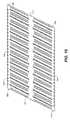
- FIG. 10is a schematic top view of a single printhead module including alignment features according to an embodiment of this invention.
- FIG. 11is a schematic top view of two adjacent printhead modules including complementary alignment features according to an embodiment of this invention.
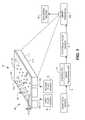
- FIG. 1a schematic representation of an inkjet printer system 10 suitable for use with the present invention is shown.
- Printer system 10is described in U.S. Pat. No. 7,350,902, the disclosure of which is incorporated by reference herein.
- Inkjet printer system 10includes an image data source 12 , which provides data signals that are interpreted by a controller 14 as being commands to eject drops.
- Controller 14includes an image processing unit 15 for rendering images for printing, and outputs signals to an electrical pulse source 16 of electrical energy pulses that are inputted to an inkjet printhead 100 , which includes at least one inkjet printhead die 110 .
- each of the two nozzle arrayshas two staggered rows of nozzles, each row having a nozzle density of 600 per inch.
- In fluid communication with each nozzle arrayis a corresponding ink delivery pathway.
- Ink delivery pathway 122is in fluid communication with the first nozzle array 120
- ink delivery pathway 132is in fluid communication with the second nozzle array 130 .
- Portions of fluid delivery pathways 122 and 132are shown in FIG. 1 as openings through printhead die substrate 111 .
- One or more inkjet printhead die 110are included in inkjet printhead 100 , but for greater clarity only one inkjet printhead die 110 is shown in FIG. 1 .
- the printhead dieare arranged on a support member as discussed below with reference to FIG. 2 . In FIG.
- first fluid source 18supplies ink to first nozzle array 120 via ink delivery pathway 122
- second fluid source 19supplies ink to second nozzle array 130 via ink delivery pathway 132 .
- distinct fluid sources 18 and 19are shown, in some applications it may be beneficial to have a single fluid source supplying ink to nozzle the first nozzle array 120 and the second nozzle array 130 via ink delivery pathways 122 and 132 respectively.
- fewer than two or more than two nozzle arraysmay be included on printhead die 110 .
- all nozzles on inkjet printhead die 110may be the same size, rather than having multiple sized nozzles on inkjet printhead die 110 .
- Drop forming mechanismsare associated with the nozzles.
- Drop forming mechanismscan be of a variety of types, some of which include a heating element to vaporize a portion of ink and thereby cause ejection of a droplet, or a piezoelectric transducer to constrict the volume of a fluid chamber and thereby cause ejection, or an actuator which is made to move (for example, by heating a bi-layer element) and thereby cause ejection.
- a drop ejectorincludes both a drop forming mechanism and a nozzle. Since each drop ejector includes a nozzle, a drop ejector array can also be called a nozzle array.
- Electrical pulses from electrical pulse source 16are sent to the various drop ejectors according to the desired deposition pattern.
- droplets 181 ejected from the first nozzle array 120are larger than droplets 182 ejected from the second nozzle array 130 , due to the larger nozzle opening area.
- droplets 181 ejected from the first nozzle array 120are larger than droplets 182 ejected from the second nozzle array 130 , due to the larger nozzle opening area.
- droplets 181 ejected from the first nozzle array 120are larger than droplets 182 ejected from the second nozzle array 130 , due to the larger nozzle opening area.
- droplets 181 ejected from the first nozzle array 120are larger than droplets 182 ejected from the second nozzle array 130 , due to the larger nozzle opening area.
- droplets of inkare deposited on a recording medium 20 .
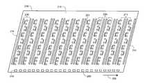
- FIG. 2shows a schematic top view of a modular printhead 200 according to an embodiment of this invention.
- Modular printhead 200includes three printhead modules 210 (similar to inkjet printhead die 110 but not having nozzles in staggered rows) that are bonded to a support member 205 .
- Each printhead module 205includes several arrays 211 of drop ejectors 212 , where the arrays 211 extend in a first direction 215 (also called array direction 215 ).
- Each printhead module 205has two butting edges 214 that are substantially parallel to first direction 215 , so that the arrays 211 are substantially parallel to the butting edges 214 of the printhead module 205 .
- a gapis shown between the butting edges 214 of adjacent printhead modules in order to distinguish the different printhead modules 205 .
- a portion of a sheet of recording medium 20is shown near the modular printhead 200 , and a raster line 22 of image data printed by modular printhead 200 is indicated.
- Array direction 215is at an angle ⁇ relative to raster line 22 .
- raster line 22has been broken up into three segments 22 a , 22 b and 22 c which are displaced from one another so that they may be more readily distinguished.
- the pixels in raster line segments 22 a , 22 b and 22 care printed by arrays 211 a , 211 b and 211 c respectively.
- Recording medium 20is moved along media advance direction 208 during printing.
- Drop ejectors 212 within an array 211are arranged such that the projection of the uppermost drop ejector of one array 211 onto raster line 22 is adjacent to the projection of the lowermost drop ejector of the adjacent array 211 onto raster line 22 .
- the uppermost drop ejector of one array 211is “projectionally adjacent” to the lowermost drop ejector of the adjacent array 211 .
- the printed dots making up raster line 22all have the same horizontal spacing.
- the spacing at the adjacent butting edges 214needs to be correct so that the projections of the uppermost drop ejector 212 and the lowermost drop ejector onto raster line 22 have the correct horizontal spacing and so that there is not a stitch error seen in the raster line 22 .
- adjacent die modules 210should not be displaced from one another along direction 208 , or displaced line segments will result at the stitch in the raster line 22 .
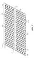
- a schematic top view of a single printhead module 210is shown magnified in FIG. 3 in order to clarify the geometry of the arrays 211 .
- the center to center distance between two corresponding nozzles in adjacent arrays 211is denoted as D.
- the center to center distance between two adjacent nozzles in the same array 211is denoted as d.
- the number of drop ejectors 212 within a single array 211is n.
- Dnd cos ⁇ .
- the distance from butting edge 214 to the nearest array 211is approximately D/2.
- n, d and ⁇when designing printhead module 210 , a large enough D/2 can be provided so that there is room for electronic circuitry, ink delivery, and alignment features between butting edge 214 and the nearest array 211 .
- d42.3 microns
- the length L of the printhead module 210is 13.54 mm.
- FIG. 4is a schematic top view of the example shown in FIG. 3 , but also showing additional details including ink inlets 220 , electronic circuitry 230 , and electrical contacts 240 .
- the ink inlets 220(shown in the example of FIG. 4 as staggered segments on both sides of each array 211 ) are of the dual feed type described in more detail in US Patent Application Publication No. US 2008/0180485 A1.
- Inkcan be fed from the back side of printhead module 210 to adjacent groups of drop ejectors by segmented ink inlets 220 consisting of slots 221 that can be made, for example, as described in U.S. patent application Ser. No. 12/241,747, filed Sep. 30, 2008, Lebens et al.
- Electronic circuitry 230can include driver transistors to provide electrical pulses from electrical pulse source 16 to fire the drop ejectors 212 , as well as logic electronics to control the driver transistors so that the correct drop ejectors 212 are fired at the proper time, according to image data provided by controller 14 and image processing unit 15 . Leads from the driver transistors are able to access the appropriate drop ejectors 212 from either side of array 211 between slots 221 . Electrical signals are provided to printhead module 210 by a plurality of electrical contacts 240 , which extend along one or both nonbutting edges 209 of printhead module 210 along direction 206 . Electrical contacts 240 are interconnected by wire bonding or tape automated bonding, for example, to a circuit board (not shown in FIG.
- each array 211 of drop ejectors 212including the arrays 211 nearest the butting edges 214 , has associated electronic circuitry 230 located on both sides of the array 211 .
- a portion of the electronic circuitry 230 on printhead module 210is located between a butting edge 214 and the array 211 of drop ejectors 212 that is closest to (and substantially parallel to) that butting edge 214 .
- FIG. 5is a schematic top view of an embodiment that is similar to that of FIG. 4 , but with a different type of ink inlets 220 , such that the ink flows continuously beneath the corresponding array 211 , from one end of the array to another end.
- the ink inlets 220have a first end 222 from which the ink flows (beneath the array 211 ) toward a second end 223 .
- Inkcan exit at the backside of printhead module 211 from second end 223 and be recirculated to enter at the backside near first end 222 .
- a second flow path(not shown in FIG. 5 , but optionally below the first flow path) can be provided opposite the first flow path in order to provide stagnation points adjacent each nozzle opening.
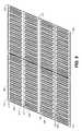
- FIG. 6is a schematic top view of a modular printhead 200 having a row 213 of three butted printhead modules 210 , according to an embodiment of this invention, but with more details provided for the printhead modules 210 than are provided in FIG. 2 .
- ink inlets 220 of the type shown in FIG. 5as well as electronic circuitry 230 , and electrical contacts 240 are shown.
- portions of electronic circuitry 230 located between a butting edge 214 and an adjacent array 211are shown for two adjacent printhead modules 210 .
- arrays 211 of drop ejectors 212extend along a first direction (array direction 215 ), and a plurality of electrical contacts 240 extend along a second direction (direction of plurality of electrical contacts 206 ), where the angle ⁇ between the first direction 215 and the second direction 206 is greater than 0 degrees and less than 90 degrees.
- Butting edges 214are substantially parallel to first direction 215 and nonbutting edges 209 are substantially parallel to second direction 206 .
- Alignment features(described below with reference to at least FIGS. 10 and 11 ) are contactable between adjacent printhead modules 210 .
- a second row of printhead modules 210can be provided on the support member 205 , where the second row of printhead modules 210 is parallel to row 213 .
- the second row of printhead modules 210can be used to print a different color ink, or different sized dots of the same color ink, or redundant dots of the same color ink in different embodiments.
- FIG. 7shows an embodiment of the present invention in which, rather than a second row of printhead modules 210 , two sets of independent arrays 211 a and 211 b are provided on a single printhead module 210 , such that a first array 216 of the arrays 21 la has a second corresponding array 217 of the arrays 211 b , where drop ejectors 212 in first array 216 line up (or offset at desired distance, e.g., 1 ⁇ 2 pixel) with drop ejectors 212 in corresponding second array 217 .
- Excellent alignment of drop ejectors 212 in first array 216 and drop ejectors 212 in corresponding second array 217is provided because first array 216 and corresponding second array 217 are fabricated together on the same printhead module 210 . Thus excellent registration of dots printed by drop ejectors in first array 216 and corresponding second array 217 is readily achieved.
- different colored inkwill be supplied at ink inlets 220 a for arrays 211 a than the ink supplied at ink inlets 220 b for arrays 220 b , so that the printhead module 210 of FIG. 7 can be a two-color printhead module.
- Four color printingcan be achieved by having two rows of two-color modules 210 on a support member 205 , for example.
- the same color inkis supplied at ink inlets 220 a and 220 b , and redundant drop ejectors 212 are thus provided in order to disguise print defects (as is well known in the art).
- the drop ejectors 212 in arrays 211 aprovide different sized ink drops than the drop ejectors 212 in arrays 211 b , smoother gradations in image tone can be provided.
- FIG. 8shows a row 213 of two butted printhead modules 210 a and 210 b of the type shown in FIG. 7 (two butted 2-color printhead modules, for example). Note that at the butting edges 214 , first array 216 a on printhead module 210 a has corresponding second array 217 b that is located on printhead module 210 b . Also note that first array 216 b on printhead module 210 b has no corresponding second array, and second array 217 a on printhead module 210 a has no corresponding first array. Thus, the very end arrays in a row 213 of printhead modules are not capable of full color printing, but that is typically small wastage.
- FIG. 9shows a printhead module 210 capable of four color printing (cyan, magenta, yellow and black), according to an embodiment of the present invention.
- a first array 216 and its corresponding second array 217 , corresponding third array 218 and corresponding fourth array 219are indicated.
- Electrical contacts 240 disposed along both nonbutting edges 209 of the printhead module 210provide signals for the electronic circuitry 230 corresponding to the arrays closest to the nonbutting edges of the printhead module 210 , as well as for the electronic circuitry corresponding to arrays within the interior of the printhead module 210 .
- the length of the printhead module 210(the distance between butting edges 214 ) was calculated to be 13.54 mm, and the distance between nonbutting edges 209 was estimated to be around 1.3 mm.
- the distance between butting edges 214would still be 13.54 mm, but the distance between nonbutting edges 209 would be about 5 mm.
- relative alignment of the printhead modules 210can be accomplished in various ways, for example, visually aligning the printhead modules. In other embodiments, however, alignment features can be provided such that when alignment features of adjacent printhead modules 210 contact each other, the printhead modules 210 are aligned with respect to each other.
- FIG. 10schematically shows a printhead module 210 having such alignment features according to an embodiment of this invention.
- the alignment featuresinclude two projections 252 on the butting edge 214 on the left side of the printhead module 210 , and two corresponding indentations 254 on the butting edge 214 on the right side of printhead module 210 .
- the projections 252are sized to fit into the indentations 254 of an adjacent printhead module 210 (see FIG. 11 ), such that when the projections 252 contact the indentations 254 of the adjacent printhead module 210 , the two printhead modules 210 are aligned relative to one another in two dimensions.
- the dimensions of the projections 252 and the corresponding indentations 254can be designed such that when projections 252 of one printhead module 210 contact the indentations 254 of an adjacent printhead module 210 , a gap 256 is provided at butting edge 214 , except at the contact points of the projections 252 and indentations 254 .
- Such a gap 256can be advantageous, in that there is less susceptibility to misalignment due to contamination or other unintended material being present at the butting edge 214 .
- a convenient place to locate the projections 252 and indentations 254 , as shown in FIG. 10is at the butting edge 214 , but near the nonbutting edge 209 , because there are typically no critical features such as electronic circuitry 230 adjacent the butting edge 215 near the nonbutting edge 209 .
- projections 252 and indentations 254 shown in FIG. 10is just one example of alignment features that can be used in different embodiments of the invention. Rather than having two projections 252 on one butting edge 214 and two indentations 254 on the other butting edge 214 , there can be a projection 252 near the top of one butting edge 214 and an indentation 254 near the bottom of that butting edge 214 . The other butting edge 214 would have an indentation 254 near the top and a projection 252 near the bottom.
- a first alignment feature on a first printhead modulecan include two projections 252
- a second alignment feature on a second printhead modulecan include two indentations 254 that are complementary to the two projections 252 of the first alignment feature, as in FIGS. 10 and 11 .
- the first alignment feature on the first printhead modulecan include a projection 252 and an indentation 254
- the second alignment feature on the second printhead modulecan include an indentation 254 and a projection 252 that are complementary to the projection 252 and indentation 254 of the first alignment feature.
- Projections 252 and indentations 254can have a variety of shapes, including triangular, trapezoidal, rounded, etc., as long as the indentations 254 of one printhead module 210 have the proper shape and dimensions to contact the projections 252 of the adjacent printhead module 210 and provide relative alignment of the two printhead modules 210 . Projections 252 and indentations 254 can have complementary shapes relative to one another.
- printhead modules 210are fabricated together on a single wafer.
- a printhead module 210 that is a thermal inkjet printhead dieis typically fabricated on a silicon wafer that is around six inches or eight inches in diameter. After wafer processing is completed, it is necessary to separate the individual printhead modules 210 from the wafer.
- the printhead modules 210can be separated from the wafer by dicing, even if the printhead module 210 is parallelogram-shaped. However, if edges of the printhead module 210 have projections 252 extending outward, such projections 252 would be cut off during dicing.
- One way to precisely form the projections 252 and the corresponding indentations 254is to use an etching process, such as deep reactive ion etching (commonly known in the art as DRIE).
- DRIEdeep reactive ion etching
- DRIEcan provide butting alignment features with accuracy on the order of 1 micron.
- FIG. 11was described above in relation to butting two adjacent printhead modules 210 together to assemble a modular printhead. However, FIG. 11 can also be used to describe the separation of two adjacent printhead modules 210 on a printhead wafer. As described above, the separation of adjacent printhead modules 210 at the projections 252 and corresponding indentations 254 on the adjacent module can be performed by DRIE.
- One method of achieving separation along the rest of the butting edge without cutting through projections 252is to use a cutting operation such as water jet or laser microjet, where nonstraight cuts are possible.
- a cutting operationsuch as water jet or laser microjet, where nonstraight cuts are possible.
- water jeta high pressure, high velocity stream of water cuts by erosion.
- laser microjeta pulsed laser beam is guided by a low pressure water jet, so that the water removes debris and cools the material.
- the width of the cut (or kerf) provided by water jet or laser microjetis typically wider than would be provided by DRIE at the projections 252 and indentations 254 , so that a gap 256 is provided between adjacent printhead modules 210 when they are subsequently butted with the corresponding projections 252 and indentations 254 in contact with one another.
- the precision and straightness of the portions of butting edge 214 that are cut by water jet or laser microjetdoes not need to be as good as that provided by DRIE to make the projections 252 and indentations 254 , because the gap 256 prevents those portions of the butting edge from coming into contact.
- Cutting of the nonbutting edges 209can be done with water jet or laser microjet. Alternatively, after separation along the butting edges 214 of all of the printhead modules 210 on the wafer has been completed, the adjacent nonbutting edges 209 can be cut by dicing.
Landscapes
- Particle Formation And Scattering Control In Inkjet Printers (AREA)
Abstract
Description
- 10 Inkjet printer system
- 12 Image data source
- 14 Controller
- 15 Image processing unit
- 16 Electrical pulse source
- 18 First fluid source
- 19 Second fluid source
- 20 Recording medium
- 22 Raster line
- 100 Inkjet printhead
- 110 Inkjet printhead die
- 111 Printhead die substrate
- 120 First nozzle array
- 121 Nozzle(s) in first nozzle array
- 122 Ink delivery pathway (for first nozzle array)
- 130 Second nozzle array
- 131 Nozzle(s) in second nozzle array
- 132 Ink delivery pathway (for second nozzle array)
- 181 Droplet(s) (ejected from first nozzle array)
- 182 Droplet(s) (ejected from second nozzle array)
- 200 Modular printhead
- 205 Support member
- 206 Direction of plurality of electrical contacts
- 208 Media advance direction
- 209 Nonbutting edge
- 210 Printhead module
- 211 Array(s) (of drop ejectors)
- 212 Drop ejector(s)
- 213 Row
- 214 Butting edge(s)
- 215 Array direction
- 216 First array
- 217 Corresponding second array
- 218 Corresponding third array
- 219 Corresponding fourth array
- 220 Ink inlet(s)
- 221 Slots
- 230 Electronic circuitry
- 240 Electrical contacts
- 252 Alignment feature (projection)
- 254 Alignment feature (indentation)
- 256 Gap
Claims (23)
Priority Applications (6)
| Application Number | Priority Date | Filing Date | Title |
|---|---|---|---|
| US12/337,665US8118405B2 (en) | 2008-12-18 | 2008-12-18 | Buttable printhead module and pagewide printhead |
| CN200980151026.3ACN102256800B (en) | 2008-12-18 | 2009-12-16 | Dockable printhead modules and pagewidth printheads |
| EP11194779AEP2436521B1 (en) | 2008-12-18 | 2009-12-16 | Method of forming a buttable printhead module in a pagewide printhead |
| JP2011542132AJP2012512769A (en) | 2008-12-18 | 2009-12-16 | Matchable print head module and page width print head |
| EP09795839AEP2379333A2 (en) | 2008-12-18 | 2009-12-16 | Buttable printhead module and pagewide printhead |
| PCT/US2009/006595WO2010080114A2 (en) | 2008-12-18 | 2009-12-16 | Buttable printhead module and pagewide printhead |
Applications Claiming Priority (1)
| Application Number | Priority Date | Filing Date | Title |
|---|---|---|---|
| US12/337,665US8118405B2 (en) | 2008-12-18 | 2008-12-18 | Buttable printhead module and pagewide printhead |
Publications (2)
| Publication Number | Publication Date |
|---|---|
| US20100156992A1 US20100156992A1 (en) | 2010-06-24 |
| US8118405B2true US8118405B2 (en) | 2012-02-21 |
Family
ID=41845275
Family Applications (1)
| Application Number | Title | Priority Date | Filing Date |
|---|---|---|---|
| US12/337,665Expired - Fee RelatedUS8118405B2 (en) | 2008-12-18 | 2008-12-18 | Buttable printhead module and pagewide printhead |
Country Status (5)
| Country | Link |
|---|---|
| US (1) | US8118405B2 (en) |
| EP (2) | EP2436521B1 (en) |
| JP (1) | JP2012512769A (en) |
| CN (1) | CN102256800B (en) |
| WO (1) | WO2010080114A2 (en) |
Cited By (8)
| Publication number | Priority date | Publication date | Assignee | Title |
|---|---|---|---|---|
| US20110292122A1 (en)* | 2010-05-27 | 2011-12-01 | Frank Edward Anderson | Skewed nozzle arrays on ejection chips for micro-fluid applications |
| US20120127238A1 (en)* | 2010-11-18 | 2012-05-24 | Xerox Corporation | Inkjet ejector arrays aligned to a curved image receiving surface with ink recirculation |
| US20170282562A1 (en)* | 2016-03-31 | 2017-10-05 | Brother Kogyo Kabushiki Kaisha | Liquid jetting apparatus |
| US9840075B1 (en)* | 2016-06-14 | 2017-12-12 | RF Printing Technologies LLC | Printing method with multiple aligned drop ejectors |
| US10166769B2 (en) | 2016-06-14 | 2019-01-01 | RF Printing Technologies LLC | Inkjet printhead with multiple aligned drop ejectors |
| DE112017002506T5 (en) | 2016-06-14 | 2019-03-14 | RF Printing Technologies LLC | An inkjet printhead having a plurality of aligned drop ejectors and method of using the same during printing |
| US10336074B1 (en)* | 2018-01-18 | 2019-07-02 | Rf Printing Technologies | Inkjet printhead with hierarchically aligned printhead units |
| US11975468B2 (en) | 2019-07-26 | 2024-05-07 | Hewlett-Packard Development Company, L.P. | Coplanar modular printbars |
Families Citing this family (11)
| Publication number | Priority date | Publication date | Assignee | Title |
|---|---|---|---|---|
| CN104512105B (en)* | 2013-09-26 | 2016-10-05 | 研能科技股份有限公司 | Printing unit that can be shared with general inkjet printing and page width printing |
| JP6659089B2 (en)* | 2014-05-13 | 2020-03-04 | キヤノン株式会社 | Liquid ejection head |
| JP6659088B2 (en)* | 2014-05-13 | 2020-03-04 | キヤノン株式会社 | Liquid ejection head |
| US9895892B2 (en)* | 2015-11-18 | 2018-02-20 | Ricoh Company, Ltd. | Head unit and liquid discharge apparatus including same |
| JP6821331B2 (en)* | 2016-05-30 | 2021-01-27 | キヤノン株式会社 | Recording element substrate, liquid discharge head, and liquid discharge device |
| TW201838829A (en)* | 2017-02-06 | 2018-11-01 | 愛爾蘭商滿捷特科技公司 | Inkjet print head for full color page wide printing |
| KR102390902B1 (en) | 2017-10-16 | 2022-04-25 | 엘지전자 주식회사 | Image display apparatus |
| CN113365838B (en) | 2019-02-06 | 2022-12-13 | 惠普发展公司,有限责任合伙企业 | Fluidic die and integrated circuit thereof, method of operating a fluidic die |
| WO2020162898A1 (en) | 2019-02-06 | 2020-08-13 | Hewlett-Packard Development Company, L.P. | Identifying random bits in control data packets |
| US11364719B2 (en)* | 2019-02-06 | 2022-06-21 | Hewlett-Packard Development Company, L.P. | Print component with memory array using intermittent clock signal |
| CN111532027B (en)* | 2020-05-13 | 2025-04-25 | 苏州锐发打印技术有限公司 | Piezoelectric inkjet print head and printing system |
Citations (28)
| Publication number | Priority date | Publication date | Assignee | Title |
|---|---|---|---|---|
| US4463359A (en) | 1979-04-02 | 1984-07-31 | Canon Kabushiki Kaisha | Droplet generating method and apparatus thereof |
| US4822755A (en) | 1988-04-25 | 1989-04-18 | Xerox Corporation | Method of fabricating large area semiconductor arrays |
| US4961821A (en) | 1989-11-22 | 1990-10-09 | Xerox Corporation | Ode through holes and butt edges without edge dicing |
| US4985710A (en) | 1989-11-29 | 1991-01-15 | Xerox Corporation | Buttable subunits for pagewidth "Roofshooter" printheads |
| US5079189A (en) | 1990-06-18 | 1992-01-07 | Xerox Corporation | Method of making RIS or ROS array bars using replaceable subunits |
| US5098503A (en) | 1990-05-01 | 1992-03-24 | Xerox Corporation | Method of fabricating precision pagewidth assemblies of ink jet subunits |
| US5160403A (en) | 1991-08-09 | 1992-11-03 | Xerox Corporation | Precision diced aligning surfaces for devices such as ink jet printheads |
| US5198054A (en) | 1991-08-12 | 1993-03-30 | Xerox Corporation | Method of making compensated collinear reading or writing bar arrays assembled from subunits |
| JPH05162319A (en) | 1991-12-12 | 1993-06-29 | Canon Inc | INKJET RECORDING HEAD, MANUFACTURING METHOD THEREOF, AND INKJET RECORDING DEVICE HAVING THE HEAD |
| US5257043A (en) | 1991-12-09 | 1993-10-26 | Xerox Corporation | Thermal ink jet nozzle arrays |
| US5572244A (en) | 1994-07-27 | 1996-11-05 | Xerox Corporation | Adhesive-free edge butting for printhead elements |
| US5620614A (en) | 1995-01-03 | 1997-04-15 | Xerox Corporation | Printhead array and method of producing a printhead die assembly that minimizes end channel damage |
| US5706176A (en) | 1996-07-22 | 1998-01-06 | Xerox Corporation | Butted chip array with beveled chips |
| US5719605A (en) | 1996-11-20 | 1998-02-17 | Lexmark International, Inc. | Large array heater chips for thermal ink jet printheads |
| EP0914950A2 (en) | 1997-11-06 | 1999-05-12 | Xerox Corporation | An ink jet printhead assembled from partial width array printheads |
| US6428142B1 (en) | 1999-12-09 | 2002-08-06 | Silverbrook Research Pty Ltd | Four color modular printhead system |
| US6575561B1 (en) | 2000-03-09 | 2003-06-10 | Silverbrook Research Pty Ltd | Modular printhead alignment system |
| US6623106B2 (en) | 2000-03-02 | 2003-09-23 | Silverbrook Research Pty Ltd | Overlapping printhead module array configuration |
| US6655786B1 (en) | 2000-10-20 | 2003-12-02 | Silverbrook Research Pty Ltd | Mounting of printhead in support member of six color inkjet modular printhead |
| WO2004056572A2 (en) | 2002-12-20 | 2004-07-08 | Xaar Technology Limited | Droplet deposition apparatus |
| US20040218013A1 (en) | 2001-03-27 | 2004-11-04 | Kia Silverbrook | Pagewidth printer having modular printhead assembly with flexible PCB and busbars |
| US20050046669A1 (en) | 2000-03-02 | 2005-03-03 | Kia Silverbrook | Manually alignment mechanism for printhead modules |
| US20060152547A1 (en) | 2000-12-07 | 2006-07-13 | Kia Silverbrook | Printhead system having closely arranged printhead modules |
| US20070206051A1 (en) | 2001-03-27 | 2007-09-06 | Silverbrook Research Pty Ltd | Method For Assembling A Modular Printhead Assembly |
| US20070206052A1 (en) | 1997-07-15 | 2007-09-06 | Silverbrook Research Pty Ltd | Print assembly and printer having wide printing zone |
| US20070291082A1 (en) | 2006-06-20 | 2007-12-20 | Baumer Michael F | Drop on demand print head with fluid stagnation point at nozzle opening |
| US7350902B2 (en) | 2004-11-18 | 2008-04-01 | Eastman Kodak Company | Fluid ejection device nozzle array configuration |
| US20080180485A1 (en) | 2007-01-25 | 2008-07-31 | Delametter Christopher N | Dual feed liquid drop ejector |
Family Cites Families (4)
| Publication number | Priority date | Publication date | Assignee | Title |
|---|---|---|---|---|
| US5939206A (en)* | 1996-08-29 | 1999-08-17 | Xerox Corporation | Stabilized porous, electrically conductive substrates |
| JP2001260366A (en)* | 2000-03-21 | 2001-09-25 | Nec Corp | Ink jet recording head and its manufacturing method |
| JP4827668B2 (en)* | 2006-09-11 | 2011-11-30 | 富士フイルム株式会社 | Liquid discharge head and method of manufacturing liquid discharge head |
| JP4221615B2 (en)* | 2007-04-13 | 2009-02-12 | ブラザー工業株式会社 | Inkjet printer head and piezoelectric actuator |
- 2008
- 2008-12-18USUS12/337,665patent/US8118405B2/ennot_activeExpired - Fee Related
- 2009
- 2009-12-16JPJP2011542132Apatent/JP2012512769A/enactivePending
- 2009-12-16EPEP11194779Apatent/EP2436521B1/ennot_activeNot-in-force
- 2009-12-16WOPCT/US2009/006595patent/WO2010080114A2/enactiveApplication Filing
- 2009-12-16EPEP09795839Apatent/EP2379333A2/ennot_activeWithdrawn
- 2009-12-16CNCN200980151026.3Apatent/CN102256800B/ennot_activeExpired - Fee Related
Patent Citations (28)
| Publication number | Priority date | Publication date | Assignee | Title |
|---|---|---|---|---|
| US4463359A (en) | 1979-04-02 | 1984-07-31 | Canon Kabushiki Kaisha | Droplet generating method and apparatus thereof |
| US4822755A (en) | 1988-04-25 | 1989-04-18 | Xerox Corporation | Method of fabricating large area semiconductor arrays |
| US4961821A (en) | 1989-11-22 | 1990-10-09 | Xerox Corporation | Ode through holes and butt edges without edge dicing |
| US4985710A (en) | 1989-11-29 | 1991-01-15 | Xerox Corporation | Buttable subunits for pagewidth "Roofshooter" printheads |
| US5098503A (en) | 1990-05-01 | 1992-03-24 | Xerox Corporation | Method of fabricating precision pagewidth assemblies of ink jet subunits |
| US5079189A (en) | 1990-06-18 | 1992-01-07 | Xerox Corporation | Method of making RIS or ROS array bars using replaceable subunits |
| US5160403A (en) | 1991-08-09 | 1992-11-03 | Xerox Corporation | Precision diced aligning surfaces for devices such as ink jet printheads |
| US5198054A (en) | 1991-08-12 | 1993-03-30 | Xerox Corporation | Method of making compensated collinear reading or writing bar arrays assembled from subunits |
| US5257043A (en) | 1991-12-09 | 1993-10-26 | Xerox Corporation | Thermal ink jet nozzle arrays |
| JPH05162319A (en) | 1991-12-12 | 1993-06-29 | Canon Inc | INKJET RECORDING HEAD, MANUFACTURING METHOD THEREOF, AND INKJET RECORDING DEVICE HAVING THE HEAD |
| US5572244A (en) | 1994-07-27 | 1996-11-05 | Xerox Corporation | Adhesive-free edge butting for printhead elements |
| US5620614A (en) | 1995-01-03 | 1997-04-15 | Xerox Corporation | Printhead array and method of producing a printhead die assembly that minimizes end channel damage |
| US5706176A (en) | 1996-07-22 | 1998-01-06 | Xerox Corporation | Butted chip array with beveled chips |
| US5719605A (en) | 1996-11-20 | 1998-02-17 | Lexmark International, Inc. | Large array heater chips for thermal ink jet printheads |
| US20070206052A1 (en) | 1997-07-15 | 2007-09-06 | Silverbrook Research Pty Ltd | Print assembly and printer having wide printing zone |
| EP0914950A2 (en) | 1997-11-06 | 1999-05-12 | Xerox Corporation | An ink jet printhead assembled from partial width array printheads |
| US6428142B1 (en) | 1999-12-09 | 2002-08-06 | Silverbrook Research Pty Ltd | Four color modular printhead system |
| US6623106B2 (en) | 2000-03-02 | 2003-09-23 | Silverbrook Research Pty Ltd | Overlapping printhead module array configuration |
| US20050046669A1 (en) | 2000-03-02 | 2005-03-03 | Kia Silverbrook | Manually alignment mechanism for printhead modules |
| US6575561B1 (en) | 2000-03-09 | 2003-06-10 | Silverbrook Research Pty Ltd | Modular printhead alignment system |
| US6655786B1 (en) | 2000-10-20 | 2003-12-02 | Silverbrook Research Pty Ltd | Mounting of printhead in support member of six color inkjet modular printhead |
| US20060152547A1 (en) | 2000-12-07 | 2006-07-13 | Kia Silverbrook | Printhead system having closely arranged printhead modules |
| US20040218013A1 (en) | 2001-03-27 | 2004-11-04 | Kia Silverbrook | Pagewidth printer having modular printhead assembly with flexible PCB and busbars |
| US20070206051A1 (en) | 2001-03-27 | 2007-09-06 | Silverbrook Research Pty Ltd | Method For Assembling A Modular Printhead Assembly |
| WO2004056572A2 (en) | 2002-12-20 | 2004-07-08 | Xaar Technology Limited | Droplet deposition apparatus |
| US7350902B2 (en) | 2004-11-18 | 2008-04-01 | Eastman Kodak Company | Fluid ejection device nozzle array configuration |
| US20070291082A1 (en) | 2006-06-20 | 2007-12-20 | Baumer Michael F | Drop on demand print head with fluid stagnation point at nozzle opening |
| US20080180485A1 (en) | 2007-01-25 | 2008-07-31 | Delametter Christopher N | Dual feed liquid drop ejector |
Cited By (20)
| Publication number | Priority date | Publication date | Assignee | Title |
|---|---|---|---|---|
| US20110292122A1 (en)* | 2010-05-27 | 2011-12-01 | Frank Edward Anderson | Skewed nozzle arrays on ejection chips for micro-fluid applications |
| US8777376B2 (en)* | 2010-05-27 | 2014-07-15 | Funai Electric Co., Ltd. | Skewed nozzle arrays on ejection chips for micro-fluid applications |
| US20120127238A1 (en)* | 2010-11-18 | 2012-05-24 | Xerox Corporation | Inkjet ejector arrays aligned to a curved image receiving surface with ink recirculation |
| US8317298B2 (en)* | 2010-11-18 | 2012-11-27 | Xerox Corporation | Inkjet ejector arrays aligned to a curved image receiving surface with ink recirculation |
| US8668308B2 (en) | 2010-11-18 | 2014-03-11 | Xerox Corporation | Inkjet ejector arrays aligned to a curved image receiving surface with ink recirculation |
| US10807369B2 (en) | 2016-03-31 | 2020-10-20 | Brother Kogyo Kabushiki Kaisha | Liquid jetting apparatus |
| US10336075B2 (en) | 2016-03-31 | 2019-07-02 | Brother Kogyo Kabushiki Kaisha | Inkjet head arrangement and control of liquid jetting apparatus |
| US11660868B2 (en) | 2016-03-31 | 2023-05-30 | Brother Kogyo Kabushiki Kaisha | Liquid jetting apparatus capable of jetting a plurality of kinds of liquid |
| US10022967B2 (en)* | 2016-03-31 | 2018-07-17 | Brother Kogyo Kabushiki Kaisha | Liquid jetting apparatus |
| US11155092B2 (en) | 2016-03-31 | 2021-10-26 | Brother Kogyo Kabushiki Kaisha | Liquid jetting apparatus capable of jetting a plurality of kinds of liquid |
| US20170282562A1 (en)* | 2016-03-31 | 2017-10-05 | Brother Kogyo Kabushiki Kaisha | Liquid jetting apparatus |
| US10166769B2 (en) | 2016-06-14 | 2019-01-01 | RF Printing Technologies LLC | Inkjet printhead with multiple aligned drop ejectors |
| CN109476157A (en)* | 2016-06-14 | 2019-03-15 | Rf打印技术有限责任公司 | There are the inkjet print head and its application method of multiple alignment liquid drop ejectors |
| DE112017002506T5 (en) | 2016-06-14 | 2019-03-14 | RF Printing Technologies LLC | An inkjet printhead having a plurality of aligned drop ejectors and method of using the same during printing |
| US9840075B1 (en)* | 2016-06-14 | 2017-12-12 | RF Printing Technologies LLC | Printing method with multiple aligned drop ejectors |
| US20170355189A1 (en)* | 2016-06-14 | 2017-12-14 | RF Printing Technologies LLC | Printing method with multiple aligned drop ejectors |
| US10336074B1 (en)* | 2018-01-18 | 2019-07-02 | Rf Printing Technologies | Inkjet printhead with hierarchically aligned printhead units |
| CN109986884A (en)* | 2018-01-18 | 2019-07-09 | Rf打印技术有限责任公司 | The inkjet print head of printhead unit containing classification alignment |
| TWI714946B (en)* | 2018-01-18 | 2021-01-01 | 大陸商上海銳爾發數碼科技有限公司 | Inkjet printhead with hierarchically aligned printhead units |
| US11975468B2 (en) | 2019-07-26 | 2024-05-07 | Hewlett-Packard Development Company, L.P. | Coplanar modular printbars |
Also Published As
| Publication number | Publication date |
|---|---|
| EP2436521A1 (en) | 2012-04-04 |
| WO2010080114A2 (en) | 2010-07-15 |
| EP2379333A2 (en) | 2011-10-26 |
| US20100156992A1 (en) | 2010-06-24 |
| CN102256800B (en) | 2014-09-10 |
| CN102256800A (en) | 2011-11-23 |
| WO2010080114A3 (en) | 2010-08-26 |
| JP2012512769A (en) | 2012-06-07 |
| EP2436521B1 (en) | 2013-04-03 |
Similar Documents
| Publication | Publication Date | Title |
|---|---|---|
| US8118405B2 (en) | Buttable printhead module and pagewide printhead | |
| EP1827847B1 (en) | Fluid ejection device nozzle array configuration | |
| US8496318B2 (en) | Liquid drop ejection using dual feed ejector | |
| EP1232864B1 (en) | Continuous ink jet printhead | |
| US8087759B2 (en) | Print head with offset ejection ports | |
| US8591008B2 (en) | Liquid drop ejection using dual feed ejector | |
| US6536883B2 (en) | Continuous ink-jet printer having two dimensional nozzle array and method of increasing ink drop density | |
| JP2006123550A (en) | NOZZLE PLATE, INKJET PRINT HEAD HAVING THE SAME, AND METHOD FOR PRODUCING NOZZLE PLATE | |
| US8474951B2 (en) | Liquid ejection head | |
| US6779861B2 (en) | Enhanced dot resolution for inkjet printing | |
| JP2002160368A (en) | Print head | |
| JP2004001488A (en) | Inkjet head | |
| US7980662B2 (en) | Ink jet print head | |
| US20090295861A1 (en) | Continuous fluid jet ejector with anisotropically etched fluid chambers | |
| US8449086B2 (en) | Inkjet chamber and inlets for circulating flow | |
| JP2009051081A (en) | Droplet discharge head, integrated droplet discharge head unit, and image forming apparatus | |
| US7909434B2 (en) | Printhead and method of printing | |
| JP2007296696A (en) | Droplet discharge device | |
| CN212289183U (en) | Printing apparatus | |
| JP2009012369A (en) | Fluid ejecting apparatus and fluid ejecting method | |
| US20240391238A1 (en) | Ink jet print head nozzle matrix layout | |
| US20120249687A1 (en) | Inkjet chamber refill method with circulating flow | |
| JP2000190499A (en) | Top heater type thermal inkjet head | |
| JP2017124518A (en) | Liquid ejecting head and liquid ejecting apparatus |
Legal Events
| Date | Code | Title | Description |
|---|---|---|---|
| AS | Assignment | Owner name:EASTMAN KODAK COMPANY,NEW YORK Free format text:ASSIGNMENT OF ASSIGNORS INTEREST;ASSIGNORS:XIE, YONGLIN;MORTON, CHRISTOPHER R.;KNEEZEL, GARY A.;SIGNING DATES FROM 20081216 TO 20081217;REEL/FRAME:022000/0357 Owner name:EASTMAN KODAK COMPANY, NEW YORK Free format text:ASSIGNMENT OF ASSIGNORS INTEREST;ASSIGNORS:XIE, YONGLIN;MORTON, CHRISTOPHER R.;KNEEZEL, GARY A.;SIGNING DATES FROM 20081216 TO 20081217;REEL/FRAME:022000/0357 | |
| FEPP | Fee payment procedure | Free format text:PAYER NUMBER DE-ASSIGNED (ORIGINAL EVENT CODE: RMPN); ENTITY STATUS OF PATENT OWNER: LARGE ENTITY Free format text:PAYOR NUMBER ASSIGNED (ORIGINAL EVENT CODE: ASPN); ENTITY STATUS OF PATENT OWNER: LARGE ENTITY | |
| STCF | Information on status: patent grant | Free format text:PATENTED CASE | |
| AS | Assignment | Owner name:CITICORP NORTH AMERICA, INC., AS AGENT, NEW YORK Free format text:SECURITY INTEREST;ASSIGNORS:EASTMAN KODAK COMPANY;PAKON, INC.;REEL/FRAME:028201/0420 Effective date:20120215 | |
| AS | Assignment | Owner name:WILMINGTON TRUST, NATIONAL ASSOCIATION, AS AGENT, MINNESOTA Free format text:PATENT SECURITY AGREEMENT;ASSIGNORS:EASTMAN KODAK COMPANY;PAKON, INC.;REEL/FRAME:030122/0235 Effective date:20130322 Owner name:WILMINGTON TRUST, NATIONAL ASSOCIATION, AS AGENT, Free format text:PATENT SECURITY AGREEMENT;ASSIGNORS:EASTMAN KODAK COMPANY;PAKON, INC.;REEL/FRAME:030122/0235 Effective date:20130322 | |
| AS | Assignment | Owner name:BANK OF AMERICA N.A., AS AGENT, MASSACHUSETTS Free format text:INTELLECTUAL PROPERTY SECURITY AGREEMENT (ABL);ASSIGNORS:EASTMAN KODAK COMPANY;FAR EAST DEVELOPMENT LTD.;FPC INC.;AND OTHERS;REEL/FRAME:031162/0117 Effective date:20130903 Owner name:BARCLAYS BANK PLC, AS ADMINISTRATIVE AGENT, NEW YORK Free format text:INTELLECTUAL PROPERTY SECURITY AGREEMENT (SECOND LIEN);ASSIGNORS:EASTMAN KODAK COMPANY;FAR EAST DEVELOPMENT LTD.;FPC INC.;AND OTHERS;REEL/FRAME:031159/0001 Effective date:20130903 Owner name:JPMORGAN CHASE BANK, N.A., AS ADMINISTRATIVE, DELAWARE Free format text:INTELLECTUAL PROPERTY SECURITY AGREEMENT (FIRST LIEN);ASSIGNORS:EASTMAN KODAK COMPANY;FAR EAST DEVELOPMENT LTD.;FPC INC.;AND OTHERS;REEL/FRAME:031158/0001 Effective date:20130903 Owner name:PAKON, INC., NEW YORK Free format text:RELEASE OF SECURITY INTEREST IN PATENTS;ASSIGNORS:CITICORP NORTH AMERICA, INC., AS SENIOR DIP AGENT;WILMINGTON TRUST, NATIONAL ASSOCIATION, AS JUNIOR DIP AGENT;REEL/FRAME:031157/0451 Effective date:20130903 Owner name:EASTMAN KODAK COMPANY, NEW YORK Free format text:RELEASE OF SECURITY INTEREST IN PATENTS;ASSIGNORS:CITICORP NORTH AMERICA, INC., AS SENIOR DIP AGENT;WILMINGTON TRUST, NATIONAL ASSOCIATION, AS JUNIOR DIP AGENT;REEL/FRAME:031157/0451 Effective date:20130903 Owner name:JPMORGAN CHASE BANK, N.A., AS ADMINISTRATIVE, DELA Free format text:INTELLECTUAL PROPERTY SECURITY AGREEMENT (FIRST LIEN);ASSIGNORS:EASTMAN KODAK COMPANY;FAR EAST DEVELOPMENT LTD.;FPC INC.;AND OTHERS;REEL/FRAME:031158/0001 Effective date:20130903 Owner name:BARCLAYS BANK PLC, AS ADMINISTRATIVE AGENT, NEW YO Free format text:INTELLECTUAL PROPERTY SECURITY AGREEMENT (SECOND LIEN);ASSIGNORS:EASTMAN KODAK COMPANY;FAR EAST DEVELOPMENT LTD.;FPC INC.;AND OTHERS;REEL/FRAME:031159/0001 Effective date:20130903 | |
| FPAY | Fee payment | Year of fee payment:4 | |
| AS | Assignment | Owner name:KODAK PORTUGUESA LIMITED, NEW YORK Free format text:RELEASE BY SECURED PARTY;ASSIGNOR:JP MORGAN CHASE BANK, N.A., AS ADMINISTRATIVE AGENT;REEL/FRAME:050239/0001 Effective date:20190617 Owner name:EASTMAN KODAK COMPANY, NEW YORK Free format text:RELEASE BY SECURED PARTY;ASSIGNOR:JP MORGAN CHASE BANK, N.A., AS ADMINISTRATIVE AGENT;REEL/FRAME:050239/0001 Effective date:20190617 Owner name:KODAK AMERICAS, LTD., NEW YORK Free format text:RELEASE BY SECURED PARTY;ASSIGNOR:JP MORGAN CHASE BANK, N.A., AS ADMINISTRATIVE AGENT;REEL/FRAME:050239/0001 Effective date:20190617 Owner name:KODAK PHILIPPINES, LTD., NEW YORK Free format text:RELEASE BY SECURED PARTY;ASSIGNOR:JP MORGAN CHASE BANK, N.A., AS ADMINISTRATIVE AGENT;REEL/FRAME:050239/0001 Effective date:20190617 Owner name:KODAK IMAGING NETWORK, INC., NEW YORK Free format text:RELEASE BY SECURED PARTY;ASSIGNOR:JP MORGAN CHASE BANK, N.A., AS ADMINISTRATIVE AGENT;REEL/FRAME:050239/0001 Effective date:20190617 Owner name:FAR EAST DEVELOPMENT LTD., NEW YORK Free format text:RELEASE BY SECURED PARTY;ASSIGNOR:JP MORGAN CHASE BANK, N.A., AS ADMINISTRATIVE AGENT;REEL/FRAME:050239/0001 Effective date:20190617 Owner name:KODAK (NEAR EAST), INC., NEW YORK Free format text:RELEASE BY SECURED PARTY;ASSIGNOR:JP MORGAN CHASE BANK, N.A., AS ADMINISTRATIVE AGENT;REEL/FRAME:050239/0001 Effective date:20190617 Owner name:KODAK AVIATION LEASING LLC, NEW YORK Free format text:RELEASE BY SECURED PARTY;ASSIGNOR:JP MORGAN CHASE BANK, N.A., AS ADMINISTRATIVE AGENT;REEL/FRAME:050239/0001 Effective date:20190617 Owner name:NPEC, INC., NEW YORK Free format text:RELEASE BY SECURED PARTY;ASSIGNOR:JP MORGAN CHASE BANK, N.A., AS ADMINISTRATIVE AGENT;REEL/FRAME:050239/0001 Effective date:20190617 Owner name:LASER PACIFIC MEDIA CORPORATION, NEW YORK Free format text:RELEASE BY SECURED PARTY;ASSIGNOR:JP MORGAN CHASE BANK, N.A., AS ADMINISTRATIVE AGENT;REEL/FRAME:050239/0001 Effective date:20190617 Owner name:QUALEX, INC., NEW YORK Free format text:RELEASE BY SECURED PARTY;ASSIGNOR:JP MORGAN CHASE BANK, N.A., AS ADMINISTRATIVE AGENT;REEL/FRAME:050239/0001 Effective date:20190617 Owner name:FPC, INC., NEW YORK Free format text:RELEASE BY SECURED PARTY;ASSIGNOR:JP MORGAN CHASE BANK, N.A., AS ADMINISTRATIVE AGENT;REEL/FRAME:050239/0001 Effective date:20190617 Owner name:KODAK REALTY, INC., NEW YORK Free format text:RELEASE BY SECURED PARTY;ASSIGNOR:JP MORGAN CHASE BANK, N.A., AS ADMINISTRATIVE AGENT;REEL/FRAME:050239/0001 Effective date:20190617 Owner name:CREO MANUFACTURING AMERICA LLC, NEW YORK Free format text:RELEASE BY SECURED PARTY;ASSIGNOR:JP MORGAN CHASE BANK, N.A., AS ADMINISTRATIVE AGENT;REEL/FRAME:050239/0001 Effective date:20190617 Owner name:PAKON, INC., NEW YORK Free format text:RELEASE BY SECURED PARTY;ASSIGNOR:JP MORGAN CHASE BANK, N.A., AS ADMINISTRATIVE AGENT;REEL/FRAME:050239/0001 Effective date:20190617 | |
| AS | Assignment | Owner name:PFC, INC., NEW YORK Free format text:RELEASE BY SECURED PARTY;ASSIGNOR:JP MORGAN CHASE BANK, N.A., AS ADMINISTRATIVE AGENT;REEL/FRAME:049901/0001 Effective date:20190617 Owner name:KODAK PHILIPPINES, LTD., NEW YORK Free format text:RELEASE BY SECURED PARTY;ASSIGNOR:JP MORGAN CHASE BANK, N.A., AS ADMINISTRATIVE AGENT;REEL/FRAME:049901/0001 Effective date:20190617 Owner name:KODAK REALTY, INC., NEW YORK Free format text:RELEASE BY SECURED PARTY;ASSIGNOR:JP MORGAN CHASE BANK, N.A., AS ADMINISTRATIVE AGENT;REEL/FRAME:049901/0001 Effective date:20190617 Owner name:QUALEX, INC., NEW YORK Free format text:RELEASE BY SECURED PARTY;ASSIGNOR:JP MORGAN CHASE BANK, N.A., AS ADMINISTRATIVE AGENT;REEL/FRAME:049901/0001 Effective date:20190617 Owner name:KODAK (NEAR EAST), INC., NEW YORK Free format text:RELEASE BY SECURED PARTY;ASSIGNOR:JP MORGAN CHASE BANK, N.A., AS ADMINISTRATIVE AGENT;REEL/FRAME:049901/0001 Effective date:20190617 Owner name:KODAK AMERICAS, LTD., NEW YORK Free format text:RELEASE BY SECURED PARTY;ASSIGNOR:JP MORGAN CHASE BANK, N.A., AS ADMINISTRATIVE AGENT;REEL/FRAME:049901/0001 Effective date:20190617 Owner name:EASTMAN KODAK COMPANY, NEW YORK Free format text:RELEASE BY SECURED PARTY;ASSIGNOR:JP MORGAN CHASE BANK, N.A., AS ADMINISTRATIVE AGENT;REEL/FRAME:049901/0001 Effective date:20190617 Owner name:KODAK PORTUGUESA LIMITED, NEW YORK Free format text:RELEASE BY SECURED PARTY;ASSIGNOR:JP MORGAN CHASE BANK, N.A., AS ADMINISTRATIVE AGENT;REEL/FRAME:049901/0001 Effective date:20190617 Owner name:PAKON, INC., NEW YORK Free format text:RELEASE BY SECURED PARTY;ASSIGNOR:JP MORGAN CHASE BANK, N.A., AS ADMINISTRATIVE AGENT;REEL/FRAME:049901/0001 Effective date:20190617 Owner name:FAR EAST DEVELOPMENT LTD., NEW YORK Free format text:RELEASE BY SECURED PARTY;ASSIGNOR:JP MORGAN CHASE BANK, N.A., AS ADMINISTRATIVE AGENT;REEL/FRAME:049901/0001 Effective date:20190617 Owner name:LASER PACIFIC MEDIA CORPORATION, NEW YORK Free format text:RELEASE BY SECURED PARTY;ASSIGNOR:JP MORGAN CHASE BANK, N.A., AS ADMINISTRATIVE AGENT;REEL/FRAME:049901/0001 Effective date:20190617 Owner name:CREO MANUFACTURING AMERICA LLC, NEW YORK Free format text:RELEASE BY SECURED PARTY;ASSIGNOR:JP MORGAN CHASE BANK, N.A., AS ADMINISTRATIVE AGENT;REEL/FRAME:049901/0001 Effective date:20190617 Owner name:KODAK IMAGING NETWORK, INC., NEW YORK Free format text:RELEASE BY SECURED PARTY;ASSIGNOR:JP MORGAN CHASE BANK, N.A., AS ADMINISTRATIVE AGENT;REEL/FRAME:049901/0001 Effective date:20190617 Owner name:KODAK AVIATION LEASING LLC, NEW YORK Free format text:RELEASE BY SECURED PARTY;ASSIGNOR:JP MORGAN CHASE BANK, N.A., AS ADMINISTRATIVE AGENT;REEL/FRAME:049901/0001 Effective date:20190617 Owner name:NPEC, INC., NEW YORK Free format text:RELEASE BY SECURED PARTY;ASSIGNOR:JP MORGAN CHASE BANK, N.A., AS ADMINISTRATIVE AGENT;REEL/FRAME:049901/0001 Effective date:20190617 | |
| FEPP | Fee payment procedure | Free format text:MAINTENANCE FEE REMINDER MAILED (ORIGINAL EVENT CODE: REM.); ENTITY STATUS OF PATENT OWNER: LARGE ENTITY | |
| AS | Assignment | Owner name:NPEC INC., NEW YORK Free format text:RELEASE BY SECURED PARTY;ASSIGNOR:BARCLAYS BANK PLC;REEL/FRAME:052773/0001 Effective date:20170202 Owner name:LASER PACIFIC MEDIA CORPORATION, NEW YORK Free format text:RELEASE BY SECURED PARTY;ASSIGNOR:BARCLAYS BANK PLC;REEL/FRAME:052773/0001 Effective date:20170202 Owner name:KODAK REALTY INC., NEW YORK Free format text:RELEASE BY SECURED PARTY;ASSIGNOR:BARCLAYS BANK PLC;REEL/FRAME:052773/0001 Effective date:20170202 Owner name:FPC INC., NEW YORK Free format text:RELEASE BY SECURED PARTY;ASSIGNOR:BARCLAYS BANK PLC;REEL/FRAME:052773/0001 Effective date:20170202 Owner name:KODAK (NEAR EAST) INC., NEW YORK Free format text:RELEASE BY SECURED PARTY;ASSIGNOR:BARCLAYS BANK PLC;REEL/FRAME:052773/0001 Effective date:20170202 Owner name:EASTMAN KODAK COMPANY, NEW YORK Free format text:RELEASE BY SECURED PARTY;ASSIGNOR:BARCLAYS BANK PLC;REEL/FRAME:052773/0001 Effective date:20170202 Owner name:QUALEX INC., NEW YORK Free format text:RELEASE BY SECURED PARTY;ASSIGNOR:BARCLAYS BANK PLC;REEL/FRAME:052773/0001 Effective date:20170202 Owner name:FAR EAST DEVELOPMENT LTD., NEW YORK Free format text:RELEASE BY SECURED PARTY;ASSIGNOR:BARCLAYS BANK PLC;REEL/FRAME:052773/0001 Effective date:20170202 Owner name:KODAK PHILIPPINES LTD., NEW YORK Free format text:RELEASE BY SECURED PARTY;ASSIGNOR:BARCLAYS BANK PLC;REEL/FRAME:052773/0001 Effective date:20170202 Owner name:KODAK AMERICAS LTD., NEW YORK Free format text:RELEASE BY SECURED PARTY;ASSIGNOR:BARCLAYS BANK PLC;REEL/FRAME:052773/0001 Effective date:20170202 | |
| LAPS | Lapse for failure to pay maintenance fees | Free format text:PATENT EXPIRED FOR FAILURE TO PAY MAINTENANCE FEES (ORIGINAL EVENT CODE: EXP.); ENTITY STATUS OF PATENT OWNER: LARGE ENTITY | |
| STCH | Information on status: patent discontinuation | Free format text:PATENT EXPIRED DUE TO NONPAYMENT OF MAINTENANCE FEES UNDER 37 CFR 1.362 | |
| FP | Lapsed due to failure to pay maintenance fee | Effective date:20200221 |