US8117521B2 - Implementation of recycling unused ECC parity bits during flash memory programming - Google Patents
Implementation of recycling unused ECC parity bits during flash memory programmingDownload PDFInfo
- Publication number
- US8117521B2 US8117521B2US12/198,381US19838108AUS8117521B2US 8117521 B2US8117521 B2US 8117521B2US 19838108 AUS19838108 AUS 19838108AUS 8117521 B2US8117521 B2US 8117521B2
- Authority
- US
- United States
- Prior art keywords
- ecc
- syndrome
- data
- bit
- programming
- Prior art date
- Legal status (The legal status is an assumption and is not a legal conclusion. Google has not performed a legal analysis and makes no representation as to the accuracy of the status listed.)
- Active, expires
Links
Images


Classifications
- G—PHYSICS
- G06—COMPUTING OR CALCULATING; COUNTING
- G06F—ELECTRIC DIGITAL DATA PROCESSING
- G06F11/00—Error detection; Error correction; Monitoring
- G06F11/07—Responding to the occurrence of a fault, e.g. fault tolerance
- G06F11/08—Error detection or correction by redundancy in data representation, e.g. by using checking codes
- G06F11/10—Adding special bits or symbols to the coded information, e.g. parity check, casting out 9's or 11's
- G06F11/1008—Adding special bits or symbols to the coded information, e.g. parity check, casting out 9's or 11's in individual solid state devices
- G06F11/1068—Adding special bits or symbols to the coded information, e.g. parity check, casting out 9's or 11's in individual solid state devices in sector programmable memories, e.g. flash disk
Definitions
- the present inventionrelates generally to memory devices and the like, and in particular, to a system and methods for recycling error correction code.
- RAMrandom access memory
- DRAMdynamic random access memory
- SRAMstatic random access memory
- ROMread only memory
- PROMprogrammable read only memory
- EEPROMelectrically erasable programmable read only memory
- DRAM and SRAMboth volatile memory
- EEPROMalternatively, can be erased but has reduced data storage density, lower speed, and higher cost than DRAM and SRAM.
- EPROMin contrast to EEPROM, is less expensive and has greater packing density but is more difficult to erase.
- Flash memorynon-volatile was developed in the late 1980's, originating from EPROM (read only memory) and has become popular as it combines the advantages of the high packing density and the low cost of EPROM with the erasing ease of EEPROM.
- Flash memoryis, for example, programmable, erasable, stores data in an array of floating gate transistors or cells, is re-writable and can hold its memory contents when power is removed from the device (nonvolatile memory). The charge level determines whether or not a flash memory cell turns “on” or “off” when a read voltage level is applied to a control gate of the cell.
- Flash memoryis utilized in many portable electronic products, such as cell phones, laptop computers, voice recorders, MP3 players, cameras, PDAs, and the like, as well as in many large electronic systems, such as, planes, cars, locomotives, industrial control systems, etc. Flash memory is characteristically erasable and programmable in sectors of memory referred to as multi-bit blocks. A whole block of memory cells can be erased in a single action, or in a flash, which may have been how the device got its name. Programming is a technique for changing memory cell data from a logical “1” (erased state) to a logical “0” (programmed state) in a flash memory cell array. There are two schemes of programming flash memory, single-byte (word programming) and buffer programming. Some devices support, for example, the single byte/word method, or the buffer programming method, or both.
- the erase, program, and read operationsare commonly performed by application of appropriate voltages to certain terminals of the memory cell.
- the voltagesare applied so as to cause a charge to be removed or stored on the floating gate within the memory cell, respectively.
- appropriate voltagesare applied so as to cause a current to flow in the cell, wherein the determined amount of such current is indicative of the value of the data stored in the cell.
- the memory deviceincludes appropriate circuitry to sense the resulting cell current in order to determine the data stored therein, which is then provided to data bus terminals of the device for access by other devices in a system in which the memory device is employed.
- control gateis connected to a wordline associated with a row of memory cells which together with other rows of cells form sectors of such memory cells.
- drain regions of various cellsare connected together by conductive bitlines.
- the channels of the various cellsconduct current between the source and the drain in accordance with an electric field developed in the channel by the stacked gate structure.
- Respective drain terminals of the transistors within a single columnare connected to the same bitline.
- respective flash cells associated with a given bitlinehave stacked gate terminals coupled to a different wordline, while all the flash memory cells in the array generally have their source terminals coupled to a common source terminal.
- individual flash cellsare addressed via the respective bitline and wordline using the peripheral decoder and control circuitry for programming (writing), reading or erasing functions.
- the single bit stacked gate flash memory cellis programmed by a suitable mechanism, such as channel hot electron injection (CHE).
- CHE injectioninvolves applying a relatively high voltage to the control gate and connecting the source to ground and the drain to a predetermined potential above the source but typically below the control gate voltage.
- CHEchannel hot electron injection
- the threshold voltage of the cellincreases, the voltage required to switch a MOSFET from a blocking state to a conducting state is increased. This change in the threshold voltage (and thereby the channel conductance) of the cell created by the trapped electrons is what causes the cell to be programmed.
- a relatively high voltageis applied to the source (e.g., +5 volts), and the control gate is held at a high negative potential (e.g., ⁇ 10 volts), while the drain is allowed to float.
- a strong electric fieldis developed across the tunnel oxide between the floating gate and the source.
- the electrons that are trapped in the floating gate floware forced into the source region by way of Fowler-Nordheim tunneling through the tunnel oxide.
- the cellis erased or set to “1”.
- a certain voltage biasis applied across the drain to source of the cell transistor.
- the drain of the cellis connected to a bitline, which may be connected to the drains of other cells in a byte or word group.
- a source read voltageis applied at the source and a drain read voltage (greater than the source read voltage) is applied at the drain.
- a read gate voltageis then applied to the control gate (e.g., by way of the wordline) of the memory cell transistor that is greater than the drain read voltage in order to cause a current to flow from the drain to source.
- the read operation gate voltageis typically applied at a level between a programmed threshold voltage (Vt) and an un-programmed threshold voltage. The resulting current is measured, by which a determination is made as to the data value stored in the cell.
- dual bit memoryAnother type of flash memory is dual bit memory, which allows multiple bits of data or information to be stored in a single memory cell.
- a memory cellis essentially split into two dual or complementary bits, each of which is formulated for storing one of two independent pieces of data.
- Each dual bit memory celllike a traditional single bit cell, has a gate with a source and a drain.
- respective dual bit memory cellscan have the connections of the source and drain reversed during operation to permit the addressing of the two bits.
- Flash memoryoffers a variety of benefits to the end user as discussed supra, employing flash memory also gives rise to several additional problems. Flash memory typically has a long programming and erasing time. The programming of a memory cell can often take milliseconds to reach a required charge level on the floating gate on the transistor. In addition, over-erasing often negatively impacts flash memory because an excessive charge is removed from the floating gate of the memory cell. Corrective programming often has to be employed to mitigate the damage caused by over-erasing.
- Computer memoriescan make errors occasionally due to voltage spikes on the power line or other causes. To guard against such errors, some memories use error-detecting or error-correcting codes (ECC). When these codes are used, extra bits are added to each memory word in a special way. When a word is read out of memory, extra bits are checked to see if an error has occurred. Therefore, with the massive amount of data produced and stored each year, reliable storage and retrieval of information is more crucial than ever. Robust coding and decoding techniques are critical for correcting errors and maintaining data integrity.
- ECCerror-detecting or error-correcting codes
- a method for recycling error correction code (ECC) during flash memory programmingcomprises calculating a first ECC syndrome from a first user data, storing the syndrome with the first user data into a memory as stored data, and calculating a second ECC syndrome from both the stored data and a second user data.
- the methodfurther comprises comparing the second syndrome with the first syndrome, determining if the first syndrome is able to be recycled based upon the comparison, and selectively re-encoding the first ECC syndrome if determined that the first syndrome is able to be recycled.
- a method of recycling unused error correction code (ECC) bits during flash programmingcomprises programming a first data into first ECC parity bits to form a stored data block and selectively re-encoding the first ECC parity bits based on the most recently stored data block and a second data.
- ECCerror correction code
- a communication devicecomprises a flash memory CPU, a flash memory operatively coupled to the flash memory CPU and configured to transfer data to and from the flash memory CPU.
- An input component foris for entering the data and a display component is for displaying information.
- the communication devicefurther comprises a plurality of switches, flash memory, and a method of recycling unused ECC during flash programming.
- the methodcomprises calculating a first ECC syndrome from a first user data, storing the syndrome with the first user data into a memory as stored data, and calculating a second ECC syndrome from both the stored data and a second user data.
- the methodfurther comprises comparing the second syndrome with the first syndrome, determining if the first syndrome is able to be recycled based upon the comparison, and selectively re-encoding the first ECC syndrome if determined that the first syndrome is able to be recycled.
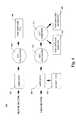
- FIG. 1is an illustration of an error correcting code for 4-bit words in accordance with a basic method of prior art
- FIG. 2is an illustration of an application of a Hamming algorithm in accordance with prior art
- FIG. 3is a flow chart for an exemplary method of recycling ECC, according to an aspect of the present disclosure
- FIG. 4is a flow chart for an exemplary method of recycling ECC, according to an aspect of the present disclosure
- FIG. 5is a chart for an exemplary method of ECC re-use, according to an aspect of the present disclosure.
- FIG. 6is an isometric view of a device and block diagram according to yet one or more aspects of the present disclosure.
- circuit elements or circuit blocksmay be shown or described as multi-conductor or single conductor single lines.
- Each of the multi-conductor signal linesmay alternatively be single conductor signal lines, and each of the single conductor signal lines may alternatively be multi-conductor signal lines.
- Signals and signaling paths shown or described as being single endedmay also be differential, and vice-versa.
- the present disclosureis directed to a variety of error correcting techniques implementing recycled ECC chunk to detect errors in a previously corrected data block.
- NAND Flash devicesoften use a couple of different memory cell technologies.
- One designuses a traditional implementation, wherein each memory cell represents a single bit of data or the SLC approach.
- Another designis to program each cell in incremental amounts. In this approach, how much or how hard a cell is programmed determines the data value of the cell and is called the multi level cell (MLC) approach. With the MLC approach each cell represents 2 bits of data.
- MLCmulti level cell
- SLC NAND Flash devicescan provide improved data integrity when compared with MLC NAND Flash devices because the data integrity in MLC requires more sophisticate error correction scheme than is used for SLC NAND Flash devices.
- the methods for implementation of recycling unused ECC parity bits during flash memory programmingare not limited to any specific type of SLC or MLC Flash device, nor are they limited to any specific error correction scheme.
- Hamming codes illustrated and discussed hereinare meant to demonstrate the method contemplated by the disclosure and not to limit the methods to any one specific device and/or to any one specific error correcting and/or detecting scheme.
- FIG. 1Illustrated in FIG. 1 are conventional Venn diagrams to depict a simple graphical representation of the idea of an error correcting code for four bit words.
- the Venn diagram of FIG. 2-14( a )contains three circles labeled A, B, and C, which combined form seven regions. Regions A, B, and C are the outermost regions and region ABC is the innermost region. AB, AC, and BC each represent the other three regions.
- a 4-bit memory word of 1100is encoded in the regions AB, ABC, AC, and BC, with one bit per region.
- a parity bit to each of the three empty regionsis added to produce an even parity.
- Parity bitsare appended to the data and are chosen so as to have the number of ‘1’ bits in the syndrome or codeword to be even or odd for any particular detection/correction technique. Adding parity bits to make the number of bits a predetermined odd or even number is used for the purpose of identifying whether the bits being transferred from memory arrived successfully. Before the bits are sent, they are counted and if the total number of data bits is even, the parity bit will be set so that the total number of bits will form an odd number. For example, the sum of the bits in each of three circles A, B, and C, is an even number. In circle A of the middle diagram of FIG.
- the third diagram on the far right of FIG. 1illustrates the same bits that have been transferred for a memory operation but arrived with error wherein the AC region has gone bad by changing from a 0 to a 1. Because the count is odd instead of even, the computer can see at the receiving end that circles A and C have the wrong parity, odd instead of the original even. A transmission error has occurred and either transmission is retried, repaired, or the system halts and an error message is sent to the user. The only single bit change that corrects them is to restore AC back to 0.
- a computermay detect and correct single bit errors by using an even or odd parity but this way of checking is not infallible since it is possible to have two bits in error in a transmission, thereby offsetting one another.
- This possibilitynotably is remote in personal computers, however in more complex and denser data systems where reliability and integrity is desired additional bits are allocated of parity checking.
- no paritymay be used where systems, such as modems may not check or transmit parity bits in lieu of other forms of checking errors in transmission.
- the advantage of no parityis that the parity bits can be used for data, and therefore speed up transmission.
- Different algorithmsmay be implemented as various coding schemes such as Hamming code, BCH (Bose, Chaudhuri, Hocquenghem) code, or Reed-Solomon code.
- Hamming codeBCH (Bose, Chaudhuri, Hocquenghem) code
- Reed-Solomon codeFor example, the ECC method using Hamming codes with predetermined bits is able to detect a 2-bit error (i.e., two error bits) and to correct single bit errors.
- a method using Hamming codestherefore functions to detect 2-bit errors and correct a 1-bit error.
- FIG. 2is an illustration of example of how the Hamming algorithm can also be used to construct error correction codes (ECC) for any size memory word.
- ECCerror correction codes
- a new wordis formed in a Hamming code that is a length of x+m bits.
- the bitsare numbered starting at 1, not 0, with the first bit 1 the leftmost, highest order bit. All bits whose bit number is a power of 2 are then parity bits while the rest are used as data bits. For example, with a 16 bit word, 5 parity bits are added when ECC is generated by the Hamming algorithm to comprise a 21 bit word.
- bits 1 , 2 , 4 , 8 , and 16are parity bits in the example of FIG. 2 and the rest are data bits. Even parity is arbitrarily chosen in this example. Therefore, each parity bit checks specific bits positions and is set so that the total number of 1s in the checks positions is even. For example, the bit positions checked by the parity bit 1 checks bits 1 , 3 , 5 , 7 , 9 , 11 , 13 , 15 , 17 , 19 , and 21 .
- Bit 2checks bits 2 , 3 , 6 , 7 , 10 , 11 , 14 , 15 , 18 , and 19 .
- Bit 4checks bits 8 , 9 , 10 , 11 , 12 , 13 , 14 , 15 .
- FIG. 2illustrates a construction of a Hamming code for the 16-bit memory word 1 1 1 1 0 0 0 0 0 1 0 1 1 0 0.
- the 21-bit codeword or syndromeis 0 0 1 0 1 1 1 0 0 0 0 0 0 1 0 1 1 0 1 0 0.
- the new incorrect 21-bit codewordwould be 0 0 1 0 0 1 1 0 0 0 0 0 0 0 1 0 1 1 0 1 1 0 1 1 0 0.
- Parity bit 1 incorrect( 1 , 3 , 5 , 7 , 9 , 11 , 13 , 15 , 17 , 19 , 21 contains five 1s); Parity bit 2 correct ( 2 , 3 , 6 , 7 , 10 , 11 , 14 , 15 , 18 , 19 contains six 1s); parity bit 4 incorrect ( 4 , 5 , 6 , 7 , 12 , 13 , 14 , 15 , containing two 1s). Parity bit 16 correct ( 16 , 17 , 18 , 19 , 20 , 21 contains four 1s). Parity bit 1 and 4 are incorrect because the total number of 1s should be an even number. Either by a process of elimination or adding the incorrect parity bits up will result in the only bit to have an error is bit 5 . Because it was read as a 1 it should be a 0. In this manner, errors can be corrected.
- FIG. 3is illustrated a flowchart of an improved method 300 of one embodiment of the present disclosure.
- ECCis re-encoded based on the most recent data block.
- a data blockmay comprise any user type data combined or not with any stored data of a memory array and ECC.
- ECCerror correcting codes
- codes of block typeand codes of convolutional type. Codes of block type as discussed supra encode a fixed number of bits, for example k bits, into a vector of specific length, n for example.
- the main characterization of a block codeis that it is a fixed length channel code (unlike source coding schemes such as Huffman coding, and unlike channel coding methods like convolutional encoding). Therefore, the information string is divided into blocks of k-bits each. A block code takes a k-digit information word and transforms this into an n-digit codeword.
- the method of FIG. 3demonstrates an ability to re-use ECC when reasonable to do so and inhibit ECC when it no longer serves a strong purpose. For example, if a user inputs any number of bytes, and for a certain amount of bytes (i.e., block of data) an ECC word called a syndrome corresponds to it with about 9 to 24 bits used specifically to do repairs later on.
- an ECC word called a syndromecorresponds to it with about 9 to 24 bits used specifically to do repairs later on.
- Flash memoryonce a bit is programmed or set to a zero, a ‘1’ cannot be written or programmed to it independently without first erasing the entire array sector and then subsequently writing it back. This is a problem in particular when pieces or chunks of data are written at a time.
- ECC parityis encoded from user and core data or stored data according to an ECC syndrome encoder for generating a syndrome from each word to be stored or transmitted through a channel.
- ECC parityis encoded from the user data and core data already stored in the particular memory array.
- Any channelis thought of to be a source of possible error that corrupts the data and ECC parity represented by the syndrome.
- a channelmay be a storage media (e.g., hard disk, optical disk, etc.) or a network connection (e.g., connection with other computers, or a wireless connection such as that used in satellite communications).
- the term channelis used to represent any source of possible error or noise as the case may be that possibly corrupts the codeword or syndrome thereby modifying it.
- an encoder(not shown) generates ECC parity code, for example based on the previously corrected data block. After calculating ECC by any method scheme capable of such calculation, new ECC parity code is generated. The new ECC parity code is encoded based on the existing previous core data and new user data. The generated ECC parity code is then compared to data read from the older core ECC parity to determine which decision is implemented at 306 .
- the old ECCcan be encoded by the new ECC is examined. A decision is made based on whether the old ECC requires a ‘1’ to be programmed over a ‘0’. If the programming involves programming erased data over programmed data, the decision to program the core ECC parity in alignment to the new ECC expected data outputted from an ECC encoder is foregone. Therefore, programming any ECC parity code to the core ECC parity is skipped as demonstrated at 310 of FIG. 3 and that ECC goes abandoned.
- the core ECC parity datais inhibited to prevent subsequent use of the ECC. It is no longer an option for future comparison of any new ECC outputted by an ECC encoder.
- the core ECC parityis therefore labeled as inhibited.
- the programming of an indicator bitactuates this inhibit label.
- the indicator bit programmedis associated to the particular ECC chunk of data and causes the ECC to be rendered abandoned for any subsequent programming.
- the decision at 306determines that data in the core ECC parity compared to the generated ECC parity code was compatible by programming programmed data over erased data (i.e., a ‘1’ data over a ‘0’ data) then the decision flows to 308 to instigate programming the ECC parity code to the core ECC parity since the core ECC parity is able to be recycled.
- the new ECC parity codeis programmed to the core ECC parity.
- Flash memoryoffers a variety of benefits to the end user as discussed supra, employing flash memory also gives rise to several additional problems. Flash memory typically has a long programming and erasing time. The programming of a memory cell can often take milliseconds to reach a required charge level on the floating gate on the transistor. In addition, over-erasing often negatively impacts flash memory because an excessive charge is removed from the floating gate of the memory cell. Corrective programming often has to be employed to mitigate the damage caused by over-erasing.
- FIG. 4is illustrated another embodiment of the present disclosure in a flow diagram.
- a userputs in so many bytes into a blank sector of memory 402 .
- an ECC word or a syndromecorresponds to it with about 9 to 24 bits used to do a repair later on.
- the following chartdepicts the typical number of bits required for repair corresponding to the length of the syndrome:
- the method 400 of the present disclosurebegins at the user data 402 being stored into a blank sector, as illustrated in FIG. 4 .
- ECCis calculated by any means capable of calculating ECC into user information and/or a user data word.
- ECC calculatingmay implement calculating detection and/or correction by any means possible.
- an ECC syndromeis formed.
- the ECC syndrome programmed into the user datais stored. The ECC with corresponding data remains to be used for potential recycling of the same ECC as envisioned by the inventors of the present invention, in addition to any other transmission functions inherent to memory operations involving a channel.
- ECCis calculated by any means capable of calculating ECC into user information and/or a user data word.
- ECC calculatingmay implement calculating detection and/or correction by any means possible.
- ECC comparisonoccurs at 412 wherein the existing ECC codeword or syndrome is compared to the new requested updated data for ECC and determines whether or not ECC can still be supported or not.
- the methodwill compare it to the previous one for that block of data and in some instances advance an update to the ECC code word with the new one. At other times this will not be possible in which case generally the ECC will be disabled.
- the ECC at 416will therein be inhibited in the present method.
- the inhibition processcomprises programming an indicator bit associated to the ECC chunk.
- the core ECC parity datais inhibited to prevent subsequent use of the ECC. It is no longer an option for future comparison of any new ECC outputted by an ECC encoder.
- the core ECC parityis therefore labeled as inhibited wherein the programming of the indicator bit actuates this inhibit label.
- the indicator bit programmedis associated to the particular ECC chunk of data and causes the ECC to be rendered abandoned for any subsequent programming.
- the inhibit bitremoves ECC parity bits from future programs and reads. There continues to be only one ECC word while active and it always represents the sum of data at the current time.
- the ECC methodflows to 418 wherein ECC is not inhibited.
- the user data and new ECCis programmed and reliably secured for transmission or operation.
- the decision at 412determines that data in the core ECC parity compared to the generated ECC parity code was flawed and correction is possible by programming programmed data over erased data (i.e., a ‘1’ data over a ‘0’ data) then the decision flows to 418 to instigate programming the ECC parity code with new data to the core ECC parity.
- the new ECC parity codeis programmed to the core ECC parity.
- ECC parityOne advantage of re-using ECC parity is that extra parity bits are not needed all the time and these bits can be used for data, and therefore speed up transmission. Statistically, the method 400 will get 50% better ECC coverage on the whole than any method without recycle. In alternative methods it is common to loose ECC every time a reprogram occurs, but if not continual support is capable. Prior designs for multiple program, or bit twiddling in NOR structures did not have ECC. Prior methods would limit the size of reprogramming. For example, for NAND program granularity would be limited to match the ECC granularity.
- the ECC sizeis 64 bytes or 256 bytes, for example, a user would be able to reprogram, but limited in manner because not within the same number of bytes.
- the area a user wants to reprogramis generally only 3-4% of the die. Therefore, a user would not have to change his code and still get benefit of that code to the extent that it helps reliability considerably.
- a blank memory sectormay hold 64 bytes.
- an ECC wordwill be calculated into the 32 bytes. For example, if ‘5 5’ gets written into the memory the data bytes for ‘9 9’ get stored into the ECC word chunk and the main data is then stored. Afterwards, when the user programs the upper 32 bytes of data and the flash is full, but when new ECC word chunk is calculated three main actions may occur.
- ECCError Correction Code
- FIG. 5illustrates another embodiment of a method 600 of the present disclosure wherein ECC gets inhibited for re-use at the last program 618 .
- the ECC codewordgets inhibited when a new ECC 612 code bit requires programming from a ‘0’ to a ‘1’ during a new ECC code program 612 to the old or stored ECC code 610 .
- the initial program 614 of user data to a memory arraybegins with data words D 3 602 , D 2 604 , D 1 606 , D 0 608 that in the example illustrated contains words 0xFFFF, 0xFFF, 0x1234, and 0x5678, respectively.
- the ECC already stored 610comprises the parity bit data 0x7F and ECC new 612 contains 0x77. Because the old ECC chunk 610 is compatible with the new ECC 612 chunk then no inhibition at 613 is enabled to prevent correction of the core or stored the ECC. Therefore, when a second program 616 occurs and the word 0x9ABC is programmed into the same block of the same length at D 2 604 then the ECC stored 610 is now the same as the previous ECC new 612 and therein is recalled for comparison between the new ECC 612 for the second program operation 616 .
- the new ECC word 612 expectedis compatible with the old (i.e., a ‘0’ data may be programmed over a ‘1’ data to make the ECC useable in conjunction with the old ECC data 610 ). Therefore, no inhibition occurs at 613 for the second program 616 and recycling of the ECC occurs. However, if in a program operation, for example in the last program 618 of user data, the old ECC 610 is not able to be utilized for re-use and therein the ECC of the stored core gets inhibited and not used in any correction. The inhibition occurs when an attempt is made to write an erased data over a programmed data.
- FIG. 6is an exemplary portable electronic device, for example, a Personal Data Assistant (PDA) 600 comprising a video display 602 , an input component 604 , a housing 606 , a CPU 608 , a transceiver and/or a receiver 610 , a microphone 612 , a power supply 614 , an audio output device 616 , an audio input 618 , flash memory 620 , various sensors 622 , and speaker(s) 624 .
- the flash memory 620utilizing dual bit and single bit memory devices manufactured with improved methods for recycling unused ECC parity bits during flash programming, per the present invention.
- the audio input device 618can be a transducer, for example.
- the input component 604can include a keypad, buttons, dials, pressure keys, and the like.
- the video display 602can be a liquid crystal display, a plasma display, an LED display, and the like, for displaying visual data and information.
- the portable device with flash memory 620 manufactured according to the present inventioncomprises cell phones, memory sticks, flash drive devices, video camcorders, voice recorders, USB flash drives, fax machines, flash memory laptops, MP3 players, digital cameras, home video game consoles, hard drives, memory cards (used as solid-state disks in laptops), and the like.
- the flash memory 620can include random access memory, read only memory, optical memory, audio memory, magnetic memory, and the like.
Landscapes
- Engineering & Computer Science (AREA)
- Theoretical Computer Science (AREA)
- Quality & Reliability (AREA)
- Physics & Mathematics (AREA)
- General Engineering & Computer Science (AREA)
- General Physics & Mathematics (AREA)
- Techniques For Improving Reliability Of Storages (AREA)
Abstract
Description
| Word Size | Check bits | Total | Percent Overhead | ||
| 8 | 4 | 12 | 50 | ||
| 16 | 5 | 21 | 31 | ||
| 32 | 6 | 38 | 19 | ||
| 64 | 7 | 71 | 11 | ||
| 128 | 8 | 136 | 6 | ||
| 256 | 9 | 265 | 4 | ||
| 512 | 10 | 522 | 2 | ||
Claims (20)
Priority Applications (1)
| Application Number | Priority Date | Filing Date | Title |
|---|---|---|---|
| US12/198,381US8117521B2 (en) | 2008-08-26 | 2008-08-26 | Implementation of recycling unused ECC parity bits during flash memory programming |
Applications Claiming Priority (1)
| Application Number | Priority Date | Filing Date | Title |
|---|---|---|---|
| US12/198,381US8117521B2 (en) | 2008-08-26 | 2008-08-26 | Implementation of recycling unused ECC parity bits during flash memory programming |
Publications (2)
| Publication Number | Publication Date |
|---|---|
| US20100058151A1 US20100058151A1 (en) | 2010-03-04 |
| US8117521B2true US8117521B2 (en) | 2012-02-14 |
Family
ID=41727093
Family Applications (1)
| Application Number | Title | Priority Date | Filing Date |
|---|---|---|---|
| US12/198,381Active2030-12-15US8117521B2 (en) | 2008-08-26 | 2008-08-26 | Implementation of recycling unused ECC parity bits during flash memory programming |
Country Status (1)
| Country | Link |
|---|---|
| US (1) | US8117521B2 (en) |
Cited By (124)
| Publication number | Priority date | Publication date | Assignee | Title |
|---|---|---|---|---|
| US20130339822A1 (en)* | 2012-06-15 | 2013-12-19 | International Business Machines Corporation | Bad wordline/array detection in memory |
| US9535787B2 (en) | 2015-02-12 | 2017-01-03 | International Business Machines Corporation | Dynamic cache row fail accumulation due to catastrophic failure |
| TWI575529B (en)* | 2015-01-29 | 2017-03-21 | 華邦電子股份有限公司 | Method of enhancing error correction in data storage system and data storage system thereof |
| US10817431B2 (en) | 2014-07-02 | 2020-10-27 | Pure Storage, Inc. | Distributed storage addressing |
| US10838633B2 (en) | 2014-06-04 | 2020-11-17 | Pure Storage, Inc. | Configurable hyperconverged multi-tenant storage system |
| US10942869B2 (en) | 2017-03-30 | 2021-03-09 | Pure Storage, Inc. | Efficient coding in a storage system |
| US11030090B2 (en) | 2016-07-26 | 2021-06-08 | Pure Storage, Inc. | Adaptive data migration |
| US11074016B2 (en) | 2017-10-31 | 2021-07-27 | Pure Storage, Inc. | Using flash storage devices with different sized erase blocks |
| US11079962B2 (en) | 2014-07-02 | 2021-08-03 | Pure Storage, Inc. | Addressable non-volatile random access memory |
| US11086532B2 (en) | 2017-10-31 | 2021-08-10 | Pure Storage, Inc. | Data rebuild with changing erase block sizes |
| US11138082B2 (en) | 2014-06-04 | 2021-10-05 | Pure Storage, Inc. | Action determination based on redundancy level |
| US11144212B2 (en) | 2015-04-10 | 2021-10-12 | Pure Storage, Inc. | Independent partitions within an array |
| US11190580B2 (en) | 2017-07-03 | 2021-11-30 | Pure Storage, Inc. | Stateful connection resets |
| US11188476B1 (en) | 2014-08-20 | 2021-11-30 | Pure Storage, Inc. | Virtual addressing in a storage system |
| US11204830B2 (en) | 2014-08-07 | 2021-12-21 | Pure Storage, Inc. | Die-level monitoring in a storage cluster |
| US11204701B2 (en) | 2015-12-22 | 2021-12-21 | Pure Storage, Inc. | Token based transactions |
| US11240307B2 (en) | 2015-04-09 | 2022-02-01 | Pure Storage, Inc. | Multiple communication paths in a storage system |
| US11289169B2 (en) | 2017-01-13 | 2022-03-29 | Pure Storage, Inc. | Cycled background reads |
| US11310317B1 (en) | 2014-06-04 | 2022-04-19 | Pure Storage, Inc. | Efficient load balancing |
| US11307998B2 (en) | 2017-01-09 | 2022-04-19 | Pure Storage, Inc. | Storage efficiency of encrypted host system data |
| US11334254B2 (en) | 2019-03-29 | 2022-05-17 | Pure Storage, Inc. | Reliability based flash page sizing |
| US11340821B2 (en) | 2016-07-26 | 2022-05-24 | Pure Storage, Inc. | Adjustable migration utilization |
| US11354058B2 (en) | 2018-09-06 | 2022-06-07 | Pure Storage, Inc. | Local relocation of data stored at a storage device of a storage system |
| US11385799B2 (en) | 2014-06-04 | 2022-07-12 | Pure Storage, Inc. | Storage nodes supporting multiple erasure coding schemes |
| US11385979B2 (en) | 2014-07-02 | 2022-07-12 | Pure Storage, Inc. | Mirrored remote procedure call cache |
| US11392522B2 (en) | 2014-07-03 | 2022-07-19 | Pure Storage, Inc. | Transfer of segmented data |
| US11409437B2 (en) | 2016-07-22 | 2022-08-09 | Pure Storage, Inc. | Persisting configuration information |
| US11416144B2 (en) | 2019-12-12 | 2022-08-16 | Pure Storage, Inc. | Dynamic use of segment or zone power loss protection in a flash device |
| US11442645B2 (en) | 2018-01-31 | 2022-09-13 | Pure Storage, Inc. | Distributed storage system expansion mechanism |
| US11442625B2 (en) | 2014-08-07 | 2022-09-13 | Pure Storage, Inc. | Multiple read data paths in a storage system |
| US11489668B2 (en) | 2015-09-30 | 2022-11-01 | Pure Storage, Inc. | Secret regeneration in a storage system |
| US11494498B2 (en) | 2014-07-03 | 2022-11-08 | Pure Storage, Inc. | Storage data decryption |
| US11507597B2 (en) | 2021-03-31 | 2022-11-22 | Pure Storage, Inc. | Data replication to meet a recovery point objective |
| US11544143B2 (en) | 2014-08-07 | 2023-01-03 | Pure Storage, Inc. | Increased data reliability |
| US11550473B2 (en) | 2016-05-03 | 2023-01-10 | Pure Storage, Inc. | High-availability storage array |
| US11550752B2 (en) | 2014-07-03 | 2023-01-10 | Pure Storage, Inc. | Administrative actions via a reserved filename |
| US11567917B2 (en) | 2015-09-30 | 2023-01-31 | Pure Storage, Inc. | Writing data and metadata into storage |
| US11582046B2 (en) | 2015-10-23 | 2023-02-14 | Pure Storage, Inc. | Storage system communication |
| US11592985B2 (en) | 2017-04-05 | 2023-02-28 | Pure Storage, Inc. | Mapping LUNs in a storage memory |
| US11593203B2 (en) | 2014-06-04 | 2023-02-28 | Pure Storage, Inc. | Coexisting differing erasure codes |
| US11604690B2 (en) | 2016-07-24 | 2023-03-14 | Pure Storage, Inc. | Online failure span determination |
| US11604598B2 (en) | 2014-07-02 | 2023-03-14 | Pure Storage, Inc. | Storage cluster with zoned drives |
| US11614880B2 (en) | 2020-12-31 | 2023-03-28 | Pure Storage, Inc. | Storage system with selectable write paths |
| US11620197B2 (en) | 2014-08-07 | 2023-04-04 | Pure Storage, Inc. | Recovering error corrected data |
| US11652884B2 (en) | 2014-06-04 | 2023-05-16 | Pure Storage, Inc. | Customized hash algorithms |
| US11650976B2 (en) | 2011-10-14 | 2023-05-16 | Pure Storage, Inc. | Pattern matching using hash tables in storage system |
| US11656768B2 (en) | 2016-09-15 | 2023-05-23 | Pure Storage, Inc. | File deletion in a distributed system |
| US11675762B2 (en) | 2015-06-26 | 2023-06-13 | Pure Storage, Inc. | Data structures for key management |
| US11704192B2 (en) | 2019-12-12 | 2023-07-18 | Pure Storage, Inc. | Budgeting open blocks based on power loss protection |
| US11704073B2 (en) | 2015-07-13 | 2023-07-18 | Pure Storage, Inc | Ownership determination for accessing a file |
| US11714708B2 (en) | 2017-07-31 | 2023-08-01 | Pure Storage, Inc. | Intra-device redundancy scheme |
| US11722455B2 (en) | 2017-04-27 | 2023-08-08 | Pure Storage, Inc. | Storage cluster address resolution |
| US11734169B2 (en) | 2016-07-26 | 2023-08-22 | Pure Storage, Inc. | Optimizing spool and memory space management |
| US11740909B2 (en) | 2021-11-09 | 2023-08-29 | Meta Platforms, Inc. | Secure speculative execution of instructions |
| US11740802B2 (en) | 2015-09-01 | 2023-08-29 | Pure Storage, Inc. | Error correction bypass for erased pages |
| US11741003B2 (en) | 2017-11-17 | 2023-08-29 | Pure Storage, Inc. | Write granularity for storage system |
| US11775428B2 (en) | 2015-03-26 | 2023-10-03 | Pure Storage, Inc. | Deletion immunity for unreferenced data |
| US11775491B2 (en) | 2020-04-24 | 2023-10-03 | Pure Storage, Inc. | Machine learning model for storage system |
| US11782625B2 (en) | 2017-06-11 | 2023-10-10 | Pure Storage, Inc. | Heterogeneity supportive resiliency groups |
| US11789626B2 (en) | 2020-12-17 | 2023-10-17 | Pure Storage, Inc. | Optimizing block allocation in a data storage system |
| US11797212B2 (en) | 2016-07-26 | 2023-10-24 | Pure Storage, Inc. | Data migration for zoned drives |
| US11822807B2 (en) | 2019-06-24 | 2023-11-21 | Pure Storage, Inc. | Data replication in a storage system |
| US11822444B2 (en) | 2014-06-04 | 2023-11-21 | Pure Storage, Inc. | Data rebuild independent of error detection |
| US11836348B2 (en) | 2018-04-27 | 2023-12-05 | Pure Storage, Inc. | Upgrade for system with differing capacities |
| US11842053B2 (en) | 2016-12-19 | 2023-12-12 | Pure Storage, Inc. | Zone namespace |
| US11847324B2 (en) | 2020-12-31 | 2023-12-19 | Pure Storage, Inc. | Optimizing resiliency groups for data regions of a storage system |
| US11847013B2 (en) | 2018-02-18 | 2023-12-19 | Pure Storage, Inc. | Readable data determination |
| US11846968B2 (en) | 2018-09-06 | 2023-12-19 | Pure Storage, Inc. | Relocation of data for heterogeneous storage systems |
| US11847331B2 (en) | 2019-12-12 | 2023-12-19 | Pure Storage, Inc. | Budgeting open blocks of a storage unit based on power loss prevention |
| US11861188B2 (en) | 2016-07-19 | 2024-01-02 | Pure Storage, Inc. | System having modular accelerators |
| US11868309B2 (en) | 2018-09-06 | 2024-01-09 | Pure Storage, Inc. | Queue management for data relocation |
| US11869583B2 (en) | 2017-04-27 | 2024-01-09 | Pure Storage, Inc. | Page write requirements for differing types of flash memory |
| US11886288B2 (en) | 2016-07-22 | 2024-01-30 | Pure Storage, Inc. | Optimize data protection layouts based on distributed flash wear leveling |
| US11886308B2 (en) | 2014-07-02 | 2024-01-30 | Pure Storage, Inc. | Dual class of service for unified file and object messaging |
| US11886334B2 (en) | 2016-07-26 | 2024-01-30 | Pure Storage, Inc. | Optimizing spool and memory space management |
| US11893023B2 (en) | 2015-09-04 | 2024-02-06 | Pure Storage, Inc. | Deterministic searching using compressed indexes |
| US11893126B2 (en) | 2019-10-14 | 2024-02-06 | Pure Storage, Inc. | Data deletion for a multi-tenant environment |
| US11899582B2 (en) | 2019-04-12 | 2024-02-13 | Pure Storage, Inc. | Efficient memory dump |
| US11922070B2 (en) | 2016-10-04 | 2024-03-05 | Pure Storage, Inc. | Granting access to a storage device based on reservations |
| US11955187B2 (en) | 2017-01-13 | 2024-04-09 | Pure Storage, Inc. | Refresh of differing capacity NAND |
| US11960371B2 (en) | 2014-06-04 | 2024-04-16 | Pure Storage, Inc. | Message persistence in a zoned system |
| US11966841B2 (en) | 2018-01-31 | 2024-04-23 | Pure Storage, Inc. | Search acceleration for artificial intelligence |
| US11971828B2 (en) | 2015-09-30 | 2024-04-30 | Pure Storage, Inc. | Logic module for use with encoded instructions |
| US11995318B2 (en) | 2016-10-28 | 2024-05-28 | Pure Storage, Inc. | Deallocated block determination |
| US12001700B2 (en) | 2018-10-26 | 2024-06-04 | Pure Storage, Inc. | Dynamically selecting segment heights in a heterogeneous RAID group |
| US12032724B2 (en) | 2017-08-31 | 2024-07-09 | Pure Storage, Inc. | Encryption in a storage array |
| US12038927B2 (en) | 2015-09-04 | 2024-07-16 | Pure Storage, Inc. | Storage system having multiple tables for efficient searching |
| US12046292B2 (en) | 2017-10-31 | 2024-07-23 | Pure Storage, Inc. | Erase blocks having differing sizes |
| US12050774B2 (en) | 2015-05-27 | 2024-07-30 | Pure Storage, Inc. | Parallel update for a distributed system |
| US12056365B2 (en) | 2020-04-24 | 2024-08-06 | Pure Storage, Inc. | Resiliency for a storage system |
| US12061814B2 (en) | 2021-01-25 | 2024-08-13 | Pure Storage, Inc. | Using data similarity to select segments for garbage collection |
| US12067274B2 (en) | 2018-09-06 | 2024-08-20 | Pure Storage, Inc. | Writing segments and erase blocks based on ordering |
| US12067282B2 (en) | 2020-12-31 | 2024-08-20 | Pure Storage, Inc. | Write path selection |
| US12079125B2 (en) | 2019-06-05 | 2024-09-03 | Pure Storage, Inc. | Tiered caching of data in a storage system |
| US12079494B2 (en) | 2018-04-27 | 2024-09-03 | Pure Storage, Inc. | Optimizing storage system upgrades to preserve resources |
| US12086472B2 (en) | 2015-03-27 | 2024-09-10 | Pure Storage, Inc. | Heterogeneous storage arrays |
| US12093545B2 (en) | 2020-12-31 | 2024-09-17 | Pure Storage, Inc. | Storage system with selectable write modes |
| US12105620B2 (en) | 2016-10-04 | 2024-10-01 | Pure Storage, Inc. | Storage system buffering |
| US12135878B2 (en) | 2019-01-23 | 2024-11-05 | Pure Storage, Inc. | Programming frequently read data to low latency portions of a solid-state storage array |
| US12137140B2 (en) | 2014-06-04 | 2024-11-05 | Pure Storage, Inc. | Scale out storage platform having active failover |
| US12141118B2 (en) | 2016-10-04 | 2024-11-12 | Pure Storage, Inc. | Optimizing storage system performance using data characteristics |
| US12158814B2 (en) | 2014-08-07 | 2024-12-03 | Pure Storage, Inc. | Granular voltage tuning |
| US12182044B2 (en) | 2014-07-03 | 2024-12-31 | Pure Storage, Inc. | Data storage in a zone drive |
| US12197390B2 (en) | 2017-11-20 | 2025-01-14 | Pure Storage, Inc. | Locks in a distributed file system |
| US12204768B2 (en) | 2019-12-03 | 2025-01-21 | Pure Storage, Inc. | Allocation of blocks based on power loss protection |
| US12204413B2 (en) | 2017-06-07 | 2025-01-21 | Pure Storage, Inc. | Snapshot commitment in a distributed system |
| US12204788B1 (en) | 2023-07-21 | 2025-01-21 | Pure Storage, Inc. | Dynamic plane selection in data storage system |
| US12212624B2 (en) | 2014-06-04 | 2025-01-28 | Pure Storage, Inc. | Independent communication pathways |
| US12216903B2 (en) | 2016-10-31 | 2025-02-04 | Pure Storage, Inc. | Storage node data placement utilizing similarity |
| US12229437B2 (en) | 2020-12-31 | 2025-02-18 | Pure Storage, Inc. | Dynamic buffer for storage system |
| US12235743B2 (en) | 2016-06-03 | 2025-02-25 | Pure Storage, Inc. | Efficient partitioning for storage system resiliency groups |
| US12242425B2 (en) | 2017-10-04 | 2025-03-04 | Pure Storage, Inc. | Similarity data for reduced data usage |
| US12271359B2 (en) | 2015-09-30 | 2025-04-08 | Pure Storage, Inc. | Device host operations in a storage system |
| US12282799B2 (en) | 2015-05-19 | 2025-04-22 | Pure Storage, Inc. | Maintaining coherency in a distributed system |
| US12314163B2 (en) | 2022-04-21 | 2025-05-27 | Pure Storage, Inc. | Die-aware scheduler |
| US12314170B2 (en) | 2020-07-08 | 2025-05-27 | Pure Storage, Inc. | Guaranteeing physical deletion of data in a storage system |
| US12341848B2 (en) | 2014-06-04 | 2025-06-24 | Pure Storage, Inc. | Distributed protocol endpoint services for data storage systems |
| US12340107B2 (en) | 2016-05-02 | 2025-06-24 | Pure Storage, Inc. | Deduplication selection and optimization |
| US12373340B2 (en) | 2019-04-03 | 2025-07-29 | Pure Storage, Inc. | Intelligent subsegment formation in a heterogeneous storage system |
| US12379854B2 (en) | 2015-04-10 | 2025-08-05 | Pure Storage, Inc. | Two or more logical arrays having zoned drives |
| US12393340B2 (en) | 2019-01-16 | 2025-08-19 | Pure Storage, Inc. | Latency reduction of flash-based devices using programming interrupts |
| US12430053B2 (en) | 2021-03-12 | 2025-09-30 | Pure Storage, Inc. | Data block allocation for storage system |
| US12430059B2 (en) | 2020-04-15 | 2025-09-30 | Pure Storage, Inc. | Tuning storage devices |
| US12439544B2 (en) | 2022-04-20 | 2025-10-07 | Pure Storage, Inc. | Retractable pivoting trap door |
Families Citing this family (8)
| Publication number | Priority date | Publication date | Assignee | Title |
|---|---|---|---|---|
| EP1460765A1 (en)* | 2003-03-19 | 2004-09-22 | STMicroelectronics S.r.l. | Method for performing error corrections of digital information codified as a symbol sequence |
| US8209578B2 (en)* | 2008-03-11 | 2012-06-26 | Hitachi Global Storage Technologies Netherlands, B.V. | Systems using low density parity check codes for correcting errors |
| TWI456579B (en)* | 2010-03-26 | 2014-10-11 | Silicon Motion Inc | Method for enhancing error correction capability, and associated memory device and controller thereof |
| US20140075094A1 (en)* | 2012-09-12 | 2014-03-13 | GM Global Technology Operations LLC | Method to implement a binary flag in flash memory |
| US20170046224A1 (en)* | 2014-04-25 | 2017-02-16 | Empire Technology Development Llc | Storing data in storage devices |
| US10735030B2 (en)* | 2017-08-07 | 2020-08-04 | Hewlett Packard Enterprise Development Lp | Re-encoding data associated with failed memory devices |
| US11327836B1 (en) | 2020-09-29 | 2022-05-10 | Xilinx, Inc. | Protection of data on a data path in a memory system |
| WO2023047149A1 (en)* | 2021-09-23 | 2023-03-30 | Micron Technology, Inc. | Improved ecc configuration in memories |
Citations (3)
| Publication number | Priority date | Publication date | Assignee | Title |
|---|---|---|---|---|
| US5889792A (en) | 1996-10-01 | 1999-03-30 | Intel Corporation | Method and apparatus for generating syndromes associated with a block of data that employs re-encoding the block of data |
| US6526537B2 (en) | 1997-09-29 | 2003-02-25 | Nec Corporation | Storage for generating ECC and adding ECC to data |
| US20090187803A1 (en)* | 2008-01-21 | 2009-07-23 | Anobit Technologies Ltd. | Decoding of error correction code using partial bit inversion |
- 2008
- 2008-08-26USUS12/198,381patent/US8117521B2/enactiveActive
Patent Citations (3)
| Publication number | Priority date | Publication date | Assignee | Title |
|---|---|---|---|---|
| US5889792A (en) | 1996-10-01 | 1999-03-30 | Intel Corporation | Method and apparatus for generating syndromes associated with a block of data that employs re-encoding the block of data |
| US6526537B2 (en) | 1997-09-29 | 2003-02-25 | Nec Corporation | Storage for generating ECC and adding ECC to data |
| US20090187803A1 (en)* | 2008-01-21 | 2009-07-23 | Anobit Technologies Ltd. | Decoding of error correction code using partial bit inversion |
Cited By (170)
| Publication number | Priority date | Publication date | Assignee | Title |
|---|---|---|---|---|
| US12277106B2 (en) | 2011-10-14 | 2025-04-15 | Pure Storage, Inc. | Flash system having multiple fingerprint tables |
| US11650976B2 (en) | 2011-10-14 | 2023-05-16 | Pure Storage, Inc. | Pattern matching using hash tables in storage system |
| US20130339822A1 (en)* | 2012-06-15 | 2013-12-19 | International Business Machines Corporation | Bad wordline/array detection in memory |
| US8914708B2 (en)* | 2012-06-15 | 2014-12-16 | International Business Machines Corporation | Bad wordline/array detection in memory |
| US9065481B2 (en) | 2012-06-15 | 2015-06-23 | International Business Machines Corporation | Bad wordline/array detection in memory |
| US12137140B2 (en) | 2014-06-04 | 2024-11-05 | Pure Storage, Inc. | Scale out storage platform having active failover |
| US11593203B2 (en) | 2014-06-04 | 2023-02-28 | Pure Storage, Inc. | Coexisting differing erasure codes |
| US11500552B2 (en) | 2014-06-04 | 2022-11-15 | Pure Storage, Inc. | Configurable hyperconverged multi-tenant storage system |
| US12212624B2 (en) | 2014-06-04 | 2025-01-28 | Pure Storage, Inc. | Independent communication pathways |
| US11960371B2 (en) | 2014-06-04 | 2024-04-16 | Pure Storage, Inc. | Message persistence in a zoned system |
| US12141449B2 (en) | 2014-06-04 | 2024-11-12 | Pure Storage, Inc. | Distribution of resources for a storage system |
| US11652884B2 (en) | 2014-06-04 | 2023-05-16 | Pure Storage, Inc. | Customized hash algorithms |
| US11138082B2 (en) | 2014-06-04 | 2021-10-05 | Pure Storage, Inc. | Action determination based on redundancy level |
| US12066895B2 (en) | 2014-06-04 | 2024-08-20 | Pure Storage, Inc. | Heterogenous memory accommodating multiple erasure codes |
| US11822444B2 (en) | 2014-06-04 | 2023-11-21 | Pure Storage, Inc. | Data rebuild independent of error detection |
| US10838633B2 (en) | 2014-06-04 | 2020-11-17 | Pure Storage, Inc. | Configurable hyperconverged multi-tenant storage system |
| US11385799B2 (en) | 2014-06-04 | 2022-07-12 | Pure Storage, Inc. | Storage nodes supporting multiple erasure coding schemes |
| US12101379B2 (en) | 2014-06-04 | 2024-09-24 | Pure Storage, Inc. | Multilevel load balancing |
| US11671496B2 (en) | 2014-06-04 | 2023-06-06 | Pure Storage, Inc. | Load balacing for distibuted computing |
| US12341848B2 (en) | 2014-06-04 | 2025-06-24 | Pure Storage, Inc. | Distributed protocol endpoint services for data storage systems |
| US11310317B1 (en) | 2014-06-04 | 2022-04-19 | Pure Storage, Inc. | Efficient load balancing |
| US11604598B2 (en) | 2014-07-02 | 2023-03-14 | Pure Storage, Inc. | Storage cluster with zoned drives |
| US10817431B2 (en) | 2014-07-02 | 2020-10-27 | Pure Storage, Inc. | Distributed storage addressing |
| US12135654B2 (en) | 2014-07-02 | 2024-11-05 | Pure Storage, Inc. | Distributed storage system |
| US11922046B2 (en) | 2014-07-02 | 2024-03-05 | Pure Storage, Inc. | Erasure coded data within zoned drives |
| US11385979B2 (en) | 2014-07-02 | 2022-07-12 | Pure Storage, Inc. | Mirrored remote procedure call cache |
| US11079962B2 (en) | 2014-07-02 | 2021-08-03 | Pure Storage, Inc. | Addressable non-volatile random access memory |
| US11886308B2 (en) | 2014-07-02 | 2024-01-30 | Pure Storage, Inc. | Dual class of service for unified file and object messaging |
| US11494498B2 (en) | 2014-07-03 | 2022-11-08 | Pure Storage, Inc. | Storage data decryption |
| US11392522B2 (en) | 2014-07-03 | 2022-07-19 | Pure Storage, Inc. | Transfer of segmented data |
| US11550752B2 (en) | 2014-07-03 | 2023-01-10 | Pure Storage, Inc. | Administrative actions via a reserved filename |
| US12182044B2 (en) | 2014-07-03 | 2024-12-31 | Pure Storage, Inc. | Data storage in a zone drive |
| US11928076B2 (en) | 2014-07-03 | 2024-03-12 | Pure Storage, Inc. | Actions for reserved filenames |
| US11204830B2 (en) | 2014-08-07 | 2021-12-21 | Pure Storage, Inc. | Die-level monitoring in a storage cluster |
| US12229402B2 (en) | 2014-08-07 | 2025-02-18 | Pure Storage, Inc. | Intelligent operation scheduling based on latency of operations |
| US12271264B2 (en) | 2014-08-07 | 2025-04-08 | Pure Storage, Inc. | Adjusting a variable parameter to increase reliability of stored data |
| US11544143B2 (en) | 2014-08-07 | 2023-01-03 | Pure Storage, Inc. | Increased data reliability |
| US11442625B2 (en) | 2014-08-07 | 2022-09-13 | Pure Storage, Inc. | Multiple read data paths in a storage system |
| US12373289B2 (en) | 2014-08-07 | 2025-07-29 | Pure Storage, Inc. | Error correction incident tracking |
| US11620197B2 (en) | 2014-08-07 | 2023-04-04 | Pure Storage, Inc. | Recovering error corrected data |
| US12158814B2 (en) | 2014-08-07 | 2024-12-03 | Pure Storage, Inc. | Granular voltage tuning |
| US12253922B2 (en) | 2014-08-07 | 2025-03-18 | Pure Storage, Inc. | Data rebuild based on solid state memory characteristics |
| US11656939B2 (en) | 2014-08-07 | 2023-05-23 | Pure Storage, Inc. | Storage cluster memory characterization |
| US12314131B2 (en) | 2014-08-07 | 2025-05-27 | Pure Storage, Inc. | Wear levelling for differing memory types |
| US12314183B2 (en) | 2014-08-20 | 2025-05-27 | Pure Storage, Inc. | Preserved addressing for replaceable resources |
| US11188476B1 (en) | 2014-08-20 | 2021-11-30 | Pure Storage, Inc. | Virtual addressing in a storage system |
| US11734186B2 (en) | 2014-08-20 | 2023-08-22 | Pure Storage, Inc. | Heterogeneous storage with preserved addressing |
| TWI575529B (en)* | 2015-01-29 | 2017-03-21 | 華邦電子股份有限公司 | Method of enhancing error correction in data storage system and data storage system thereof |
| US9535787B2 (en) | 2015-02-12 | 2017-01-03 | International Business Machines Corporation | Dynamic cache row fail accumulation due to catastrophic failure |
| US12253941B2 (en) | 2015-03-26 | 2025-03-18 | Pure Storage, Inc. | Management of repeatedly seen data |
| US11775428B2 (en) | 2015-03-26 | 2023-10-03 | Pure Storage, Inc. | Deletion immunity for unreferenced data |
| US12086472B2 (en) | 2015-03-27 | 2024-09-10 | Pure Storage, Inc. | Heterogeneous storage arrays |
| US12069133B2 (en) | 2015-04-09 | 2024-08-20 | Pure Storage, Inc. | Communication paths for differing types of solid state storage devices |
| US11240307B2 (en) | 2015-04-09 | 2022-02-01 | Pure Storage, Inc. | Multiple communication paths in a storage system |
| US11722567B2 (en) | 2015-04-09 | 2023-08-08 | Pure Storage, Inc. | Communication paths for storage devices having differing capacities |
| US12379854B2 (en) | 2015-04-10 | 2025-08-05 | Pure Storage, Inc. | Two or more logical arrays having zoned drives |
| US11144212B2 (en) | 2015-04-10 | 2021-10-12 | Pure Storage, Inc. | Independent partitions within an array |
| US12282799B2 (en) | 2015-05-19 | 2025-04-22 | Pure Storage, Inc. | Maintaining coherency in a distributed system |
| US12050774B2 (en) | 2015-05-27 | 2024-07-30 | Pure Storage, Inc. | Parallel update for a distributed system |
| US11675762B2 (en) | 2015-06-26 | 2023-06-13 | Pure Storage, Inc. | Data structures for key management |
| US12093236B2 (en) | 2015-06-26 | 2024-09-17 | Pure Storage, Inc. | Probalistic data structure for key management |
| US12147715B2 (en) | 2015-07-13 | 2024-11-19 | Pure Storage, Inc. | File ownership in a distributed system |
| US11704073B2 (en) | 2015-07-13 | 2023-07-18 | Pure Storage, Inc | Ownership determination for accessing a file |
| US11740802B2 (en) | 2015-09-01 | 2023-08-29 | Pure Storage, Inc. | Error correction bypass for erased pages |
| US11893023B2 (en) | 2015-09-04 | 2024-02-06 | Pure Storage, Inc. | Deterministic searching using compressed indexes |
| US12038927B2 (en) | 2015-09-04 | 2024-07-16 | Pure Storage, Inc. | Storage system having multiple tables for efficient searching |
| US12072860B2 (en) | 2015-09-30 | 2024-08-27 | Pure Storage, Inc. | Delegation of data ownership |
| US11971828B2 (en) | 2015-09-30 | 2024-04-30 | Pure Storage, Inc. | Logic module for use with encoded instructions |
| US11489668B2 (en) | 2015-09-30 | 2022-11-01 | Pure Storage, Inc. | Secret regeneration in a storage system |
| US11567917B2 (en) | 2015-09-30 | 2023-01-31 | Pure Storage, Inc. | Writing data and metadata into storage |
| US11838412B2 (en) | 2015-09-30 | 2023-12-05 | Pure Storage, Inc. | Secret regeneration from distributed shares |
| US12271359B2 (en) | 2015-09-30 | 2025-04-08 | Pure Storage, Inc. | Device host operations in a storage system |
| US11582046B2 (en) | 2015-10-23 | 2023-02-14 | Pure Storage, Inc. | Storage system communication |
| US11204701B2 (en) | 2015-12-22 | 2021-12-21 | Pure Storage, Inc. | Token based transactions |
| US12067260B2 (en) | 2015-12-22 | 2024-08-20 | Pure Storage, Inc. | Transaction processing with differing capacity storage |
| US12340107B2 (en) | 2016-05-02 | 2025-06-24 | Pure Storage, Inc. | Deduplication selection and optimization |
| US11847320B2 (en) | 2016-05-03 | 2023-12-19 | Pure Storage, Inc. | Reassignment of requests for high availability |
| US11550473B2 (en) | 2016-05-03 | 2023-01-10 | Pure Storage, Inc. | High-availability storage array |
| US12235743B2 (en) | 2016-06-03 | 2025-02-25 | Pure Storage, Inc. | Efficient partitioning for storage system resiliency groups |
| US11861188B2 (en) | 2016-07-19 | 2024-01-02 | Pure Storage, Inc. | System having modular accelerators |
| US11409437B2 (en) | 2016-07-22 | 2022-08-09 | Pure Storage, Inc. | Persisting configuration information |
| US11886288B2 (en) | 2016-07-22 | 2024-01-30 | Pure Storage, Inc. | Optimize data protection layouts based on distributed flash wear leveling |
| US12105584B2 (en) | 2016-07-24 | 2024-10-01 | Pure Storage, Inc. | Acquiring failure information |
| US11604690B2 (en) | 2016-07-24 | 2023-03-14 | Pure Storage, Inc. | Online failure span determination |
| US11886334B2 (en) | 2016-07-26 | 2024-01-30 | Pure Storage, Inc. | Optimizing spool and memory space management |
| US11734169B2 (en) | 2016-07-26 | 2023-08-22 | Pure Storage, Inc. | Optimizing spool and memory space management |
| US11030090B2 (en) | 2016-07-26 | 2021-06-08 | Pure Storage, Inc. | Adaptive data migration |
| US11340821B2 (en) | 2016-07-26 | 2022-05-24 | Pure Storage, Inc. | Adjustable migration utilization |
| US11797212B2 (en) | 2016-07-26 | 2023-10-24 | Pure Storage, Inc. | Data migration for zoned drives |
| US11656768B2 (en) | 2016-09-15 | 2023-05-23 | Pure Storage, Inc. | File deletion in a distributed system |
| US12393353B2 (en) | 2016-09-15 | 2025-08-19 | Pure Storage, Inc. | Storage system with distributed deletion |
| US11922033B2 (en) | 2016-09-15 | 2024-03-05 | Pure Storage, Inc. | Batch data deletion |
| US12105620B2 (en) | 2016-10-04 | 2024-10-01 | Pure Storage, Inc. | Storage system buffering |
| US12141118B2 (en) | 2016-10-04 | 2024-11-12 | Pure Storage, Inc. | Optimizing storage system performance using data characteristics |
| US11922070B2 (en) | 2016-10-04 | 2024-03-05 | Pure Storage, Inc. | Granting access to a storage device based on reservations |
| US11995318B2 (en) | 2016-10-28 | 2024-05-28 | Pure Storage, Inc. | Deallocated block determination |
| US12216903B2 (en) | 2016-10-31 | 2025-02-04 | Pure Storage, Inc. | Storage node data placement utilizing similarity |
| US11842053B2 (en) | 2016-12-19 | 2023-12-12 | Pure Storage, Inc. | Zone namespace |
| US11762781B2 (en) | 2017-01-09 | 2023-09-19 | Pure Storage, Inc. | Providing end-to-end encryption for data stored in a storage system |
| US11307998B2 (en) | 2017-01-09 | 2022-04-19 | Pure Storage, Inc. | Storage efficiency of encrypted host system data |
| US11955187B2 (en) | 2017-01-13 | 2024-04-09 | Pure Storage, Inc. | Refresh of differing capacity NAND |
| US11289169B2 (en) | 2017-01-13 | 2022-03-29 | Pure Storage, Inc. | Cycled background reads |
| US10942869B2 (en) | 2017-03-30 | 2021-03-09 | Pure Storage, Inc. | Efficient coding in a storage system |
| US11592985B2 (en) | 2017-04-05 | 2023-02-28 | Pure Storage, Inc. | Mapping LUNs in a storage memory |
| US11869583B2 (en) | 2017-04-27 | 2024-01-09 | Pure Storage, Inc. | Page write requirements for differing types of flash memory |
| US11722455B2 (en) | 2017-04-27 | 2023-08-08 | Pure Storage, Inc. | Storage cluster address resolution |
| US12204413B2 (en) | 2017-06-07 | 2025-01-21 | Pure Storage, Inc. | Snapshot commitment in a distributed system |
| US11782625B2 (en) | 2017-06-11 | 2023-10-10 | Pure Storage, Inc. | Heterogeneity supportive resiliency groups |
| US11190580B2 (en) | 2017-07-03 | 2021-11-30 | Pure Storage, Inc. | Stateful connection resets |
| US11689610B2 (en) | 2017-07-03 | 2023-06-27 | Pure Storage, Inc. | Load balancing reset packets |
| US12086029B2 (en) | 2017-07-31 | 2024-09-10 | Pure Storage, Inc. | Intra-device and inter-device data recovery in a storage system |
| US11714708B2 (en) | 2017-07-31 | 2023-08-01 | Pure Storage, Inc. | Intra-device redundancy scheme |
| US12032724B2 (en) | 2017-08-31 | 2024-07-09 | Pure Storage, Inc. | Encryption in a storage array |
| US12242425B2 (en) | 2017-10-04 | 2025-03-04 | Pure Storage, Inc. | Similarity data for reduced data usage |
| US12293111B2 (en) | 2017-10-31 | 2025-05-06 | Pure Storage, Inc. | Pattern forming for heterogeneous erase blocks |
| US11704066B2 (en) | 2017-10-31 | 2023-07-18 | Pure Storage, Inc. | Heterogeneous erase blocks |
| US12046292B2 (en) | 2017-10-31 | 2024-07-23 | Pure Storage, Inc. | Erase blocks having differing sizes |
| US12366972B2 (en) | 2017-10-31 | 2025-07-22 | Pure Storage, Inc. | Allocation of differing erase block sizes |
| US11604585B2 (en) | 2017-10-31 | 2023-03-14 | Pure Storage, Inc. | Data rebuild when changing erase block sizes during drive replacement |
| US11086532B2 (en) | 2017-10-31 | 2021-08-10 | Pure Storage, Inc. | Data rebuild with changing erase block sizes |
| US11074016B2 (en) | 2017-10-31 | 2021-07-27 | Pure Storage, Inc. | Using flash storage devices with different sized erase blocks |
| US12099441B2 (en) | 2017-11-17 | 2024-09-24 | Pure Storage, Inc. | Writing data to a distributed storage system |
| US11741003B2 (en) | 2017-11-17 | 2023-08-29 | Pure Storage, Inc. | Write granularity for storage system |
| US12197390B2 (en) | 2017-11-20 | 2025-01-14 | Pure Storage, Inc. | Locks in a distributed file system |
| US11442645B2 (en) | 2018-01-31 | 2022-09-13 | Pure Storage, Inc. | Distributed storage system expansion mechanism |
| US11797211B2 (en) | 2018-01-31 | 2023-10-24 | Pure Storage, Inc. | Expanding data structures in a storage system |
| US11966841B2 (en) | 2018-01-31 | 2024-04-23 | Pure Storage, Inc. | Search acceleration for artificial intelligence |
| US11847013B2 (en) | 2018-02-18 | 2023-12-19 | Pure Storage, Inc. | Readable data determination |
| US11836348B2 (en) | 2018-04-27 | 2023-12-05 | Pure Storage, Inc. | Upgrade for system with differing capacities |
| US12079494B2 (en) | 2018-04-27 | 2024-09-03 | Pure Storage, Inc. | Optimizing storage system upgrades to preserve resources |
| US12067274B2 (en) | 2018-09-06 | 2024-08-20 | Pure Storage, Inc. | Writing segments and erase blocks based on ordering |
| US11846968B2 (en) | 2018-09-06 | 2023-12-19 | Pure Storage, Inc. | Relocation of data for heterogeneous storage systems |
| US11354058B2 (en) | 2018-09-06 | 2022-06-07 | Pure Storage, Inc. | Local relocation of data stored at a storage device of a storage system |
| US11868309B2 (en) | 2018-09-06 | 2024-01-09 | Pure Storage, Inc. | Queue management for data relocation |
| US12001700B2 (en) | 2018-10-26 | 2024-06-04 | Pure Storage, Inc. | Dynamically selecting segment heights in a heterogeneous RAID group |
| US12393340B2 (en) | 2019-01-16 | 2025-08-19 | Pure Storage, Inc. | Latency reduction of flash-based devices using programming interrupts |
| US12135878B2 (en) | 2019-01-23 | 2024-11-05 | Pure Storage, Inc. | Programming frequently read data to low latency portions of a solid-state storage array |
| US11334254B2 (en) | 2019-03-29 | 2022-05-17 | Pure Storage, Inc. | Reliability based flash page sizing |
| US12373340B2 (en) | 2019-04-03 | 2025-07-29 | Pure Storage, Inc. | Intelligent subsegment formation in a heterogeneous storage system |
| US11899582B2 (en) | 2019-04-12 | 2024-02-13 | Pure Storage, Inc. | Efficient memory dump |
| US12079125B2 (en) | 2019-06-05 | 2024-09-03 | Pure Storage, Inc. | Tiered caching of data in a storage system |
| US11822807B2 (en) | 2019-06-24 | 2023-11-21 | Pure Storage, Inc. | Data replication in a storage system |
| US11893126B2 (en) | 2019-10-14 | 2024-02-06 | Pure Storage, Inc. | Data deletion for a multi-tenant environment |
| US12204768B2 (en) | 2019-12-03 | 2025-01-21 | Pure Storage, Inc. | Allocation of blocks based on power loss protection |
| US11947795B2 (en) | 2019-12-12 | 2024-04-02 | Pure Storage, Inc. | Power loss protection based on write requirements |
| US12117900B2 (en) | 2019-12-12 | 2024-10-15 | Pure Storage, Inc. | Intelligent power loss protection allocation |
| US11704192B2 (en) | 2019-12-12 | 2023-07-18 | Pure Storage, Inc. | Budgeting open blocks based on power loss protection |
| US11416144B2 (en) | 2019-12-12 | 2022-08-16 | Pure Storage, Inc. | Dynamic use of segment or zone power loss protection in a flash device |
| US11847331B2 (en) | 2019-12-12 | 2023-12-19 | Pure Storage, Inc. | Budgeting open blocks of a storage unit based on power loss prevention |
| US12430059B2 (en) | 2020-04-15 | 2025-09-30 | Pure Storage, Inc. | Tuning storage devices |
| US11775491B2 (en) | 2020-04-24 | 2023-10-03 | Pure Storage, Inc. | Machine learning model for storage system |
| US12056365B2 (en) | 2020-04-24 | 2024-08-06 | Pure Storage, Inc. | Resiliency for a storage system |
| US12079184B2 (en) | 2020-04-24 | 2024-09-03 | Pure Storage, Inc. | Optimized machine learning telemetry processing for a cloud based storage system |
| US12314170B2 (en) | 2020-07-08 | 2025-05-27 | Pure Storage, Inc. | Guaranteeing physical deletion of data in a storage system |
| US12236117B2 (en) | 2020-12-17 | 2025-02-25 | Pure Storage, Inc. | Resiliency management in a storage system |
| US11789626B2 (en) | 2020-12-17 | 2023-10-17 | Pure Storage, Inc. | Optimizing block allocation in a data storage system |
| US12056386B2 (en) | 2020-12-31 | 2024-08-06 | Pure Storage, Inc. | Selectable write paths with different formatted data |
| US12229437B2 (en) | 2020-12-31 | 2025-02-18 | Pure Storage, Inc. | Dynamic buffer for storage system |
| US11847324B2 (en) | 2020-12-31 | 2023-12-19 | Pure Storage, Inc. | Optimizing resiliency groups for data regions of a storage system |
| US12067282B2 (en) | 2020-12-31 | 2024-08-20 | Pure Storage, Inc. | Write path selection |
| US11614880B2 (en) | 2020-12-31 | 2023-03-28 | Pure Storage, Inc. | Storage system with selectable write paths |
| US12093545B2 (en) | 2020-12-31 | 2024-09-17 | Pure Storage, Inc. | Storage system with selectable write modes |
| US12061814B2 (en) | 2021-01-25 | 2024-08-13 | Pure Storage, Inc. | Using data similarity to select segments for garbage collection |
| US12430053B2 (en) | 2021-03-12 | 2025-09-30 | Pure Storage, Inc. | Data block allocation for storage system |
| US12067032B2 (en) | 2021-03-31 | 2024-08-20 | Pure Storage, Inc. | Intervals for data replication |
| US11507597B2 (en) | 2021-03-31 | 2022-11-22 | Pure Storage, Inc. | Data replication to meet a recovery point objective |
| US11740909B2 (en) | 2021-11-09 | 2023-08-29 | Meta Platforms, Inc. | Secure speculative execution of instructions |
| US12439544B2 (en) | 2022-04-20 | 2025-10-07 | Pure Storage, Inc. | Retractable pivoting trap door |
| US12314163B2 (en) | 2022-04-21 | 2025-05-27 | Pure Storage, Inc. | Die-aware scheduler |
| US12204788B1 (en) | 2023-07-21 | 2025-01-21 | Pure Storage, Inc. | Dynamic plane selection in data storage system |
Also Published As
| Publication number | Publication date |
|---|---|
| US20100058151A1 (en) | 2010-03-04 |
Similar Documents
| Publication | Publication Date | Title |
|---|---|---|
| US8117521B2 (en) | Implementation of recycling unused ECC parity bits during flash memory programming | |
| USRE50197E1 (en) | Semiconductor memory device | |
| US10146460B1 (en) | Programming schemes for avoidance or recovery from cross-temperature read failures | |
| US7796429B2 (en) | Memory controller controlling semiconductor storage device and semiconductor device | |
| US10404279B2 (en) | Low BER hard-decision LDPC decoder | |
| US8230303B2 (en) | Memory system and data processing method thereof | |
| US7945825B2 (en) | Recovery while programming non-volatile memory (NVM) | |
| US7840875B2 (en) | Convolutional coding methods for nonvolatile memory | |
| US20190252035A1 (en) | Decoding method, memory storage device and memory control circuit unit | |
| US9990247B2 (en) | Write mapping to mitigate hard errors via soft-decision decoding | |
| KR101434405B1 (en) | How to read memory devices and memory data | |
| US20080192544A1 (en) | Error correction coding techniques for non-volatile memory | |
| US9778980B2 (en) | Controller, semiconductor memory system and operating method thereof | |
| JP2008108356A (en) | Nonvolatile semiconductor memory device | |
| WO2007133963A2 (en) | Nonvolatile memory with convolutional coding for error correction | |
| US8589756B2 (en) | Semiconductor memory device, semiconductor memory system, and erasure correction method | |
| US11145372B2 (en) | Decoding method, memory controlling circuit unit, and memory storage device |
Legal Events
| Date | Code | Title | Description |
|---|---|---|---|
| AS | Assignment | Owner name:SPANSION LLC,CALIFORNIA Free format text:ASSIGNMENT OF ASSIGNORS INTEREST;ASSIGNORS:PARKER, ALLAN;HIN, TAN TAT;MOHD-SALLEH, MURNI;AND OTHERS;SIGNING DATES FROM 20080424 TO 20080502;REEL/FRAME:021442/0698 Owner name:SPANSION LLC, CALIFORNIA Free format text:ASSIGNMENT OF ASSIGNORS INTEREST;ASSIGNORS:PARKER, ALLAN;HIN, TAN TAT;MOHD-SALLEH, MURNI;AND OTHERS;SIGNING DATES FROM 20080424 TO 20080502;REEL/FRAME:021442/0698 | |
| STCF | Information on status: patent grant | Free format text:PATENTED CASE | |
| AS | Assignment | Owner name:BARCLAYS BANK PLC, NEW YORK Free format text:SECURITY AGREEMENT;ASSIGNORS:SPANSION LLC;SPANSION INC.;SPANSION TECHNOLOGY INC.;AND OTHERS;REEL/FRAME:028840/0001 Effective date:20100510 | |
| FEPP | Fee payment procedure | Free format text:PAYOR NUMBER ASSIGNED (ORIGINAL EVENT CODE: ASPN); ENTITY STATUS OF PATENT OWNER: LARGE ENTITY | |
| AS | Assignment | Owner name:SPANSION TECHNOLOGY INC., CALIFORNIA Free format text:RELEASE OF LIEN ON PATENT;ASSIGNOR:BARCLAYS BANK PLC;REEL/FRAME:030945/0505 Effective date:20130805 Owner name:SPANSION INC., CALIFORNIA Free format text:RELEASE OF LIEN ON PATENT;ASSIGNOR:BARCLAYS BANK PLC;REEL/FRAME:030945/0505 Effective date:20130805 Owner name:SPANSION TECHNOLOGY LLC, CALIFORNIA Free format text:RELEASE OF LIEN ON PATENT;ASSIGNOR:BARCLAYS BANK PLC;REEL/FRAME:030945/0505 Effective date:20130805 Owner name:SPANSION LLC, CALIFORNIA Free format text:RELEASE OF LIEN ON PATENT;ASSIGNOR:BARCLAYS BANK PLC;REEL/FRAME:030945/0505 Effective date:20130805 | |
| AS | Assignment | Owner name:VALLEY DEVICE MANAGEMENT, DELAWARE Free format text:ASSIGNMENT OF ASSIGNORS INTEREST;ASSIGNOR:SPANSION LLC;REEL/FRAME:036011/0839 Effective date:20130731 | |
| FPAY | Fee payment | Year of fee payment:4 | |
| MAFP | Maintenance fee payment | Free format text:PAYMENT OF MAINTENANCE FEE, 8TH YEAR, LARGE ENTITY (ORIGINAL EVENT CODE: M1552); ENTITY STATUS OF PATENT OWNER: LARGE ENTITY Year of fee payment:8 | |
| MAFP | Maintenance fee payment | Free format text:PAYMENT OF MAINTENANCE FEE, 12TH YEAR, LARGE ENTITY (ORIGINAL EVENT CODE: M1553); ENTITY STATUS OF PATENT OWNER: LARGE ENTITY Year of fee payment:12 |