US8116055B2 - Methods and apparatuses for performing common mode pulse compensation in an opto-isolator - Google Patents
Methods and apparatuses for performing common mode pulse compensation in an opto-isolatorDownload PDFInfo
- Publication number
- US8116055B2 US8116055B2US12/719,036US71903610AUS8116055B2US 8116055 B2US8116055 B2US 8116055B2US 71903610 AUS71903610 AUS 71903610AUS 8116055 B2US8116055 B2US 8116055B2
- Authority
- US
- United States
- Prior art keywords
- circuit
- common mode
- cmpc
- current
- mode pulse
- Prior art date
- Legal status (The legal status is an assumption and is not a legal conclusion. Google has not performed a legal analysis and makes no representation as to the accuracy of the status listed.)
- Expired - Fee Related
Links
- 238000000034methodMethods0.000titleclaimsdescription18
- 230000003071parasitic effectEffects0.000claimsdescription21
- 101100489717Saccharomyces cerevisiae (strain ATCC 204508 / S288c) GND2 geneProteins0.000claimsdescription14
- 230000003287optical effectEffects0.000claimsdescription13
- 101100489713Saccharomyces cerevisiae (strain ATCC 204508 / S288c) GND1 geneProteins0.000claimsdescription11
- 238000012937correctionMethods0.000claimsdescription9
- 230000005669field effectEffects0.000claimsdescription3
- 229910044991metal oxideInorganic materials0.000claimsdescription3
- 150000004706metal oxidesChemical class0.000claimsdescription3
- 239000004065semiconductorSubstances0.000claimsdescription3
- 230000007423decreaseEffects0.000abstractdescription5
- NSFIWSANZNJXLP-UHFFFAOYSA-NchestaninChemical compoundOC1C(O)C(O)C(CO)OC1OC(C(=C1)O)=C(O)C=C1COC(=O)C1=CC(O)=C(O)C(OC=2C(=CC(O)=C(O)C=2O)C(=O)OCC=2C=C(O)C(OC3C(C(O)C(O)C(CO)O3)O)=C(O)C=2)=C1NSFIWSANZNJXLP-UHFFFAOYSA-N0.000description12
- 238000010586diagramMethods0.000description6
- 239000003990capacitorSubstances0.000description5
- 101100102849Saccharomyces cerevisiae (strain ATCC 204508 / S288c) VTH1 geneProteins0.000description4
- 230000000694effectsEffects0.000description3
- 238000012986modificationMethods0.000description3
- 230000004048modificationEffects0.000description3
- 230000008569processEffects0.000description3
- 238000012546transferMethods0.000description3
- 10210003628525-hydroxyvitamin D-1 alpha hydroxylase, mitochondrialHuman genes0.000description2
- 101000875403Homo sapiens 25-hydroxyvitamin D-1 alpha hydroxylase, mitochondrialProteins0.000description2
- 238000013459approachMethods0.000description2
- 230000008901benefitEffects0.000description2
- 230000008878couplingEffects0.000description2
- 238000010168coupling processMethods0.000description2
- 238000005859coupling reactionMethods0.000description2
- 238000005516engineering processMethods0.000description2
- 230000009467reductionEffects0.000description2
- 230000001052transient effectEffects0.000description2
- XUIMIQQOPSSXEZ-UHFFFAOYSA-NSiliconChemical compound[Si]XUIMIQQOPSSXEZ-UHFFFAOYSA-N0.000description1
- 230000003247decreasing effectEffects0.000description1
- 230000001419dependent effectEffects0.000description1
- 238000013461designMethods0.000description1
- 230000009977dual effectEffects0.000description1
- 238000002474experimental methodMethods0.000description1
- 230000002452interceptive effectEffects0.000description1
- 238000002955isolationMethods0.000description1
- 229910052710siliconInorganic materials0.000description1
- 239000010703siliconSubstances0.000description1
Images


Classifications
- H—ELECTRICITY
- H04—ELECTRIC COMMUNICATION TECHNIQUE
- H04B—TRANSMISSION
- H04B10/00—Transmission systems employing electromagnetic waves other than radio-waves, e.g. infrared, visible or ultraviolet light, or employing corpuscular radiation, e.g. quantum communication
- H04B10/29—Repeaters
- H04B10/291—Repeaters in which processing or amplification is carried out without conversion of the main signal from optical form
- H04B10/299—Signal waveform processing, e.g. reshaping or retiming
- H—ELECTRICITY
- H04—ELECTRIC COMMUNICATION TECHNIQUE
- H04B—TRANSMISSION
- H04B10/00—Transmission systems employing electromagnetic waves other than radio-waves, e.g. infrared, visible or ultraviolet light, or employing corpuscular radiation, e.g. quantum communication
- H04B10/80—Optical aspects relating to the use of optical transmission for specific applications, not provided for in groups H04B10/03 - H04B10/70, e.g. optical power feeding or optical transmission through water
- H04B10/801—Optical aspects relating to the use of optical transmission for specific applications, not provided for in groups H04B10/03 - H04B10/70, e.g. optical power feeding or optical transmission through water using optical interconnects, e.g. light coupled isolators, circuit board interconnections
- H04B10/802—Optical aspects relating to the use of optical transmission for specific applications, not provided for in groups H04B10/03 - H04B10/70, e.g. optical power feeding or optical transmission through water using optical interconnects, e.g. light coupled isolators, circuit board interconnections for isolation, e.g. using optocouplers
Definitions
- the inventionrelates to opto-isolators, and more particularly, to performing common mode pulse compensation in an opto-isolator.
- An opto-isolatoris a device that transfers a signal optically between two electrical circuits while, at the same time, electromagnetically isolating the circuits from each other.
- Opto-isolatorsare used to transfer signals between circuits that are operating at different potentials, isolate one part of a system from another part for electrical noise or safety reasons, and protect circuits against damage from voltage surges.
- a transmitter circuit on the transmitter side of the opto-isolatorcomprises an electrical-to-optical converter (EOC), such as a visible or infrared light emitting diode (LED), for example, that converts the electrical signal into an optical signal.
- EOCelectrical-to-optical converter
- a receiver circuit on the receiver side of the opto-isolatorcomprises an optical-to-electrical converter, such as a photodiode, that converts the optical signal back into an electrical signal.
- the transmitter and receiver circuits of an opto-isolatorare typically integrated circuits (ICs). It is desirable to integrate these ICs within the same IC package in order to keep the overall size of the opto-isolator small.
- ICsintegrated circuits
- the close proximity of the transmitter and receiver circuitsresults in capacitive coupling between the ground reference of the receiver IC and the leads that drive the transmitter LED. This capacitive coupling can cause the common mode pulses between the ground reference points of the two circuits to either increase or decrease the drive current on the LED leads. This increased or decreased drive current can affect the On and Off states of the LED, and consequently, the performance of the opto-isolator.
- FIG. 1illustrates a block diagram of a typical opto-isolator 2 having a transmitter IC 3 and a receiver IC 4 .
- the transmitter IC 3includes an LED control circuit 5 having input interface logic (not shown) for receiving an electrical input signal, and an LED driver circuit (not shown) for generating a drive current that drives an LED 6 .
- the LED 6is typically separate from the transmitter IC 3 and is usually made using a III-V process technology.
- the LED 6is connected by wire bonds (not shown) to the transmitter IC 3 .
- a supply voltage VDD 1 and a ground reference GND 1are provided to the transmitter IC 3 .
- the transmitter IC 3includes a current source 7 for turning the LED 6 on and a shorting switch 8 for ensuring that the LED 6 is turned off when it is supposed to be in the Off state.
- the transmitter IC 3also includes an input logic interface (not shown).
- the receiver IC 4includes a silicon photodiode 11 , a trans-impedance amplifier (TIA) 12 with a feedback resistor rfb 1 , a comparator 13 and an output driver 14 .
- the optical output of the LED 6is coupled to the photodiode 11 on the receiver IC 4 .
- the photon input to the photodiode 11produces a corresponding photo current in the diode 11 . This current is amplified in the TIA 12 and then the output is sent to the comparator 13 .
- the comparator 13compares the output from the TIA 12 to a reference voltage, VTH 1 , to determine whether the output corresponds to a logic 0 or logic 1 state and provides an output signal to the output driver 14 , which produces the output drive signal for the opto-isolator 2 at node 15 .
- the operations of the TIA 12 , the comparator 13 , and the output driver 14result in a logic 0 being output from the opto-isolator 2 at node 15 if the LED 6 is turned on and the receiver photo current is above the threshold level VTH 1 .
- a logic 1will occur if the LED 6 is turned off. This works well if there is not a significant interfering signal between the transmitter IC 3 and the receiver IC 4 .
- a common mode interferenceis defined as a signal between the GND 1 and GND 2 reference points.
- a key function of the opto-isolator 2is to permit the transfer of logic signals between two different electrical systems that may be operating at substantially different voltage potentials. This key function is performed well as long as there is not an excessive transient component between the two ground reference points. An excessive transient component is a signal that will disrupt the operation of the isolator.
- I_errorCparasitic* ⁇ dV/dT
- I_errorrepresents the portion of the drive current pulled away from the LED 6 by the parasitic capacitor 9
- Cparasiticrepresents the parasitic capacitance
- dV/dTrepresents the slope of the common mode pulse.
- the negative signmeans the GND 2 potential decreases with respect to GND 1 .
- the current I_error through a typical Cparasitic value of 50 femptofarads (fF)is 0.5 milliamperes (mA).
- This current levelis relatively high, which means that a significant portion of the drive current for the LED 6 has been pulled through the parasitic capacitance and thereby diverted from the LED 6 .
- the traditional approach used to correct this problemis to decrease the size of the parasitic capacitance between the bond wires to the LED 6 and GND 2 . This can help, but as the IC package geometries become smaller, the dimensions between elements with potential for parasitic capacitances make this adjustment more difficult to achieve.
- Another approach used to correct this problemis to increase the LED drive current to the point that the perturbations in the drive current caused by the occurrence of common mode pulses between GND 1 and GND 2 no longer affect the On state of the LED.
- the use of increased LED drive currentalso increases the power consumption of the opto-isolator, which is in direct conflict with the dual goals of providing low-power operation in opto-isolators and adequate isolation in various technological applications.
- the inventionprovides methods and apparatuses for compensating for the effects of common mode pulses that occur in an opto-isolator.
- the opto-isolatorhas a transmitter circuit, an electrical-to-optical converter (EOC), and a receiver circuit.
- the transmitter circuithas an EOC control circuit for controlling the EOC, a primary current source for generating a drive current for driving the EOC, and a common mode pulse compensation (CMPC) circuit that senses if a common mode pulse event is occurring, and if so, generates a compensation current that is output from a first output terminal of the CMPC circuit to the current source.
- CMPCcommon mode pulse compensation
- a common mode pulse eventcorresponds to a common mode pulse waveform occurring between a reference ground, GND 1 , of the transmitter circuit and a reference ground, GND 2 , of the receiver circuit.
- the EOCis operatively connected to the transmitter circuit and receives the new drive current from the CMPC circuit and produces an optical signal that is based on the new drive current received by the EOC.
- the receiver circuithas an optical-to-electrical converter (OEC), an amplifier, a comparator and an output driver.
- OECoptical-to-electrical converter
- the OECreceives the optical signal produced by the EOC, converts the optical signal into an electrical signal, and outputs the electrical signal.
- the amplifieramplifies the electrical signal output from the OEC.
- the comparatorcompares the amplified electrical signal to a reference signal and produces an electrical output signal based on the comparison.
- the output driverreceives the electrical output signal and produces an electrical output drive signal for the opto-isolator.
- the methodcomprises the following: in a CMPC circuit of an opto-isolator, if the CMPC circuit senses that a common mode pulse event is occurring, it responds by generating a compensation current in the CMPC circuit to be added to an EOC drive current used for driving an EOC of the opto-isolator, outputting the compensation current from an output terminal of the CMPC circuit to a current source of the transmitter circuit of the opto-isolator, adding the compensation current to a drive current produced by the current source to produce a new drive current, and using the new drive current to drive the EOC of the opto-isolator.
- Using the new drive current to drive the EOC of the opto-isolatorcompensates for perturbations in the drive current produced by the current source that are caused by the occurrence of common mode pulse event.
- FIG. 1illustrates a block diagram of a known opto-isolator having a transmitter IC and a receiver IC.
- FIG. 2illustrates a block diagram of an opto-isolator in accordance with an illustrative embodiment.
- FIG. 3illustrates a schematic diagram of the CMPC circuit shown in FIG. 2 in accordance with an embodiment.
- FIG. 4illustrates a flowchart that represents the method for compensating for the effects of common mode pulse events in an opto-isolator accordance with an embodiment.
- a common mode pulse compensation circuitthat senses when a common mode pulse event occurs in an opto-isolator and adds current to the LED drive current to compensate for a decrease in the LED drive current caused by the occurrence of the event.
- the common mode pulse compensation circuitis capable of operating effectively over a very wide range of common mode pulse slopes by automatically adjusting the amount of current that is added to the LED drive current based at least in part on the slope of the sensed common mode pulse.
- the common mode pulse compensation circuitis capable of being implemented with LEDs that operate at very low drive currents, which allows the power consumption requirements of the opto-isolator to be reduced.
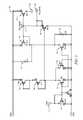
- FIG. 2illustrates a block diagram of the opto-isolator 20 in accordance with an illustrative embodiment.
- the opto-isolator 20has a transmitter IC 30 and a receiver IC 60 , which are typically implemented in a single IC package.
- the transmitter IC 30includes an electrical-to-optical converter (EOC) control circuit 35 having input interface logic (not shown) for receiving an electrical input signal to the opto-isolator 20 that is used to control the operations of an EOC 36 .
- the EOC 36is typically separate from the transmitter IC 30 and is usually made using a III-V process technology.
- the EOC 36is typically an LED
- the EOC 36will be referred to hereinafter as the “LED 36 ” and the EOC control circuit 35 will be referred to hereinafter as the “LED control circuit 35 ”.
- the LED 36is connected by wire bonds (not shown) to the transmitter IC 30 .
- a supply voltage VDD 1 and a ground reference GND 1are provided to the transmitter IC 30 .
- the transmitter IC 30includes a current source 37 for turning the LED 36 on and a shorting switch 38 that is controlled by the LED control circuit 35 to ensure that the LED 36 is turned off when it is supposed to be in the Off state.
- the capacitor 39represents the parasitic capacitance, Cparasitic 1 , between the bond wires going to the LED 36 and the ground reference node, GND 2 , of the receiver IC 60 .
- the transmitter IC 30includes a common mode pulse compensation (CMPC) circuit 50 that senses the current on a section of wire 41 and causes current to be added to the drive current of the LED 36 if the CMPC circuit 50 senses that a common mode pulse event is occurring.
- the wire 41has a parasitic capacitance, Cparasitic 2 , which is represented by capacitor 42 .
- the wire 41is connected to an input pad (not shown) of the CMPC circuit 50 and has an inherent parasitic capacitance to the nearby GND 2 of the receiver IC 60 . This sensed current corresponds to a common mode pulse.
- the CMPC circuit 50has a sensor 50 a and an auxiliary current source 50 b , which, as will be described below with reference to FIG. 3 , are combined into a single circuit.
- the auxiliary current source 50 bWhen the sensor 50 a senses a common mode pulse that has a negative slope and that is sufficiently great in magnitude to cause the opto-isolator 20 to operate improperly, the auxiliary current source 50 b outputs a positive pulse to the current source 37 .
- a common mode pulse that has a negative slope and that is sufficiently great in magnitude to cause the opto-isolator 20 to operate improperlywill be referred to herein as a “common mode pulse event”.
- the positive pulse that is output from the auxiliary current source 50 bcompensates for perturbations in the drive current caused by the sensed common mode pulse, thereby ensuring that the current source 37 will output a current that is appropriate for driving the LED 36 .
- the receiver IC 60 of the opto-isolator 20 shown in FIG. 2includes an optical-to-electrical converter (OEC) 61 , a TIA 62 , a comparator 63 and an output driver 64 .
- OECoptical-to-electrical converter
- the OEC 61is typically a photodiode, the OEC 61 will be referred to hereinafter as the “photodiode 61 ”.
- the optical output of the LED 36is coupled to the photodiode 61 on the receiver IC 60 .
- the photon input to the photodiode 61produces a corresponding photo current in the diode 61 .
- This currentis amplified in the TIA 62 and then the output is sent to the comparator 63 .
- the comparator 63compares the output from the TIA 62 to a reference voltage, VTH 1 , to determine whether the output corresponds to a logic 0 or logic 1 state and provides an output signal to the output driver 64 , which produces the output drive signal for the opto-isolator 20 at node 65 .
- the value of Cparasitic 2is typically in the range of 10 fF.
- the sensor 50 ais typically configured to detect a common mode pulse with a negative slope that is greater than or equal to about ⁇ 10 KV/ ⁇ sec.
- the auxiliary power source 50 boutputs a positive logic pulse to the current source 37 to increase the magnitude of the drive current that is being provided to the LED 36 .
- the CMPC circuit 50will now be described with reference to FIG. 3 .
- FIG. 3illustrates a schematic diagram of the CMPC circuit 50 in accordance with an embodiment.
- the CMPC circuit 50is made up of a plurality of n-type and p-type metal oxide semiconductor field effect transistors (MOSFETs) and a few diodes.
- a first input terminal 61 of the CMPC circuit 50receives a bias current, NBIAS.
- the bias current NBIAShas a positive polarity and is sufficiently large in amplitude to turn on an n-type MOSFET.
- the bias current NBIASis typically maintained in this state at all times during operation of the opto-isolator 20 .
- the bias current NBIASmay be provided to the CMPC circuit 50 by the LED control circuit 35 or by some other source external to the CMPC circuit 50 .
- a second input terminal 62 of the CMPC circuit 50is connected to an end of the section of wire 41 .
- the second input terminal 62will be referred to herein as the PAD_SENSE.
- the PAD_SENSE terminalis coupled by the parasitic capacitance Cparasitic 2 to the GND 2 of the receiver IC 60 .
- An output terminal 63 of the CMPC circuit 50is connected to the current source 37 .
- the combination of the n-type MOSFET 68 , also labeled MN 0 , and the n-type MOSFET MN 3 65form a 1-to-1 current minor that causes the bias current NBIAS being applied to the gate of MOSFET MN 0 68 to be replicated at the gate of MOSFET MN 3 65 .
- This bias current NBIASis typically a small current, e.g., 2.5 microamperes (uA), for the arrangement shown in FIG. 3 .
- the bias current NBIASalso turns on p-type MOSFETs MP 3 66 and MP 4 67 so that they are above threshold, but at a low current level.
- the combination of p-type MOSFETs MP 3 66 and MP 4 67forms a second current minor that causes the sensed current at the PAD_SENSE input terminal 62 to be applied to the gates p-type MOSFETs 66 and 67 .
- the slight bias current through p-type MOSFETs MP 3 66 and MP 4 67ensures that the PAD_SENSE node 71 will be sensitive to negatively-sloped common mode pulses that are coupled into parasitic capacitance Cparasitic 2 .
- the drain terminal of the p-type MOSFET MP 4 67is connected to the output terminal 63 .
- the p-type MOSFET MP 4 67has a width that is selected during the design phase so that the current passing through it and into the anode of the LED 36 via the current source 37 will have the value needed to compensate for the current being lost through Cparasitic 1 from the LED bond wire on the anode of the LED 36 .
- I_senseCparasitic 2 * ⁇ dV/dt.
- the ratio of the I_correction to I_senseis dependent on the ratio of the two parasitic capacitances, but not on the value of dV/dt, which is the slope of the sensed common mode pulse. This relationship provides the needed information from which the appropriate current gain ratio for the current minor made up of the p-type MOSFETs MP 3 66 and MP 4 67 current mirror. The result of the ratio situation is used to determine the width of MP 4 relative to MP 3 .
- the following equationrelates the widths of the p-type MOSFETs MP 3 66 and MP 4 67 to the parasitic capacitances Cparasitic 1 and Cparasitic 2 .
- W_MP 4 /W_MP 3Cparasitic 1 /Cparasitic 2 .
- CMPC circuit 50providing, via output terminal 63 , a correction current of the correct amplitude over a wide range of slope values, e.g., from about ⁇ 10 KV/ ⁇ sec up to about ⁇ 50 KV/ ⁇ sec.
- CMPC circuit 50provides, via output terminal 63 , a correction current of the correct amplitude over a wide range of slope values, e.g., from about ⁇ 10 KV/ ⁇ sec up to about ⁇ 50 KV/ ⁇ sec.
- the ratio of W_MP 4 to W_MP 3is 10 to 1.
- the width of p-type MOSFET MP 4 67is selected to be 10 times the width of p-type MOSFET MP 3 66 .
- the ratio of W_MP 4 to W_MP 3can be calculated using the above equation.
- the CMPC circuit 50becomes automatically adjustable to changes in the magnitude of the slope of a common mode pulse event. This feature extends the range of slopes for which the CMPC circuit 50 can react and provide compensation.
- the CMPC circuit 50is intentionally designed to compensate for negatively-sloped common mode pulse events, but not for positively-sloped common mode pulse events.
- a positively-sloped common mode pulse eventwill indeed result in an increase in the drive current of the LED 36 .
- the extra current added to the LED drive currentonly operates to turn the LED 36 on to an even greater extent, which will not cause errors out the output terminal 65 of the receiver IC 60 .
- LEDsare typically designed to handle short bursts of high drive current as well as lower current levels of relatively long duration. Therefore, compensation is not necessary for positively-sloped common mode pulse events in the CMPC circuit 50 .
- the CMPC circuit 50does provide protection for its components against positively-sloped common mode pulse events that are excessively large in magnitude, as will be described below in more detail. If the LED 36 is turned off during a positively-sloped common mode pulse event, the LED shorting switch 38 must handle the extra current to ensure that the LED 36 remains turned off. Prior to describing the manner in which the CMPC circuit 50 handles positively-sloped common mode pulse events, the manner in which the CMPC circuit 50 handles negatively-sloped common mode pulse events will be described.
- the CMPC circuit 50causes an additional amount of current to be added to the current source 37 via the connection between the output terminal 63 and the current source 37 , which is connected to the anode of the LED 36 .
- the additional currentwill be referred to hereinafter as the compensation current.
- the compensation current to be added to the current source 37is equal to AVDD divided by the resistance of the p-type MOSFET MP 4 67 .
- the compensation currentis generally equal to the current that is pulled away from the current source 37 as a result of the negatively-sloped common mode pulse event.
- the CMPC circuit 50includes additional MOSFETs MN 1 81 , MN 2 82 , MP 1 83 , MP 2 84 , and MP 5 85 , and two diodes D 0 86 and D 1 87 that are used to provide protection against excessively large positively-sloped common mode pulse events.
- the combination of the MOSFETs MN 1 81 , MN 2 82 , MP 1 83 , and MP 2 84generates a bias voltage for the gate of MOSFET 85 that is compensated for both temperature and process.
- the MOSFET MP 5 85will turn on, thereby causing the PAD_SENSE node 71 to be limited to slightly below the AVDD supply level, but high enough so that MP 3 66 and MP 4 67 are off. This causes the voltage at the PAD_SENSE node 71 to be clamped at a level that does not exceed the AVDD supply voltage level.
- the two diodes D 0 86 and D 1 87are additional elements for providing protection of circuit elements from excessive common mode transients.
- the CMPC circuit 50is not limited to the configuration shown in FIG. 3 . A number of different circuit configurations may be used to perform the compensation functions described above with reference to FIG. 3 .
- the CMPC circuit 50could be designed to compensate for both negatively-sloped and positively-sloped events, or to compensate for positively-sloped events rather than negatively-sloped events. In general, this could be accomplished by substituting the p-type MOSFETs with n-type MOSFETs or by adding additional n-type MOSFETs that duplicate the functions described above that are performed by the p-type MOSFETs.
- FIG. 4illustrates a flowchart that represents the method for performing common mode pulse compensation in an opto-isolator.
- a CMPC circuit of an opto-isolatorcommon mode pulses are sensed to determine whether a common mode pulse event is occurring, as indicated by block 101 .
- the CMPC circuitis capable of reacting extremely quickly so that common mode pulse events are compensated for as the events are occurring. If a common mode pulse event is occurring, then the CMPC circuit generates a compensation current to be added to the LED drive current, as indicated by block 102 .
- the compensation currentis output from the CMPC circuit, as indicated by block 103 , and added to the LED drive current to obtain a new LED drive current, as indicated by block 104 .
- the new LED drive currentis used in the opto-isolator to drive the LED, as indicated by block 105 .
- FIGS. 3 and 4are merely examples of embodiments that are suitable for performing the functions needed to compensate the LED drive current.
- a variety of circuitscan be designed to perform these tasks, and all such variations or modifications to the embodiments described herein are within the scope of the invention.
- the opto-isolatorhas been described as having a transmitter and a receiver IC that are contained in the same IC package, these may be implemented in two or more ICs, and may even be implemented using discrete components.
- the EOC of the transmitter ICis described herein as being an LED, the EOC may be any type of light source, including laser diodes and other devices.
- the OEC of the receiver circuitis described herein as being a photodiode, the OEC may be any type of device that converts optical energy into electrical energy.
- Other variations and modificationsmay be made to the embodiments described herein, as will be understood by those skilled in the art, and such modifications and variations are within the scope of the invention.
Landscapes
- Physics & Mathematics (AREA)
- Electromagnetism (AREA)
- Engineering & Computer Science (AREA)
- Computer Networks & Wireless Communication (AREA)
- Signal Processing (AREA)
- Photo Coupler, Interrupter, Optical-To-Optical Conversion Devices (AREA)
- Electronic Switches (AREA)
- Optical Communication System (AREA)
- Amplifiers (AREA)
Abstract
Description
I_error=Cparasitic*−dV/dT,
where I_error represents the portion of the drive current pulled away from the LED6 by the parasitic capacitor9, Cparasitic represents the parasitic capacitance, and dV/dT represents the slope of the common mode pulse. The negative sign means the GND2 potential decreases with respect to GND1. Using this equation, it can be determined that for a common mode pulse having a slope of −10 KV/μsec, the current I_error through a typical Cparasitic value of 50 femptofarads (fF) is 0.5 milliamperes (mA). This current level is relatively high, which means that a significant portion of the drive current for the LED6 has been pulled through the parasitic capacitance and thereby diverted from the LED6. This reduces the optical output of the LED6 and may cause the corresponding signal output from the
I_correction=Cparasitic1*−dV/dt.
W_MP4/W_MP3=Cparasitic1/Cparasitic2.
Claims (14)
Priority Applications (3)
| Application Number | Priority Date | Filing Date | Title |
|---|---|---|---|
| US12/719,036US8116055B2 (en) | 2007-06-21 | 2010-03-08 | Methods and apparatuses for performing common mode pulse compensation in an opto-isolator |
| DE102011005213ADE102011005213A1 (en) | 2010-03-08 | 2011-03-07 | Method and apparatus for performing common mode pulse compensation in an opto-isolator |
| JP2011050156AJP5666351B2 (en) | 2010-03-08 | 2011-03-08 | Method and apparatus for performing common mode pulse compensation in an optoisolator |
Applications Claiming Priority (2)
| Application Number | Priority Date | Filing Date | Title |
|---|---|---|---|
| US11/766,333US7808759B2 (en) | 2007-06-21 | 2007-06-21 | Methods and apparatuses for performing common mode pulse compensation in an opto-isolator |
| US12/719,036US8116055B2 (en) | 2007-06-21 | 2010-03-08 | Methods and apparatuses for performing common mode pulse compensation in an opto-isolator |
Related Parent Applications (1)
| Application Number | Title | Priority Date | Filing Date |
|---|---|---|---|
| US11/766,333Continuation-In-PartUS7808759B2 (en) | 2007-06-21 | 2007-06-21 | Methods and apparatuses for performing common mode pulse compensation in an opto-isolator |
Publications (2)
| Publication Number | Publication Date |
|---|---|
| US20100155627A1 US20100155627A1 (en) | 2010-06-24 |
| US8116055B2true US8116055B2 (en) | 2012-02-14 |
Family
ID=44793795
Family Applications (1)
| Application Number | Title | Priority Date | Filing Date |
|---|---|---|---|
| US12/719,036Expired - Fee RelatedUS8116055B2 (en) | 2007-06-21 | 2010-03-08 | Methods and apparatuses for performing common mode pulse compensation in an opto-isolator |
Country Status (3)
| Country | Link |
|---|---|
| US (1) | US8116055B2 (en) |
| JP (1) | JP5666351B2 (en) |
| DE (1) | DE102011005213A1 (en) |
Cited By (7)
| Publication number | Priority date | Publication date | Assignee | Title |
|---|---|---|---|---|
| US20100266292A1 (en)* | 2009-04-15 | 2010-10-21 | Nec Electronics Corporation | Light receiving circuit and photocoupler isolation circuit |
| US20120298890A1 (en)* | 2010-01-19 | 2012-11-29 | Johnson Controls Technology Company | Optocoupler circuit for gate driver |
| US9660848B2 (en) | 2014-09-15 | 2017-05-23 | Analog Devices Global | Methods and structures to generate on/off keyed carrier signals for signal isolators |
| US9998301B2 (en) | 2014-11-03 | 2018-06-12 | Analog Devices, Inc. | Signal isolator system with protection for common mode transients |
| US10069574B2 (en) | 2015-10-01 | 2018-09-04 | Avago Technologies General Ip (Singapore) Pte. Ltd. | Optocoupler with indication of light source power supply failure |
| US10270630B2 (en) | 2014-09-15 | 2019-04-23 | Analog Devices, Inc. | Demodulation of on-off-key modulated signals in signal isolator systems |
| US10536309B2 (en) | 2014-09-15 | 2020-01-14 | Analog Devices, Inc. | Demodulation of on-off-key modulated signals in signal isolator systems |
Families Citing this family (6)
| Publication number | Priority date | Publication date | Assignee | Title |
|---|---|---|---|---|
| US8983304B2 (en)* | 2012-10-25 | 2015-03-17 | Avago Technologies General Ip (Singapore) Pte. Ltd. | Opto-isolator with compensation circuit |
| US10075246B2 (en) | 2013-09-26 | 2018-09-11 | Micro Motion, Inc. | Optical isolator mounted in printed circuit board recess |
| US9175993B2 (en)* | 2013-09-26 | 2015-11-03 | Rosemount Inc. | Industrial process field device with low power optical isolator |
| US9228869B2 (en) | 2013-09-26 | 2016-01-05 | Rosemount Inc. | Industrial process variable transmitter with isolated power scavenging intrinsically safe pulse output circuitry |
| US10044447B2 (en)* | 2016-04-04 | 2018-08-07 | Biosense Webster (Israel) Ltd. | Linear isolation amplifier with output DC voltage cancellation |
| JP2020113602A (en)* | 2019-01-09 | 2020-07-27 | 株式会社東芝 | Semiconductor device |
Citations (16)
| Publication number | Priority date | Publication date | Assignee | Title |
|---|---|---|---|---|
| US4568838A (en) | 1981-05-29 | 1986-02-04 | Hitachi, Ltd. | Control circuit for a semiconductor element with a control electrode |
| US5043587A (en) | 1989-01-17 | 1991-08-27 | Fuji Electric Co., Ltd. | Photocoupler circuit having DC power source in series with detection and switching means |
| US5089948A (en) | 1990-06-29 | 1992-02-18 | Digital Equipment Corporation | High speed optoisolator switching apparatus |
| US5465298A (en) | 1994-04-14 | 1995-11-07 | Cermetek Microelectronics | Solid state isolation device using opto-isolators |
| US20030048008A1 (en) | 2001-09-12 | 2003-03-13 | Thierry Castagnet | Current-limiting logic interface circuit |
| US6586890B2 (en) | 2001-12-05 | 2003-07-01 | Koninklijke Philips Electronics N.V. | LED driver circuit with PWM output |
| US20050225976A1 (en) | 2004-04-08 | 2005-10-13 | Integrated Illumination Systems, Inc. | Marine LED lighting network and driver |
| US20070115248A1 (en) | 2005-11-18 | 2007-05-24 | Roberts John K | Solid state lighting panels with variable voltage boost current sources |
| US7253997B2 (en) | 1999-09-24 | 2007-08-07 | Power Integrations, Inc. | Method and apparatus providing a multi-function terminal for a power supply controller |
| US20080062606A1 (en) | 2006-03-15 | 2008-03-13 | Brown Kenneth J | Surge protection device for coaxial cable with diagnostic capabilities |
| US20080169834A1 (en) | 2003-04-30 | 2008-07-17 | Baoxing Chen | Signal isolators using micro-transformers |
| US7420335B2 (en) | 2004-06-30 | 2008-09-02 | Tir Technology Lp | Switched constant current driving and control circuit |
| US20080292325A1 (en) | 2007-05-21 | 2008-11-27 | Lei Chen | High immunity clock regeneration over optically isolated channel |
| US20080308817A1 (en) | 2007-06-12 | 2008-12-18 | Youfa Wang | Galvanic Isolator Having Improved High Voltage Common Mode Transient Immunity |
| US20080315925A1 (en) | 2007-06-25 | 2008-12-25 | Alfano Donald E | Isolator circuit including a voltage regulator |
| US7482666B2 (en) | 2006-01-12 | 2009-01-27 | Silicon Laboratories Inc. | Apparatus and method for optical isolation |
Family Cites Families (1)
| Publication number | Priority date | Publication date | Assignee | Title |
|---|---|---|---|---|
| US8031A (en)* | 1851-04-08 | Gkraih separator and ban |
- 2010
- 2010-03-08USUS12/719,036patent/US8116055B2/ennot_activeExpired - Fee Related
- 2011
- 2011-03-07DEDE102011005213Apatent/DE102011005213A1/ennot_activeWithdrawn
- 2011-03-08JPJP2011050156Apatent/JP5666351B2/enactiveActive
Patent Citations (16)
| Publication number | Priority date | Publication date | Assignee | Title |
|---|---|---|---|---|
| US4568838A (en) | 1981-05-29 | 1986-02-04 | Hitachi, Ltd. | Control circuit for a semiconductor element with a control electrode |
| US5043587A (en) | 1989-01-17 | 1991-08-27 | Fuji Electric Co., Ltd. | Photocoupler circuit having DC power source in series with detection and switching means |
| US5089948A (en) | 1990-06-29 | 1992-02-18 | Digital Equipment Corporation | High speed optoisolator switching apparatus |
| US5465298A (en) | 1994-04-14 | 1995-11-07 | Cermetek Microelectronics | Solid state isolation device using opto-isolators |
| US7253997B2 (en) | 1999-09-24 | 2007-08-07 | Power Integrations, Inc. | Method and apparatus providing a multi-function terminal for a power supply controller |
| US20030048008A1 (en) | 2001-09-12 | 2003-03-13 | Thierry Castagnet | Current-limiting logic interface circuit |
| US6586890B2 (en) | 2001-12-05 | 2003-07-01 | Koninklijke Philips Electronics N.V. | LED driver circuit with PWM output |
| US20080169834A1 (en) | 2003-04-30 | 2008-07-17 | Baoxing Chen | Signal isolators using micro-transformers |
| US20050225976A1 (en) | 2004-04-08 | 2005-10-13 | Integrated Illumination Systems, Inc. | Marine LED lighting network and driver |
| US7420335B2 (en) | 2004-06-30 | 2008-09-02 | Tir Technology Lp | Switched constant current driving and control circuit |
| US20070115248A1 (en) | 2005-11-18 | 2007-05-24 | Roberts John K | Solid state lighting panels with variable voltage boost current sources |
| US7482666B2 (en) | 2006-01-12 | 2009-01-27 | Silicon Laboratories Inc. | Apparatus and method for optical isolation |
| US20080062606A1 (en) | 2006-03-15 | 2008-03-13 | Brown Kenneth J | Surge protection device for coaxial cable with diagnostic capabilities |
| US20080292325A1 (en) | 2007-05-21 | 2008-11-27 | Lei Chen | High immunity clock regeneration over optically isolated channel |
| US20080308817A1 (en) | 2007-06-12 | 2008-12-18 | Youfa Wang | Galvanic Isolator Having Improved High Voltage Common Mode Transient Immunity |
| US20080315925A1 (en) | 2007-06-25 | 2008-12-25 | Alfano Donald E | Isolator circuit including a voltage regulator |
Non-Patent Citations (2)
| Title |
|---|
| Hewlett-Packard, "Insulation and Regulation of Optically Coupled Isolation Devices"; http://www.secomtel.com/ UpFilesPDF/PDF/Agilent/PDF-DOCS/ISONCONT/01-OPTO/optocouplerdg.pdf; Nov. 12, 1999; Designer's Guide, 70 pages. |
| Hewlett-Packard, , "Insulation and Regulation of Optically Coupled Isolation Devices", http://www.secomtel.com/UpFilesPDF/PDF/Agilent/PDF-DOCS/ISONCONT/01-OPTO/optocouplerdg.pdf Nov. 12, 1999. |
Cited By (9)
| Publication number | Priority date | Publication date | Assignee | Title |
|---|---|---|---|---|
| US20100266292A1 (en)* | 2009-04-15 | 2010-10-21 | Nec Electronics Corporation | Light receiving circuit and photocoupler isolation circuit |
| US8280262B2 (en)* | 2009-04-15 | 2012-10-02 | Renesas Electronics Corporation | Light receiving circuit and photocoupler isolation circuit |
| US20120298890A1 (en)* | 2010-01-19 | 2012-11-29 | Johnson Controls Technology Company | Optocoupler circuit for gate driver |
| US8624213B2 (en)* | 2010-01-19 | 2014-01-07 | Johnson Controls Technology Company | Optocoupler circuit for gate driver |
| US9660848B2 (en) | 2014-09-15 | 2017-05-23 | Analog Devices Global | Methods and structures to generate on/off keyed carrier signals for signal isolators |
| US10270630B2 (en) | 2014-09-15 | 2019-04-23 | Analog Devices, Inc. | Demodulation of on-off-key modulated signals in signal isolator systems |
| US10536309B2 (en) | 2014-09-15 | 2020-01-14 | Analog Devices, Inc. | Demodulation of on-off-key modulated signals in signal isolator systems |
| US9998301B2 (en) | 2014-11-03 | 2018-06-12 | Analog Devices, Inc. | Signal isolator system with protection for common mode transients |
| US10069574B2 (en) | 2015-10-01 | 2018-09-04 | Avago Technologies General Ip (Singapore) Pte. Ltd. | Optocoupler with indication of light source power supply failure |
Also Published As
| Publication number | Publication date |
|---|---|
| DE102011005213A1 (en) | 2011-12-15 |
| JP5666351B2 (en) | 2015-02-12 |
| JP2011187960A (en) | 2011-09-22 |
| US20100155627A1 (en) | 2010-06-24 |
Similar Documents
| Publication | Publication Date | Title |
|---|---|---|
| US8116055B2 (en) | Methods and apparatuses for performing common mode pulse compensation in an opto-isolator | |
| US6788152B2 (en) | Amplification circuit and optical communication apparatus provided with the amplification circuit | |
| US20180275280A1 (en) | High dynamic range analog front-end receiver for long range lidar | |
| US6643472B1 (en) | APD bias circuit | |
| US8373405B2 (en) | Power supply voltage detection circuit | |
| CN101630044B (en) | Optical receiver | |
| CN112803901B (en) | A power amplifier based on adaptive overcurrent protection | |
| TWI386104B (en) | Protection circuit and method | |
| US20070268642A1 (en) | Integrated programmable over-current protection circuit for optical transmitters | |
| US20070139839A1 (en) | Overcurrent detection circuit and switching circuit | |
| US20090273874A1 (en) | Power switch circuit exhibiting over current and short circuit protection and method for limiting the output current thereof | |
| KR20140042466A (en) | Clamping circuit, semiconductor having the same and clamping method thereof | |
| US7542684B2 (en) | Light emitting diode driving device and optical transmission device including the same | |
| CN109448621B (en) | Drive circuit and display device | |
| JP6271372B2 (en) | Optical receiving circuit and optical coupling device | |
| US8073030B2 (en) | Shunt driver circuit for semiconductor laser diode | |
| US20080087851A1 (en) | Current Transfer Ratio Temperature Coefficient Compensation Method And Apparatus | |
| US8129671B2 (en) | Power supply dependent optical receiver and amplifier and photocoupler using the same | |
| US20080118252A1 (en) | Optical coupler with reduced pulse width distortion | |
| US5386109A (en) | Pre-amplifier for optical receiving and optical receiver using the same | |
| JP5003586B2 (en) | Semiconductor laser drive circuit | |
| US7808759B2 (en) | Methods and apparatuses for performing common mode pulse compensation in an opto-isolator | |
| JP2009207144A (en) | Circuit and method for signal voltage transmission within driver circuit of power semiconductor switch | |
| US7936216B2 (en) | True current limiting | |
| JP3402674B2 (en) | Optical receiving preamplifier and optical receiving apparatus |
Legal Events
| Date | Code | Title | Description |
|---|---|---|---|
| AS | Assignment | Owner name:AVAGO TECHNOLOGIES ECBU IP (SINGAPORE) PTE. LTD.,S Free format text:ASSIGNMENT OF ASSIGNORS INTEREST;ASSIGNORS:BAUMGARTNER, RICHARD A.;CHANG, KWEE CHONG;SIGNING DATES FROM 20100305 TO 20100308;REEL/FRAME:024057/0836 Owner name:AVAGO TECHNOLOGIES ECBU IP (SINGAPORE) PTE. LTD., Free format text:ASSIGNMENT OF ASSIGNORS INTEREST;ASSIGNORS:BAUMGARTNER, RICHARD A.;CHANG, KWEE CHONG;SIGNING DATES FROM 20100305 TO 20100308;REEL/FRAME:024057/0836 | |
| ZAAA | Notice of allowance and fees due | Free format text:ORIGINAL CODE: NOA | |
| ZAAB | Notice of allowance mailed | Free format text:ORIGINAL CODE: MN/=. | |
| STCF | Information on status: patent grant | Free format text:PATENTED CASE | |
| AS | Assignment | Owner name:AVAGO TECHNOLOGIES GENERAL IP (SINGAPORE) PTE. LTD Free format text:MERGER;ASSIGNOR:AVAGO TECHNOLOGIES ECBU IP (SINGAPORE) PTE. LTD.;REEL/FRAME:030369/0528 Effective date:20121030 | |
| AS | Assignment | Owner name:DEUTSCHE BANK AG NEW YORK BRANCH, AS COLLATERAL AGENT, NEW YORK Free format text:PATENT SECURITY AGREEMENT;ASSIGNOR:AVAGO TECHNOLOGIES GENERAL IP (SINGAPORE) PTE. LTD.;REEL/FRAME:032851/0001 Effective date:20140506 Owner name:DEUTSCHE BANK AG NEW YORK BRANCH, AS COLLATERAL AG Free format text:PATENT SECURITY AGREEMENT;ASSIGNOR:AVAGO TECHNOLOGIES GENERAL IP (SINGAPORE) PTE. LTD.;REEL/FRAME:032851/0001 Effective date:20140506 | |
| FPAY | Fee payment | Year of fee payment:4 | |
| AS | Assignment | Owner name:AVAGO TECHNOLOGIES GENERAL IP (SINGAPORE) PTE. LTD., SINGAPORE Free format text:TERMINATION AND RELEASE OF SECURITY INTEREST IN PATENT RIGHTS (RELEASES RF 032851-0001);ASSIGNOR:DEUTSCHE BANK AG NEW YORK BRANCH, AS COLLATERAL AGENT;REEL/FRAME:037689/0001 Effective date:20160201 Owner name:AVAGO TECHNOLOGIES GENERAL IP (SINGAPORE) PTE. LTD Free format text:TERMINATION AND RELEASE OF SECURITY INTEREST IN PATENT RIGHTS (RELEASES RF 032851-0001);ASSIGNOR:DEUTSCHE BANK AG NEW YORK BRANCH, AS COLLATERAL AGENT;REEL/FRAME:037689/0001 Effective date:20160201 | |
| AS | Assignment | Owner name:BANK OF AMERICA, N.A., AS COLLATERAL AGENT, NORTH CAROLINA Free format text:PATENT SECURITY AGREEMENT;ASSIGNOR:AVAGO TECHNOLOGIES GENERAL IP (SINGAPORE) PTE. LTD.;REEL/FRAME:037808/0001 Effective date:20160201 Owner name:BANK OF AMERICA, N.A., AS COLLATERAL AGENT, NORTH Free format text:PATENT SECURITY AGREEMENT;ASSIGNOR:AVAGO TECHNOLOGIES GENERAL IP (SINGAPORE) PTE. LTD.;REEL/FRAME:037808/0001 Effective date:20160201 | |
| AS | Assignment | Owner name:AVAGO TECHNOLOGIES GENERAL IP (SINGAPORE) PTE. LTD., SINGAPORE Free format text:TERMINATION AND RELEASE OF SECURITY INTEREST IN PATENTS;ASSIGNOR:BANK OF AMERICA, N.A., AS COLLATERAL AGENT;REEL/FRAME:041710/0001 Effective date:20170119 Owner name:AVAGO TECHNOLOGIES GENERAL IP (SINGAPORE) PTE. LTD Free format text:TERMINATION AND RELEASE OF SECURITY INTEREST IN PATENTS;ASSIGNOR:BANK OF AMERICA, N.A., AS COLLATERAL AGENT;REEL/FRAME:041710/0001 Effective date:20170119 | |
| AS | Assignment | Owner name:AVAGO TECHNOLOGIES INTERNATIONAL SALES PTE. LIMITE Free format text:MERGER;ASSIGNOR:AVAGO TECHNOLOGIES GENERAL IP (SINGAPORE) PTE. LTD.;REEL/FRAME:047230/0133 Effective date:20180509 | |
| AS | Assignment | Owner name:AVAGO TECHNOLOGIES INTERNATIONAL SALES PTE. LIMITE Free format text:CORRECTIVE ASSIGNMENT TO CORRECT THE EFFECTIVE DATE OF MERGER TO 09/05/2018 PREVIOUSLY RECORDED AT REEL: 047230 FRAME: 0133. ASSIGNOR(S) HEREBY CONFIRMS THE MERGER;ASSIGNOR:AVAGO TECHNOLOGIES GENERAL IP (SINGAPORE) PTE. LTD.;REEL/FRAME:047630/0456 Effective date:20180905 | |
| MAFP | Maintenance fee payment | Free format text:PAYMENT OF MAINTENANCE FEE, 8TH YEAR, LARGE ENTITY (ORIGINAL EVENT CODE: M1552); ENTITY STATUS OF PATENT OWNER: LARGE ENTITY Year of fee payment:8 | |
| FEPP | Fee payment procedure | Free format text:MAINTENANCE FEE REMINDER MAILED (ORIGINAL EVENT CODE: REM.); ENTITY STATUS OF PATENT OWNER: LARGE ENTITY | |
| LAPS | Lapse for failure to pay maintenance fees | Free format text:PATENT EXPIRED FOR FAILURE TO PAY MAINTENANCE FEES (ORIGINAL EVENT CODE: EXP.); ENTITY STATUS OF PATENT OWNER: LARGE ENTITY | |
| STCH | Information on status: patent discontinuation | Free format text:PATENT EXPIRED DUE TO NONPAYMENT OF MAINTENANCE FEES UNDER 37 CFR 1.362 | |
| FP | Lapsed due to failure to pay maintenance fee | Effective date:20240214 |