US8116043B2 - Method and system for providing a magnetic transducer having an improved read sensor synthetic antiferromagnet - Google Patents
Method and system for providing a magnetic transducer having an improved read sensor synthetic antiferromagnetDownload PDFInfo
- Publication number
- US8116043B2 US8116043B2US12/634,589US63458909AUS8116043B2US 8116043 B2US8116043 B2US 8116043B2US 63458909 AUS63458909 AUS 63458909AUS 8116043 B2US8116043 B2US 8116043B2
- Authority
- US
- United States
- Prior art keywords
- sublayer
- layer
- thickness
- angstroms
- exchange energy
- Prior art date
- Legal status (The legal status is an assumption and is not a legal conclusion. Google has not performed a legal analysis and makes no representation as to the accuracy of the status listed.)
- Expired - Fee Related, expires
Links
- 230000005291magnetic effectEffects0.000titleclaimsabstractdescription81
- 238000000034methodMethods0.000titleclaimsabstractdescription25
- 230000005290antiferromagnetic effectEffects0.000claimsabstractdescription12
- 125000006850spacer groupChemical group0.000claimsabstractdescription11
- 230000000903blocking effectEffects0.000claimsabstractdescription6
- 229910020913Co1-xFexInorganic materials0.000claimsdescription13
- 230000004888barrier functionEffects0.000claimsdescription7
- 230000005641tunnelingEffects0.000claimsdescription6
- 238000000059patterningMethods0.000claims1
- 239000010410layerSubstances0.000description152
- 230000005415magnetizationEffects0.000description12
- 239000000463materialSubstances0.000description12
- 239000006185dispersionSubstances0.000description9
- 230000005294ferromagnetic effectEffects0.000description7
- 239000000758substrateSubstances0.000description4
- 230000003993interactionEffects0.000description3
- 230000002411adverseEffects0.000description2
- 239000000470constituentSubstances0.000description2
- 238000004519manufacturing processMethods0.000description2
- 239000000203mixtureSubstances0.000description2
- 229910001030Iron–nickel alloyInorganic materials0.000description1
- 230000015572biosynthetic processEffects0.000description1
- 230000008859changeEffects0.000description1
- 238000010586diagramMethods0.000description1
- 230000006872improvementEffects0.000description1
- 238000003801millingMethods0.000description1
- 238000007747platingMethods0.000description1
- 230000004044responseEffects0.000description1
- 239000002356single layerSubstances0.000description1
Images


Classifications
- G—PHYSICS
- G01—MEASURING; TESTING
- G01R—MEASURING ELECTRIC VARIABLES; MEASURING MAGNETIC VARIABLES
- G01R33/00—Arrangements or instruments for measuring magnetic variables
- G01R33/02—Measuring direction or magnitude of magnetic fields or magnetic flux
- G01R33/06—Measuring direction or magnitude of magnetic fields or magnetic flux using galvano-magnetic devices
- G01R33/09—Magnetoresistive devices
- G01R33/098—Magnetoresistive devices comprising tunnel junctions, e.g. tunnel magnetoresistance sensors
- B—PERFORMING OPERATIONS; TRANSPORTING
- B82—NANOTECHNOLOGY
- B82Y—SPECIFIC USES OR APPLICATIONS OF NANOSTRUCTURES; MEASUREMENT OR ANALYSIS OF NANOSTRUCTURES; MANUFACTURE OR TREATMENT OF NANOSTRUCTURES
- B82Y10/00—Nanotechnology for information processing, storage or transmission, e.g. quantum computing or single electron logic
- B—PERFORMING OPERATIONS; TRANSPORTING
- B82—NANOTECHNOLOGY
- B82Y—SPECIFIC USES OR APPLICATIONS OF NANOSTRUCTURES; MEASUREMENT OR ANALYSIS OF NANOSTRUCTURES; MANUFACTURE OR TREATMENT OF NANOSTRUCTURES
- B82Y25/00—Nanomagnetism, e.g. magnetoimpedance, anisotropic magnetoresistance, giant magnetoresistance or tunneling magnetoresistance
- G—PHYSICS
- G11—INFORMATION STORAGE
- G11B—INFORMATION STORAGE BASED ON RELATIVE MOVEMENT BETWEEN RECORD CARRIER AND TRANSDUCER
- G11B5/00—Recording by magnetisation or demagnetisation of a record carrier; Reproducing by magnetic means; Record carriers therefor
- G11B5/127—Structure or manufacture of heads, e.g. inductive
- G11B5/33—Structure or manufacture of flux-sensitive heads, i.e. for reproduction only; Combination of such heads with means for recording or erasing only
- G11B5/39—Structure or manufacture of flux-sensitive heads, i.e. for reproduction only; Combination of such heads with means for recording or erasing only using magneto-resistive devices or effects
- G11B5/3903—Structure or manufacture of flux-sensitive heads, i.e. for reproduction only; Combination of such heads with means for recording or erasing only using magneto-resistive devices or effects using magnetic thin film layers or their effects, the films being part of integrated structures
- G11B5/3906—Details related to the use of magnetic thin film layers or to their effects
- G11B5/3909—Arrangements using a magnetic tunnel junction
- G—PHYSICS
- G11—INFORMATION STORAGE
- G11B—INFORMATION STORAGE BASED ON RELATIVE MOVEMENT BETWEEN RECORD CARRIER AND TRANSDUCER
- G11B5/00—Recording by magnetisation or demagnetisation of a record carrier; Reproducing by magnetic means; Record carriers therefor
- G11B5/127—Structure or manufacture of heads, e.g. inductive
- G11B5/33—Structure or manufacture of flux-sensitive heads, i.e. for reproduction only; Combination of such heads with means for recording or erasing only
- G11B5/39—Structure or manufacture of flux-sensitive heads, i.e. for reproduction only; Combination of such heads with means for recording or erasing only using magneto-resistive devices or effects
- G11B2005/3996—Structure or manufacture of flux-sensitive heads, i.e. for reproduction only; Combination of such heads with means for recording or erasing only using magneto-resistive devices or effects large or giant magnetoresistive effects [GMR], e.g. as generated in spin-valve [SV] devices
- Y—GENERAL TAGGING OF NEW TECHNOLOGICAL DEVELOPMENTS; GENERAL TAGGING OF CROSS-SECTIONAL TECHNOLOGIES SPANNING OVER SEVERAL SECTIONS OF THE IPC; TECHNICAL SUBJECTS COVERED BY FORMER USPC CROSS-REFERENCE ART COLLECTIONS [XRACs] AND DIGESTS
- Y10—TECHNICAL SUBJECTS COVERED BY FORMER USPC
- Y10T—TECHNICAL SUBJECTS COVERED BY FORMER US CLASSIFICATION
- Y10T29/00—Metal working
- Y10T29/49—Method of mechanical manufacture
- Y10T29/49002—Electrical device making
- Y10T29/4902—Electromagnet, transformer or inductor
- Y10T29/49021—Magnetic recording reproducing transducer [e.g., tape head, core, etc.]
- Y10T29/49032—Fabricating head structure or component thereof
- Y—GENERAL TAGGING OF NEW TECHNOLOGICAL DEVELOPMENTS; GENERAL TAGGING OF CROSS-SECTIONAL TECHNOLOGIES SPANNING OVER SEVERAL SECTIONS OF THE IPC; TECHNICAL SUBJECTS COVERED BY FORMER USPC CROSS-REFERENCE ART COLLECTIONS [XRACs] AND DIGESTS
- Y10—TECHNICAL SUBJECTS COVERED BY FORMER USPC
- Y10T—TECHNICAL SUBJECTS COVERED BY FORMER US CLASSIFICATION
- Y10T428/00—Stock material or miscellaneous articles
- Y10T428/11—Magnetic recording head
- Y10T428/1107—Magnetoresistive
- Y10T428/1121—Multilayer
Definitions
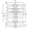
- FIG. 1depicts a portion of a conventional magnetic transducer 10 , such as a conventional read transducer or other device.
- the conventional transducer 10resides on a conventional substrate 11 , such as an AlTiC substrate.
- the conventional transducer 10includes a conventional bottom shield 12 , conventional sensor 20 , and conventional top shield 40 .
- the transducer 10also typically includes seed layer(s) (not shown) between the conventional AFM layer 22 and the conventional shield 12 .
- the conventional shields 12 and 40typically include NiFe and are formed by plating.
- the sensor 20is shown in a current-perpendicular to plane (CPP) configuration. In a CPP configuration, read current is driven generally perpendicular to the plane of the layers of the device, along the z-axis shown.
- CPPcurrent-perpendicular to plane
- the conventional sensor 20includes a conventional antiferromagnetic (AFM) layer 22 , a conventional synthetic antiferromagnet (SAF) 24 , a conventional barrier layer 32 , a conventional free layer 34 , and may include a conventional capping layer 36 .
- the conventional free layer 34has a magnetization that is substantially free to change direction in response to an applied magnetic field, for example from a bit being read.
- the conventional barrier layer 32may allow conduction through the sensor 20 via tunneling.
- the sensor 20is thus a tunneling magnetoresistive (TMR) sensor. Note that if a conductive spacer layer is used instead of the barrier layer 32 , then the sensor 20 is a spin valve.
- the conventional SAF layer 24typically includes two ferromagnetic layers 26 and 30 separated by a nonmagnetic spacer layer 28 .
- the ferromagnetic layersare generally antiferromagnetically coupled.
- the magnetization(s) of the conventional SAF layer 24are pinned by the conventional AFM layer 22 .
- the first ferromagnetic layer 26typically termed the pinned layer, has its magnetization pinned by the conventional AFM layer 22 , for example via exchange interaction.
- the remaining ferromagnetic layer, or reference layer 30has its magnetization pinned because it is strongly magnetically coupled with the pinned layer 26 .
- the conventional pinned layer 26is typically a single layer, for example composed of Co 90 Fe 10 .
- Other conventional pinned layers 26may be composed of Co 75 Fe 25 .
- BLPbaseline popping
- BLNbaseline line noise
- BLPrefers to time domain random noise spikes above the noise baseline.
- BLNrefers to high overall noise baseline.
- Both BLP and BLNare of large frequency bandwidth, generally ranging from KHz to GHz.
- BLP and BLNmay also be significant failure modes in hard disk drive applications of the conventional sensor 20 . Because they may be failure modes, BLN and BLP may also adversely affect reliability of the conventional sensor 20 .
- use of the conventional transducer 10may have drawbacks.
- a method and system for providing a magnetic structure in magnetic transducerincludes providing a pinning layer, a synthetic antiferromagnetic (SAF) adjacent to the pinning layer, a nonmagnetic layer, and a sensor layer.
- the SAFresides between the nonmagnetic layer and the pinning layer.
- the nonmagnetic layeris between the SAF and the sensor layer.
- the SAFincludes a pinned layer, a reference layer, and a nonmagnetic spacer layer between the pinned layer and the reference layer.
- the pinned layeris magnetically coupled with the reference layer and includes a plurality of sublayers.
- a first sublayer of the plurality of sublayershas a first blocking temperature distribution (T BD ) and a first exchange energy.
- T BDblocking temperature distribution
- a second sublayer of the plurality of sublayershas a second T BD and a second exchange energy.
- the first sublayeris between the pinning layer and the second sublayer.
- the first T BDis greater than the second T BD , while the first exchange energy is less than the second exchange energy.
- FIG. 1is a diagram of a portion of a conventional transducer including a conventional sensor.
- FIG. 2depicts an exemplary embodiment of a head having a transducer including an exemplary embodiment of a magnetic structure.
- FIG. 3depicts an exemplary embodiment of a portion of transducer including an exemplary embodiment of a magnetic structure.
- FIG. 4depicts another exemplary embodiment of a portion of transducer including an exemplary embodiment of a magnetic structure.
- FIG. 5depicts another exemplary embodiment of a portion of transducer including an exemplary embodiment of a magnetic structure.
- FIG. 6depicts an exemplary embodiment of a method of forming a portion of transducer including an exemplary embodiment of a magnetic structure.
- FIG. 2depicts a magnetic head 100 .
- the magnetic headincludes a magnetic read transducer 110 and write transducer 140 .
- FIG. 3depicts an exemplary embodiment of a magnetic structure 130 that may be used as the read sensor of the magnetic head 100 .
- the magnetic structure 130may be used for other purposes.
- the magnetic structure 130is shown in a CPP configuration, and thus is attached to the shields 112 and 122 .
- a gapmay exist between the magnetic structure 130 and the shields 112 and/or 122 .
- the head 100might include only the read transducer 110 .
- the head 100may reside on a slider (not shown) of a disk drive (not shown).
- the head 100is also described in the context of particular layers. However, in some embodiments, such layers may include sub-layer(s). For clarity, FIGS. 2-3 are not drawn to scale.
- the write transducer 140includes a first pole 142 , auxiliary pole 146 , main pole 148 , write gap 150 , coils 144 and 152 , and return shield 154 .
- the write transducer 140other and/or different components.
- one or more portions of the write transducer 140might be omitted in various embodiments.
- the read transducer 110includes shields 112 and 122 and read sensor/magnetic structure 130 .
- the magnetic structure 130might be used for other purposes in another transducer.
- the magnetic structure 130includes a pinning layer 160 , a SAF 170 , a nonmagnetic layer 190 , and a free layer 192 .
- other componentsmay be included as part of the magnetic structure 130 .
- the magnetic structure 130might also include seed layer(s) and/or capping layers.
- the free layer 192includes one or more ferromagnetic layers (not separately shown in FIG. 3 ). At least some of these ferromagnetic layers may be spaced by nonmagnetic layers. In the embodiment shown in FIG. 3 , the free layer 192 is a sensor layer for the head 100 . Consequently, the free layer 192 is referred to hereinafter as a sensor layer 192 .
- the nonmagnetic layer 190separates the sensor layer 192 from the SAF 170 .
- the nonmagnetic layer 190is an insulating, tunneling barrier layer.
- the nonmagnetic layer 190may be a crystalline tunneling barrier layer.
- the crystalline tunneling barriermay include or be composed of crystalline MgO.
- the nonmagnetic layer 190may be conductive and/or have another structure.
- the pinning layer 160pins the magnetization of the SAF 170 .
- the pinning layermay be an AFM layer, such as IrMn, that pins the magnetization of the pinned layer 172 through an exchange interaction.
- the pinning layer 160may be another material and/or have other properties.
- the SAF 170is adjacent to the pinning layer 160 .
- the SAF 170includes a pinned layer 172 that adjoins the pinning layer 160 , a reference layer 182 , and a nonmagnetic spacer layer 180 between the pinned layer and the reference layer.
- the pinned layer 172is magnetically coupled with the reference layer 182 .
- the magnetizations of the pinned and reference layersare antiferromagnetically coupled.
- the reference layer 182may include multiple sublayers.
- the nonmagnetic spacer layer 182is also desired to be conducting. For example, materials such as Ru may be used for the nonmagnetic spacer layer 180 .
- the pinned layer 172includes sublayers. In the embodiment shown in FIG. 3 , there are two sublayers 174 and 176 . However, in other embodiments, additional sublayers (not shown in FIG. 3 ) may be provided.
- the first sublayer 174has a first blocking temperature distribution (T BD ) and a first exchange energy.
- the second sublayer 176has a second T BD and a second exchange energy.
- the T BD of a layeris a measure of how disordered the magnetic layer is at elevated temperatures. More specifically, the T BD thus corresponds to the temperature at which a specified fraction of the magnetic layer is no longer pinned by the pinning layer 160 .
- the T BDis the temperature at which at least ten percent of a magnetic layer is not pinned by the pinning layer 160 .
- the exchange energyis a measure of the pinning strength of due to an interaction between a particular magnetic layer and an ARM layer.
- the sublayers 174 and 176are configured such that the first T BD of the first sublayer 174 is greater than the second T BD of the second sublayer 176 .
- the sublayers 174 and 176are also configured such that both the first and the second T BD are greater than or equal to 270 degrees Celsius.
- first exchange energy of the first sublayer 174is less than the second exchange energy of the second sublayer 176 .
- the exchange energiesare desired to be at least 0.3 erg/cm 2 . In some such embodiments, the exchange energy is at least 0.4 erg/cm 2 .
- first sublayer 174includes Co 1-x Fe x and the second sublayer 176 includes Co 1-y Fe y , where x is greater than zero and not more than 0.15 and y is not less than 0.2 and not more than 0.5. In some such embodiments, x is at least 0.05 and y is at least 0.25 and not more than 0.35.
- the first sublayer 174 and the second sublayer 176may also include different constituents.
- the first sublayermay include Co 1-v-w Fe v B w , where v is greater than zero, w is greater than zero and v+w is less than one.
- the second sublayer 176may include the Co 1-y Fe y that is described above.
- the thicknesses of the sublayers 174 and 176may also be selected.
- the first sublayer 174has a thickness of at least three Angstroms and not more than twenty Angstroms.
- the second sublayer 176is at least three Angstroms and not more than twenty Angstroms thick.
- the first sublayer 174 and the second sublayerhave the same thickness. However, in other embodiments, their thicknesses differ.
- the second sublayer 176may be thicker than the first sublayer 174 .
- the first sublayer 174may have a thickness of at least three and not more than seven Angstroms, while the second sublayer 176 has a thickness of at least eight and not more than twelve Angstroms.
- the pinned layer 172In addition to the properties described above, it is desirable for the pinned layer 172 to have a low dispersion.
- the dispersionis a measure of the spread of the magnetic moments of grains in a magnetic layer around the magnetization direction of the layer. A lower dispersion indicates that the magnetic moments in the layer are more closely aligned with the net magnetization of the layer.
- the sublayers 174 and 176are desired to provide the pinned layer 172 with as low a dispersion as possible.
- the magnetic structure 130 including the pinned layer 172 of the SAF 170may improve the performance of the transducer 110 . Because each of the sublayers 174 and 176 are selected to have the above-described T BD and exchange energy, the pinned layer 172 may have a desired combination of higher exchange energy and higher T BD . Further, the sublayers 174 and 176 may be configured such that the pinned layer 172 has a lower dispersion than might otherwise be available. As a result, the pinning layer 160 may be better able to pin the magnetization of the pinned layer 172 . The magnetization of the pinned layer 172 may thus be made more stable.
- the reference layer 182is magnetically coupled with the pinned layer 172 .
- the magnetization of the reference layer 182may also be more stable. It has been determined that the BLP and BLN described above may be due at least in part to magnetic instabilities in the SAF 170 . Improved pinning of the pinned layer 172 and thus of the reference layer 182 may reduce magnetic fluctuations in the SAF 170 . This improvement in stability of the SAF 170 may reduce the BLP and BLN. The improved stability may also result in greater robustness of the magnetic structure 170 against stresses in fabrication or use in a drive. In addition, when used in the head 100 , the magnetic structure 130 may result in improved roll-off fields. Consequently, performance, reliability, and yield for the magnetic structure 130 and head 100 may be enhanced.
- FIG. 4depicts another exemplary embodiment of a portion of transducer 110 ′ including an exemplary embodiment of a magnetic structure 130 ′.
- Portions of the transducer 110 ′are analogous to those of the head 100 and structure 130 shown in FIGS. 2-3 .
- Such analogous structuresare labeled similarly.
- the magnetic structure 130 ′thus includes a pinning layer 160 ′, a SAF 170 ′, a nonmagnetic layer 190 ′, and a sensor layer 192 ′ that are analogous to the pinning layer 160 , the SAF 170 , the nonmagnetic layer 190 , and the sensor layer 192 , respectively.
- other componentsmay be included as part of the magnetic structure 130 ′.
- the magnetic structure 130 ′also includes seed layer(s) 162 and capping layer(s) 196 .
- the magnetic structure 130 ′may thus be used as the read sensor of the magnetic head 100 .
- the magnetic structure 130 ′may be used for other purposes.
- the magnetic structure 130 ′is shown in a CPP configuration, and thus is attached to the shields 112 ′ and 122 ′, residing on substrate 111 .
- a gapmay exist between the magnetic structure 130 ′ and the shields 112 ′ and/or 122 ′.
- the structure 130 ′is also described in the context of particular layers. However, in some embodiments, such layers may include sub-layer(s). For clarity, FIG. 4 is not drawn to scale.
- the SAF 170 ′is analogous to the SAF 170 .
- the SAF 170 ′includes sublayers 174 ′ and 176 ′.
- further sublayersmay be provided.
- the first sublayer 174 ′has a first T BD and a first exchange energy.
- the second sublayer 176 ′has a second T BD and a second exchange energy.
- the third sublayer 178has a third T BD and a third exchange energy
- the sublayers 174 ′, 176 ′, and 178are configured such that the first T BD of the first sublayer 174 ′ is greater than the second T BD of the second sublayer 176 ′.
- the third sublayer 178is configured such that the third T BD is greater than the second T BD .
- the sublayers 174 ′, 176 ′, and 178are also configured such that the first, second, and third T BD are greater than or equal to 270 degrees Celsius.
- the first exchange energy of the first sublayer 174 ′is less than the second exchange energy of the second sublayer 176 ′.
- the third sublayer 178is configured such that the third exchange energy is less than the second exchange energy.
- the exchange energiesare desired to be at least 0.3 erg/cm 2 . In some such embodiments, the exchange energy is at least 0.4 erg/cm 2 .
- the third sublayer 178is configured to have substantially the same T BD and exchange energy as the first sublayer 174 ′. However, in other embodiments, the third sublayer 178 may have a different TBD and/or exchange energy than the first sublayer 174 ′.
- the first sublayer 174 ′ and the third sublayer 178each includes Co 1-x Fe x .
- the second sublayer 176 ′may include Co 1-y Fe y , where x is greater than zero and not more than 0.15 and y is not less than 0.2 and not more than 0.5. In some such embodiments, x is at least 0.05 and y is at least 0.25 and not more than 0.35.
- the first sublayer 174 ′, the second sublayer 176 ′, and third sublayer 178may also include different constituents.
- the first sublayer 174 ′may include Co 1-v-w Fe v B w , where v is greater than zero, w is greater than zero and v+w is less than one.
- the second sublayer 176may include the Co 1-y Fe y and the third sublayer 178 may include Co 1-v-w Fe v B w and/or Co 1-x Fe x , as described above
- the thicknesses of the sublayers 174 ′, 176 ′, and 178may also be selected.
- the first sublayer 174 ′has a thickness of at least three Angstroms and not more than twenty Angstroms.
- the second sublayer 176 ′may be at least three Angstroms and not more than twenty Angstroms thick.
- the thickness of the third layer 178may be greater than zero Angstroms and not more than ten Angstroms.
- the first sublayer 174 ′, the second sublayer 176 ′ and the third sublayer 178have the same thickness. However, in other embodiments, their thicknesses differ.
- the second sublayer 176 ′may be thicker than the first sublayer 174 ′ and the third sublayer 178 .
- the first sublayer 174 ′ and the third sublayer 178may or may not have the same thickness.
- the first sublayer 174 ′ and the third sublayer 178may each have a thickness of at least three and not more than seven Angstroms, while the second sublayer 176 ′ has a thickness of at least eight and not more than twelve Angstroms.
- the pinned layer 172 ′In addition to the properties described above, it is desirable for the pinned layer 172 ′ to have a low dispersion. Thus, in addition to the T BD and exchange energy described above, the sublayers 174 ′, 176 ′, and 178 are desired to provide the pinned layer 172 ′ with as low a dispersion as possible.
- Use of the magnetic structure 130 ′ including the pinned layer 172 ′ of the SAF 170 ′may improve the performance of the transducer 110 ′.
- the transducer 110 ′ and magnetic structure 130 ′may have the benefits described above with respect to the transducer 110 and the magnetic structure 130 .
- use of the third sublayer 178may improve the asymmetry of the magnetic structure 130 ′.
- FIG. 5depicts another exemplary embodiment of a portion of transducer 110 ′′ including an exemplary embodiment of a magnetic structure 130 ′′. Portions of the transducer 110 ′′ are analogous to those of the head 100 , transducer 110 / 110 ′, and structure 130 ′ 130 ′ shown in FIGS. 2-4 . Such analogous structures are labeled similarly.
- the magnetic structure 130 ′′thus includes a pinning layer 160 ′′, a SAF 170 ′′, a nonmagnetic layer 190 ′′, and a sensor layer 192 ′′ that are analogous to the pinning layer 160 / 160 ′, the SAF 170 / 170 ′, the nonmagnetic layer 190 / 190 ′, and the sensor layer 192 / 192 ′, respectively.
- other componentsmay be included as part of the magnetic structure 130 ′′.
- the magnetic structure 130 ′′also includes seed layer(s) 162 ′ and capping layer(s) 196 ′. The magnetic structure 130 ′′ may thus be used as the read sensor of the magnetic head 100 .
- the magnetic structure 130 ′′may be used for other purposes. Further, the magnetic structure 130 ′′ is shown in a CPP configuration, and thus is attached to the shields 112 ′′ and 122 ′′, residing on substrate 111 ′. However, in another embodiment, a gap may exist between the magnetic structure 130 ′′ and the shields 112 ′′ and/or 122 ′′.
- the structure 130 ′′is also described in the context of particular layers. However, in some embodiments, such layers may include sub-layer(s). For clarity, FIG. 5 is not drawn to scale.
- the SAF 170 ′′is analogous to the SAF 170 / 170 ′.
- the SAF 170 ′′includes sublayers 174 ′′, 176 ′′, and 178 ′.
- the relationships between the T BD and exchange energies of the sublayers 174 ′′, 176 ′′, and 178 ′may be the same as the relationships between the T BD and exchange energies of the sublayers 174 / 174 ′, 176 / 176 ′, and 178 .
- the SAF 170 ′′includes a fourth sublayer 179 .
- the fourth sublayer 179includes a fourth T BD and a fourth exchange energy.
- the fourth T BDis less than the first T BD and third T BD .
- the fourth exchange energyis greater than the first and third exchange energies.
- the fourth layer 179may be analogous to the second sublayer 176 ′′.
- the pinned layer 172 ′′may thus be considered to include two bilayers.
- the first bilayerincludes the first sublayer 174 ′′ and the second sublayer 176 ′′.
- the second bilayerincludes the third sublayer 178 ′ and the fourth sublayer 179 .
- the sublayers 174 ′′, 176 ′′, and 178 ′have analogous compositions to the sublayers 174 / 174 ′, 176 / 176 ′, and 178 .
- the fourth sublayer 179may include Co 1-u Fe u , where u is not less than 0.2 and not more than 0.5. In some such embodiments, u is at least 0.25 and not more than 0.35.
- the thicknesses of the sublayers 174 ′′, 176 ′′, 178 ′, and 179may also be selected.
- the sublayers 174 ′′, 176 ′′, and 178 ′have thicknesses analogous to the thicknesses 174 / 174 ′, 176 / 176 ′, and 178 .
- the sublayers 174 ′′, 176 ′′, 178 ′, and 179are desired to provide the pinned layer 172 ′′ with as low a dispersion as possible.
- the transducer 110 ′′ and magnetic structure 130 ′′may have the benefits described above with respect to the transducer 110 / 110 ′ and the magnetic structure 130 / 130 ′.
- FIG. 6depicts an exemplary embodiment of a method 300 for forming a portion of transducer including an exemplary embodiment of a magnetic structure.
- the method 300is described in the context of the transducers 110 / 110 ′/ 110 ′′. However, the method 300 may be used for other transducers.
- the method 300also may commence after formation of other structures of the read and/or write transducer.
- the method 300is also described in the context of providing a single magnetic structure 130 / 130 ′/ 130 ′′. However, the method 300 may be used to fabricate multiple structures at substantially the same time.
- the method 300 and structures such as the transducer 110 / 110 ′/ 110 ′′are also described in the context of particular layers. However, in some embodiments, such layers may include sub-layer(s).
- the method 300commences after the pinning layer 160 / 160 ′/ 160 ′′ is provided.
- first sublayer 174 / 174 ′/ 174 ′′are provided on the pinning layer 160 / 160 ′/ 160 ′′, via step 302 .
- the material(s) for second sublayer 176 / 176 ′/ 176 ′′are deposited on the first pinned layer 174 / 174 ′/ 174 ′′, via step 304 .
- Material(s) for any additional sublayers, such as the sublayers 178 / 178 ′ and 179are provided, via step 306 .
- materials for the pinned layer 172 / 172 ′/ 172 ′′are provided in steps 302 , 304 , and 306 .
- the nonmagnetic spacer layer 180 / 180 ′/ 180 ′′ material(s)are provided, via step 308 .
- the reference layer 182 / 182 ′/ 182 ′′ material(s)are provided, via step 310 .
- the materials for the SAF 170 / 170 ′/ 170 ′′are provided in steps 302 , 304 , 306 , 308 , and 310 .
- the material(s) for the nonmagnetic layer 190 / 190 ′/ 190 ′′are provided, via step 312 .
- Materials for the sensor layer 192 / 192 ′/ 192 ′′are deposited, via step 314 .
- capping layer material(s)may also be provided.
- steps 302 through 314provides the stack for the magnetic structure 130 / 130 ′/ 130 ′′.
- the magnetic structure 130is defined, via step 316 .
- Step 316may include providing a mask and milling exposed portions of the stack. Fabrication of the transducer 110 / 110 ′/ 110 ′′ may be completed, via step 318 .
- the benefits of the transducers 110 , 110 ′, and 110 ′′may be achieved.
Landscapes
- Engineering & Computer Science (AREA)
- Nanotechnology (AREA)
- Chemical & Material Sciences (AREA)
- Physics & Mathematics (AREA)
- Crystallography & Structural Chemistry (AREA)
- General Physics & Mathematics (AREA)
- Condensed Matter Physics & Semiconductors (AREA)
- Manufacturing & Machinery (AREA)
- Mathematical Physics (AREA)
- Theoretical Computer Science (AREA)
- Magnetic Heads (AREA)
- Measuring Magnetic Variables (AREA)
- Hall/Mr Elements (AREA)
Abstract
Description
Claims (35)
Priority Applications (3)
| Application Number | Priority Date | Filing Date | Title |
|---|---|---|---|
| US12/634,589US8116043B2 (en) | 2009-12-09 | 2009-12-09 | Method and system for providing a magnetic transducer having an improved read sensor synthetic antiferromagnet |
| CN201010585835.XACN102097101B (en) | 2009-12-09 | 2010-12-08 | Method and system for providing a magnetic transducer having an improved read sensor |
| HK11108244.4AHK1154115B (en) | 2009-12-09 | 2011-08-08 | Method and system for providing a magnetic transducer having an improved read sensor |
Applications Claiming Priority (1)
| Application Number | Priority Date | Filing Date | Title |
|---|---|---|---|
| US12/634,589US8116043B2 (en) | 2009-12-09 | 2009-12-09 | Method and system for providing a magnetic transducer having an improved read sensor synthetic antiferromagnet |
Publications (2)
| Publication Number | Publication Date |
|---|---|
| US20110135961A1 US20110135961A1 (en) | 2011-06-09 |
| US8116043B2true US8116043B2 (en) | 2012-02-14 |
Family
ID=44082330
Family Applications (1)
| Application Number | Title | Priority Date | Filing Date |
|---|---|---|---|
| US12/634,589Expired - Fee RelatedUS8116043B2 (en) | 2009-12-09 | 2009-12-09 | Method and system for providing a magnetic transducer having an improved read sensor synthetic antiferromagnet |
Country Status (2)
| Country | Link |
|---|---|
| US (1) | US8116043B2 (en) |
| CN (1) | CN102097101B (en) |
Cited By (131)
| Publication number | Priority date | Publication date | Assignee | Title |
|---|---|---|---|---|
| US8653824B1 (en)* | 2009-12-16 | 2014-02-18 | Western Digital (Fremont), Llc | Delta temperature test method and system |
| US8830628B1 (en) | 2009-02-23 | 2014-09-09 | Western Digital (Fremont), Llc | Method and system for providing a perpendicular magnetic recording head |
| US8879207B1 (en) | 2011-12-20 | 2014-11-04 | Western Digital (Fremont), Llc | Method for providing a side shield for a magnetic recording transducer using an air bridge |
| US8883017B1 (en) | 2013-03-12 | 2014-11-11 | Western Digital (Fremont), Llc | Method and system for providing a read transducer having seamless interfaces |
| US8917581B1 (en) | 2013-12-18 | 2014-12-23 | Western Digital Technologies, Inc. | Self-anneal process for a near field transducer and chimney in a hard disk drive assembly |
| US8923102B1 (en) | 2013-07-16 | 2014-12-30 | Western Digital (Fremont), Llc | Optical grating coupling for interferometric waveguides in heat assisted magnetic recording heads |
| US8947985B1 (en) | 2013-07-16 | 2015-02-03 | Western Digital (Fremont), Llc | Heat assisted magnetic recording transducers having a recessed pole |
| US8953422B1 (en) | 2014-06-10 | 2015-02-10 | Western Digital (Fremont), Llc | Near field transducer using dielectric waveguide core with fine ridge feature |
| US8958272B1 (en) | 2014-06-10 | 2015-02-17 | Western Digital (Fremont), Llc | Interfering near field transducer for energy assisted magnetic recording |
| US8971160B1 (en) | 2013-12-19 | 2015-03-03 | Western Digital (Fremont), Llc | Near field transducer with high refractive index pin for heat assisted magnetic recording |
| US8970988B1 (en) | 2013-12-31 | 2015-03-03 | Western Digital (Fremont), Llc | Electric gaps and method for making electric gaps for multiple sensor arrays |
| US8976635B1 (en) | 2014-06-10 | 2015-03-10 | Western Digital (Fremont), Llc | Near field transducer driven by a transverse electric waveguide for energy assisted magnetic recording |
| US8980109B1 (en) | 2012-12-11 | 2015-03-17 | Western Digital (Fremont), Llc | Method for providing a magnetic recording transducer using a combined main pole and side shield CMP for a wraparound shield scheme |
| US8982508B1 (en) | 2011-10-31 | 2015-03-17 | Western Digital (Fremont), Llc | Method for providing a side shield for a magnetic recording transducer |
| US8984740B1 (en) | 2012-11-30 | 2015-03-24 | Western Digital (Fremont), Llc | Process for providing a magnetic recording transducer having a smooth magnetic seed layer |
| US8988825B1 (en) | 2014-02-28 | 2015-03-24 | Western Digital (Fremont, LLC | Method for fabricating a magnetic writer having half-side shields |
| US8988812B1 (en) | 2013-11-27 | 2015-03-24 | Western Digital (Fremont), Llc | Multi-sensor array configuration for a two-dimensional magnetic recording (TDMR) operation |
| US8993217B1 (en) | 2013-04-04 | 2015-03-31 | Western Digital (Fremont), Llc | Double exposure technique for high resolution disk imaging |
| US8995087B1 (en) | 2006-11-29 | 2015-03-31 | Western Digital (Fremont), Llc | Perpendicular magnetic recording write head having a wrap around shield |
| US9001467B1 (en) | 2014-03-05 | 2015-04-07 | Western Digital (Fremont), Llc | Method for fabricating side shields in a magnetic writer |
| US9001628B1 (en) | 2013-12-16 | 2015-04-07 | Western Digital (Fremont), Llc | Assistant waveguides for evaluating main waveguide coupling efficiency and diode laser alignment tolerances for hard disk |
| US8997832B1 (en) | 2010-11-23 | 2015-04-07 | Western Digital (Fremont), Llc | Method of fabricating micrometer scale components |
| US9007719B1 (en) | 2013-10-23 | 2015-04-14 | Western Digital (Fremont), Llc | Systems and methods for using double mask techniques to achieve very small features |
| US9007879B1 (en) | 2014-06-10 | 2015-04-14 | Western Digital (Fremont), Llc | Interfering near field transducer having a wide metal bar feature for energy assisted magnetic recording |
| US9007725B1 (en) | 2014-10-07 | 2015-04-14 | Western Digital (Fremont), Llc | Sensor with positive coupling between dual ferromagnetic free layer laminates |
| US9013836B1 (en) | 2013-04-02 | 2015-04-21 | Western Digital (Fremont), Llc | Method and system for providing an antiferromagnetically coupled return pole |
| US9042058B1 (en) | 2013-10-17 | 2015-05-26 | Western Digital Technologies, Inc. | Shield designed for middle shields in a multiple sensor array |
| US9042051B2 (en) | 2013-08-15 | 2015-05-26 | Western Digital (Fremont), Llc | Gradient write gap for perpendicular magnetic recording writer |
| US9042057B1 (en) | 2013-01-09 | 2015-05-26 | Western Digital (Fremont), Llc | Methods for providing magnetic storage elements with high magneto-resistance using Heusler alloys |
| US9042208B1 (en) | 2013-03-11 | 2015-05-26 | Western Digital Technologies, Inc. | Disk drive measuring fly height by applying a bias voltage to an electrically insulated write component of a head |
| US9042052B1 (en) | 2014-06-23 | 2015-05-26 | Western Digital (Fremont), Llc | Magnetic writer having a partially shunted coil |
| US9053735B1 (en) | 2014-06-20 | 2015-06-09 | Western Digital (Fremont), Llc | Method for fabricating a magnetic writer using a full-film metal planarization |
| US9065043B1 (en) | 2012-06-29 | 2015-06-23 | Western Digital (Fremont), Llc | Tunnel magnetoresistance read head with narrow shield-to-shield spacing |
| US9064528B1 (en) | 2013-05-17 | 2015-06-23 | Western Digital Technologies, Inc. | Interferometric waveguide usable in shingled heat assisted magnetic recording in the absence of a near-field transducer |
| US9064507B1 (en) | 2009-07-31 | 2015-06-23 | Western Digital (Fremont), Llc | Magnetic etch-stop layer for magnetoresistive read heads |
| US9064527B1 (en) | 2013-04-12 | 2015-06-23 | Western Digital (Fremont), Llc | High order tapered waveguide for use in a heat assisted magnetic recording head |
| US9070381B1 (en) | 2013-04-12 | 2015-06-30 | Western Digital (Fremont), Llc | Magnetic recording read transducer having a laminated free layer |
| US9082423B1 (en) | 2013-12-18 | 2015-07-14 | Western Digital (Fremont), Llc | Magnetic recording write transducer having an improved trailing surface profile |
| US9087527B1 (en) | 2014-10-28 | 2015-07-21 | Western Digital (Fremont), Llc | Apparatus and method for middle shield connection in magnetic recording transducers |
| US9087534B1 (en) | 2011-12-20 | 2015-07-21 | Western Digital (Fremont), Llc | Method and system for providing a read transducer having soft and hard magnetic bias structures |
| US9093639B2 (en) | 2012-02-21 | 2015-07-28 | Western Digital (Fremont), Llc | Methods for manufacturing a magnetoresistive structure utilizing heating and cooling |
| US9104107B1 (en) | 2013-04-03 | 2015-08-11 | Western Digital (Fremont), Llc | DUV photoresist process |
| US9111564B1 (en) | 2013-04-02 | 2015-08-18 | Western Digital (Fremont), Llc | Magnetic recording writer having a main pole with multiple flare angles |
| US9111558B1 (en) | 2014-03-14 | 2015-08-18 | Western Digital (Fremont), Llc | System and method of diffractive focusing of light in a waveguide |
| US9111550B1 (en) | 2014-12-04 | 2015-08-18 | Western Digital (Fremont), Llc | Write transducer having a magnetic buffer layer spaced between a side shield and a write pole by non-magnetic layers |
| US9123358B1 (en) | 2012-06-11 | 2015-09-01 | Western Digital (Fremont), Llc | Conformal high moment side shield seed layer for perpendicular magnetic recording writer |
| US9123374B1 (en) | 2015-02-12 | 2015-09-01 | Western Digital (Fremont), Llc | Heat assisted magnetic recording writer having an integrated polarization rotation plate |
| US9123362B1 (en) | 2011-03-22 | 2015-09-01 | Western Digital (Fremont), Llc | Methods for assembling an electrically assisted magnetic recording (EAMR) head |
| US9123359B1 (en) | 2010-12-22 | 2015-09-01 | Western Digital (Fremont), Llc | Magnetic recording transducer with sputtered antiferromagnetic coupling trilayer between plated ferromagnetic shields and method of fabrication |
| US9135937B1 (en) | 2014-05-09 | 2015-09-15 | Western Digital (Fremont), Llc | Current modulation on laser diode for energy assisted magnetic recording transducer |
| US9135930B1 (en) | 2014-03-06 | 2015-09-15 | Western Digital (Fremont), Llc | Method for fabricating a magnetic write pole using vacuum deposition |
| US9142233B1 (en) | 2014-02-28 | 2015-09-22 | Western Digital (Fremont), Llc | Heat assisted magnetic recording writer having a recessed pole |
| US9147408B1 (en) | 2013-12-19 | 2015-09-29 | Western Digital (Fremont), Llc | Heated AFM layer deposition and cooling process for TMR magnetic recording sensor with high pinning field |
| US9147404B1 (en) | 2015-03-31 | 2015-09-29 | Western Digital (Fremont), Llc | Method and system for providing a read transducer having a dual free layer |
| US9153255B1 (en) | 2014-03-05 | 2015-10-06 | Western Digital (Fremont), Llc | Method for fabricating a magnetic writer having an asymmetric gap and shields |
| US9183854B2 (en) | 2014-02-24 | 2015-11-10 | Western Digital (Fremont), Llc | Method to make interferometric taper waveguide for HAMR light delivery |
| US9190085B1 (en) | 2014-03-12 | 2015-11-17 | Western Digital (Fremont), Llc | Waveguide with reflective grating for localized energy intensity |
| US9190079B1 (en) | 2014-09-22 | 2015-11-17 | Western Digital (Fremont), Llc | Magnetic write pole having engineered radius of curvature and chisel angle profiles |
| US9194692B1 (en) | 2013-12-06 | 2015-11-24 | Western Digital (Fremont), Llc | Systems and methods for using white light interferometry to measure undercut of a bi-layer structure |
| US9202480B2 (en) | 2009-10-14 | 2015-12-01 | Western Digital (Fremont), LLC. | Double patterning hard mask for damascene perpendicular magnetic recording (PMR) writer |
| US9202493B1 (en) | 2014-02-28 | 2015-12-01 | Western Digital (Fremont), Llc | Method of making an ultra-sharp tip mode converter for a HAMR head |
| US9214165B1 (en) | 2014-12-18 | 2015-12-15 | Western Digital (Fremont), Llc | Magnetic writer having a gradient in saturation magnetization of the shields |
| US9214172B2 (en) | 2013-10-23 | 2015-12-15 | Western Digital (Fremont), Llc | Method of manufacturing a magnetic read head |
| US9213322B1 (en) | 2012-08-16 | 2015-12-15 | Western Digital (Fremont), Llc | Methods for providing run to run process control using a dynamic tuner |
| US9214169B1 (en) | 2014-06-20 | 2015-12-15 | Western Digital (Fremont), Llc | Magnetic recording read transducer having a laminated free layer |
| US9230565B1 (en) | 2014-06-24 | 2016-01-05 | Western Digital (Fremont), Llc | Magnetic shield for magnetic recording head |
| US9236560B1 (en) | 2014-12-08 | 2016-01-12 | Western Digital (Fremont), Llc | Spin transfer torque tunneling magnetoresistive device having a laminated free layer with perpendicular magnetic anisotropy |
| US9245545B1 (en) | 2013-04-12 | 2016-01-26 | Wester Digital (Fremont), Llc | Short yoke length coils for magnetic heads in disk drives |
| US9245543B1 (en) | 2010-06-25 | 2016-01-26 | Western Digital (Fremont), Llc | Method for providing an energy assisted magnetic recording head having a laser integrally mounted to the slider |
| US9245562B1 (en) | 2015-03-30 | 2016-01-26 | Western Digital (Fremont), Llc | Magnetic recording writer with a composite main pole |
| US9251813B1 (en) | 2009-04-19 | 2016-02-02 | Western Digital (Fremont), Llc | Method of making a magnetic recording head |
| US9263071B1 (en) | 2015-03-31 | 2016-02-16 | Western Digital (Fremont), Llc | Flat NFT for heat assisted magnetic recording |
| US9263067B1 (en) | 2013-05-29 | 2016-02-16 | Western Digital (Fremont), Llc | Process for making PMR writer with constant side wall angle |
| US9269382B1 (en) | 2012-06-29 | 2016-02-23 | Western Digital (Fremont), Llc | Method and system for providing a read transducer having improved pinning of the pinned layer at higher recording densities |
| US9275657B1 (en) | 2013-08-14 | 2016-03-01 | Western Digital (Fremont), Llc | Process for making PMR writer with non-conformal side gaps |
| US9280990B1 (en) | 2013-12-11 | 2016-03-08 | Western Digital (Fremont), Llc | Method for fabricating a magnetic writer using multiple etches |
| US9287494B1 (en) | 2013-06-28 | 2016-03-15 | Western Digital (Fremont), Llc | Magnetic tunnel junction (MTJ) with a magnesium oxide tunnel barrier |
| US9286919B1 (en) | 2014-12-17 | 2016-03-15 | Western Digital (Fremont), Llc | Magnetic writer having a dual side gap |
| US9305583B1 (en) | 2014-02-18 | 2016-04-05 | Western Digital (Fremont), Llc | Method for fabricating a magnetic writer using multiple etches of damascene materials |
| US9312064B1 (en) | 2015-03-02 | 2016-04-12 | Western Digital (Fremont), Llc | Method to fabricate a magnetic head including ion milling of read gap using dual layer hard mask |
| US9318130B1 (en) | 2013-07-02 | 2016-04-19 | Western Digital (Fremont), Llc | Method to fabricate tunneling magnetic recording heads with extended pinned layer |
| US9336814B1 (en) | 2013-03-12 | 2016-05-10 | Western Digital (Fremont), Llc | Inverse tapered waveguide for use in a heat assisted magnetic recording head |
| US9343098B1 (en) | 2013-08-23 | 2016-05-17 | Western Digital (Fremont), Llc | Method for providing a heat assisted magnetic recording transducer having protective pads |
| US9343086B1 (en) | 2013-09-11 | 2016-05-17 | Western Digital (Fremont), Llc | Magnetic recording write transducer having an improved sidewall angle profile |
| US9343087B1 (en) | 2014-12-21 | 2016-05-17 | Western Digital (Fremont), Llc | Method for fabricating a magnetic writer having half shields |
| US9349392B1 (en) | 2012-05-24 | 2016-05-24 | Western Digital (Fremont), Llc | Methods for improving adhesion on dielectric substrates |
| US9349394B1 (en) | 2013-10-18 | 2016-05-24 | Western Digital (Fremont), Llc | Method for fabricating a magnetic writer having a gradient side gap |
| US9361913B1 (en) | 2013-06-03 | 2016-06-07 | Western Digital (Fremont), Llc | Recording read heads with a multi-layer AFM layer methods and apparatuses |
| US9361914B1 (en) | 2014-06-18 | 2016-06-07 | Western Digital (Fremont), Llc | Magnetic sensor with thin capping layer |
| US9368134B1 (en) | 2010-12-16 | 2016-06-14 | Western Digital (Fremont), Llc | Method and system for providing an antiferromagnetically coupled writer |
| US9384763B1 (en) | 2015-03-26 | 2016-07-05 | Western Digital (Fremont), Llc | Dual free layer magnetic reader having a rear bias structure including a soft bias layer |
| US9384765B1 (en) | 2015-09-24 | 2016-07-05 | Western Digital (Fremont), Llc | Method and system for providing a HAMR writer having improved optical efficiency |
| US9396742B1 (en) | 2012-11-30 | 2016-07-19 | Western Digital (Fremont), Llc | Magnetoresistive sensor for a magnetic storage system read head, and fabrication method thereof |
| US9396743B1 (en) | 2014-02-28 | 2016-07-19 | Western Digital (Fremont), Llc | Systems and methods for controlling soft bias thickness for tunnel magnetoresistance readers |
| US9406331B1 (en) | 2013-06-17 | 2016-08-02 | Western Digital (Fremont), Llc | Method for making ultra-narrow read sensor and read transducer device resulting therefrom |
| US9424866B1 (en) | 2015-09-24 | 2016-08-23 | Western Digital (Fremont), Llc | Heat assisted magnetic recording write apparatus having a dielectric gap |
| US9431039B1 (en) | 2013-05-21 | 2016-08-30 | Western Digital (Fremont), Llc | Multiple sensor array usable in two-dimensional magnetic recording |
| US9431038B1 (en) | 2015-06-29 | 2016-08-30 | Western Digital (Fremont), Llc | Method for fabricating a magnetic write pole having an improved sidewall angle profile |
| US9431031B1 (en) | 2015-03-24 | 2016-08-30 | Western Digital (Fremont), Llc | System and method for magnetic transducers having multiple sensors and AFC shields |
| US9431047B1 (en) | 2013-05-01 | 2016-08-30 | Western Digital (Fremont), Llc | Method for providing an improved AFM reader shield |
| US9431032B1 (en) | 2013-08-14 | 2016-08-30 | Western Digital (Fremont), Llc | Electrical connection arrangement for a multiple sensor array usable in two-dimensional magnetic recording |
| US9437251B1 (en) | 2014-12-22 | 2016-09-06 | Western Digital (Fremont), Llc | Apparatus and method having TDMR reader to reader shunts |
| US9443541B1 (en) | 2015-03-24 | 2016-09-13 | Western Digital (Fremont), Llc | Magnetic writer having a gradient in saturation magnetization of the shields and return pole |
| US9441938B1 (en) | 2013-10-08 | 2016-09-13 | Western Digital (Fremont), Llc | Test structures for measuring near field transducer disc length |
| US9449621B1 (en) | 2015-03-26 | 2016-09-20 | Western Digital (Fremont), Llc | Dual free layer magnetic reader having a rear bias structure having a high aspect ratio |
| US9449625B1 (en) | 2014-12-24 | 2016-09-20 | Western Digital (Fremont), Llc | Heat assisted magnetic recording head having a plurality of diffusion barrier layers |
| US9472216B1 (en) | 2015-09-23 | 2016-10-18 | Western Digital (Fremont), Llc | Differential dual free layer magnetic reader |
| US9484051B1 (en) | 2015-11-09 | 2016-11-01 | The Provost, Fellows, Foundation Scholars and the other members of Board, of the College of the Holy and Undivided Trinity of Queen Elizabeth near Dublin | Method and system for reducing undesirable reflections in a HAMR write apparatus |
| US9508363B1 (en) | 2014-06-17 | 2016-11-29 | Western Digital (Fremont), Llc | Method for fabricating a magnetic write pole having a leading edge bevel |
| US9508372B1 (en) | 2015-06-03 | 2016-11-29 | Western Digital (Fremont), Llc | Shingle magnetic writer having a low sidewall angle pole |
| US9508365B1 (en) | 2015-06-24 | 2016-11-29 | Western Digital (Fremont), LLC. | Magnetic reader having a crystal decoupling structure |
| US9530443B1 (en) | 2015-06-25 | 2016-12-27 | Western Digital (Fremont), Llc | Method for fabricating a magnetic recording device having a high aspect ratio structure |
| US9564150B1 (en) | 2015-11-24 | 2017-02-07 | Western Digital (Fremont), Llc | Magnetic read apparatus having an improved read sensor isolation circuit |
| US9595273B1 (en) | 2015-09-30 | 2017-03-14 | Western Digital (Fremont), Llc | Shingle magnetic writer having nonconformal shields |
| US9646639B2 (en) | 2015-06-26 | 2017-05-09 | Western Digital (Fremont), Llc | Heat assisted magnetic recording writer having integrated polarization rotation waveguides |
| US9666214B1 (en) | 2015-09-23 | 2017-05-30 | Western Digital (Fremont), Llc | Free layer magnetic reader that may have a reduced shield-to-shield spacing |
| US9721595B1 (en) | 2014-12-04 | 2017-08-01 | Western Digital (Fremont), Llc | Method for providing a storage device |
| US9741366B1 (en) | 2014-12-18 | 2017-08-22 | Western Digital (Fremont), Llc | Method for fabricating a magnetic writer having a gradient in saturation magnetization of the shields |
| US9740805B1 (en) | 2015-12-01 | 2017-08-22 | Western Digital (Fremont), Llc | Method and system for detecting hotspots for photolithographically-defined devices |
| US9754611B1 (en) | 2015-11-30 | 2017-09-05 | Western Digital (Fremont), Llc | Magnetic recording write apparatus having a stepped conformal trailing shield |
| US9767831B1 (en) | 2015-12-01 | 2017-09-19 | Western Digital (Fremont), Llc | Magnetic writer having convex trailing surface pole and conformal write gap |
| US9786301B1 (en) | 2014-12-02 | 2017-10-10 | Western Digital (Fremont), Llc | Apparatuses and methods for providing thin shields in a multiple sensor array |
| US9799351B1 (en) | 2015-11-30 | 2017-10-24 | Western Digital (Fremont), Llc | Short yoke length writer having assist coils |
| US9812155B1 (en) | 2015-11-23 | 2017-11-07 | Western Digital (Fremont), Llc | Method and system for fabricating high junction angle read sensors |
| US9842615B1 (en) | 2015-06-26 | 2017-12-12 | Western Digital (Fremont), Llc | Magnetic reader having a nonmagnetic insertion layer for the pinning layer |
| US9858951B1 (en) | 2015-12-01 | 2018-01-02 | Western Digital (Fremont), Llc | Method for providing a multilayer AFM layer in a read sensor |
| US9881638B1 (en) | 2014-12-17 | 2018-01-30 | Western Digital (Fremont), Llc | Method for providing a near-field transducer (NFT) for a heat assisted magnetic recording (HAMR) device |
| US9934811B1 (en) | 2014-03-07 | 2018-04-03 | Western Digital (Fremont), Llc | Methods for controlling stray fields of magnetic features using magneto-elastic anisotropy |
| US9953670B1 (en) | 2015-11-10 | 2018-04-24 | Western Digital (Fremont), Llc | Method and system for providing a HAMR writer including a multi-mode interference device |
| US10037770B1 (en) | 2015-11-12 | 2018-07-31 | Western Digital (Fremont), Llc | Method for providing a magnetic recording write apparatus having a seamless pole |
| US10074387B1 (en) | 2014-12-21 | 2018-09-11 | Western Digital (Fremont), Llc | Method and system for providing a read transducer having symmetric antiferromagnetically coupled shields |
Families Citing this family (1)
| Publication number | Priority date | Publication date | Assignee | Title |
|---|---|---|---|---|
| US9472214B1 (en)* | 2013-10-14 | 2016-10-18 | Seagate Technology Llc | Reader side shield |
Citations (8)
| Publication number | Priority date | Publication date | Assignee | Title |
|---|---|---|---|---|
| US6744086B2 (en) | 2001-05-15 | 2004-06-01 | Nve Corporation | Current switched magnetoresistive memory cell |
| US6801412B2 (en) | 2002-04-19 | 2004-10-05 | International Business Machines Corporation | Method and apparatus for improved pinning strength for self-pinned giant magnetoresistive heads |
| US20070047159A1 (en) | 2005-08-23 | 2007-03-01 | Headway Technologies, Inc. | Magnetoresistive spin valve sensor with tri-layer free layer |
| US20070243639A1 (en)* | 2006-04-18 | 2007-10-18 | Pietambaram Srinivas V | Methods and apparatus for a synthetic anti-ferromagnet structure with reduced temperature dependence |
| US20090046397A1 (en)* | 2007-08-15 | 2009-02-19 | Freescale Semiconductor, Inc. | Methods and apparatus for a synthetic anti-ferromagnet structure with improved thermal stability |
| US20090121266A1 (en)* | 2007-11-13 | 2009-05-14 | Freescale Semiconductor, Inc. | Methods and structures for exchange-coupled magnetic multi-layer structure with improved operating temperature behavior |
| US20090219754A1 (en)* | 2005-05-19 | 2009-09-03 | Nec Corporation | Magnetoresistive device and magnetic memory using the same |
| US20110006385A1 (en)* | 2009-07-13 | 2011-01-13 | Seagate Technology Llc | Magnetic stack having reference layers with orthogonal magnetization orientation directions |
Family Cites Families (5)
| Publication number | Priority date | Publication date | Assignee | Title |
|---|---|---|---|---|
| FR2648941B1 (en)* | 1989-06-27 | 1991-09-06 | Thomson Csf | HALL EFFECT MAGNETIC READING HEAD |
| US7330339B2 (en)* | 2003-07-25 | 2008-02-12 | Hitachi Global Storage Technologies Netherlands B.V. | Structure providing enhanced self-pinning for CPP GMR and tunnel valve heads |
| US6980406B2 (en)* | 2003-07-30 | 2005-12-27 | Hitachi Global Storage Technologies Netherlands, B.V. | Magnetic bias pinning layer for GMR sensor of a magnetic head for a hard disk drive |
| US7167346B2 (en)* | 2004-06-30 | 2007-01-23 | Hitachi Global Storage Technologies Netherlands B.V. | Extraordinary magnetoresistance sensor with perpendicular magnetic biasing by an antiferromagnetic/ferromagnetic exchange-coupled structure |
| JP4934582B2 (en)* | 2007-12-25 | 2012-05-16 | 株式会社日立製作所 | Magnetic sensor, magnetic head and magnetic memory using spin Hall effect element |
- 2009
- 2009-12-09USUS12/634,589patent/US8116043B2/ennot_activeExpired - Fee Related
- 2010
- 2010-12-08CNCN201010585835.XApatent/CN102097101B/enactiveActive
Patent Citations (8)
| Publication number | Priority date | Publication date | Assignee | Title |
|---|---|---|---|---|
| US6744086B2 (en) | 2001-05-15 | 2004-06-01 | Nve Corporation | Current switched magnetoresistive memory cell |
| US6801412B2 (en) | 2002-04-19 | 2004-10-05 | International Business Machines Corporation | Method and apparatus for improved pinning strength for self-pinned giant magnetoresistive heads |
| US20090219754A1 (en)* | 2005-05-19 | 2009-09-03 | Nec Corporation | Magnetoresistive device and magnetic memory using the same |
| US20070047159A1 (en) | 2005-08-23 | 2007-03-01 | Headway Technologies, Inc. | Magnetoresistive spin valve sensor with tri-layer free layer |
| US20070243639A1 (en)* | 2006-04-18 | 2007-10-18 | Pietambaram Srinivas V | Methods and apparatus for a synthetic anti-ferromagnet structure with reduced temperature dependence |
| US20090046397A1 (en)* | 2007-08-15 | 2009-02-19 | Freescale Semiconductor, Inc. | Methods and apparatus for a synthetic anti-ferromagnet structure with improved thermal stability |
| US20090121266A1 (en)* | 2007-11-13 | 2009-05-14 | Freescale Semiconductor, Inc. | Methods and structures for exchange-coupled magnetic multi-layer structure with improved operating temperature behavior |
| US20110006385A1 (en)* | 2009-07-13 | 2011-01-13 | Seagate Technology Llc | Magnetic stack having reference layers with orthogonal magnetization orientation directions |
Cited By (149)
| Publication number | Priority date | Publication date | Assignee | Title |
|---|---|---|---|---|
| US8995087B1 (en) | 2006-11-29 | 2015-03-31 | Western Digital (Fremont), Llc | Perpendicular magnetic recording write head having a wrap around shield |
| US8830628B1 (en) | 2009-02-23 | 2014-09-09 | Western Digital (Fremont), Llc | Method and system for providing a perpendicular magnetic recording head |
| US9251813B1 (en) | 2009-04-19 | 2016-02-02 | Western Digital (Fremont), Llc | Method of making a magnetic recording head |
| US9064507B1 (en) | 2009-07-31 | 2015-06-23 | Western Digital (Fremont), Llc | Magnetic etch-stop layer for magnetoresistive read heads |
| US9202480B2 (en) | 2009-10-14 | 2015-12-01 | Western Digital (Fremont), LLC. | Double patterning hard mask for damascene perpendicular magnetic recording (PMR) writer |
| US8653824B1 (en)* | 2009-12-16 | 2014-02-18 | Western Digital (Fremont), Llc | Delta temperature test method and system |
| US9245543B1 (en) | 2010-06-25 | 2016-01-26 | Western Digital (Fremont), Llc | Method for providing an energy assisted magnetic recording head having a laser integrally mounted to the slider |
| US8997832B1 (en) | 2010-11-23 | 2015-04-07 | Western Digital (Fremont), Llc | Method of fabricating micrometer scale components |
| US9159345B1 (en) | 2010-11-23 | 2015-10-13 | Western Digital (Fremont), Llc | Micrometer scale components |
| US9672847B2 (en) | 2010-11-23 | 2017-06-06 | Western Digital (Fremont), Llc | Micrometer scale components |
| US9368134B1 (en) | 2010-12-16 | 2016-06-14 | Western Digital (Fremont), Llc | Method and system for providing an antiferromagnetically coupled writer |
| US9123359B1 (en) | 2010-12-22 | 2015-09-01 | Western Digital (Fremont), Llc | Magnetic recording transducer with sputtered antiferromagnetic coupling trilayer between plated ferromagnetic shields and method of fabrication |
| US9123362B1 (en) | 2011-03-22 | 2015-09-01 | Western Digital (Fremont), Llc | Methods for assembling an electrically assisted magnetic recording (EAMR) head |
| US8982508B1 (en) | 2011-10-31 | 2015-03-17 | Western Digital (Fremont), Llc | Method for providing a side shield for a magnetic recording transducer |
| US9087534B1 (en) | 2011-12-20 | 2015-07-21 | Western Digital (Fremont), Llc | Method and system for providing a read transducer having soft and hard magnetic bias structures |
| US8879207B1 (en) | 2011-12-20 | 2014-11-04 | Western Digital (Fremont), Llc | Method for providing a side shield for a magnetic recording transducer using an air bridge |
| US9093639B2 (en) | 2012-02-21 | 2015-07-28 | Western Digital (Fremont), Llc | Methods for manufacturing a magnetoresistive structure utilizing heating and cooling |
| US9349392B1 (en) | 2012-05-24 | 2016-05-24 | Western Digital (Fremont), Llc | Methods for improving adhesion on dielectric substrates |
| US9940950B2 (en) | 2012-05-24 | 2018-04-10 | Western Digital (Fremont), Llc | Methods for improving adhesion on dielectric substrates |
| US9123358B1 (en) | 2012-06-11 | 2015-09-01 | Western Digital (Fremont), Llc | Conformal high moment side shield seed layer for perpendicular magnetic recording writer |
| US9065043B1 (en) | 2012-06-29 | 2015-06-23 | Western Digital (Fremont), Llc | Tunnel magnetoresistance read head with narrow shield-to-shield spacing |
| US9269382B1 (en) | 2012-06-29 | 2016-02-23 | Western Digital (Fremont), Llc | Method and system for providing a read transducer having improved pinning of the pinned layer at higher recording densities |
| US9412400B2 (en) | 2012-06-29 | 2016-08-09 | Western Digital (Fremont), Llc | Tunnel magnetoresistance read head with narrow shield-to-shield spacing |
| US9213322B1 (en) | 2012-08-16 | 2015-12-15 | Western Digital (Fremont), Llc | Methods for providing run to run process control using a dynamic tuner |
| US8984740B1 (en) | 2012-11-30 | 2015-03-24 | Western Digital (Fremont), Llc | Process for providing a magnetic recording transducer having a smooth magnetic seed layer |
| US9396742B1 (en) | 2012-11-30 | 2016-07-19 | Western Digital (Fremont), Llc | Magnetoresistive sensor for a magnetic storage system read head, and fabrication method thereof |
| US8980109B1 (en) | 2012-12-11 | 2015-03-17 | Western Digital (Fremont), Llc | Method for providing a magnetic recording transducer using a combined main pole and side shield CMP for a wraparound shield scheme |
| US9042057B1 (en) | 2013-01-09 | 2015-05-26 | Western Digital (Fremont), Llc | Methods for providing magnetic storage elements with high magneto-resistance using Heusler alloys |
| US9042208B1 (en) | 2013-03-11 | 2015-05-26 | Western Digital Technologies, Inc. | Disk drive measuring fly height by applying a bias voltage to an electrically insulated write component of a head |
| US9336814B1 (en) | 2013-03-12 | 2016-05-10 | Western Digital (Fremont), Llc | Inverse tapered waveguide for use in a heat assisted magnetic recording head |
| US8883017B1 (en) | 2013-03-12 | 2014-11-11 | Western Digital (Fremont), Llc | Method and system for providing a read transducer having seamless interfaces |
| US9013836B1 (en) | 2013-04-02 | 2015-04-21 | Western Digital (Fremont), Llc | Method and system for providing an antiferromagnetically coupled return pole |
| US9111564B1 (en) | 2013-04-02 | 2015-08-18 | Western Digital (Fremont), Llc | Magnetic recording writer having a main pole with multiple flare angles |
| US9104107B1 (en) | 2013-04-03 | 2015-08-11 | Western Digital (Fremont), Llc | DUV photoresist process |
| US8993217B1 (en) | 2013-04-04 | 2015-03-31 | Western Digital (Fremont), Llc | Double exposure technique for high resolution disk imaging |
| US9245545B1 (en) | 2013-04-12 | 2016-01-26 | Wester Digital (Fremont), Llc | Short yoke length coils for magnetic heads in disk drives |
| US9070381B1 (en) | 2013-04-12 | 2015-06-30 | Western Digital (Fremont), Llc | Magnetic recording read transducer having a laminated free layer |
| US9064527B1 (en) | 2013-04-12 | 2015-06-23 | Western Digital (Fremont), Llc | High order tapered waveguide for use in a heat assisted magnetic recording head |
| US9431047B1 (en) | 2013-05-01 | 2016-08-30 | Western Digital (Fremont), Llc | Method for providing an improved AFM reader shield |
| US9064528B1 (en) | 2013-05-17 | 2015-06-23 | Western Digital Technologies, Inc. | Interferometric waveguide usable in shingled heat assisted magnetic recording in the absence of a near-field transducer |
| US9431039B1 (en) | 2013-05-21 | 2016-08-30 | Western Digital (Fremont), Llc | Multiple sensor array usable in two-dimensional magnetic recording |
| US9263067B1 (en) | 2013-05-29 | 2016-02-16 | Western Digital (Fremont), Llc | Process for making PMR writer with constant side wall angle |
| US9361913B1 (en) | 2013-06-03 | 2016-06-07 | Western Digital (Fremont), Llc | Recording read heads with a multi-layer AFM layer methods and apparatuses |
| US9406331B1 (en) | 2013-06-17 | 2016-08-02 | Western Digital (Fremont), Llc | Method for making ultra-narrow read sensor and read transducer device resulting therefrom |
| US9287494B1 (en) | 2013-06-28 | 2016-03-15 | Western Digital (Fremont), Llc | Magnetic tunnel junction (MTJ) with a magnesium oxide tunnel barrier |
| US9318130B1 (en) | 2013-07-02 | 2016-04-19 | Western Digital (Fremont), Llc | Method to fabricate tunneling magnetic recording heads with extended pinned layer |
| US8923102B1 (en) | 2013-07-16 | 2014-12-30 | Western Digital (Fremont), Llc | Optical grating coupling for interferometric waveguides in heat assisted magnetic recording heads |
| US8947985B1 (en) | 2013-07-16 | 2015-02-03 | Western Digital (Fremont), Llc | Heat assisted magnetic recording transducers having a recessed pole |
| US9431032B1 (en) | 2013-08-14 | 2016-08-30 | Western Digital (Fremont), Llc | Electrical connection arrangement for a multiple sensor array usable in two-dimensional magnetic recording |
| US9275657B1 (en) | 2013-08-14 | 2016-03-01 | Western Digital (Fremont), Llc | Process for making PMR writer with non-conformal side gaps |
| US9042051B2 (en) | 2013-08-15 | 2015-05-26 | Western Digital (Fremont), Llc | Gradient write gap for perpendicular magnetic recording writer |
| US9343098B1 (en) | 2013-08-23 | 2016-05-17 | Western Digital (Fremont), Llc | Method for providing a heat assisted magnetic recording transducer having protective pads |
| US9343086B1 (en) | 2013-09-11 | 2016-05-17 | Western Digital (Fremont), Llc | Magnetic recording write transducer having an improved sidewall angle profile |
| US9441938B1 (en) | 2013-10-08 | 2016-09-13 | Western Digital (Fremont), Llc | Test structures for measuring near field transducer disc length |
| US9042058B1 (en) | 2013-10-17 | 2015-05-26 | Western Digital Technologies, Inc. | Shield designed for middle shields in a multiple sensor array |
| US9349394B1 (en) | 2013-10-18 | 2016-05-24 | Western Digital (Fremont), Llc | Method for fabricating a magnetic writer having a gradient side gap |
| US9214172B2 (en) | 2013-10-23 | 2015-12-15 | Western Digital (Fremont), Llc | Method of manufacturing a magnetic read head |
| US9830936B2 (en) | 2013-10-23 | 2017-11-28 | Western Digital (Fremont), Llc | Magnetic read head with antiferromagentic layer |
| US9007719B1 (en) | 2013-10-23 | 2015-04-14 | Western Digital (Fremont), Llc | Systems and methods for using double mask techniques to achieve very small features |
| US8988812B1 (en) | 2013-11-27 | 2015-03-24 | Western Digital (Fremont), Llc | Multi-sensor array configuration for a two-dimensional magnetic recording (TDMR) operation |
| US9194692B1 (en) | 2013-12-06 | 2015-11-24 | Western Digital (Fremont), Llc | Systems and methods for using white light interferometry to measure undercut of a bi-layer structure |
| US9280990B1 (en) | 2013-12-11 | 2016-03-08 | Western Digital (Fremont), Llc | Method for fabricating a magnetic writer using multiple etches |
| US9001628B1 (en) | 2013-12-16 | 2015-04-07 | Western Digital (Fremont), Llc | Assistant waveguides for evaluating main waveguide coupling efficiency and diode laser alignment tolerances for hard disk |
| US9082423B1 (en) | 2013-12-18 | 2015-07-14 | Western Digital (Fremont), Llc | Magnetic recording write transducer having an improved trailing surface profile |
| US8917581B1 (en) | 2013-12-18 | 2014-12-23 | Western Digital Technologies, Inc. | Self-anneal process for a near field transducer and chimney in a hard disk drive assembly |
| US8971160B1 (en) | 2013-12-19 | 2015-03-03 | Western Digital (Fremont), Llc | Near field transducer with high refractive index pin for heat assisted magnetic recording |
| US9147408B1 (en) | 2013-12-19 | 2015-09-29 | Western Digital (Fremont), Llc | Heated AFM layer deposition and cooling process for TMR magnetic recording sensor with high pinning field |
| US8970988B1 (en) | 2013-12-31 | 2015-03-03 | Western Digital (Fremont), Llc | Electric gaps and method for making electric gaps for multiple sensor arrays |
| US9305583B1 (en) | 2014-02-18 | 2016-04-05 | Western Digital (Fremont), Llc | Method for fabricating a magnetic writer using multiple etches of damascene materials |
| US9183854B2 (en) | 2014-02-24 | 2015-11-10 | Western Digital (Fremont), Llc | Method to make interferometric taper waveguide for HAMR light delivery |
| US9202493B1 (en) | 2014-02-28 | 2015-12-01 | Western Digital (Fremont), Llc | Method of making an ultra-sharp tip mode converter for a HAMR head |
| US8988825B1 (en) | 2014-02-28 | 2015-03-24 | Western Digital (Fremont, LLC | Method for fabricating a magnetic writer having half-side shields |
| US9396743B1 (en) | 2014-02-28 | 2016-07-19 | Western Digital (Fremont), Llc | Systems and methods for controlling soft bias thickness for tunnel magnetoresistance readers |
| US9142233B1 (en) | 2014-02-28 | 2015-09-22 | Western Digital (Fremont), Llc | Heat assisted magnetic recording writer having a recessed pole |
| US9153255B1 (en) | 2014-03-05 | 2015-10-06 | Western Digital (Fremont), Llc | Method for fabricating a magnetic writer having an asymmetric gap and shields |
| US9349393B2 (en) | 2014-03-05 | 2016-05-24 | Western Digital (Fremont), Llc | Magnetic writer having an asymmetric gap and shields |
| US9001467B1 (en) | 2014-03-05 | 2015-04-07 | Western Digital (Fremont), Llc | Method for fabricating side shields in a magnetic writer |
| US9135930B1 (en) | 2014-03-06 | 2015-09-15 | Western Digital (Fremont), Llc | Method for fabricating a magnetic write pole using vacuum deposition |
| US9934811B1 (en) | 2014-03-07 | 2018-04-03 | Western Digital (Fremont), Llc | Methods for controlling stray fields of magnetic features using magneto-elastic anisotropy |
| US9495984B2 (en) | 2014-03-12 | 2016-11-15 | Western Digital (Fremont), Llc | Waveguide with reflective grating for localized energy intensity |
| US9190085B1 (en) | 2014-03-12 | 2015-11-17 | Western Digital (Fremont), Llc | Waveguide with reflective grating for localized energy intensity |
| US9111558B1 (en) | 2014-03-14 | 2015-08-18 | Western Digital (Fremont), Llc | System and method of diffractive focusing of light in a waveguide |
| US9135937B1 (en) | 2014-05-09 | 2015-09-15 | Western Digital (Fremont), Llc | Current modulation on laser diode for energy assisted magnetic recording transducer |
| US8953422B1 (en) | 2014-06-10 | 2015-02-10 | Western Digital (Fremont), Llc | Near field transducer using dielectric waveguide core with fine ridge feature |
| US9007879B1 (en) | 2014-06-10 | 2015-04-14 | Western Digital (Fremont), Llc | Interfering near field transducer having a wide metal bar feature for energy assisted magnetic recording |
| US8958272B1 (en) | 2014-06-10 | 2015-02-17 | Western Digital (Fremont), Llc | Interfering near field transducer for energy assisted magnetic recording |
| US9159346B1 (en) | 2014-06-10 | 2015-10-13 | Western Digital (Fremont), Llc | Near field transducer using dielectric waveguide core with fine ridge feature |
| US9311952B2 (en) | 2014-06-10 | 2016-04-12 | Western Digital (Fremont), Llc | Interfering near field transducer for energy assisted magnetic recording |
| US8976635B1 (en) | 2014-06-10 | 2015-03-10 | Western Digital (Fremont), Llc | Near field transducer driven by a transverse electric waveguide for energy assisted magnetic recording |
| US9508363B1 (en) | 2014-06-17 | 2016-11-29 | Western Digital (Fremont), Llc | Method for fabricating a magnetic write pole having a leading edge bevel |
| US9361914B1 (en) | 2014-06-18 | 2016-06-07 | Western Digital (Fremont), Llc | Magnetic sensor with thin capping layer |
| US9214169B1 (en) | 2014-06-20 | 2015-12-15 | Western Digital (Fremont), Llc | Magnetic recording read transducer having a laminated free layer |
| US9053735B1 (en) | 2014-06-20 | 2015-06-09 | Western Digital (Fremont), Llc | Method for fabricating a magnetic writer using a full-film metal planarization |
| US9042052B1 (en) | 2014-06-23 | 2015-05-26 | Western Digital (Fremont), Llc | Magnetic writer having a partially shunted coil |
| US9230565B1 (en) | 2014-06-24 | 2016-01-05 | Western Digital (Fremont), Llc | Magnetic shield for magnetic recording head |
| US9190079B1 (en) | 2014-09-22 | 2015-11-17 | Western Digital (Fremont), Llc | Magnetic write pole having engineered radius of curvature and chisel angle profiles |
| US9007725B1 (en) | 2014-10-07 | 2015-04-14 | Western Digital (Fremont), Llc | Sensor with positive coupling between dual ferromagnetic free layer laminates |
| US9087527B1 (en) | 2014-10-28 | 2015-07-21 | Western Digital (Fremont), Llc | Apparatus and method for middle shield connection in magnetic recording transducers |
| US9786301B1 (en) | 2014-12-02 | 2017-10-10 | Western Digital (Fremont), Llc | Apparatuses and methods for providing thin shields in a multiple sensor array |
| US9111550B1 (en) | 2014-12-04 | 2015-08-18 | Western Digital (Fremont), Llc | Write transducer having a magnetic buffer layer spaced between a side shield and a write pole by non-magnetic layers |
| US9721595B1 (en) | 2014-12-04 | 2017-08-01 | Western Digital (Fremont), Llc | Method for providing a storage device |
| US9236560B1 (en) | 2014-12-08 | 2016-01-12 | Western Digital (Fremont), Llc | Spin transfer torque tunneling magnetoresistive device having a laminated free layer with perpendicular magnetic anisotropy |
| US9705072B2 (en) | 2014-12-08 | 2017-07-11 | Western Digital (Fremont), Llc | Spin transfer torque tunneling magnetoresistive device having a laminated free layer with perpendicular magnetic anisotropy |
| US10553241B2 (en) | 2014-12-17 | 2020-02-04 | Western Digital Technologies, Inc. | Near-field transducer (NFT) for a heat assisted magnetic recording (HAMR) device |
| US9881638B1 (en) | 2014-12-17 | 2018-01-30 | Western Digital (Fremont), Llc | Method for providing a near-field transducer (NFT) for a heat assisted magnetic recording (HAMR) device |
| US9286919B1 (en) | 2014-12-17 | 2016-03-15 | Western Digital (Fremont), Llc | Magnetic writer having a dual side gap |
| US9741366B1 (en) | 2014-12-18 | 2017-08-22 | Western Digital (Fremont), Llc | Method for fabricating a magnetic writer having a gradient in saturation magnetization of the shields |
| US9214165B1 (en) | 2014-12-18 | 2015-12-15 | Western Digital (Fremont), Llc | Magnetic writer having a gradient in saturation magnetization of the shields |
| US10074387B1 (en) | 2014-12-21 | 2018-09-11 | Western Digital (Fremont), Llc | Method and system for providing a read transducer having symmetric antiferromagnetically coupled shields |
| US9343087B1 (en) | 2014-12-21 | 2016-05-17 | Western Digital (Fremont), Llc | Method for fabricating a magnetic writer having half shields |
| US9437251B1 (en) | 2014-12-22 | 2016-09-06 | Western Digital (Fremont), Llc | Apparatus and method having TDMR reader to reader shunts |
| US9449625B1 (en) | 2014-12-24 | 2016-09-20 | Western Digital (Fremont), Llc | Heat assisted magnetic recording head having a plurality of diffusion barrier layers |
| US9123374B1 (en) | 2015-02-12 | 2015-09-01 | Western Digital (Fremont), Llc | Heat assisted magnetic recording writer having an integrated polarization rotation plate |
| US9312064B1 (en) | 2015-03-02 | 2016-04-12 | Western Digital (Fremont), Llc | Method to fabricate a magnetic head including ion milling of read gap using dual layer hard mask |
| US9443541B1 (en) | 2015-03-24 | 2016-09-13 | Western Digital (Fremont), Llc | Magnetic writer having a gradient in saturation magnetization of the shields and return pole |
| US10115419B2 (en) | 2015-03-24 | 2018-10-30 | Western Digital (Fremont), Llc | Method for AFC shields for multiple sensor magnetic transducers and magnetic transducers having multiple sensors and AFC shields |
| US9754613B2 (en) | 2015-03-24 | 2017-09-05 | Western Digital (Fremont), Llc | Method for AFC shields for multiple sensor magnetic transducers and magnetic transducers having multiple sensors and AFC shields |
| US9431031B1 (en) | 2015-03-24 | 2016-08-30 | Western Digital (Fremont), Llc | System and method for magnetic transducers having multiple sensors and AFC shields |
| US9449621B1 (en) | 2015-03-26 | 2016-09-20 | Western Digital (Fremont), Llc | Dual free layer magnetic reader having a rear bias structure having a high aspect ratio |
| US9384763B1 (en) | 2015-03-26 | 2016-07-05 | Western Digital (Fremont), Llc | Dual free layer magnetic reader having a rear bias structure including a soft bias layer |
| US9922672B1 (en) | 2015-03-26 | 2018-03-20 | Western Digital (Fremont), Llc | Dual free layer magnetic reader having a rear bias structure having a high aspect ratio |
| US9245562B1 (en) | 2015-03-30 | 2016-01-26 | Western Digital (Fremont), Llc | Magnetic recording writer with a composite main pole |
| US9263071B1 (en) | 2015-03-31 | 2016-02-16 | Western Digital (Fremont), Llc | Flat NFT for heat assisted magnetic recording |
| US9147404B1 (en) | 2015-03-31 | 2015-09-29 | Western Digital (Fremont), Llc | Method and system for providing a read transducer having a dual free layer |
| US9508372B1 (en) | 2015-06-03 | 2016-11-29 | Western Digital (Fremont), Llc | Shingle magnetic writer having a low sidewall angle pole |
| US9508365B1 (en) | 2015-06-24 | 2016-11-29 | Western Digital (Fremont), LLC. | Magnetic reader having a crystal decoupling structure |
| US9530443B1 (en) | 2015-06-25 | 2016-12-27 | Western Digital (Fremont), Llc | Method for fabricating a magnetic recording device having a high aspect ratio structure |
| US9646639B2 (en) | 2015-06-26 | 2017-05-09 | Western Digital (Fremont), Llc | Heat assisted magnetic recording writer having integrated polarization rotation waveguides |
| US10242700B2 (en) | 2015-06-26 | 2019-03-26 | Western Digital (Fremont), Llc | Magnetic reader having a nonmagnetic insertion layer for the pinning layer |
| US9842615B1 (en) | 2015-06-26 | 2017-12-12 | Western Digital (Fremont), Llc | Magnetic reader having a nonmagnetic insertion layer for the pinning layer |
| US9431038B1 (en) | 2015-06-29 | 2016-08-30 | Western Digital (Fremont), Llc | Method for fabricating a magnetic write pole having an improved sidewall angle profile |
| US9472216B1 (en) | 2015-09-23 | 2016-10-18 | Western Digital (Fremont), Llc | Differential dual free layer magnetic reader |
| US9666214B1 (en) | 2015-09-23 | 2017-05-30 | Western Digital (Fremont), Llc | Free layer magnetic reader that may have a reduced shield-to-shield spacing |
| US9424866B1 (en) | 2015-09-24 | 2016-08-23 | Western Digital (Fremont), Llc | Heat assisted magnetic recording write apparatus having a dielectric gap |
| US9384765B1 (en) | 2015-09-24 | 2016-07-05 | Western Digital (Fremont), Llc | Method and system for providing a HAMR writer having improved optical efficiency |
| US9595273B1 (en) | 2015-09-30 | 2017-03-14 | Western Digital (Fremont), Llc | Shingle magnetic writer having nonconformal shields |
| US9484051B1 (en) | 2015-11-09 | 2016-11-01 | The Provost, Fellows, Foundation Scholars and the other members of Board, of the College of the Holy and Undivided Trinity of Queen Elizabeth near Dublin | Method and system for reducing undesirable reflections in a HAMR write apparatus |
| US10381029B2 (en) | 2015-11-10 | 2019-08-13 | Western Digital (Fremont), Llc | Method and system for providing a HAMR writer including a multi-mode interference device |
| US9953670B1 (en) | 2015-11-10 | 2018-04-24 | Western Digital (Fremont), Llc | Method and system for providing a HAMR writer including a multi-mode interference device |
| US10037770B1 (en) | 2015-11-12 | 2018-07-31 | Western Digital (Fremont), Llc | Method for providing a magnetic recording write apparatus having a seamless pole |
| US9812155B1 (en) | 2015-11-23 | 2017-11-07 | Western Digital (Fremont), Llc | Method and system for fabricating high junction angle read sensors |
| US9564150B1 (en) | 2015-11-24 | 2017-02-07 | Western Digital (Fremont), Llc | Magnetic read apparatus having an improved read sensor isolation circuit |
| US9799351B1 (en) | 2015-11-30 | 2017-10-24 | Western Digital (Fremont), Llc | Short yoke length writer having assist coils |
| US9754611B1 (en) | 2015-11-30 | 2017-09-05 | Western Digital (Fremont), Llc | Magnetic recording write apparatus having a stepped conformal trailing shield |
| US10121495B2 (en) | 2015-11-30 | 2018-11-06 | Western Digital (Fremont), Llc | Magnetic recording write apparatus having a stepped conformal trailing shield |
| US9997177B2 (en) | 2015-12-01 | 2018-06-12 | Western Digital (Fremont), Llc | Magnetic writer having convex trailing surface pole and conformal write gap |
| US9767831B1 (en) | 2015-12-01 | 2017-09-19 | Western Digital (Fremont), Llc | Magnetic writer having convex trailing surface pole and conformal write gap |
| US9858951B1 (en) | 2015-12-01 | 2018-01-02 | Western Digital (Fremont), Llc | Method for providing a multilayer AFM layer in a read sensor |
| US9740805B1 (en) | 2015-12-01 | 2017-08-22 | Western Digital (Fremont), Llc | Method and system for detecting hotspots for photolithographically-defined devices |
Also Published As
| Publication number | Publication date |
|---|---|
| CN102097101B (en) | 2014-08-13 |
| CN102097101A (en) | 2011-06-15 |
| US20110135961A1 (en) | 2011-06-09 |
| HK1154115A1 (en) | 2012-04-13 |
Similar Documents
| Publication | Publication Date | Title |
|---|---|---|
| US8116043B2 (en) | Method and system for providing a magnetic transducer having an improved read sensor synthetic antiferromagnet | |
| US8493695B1 (en) | Method and system for providing a magnetic read transducer having an improved signal to noise ratio | |
| US9214168B1 (en) | Method and system for providing a magnetic transducer having improved shield-to-shield spacing | |
| US8638529B1 (en) | Method and system for providing a magnetic read transducer having a bilayer magnetic seed layer | |
| US8531801B1 (en) | Method and system for providing a read transducer having a composite magnetic shield with smooth interfaces | |
| US10115419B2 (en) | Method for AFC shields for multiple sensor magnetic transducers and magnetic transducers having multiple sensors and AFC shields | |
| US7245462B2 (en) | Magnetoresistive element having reduced spin transfer induced noise | |
| US8780505B1 (en) | Method and system for providing a read transducer having an improved composite magnetic shield | |
| US8194365B1 (en) | Method and system for providing a read sensor having a low magnetostriction free layer | |
| US7935435B2 (en) | Magnetic memory cell construction | |
| JP5771352B2 (en) | Magnetic reproducing recording head and manufacturing method thereof | |
| US9786305B1 (en) | Magnetic read apparatus having multiple read sensors with reduced sensor spacing usable in two-dimensional magnetic recording applications | |
| US20080117553A1 (en) | Current-perpendicular-to-the-plane (cpp) magnetoresistive sensor with improved ferromagnetic free layer structure | |
| US7821747B2 (en) | Method and apparatus for providing improved pinning structure for tunneling magnetoresistive sensor | |
| US8035931B2 (en) | Tunneling magneto-resistive spin valve sensor with novel composite free layer | |
| US8105703B2 (en) | Process for composite free layer in CPP GMR or TMR device | |
| US9013836B1 (en) | Method and system for providing an antiferromagnetically coupled return pole | |
| US9269382B1 (en) | Method and system for providing a read transducer having improved pinning of the pinned layer at higher recording densities | |
| WO2005101377A1 (en) | Stabilizer for magnetoresistive head in current perpendicular to plane mode and method of manufacture | |
| US6909583B2 (en) | FeTa nano-oxide layer in pinned layer for enhancement of giant magnetoresistance in bottom spin valve structures | |
| US20070146928A1 (en) | Ultra thin seed layer for CPP or TMR structure | |
| US6683762B2 (en) | CPP GMR device with inverse GMR material | |
| US9070381B1 (en) | Magnetic recording read transducer having a laminated free layer | |
| US6903904B2 (en) | CPP GMR synthetic spin valve enhancement | |
| US7583482B2 (en) | Magnetoresistive element and magnetoresistive device having a free layer stabilized by an in-stack bias |
Legal Events
| Date | Code | Title | Description |
|---|---|---|---|
| AS | Assignment | Owner name:WESTERN DIGITAL (FREMONT), LLC, CALIFORNIA Free format text:ASSIGNMENT OF ASSIGNORS INTEREST;ASSIGNORS:LENG, QUNWEN;SHEN, JIAN X.;LIU, FENG;AND OTHERS;SIGNING DATES FROM 20091215 TO 20100127;REEL/FRAME:023890/0646 | |
| ZAAA | Notice of allowance and fees due | Free format text:ORIGINAL CODE: NOA | |
| ZAAB | Notice of allowance mailed | Free format text:ORIGINAL CODE: MN/=. | |
| STCF | Information on status: patent grant | Free format text:PATENTED CASE | |
| FPAY | Fee payment | Year of fee payment:4 | |
| AS | Assignment | Owner name:JPMORGAN CHASE BANK, N.A., AS COLLATERAL AGENT, IL Free format text:SECURITY AGREEMENT;ASSIGNOR:WESTERN DIGITAL (FREMONT), LLC;REEL/FRAME:038710/0845 Effective date:20160512 Owner name:U.S. BANK NATIONAL ASSOCIATION, AS COLLATERAL AGEN Free format text:SECURITY AGREEMENT;ASSIGNOR:WESTERN DIGITAL (FREMONT), LLC;REEL/FRAME:038744/0675 Effective date:20160512 Owner name:JPMORGAN CHASE BANK, N.A., AS COLLATERAL AGENT, IL Free format text:SECURITY AGREEMENT;ASSIGNOR:WESTERN DIGITAL (FREMONT), LLC;REEL/FRAME:038744/0755 Effective date:20160512 | |
| AS | Assignment | Owner name:WESTERN DIGITAL (FREMONT), LLC, CALIFORNIA Free format text:RELEASE BY SECURED PARTY;ASSIGNOR:U.S. BANK NATIONAL ASSOCIATION, AS COLLATERAL AGENT;REEL/FRAME:045501/0158 Effective date:20180227 | |
| MAFP | Maintenance fee payment | Free format text:PAYMENT OF MAINTENANCE FEE, 8TH YEAR, LARGE ENTITY (ORIGINAL EVENT CODE: M1552); ENTITY STATUS OF PATENT OWNER: LARGE ENTITY Year of fee payment:8 | |
| AS | Assignment | Owner name:WESTERN DIGITAL TECHNOLOGIES, INC., CALIFORNIA Free format text:ASSIGNMENT OF ASSIGNORS INTEREST;ASSIGNOR:WESTERN DIGITAL (FREMONT), LLC;REEL/FRAME:050450/0582 Effective date:20190508 | |
| AS | Assignment | Owner name:WESTERN DIGITAL TECHNOLOGIES, INC., CALIFORNIA Free format text:RELEASE OF SECURITY INTEREST AT REEL 038710 FRAME 0845;ASSIGNOR:JPMORGAN CHASE BANK, N.A.;REEL/FRAME:058965/0445 Effective date:20220203 Owner name:WESTERN DIGITAL (FREMONT), LLC, CALIFORNIA Free format text:RELEASE OF SECURITY INTEREST AT REEL 038710 FRAME 0845;ASSIGNOR:JPMORGAN CHASE BANK, N.A.;REEL/FRAME:058965/0445 Effective date:20220203 | |
| AS | Assignment | Owner name:JPMORGAN CHASE BANK, N.A., ILLINOIS Free format text:PATENT COLLATERAL AGREEMENT - A&R LOAN AGREEMENT;ASSIGNOR:WESTERN DIGITAL TECHNOLOGIES, INC.;REEL/FRAME:064715/0001 Effective date:20230818 Owner name:JPMORGAN CHASE BANK, N.A., ILLINOIS Free format text:PATENT COLLATERAL AGREEMENT - DDTL LOAN AGREEMENT;ASSIGNOR:WESTERN DIGITAL TECHNOLOGIES, INC.;REEL/FRAME:067045/0156 Effective date:20230818 | |
| FEPP | Fee payment procedure | Free format text:MAINTENANCE FEE REMINDER MAILED (ORIGINAL EVENT CODE: REM.); ENTITY STATUS OF PATENT OWNER: LARGE ENTITY | |
| LAPS | Lapse for failure to pay maintenance fees | Free format text:PATENT EXPIRED FOR FAILURE TO PAY MAINTENANCE FEES (ORIGINAL EVENT CODE: EXP.); ENTITY STATUS OF PATENT OWNER: LARGE ENTITY | |
| STCH | Information on status: patent discontinuation | Free format text:PATENT EXPIRED DUE TO NONPAYMENT OF MAINTENANCE FEES UNDER 37 CFR 1.362 | |
| FP | Lapsed due to failure to pay maintenance fee | Effective date:20240214 |