US8115987B2 - Modulating the intensity of light from an interferometric reflector - Google Patents
Modulating the intensity of light from an interferometric reflectorDownload PDFInfo
- Publication number
- US8115987B2 US8115987B2US11/776,490US77649007AUS8115987B2US 8115987 B2US8115987 B2US 8115987B2US 77649007 AUS77649007 AUS 77649007AUS 8115987 B2US8115987 B2US 8115987B2
- Authority
- US
- United States
- Prior art keywords
- layer
- fluid
- partially
- optical
- optical stack
- Prior art date
- Legal status (The legal status is an assumption and is not a legal conclusion. Google has not performed a legal analysis and makes no representation as to the accuracy of the status listed.)
- Expired - Fee Related, expires
Links
- 230000003287optical effectEffects0.000claimsabstractdescription241
- 239000012530fluidSubstances0.000claimsabstractdescription203
- 239000000463materialSubstances0.000claimsdescription48
- 239000000758substrateSubstances0.000claimsdescription29
- 238000000034methodMethods0.000claimsdescription24
- 230000002209hydrophobic effectEffects0.000claimsdescription23
- 239000003921oilSubstances0.000claimsdescription16
- 239000007788liquidSubstances0.000claimsdescription14
- XLYOFNOQVPJJNP-UHFFFAOYSA-NwaterSubstancesOXLYOFNOQVPJJNP-UHFFFAOYSA-N0.000claimsdescription14
- 230000008569processEffects0.000claimsdescription7
- VYZAMTAEIAYCRO-UHFFFAOYSA-NChromiumChemical compound[Cr]VYZAMTAEIAYCRO-UHFFFAOYSA-N0.000claimsdescription4
- VYPSYNLAJGMNEJ-UHFFFAOYSA-NSilicium dioxideChemical compoundO=[Si]=OVYPSYNLAJGMNEJ-UHFFFAOYSA-N0.000claimsdescription4
- 229910052782aluminiumInorganic materials0.000claimsdescription4
- XAGFODPZIPBFFR-UHFFFAOYSA-NaluminiumChemical compound[Al]XAGFODPZIPBFFR-UHFFFAOYSA-N0.000claimsdescription4
- 230000004888barrier functionEffects0.000claimsdescription4
- 229910052804chromiumInorganic materials0.000claimsdescription4
- 239000011651chromiumSubstances0.000claimsdescription4
- 239000000975dyeSubstances0.000claimsdescription4
- 239000003792electrolyteSubstances0.000claimsdescription4
- 238000004891communicationMethods0.000claimsdescription3
- 238000000151depositionMethods0.000claimsdescription3
- 239000004811fluoropolymerSubstances0.000claimsdescription2
- 229920002313fluoropolymerPolymers0.000claimsdescription2
- 238000005305interferometryMethods0.000claimsdescription2
- 235000012239silicon dioxideNutrition0.000claimsdescription2
- 239000000377silicon dioxideSubstances0.000claimsdescription2
- 230000007246mechanismEffects0.000abstractdescription9
- 239000004020conductorSubstances0.000description9
- 238000010586diagramMethods0.000description8
- 230000008901benefitEffects0.000description7
- 239000003086colorantSubstances0.000description6
- 230000005684electric fieldEffects0.000description6
- 230000003750conditioning effectEffects0.000description5
- 230000033001locomotionEffects0.000description5
- 229910052751metalInorganic materials0.000description5
- 239000002184metalSubstances0.000description5
- 239000003989dielectric materialSubstances0.000description4
- 238000004519manufacturing processMethods0.000description4
- PEDCQBHIVMGVHV-UHFFFAOYSA-NGlycerineChemical compoundOCC(O)COPEDCQBHIVMGVHV-UHFFFAOYSA-N0.000description3
- 230000009286beneficial effectEffects0.000description3
- 230000015572biosynthetic processEffects0.000description3
- 239000003990capacitorSubstances0.000description3
- 230000001413cellular effectEffects0.000description3
- 230000000694effectsEffects0.000description3
- 239000000615nonconductorSubstances0.000description3
- 238000000926separation methodMethods0.000description3
- LFQSCWFLJHTTHZ-UHFFFAOYSA-NEthanolChemical compoundCCOLFQSCWFLJHTTHZ-UHFFFAOYSA-N0.000description2
- FAPWRFPIFSIZLT-UHFFFAOYSA-MSodium chlorideChemical compound[Na+].[Cl-]FAPWRFPIFSIZLT-UHFFFAOYSA-M0.000description2
- 238000003491arrayMethods0.000description2
- 239000001045blue dyeSubstances0.000description2
- 230000015556catabolic processEffects0.000description2
- 230000008859changeEffects0.000description2
- 238000006731degradation reactionMethods0.000description2
- 238000005530etchingMethods0.000description2
- 239000011521glassSubstances0.000description2
- 239000001046green dyeSubstances0.000description2
- AMGQUBHHOARCQH-UHFFFAOYSA-Nindium;oxotinChemical compound[In].[Sn]=OAMGQUBHHOARCQH-UHFFFAOYSA-N0.000description2
- 239000012528membraneSubstances0.000description2
- 230000007935neutral effectEffects0.000description2
- 239000004033plasticSubstances0.000description2
- 239000001044red dyeSubstances0.000description2
- 230000004043responsivenessEffects0.000description2
- 230000000007visual effectEffects0.000description2
- 238000009736wettingMethods0.000description2
- IRLPACMLTUPBCL-KQYNXXCUSA-N5'-adenylyl sulfateChemical compoundC1=NC=2C(N)=NC=NC=2N1[C@@H]1O[C@H](COP(O)(=O)OS(O)(=O)=O)[C@@H](O)[C@H]1OIRLPACMLTUPBCL-KQYNXXCUSA-N0.000description1
- 241001270131Agaricus moelleriSpecies0.000description1
- HBBGRARXTFLTSG-UHFFFAOYSA-NLithium ionChemical compound[Li+]HBBGRARXTFLTSG-UHFFFAOYSA-N0.000description1
- ZOKXTWBITQBERF-UHFFFAOYSA-NMolybdenumChemical compound[Mo]ZOKXTWBITQBERF-UHFFFAOYSA-N0.000description1
- VMHLLURERBWHNL-UHFFFAOYSA-MSodium acetateChemical compound[Na+].CC([O-])=OVMHLLURERBWHNL-UHFFFAOYSA-M0.000description1
- 230000002745absorbentEffects0.000description1
- 239000002250absorbentSubstances0.000description1
- 239000006096absorbing agentSubstances0.000description1
- 238000010521absorption reactionMethods0.000description1
- 150000001298alcoholsChemical class0.000description1
- 238000009638autodisplayMethods0.000description1
- 239000011324beadSubstances0.000description1
- 230000005540biological transmissionEffects0.000description1
- BJQHLKABXJIVAM-UHFFFAOYSA-Nbis(2-ethylhexyl) phthalateChemical compoundCCCCC(CC)COC(=O)C1=CC=CC=C1C(=O)OCC(CC)CCCCBJQHLKABXJIVAM-UHFFFAOYSA-N0.000description1
- 230000000903blocking effectEffects0.000description1
- -1but not limited toSubstances0.000description1
- OJIJEKBXJYRIBZ-UHFFFAOYSA-Ncadmium nickelChemical compound[Ni].[Cd]OJIJEKBXJYRIBZ-UHFFFAOYSA-N0.000description1
- 239000000919ceramicSubstances0.000description1
- 239000000470constituentSubstances0.000description1
- 230000007797corrosionEffects0.000description1
- 238000005260corrosionMethods0.000description1
- 230000002939deleterious effectEffects0.000description1
- 230000008021depositionEffects0.000description1
- 230000001066destructive effectEffects0.000description1
- 238000006073displacement reactionMethods0.000description1
- 230000009977dual effectEffects0.000description1
- 239000007772electrode materialSubstances0.000description1
- 238000004146energy storageMethods0.000description1
- 238000005516engineering processMethods0.000description1
- 150000002148estersChemical class0.000description1
- 150000002170ethersChemical class0.000description1
- 230000001747exhibiting effectEffects0.000description1
- 229910052732germaniumInorganic materials0.000description1
- GNPVGFCGXDBREM-UHFFFAOYSA-Ngermanium atomChemical compound[Ge]GNPVGFCGXDBREM-UHFFFAOYSA-N0.000description1
- 230000009931harmful effectEffects0.000description1
- 229930195733hydrocarbonNatural products0.000description1
- 150000002430hydrocarbonsChemical class0.000description1
- 230000005660hydrophilic surfaceEffects0.000description1
- 230000005661hydrophobic surfaceEffects0.000description1
- 238000001746injection mouldingMethods0.000description1
- 230000003993interactionEffects0.000description1
- 230000031700light absorptionEffects0.000description1
- 229910001416lithium ionInorganic materials0.000description1
- 239000011159matrix materialSubstances0.000description1
- 239000007769metal materialSubstances0.000description1
- 150000002739metalsChemical class0.000description1
- 238000005459micromachiningMethods0.000description1
- 239000000203mixtureSubstances0.000description1
- 229910052750molybdenumInorganic materials0.000description1
- 239000011733molybdenumSubstances0.000description1
- 238000005457optimizationMethods0.000description1
- 230000003647oxidationEffects0.000description1
- 238000007254oxidation reactionMethods0.000description1
- 238000004806packaging method and processMethods0.000description1
- 239000003973paintSubstances0.000description1
- 238000000206photolithographyMethods0.000description1
- 238000002310reflectometryMethods0.000description1
- 230000002040relaxant effectEffects0.000description1
- 230000004044responseEffects0.000description1
- 239000005060rubberSubstances0.000description1
- 150000003839saltsChemical class0.000description1
- 239000004065semiconductorSubstances0.000description1
- 235000017281sodium acetateNutrition0.000description1
- 239000001632sodium acetateSubstances0.000description1
- 239000011780sodium chlorideSubstances0.000description1
- 230000003595spectral effectEffects0.000description1
- 238000003860storageMethods0.000description1
- 230000007847structural defectEffects0.000description1
- 239000004094surface-active agentSubstances0.000description1
- 238000007666vacuum formingMethods0.000description1
- 238000001429visible spectrumMethods0.000description1
- 210000000707wristAnatomy0.000description1
- IGELFKKMDLGCJO-UHFFFAOYSA-Nxenon difluorideChemical compoundF[Xe]FIGELFKKMDLGCJO-UHFFFAOYSA-N0.000description1
Images


Classifications
- G—PHYSICS
- G02—OPTICS
- G02B—OPTICAL ELEMENTS, SYSTEMS OR APPARATUS
- G02B26/00—Optical devices or arrangements for the control of light using movable or deformable optical elements
- G02B26/001—Optical devices or arrangements for the control of light using movable or deformable optical elements based on interference in an adjustable optical cavity
- G—PHYSICS
- G02—OPTICS
- G02B—OPTICAL ELEMENTS, SYSTEMS OR APPARATUS
- G02B26/00—Optical devices or arrangements for the control of light using movable or deformable optical elements
- G02B26/004—Optical devices or arrangements for the control of light using movable or deformable optical elements based on a displacement or a deformation of a fluid
- G02B26/005—Optical devices or arrangements for the control of light using movable or deformable optical elements based on a displacement or a deformation of a fluid based on electrowetting
Definitions
- the field of the inventionrelates to microelectromechanical systems (MEMS), and more particularly to displays comprising MEMS.
- MEMSmicroelectromechanical systems
- Microelectromechanical systemsinclude micro mechanical elements, actuators, and electronics. Micromechanical elements may be created using deposition, etching, and/or other micromachining processes that etch away parts of substrates and/or deposited material layers or that add layers to form electrical and electromechanical devices.
- MEMS deviceOne type of MEMS device is called an interferometric modulator.
- interferometric modulator or interferometric light modulatorrefers to a device that selectively absorbs and/or reflects light using the principles of optical interference.
- an interferometric modulatormay comprise a pair of conductive plates, one or both of which may be transparent and/or reflective in whole or part and capable of relative motion upon application of an appropriate electrical signal.
- one platemay comprise a stationary layer deposited on a substrate and the other plate may comprise a metallic membrane separated from the stationary layer by an air gap.
- the position of one plate in relation to anothercan change the optical interference of light incident on the interferometric modulator.
- Such deviceshave a wide range of applications, and it would be beneficial in the art to utilize and/or modify the characteristics of these types of devices so that their features can be exploited in improving existing products and creating new products that have not yet been developed.
- an optical devicecomprising: an at least partially optically transmissive first surface; an optical stack spaced from the first surface, the optical stack comprising a reflective first layer and a partially reflective, partially transmissive second layer, the optical stack adapted to reflect light having a set of visible wavelengths determined by interference of light reflected from the first layer and from the second layer; a first fluid between the first surface and the optical stack; a second surface between the first surface and the optical stack, the first fluid covering a first portion of the second surface when a first voltage is applied to the device, and the first fluid covering a second portion of the second surface when a second voltage is applied to the device.
- a method for modulating lightcomprising: providing an optical device comprising: an at least partially optically transmissive first surface; an optical stack spaced from the first surface, the optical stack comprising a reflective first layer and a partially reflective, partially transmissive second layer, the optical stack adapted to reflect light having a set of visible wavelengths determined by interference of light reflected from the first layer and from the second layer; a first fluid between the first surface and the optical stack; and a second surface between the first surface and the optical stack; applying a first voltage to the device to cause the first fluid to cover a first portion of the second surface; and applying a second voltage to the device to cause the first fluid to cover a second portion of the second surface.
- a method of forming an optical devicecomprising: forming an optically transmissive first surface; forming an optical stack, the optical stack comprising a reflective first layer and a partially reflective, partially transmissive second layer; forming a perimeter wall of a cavity between the first surface and the optical stack; and placing fluid in the cavity.
- an optical devicecomprising: means for at least partially transmitting incident light; means for reflecting light having a set of visible wavelengths determined by interferometry; and means for varying an optical transmissivity of a region between the at least partially transmitting means and the reflecting means upon application of a voltage to the device.
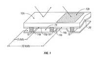
- FIG. 1is an isometric view depicting a portion of one embodiment of an interferometric modulator display in which a movable reflective layer of a first interferometric modulator is in a relaxed position and a movable reflective layer of a second interferometric modulator is in an actuated position.
- FIG. 2is a system block diagram illustrating one embodiment of an electronic device incorporating a 3 ⁇ 3 interferometric modulator display.
- FIG. 3is a diagram of movable mirror position versus applied voltage for one exemplary embodiment of an interferometric modulator of FIG. 1 .
- FIG. 4is an illustration of a set of row and column voltages that may be used to drive an interferometric modulator display.
- FIG. 5Aillustrates one exemplary frame of display data in the 3 ⁇ 3 interferometric modulator display of FIG. 2 .
- FIG. 5Billustrates one exemplary timing diagram for row and column signals that may be used to write the frame of FIG. 5A .
- FIGS. 6A and 6Bare system block diagrams illustrating an embodiment of a visual display device comprising a plurality of interferometric modulators.
- FIG. 7Ais a cross section of the device of FIG. 1 .
- FIG. 7Bis a cross section of an alternative embodiment of an interferometric modulator.
- FIG. 7Cis a cross section of another alternative embodiment of an interferometric modulator.
- FIG. 7Dis a cross section of yet another alternative embodiment of an interferometric modulator.
- FIG. 7Eis a cross section of an additional alternative embodiment of an interferometric modulator.
- FIG. 8is a cross-sectional illustration of an optical device for modulating the intensity of light from an interferometric reflector.
- FIG. 9is a cross-sectional illustration of fluids in an optical device in an actuated position.
- FIG. 10is a cross-sectional illustration of an optical device having a fluid cell with hydrophobic walls.
- FIG. 11is a cross-sectional illustration of an optical device having a fluid cell with water-neutral walls.
- FIG. 12is a cross-sectional illustration of an example electrode configuration for an optical device.
- FIG. 13is a cross-sectional illustration of an example electrode configuration for an optical device.
- FIG. 14is a cross-sectional illustration of an example electrode configuration for an optical device.
- FIG. 15is a cross-sectional illustration of an example electrode configuration for an optical device.
- FIG. 16is a cross-sectional illustration of an example selectively wettable surface in an optical device.
- FIG. 17is a cross-sectional illustration of another embodiment of an optical device for modulating the intensity of light from an interferometric reflector
- the following detailed descriptionis directed to certain specific embodiments of the invention.
- the inventioncan be embodied in a multitude of different ways.
- the embodimentsmay be implemented in any device that is configured to display an image, whether in motion (e.g., video) or stationary (e.g., still image), and whether textual or pictorial.
- the embodimentsmay be implemented in or associated with a variety of electronic devices such as, but not limited to, mobile telephones, wireless devices, personal data assistants (PDAs), hand-held or portable computers, GPS receivers/navigators, cameras, MP3 players, camcorders, game consoles, wrist watches, clocks, calculators, television monitors, flat panel displays, computer monitors, auto displays (e.g., odometer display, etc.), cockpit controls and/or displays, display of camera views (e.g., display of a rear view camera in a vehicle), electronic photographs, electronic billboards or signs, projectors, architectural structures, packaging, and aesthetic structures (e.g., display of images on a piece of jewelry).
- MEMS devices of similar structure to those described hereincan also be used in non-display applications such as in electronic switching devices.
- FIG. 1One interferometric modulator display embodiment comprising an interferometric MEMS display element is illustrated in FIG. 1 .
- the pixelsare in either a bright or dark state.
- the display elementIn the bright (“on” or “open”) state, the display element reflects a large portion of incident visible light to a user.
- the dark (“off” or “closed”) stateWhen in the dark (“off” or “closed”) state, the display element reflects little incident visible light to the user.
- the light reflectance properties of the “on” and “off” statesmay be reversed.
- MEMS pixelscan be configured to reflect predominantly at selected colors, allowing for a color display in addition to black and white.
- FIG. 1is an isometric view depicting two adjacent pixels in a series of pixels of a visual display, wherein each pixel comprises a MEMS interferometric modulator.
- an interferometric modulator displaycomprises a row/column array of these interferometric modulators.
- Each interferometric modulatorincludes a pair of reflective layers positioned at a variable and controllable distance from each other to form a resonant optical gap with at least one variable dimension.
- one of the reflective layersmay be moved between two positions. In the first position, referred to herein as the relaxed position, the movable reflective layer is positioned at a relatively large distance from a fixed partially reflective layer.
- the movable reflective layerIn the second position, referred to herein as the actuated position, the movable reflective layer is positioned more closely adjacent to the partially reflective layer. Incident light that reflects from the two layers interferes constructively or destructively depending on the position of the movable reflective layer, producing either an overall reflective or non-reflective state for each pixel.
- the depicted portion of the pixel array in FIG. 1includes two adjacent interferometric modulators 12 a and 12 b .
- a movable reflective layer 14 ais illustrated in a relaxed position at a predetermined distance from an optical stack 16 a , which includes a partially reflective layer.
- the movable reflective layer 14 bis illustrated in an actuated position adjacent to the optical stack 16 b.
- optical stack 16typically comprise several fused layers, which can include an electrode layer, such as indium tin oxide (ITO), a partially reflective layer, such as chromium, and a transparent dielectric.
- ITOindium tin oxide
- the optical stack 16is thus electrically conductive, partially transparent, and partially reflective, and may be fabricated, for example, by depositing one or more of the above layers onto a transparent substrate 20 .
- the partially reflective layercan be formed from a variety of materials that are partially reflective such as various metals, semiconductors, and dielectrics.
- the partially reflective layercan be formed of one or more layers of materials, and each of the layers can be formed of a single material or a combination of materials.
- the layers of the optical stack 16are patterned into parallel strips, and may form row electrodes in a display device as described further below.
- the movable reflective layers 14 a , 14 bmay be formed as a series of parallel strips of a deposited metal layer or layers (orthogonal to the row electrodes of 16 a , 16 b ) deposited on top of posts 18 and an intervening sacrificial material deposited between the posts 18 . When the sacrificial material is etched away, the movable reflective layers 14 a , 14 b are separated from the optical stacks 16 a , 16 b by a defined gap 19 .
- a highly conductive and reflective materialsuch as aluminum may be used for the reflective layers 14 , and these strips may form column electrodes in a display device.
- the gap 19remains between the movable reflective layer 14 a and optical stack 16 a , with the movable reflective layer 14 a in a mechanically relaxed state, as illustrated by the pixel 12 a in FIG. 1 .
- the capacitor formed at the intersection of the row and column electrodes at the corresponding pixelbecomes charged, and electrostatic forces pull the electrodes together.
- the movable reflective layer 14is deformed and is forced against the optical stack 16 .
- a dielectric layerwithin the optical stack 16 may prevent shorting and control the separation distance between layers 14 and 16 , as illustrated by pixel 12 b on the right in FIG. 1 .
- the behavioris the same regardless of the polarity of the applied potential difference. In this way, row/column actuation that can control the reflective vs. non-reflective pixel states is analogous in many ways to that used in conventional LCD and other display technologies.
- FIGS. 2 through 5Billustrate one exemplary process and system for using an array of interferometric modulators in a display application.
- FIG. 2is a system block diagram illustrating one embodiment of an electronic device that may incorporate aspects of the invention.
- the electronic deviceincludes a processor 21 which may be any general purpose single- or multi-chip microprocessor such as an ARM, Pentium®, Pentium II®, Pentium III®, Pentium IV®, Pentium® Pro, an 8051, a MIPS®, a Power PC®, an ALPHA®, or any special purpose microprocessor such as a digital signal processor, microcontroller, or a programmable gate array.
- the processor 21may be configured to execute one or more software modules.
- the processormay be configured to execute one or more software applications, including a web browser, a telephone application, an email program, or any other software application.
- the processor 21is also configured to communicate with an array driver 22 .
- the array driver 22includes a row driver circuit 24 and a column driver circuit 26 that provide signals to a display array or panel 30 .
- the cross section of the array illustrated in FIG. 1is shown by the lines 1 - 1 in FIG. 2 .
- the row/column actuation protocolmay take advantage of a hysteresis property of these devices illustrated in FIG. 3 . It may require, for example, a 10 volt potential difference to cause a movable layer to deform from the relaxed state to the actuated state. However, when the voltage is reduced from that value, the movable layer maintains its state as the voltage drops back below 10 volts.
- the movable layerdoes not relax completely until the voltage drops below 2 volts.
- a window of applied voltageabout 3 to 7 V in the example illustrated in FIG. 3 , within which the device is stable in either the relaxed or actuated state. This is referred to herein as the “hysteresis window” or “stability window.”
- the row/column actuation protocolcan be designed such that during row strobing, pixels in the strobed row that are to be actuated are exposed to a voltage difference of about 10 volts, and pixels that are to be relaxed are exposed to a voltage difference of close to zero volts.
- each pixelsees a potential difference within the “stability window” of 3-7 volts in this example.
- This featuremakes the pixel design illustrated in FIG. 1 stable under the same applied voltage conditions in either an actuated or relaxed pre-existing state. Since each pixel of the interferometric modulator, whether in the actuated or relaxed state, is essentially a capacitor formed by the fixed and moving reflective layers, this stable state can be held at a voltage within the hysteresis window with almost no power dissipation. Essentially no current flows into the pixel if the applied potential is fixed.
- a display framemay be created by asserting the set of column electrodes in accordance with the desired set of actuated pixels in the first row.
- a row pulseis then applied to the rob 1 electrode, actuating the pixels corresponding to the asserted column lines.
- the asserted set of column electrodesis then changed to correspond to the desired set of actuated pixels in the second row.
- a pulseis then applied to the row 2 electrode, actuating the appropriate pixels in row 2 in accordance with the asserted column electrodes.
- the row 1 pixelsare unaffected by the row 2 pulse, and remain in the state they were set to during the row 1 pulse. This may be repeated for the entire series of rows in a sequential fashion to produce the frame.
- the framesare refreshed and/or updated with new display data by continually repeating this process at some desired number of frames per second.
- protocols for driving row and column electrodes of pixel arrays to produce display framesare also well known and may be used in conjunction with the present invention.
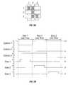
- FIGS. 4 , 5 A, and 5 Billustrate one possible actuation protocol for creating a display frame on the 3 ⁇ 3 array of FIG. 2 .
- FIG. 4illustrates a possible set of column and row voltage levels that may be used for pixels exhibiting the hysteresis curves of FIG. 3 .
- actuating a pixelinvolves setting the appropriate column to ⁇ V bias , and the appropriate row to + ⁇ V, which may correspond to ⁇ 5 volts and +5 volts, respectively. Relaxing the pixel is accomplished by setting the appropriate column to +V bias , and the appropriate row to the same + ⁇ V, producing a zero volt potential difference across the pixel.
- the pixelsare stable in whatever state they were originally in, regardless of whether the column is at +V bias , or ⁇ V bias .
- voltages of opposite polarity than those described abovecan be used, e.g., actuating a pixel can involve setting the appropriate column to +V bias , and the appropriate row to ⁇ V.
- releasing the pixelis accomplished by setting the appropriate column to ⁇ V bias , and the appropriate row to the same ⁇ V, producing a zero volt potential difference across the pixel.
- FIG. 5Bis a timing diagram showing a series of row and column signals applied to the 3 ⁇ 3 array of FIG. 2 which will result in the display arrangement illustrated in FIG. 5A , where actuated pixels are non-reflective.
- the pixelsPrior to writing the frame illustrated in FIG. 5A , the pixels can be in any state, and in this example, all the rows are at 0 volts, and all the columns are at +5 volts. With these applied voltages, all pixels are stable in their existing actuated or relaxed states.
- pixels (1,1), (1,2), (2,2), (3,2) and (3,3)are actuated.
- columns 1 and 2are set to ⁇ 5 volts, and column 3 is set to +5 volts. This does not change the state of any pixels, because all the pixels remain in the 3-7 volt stability window.
- Row 1is then strobed with a pulse that goes from 0, up to 5 volts, and back to zero. This actuates the (1,1) and (1,2) pixels and relaxes the (1,3) pixel. No other pixels in the array are affected.
- column 2is set to ⁇ 5 volts
- columns 1 and 3are set to +5 volts.
- Row 3is similarly set by setting columns 2 and 3 to ⁇ 5 volts, and column 1 to +5 volts.
- the row 3 strobesets the row 3 pixels as shown in FIG. 5A .
- the row potentialsare zero, and the column potentials can remain at either +5 or ⁇ 5 volts, and the display is then stable in the arrangement of FIG. 5A . It will be appreciated that the same procedure can be employed for arrays of dozens or hundreds of rows and columns.
- FIGS. 6A and 6Bare system block diagrams illustrating an embodiment of a display device 40 .
- the display device 40can be, for example, a cellular or mobile telephone.
- the same components of display device 40 or slight variations thereofare also illustrative of various types of display devices such as televisions, portable media players, and computers.
- the display device 40includes a housing 41 , a display 30 , an antenna 43 , a speaker 45 , an input device 48 , and a microphone 46 .
- the housing 41is generally formed from any of a variety of manufacturing processes as are well known to those of skill in the art, including injection molding and vacuum forming.
- the housing 41may be made from any of a variety of materials, including, but not limited to, plastic, metal, glass, rubber, and ceramic, or a combination thereof.
- the housing 41includes removable portions (not shown) that may be interchanged with other removable portions of different color, or containing different logos, pictures, or symbols.
- the display 30 of exemplary display device 40may be any of a variety of displays, including a bi-stable display, as described herein.
- the display 30includes a flat-panel display, such as plasma, EL, OLED, STN LCD, or TFT LCD as described above, or a non-flat-panel display, such as a CRT or other tube device, as is well known to those of skill in the art.
- the display 30includes an interferometric modulator display, as described herein.
- the components of one embodiment of exemplary display device 40are schematically illustrated in FIG. 6B .
- the illustrated exemplary display device 40includes a housing 41 and can include additional components at least partially enclosed therein.
- the exemplary display device 40includes a network interface 27 that includes an antenna 43 , which is coupled to a transceiver 47 .
- the transceiver 47is connected to a processor 21 , which is connected to conditioning hardware 52 .
- the conditioning hardware 52may be configured to condition a signal (e.g., filter a signal).
- the conditioning hardware 52is connected to a speaker 45 and a microphone 46 .
- the processor 21is also connected to an input device 48 and a driver controller 29 .
- the driver controller 29is coupled to a frame buffer 28 and to an array driver 22 , which in turn is coupled to a display array 30 .
- a power supply 50provides power to all components as required by the particular exemplary display device 40 design.
- the network interface 27includes the antenna 43 and the transceiver 47 so that the exemplary display device 40 can communicate with one or more devices over a network. In one embodiment, the network interface 27 may also have some processing capabilities to relieve requirements of the processor 21 .
- the antenna 43is any antenna known to those of skill in the art for transmitting and receiving signals. In one embodiment, the antenna transmits and receives RF signals according to the IEEE 802.11 standard, including IEEE 802.11(a), (b), or (g). In another embodiment, the antenna transmits and receives RF signals according to the BLUETOOTH standard. In the case of a cellular telephone, the antenna is designed to receive CDMA, GSM, AMPS, or other known signals that are used to communicate within a wireless cell phone network.
- the transceiver 47pre-processes the signals received from the antenna 43 so that they may be received by and further manipulated by the processor 21 .
- the transceiver 47also processes signals received from the processor 21 so that they may be transmitted from the exemplary display device 40 via the antenna 43 .
- the transceiver 47can be replaced by a receiver.
- network interface 27can be replaced by an image source, which can store or generate image data to be sent to the processor 21 .
- the image sourcecan be a digital video disc (DVD) or a hard-disc drive that contains image data, or a software module that generates image data.
- Processor 21generally controls the overall operation of the exemplary display device 40 .
- the processor 21receives data, such as compressed image data from the network interface 27 or an image source, and processes the data into raw image data or into a format that is readily processed into raw image data.
- the processor 21then sends the processed data to the driver controller 29 or to frame buffer 28 for storage.
- Raw datatypically refers to the information that identifies the image characteristics at each location within an image. For example, such image characteristics can include color, saturation, and gray-scale level.
- the processor 21includes a microcontroller, CPU, or logic unit to control operation of the exemplary display device 40 .
- the processor 21may also be configured to execute one or more software applications, including a web browser, a telephone application, an email program, or any other software application.
- Conditioning hardware 52generally includes amplifiers and filters for transmitting signals to the speaker 45 , and for receiving signals from the microphone 46 .
- Conditioning hardware 52may be discrete components within the exemplary display device 40 , or may be incorporated within the processor 21 or other components.
- the driver controller 29takes the raw image data generated by the processor 21 either directly from the processor 21 or from the frame buffer 28 and reformats the raw image data appropriately for high speed transmission to the array driver 22 . Specifically, the driver controller 29 reformats the raw image data into a data flow having a raster-like format, such that it has a time order suitable for scanning across the display array 30 . Then the driver controller 29 sends the formatted information to the array driver 22 .
- a driver controller 29such as a LCD controller, is often associated with the system processor 21 as a stand-alone Integrated Circuit (IC), such controllers may be implemented in many ways. They may be embedded in the processor 21 as hardware, embedded in the processor 21 as software, or fully integrated in hardware with the array driver 22 .
- the array driver 22receives the formatted information from the driver controller 29 and reformats the video data into a parallel set of waveforms that are applied many times per second to the hundreds and sometimes thousands of leads coming from the display's x-y matrix of pixels.
- driver controller 29is a conventional display controller or a bi-stable display controller (e.g., an interferometric modulator controller).
- array driver 22is a conventional driver or a bi-stable display driver (e.g., an interferometric modulator display).
- a driver controller 29is integrated with the array driver 22 .
- display array 30is a typical display array or a bi-stable display array (e.g., a display including an array of interferometric modulators).
- the input device 48allows a user to control the operation of the exemplary display device 40 .
- input device 48includes a keypad, such as a QWERTY keyboard or a telephone keypad, a button, a switch, a touch-sensitive screen, or a pressure- or heat-sensitive membrane.
- the microphone 46is an input device for the exemplary display device 40 . When the microphone 46 is used to input data to the device, voice commands may be provided by a user for controlling operations of the exemplary display device 40 .
- Power supply 50can include a variety of energy storage devices as are well known in the art.
- power supply 50is a rechargeable battery, such as a nickel-cadmium battery or a lithium ion battery.
- power supply 50is a renewable energy source, a capacitor, or a solar cell including a plastic solar cell, and solar-cell paint.
- power supply 50is configured to receive power from a wall outlet.
- control programmabilityresides, as described above, in a driver controller which can be located in several places in the electronic display system. In some embodiments, control programmability resides in the array driver 22 . Those of skill in the art will recognize that the above-described optimizations may be implemented in any number of hardware and/or software components and in various configurations.
- FIGS. 7A-7Eillustrate five different embodiments of the movable reflective layer 14 and its supporting structures.
- FIG. 7Ais a cross section of the embodiment of FIG. 1 , where a strip of metal material 14 is deposited on orthogonally extending supports 18 .
- FIG. 7Bthe moveable reflective layer 14 is attached to supports at the corners only, on tethers 32 .
- FIG. 7Cthe moveable reflective layer 14 is suspended from a deformable layer 34 , which may comprise a flexible metal.
- the deformable layer 34connects, directly or indirectly, to the substrate 20 around the perimeter of the deformable layer 34 .
- connection postsare herein referred to as support posts.
- the embodiment illustrated in FIG. 7Dhas support post plugs 42 upon which the deformable layer 34 rests.
- the movable reflective layer 14remains suspended over the gap, as in FIGS. 7A-7C , but the deformable layer 34 does not form the support posts by filling holes between the deformable layer 34 and the optical stack 16 . Rather, the support posts are formed of a planarization material, which is used to form support post plugs 42 .
- the embodiment illustrated in FIG. 7Eis based on the embodiment shown in FIG. 7D , but may also be adapted to work with any of the embodiments illustrated in FIGS. 7A-7C , as well as additional embodiments not shown. In the embodiment shown in FIG. 7E , an extra layer of metal or other conductive material has been used to form a bus structure 44 . This allows signal routing along the back of the interferometric modulators, eliminating a number of electrodes that may otherwise have had to be formed on the substrate 20 .
- the interferometric modulatorsfunction as direct-view devices, in which images are viewed from the front side of the transparent substrate 20 , the side opposite to that upon which the modulator is arranged.
- the reflective layer 14optically shields the portions of the interferometric modulator on the side of the reflective layer opposite the substrate 20 , including the deformable layer 34 . This allows the shielded areas to be configured and operated upon without negatively affecting the image quality.
- Such shieldingallows the bus structure 44 in FIG. 7E , which provides the ability to separate the optical properties of the modulator from the electromechanical properties of the modulator, such as addressing and the movements that result from that addressing.
- This separable modulator architectureallows the structural design and materials used for the electromechanical aspects and the optical aspects of the modulator to be selected and to function independently of each other.
- the embodiments shown in FIGS. 7C-7Ehave additional benefits deriving from the decoupling of the optical properties of the reflective layer 14 from its mechanical properties, which are carried out by the deformable layer 34 .
- Thisallows the structural design and materials used for the reflective layer 14 to be optimized with respect to the optical properties, and the structural design and materials used for the deformable layer 34 to be optimized with respect to desired mechanical properties.
- an interferometric optical stackcomprising a reflective layer and a partially reflective, partially transmissive layer can be provided. These layers can be relatively fixed in relationship to one another, resulting in a relatively constant set of wavelengths of light reflected by the interferometric optical stack. Light reflected by the interferometric optical stack can then be modulated using actionable fluids which can be configured to block incident light or allow it to pass through to the interferometric optical stack.
- embodimentscan use the phenomenon of electrowetting where the hydrophilicity of one or more surfaces is changed by applying an electrical field.
- An interferometric optical stackcan be built on a sealed cavity which, in some embodiments, contains a hydrophobic black fluid (oil) and water.
- the one or more surfacesare assumed to be hydrophobic such that the black dye spreads out to occlude a relatively large portion of the interferometric optical stack, resulting in relatively low intensity reflection of incident light.
- the one or more surfacesbecome hydrophilic, the black dye beads up and occludes a relatively small portion of the interferometric optical stack, resulting in higher intensity reflection.
- lightcan be selectively modulated, where selective modulation includes binary state (on/off) modulation, or modulation in an analog manner with continuously variable light modulation, as described further herein.
- FIG. 8is a cross-sectional schematic representation of an optical device 800 .
- the optical device 800comprises an at least partially optically transmissive first surface 812 and an optical stack 822 spaced from the first surface 812 .
- the optical stack 822comprises a reflective first layer 804 and a partially reflective, partially transmissive second layer 808 .
- the optical stack 822is adapted to reflect light having a set of wavelengths (e.g., visible wavelengths) determined by interference of light reflected from the first layer 804 and the second layer 808 .
- the optical device 800further comprises a first fluid 814 between the first surface 812 and the optical stack 822 .
- the optical device 800further comprises a second surface 818 between the first surface 812 and the optical stack 822 .
- the second surface 818can be located anywhere between the first surface 812 and the optical stack 822 .
- the device 800may include more than one instance of the second surface 818 .
- the first fluid 814covers a first portion of the second surface 818 when a first voltage is applied to the device 800 .
- the first fluid 814covers a second portion of the second surface 818 when a second voltage is applied to the device 800 .
- the first surface 812 and the optical stack 822define at least a portion of the boundary of a fluid cell 824 , as discussed more fully below.
- the optical device 800can be combined with other like devices to form a display for an electronic device such as a cell phone or laptop computer.
- the optical device 800represents a pixel or sub-pixel of such a display.
- Two useful characteristics of an optical device for use in a displayare the capability to present a selected color to a viewer (e.g. red, green, blue, etc.), as well as to modulate the intensity of the light seen by the viewer.
- the optical device 800can perform these two functions with the optical stack 822 and the fluid cell 824 , respectively.
- Optical devices with these capabilitiescan be combined in various ways to form displays capable of presenting thousands of colors and grayscales.
- the intensity of light reflected from each optical device 800 within the displaycan also be modulated in patterns which can form graphical content on the display, such as still images or video.
- the optical stack 822can be configured to display a selected color, or range of colors, by taking advantage of optical interference effects to reflect visible light of certain wavelengths without reflecting visible light of other wavelengths.
- the optical stack 822can also be configured to modulate non-visible light such as infrared or UV light.
- the optical stack 822is an optically resonant cavity similar to a Fabry-Perot etalon.
- the optical stack 822comprises a partially reflective, partially optically transmissive layer 808 separated from an optically reflective layer 804 (each of which acts as one mirror of an optically resonant cavity), both generally residing on a substrate 802 .
- the partially reflective, partially transmissive layer 808can also serve as an optical absorber which can provide for a narrower band of wavelengths reflected by the optical stack 822 .
- the partially reflective, partially transmissive layer 808comprises a layer of chromium, germanium, or molybdenum.
- the optically reflective layer 804can comprise aluminum. Other materials for these two layers are also suitable.
- one or both of the partially reflective, partially transmissive layer 808 and the reflective layer 804can comprise multiple sub-layers of different materials.
- the partially reflective, partially transmissive layer 808 and the reflective layer 804can be separated by an air gap, but in other embodiments, they are separated by a substantially optically transmissive dielectric layer 806 (e.g. silicon dioxide).
- a substantially optically transmissive dielectric layer 806e.g. silicon dioxide.
- the use of the dielectric material to separate the reflective layer 804 from the partially reflective, partially transmissive layer 808can, in some cases, help prevent gap variations which can compromise the optical performance of the optical device 800 . These gap variations can be caused by tilt or curvature of the two surfaces 804 and 808 which may result during fabrication of the device 800 and/or may gradually occur over time.
- the dielectric layer 806may comprise several sub-layers of dielectric materials with different refractive indexes.
- the dielectric layer 806may comprise alternating layers of dielectric materials with relatively higher and relatively lower refractive indexes. These dielectric sub-layers can be designed to improve certain optical characteristics of the optical device 800 in ways which are known in the
- the optical stack 822When light is incident upon the optical stack 822 , it is reflected to some degree both from the partially reflective, partially transmissive layer 808 and from the reflective layer 804 .
- the separation between layers 804 and 808defining a height of an optical cavity between the two layers 804 , 808
- the refractive index of the dielectric layer 806light of certain wavelengths reflecting from the partially reflective, partially transmissive layer 808 will be slightly out of phase with the light reflecting from the reflective layer 804 . Based on the phase difference, some wavelengths will constructively interfere, while others will destructively interfere.
- the height of the optical cavitymay be such that red wavelengths have a phase difference which leads to constructive interference, while green and blue wavelengths have a phase difference which leads to destructive interference.
- the thickness and type of material, with its associated refractive index, used to form the dielectric layer 806can be altered to tune the reflection of the optical stack 822 to a specific range of visible wavelengths which are interpreted by the human eye as a desired color.
- the dielectric layer 806can have a thickness that corresponds to approximately one half of a wavelength, in the dielectric layer 806 , of a selected wavelength of visible light which the optical stack 822 is configured to reflect.
- a number of optical devices 800tuned to reflect various visible wavelengths of light, can be assembled in various ways to form a display capable of reproducing thousands of colors.
- the intensity of light reflected from each optical device 800can be modulated using the fluid cell 824 , as described below.
- the fluid cell 824can be used to modulate the intensity of the light reflected by the optical stack 822 .
- the fluid cell 824includes a perimeter wall 810 , two portions of which are illustrated in the cross-section of FIG. 8 .
- the perimeter wall 810defines at least a portion of the boundary of a cavity which contains one or more fluids and is capped by the optically transmissive upper surface 812 .
- the cavity formed by the perimeter wall 810can be filled with two different fluids (e.g., liquids) 814 and 816 , which are non-soluble in one another so as to remain substantially separated from one another.
- the two fluids 814 and 816have differing optical characteristics.
- fluid 814can absorb visible light, whether uniformly across the visible spectrum or preferentially at selected wavelengths, while fluid 816 can be substantially optically transmissive.
- fluid 814will be referred to as the absorbent fluid
- fluid 816will be referred to as the transmissive fluid, with the understanding that, in certain embodiments of the invention, other optical characteristics of fluids within the fluid cell 824 may be emphasized other than their relative transmissivity to visible light.
- the transmissive fluid 816can comprise many different materials.
- the transmissive fluid 816may comprise water.
- the optically transmissive fluid 816may comprise ionic materials dissolved in water.
- the ionic materialsmay be inorganic (e.g. NaCl, KCl, etc.) or organic (e.g. sodium acetate, etc.).
- Other embodimentscould use other types of polar liquids with or without dissolved ionized species to make the transmissive liquid 816 electrically conductive.
- alcoholssuch as ethanol and glycerol could be used.
- Other types of optically transmissive fluidsare also suitable.
- the absorptive fluid 814can comprise several different materials.
- the absorptive fluid 814can be a non-polar liquid that is non-soluble in water.
- Suitable non-polar liquidscan include oils, hydrocarbons, esters, and ethers. If the material used for the absorptive fluid 814 is not naturally absorptive to visible wavelengths of light, any type of suitable dye can be added to the material to form the absorptive liquid 814 .
- a mixture of red, green, and blue dyescan be dissolved in the absorptive fluid 814 to tailor the fluid's absorptive properties.
- red, green, and blue dyescan be added in proportions that make the absorptive fluid 814 substantially equally absorptive to all visible wavelengths.
- the absorptive fluid 814can be tailored to preferentially absorb a specific range of visible wavelengths that are reflected by the optical stack 822 .
- the absorptive fluid 814can be tailored to absorb some other set of visible wavelengths.
- the fluid cell 824can also include the second surface 818 .
- This second surface 818can be formed anywhere inside the fluid cell 824 . In FIG. 8 , it is shown adjacent the optical stack 822 , but it can also be formed adjacent the optically transmissive upper surface 812 .
- the fluid cell 824includes more than one instance of the second surface 818 .
- one or more other layers of materiale.g. an electrode
- the partially reflective, partially transmissive layer 808can be particularly susceptible to harmful effects of moisture due to the thinness of this layer.
- the second surface 818 , and/or a material between the second surface 818 and the optical stack 822can act as a moisture barrier to help prevent fluid from the fluid cell 824 from corroding portions of the optical stack 822 .
- a layer of material between the second surface 818 and the optical stack 822can be made sufficiently thick and/or without significant structural defects such that fluid from the fluid cell 824 does not pose a significant corrosive hazard to portions of the optical stack 822 over a selected lifetime of the optical device 800 .
- the second surface 818is selectively wettable by the absorptive fluid 814 , the transmissive fluid 816 , or both the absorptive fluid 814 and the transmissive fluid 816 .
- the optical device 800includes a mechanism for controlling and modulating the relative portions of the second surface 818 that are covered, or wetted, by each of the two fluids within the fluid cell 824 .
- the optical device 800is configured so that the absorptive fluid 814 covers all or a majority of the second surface 818 . In this configuration, a light ray 820 incident upon the optical device 800 can pass through the optically transmissive upper surface 812 as well as the transmissive fluid 816 .
- the absorptive fluid 814can be chosen to substantially absorb the light ray 820 before it reaches the optical stack 822 . Whether or not the light ray 820 is absorbed by the absorptive fluid 814 will depend upon the absorptive characteristics of the absorptive fluid 814 , the spectral transmissivities of the transmissive fluid 816 and the upper surface 812 , and the wavelengths of the light ray 820 . For the case of a white incident light ray 820 , and an absorptive fluid that absorbs all or most visible wavelengths of light, very little visible light incident upon the optical device 800 will be reflected by the optical stack 822 to a viewer.
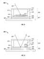
- the optical device 900is configured, via a controllable mechanism, (examples of which are described below) so that the absorptive fluid 914 only covers a small portion of the second surface 918 .
- an incident light ray 920can pass through the optically transmissive upper surface 912 , through the transmissive fluid 916 , and to the optical stack 922 .
- the nature of the reflection from the optical stack 922depends upon the configuration of the stack as described above.
- the optical stack 922can be designed to reflect red, green, blue, or some other color of light. If for example, the optical stack 922 is designed to reflect red light and the incident ray 920 consists of white light, then the reflected ray of light 921 seen by a viewer will appear red.
- the ability to selectively modulate the wettability of relative portions of the second surface 918 that are covered by the absorptive 914 and transmissive 916 fluidsadvantageously allows for the creation of a variable aperture through which light incident upon the optical device 900 can be reflected.
- the “open” portion of the variable apertureis relatively large, allowing for the reflection of a significant portion of light that is incident upon the optical device 900 and placing the optical device 900 in a “bright” state.
- the “open” portion of the variable apertureis small, such that the aperture is practically entirely closed, placing the optical device 800 in a “dark” state. While FIGS.
- variable aperture formed by the absorptive 814 and transmissive 816 fluidsis either practically fully open or fully closed, there is a continuous range of intermediate states between these two extremes. In this way, the intensity of light reflected by the optical stack 822 can be modulated in an analog-type manner.
- One way of controlling the relative portions of the second surface 818 that are covered by each of the absorptive 814 and transmissive 816 fluidsis to use the phenomenon of electrowetting.
- one of the two fluids 814 and 816 in the fluid cell 824has a greater affinity for the second surface 818 than the other.
- the fluid with the greater affinity for the second surface 818will displace the other fluid and cover, or wet, at least a portion of the second surface 818 .
- the portion of the second surface 818 that is covered by the fluid with the greater affinity for the second surfacecan depend on several factors, including the volume of the fluid and the degree of its affinity for the second surface 818 .
- the volume of the fluid whose affinity for the second surface 818is sufficiently large, it can cover substantially the entire second surface 818 .
- the absorptive fluid 814is taken as having a greater affinity for the second surface 818 than the transmissive fluid 816 and covers substantially the entire second surface 818 .
- the orientation of the fluids 814 and 816 shown in FIG. 8is generally stable because it represents a low energy state of the fluid cell 822 system.
- the energy balancecan be disturbed by applying an electric field to the system.
- the liquid whose affinity for the second surface 818 is initially lesscan be made to displace the fluid whose affinity for the surface 818 is initially greater. This can be done, for example, by applying a voltage across a pair of electrodes on either side of the second surface 818 .
- a portion of the optical stack 822can serve as one electrode.
- an electrically conductive portion of the optical stack 822can be used as an electrode for the fluid cell 824 such that one separate electrode for the fluid cell 824 can be omitted.
- the transmissive upper surface 812can comprise indium tin oxide (ITO) or some other optically transmissive conductor, and can serve as another electrode. Other electrode configurations will be described below.
- one of the fluids 814 and 816will be an electrical conductor, while the other will be substantially electrically insulative.
- one electrodecan be in electrical communication with the fluid that is electrically conductive.
- the optically transmissive fluid 816is a water-based electrolyte that is electrically conductive
- the absorptive fluid 814is an oil-based absorptive fluid that is an electrical insulator.
- the second surface 818can be an electrical insulating, hydrophobic material such as a fluoropolymer.
- the oil-based absorptive fluid 814has a greater affinity for the second surface 818 than does the water-based transmissive fluid 816 .
- the stable low-energy state of the device 800is as shown in FIG. 8 , where the oil-based absorptive fluid 814 covers a substantial portion of the second surface 818 .
- the energy balance of the device 800can be upset, causing the water-based transmissive fluid 816 to displace the oil-based absorptive fluid 814 .
- the resulting configurationis illustrated in FIG. 9 where the oil-based absorptive fluid 914 is beaded up and the second surface 918 is covered to a greater extent by the water-based transmissive fluid 916 .
- This mechanismcan be understood by considering that the overall energy of the device 900 can be minimized, once a voltage has been applied to it, by reconfiguring itself so that electrical charges within the electrically conductive water-based electrolyte minimize their separation from charges of the opposite sign on the other side of the hydrophobic second surface 918 .
- the thickness of material between the second surface 818 and the optical stack 822can be selected with respect to the electrical performance of the optical device 800 , the moisture blocking characteristics of the material, or both of these considerations.
- a thinner layer of material between the second surface 818 and the optical stack 822can result in greater responsiveness of the transmissive fluid 816 and the absorptive fluid 814 for a given voltage applied to the optical device 800 .
- a thicker layer of material between the second surface 818 and the optical stack 822can result in an improved moisture barrier between the fluid cell 824 and the optical stack 822 without significant degradation in the electrical performance of the device 800 .
- the thickness of material between the second surface 818 and the optical stack 822can be selected based on some other consideration, such as the impact of the thickness of the material on the optical performance of the device 800 .
- the second surface 818comprise hydrophobic material but the perimeter wall of the fluid cell 824 can also be made to be hydrophobic.
- FIG. 10shows the optical device 800 in an un-actuated state 1030 as well as an actuated state 1032 .
- the perimeter wall 1010comprises hydrophobic material
- the oil-based absorptive fluid 1014may tend to have a concave profile in the stable, un-actuated state 1030 .
- the perimeter wallis hydrophilic and the oil-based absorptive fluid 814 may tend toward a more convex profile, as shown in FIG. 8 ).
- the oil-based absorptive fluid 1014may tend to adhere to the perimeter wall 1010 of the fluid cell, as shown in FIG. 10 , which can be beneficial in some applications.
- FIG. 11illustrates the optical device 800 in an un-actuated state 1130 , where the perimeter wall 1110 of the fluid cell 824 is water-neutral.
- the oil-based absorptive fluid 1114may tend toward a more planar profile in the stable, un-actuated state.
- the planar profile of the oil-based absorptive fluid 1114 in this type of embodimentcan be beneficial in certain cases because it can result in more uniform absorption of light incident upon the optical device 800 .
- the thickness of the layer of absorptive fluid 1114is relatively uniform over the lower surface of the fluid cell 824 , the amount of light absorbed by the absorptive fluid 1114 will also tend to be relatively uniform for light incident upon it, regardless of the precise point of incidence upon the absorptive fluid 1114 .
- the second surface 818could be hydrophilic rather than hydrophobic.
- the second surface 818could exhibit neutral wetting properties towards water and a hydrophobic fluid, and the relative affinities of the fluids for the second surface 818 could be based on some other characteristic.
- FIGS. 12-15illustrate various electrode configurations which can be used in various embodiments. Additional electrode configurations will also be apparent to those skilled in the art based upon these figures.
- a portion of the optical stack 822could serve as an electrode in some embodiments.
- the reflective layer 804 and the partially reflective, partially transmissive layer 808 of the optical stack 822can be made of aluminum and chromium, respectively. In these embodiments, either layer could serve as an electrode.
- the dielectric layer 806could function as an electrode if it is formed from an optically transmissive, electrically conductive material, such as ITO.
- the reflective layer 804 , the partially reflective, partially transmissive layer 808 , and/or the dielectric layer 806can serve dual functions; each layer can contribute to the optical performance of the optical stack 822 as well as the electrical performance of the fluid cell 824 .
- This overlapping functionality between portions of the optical stack 822 and the fluid cell 824can allow for fewer structures and/or components in the optical device 800 and can result in a compact design.
- the overlapping functionality between portions of the optical stack 822 and the fluid cell 824can result in improved performance of the optical device 800 (e.g. speed, efficiency, etc.) that typically result from reduced dimensions in electrical and optical devices.
- FIG. 12illustrates another embodiment where a separate electrode 1240 is formed upon a substrate 1202 underneath the optical stack 1222 .
- Such embodimentscan provide the advantage of selecting the electrode 1240 material based upon its electrical characteristics, rather than basing the selection at least partially upon its optical characteristics, because the electrode 1240 does not lie in the optical path of light that is incident upon the optical device 1200 .
- the transmissive first surface 1212 of the optical device 1200serves as a second electrode.
- This second electrodecan be formed from an optically transmissive conductive material, such as ITO, so as to avoid any deleterious effects on the optical performance of the device 1200 by the electrode 1212 .
- FIG. 13illustrates another electrode configuration that can be used in some embodiments where the bottom electrode 1340 is located over the optical stack 1322 .
- This locationplaces the electrode 1340 in the optical path of light that is incident upon the optical device 1300 . Therefore, in some embodiments, the electrode 1340 may comprise an optically transmissive electrical conductor.
- the electrode 1340is nearer the fluid cell 1324 , which, in some cases, can allow for stronger electrical interactions between the electrode 1340 and the fluid cell 1324 for a given voltage than might otherwise be possible with the configuration shown in FIG. 12 .
- FIG. 14illustrates an electrode configuration where an upper electrode 1442 is located within the fluid cell 1424 .
- the electrodeis a ring (e.g., a polygonal ring, such as a rectangular ring or a hexagonal ring) inside the fluid cell 1424 , shown in cross-section in FIG. 14 .
- a possible advantage of this type of embodimentis that it allows a material to be chosen for the first surface 1412 of the fluid cell 1424 without the constraint that the material act as an electrical conductor.
- the material for the upper surface 1412 of the fluid cell 1424can be chosen primarily with regard to the material's optical characteristics, rather than electrical characteristics. Many variations on this configuration will be apparent to those skilled in the art.
- the perimeter wall of the fluid cell 1424could be formed out of electrically conductive material, allowing the wall itself to serve as an electrode.
- FIG. 15is illustrative of an embodiment which can be practiced with many different electrode configurations to influence the end location of the absorptive fluid 1514 when the optical device 1500 is in an actuated state.
- the bottom electrode 1540is positioned nearer one side of the optical device 1500 , offset with respect to electrode 1512 , so that electrical charges within the electrically conductive transmissive fluid 1516 will become concentrated nearer the bottom electrode 1540 , displacing the absorptive insulating fluid 1514 toward the side of the optical device 1500 in a predictable manner.
- the electrode material, size, shape, and positioncan be selected to cause the fluids 1514 and 1516 within the fluid cell 1524 to actuate in desirable, predictable ways.
- FIG. 16indicates a second type of mechanism which can be used in certain embodiments.
- Inlay 1630shows a magnified view of the second surface 1618 of the optical device 1600 which reveals that the surface comprises molecular chains.
- Inlay 1630illustrates the molecular chains in an un-actuated state, while inlay 1632 illustrates the molecular chains in an actuated state.
- Each molecular chaincan include a head portion 1652 and a tail portion 1650 .
- the head portions 1652can be hydrophilic, while the tail portions can be hydrophobic.
- Known surfactantsprovide examples of this type of molecular chains.
- the head portions 1652can be electrically charged. When a voltage is applied across two device electrodes, the orientation of the molecular chains can be altered so as to form a hydrophobic surface or a hydrophilic surface. For example, when a lower electrode 1640 is grounded, the hydrophilic head portions 1652 of the molecular chains can be presented to the interior of the fluid cell of the optical device 1600 . This configuration can tend to make the second surface 1618 have hydrophilic characteristics on a macroscopic scale, resulting in the displacement of an oil-based absorptive fluid 1614 by a water-based transmissive fluid 1616 .
- the second surface 1618can be made to display a hydrophobic characteristic on a macroscopic scale, resulting in the formation of an oil-based absorptive fluid 1614 layer spread over the second surface 1618 .
- the dominant phenomenon in this caseis not that the application of a voltage to the device electrodes upsets the energy balance of the fluid cell system to re-orient the fluids 1614 and 1616 .
- the very nature of the second surface 1618is altered between hydrophobic and hydrophilic states, or anywhere in between, which in turn causes the fluids 1614 and 1616 to become re-oriented and provide modulation of light incident upon the optical device 1600 .
- fabrication of the optical devicecan be done using techniques, such as photolithography, which are known in the art.
- a substrate 802can be provided.
- An electrode and optical stack 822can then be formed upon the substrate 802 .
- the perimeter wall of the fluid cell 824 and the second surface 818can be formed.
- the fluid cell 824can be filled with the absorptive fluid 814 as well as the transmissive fluid 816 and the cell can be capped and sealed by the transmissive first surface 812 .
- the optical device 800can also be fabricated by forming the optical stack 822 on a first substrate 802 and forming the fluid cell 824 on a second substrate (not shown). The first and second substrates can then be fixed in proximity to one another to form the optical device 800 .
- a plurality of optical devices 800can be formed on the substrate 802 to create displays which incorporate a plurality of pixels.
- pixels of different colorscan be achieved by altering the thickness of the dielectric layer 806 at different locations on a substrate 802 to achieve a desired wavelength range of reflectivity of the corresponding optical stacks 822 at those locations.
- red, green, and blue pixelsfor example, can be formed on the substrate 802 .
- portions of the optical stack 822can function as electrodes in some embodiments. A plurality of these electrodes can be interconnected to form an electrical bus.
- a portion of the optical stack 822comprises an electrode, it can be advantageous to use the partially reflective, partially transmissive layer 808 as the electrode due to its close proximity to the fluid cell 824 . The closer proximity of the electrode can result in improved responsiveness of the fluids within the fluid cell 824 for a selected voltage.
- the relatively small thickness of the partially reflective, partially transmissive layer 808can result in relatively high electrical resistances which may, in certain circumstances, limit the length of an electrical bus that comprises the partially reflective, partially transmissive layer 808 of several devices 800 and which could lengthen the response time (e.g., the RC time constant) of the device to applied voltages.
- the reflective layer 804can be made with a greater thickness than the partially reflective, partially transmissive layer 806 , since it need not be partially optically transmissive. Therefore, in some embodiments, an electrical bus can be formed by interconnecting the reflective layers 804 from each of a plurality of optical devices 800 . In addition, to maintain the advantages of an electrode which is in closer proximity to the fluid cell 824 of each of the plurality of optical devices 800 , vias can be formed to electrically connect the partially reflective, partially transmissive layer 808 and the reflective layer 804 of each of the plurality of optical devices 800 .
- Such viascan be formed according to any technique known in the art and can be positioned between separate ones of the plurality of optical devices 800 , or underneath the perimeter walls 910 of the optical devices 800 , to reduce their impact upon the optical performance of the optical stack 822 of each of the optical devices 800 .
- Other positions for the interconnecting vias between the partially reflective, partially transmissive layer 808 and the reflective layer 804are also possible.
- the layers 804 , 806 in certain embodiments described hereincan be in electrical communication with one another to advantageously provide electrical conductivity to an electrode of the fluid cell 824 .
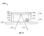
- FIG. 17illustrates another embodiment of the optical device of FIG. 8 .
- Optical device 1700can be considered as an inverted version of optical device 800 .
- a light ray 1720is incident upon, and passes through, the substrate 1702 .
- the substrate 1702can preferably comprise an optically transmissive material such as glass.
- the ray 1720passes through the transmissive fluid 1716 and reflects from the optical stack 1722 in a ray 1721 directed toward a viewer.
- the operation of the optical device 1700is analogous to what has been described with respect to optical device 800 . Fabrication, too, can be similarly done.
- a substrate 1702can be provided.
- an electrode 1718can be formed on the substrate 1702 .
- a perimeter wall 1710 of the fluid cell 1724can then be formed on the substrate 1702 or, in some cases, an electrode, of the form described with respect to FIG. 14 , can be incorporated into the perimeter wall 1710 .
- the cavity created by the formation of the fluid cell perimeter wall 1710can then be filled with a sacrificial material (e.g., Mo), and the layers of the optical stack 1722 can be formed on the resulting surface.
- a sacrificial materiale.g., Mo
- the sacrificial materialcan be removed (e.g., by etching with XeF2 flowed into an opening (not shown) in the fluid cell 1724 ) and the fluid cell 1724 can be filled with the absorptive 1714 and transmissive 1716 fluids. Finally, the fluid cell 1724 can be sealed.
- the optical device 1700can also be fabricated by forming the fluid cell 1724 on a first substrate 1702 and forming the optical stack 1722 on a second substrate (not shown). The first and second substrates can then be fixed in proximity to one another to form the optical device 1700 .
- an optical device(not shown) includes a fluid cell (e.g., 824 ) formed in proximity to a MEMS interferometric modulator.
- a fluid celle.g., 824
- a suitable MEMS interferometric modulatoris described herein and is illustrated, for example, in FIGS. 1 and 7 A- 7 E.
- the fluid cellcan be formed on the transparent substrate 20 on the side opposite the movable reflective layer 14 .
- An optical device of this sortcan modulate light with two mechanisms. For example, light incident upon the optical device can be modulated by movement of the movable reflective layer 14 and by movement of fluids within the fluid cell, as described herein.
- FIGS. 6A and 6Bare system block diagrams illustrating an embodiment of an electronic device which can incorporate a display 30 which comprises a plurality of optical devices as illustrated in FIGS. 8-17 .
- a potential advantageis that battery life in an electronic device which incorporates a display comprising optical devices of the sort illustrated in FIGS. 8-17 can be enhanced, compared to other types of displays, because the optical devices described herein only require power when the fluid cell system is actuated.
Landscapes
- Physics & Mathematics (AREA)
- General Physics & Mathematics (AREA)
- Optics & Photonics (AREA)
- Spectroscopy & Molecular Physics (AREA)
- Mechanical Light Control Or Optical Switches (AREA)
Abstract
Description
Claims (45)
Priority Applications (1)
| Application Number | Priority Date | Filing Date | Title |
|---|---|---|---|
| US11/776,490US8115987B2 (en) | 2007-02-01 | 2007-07-11 | Modulating the intensity of light from an interferometric reflector |
Applications Claiming Priority (2)
| Application Number | Priority Date | Filing Date | Title |
|---|---|---|---|
| US88779107P | 2007-02-01 | 2007-02-01 | |
| US11/776,490US8115987B2 (en) | 2007-02-01 | 2007-07-11 | Modulating the intensity of light from an interferometric reflector |
Publications (2)
| Publication Number | Publication Date |
|---|---|
| US20080186581A1 US20080186581A1 (en) | 2008-08-07 |
| US8115987B2true US8115987B2 (en) | 2012-02-14 |
Family
ID=39675902
Family Applications (1)
| Application Number | Title | Priority Date | Filing Date |
|---|---|---|---|
| US11/776,490Expired - Fee RelatedUS8115987B2 (en) | 2007-02-01 | 2007-07-11 | Modulating the intensity of light from an interferometric reflector |
Country Status (1)
| Country | Link |
|---|---|
| US (1) | US8115987B2 (en) |
Cited By (6)
| Publication number | Priority date | Publication date | Assignee | Title |
|---|---|---|---|---|
| US20110140996A1 (en)* | 2009-12-15 | 2011-06-16 | Lesley Anne Parry-Jones | Switchable transmissive/reflective electrowetting display |
| US20130342891A1 (en)* | 2012-06-26 | 2013-12-26 | Wintek Corporation | Electrowetting display device |
| US8693084B2 (en) | 2008-03-07 | 2014-04-08 | Qualcomm Mems Technologies, Inc. | Interferometric modulator in transmission mode |
| US8964280B2 (en) | 2006-06-30 | 2015-02-24 | Qualcomm Mems Technologies, Inc. | Method of manufacturing MEMS devices providing air gap control |
| US20160258812A1 (en)* | 2013-12-27 | 2016-09-08 | Panasonic Intellectual Property Management Co., Ltd. | Wavelength-variable optical filter module |
| US20190310456A1 (en)* | 2017-03-09 | 2019-10-10 | Boe Technology Group Co., Ltd. | Display panel and display device |
Families Citing this family (53)
| Publication number | Priority date | Publication date | Assignee | Title |
|---|---|---|---|---|
| US7629197B2 (en) | 2006-10-18 | 2009-12-08 | Qualcomm Mems Technologies, Inc. | Spatial light modulator |
| US7742220B2 (en) | 2007-03-28 | 2010-06-22 | Qualcomm Mems Technologies, Inc. | Microelectromechanical device and method utilizing conducting layers separated by stops |
| US7643202B2 (en) | 2007-05-09 | 2010-01-05 | Qualcomm Mems Technologies, Inc. | Microelectromechanical system having a dielectric movable membrane and a mirror |
| US7715085B2 (en) | 2007-05-09 | 2010-05-11 | Qualcomm Mems Technologies, Inc. | Electromechanical system having a dielectric movable membrane and a mirror |
| US7643199B2 (en) | 2007-06-19 | 2010-01-05 | Qualcomm Mems Technologies, Inc. | High aperture-ratio top-reflective AM-iMod displays |
| US7782517B2 (en) | 2007-06-21 | 2010-08-24 | Qualcomm Mems Technologies, Inc. | Infrared and dual mode displays |
| US7630121B2 (en) | 2007-07-02 | 2009-12-08 | Qualcomm Mems Technologies, Inc. | Electromechanical device with optical function separated from mechanical and electrical function |
| EP2183623A1 (en) | 2007-07-31 | 2010-05-12 | Qualcomm Mems Technologies, Inc. | Devices for enhancing colour shift of interferometric modulators |
| US8072402B2 (en) | 2007-08-29 | 2011-12-06 | Qualcomm Mems Technologies, Inc. | Interferometric optical modulator with broadband reflection characteristics |
| US7847999B2 (en) | 2007-09-14 | 2010-12-07 | Qualcomm Mems Technologies, Inc. | Interferometric modulator display devices |
| US7773286B2 (en) | 2007-09-14 | 2010-08-10 | Qualcomm Mems Technologies, Inc. | Periodic dimple array |
| US8058549B2 (en) | 2007-10-19 | 2011-11-15 | Qualcomm Mems Technologies, Inc. | Photovoltaic devices with integrated color interferometric film stacks |
| CN101828145B (en) | 2007-10-19 | 2012-03-21 | 高通Mems科技公司 | Displays with integrated photovoltaic elements |
| EP2203765A1 (en) | 2007-10-23 | 2010-07-07 | Qualcomm Mems Technologies, Inc. | Adjustably transmissive mems-based devices |
| US8941631B2 (en) | 2007-11-16 | 2015-01-27 | Qualcomm Mems Technologies, Inc. | Simultaneous light collection and illumination on an active display |
| US20090141334A1 (en)* | 2007-11-30 | 2009-06-04 | Motorola, Inc. | Electronic device housing having tunable metallic appearance |
| US7715079B2 (en) | 2007-12-07 | 2010-05-11 | Qualcomm Mems Technologies, Inc. | MEMS devices requiring no mechanical support |
| US8164821B2 (en) | 2008-02-22 | 2012-04-24 | Qualcomm Mems Technologies, Inc. | Microelectromechanical device with thermal expansion balancing layer or stiffening layer |
| US7612933B2 (en) | 2008-03-27 | 2009-11-03 | Qualcomm Mems Technologies, Inc. | Microelectromechanical device with spacing layer |
| US7898723B2 (en) | 2008-04-02 | 2011-03-01 | Qualcomm Mems Technologies, Inc. | Microelectromechanical systems display element with photovoltaic structure |
| US7969638B2 (en) | 2008-04-10 | 2011-06-28 | Qualcomm Mems Technologies, Inc. | Device having thin black mask and method of fabricating the same |
| US8023167B2 (en) | 2008-06-25 | 2011-09-20 | Qualcomm Mems Technologies, Inc. | Backlight displays |
| US7746539B2 (en) | 2008-06-25 | 2010-06-29 | Qualcomm Mems Technologies, Inc. | Method for packing a display device and the device obtained thereof |
| US7768690B2 (en) | 2008-06-25 | 2010-08-03 | Qualcomm Mems Technologies, Inc. | Backlight displays |
| US7859740B2 (en) | 2008-07-11 | 2010-12-28 | Qualcomm Mems Technologies, Inc. | Stiction mitigation with integrated mech micro-cantilevers through vertical stress gradient control |
| US7855826B2 (en) | 2008-08-12 | 2010-12-21 | Qualcomm Mems Technologies, Inc. | Method and apparatus to reduce or eliminate stiction and image retention in interferometric modulator devices |
| US8358266B2 (en) | 2008-09-02 | 2013-01-22 | Qualcomm Mems Technologies, Inc. | Light turning device with prismatic light turning features |
| EP2342595A1 (en)* | 2008-10-16 | 2011-07-13 | Miortech Holding B.V. | Electrowetting optical element arranged for preventing charge accumulation, and method for manufacturing an electrowetting optical element |
| EP2359170B1 (en) | 2008-11-13 | 2016-02-17 | Koninklijke Philips N.V. | Device for adaptable wavelength conversion and a solar cell |
| WO2010084200A1 (en)* | 2009-01-26 | 2010-07-29 | Seereal Technologies S.A. | Device for amplitude modulation |
| US8270056B2 (en) | 2009-03-23 | 2012-09-18 | Qualcomm Mems Technologies, Inc. | Display device with openings between sub-pixels and method of making same |
| CN102449512A (en) | 2009-05-29 | 2012-05-09 | 高通Mems科技公司 | Illumination devices and methods of fabrication thereof |
| TWI407146B (en)* | 2009-06-10 | 2013-09-01 | Ind Tech Res Inst | Electrowetting display and method for fabricating the same |
| US8270062B2 (en) | 2009-09-17 | 2012-09-18 | Qualcomm Mems Technologies, Inc. | Display device with at least one movable stop element |
| US8488228B2 (en) | 2009-09-28 | 2013-07-16 | Qualcomm Mems Technologies, Inc. | Interferometric display with interferometric reflector |
| GB0918959D0 (en)* | 2009-10-29 | 2009-12-16 | Liquavista Bv | Driving an electrowetting display device |
| KR20130100232A (en) | 2010-04-09 | 2013-09-10 | 퀄컴 엠이엠에스 테크놀로지스, 인크. | Mechanical layer of an electromechanical device and methods of forming the same |
| US8917438B2 (en)* | 2010-08-12 | 2014-12-23 | Creator Technology B.V. | Electronic color display using an electrowetting principle wherein the display comprises black matrix patterns that are aligned with a control means |
| CN103109315A (en) | 2010-08-17 | 2013-05-15 | 高通Mems科技公司 | Actuation and calibration of a charge neutral electrode in an interferometric display device |
| US9057872B2 (en) | 2010-08-31 | 2015-06-16 | Qualcomm Mems Technologies, Inc. | Dielectric enhanced mirror for IMOD display |
| CN103278922B (en)* | 2010-09-27 | 2016-05-18 | 薛英家 | Electrowetting Elements with Hydrophobic Walls |
| US8582115B2 (en)* | 2010-10-07 | 2013-11-12 | Omnivision Technologies, Inc. | Tunable and switchable multilayer optical devices |
| TW201217860A (en) | 2010-10-25 | 2012-05-01 | Ind Tech Res Inst | Cholesteric liquid crystal device |
| US8963159B2 (en) | 2011-04-04 | 2015-02-24 | Qualcomm Mems Technologies, Inc. | Pixel via and methods of forming the same |
| US9134527B2 (en) | 2011-04-04 | 2015-09-15 | Qualcomm Mems Technologies, Inc. | Pixel via and methods of forming the same |
| US8659816B2 (en) | 2011-04-25 | 2014-02-25 | Qualcomm Mems Technologies, Inc. | Mechanical layer and methods of making the same |
| US8736939B2 (en) | 2011-11-04 | 2014-05-27 | Qualcomm Mems Technologies, Inc. | Matching layer thin-films for an electromechanical systems reflective display device |
| WO2013162530A1 (en)* | 2012-04-25 | 2013-10-31 | Hewlett-Packard Development Company, L.P. | Cavity enhanced spectroscopy |
| JP2014164019A (en)* | 2013-02-22 | 2014-09-08 | Seiko Epson Corp | Wavelength variable interference filter, optical filter device, optical module, and electronic equipment |
| CN108021293B (en)* | 2016-10-28 | 2021-11-09 | 京东方科技集团股份有限公司 | Touch panel, sensing method thereof and display device |
| WO2019226439A1 (en)* | 2018-05-21 | 2019-11-28 | Corning Incorporated | Structures for laser bonding and liquid lenses comprising such structures |
| US12147030B2 (en)* | 2021-05-11 | 2024-11-19 | Ii-Vi Delaware, Inc. | Optical package having tunable filter |
| WO2023056074A1 (en)* | 2021-10-01 | 2023-04-06 | Solchroma Technologies, Inc. | Reflective display apparatus with optically absorptive fluid |
Citations (279)
| Publication number | Priority date | Publication date | Assignee | Title |
|---|---|---|---|---|
| US2590906A (en) | 1946-11-22 | 1952-04-01 | Farrand Optical Co Inc | Reflection interference filter |
| US2677714A (en) | 1951-09-21 | 1954-05-04 | Alois Vogt Dr | Optical-electrical conversion device comprising a light-permeable metal electrode |
| US3247392A (en) | 1961-05-17 | 1966-04-19 | Optical Coating Laboratory Inc | Optical coating and assembly used as a band pass interference filter reflecting in the ultraviolet and infrared |
| US3679313A (en) | 1970-10-23 | 1972-07-25 | Bell Telephone Labor Inc | Dispersive element for optical pulse compression |
| US3728030A (en) | 1970-06-22 | 1973-04-17 | Cary Instruments | Polarization interferometer |
| US3886310A (en) | 1973-08-22 | 1975-05-27 | Westinghouse Electric Corp | Electrostatically deflectable light valve with improved diffraction properties |
| US3955190A (en) | 1972-09-11 | 1976-05-04 | Kabushiki Kaisha Suwa Seikosha | Electro-optical digital display |
| US4403248A (en) | 1980-03-04 | 1983-09-06 | U.S. Philips Corporation | Display device with deformable reflective medium |
| US4421381A (en) | 1980-04-04 | 1983-12-20 | Yokogawa Hokushin Electric Corp. | Mechanical vibrating element |
| US4441789A (en) | 1980-03-31 | 1984-04-10 | Jenoptik Jena Gmbh | Resonance absorber |
| US4441791A (en) | 1980-09-02 | 1984-04-10 | Texas Instruments Incorporated | Deformable mirror light modulator |
| US4497974A (en) | 1982-11-22 | 1985-02-05 | Exxon Research & Engineering Co. | Realization of a thin film solar cell with a detached reflector |
| US4498953A (en) | 1983-07-27 | 1985-02-12 | At&T Bell Laboratories | Etching techniques |
| US4560435A (en) | 1984-10-01 | 1985-12-24 | International Business Machines Corporation | Composite back-etch/lift-off stencil for proximity effect minimization |
| US4655554A (en) | 1985-03-06 | 1987-04-07 | The United States Of America As Represented By The Secretary Of The Air Force | Spatial light modulator having a capacitively coupled photoconductor |
| US4705361A (en) | 1985-11-27 | 1987-11-10 | Texas Instruments Incorporated | Spatial light modulator |
| US4779959A (en)* | 1986-09-05 | 1988-10-25 | The Secretary Of State For Defence In Her Britannic Majesty's Government Of The United Kingdom Of Great Britain And Northern Ireland | Liquid crystal electro-optic modulator in a fabry-perot interferometer |
| US4786128A (en) | 1986-12-02 | 1988-11-22 | Quantum Diagnostics, Ltd. | Device for modulating and reflecting electromagnetic radiation employing electro-optic layer having a variable index of refraction |
| US4822993A (en) | 1987-02-17 | 1989-04-18 | Optron Systems, Inc. | Low-cost, substantially cross-talk free high spatial resolution 2-D bistable light modulator |
| US4859060A (en) | 1985-11-26 | 1989-08-22 | 501 Sharp Kabushiki Kaisha | Variable interferometric device and a process for the production of the same |
| US4925259A (en) | 1988-10-20 | 1990-05-15 | The United States Of America As Represented By The United States Department Of Energy | Multilayer optical dielectric coating |
| US4954789A (en) | 1989-09-28 | 1990-09-04 | Texas Instruments Incorporated | Spatial light modulator |
| US4956619A (en) | 1988-02-19 | 1990-09-11 | Texas Instruments Incorporated | Spatial light modulator |
| US4973131A (en) | 1989-02-03 | 1990-11-27 | Mcdonnell Douglas Corporation | Modulator mirror |
| US4982184A (en) | 1989-01-03 | 1991-01-01 | General Electric Company | Electrocrystallochromic display and element |
| US5022745A (en) | 1989-09-07 | 1991-06-11 | Massachusetts Institute Of Technology | Electrostatically deformable single crystal dielectrically coated mirror |
| US5028939A (en) | 1988-08-23 | 1991-07-02 | Texas Instruments Incorporated | Spatial light modulator system |
| US5062689A (en) | 1990-08-21 | 1991-11-05 | Koehler Dale R | Electrostatically actuatable light modulating device |
| US5091983A (en) | 1987-06-04 | 1992-02-25 | Walter Lukosz | Optical modulation apparatus and measurement method |
| US5096279A (en) | 1984-08-31 | 1992-03-17 | Texas Instruments Incorporated | Spatial light modulator and method |
| US5170283A (en) | 1991-07-24 | 1992-12-08 | Northrop Corporation | Silicon spatial light modulator |
| US5315370A (en) | 1991-10-23 | 1994-05-24 | Bulow Jeffrey A | Interferometric modulator for optical signal processing |
| US5381232A (en) | 1992-05-19 | 1995-01-10 | Akzo Nobel N.V. | Fabry-perot with device mirrors including a dielectric coating outside the resonant cavity |
| US5452138A (en) | 1991-07-31 | 1995-09-19 | Texas Instruments Incorporated | Deformable mirror device with integral color filter |
| US5471341A (en) | 1991-07-17 | 1995-11-28 | Optron Systems, Inc. | Membrane light modulating systems |
| EP0695959A1 (en) | 1994-07-29 | 1996-02-07 | AT&T Corp. | Direct view display based on a micromechanical modulator |
| US5526172A (en) | 1993-07-27 | 1996-06-11 | Texas Instruments Incorporated | Microminiature, monolithic, variable electrical signal processor and apparatus including same |
| US5550373A (en) | 1994-12-30 | 1996-08-27 | Honeywell Inc. | Fabry-Perot micro filter-detector |
| US5559358A (en) | 1993-05-25 | 1996-09-24 | Honeywell Inc. | Opto-electro-mechanical device or filter, process for making, and sensors made therefrom |
| US5561523A (en) | 1994-02-17 | 1996-10-01 | Vaisala Oy | Electrically tunable fabry-perot interferometer produced by surface micromechanical techniques for use in optical material analysis |
| US5597736A (en) | 1992-08-11 | 1997-01-28 | Texas Instruments Incorporated | High-yield spatial light modulator with light blocking layer |
| US5600383A (en) | 1990-06-29 | 1997-02-04 | Texas Instruments Incorporated | Multi-level deformable mirror device with torsion hinges placed in a layer different from the torsion beam layer |
| US5646768A (en) | 1994-07-29 | 1997-07-08 | Texas Instruments Incorporated | Support posts for micro-mechanical devices |
| US5646729A (en) | 1993-01-13 | 1997-07-08 | Vaisala Oy | Single-channel gas concentration measurement method and apparatus using a short-resonator Fabry-Perot interferometer |
| US5661592A (en) | 1995-06-07 | 1997-08-26 | Silicon Light Machines | Method of making and an apparatus for a flat diffraction grating light valve |
| US5665997A (en) | 1994-03-31 | 1997-09-09 | Texas Instruments Incorporated | Grated landing area to eliminate sticking of micro-mechanical devices |
| US5686979A (en)* | 1995-06-26 | 1997-11-11 | Minnesota Mining And Manufacturing Company | Optical panel capable of switching between reflective and transmissive states |
| US5699181A (en) | 1995-07-27 | 1997-12-16 | Samsung Electronics Co., Ltd. | Deformable mirror device and manufacturing method thereof |
| US5710656A (en) | 1996-07-30 | 1998-01-20 | Lucent Technologies Inc. | Micromechanical optical modulator having a reduced-mass composite membrane |
| US5719068A (en) | 1994-11-25 | 1998-02-17 | Semiconductor Energy Laboratory Co., Ltd. | Method for anisotropic etching conductive film |
| US5726805A (en)* | 1996-06-25 | 1998-03-10 | Sandia Corporation | Optical filter including a sub-wavelength periodic structure and method of making |
| US5734177A (en) | 1995-10-31 | 1998-03-31 | Sharp Kabushiki Kaisha | Semiconductor device, active-matrix substrate and method for fabricating the same |
| US5771116A (en) | 1996-10-21 | 1998-06-23 | Texas Instruments Incorporated | Multiple bias level reset waveform for enhanced DMD control |
| US5786927A (en) | 1997-03-12 | 1998-07-28 | Lucent Technologies Inc. | Gas-damped micromechanical structure |
| US5808781A (en) | 1996-02-01 | 1998-09-15 | Lucent Technologies Inc. | Method and apparatus for an improved micromechanical modulator |
| US5825528A (en) | 1995-12-26 | 1998-10-20 | Lucent Technologies Inc. | Phase-mismatched fabry-perot cavity micromechanical modulator |
| US5838484A (en) | 1996-08-19 | 1998-11-17 | Lucent Technologies Inc. | Micromechanical optical modulator with linear operating characteristic |
| US5867302A (en) | 1997-08-07 | 1999-02-02 | Sandia Corporation | Bistable microelectromechanical actuator |
| US5870221A (en) | 1997-07-25 | 1999-02-09 | Lucent Technologies, Inc. | Micromechanical modulator having enhanced performance |
| EP0879991A3 (en) | 1997-05-13 | 1999-04-21 | Matsushita Electric Industrial Co., Ltd. | Illuminating system |
| US5914804A (en) | 1998-01-28 | 1999-06-22 | Lucent Technologies Inc | Double-cavity micromechanical optical modulator with plural multilayer mirrors |
| US5920418A (en) | 1994-06-21 | 1999-07-06 | Matsushita Electric Industrial Co., Ltd. | Diffractive optical modulator and method for producing the same, infrared sensor including such a diffractive optical modulator and method for producing the same, and display device including such a diffractive optical modulator |
| US5961848A (en) | 1994-11-10 | 1999-10-05 | Thomson-Csf | Process for producing magnetoresistive transducers |
| US6028689A (en) | 1997-01-24 | 2000-02-22 | The United States Of America As Represented By The Secretary Of The Air Force | Multi-motion micromirror |
| US6031653A (en) | 1997-08-28 | 2000-02-29 | California Institute Of Technology | Low-cost thin-metal-film interference filters |
| US6040937A (en) | 1994-05-05 | 2000-03-21 | Etalon, Inc. | Interferometric modulation |
| US6046659A (en) | 1998-05-15 | 2000-04-04 | Hughes Electronics Corporation | Design and fabrication of broadband surface-micromachined micro-electro-mechanical switches for microwave and millimeter-wave applications |
| JP2000147262A (en) | 1998-11-11 | 2000-05-26 | Nobuyuki Higuchi | Converging device and photovoltaic power generation system utilizing the device |
| US6100861A (en) | 1998-02-17 | 2000-08-08 | Rainbow Displays, Inc. | Tiled flat panel display with improved color gamut |
| US6124851A (en) | 1995-07-20 | 2000-09-26 | E Ink Corporation | Electronic book with multiple page displays |
| US6242932B1 (en) | 1999-02-19 | 2001-06-05 | Micron Technology, Inc. | Interposer for semiconductor components having contact balls |
| US20010003487A1 (en) | 1996-11-05 | 2001-06-14 | Mark W. Miles | Visible spectrum modulator arrays |
| US6262697B1 (en) | 1998-03-20 | 2001-07-17 | Eastman Kodak Company | Display having viewable and conductive images |
| JP2001221913A (en) | 2000-02-08 | 2001-08-17 | Yokogawa Electric Corp | Fabry-Perot filter and infrared gas analyzer |
| JP2001249283A (en) | 2000-02-22 | 2001-09-14 | Marconi Communications Ltd | Wavelength selective optical filter |
| US6301000B1 (en) | 1999-01-11 | 2001-10-09 | Kenneth Carlisle Johnson | Dual-flexure light valve |
| US20010028503A1 (en) | 2000-03-03 | 2001-10-11 | Flanders Dale C. | Integrated tunable fabry-perot filter and method of making same |
| US20010043171A1 (en) | 2000-02-24 | 2001-11-22 | Van Gorkom Gerardus Gegorius Petrus | Display device comprising a light guide |
| US6323987B1 (en) | 1999-05-14 | 2001-11-27 | Agere Systems Optoelectronics Guardian Corp. | Controlled multi-wavelength etalon |
| US6327071B1 (en) | 1998-10-16 | 2001-12-04 | Fuji Photo Film Co., Ltd. | Drive methods of array-type light modulation element and flat-panel display |
| US6335235B1 (en) | 1999-08-17 | 2002-01-01 | Advanced Micro Devices, Inc. | Simplified method of patterning field dielectric regions in a semiconductor device |
| US20020015215A1 (en) | 1994-05-05 | 2002-02-07 | Iridigm Display Corporation, A Delaware Corporation | Interferometric modulation of radiation |
| US6351329B1 (en) | 1999-10-08 | 2002-02-26 | Lucent Technologies Inc. | Optical attenuator |
| JP2002062490A (en) | 2000-08-14 | 2002-02-28 | Canon Inc | Interferometric modulator |
| US20020024711A1 (en) | 1994-05-05 | 2002-02-28 | Iridigm Display Corporation, A Delaware Corporation | Interferometric modulation of radiation |
| US6356378B1 (en) | 1995-06-19 | 2002-03-12 | Reflectivity, Inc. | Double substrate reflective spatial light modulator |
| US6377233B2 (en) | 1998-10-08 | 2002-04-23 | International Business Machines Corporation | Micromechanical display and fabrication method |
| US6381022B1 (en) | 1992-01-22 | 2002-04-30 | Northeastern University | Light modulating device |
| US6384952B1 (en) | 1997-03-27 | 2002-05-07 | Mems Optical Inc. | Vertical comb drive actuated deformable mirror device and method |
| US20020054424A1 (en) | 1994-05-05 | 2002-05-09 | Etalon, Inc. | Photonic mems and structures |
| EP1205782A3 (en) | 2000-11-01 | 2002-05-29 | Agilent Technologies, Inc. (a Delaware corporation) | Optically tunable Fabry-Perot micro-electromechanical resonator |
| US6400738B1 (en) | 2000-04-14 | 2002-06-04 | Agilent Technologies, Inc. | Tunable Fabry-Perot filters and lasers |
| US20020070931A1 (en) | 2000-07-03 | 2002-06-13 | Hiroichi Ishikawa | Optical multilayer structure, optical switching device, and image display |
| JP2002221678A (en) | 2001-01-25 | 2002-08-09 | Seiko Epson Corp | Optical switching device, manufacturing method thereof, and image display device |
| US6433917B1 (en) | 2000-11-22 | 2002-08-13 | Ball Semiconductor, Inc. | Light modulation device and system |
| US6437583B1 (en) | 1996-02-14 | 2002-08-20 | Stmicroelectronics, Inc.. | Capacitive distance sensor |
| US6438282B1 (en) | 1998-01-20 | 2002-08-20 | Seiko Epson Corporation | Optical switching device and image display device |
| US6452712B2 (en) | 1995-12-01 | 2002-09-17 | Seiko Epson Corporation | Method of manufacturing spatial light modulator and electronic device employing it |
| US20020146200A1 (en) | 2001-03-16 | 2002-10-10 | Kudrle Thomas David | Electrostatically actuated micro-electro-mechanical devices and method of manufacture |
| US6466354B1 (en) | 2000-09-19 | 2002-10-15 | Silicon Light Machines | Method and apparatus for interferometric modulation of light |
| US20020149834A1 (en) | 2000-12-22 | 2002-10-17 | Ball Semiconductor, Inc. | Light modulation device and system |
| US20020149828A1 (en) | 1994-05-05 | 2002-10-17 | Miles Mark W. | Controlling micro-electro-mechanical cavities |
| US20020154422A1 (en) | 2001-04-23 | 2002-10-24 | Sniegowski Jeffry J. | Surface micromachined optical system with reinforced mirror microstructure |
| US20020197761A1 (en) | 2001-05-22 | 2002-12-26 | Reflectivity, Inc. | Method for making a micromechanical device by removing a sacrificial layer with multiple sequential etchants |
| EP1227346A3 (en) | 1996-09-23 | 2003-01-08 | Qinetiq Limited | Multi layer interference coatings |
| US20030011864A1 (en) | 2001-07-16 | 2003-01-16 | Axsun Technologies, Inc. | Tilt mirror fabry-perot filter system, fabrication process therefor, and method of operation thereof |
| US20030016428A1 (en) | 2001-07-11 | 2003-01-23 | Takahisa Kato | Light deflector, method of manufacturing light deflector, optical device using light deflector, and torsion oscillating member |
| US6519073B1 (en) | 2000-01-10 | 2003-02-11 | Lucent Technologies Inc. | Micromechanical modulator and methods for fabricating the same |
| US20030035196A1 (en) | 2001-08-17 | 2003-02-20 | Walker James A. | Optical modulator and method of manufacture thereof |
| US20030043157A1 (en) | 1999-10-05 | 2003-03-06 | Iridigm Display Corporation | Photonic MEMS and structures |
| US20030053078A1 (en) | 2001-09-17 | 2003-03-20 | Mark Missey | Microelectromechanical tunable fabry-perot wavelength monitor with thermal actuators |
| US6556338B2 (en) | 2000-11-03 | 2003-04-29 | Intpax, Inc. | MEMS based variable optical attenuator (MBVOA) |
| US6574033B1 (en) | 2002-02-27 | 2003-06-03 | Iridigm Display Corporation | Microelectromechanical systems device and method for fabricating same |
| US20030119221A1 (en) | 2001-11-09 | 2003-06-26 | Coventor, Inc. | Trilayered beam MEMS device and related methods |
| JP2003177336A (en) | 2001-12-11 | 2003-06-27 | Fuji Photo Film Co Ltd | Optical modulating element, optical modulating element array, and exposure device using the same |
| US20030123125A1 (en) | 2000-03-20 | 2003-07-03 | Np Photonics, Inc. | Detunable Fabry-Perot interferometer and an add/drop multiplexer using the same |
| US6597490B2 (en) | 1995-09-29 | 2003-07-22 | Coretek, Inc. | Electrically tunable fabry-perot structure utilizing a deformable multi-layer mirror and method of making the same |
| US20030138669A1 (en) | 2001-12-07 | 2003-07-24 | Rie Kojima | Information recording medium and method for producing the same |
| US6608268B1 (en) | 2002-02-05 | 2003-08-19 | Memtronics, A Division Of Cogent Solutions, Inc. | Proximity micro-electro-mechanical system |
| US20030173504A1 (en) | 2002-03-18 | 2003-09-18 | Honeywell International Inc. | Spectrally tunable detector |
| US6632698B2 (en) | 2001-08-07 | 2003-10-14 | Hewlett-Packard Development Company, L.P. | Microelectromechanical device having a stiffened support beam, and methods of forming stiffened support beams in MEMS |
| US20030202266A1 (en) | 2002-04-30 | 2003-10-30 | Ring James W. | Micro-mirror device with light angle amplification |
| US20030202265A1 (en) | 2002-04-30 | 2003-10-30 | Reboa Paul F. | Micro-mirror device including dielectrophoretic liquid |
| JP2003340795A (en) | 2002-05-20 | 2003-12-02 | Sony Corp | Electrostatic drive type mems element and manufacturing method therefor, optical mems element, optical modulator, glv device and laser display |
| US6657832B2 (en) | 2001-04-26 | 2003-12-02 | Texas Instruments Incorporated | Mechanically assisted restoring force support for micromachined membranes |
| US6661561B2 (en) | 2001-03-26 | 2003-12-09 | Creo Inc. | High frequency deformable mirror device |
| EP0986077A3 (en) | 1998-09-12 | 2004-01-02 | Lucent Technologies Inc. | Article comprising a multi-port variable capacitor |
| JP2004012642A (en) | 2002-06-04 | 2004-01-15 | Nec Corp | Tunable filter, method of manufacturing the same, and optical switching apparatus using the same |
| US20040008396A1 (en) | 2002-01-09 | 2004-01-15 | The Regents Of The University Of California | Differentially-driven MEMS spatial light modulator |
| US20040027701A1 (en) | 2001-07-12 | 2004-02-12 | Hiroichi Ishikawa | Optical multilayer structure and its production method, optical switching device, and image display |
| US20040027671A1 (en) | 2002-08-09 | 2004-02-12 | Xingtao Wu | Tunable optical filter |
| US6698295B1 (en) | 2000-03-31 | 2004-03-02 | Shipley Company, L.L.C. | Microstructures comprising silicon nitride layer and thin conductive polysilicon layer |
| US20040043552A1 (en) | 2000-12-15 | 2004-03-04 | Strumpell Mark H. | Surface micro-planarization for enhanced optical efficiency and pixel performance in SLM devices |
| US20040051929A1 (en) | 1994-05-05 | 2004-03-18 | Sampsell Jeffrey Brian | Separable modulator |
| US20040058532A1 (en) | 2002-09-20 | 2004-03-25 | Miles Mark W. | Controlling electromechanical behavior of structures within a microelectromechanical systems device |
| US20040066477A1 (en) | 2002-09-19 | 2004-04-08 | Kabushiki Kaisha Toshiba | Liquid crystal display device |
| US20040076802A1 (en) | 2000-12-22 | 2004-04-22 | Tompkin Wayne Robert | Decorative foil |
| US20040075967A1 (en) | 2002-10-21 | 2004-04-22 | Hrl Laboratories, Llc | Variable capacitance membrane actuator for wide band tuning of microstrip resonators and filters |
| US20040080035A1 (en) | 2002-10-24 | 2004-04-29 | Commissariat A L'energie Atomique | Integrated electromechanical microstructure comprising pressure adjusting means in a sealed cavity and pressure adjustment process |
| US6738194B1 (en) | 2002-07-22 | 2004-05-18 | The United States Of America As Represented By The Secretary Of The Navy | Resonance tunable optical filter |
| US20040100677A1 (en) | 2000-12-07 | 2004-05-27 | Reflectivity, Inc., A California Corporation | Spatial light modulators with light blocking/absorbing areas |
| US20040100594A1 (en) | 2002-11-26 | 2004-05-27 | Reflectivity, Inc., A California Corporation | Spatial light modulators with light absorbing areas |
| US20040125281A1 (en) | 2002-12-25 | 2004-07-01 | Wen-Jian Lin | Optical interference type of color display |
| US20040125282A1 (en) | 2002-12-27 | 2004-07-01 | Wen-Jian Lin | Optical interference color display and optical interference modulator |
| US6768555B2 (en) | 2002-03-21 | 2004-07-27 | Industrial Technology Research Institute | Fabry-Perot filter apparatus with enhanced optical discrimination |
| JP2004212638A (en) | 2002-12-27 | 2004-07-29 | Fuji Photo Film Co Ltd | Optical modulator and plane display element |
| US20040145811A1 (en) | 2003-01-29 | 2004-07-29 | Prime View International Co., Ltd. | Optical-interference type reflective panel and method for making the same |
| JP2004212680A (en) | 2002-12-27 | 2004-07-29 | Fuji Photo Film Co Ltd | Optical modulator array and method of manufacturing same |
| US20040147198A1 (en) | 2003-01-29 | 2004-07-29 | Prime View International Co., Ltd. | Optical-interference type display panel and method for making the same |
| US20040175577A1 (en) | 2003-03-05 | 2004-09-09 | Prime View International Co., Ltd. | Structure of a light-incidence electrode of an optical interference display plate |
| US6794119B2 (en) | 2002-02-12 | 2004-09-21 | Iridigm Display Corporation | Method for fabricating a structure for a microelectromechanical systems (MEMS) device |
| US20040184134A1 (en) | 2003-01-16 | 2004-09-23 | Tomohiro Makigaki | Optical modulator, display device and manufacturing method for same |
| US20040188599A1 (en) | 2000-06-29 | 2004-09-30 | Pierre Viktorovitch | Optoelectronic device with integrated wavelength filtering |
| US20040207897A1 (en) | 2003-04-21 | 2004-10-21 | Wen-Jian Lin | Method for fabricating an interference display unit |
| US20040209195A1 (en) | 2003-04-21 | 2004-10-21 | Wen-Jian Lin | Method for fabricating an interference display unit |
| US6813059B2 (en) | 2002-06-28 | 2004-11-02 | Silicon Light Machines, Inc. | Reduced formation of asperities in contact micro-structures |
| US20040217264A1 (en) | 2002-03-18 | 2004-11-04 | Wood Roland A. | Tunable sensor |
| US20040217919A1 (en) | 2003-04-30 | 2004-11-04 | Arthur Piehl | Self-packaged optical interference display device having anti-stiction bumps, integral micro-lens, and reflection-absorbing layers |
| US20040218251A1 (en) | 2003-04-30 | 2004-11-04 | Arthur Piehl | Optical interference pixel display with charge control |
| US20040259010A1 (en) | 2003-05-06 | 2004-12-23 | Hideo Kanbe | Solid-state imaging device |
| US20050003667A1 (en) | 2003-05-26 | 2005-01-06 | Prime View International Co., Ltd. | Method for fabricating optical interference display cell |
| US6841081B2 (en) | 2003-06-09 | 2005-01-11 | Taiwan Semiconductor Manufacturing Co. Ltd | Method for manufacturing reflective spatial light modulator mirror devices |
| US6844959B2 (en) | 2002-11-26 | 2005-01-18 | Reflectivity, Inc | Spatial light modulators with light absorbing areas |
| US6849471B2 (en) | 2003-03-28 | 2005-02-01 | Reflectivity, Inc. | Barrier layers for microelectromechanical systems |
| US20050036095A1 (en) | 2003-08-15 | 2005-02-17 | Jia-Jiun Yeh | Color-changeable pixels of an optical interference display panel |
| US20050035699A1 (en) | 2003-08-15 | 2005-02-17 | Hsiung-Kuang Tsai | Optical interference display panel |
| US6862127B1 (en) | 2003-11-01 | 2005-03-01 | Fusao Ishii | High performance micromirror arrays and methods of manufacturing the same |
| US20050046919A1 (en) | 2003-08-29 | 2005-03-03 | Sharp Kabushiki Kaisha | Interferometric modulator and display unit |
| US20050046948A1 (en) | 2003-08-26 | 2005-03-03 | Wen-Jian Lin | Interference display cell and fabrication method thereof |
| US20050046922A1 (en) | 2003-09-03 | 2005-03-03 | Wen-Jian Lin | Interferometric modulation pixels and manufacturing method thereof |
| US6870654B2 (en) | 2003-05-26 | 2005-03-22 | Prime View International Co., Ltd. | Structure of a structure release and a method for manufacturing the same |
| US20050068627A1 (en) | 2003-08-11 | 2005-03-31 | Ryosuke Nakamura | Tunable optical filter and method of manufacturing same |
| US20050078348A1 (en) | 2003-09-30 | 2005-04-14 | Wen-Jian Lin | Structure of a micro electro mechanical system and the manufacturing method thereof |
| US6882458B2 (en) | 2003-04-21 | 2005-04-19 | Prime View International Co., Ltd. | Structure of an optical interference display cell |
| US6882461B1 (en) | 2004-02-18 | 2005-04-19 | Prime View International Co., Ltd | Micro electro mechanical system display cell and method for fabricating thereof |
| US20050117190A1 (en) | 2002-03-01 | 2005-06-02 | Kenichi Iwauchi | Light emitting device and display unit using the light emitting device and reading device |
| US20050117623A1 (en) | 2003-12-01 | 2005-06-02 | Nl-Nanosemiconductor Gmbh | Optoelectronic device incorporating an interference filter |
| US20050128543A1 (en) | 2000-01-21 | 2005-06-16 | Flex Products, Inc. | Optically variable security devices |
| US20050133761A1 (en) | 2003-12-19 | 2005-06-23 | Robbie Thielemans | Broadband full white reflective display structure |
| US6913942B2 (en) | 2003-03-28 | 2005-07-05 | Reflectvity, Inc | Sacrificial layers for use in fabrications of microelectromechanical devices |
| US20050179378A1 (en) | 2004-02-17 | 2005-08-18 | Hiroshi Oooka | Organic electroluminescent display device |
| US6940630B2 (en) | 2003-05-01 | 2005-09-06 | University Of Florida Research Foundation, Inc. | Vertical displacement device |
| US20050195462A1 (en) | 2004-03-05 | 2005-09-08 | Prime View International Co., Ltd. | Interference display plate and manufacturing method thereof |
| US6952303B2 (en) | 2003-08-29 | 2005-10-04 | Prime View International Co., Ltd | Interferometric modulation pixels and manufacturing method thereof |
| JP2005279831A (en) | 2004-03-29 | 2005-10-13 | Sony Corp | Mems element, optical mems element, diffraction type optical mems element and laser display |
| US6958847B2 (en) | 2004-01-20 | 2005-10-25 | Prime View International Co., Ltd. | Structure of an optical interference display unit |
| US6960305B2 (en) | 1999-10-26 | 2005-11-01 | Reflectivity, Inc | Methods for forming and releasing microelectromechanical structures |
| JP2005308871A (en) | 2004-04-19 | 2005-11-04 | Aterio Design Kk | Interference color filter |
| US20050249966A1 (en) | 2004-05-04 | 2005-11-10 | Ming-Hau Tung | Method of manufacture for microelectromechanical devices |
| US20050275930A1 (en) | 2004-06-15 | 2005-12-15 | Satyadev Patel | Micromirror array assembly with in-array pillars |
| US6980350B2 (en) | 2004-03-10 | 2005-12-27 | Prime View International Co., Ltd. | Optical interference reflective element and repairing and manufacturing methods thereof |
| US6982820B2 (en) | 2003-09-26 | 2006-01-03 | Prime View International Co., Ltd. | Color changeable pixel |
| US20060007517A1 (en) | 2004-07-09 | 2006-01-12 | Prime View International Co., Ltd. | Structure of a micro electro mechanical system |
| US20060017379A1 (en) | 2004-07-23 | 2006-01-26 | Au Optronics Corp. | Dual-sided display |
| US20060017689A1 (en) | 2003-04-30 | 2006-01-26 | Faase Kenneth J | Light modulator with concentric control-electrode structure |
| US20060024880A1 (en) | 2004-07-29 | 2006-02-02 | Clarence Chui | System and method for micro-electromechanical operation of an interferometric modulator |
| US7002726B2 (en) | 2003-07-24 | 2006-02-21 | Reflectivity, Inc. | Micromirror having reduced space between hinge and mirror plate of the micromirror |
| US20060038643A1 (en) | 2004-08-20 | 2006-02-23 | Palo Alto Research Center Incorporated | Stressed material and shape memory material MEMS devices and methods for manufacturing |
| US20060066640A1 (en) | 2004-09-27 | 2006-03-30 | Manish Kothari | Display region architectures |
| US20060066599A1 (en) | 2004-09-27 | 2006-03-30 | Clarence Chui | Reflective display pixels arranged in non-rectangular arrays |
| US20060066936A1 (en) | 2004-09-27 | 2006-03-30 | Clarence Chui | Interferometric optical modulator using filler material and method |
| US20060067643A1 (en) | 2004-09-27 | 2006-03-30 | Clarence Chui | System and method for multi-level brightness in interferometric modulation |
| US20060067649A1 (en) | 2004-09-27 | 2006-03-30 | Ming-Hau Tung | Apparatus and method for reducing slippage between structures in an interferometric modulator |
| US20060066935A1 (en) | 2004-09-27 | 2006-03-30 | Cummings William J | Process for modifying offset voltage characteristics of an interferometric modulator |
| US20060066641A1 (en) | 2004-09-27 | 2006-03-30 | Gally Brian J | Method and device for manipulating color in a display |
| US20060067651A1 (en) | 2004-09-27 | 2006-03-30 | Clarence Chui | Photonic MEMS and structures |
| US20060065940A1 (en) | 2004-09-27 | 2006-03-30 | Manish Kothari | Analog interferometric modulator device |
| US7027204B2 (en) | 2003-09-26 | 2006-04-11 | Silicon Light Machines Corporation | High-density spatial light modulator |
| US20060079048A1 (en) | 2004-09-27 | 2006-04-13 | Sampsell Jeffrey B | Method of making prestructure for MEMS systems |
| US20060077508A1 (en) | 2004-09-27 | 2006-04-13 | Clarence Chui | Method and device for multistate interferometric light modulation |
| US20060077156A1 (en) | 2004-09-27 | 2006-04-13 | Clarence Chui | MEMS device having deformable membrane characterized by mechanical persistence |
| US20060077507A1 (en) | 2004-09-27 | 2006-04-13 | Clarence Chui | Conductive bus structure for interferometric modulator array |
| US20060077152A1 (en) | 2004-09-27 | 2006-04-13 | Clarence Chui | Device and method for manipulation of thermal response in a modulator |
| US20060077155A1 (en) | 2004-09-27 | 2006-04-13 | Clarence Chui | Reflective display device having viewable display on both sides |
| US20060077515A1 (en) | 2004-09-27 | 2006-04-13 | Cummings William J | Method and device for corner interferometric modulation |
| US20060077516A1 (en) | 2004-09-27 | 2006-04-13 | Manish Kothari | Device having a conductive light absorbing mask and method for fabricating same |
| US20060082588A1 (en) | 2004-10-15 | 2006-04-20 | Kabushiki Kaisha Toshiba | Display device |
| US7046422B2 (en) | 2003-10-16 | 2006-05-16 | Fuji Photo Film Co., Ltd. | Reflection-type light modulating array element and exposure apparatus |
| US20060132927A1 (en)* | 2004-11-30 | 2006-06-22 | Yoon Frank C | Electrowetting chromatophore |
| EP1122577B1 (en) | 2000-01-26 | 2006-08-02 | Eastman Kodak Company | Spatial light modulator with conformal grating device |
| US20060180886A1 (en) | 2005-02-17 | 2006-08-17 | Tsang Koon W | Ambient light filter structure |
| US7119945B2 (en) | 2004-03-03 | 2006-10-10 | Idc, Llc | Altering temporal response of microelectromechanical elements |
| US7130104B2 (en) | 2004-09-27 | 2006-10-31 | Idc, Llc | Methods and devices for inhibiting tilting of a mirror in an interferometric modulator |
| US20060262380A1 (en) | 1998-04-08 | 2006-11-23 | Idc, Llc A Delaware Limited Liability Company | MEMS devices with stiction bumps |
| US20060268388A1 (en) | 1998-04-08 | 2006-11-30 | Miles Mark W | Movable micro-electromechanical device |
| US20060274398A1 (en) | 2005-06-03 | 2006-12-07 | Chen-Jean Chou | Interferometric modulator with internal polarization and drive method |
| JP2007027150A (en) | 2003-06-23 | 2007-02-01 | Hitachi Chem Co Ltd | Concentrating photovoltaic system |
| US7184195B2 (en) | 2005-06-15 | 2007-02-27 | Miradia Inc. | Method and structure reducing parasitic influences of deflection devices in an integrated spatial light modulator |
| US7184202B2 (en) | 2004-09-27 | 2007-02-27 | Idc, Llc | Method and system for packaging a MEMS device |
| EP1403212B1 (en) | 2002-09-26 | 2007-02-28 | Samsung Electronics Co., Ltd. | Flexible mems transducer and manufacturing method thereof, and flexible mems wireless microphone |
| US7198973B2 (en) | 2003-04-21 | 2007-04-03 | Qualcomm Mems Technologies, Inc. | Method for fabricating an interference display unit |
| US20070077525A1 (en) | 2005-10-05 | 2007-04-05 | Hewlett-Packard Development Company Lp | Multi-level layer |
| US20070086078A1 (en) | 2005-02-23 | 2007-04-19 | Pixtronix, Incorporated | Circuits for controlling display apparatus |
| US20070097694A1 (en) | 2005-10-31 | 2007-05-03 | Faase Kenneth J | Fabry-perot interferometric MEMS electromagnetic wave modulator with zero-electric field |
| US7221495B2 (en) | 2003-06-24 | 2007-05-22 | Idc Llc | Thin film precursor stack for MEMS manufacturing |
| US20070121118A1 (en) | 2005-05-27 | 2007-05-31 | Gally Brian J | White interferometric modulators and methods for forming the same |
| US20070138608A1 (en) | 2005-12-20 | 2007-06-21 | Kabushiki Kaisha Toshiba | Device with beam structure, and semiconductor device |
| US20070153860A1 (en) | 2004-01-14 | 2007-07-05 | Connie Chang-Hasnain | Sub-wavelength grating integrated VCSEL |
| US7245285B2 (en) | 2004-04-28 | 2007-07-17 | Hewlett-Packard Development Company, L.P. | Pixel device |
| US20070194630A1 (en) | 2006-02-23 | 2007-08-23 | Marc Mignard | MEMS device having a layer movable at asymmetric rates |
| US20070216987A1 (en) | 2005-02-23 | 2007-09-20 | Pixtronix, Incorporated | Methods and apparatus for actuating displays |
| US20070279730A1 (en) | 2006-06-01 | 2007-12-06 | David Heald | Process and structure for fabrication of mems device having isolated egde posts |
| US20070279729A1 (en) | 2006-06-01 | 2007-12-06 | Manish Kothari | Analog interferometric modulator device with electrostatic actuation and release |
| US20070285761A1 (en) | 2006-01-27 | 2007-12-13 | Fan Zhong | MEMS device with integrated optical element |
| US20080003710A1 (en) | 2006-06-28 | 2008-01-03 | Lior Kogut | Support structure for free-standing MEMS device and methods for forming the same |
| US20080002299A1 (en) | 2006-06-30 | 2008-01-03 | Seagate Technology Llc | Head gimbal assembly to reduce slider distortion due to thermal stress |
| US20080013145A1 (en) | 2004-09-27 | 2008-01-17 | Idc, Llc | Microelectromechanical device with optical function separated from mechanical and electrical function |
| US20080013144A1 (en) | 2004-09-27 | 2008-01-17 | Idc, Llc | Microelectromechanical device with optical function separated from mechanical and electrical function |
| US20080030657A1 (en) | 2006-08-04 | 2008-02-07 | Au Optronics Corporation | Color filter and fabricating method thereof |
| US20080037093A1 (en) | 1994-05-05 | 2008-02-14 | Idc, Llc | Method and device for multi-color interferometric modulation |
| DE102006039071A1 (en) | 2006-08-09 | 2008-02-21 | Universität Kassel | Making optical filter array with two distributed Bragg reflectors and intervening Fabry Perot filter elements, employs nano-imprint procedure to form differentiated filter cavities |
| US20080055707A1 (en) | 2006-06-28 | 2008-03-06 | Lior Kogut | Support structure for free-standing MEMS device and methods for forming the same |
| US20080068697A1 (en) | 2004-10-29 | 2008-03-20 | Haluzak Charles C | Micro-Displays and Their Manufacture |
| US20080088911A1 (en) | 1994-05-05 | 2008-04-17 | Idc, Llc | System and method for a mems device |
| US20080088912A1 (en) | 1994-05-05 | 2008-04-17 | Idc, Llc | System and method for a mems device |
| US20080088910A1 (en) | 1994-05-05 | 2008-04-17 | Idc, Llc | System and method for a mems device |
| US20080088904A1 (en) | 1993-03-17 | 2008-04-17 | Idc, Llc | Method and device for modulating light with semiconductor substrate |
| US20080094690A1 (en) | 2006-10-18 | 2008-04-24 | Qi Luo | Spatial Light Modulator |
| US7369296B2 (en)* | 2004-09-27 | 2008-05-06 | Idc, Llc | Device and method for modifying actuation voltage thresholds of a deformable membrane in an interferometric modulator |
| US20080106782A1 (en) | 1994-05-05 | 2008-05-08 | Idc, Llc | System and method for a mems device |
| EP1928028A1 (en) | 2006-11-28 | 2008-06-04 | General Electric Company | Photovoltaic roof tile system based on a fluorescent concentrator |
| US20080158645A1 (en) | 2006-12-27 | 2008-07-03 | Chih-Wei Chiang | Aluminum fluoride films for microelectromechanical system applications |
| US7405852B2 (en) | 2005-02-23 | 2008-07-29 | Pixtronix, Inc. | Display apparatus and methods for manufacture thereof |
| US7417746B2 (en) | 2005-12-29 | 2008-08-26 | Xerox Corporation | Fabry-perot tunable filter systems and methods |
| US7436573B2 (en) | 2003-02-12 | 2008-10-14 | Texas Instruments Incorporated | Electrical connections in microelectromechanical devices |
| US7459402B2 (en) | 2003-02-12 | 2008-12-02 | Texas Instruments Incorporated | Protection layers in micromirror array devices |
| US20080297880A1 (en) | 2004-07-09 | 2008-12-04 | The University Of Cincinnati | Display Capable Electrowetting Light Valve |
| US7477440B1 (en) | 2006-04-06 | 2009-01-13 | Miradia Inc. | Reflective spatial light modulator having dual layer electrodes and method of fabricating same |
| US20090021884A1 (en) | 2006-03-28 | 2009-01-22 | Fujitsu Limited | Movable device |
| US7508566B2 (en)* | 2002-09-19 | 2009-03-24 | Koninklijke Philips Electronics N.V. | Switchable optical element |
| US7566664B2 (en) | 2006-08-02 | 2009-07-28 | Qualcomm Mems Technologies, Inc. | Selective etching of MEMS using gaseous halides and reactive co-etchants |
| US20090213451A1 (en) | 2006-06-30 | 2009-08-27 | Qualcomm Mems Technology, Inc. | Method of manufacturing mems devices providing air gap control |
| US20090211885A1 (en) | 2004-10-27 | 2009-08-27 | Koninklijke Philips Electronics N.V. | Electronic device |
| US20100039370A1 (en) | 1996-12-19 | 2010-02-18 | Idc, Llc | Method of making a light modulating display device and associated transistor circuitry and structures thereof |
| US7672060B2 (en)* | 2006-08-15 | 2010-03-02 | Stmicroelectronics (Research & Development) Limited | Lens unit |
| US7782523B2 (en) | 2003-11-01 | 2010-08-24 | Fusao Ishii | Analog micromirror devices with continuous intermediate states |
| US20110019380A1 (en) | 1998-04-08 | 2011-01-27 | Qualcomm Mems Technologies, Inc. | Method and device for modulating light |
| US7898722B2 (en) | 1995-05-01 | 2011-03-01 | Qualcomm Mems Technologies, Inc. | Microelectromechanical device with restoring electrode |
| US20110134505A1 (en) | 2007-05-09 | 2011-06-09 | Qualcomm Mems Technologies, Inc. | Electromechanical system having a dielectric movable membrane |
Family Cites Families (3)
| Publication number | Priority date | Publication date | Assignee | Title |
|---|---|---|---|---|
| AU2002218518A1 (en)* | 2000-12-06 | 2002-06-18 | Honda Giken Kogyo Kabushiki Kaisha | Multi-finger hand device |
| GB2381834B (en)* | 2001-09-07 | 2004-08-25 | Avon Polymer Prod Ltd | Noise and vibration suppressors |
| KR100648310B1 (en)* | 2004-09-24 | 2006-11-23 | 삼성전자주식회사 | Color conversion device using the brightness information of the image and display device having the same |
- 2007
- 2007-07-11USUS11/776,490patent/US8115987B2/ennot_activeExpired - Fee Related
Patent Citations (359)
| Publication number | Priority date | Publication date | Assignee | Title |
|---|---|---|---|---|
| US2590906A (en) | 1946-11-22 | 1952-04-01 | Farrand Optical Co Inc | Reflection interference filter |
| US2677714A (en) | 1951-09-21 | 1954-05-04 | Alois Vogt Dr | Optical-electrical conversion device comprising a light-permeable metal electrode |
| US3247392A (en) | 1961-05-17 | 1966-04-19 | Optical Coating Laboratory Inc | Optical coating and assembly used as a band pass interference filter reflecting in the ultraviolet and infrared |
| US3728030A (en) | 1970-06-22 | 1973-04-17 | Cary Instruments | Polarization interferometer |
| US3679313A (en) | 1970-10-23 | 1972-07-25 | Bell Telephone Labor Inc | Dispersive element for optical pulse compression |
| US3955190A (en) | 1972-09-11 | 1976-05-04 | Kabushiki Kaisha Suwa Seikosha | Electro-optical digital display |
| US3886310A (en) | 1973-08-22 | 1975-05-27 | Westinghouse Electric Corp | Electrostatically deflectable light valve with improved diffraction properties |
| US4403248A (en) | 1980-03-04 | 1983-09-06 | U.S. Philips Corporation | Display device with deformable reflective medium |
| EP0035299B1 (en) | 1980-03-04 | 1983-09-21 | Koninklijke Philips Electronics N.V. | Display device |
| US4441789A (en) | 1980-03-31 | 1984-04-10 | Jenoptik Jena Gmbh | Resonance absorber |
| US4421381A (en) | 1980-04-04 | 1983-12-20 | Yokogawa Hokushin Electric Corp. | Mechanical vibrating element |
| US4441791A (en) | 1980-09-02 | 1984-04-10 | Texas Instruments Incorporated | Deformable mirror light modulator |
| US4497974A (en) | 1982-11-22 | 1985-02-05 | Exxon Research & Engineering Co. | Realization of a thin film solar cell with a detached reflector |
| US4498953A (en) | 1983-07-27 | 1985-02-12 | At&T Bell Laboratories | Etching techniques |
| US5096279A (en) | 1984-08-31 | 1992-03-17 | Texas Instruments Incorporated | Spatial light modulator and method |
| US4560435A (en) | 1984-10-01 | 1985-12-24 | International Business Machines Corporation | Composite back-etch/lift-off stencil for proximity effect minimization |
| US4655554A (en) | 1985-03-06 | 1987-04-07 | The United States Of America As Represented By The Secretary Of The Air Force | Spatial light modulator having a capacitively coupled photoconductor |
| US4859060A (en) | 1985-11-26 | 1989-08-22 | 501 Sharp Kabushiki Kaisha | Variable interferometric device and a process for the production of the same |
| US4705361A (en) | 1985-11-27 | 1987-11-10 | Texas Instruments Incorporated | Spatial light modulator |
| US4779959A (en)* | 1986-09-05 | 1988-10-25 | The Secretary Of State For Defence In Her Britannic Majesty's Government Of The United Kingdom Of Great Britain And Northern Ireland | Liquid crystal electro-optic modulator in a fabry-perot interferometer |
| US4786128A (en) | 1986-12-02 | 1988-11-22 | Quantum Diagnostics, Ltd. | Device for modulating and reflecting electromagnetic radiation employing electro-optic layer having a variable index of refraction |
| US4822993A (en) | 1987-02-17 | 1989-04-18 | Optron Systems, Inc. | Low-cost, substantially cross-talk free high spatial resolution 2-D bistable light modulator |
| US5091983A (en) | 1987-06-04 | 1992-02-25 | Walter Lukosz | Optical modulation apparatus and measurement method |
| US4956619A (en) | 1988-02-19 | 1990-09-11 | Texas Instruments Incorporated | Spatial light modulator |
| US5028939A (en) | 1988-08-23 | 1991-07-02 | Texas Instruments Incorporated | Spatial light modulator system |
| US4925259A (en) | 1988-10-20 | 1990-05-15 | The United States Of America As Represented By The United States Department Of Energy | Multilayer optical dielectric coating |
| US4982184A (en) | 1989-01-03 | 1991-01-01 | General Electric Company | Electrocrystallochromic display and element |
| US4973131A (en) | 1989-02-03 | 1990-11-27 | Mcdonnell Douglas Corporation | Modulator mirror |
| US5022745A (en) | 1989-09-07 | 1991-06-11 | Massachusetts Institute Of Technology | Electrostatically deformable single crystal dielectrically coated mirror |
| US4954789A (en) | 1989-09-28 | 1990-09-04 | Texas Instruments Incorporated | Spatial light modulator |
| US5600383A (en) | 1990-06-29 | 1997-02-04 | Texas Instruments Incorporated | Multi-level deformable mirror device with torsion hinges placed in a layer different from the torsion beam layer |
| US5062689A (en) | 1990-08-21 | 1991-11-05 | Koehler Dale R | Electrostatically actuatable light modulating device |
| US5471341A (en) | 1991-07-17 | 1995-11-28 | Optron Systems, Inc. | Membrane light modulating systems |
| US5170283A (en) | 1991-07-24 | 1992-12-08 | Northrop Corporation | Silicon spatial light modulator |
| US5452138A (en) | 1991-07-31 | 1995-09-19 | Texas Instruments Incorporated | Deformable mirror device with integral color filter |
| US5315370A (en) | 1991-10-23 | 1994-05-24 | Bulow Jeffrey A | Interferometric modulator for optical signal processing |
| US6381022B1 (en) | 1992-01-22 | 2002-04-30 | Northeastern University | Light modulating device |
| US5381232A (en) | 1992-05-19 | 1995-01-10 | Akzo Nobel N.V. | Fabry-perot with device mirrors including a dielectric coating outside the resonant cavity |
| US5597736A (en) | 1992-08-11 | 1997-01-28 | Texas Instruments Incorporated | High-yield spatial light modulator with light blocking layer |
| US5818095A (en) | 1992-08-11 | 1998-10-06 | Texas Instruments Incorporated | High-yield spatial light modulator with light blocking layer |
| US5646729A (en) | 1993-01-13 | 1997-07-08 | Vaisala Oy | Single-channel gas concentration measurement method and apparatus using a short-resonator Fabry-Perot interferometer |
| US20080088904A1 (en) | 1993-03-17 | 2008-04-17 | Idc, Llc | Method and device for modulating light with semiconductor substrate |
| US5559358A (en) | 1993-05-25 | 1996-09-24 | Honeywell Inc. | Opto-electro-mechanical device or filter, process for making, and sensors made therefrom |
| US5526172A (en) | 1993-07-27 | 1996-06-11 | Texas Instruments Incorporated | Microminiature, monolithic, variable electrical signal processor and apparatus including same |
| US5561523A (en) | 1994-02-17 | 1996-10-01 | Vaisala Oy | Electrically tunable fabry-perot interferometer produced by surface micromechanical techniques for use in optical material analysis |
| EP0668490B1 (en) | 1994-02-17 | 1999-09-08 | Vaisala Oyj | Electrically tunable fabry-perot interferometer produced by surface micromechanical techniques for use in optical material analysis |
| US5665997A (en) | 1994-03-31 | 1997-09-09 | Texas Instruments Incorporated | Grated landing area to eliminate sticking of micro-mechanical devices |
| US20070253054A1 (en) | 1994-05-05 | 2007-11-01 | Miles Mark W | Display devices comprising of interferometric modulator and sensor |
| US6867896B2 (en) | 1994-05-05 | 2005-03-15 | Idc, Llc | Interferometric modulation of radiation |
| US20040240032A1 (en) | 1994-05-05 | 2004-12-02 | Miles Mark W. | Interferometric modulation of radiation |
| US20020015215A1 (en) | 1994-05-05 | 2002-02-07 | Iridigm Display Corporation, A Delaware Corporation | Interferometric modulation of radiation |
| US20020054424A1 (en) | 1994-05-05 | 2002-05-09 | Etalon, Inc. | Photonic mems and structures |
| US20050002082A1 (en) | 1994-05-05 | 2005-01-06 | Miles Mark W. | Interferometric modulation of radiation |
| US20110038027A1 (en) | 1994-05-05 | 2011-02-17 | Qualcomm Mems Technologies, Inc. | Method and device for modulating light with semiconductor substrate |
| US20110026096A1 (en) | 1994-05-05 | 2011-02-03 | Qualcomm Mems Technologies, Inc. | Method and device for multi-color interferometric modulation |
| US20020075555A1 (en) | 1994-05-05 | 2002-06-20 | Iridigm Display Corporation | Interferometric modulation of radiation |
| US6710908B2 (en) | 1994-05-05 | 2004-03-23 | Iridigm Display Corporation | Controlling micro-electro-mechanical cavities |
| US20020126364A1 (en) | 1994-05-05 | 2002-09-12 | Iridigm Display Corporation, A Delaware Corporation | Interferometric modulation of radiation |
| US20040051929A1 (en) | 1994-05-05 | 2004-03-18 | Sampsell Jeffrey Brian | Separable modulator |
| US6680792B2 (en) | 1994-05-05 | 2004-01-20 | Iridigm Display Corporation | Interferometric modulation of radiation |
| US20020024711A1 (en) | 1994-05-05 | 2002-02-28 | Iridigm Display Corporation, A Delaware Corporation | Interferometric modulation of radiation |
| US7372619B2 (en) | 1994-05-05 | 2008-05-13 | Idc, Llc | Display device having a movable structure for modulating light and method thereof |
| US6674562B1 (en) | 1994-05-05 | 2004-01-06 | Iridigm Display Corporation | Interferometric modulation of radiation |
| US20080106782A1 (en) | 1994-05-05 | 2008-05-08 | Idc, Llc | System and method for a mems device |
| US20080037093A1 (en) | 1994-05-05 | 2008-02-14 | Idc, Llc | Method and device for multi-color interferometric modulation |
| US7123216B1 (en) | 1994-05-05 | 2006-10-17 | Idc, Llc | Photonic MEMS and structures |
| US20020149828A1 (en) | 1994-05-05 | 2002-10-17 | Miles Mark W. | Controlling micro-electro-mechanical cavities |
| US20060274074A1 (en) | 1994-05-05 | 2006-12-07 | Miles Mark W | Display device having a movable structure for modulating light and method thereof |
| US20080088910A1 (en) | 1994-05-05 | 2008-04-17 | Idc, Llc | System and method for a mems device |
| US6040937A (en) | 1994-05-05 | 2000-03-21 | Etalon, Inc. | Interferometric modulation |
| US6650455B2 (en) | 1994-05-05 | 2003-11-18 | Iridigm Display Corporation | Photonic mems and structures |
| US6055090A (en) | 1994-05-05 | 2000-04-25 | Etalon, Inc. | Interferometric modulation |
| US20080088912A1 (en) | 1994-05-05 | 2008-04-17 | Idc, Llc | System and method for a mems device |
| US20080088911A1 (en) | 1994-05-05 | 2008-04-17 | Idc, Llc | System and method for a mems device |
| US5920418A (en) | 1994-06-21 | 1999-07-06 | Matsushita Electric Industrial Co., Ltd. | Diffractive optical modulator and method for producing the same, infrared sensor including such a diffractive optical modulator and method for producing the same, and display device including such a diffractive optical modulator |
| US5646768A (en) | 1994-07-29 | 1997-07-08 | Texas Instruments Incorporated | Support posts for micro-mechanical devices |
| US5636052A (en) | 1994-07-29 | 1997-06-03 | Lucent Technologies Inc. | Direct view display based on a micromechanical modulation |
| EP0695959A1 (en) | 1994-07-29 | 1996-02-07 | AT&T Corp. | Direct view display based on a micromechanical modulator |
| US5961848A (en) | 1994-11-10 | 1999-10-05 | Thomson-Csf | Process for producing magnetoresistive transducers |
| US5719068A (en) | 1994-11-25 | 1998-02-17 | Semiconductor Energy Laboratory Co., Ltd. | Method for anisotropic etching conductive film |
| US5550373A (en) | 1994-12-30 | 1996-08-27 | Honeywell Inc. | Fabry-Perot micro filter-detector |
| US7236284B2 (en) | 1995-05-01 | 2007-06-26 | Idc, Llc | Photonic MEMS and structures |
| US20030072070A1 (en) | 1995-05-01 | 2003-04-17 | Etalon, Inc., A Ma Corporation | Visible spectrum modulator arrays |
| US7126738B2 (en) | 1995-05-01 | 2006-10-24 | Idc, Llc | Visible spectrum modulator arrays |
| US20110188110A1 (en) | 1995-05-01 | 2011-08-04 | Miles Mark W | Microelectromechanical device with restoring electrode |
| US7898722B2 (en) | 1995-05-01 | 2011-03-01 | Qualcomm Mems Technologies, Inc. | Microelectromechanical device with restoring electrode |
| US5661592A (en) | 1995-06-07 | 1997-08-26 | Silicon Light Machines | Method of making and an apparatus for a flat diffraction grating light valve |
| US6947200B2 (en) | 1995-06-19 | 2005-09-20 | Reflectivity, Inc | Double substrate reflective spatial light modulator with self-limiting micro-mechanical elements |
| US6356378B1 (en) | 1995-06-19 | 2002-03-12 | Reflectivity, Inc. | Double substrate reflective spatial light modulator |
| US7009754B2 (en) | 1995-06-19 | 2006-03-07 | Reflectivity, Inc | Double substrate reflective spatial light modulator with self-limiting micro-mechanical elements |
| US5686979A (en)* | 1995-06-26 | 1997-11-11 | Minnesota Mining And Manufacturing Company | Optical panel capable of switching between reflective and transmissive states |
| US6124851A (en) | 1995-07-20 | 2000-09-26 | E Ink Corporation | Electronic book with multiple page displays |
| US5699181A (en) | 1995-07-27 | 1997-12-16 | Samsung Electronics Co., Ltd. | Deformable mirror device and manufacturing method thereof |
| US6597490B2 (en) | 1995-09-29 | 2003-07-22 | Coretek, Inc. | Electrically tunable fabry-perot structure utilizing a deformable multi-layer mirror and method of making the same |
| US5734177A (en) | 1995-10-31 | 1998-03-31 | Sharp Kabushiki Kaisha | Semiconductor device, active-matrix substrate and method for fabricating the same |
| US6452712B2 (en) | 1995-12-01 | 2002-09-17 | Seiko Epson Corporation | Method of manufacturing spatial light modulator and electronic device employing it |
| US5825528A (en) | 1995-12-26 | 1998-10-20 | Lucent Technologies Inc. | Phase-mismatched fabry-perot cavity micromechanical modulator |
| US5808781A (en) | 1996-02-01 | 1998-09-15 | Lucent Technologies Inc. | Method and apparatus for an improved micromechanical modulator |
| US6437583B1 (en) | 1996-02-14 | 2002-08-20 | Stmicroelectronics, Inc.. | Capacitive distance sensor |
| US5726805A (en)* | 1996-06-25 | 1998-03-10 | Sandia Corporation | Optical filter including a sub-wavelength periodic structure and method of making |
| US5710656A (en) | 1996-07-30 | 1998-01-20 | Lucent Technologies Inc. | Micromechanical optical modulator having a reduced-mass composite membrane |
| US5838484A (en) | 1996-08-19 | 1998-11-17 | Lucent Technologies Inc. | Micromechanical optical modulator with linear operating characteristic |
| EP1227346A3 (en) | 1996-09-23 | 2003-01-08 | Qinetiq Limited | Multi layer interference coatings |
| US5771116A (en) | 1996-10-21 | 1998-06-23 | Texas Instruments Incorporated | Multiple bias level reset waveform for enhanced DMD control |
| US20010003487A1 (en) | 1996-11-05 | 2001-06-14 | Mark W. Miles | Visible spectrum modulator arrays |
| US7852544B2 (en) | 1996-12-19 | 2010-12-14 | Qualcomm Mems Technologies, Inc. | Separable modulator |
| US20090080060A1 (en) | 1996-12-19 | 2009-03-26 | Idc, Llc | Separable modulator |
| US20110080632A1 (en) | 1996-12-19 | 2011-04-07 | Qualcomm Mems Technologies, Inc. | Method of making a light modulating display device and associated transistor circuitry and structures thereof |
| US20100039370A1 (en) | 1996-12-19 | 2010-02-18 | Idc, Llc | Method of making a light modulating display device and associated transistor circuitry and structures thereof |
| US6028689A (en) | 1997-01-24 | 2000-02-22 | The United States Of America As Represented By The Secretary Of The Air Force | Multi-motion micromirror |
| US5786927A (en) | 1997-03-12 | 1998-07-28 | Lucent Technologies Inc. | Gas-damped micromechanical structure |
| US6384952B1 (en) | 1997-03-27 | 2002-05-07 | Mems Optical Inc. | Vertical comb drive actuated deformable mirror device and method |
| EP0879991A3 (en) | 1997-05-13 | 1999-04-21 | Matsushita Electric Industrial Co., Ltd. | Illuminating system |
| US5870221A (en) | 1997-07-25 | 1999-02-09 | Lucent Technologies, Inc. | Micromechanical modulator having enhanced performance |
| US5867302A (en) | 1997-08-07 | 1999-02-02 | Sandia Corporation | Bistable microelectromechanical actuator |
| US6031653A (en) | 1997-08-28 | 2000-02-29 | California Institute Of Technology | Low-cost thin-metal-film interference filters |
| US6438282B1 (en) | 1998-01-20 | 2002-08-20 | Seiko Epson Corporation | Optical switching device and image display device |
| EP0969306B1 (en) | 1998-01-20 | 2005-05-11 | Seiko Epson Corporation | Optical switching device and image display device |
| US5914804A (en) | 1998-01-28 | 1999-06-22 | Lucent Technologies Inc | Double-cavity micromechanical optical modulator with plural multilayer mirrors |
| US6100861A (en) | 1998-02-17 | 2000-08-08 | Rainbow Displays, Inc. | Tiled flat panel display with improved color gamut |
| US6262697B1 (en) | 1998-03-20 | 2001-07-17 | Eastman Kodak Company | Display having viewable and conductive images |
| US20060262380A1 (en) | 1998-04-08 | 2006-11-23 | Idc, Llc A Delaware Limited Liability Company | MEMS devices with stiction bumps |
| US20110170167A1 (en) | 1998-04-08 | 2011-07-14 | Qualcomm Mems Technologies, Inc. | Method for modulating light with multiple electrodes |
| US20060268388A1 (en) | 1998-04-08 | 2006-11-30 | Miles Mark W | Movable micro-electromechanical device |
| US20070177247A1 (en) | 1998-04-08 | 2007-08-02 | Miles Mark W | Method and device for modulating light with multiple electrodes |
| US20110170166A1 (en) | 1998-04-08 | 2011-07-14 | Qualcomm Mems Technologies, Inc. | Device for modulating light with multiple electrodes |
| US20110019380A1 (en) | 1998-04-08 | 2011-01-27 | Qualcomm Mems Technologies, Inc. | Method and device for modulating light |
| US6046659A (en) | 1998-05-15 | 2000-04-04 | Hughes Electronics Corporation | Design and fabrication of broadband surface-micromachined micro-electro-mechanical switches for microwave and millimeter-wave applications |
| EP0986077A3 (en) | 1998-09-12 | 2004-01-02 | Lucent Technologies Inc. | Article comprising a multi-port variable capacitor |
| US6377233B2 (en) | 1998-10-08 | 2002-04-23 | International Business Machines Corporation | Micromechanical display and fabrication method |
| US6327071B1 (en) | 1998-10-16 | 2001-12-04 | Fuji Photo Film Co., Ltd. | Drive methods of array-type light modulation element and flat-panel display |
| JP2000147262A (en) | 1998-11-11 | 2000-05-26 | Nobuyuki Higuchi | Converging device and photovoltaic power generation system utilizing the device |
| US6301000B1 (en) | 1999-01-11 | 2001-10-09 | Kenneth Carlisle Johnson | Dual-flexure light valve |
| US6242932B1 (en) | 1999-02-19 | 2001-06-05 | Micron Technology, Inc. | Interposer for semiconductor components having contact balls |
| US6323987B1 (en) | 1999-05-14 | 2001-11-27 | Agere Systems Optoelectronics Guardian Corp. | Controlled multi-wavelength etalon |
| US6335235B1 (en) | 1999-08-17 | 2002-01-01 | Advanced Micro Devices, Inc. | Simplified method of patterning field dielectric regions in a semiconductor device |
| US20060262126A1 (en) | 1999-10-05 | 2006-11-23 | Idc, Llc A Delaware Limited Liability Company | Transparent thin films |
| US20030043157A1 (en) | 1999-10-05 | 2003-03-06 | Iridigm Display Corporation | Photonic MEMS and structures |
| US6351329B1 (en) | 1999-10-08 | 2002-02-26 | Lucent Technologies Inc. | Optical attenuator |
| US6960305B2 (en) | 1999-10-26 | 2005-11-01 | Reflectivity, Inc | Methods for forming and releasing microelectromechanical structures |
| US6519073B1 (en) | 2000-01-10 | 2003-02-11 | Lucent Technologies Inc. | Micromechanical modulator and methods for fabricating the same |
| US20050128543A1 (en) | 2000-01-21 | 2005-06-16 | Flex Products, Inc. | Optically variable security devices |
| EP1122577B1 (en) | 2000-01-26 | 2006-08-02 | Eastman Kodak Company | Spatial light modulator with conformal grating device |
| JP2001221913A (en) | 2000-02-08 | 2001-08-17 | Yokogawa Electric Corp | Fabry-Perot filter and infrared gas analyzer |
| JP2001249283A (en) | 2000-02-22 | 2001-09-14 | Marconi Communications Ltd | Wavelength selective optical filter |
| US20010043171A1 (en) | 2000-02-24 | 2001-11-22 | Van Gorkom Gerardus Gegorius Petrus | Display device comprising a light guide |
| US6836366B1 (en) | 2000-03-03 | 2004-12-28 | Axsun Technologies, Inc. | Integrated tunable fabry-perot filter and method of making same |
| US20010028503A1 (en) | 2000-03-03 | 2001-10-11 | Flanders Dale C. | Integrated tunable fabry-perot filter and method of making same |
| US20030123125A1 (en) | 2000-03-20 | 2003-07-03 | Np Photonics, Inc. | Detunable Fabry-Perot interferometer and an add/drop multiplexer using the same |
| US6698295B1 (en) | 2000-03-31 | 2004-03-02 | Shipley Company, L.L.C. | Microstructures comprising silicon nitride layer and thin conductive polysilicon layer |
| US6400738B1 (en) | 2000-04-14 | 2002-06-04 | Agilent Technologies, Inc. | Tunable Fabry-Perot filters and lasers |
| US20040188599A1 (en) | 2000-06-29 | 2004-09-30 | Pierre Viktorovitch | Optoelectronic device with integrated wavelength filtering |
| US20020070931A1 (en) | 2000-07-03 | 2002-06-13 | Hiroichi Ishikawa | Optical multilayer structure, optical switching device, and image display |
| JP2002062490A (en) | 2000-08-14 | 2002-02-28 | Canon Inc | Interferometric modulator |
| US6466354B1 (en) | 2000-09-19 | 2002-10-15 | Silicon Light Machines | Method and apparatus for interferometric modulation of light |
| EP1205782A3 (en) | 2000-11-01 | 2002-05-29 | Agilent Technologies, Inc. (a Delaware corporation) | Optically tunable Fabry-Perot micro-electromechanical resonator |
| US6556338B2 (en) | 2000-11-03 | 2003-04-29 | Intpax, Inc. | MEMS based variable optical attenuator (MBVOA) |
| US6433917B1 (en) | 2000-11-22 | 2002-08-13 | Ball Semiconductor, Inc. | Light modulation device and system |
| US20040100677A1 (en) | 2000-12-07 | 2004-05-27 | Reflectivity, Inc., A California Corporation | Spatial light modulators with light blocking/absorbing areas |
| US20040043552A1 (en) | 2000-12-15 | 2004-03-04 | Strumpell Mark H. | Surface micro-planarization for enhanced optical efficiency and pixel performance in SLM devices |
| US20020149834A1 (en) | 2000-12-22 | 2002-10-17 | Ball Semiconductor, Inc. | Light modulation device and system |
| US20040076802A1 (en) | 2000-12-22 | 2004-04-22 | Tompkin Wayne Robert | Decorative foil |
| JP2002221678A (en) | 2001-01-25 | 2002-08-09 | Seiko Epson Corp | Optical switching device, manufacturing method thereof, and image display device |
| US20020146200A1 (en) | 2001-03-16 | 2002-10-10 | Kudrle Thomas David | Electrostatically actuated micro-electro-mechanical devices and method of manufacture |
| US6661561B2 (en) | 2001-03-26 | 2003-12-09 | Creo Inc. | High frequency deformable mirror device |
| US20020154422A1 (en) | 2001-04-23 | 2002-10-24 | Sniegowski Jeffry J. | Surface micromachined optical system with reinforced mirror microstructure |
| US6657832B2 (en) | 2001-04-26 | 2003-12-02 | Texas Instruments Incorporated | Mechanically assisted restoring force support for micromachined membranes |
| US20020197761A1 (en) | 2001-05-22 | 2002-12-26 | Reflectivity, Inc. | Method for making a micromechanical device by removing a sacrificial layer with multiple sequential etchants |
| US20030016428A1 (en) | 2001-07-11 | 2003-01-23 | Takahisa Kato | Light deflector, method of manufacturing light deflector, optical device using light deflector, and torsion oscillating member |
| EP1275997B1 (en) | 2001-07-11 | 2007-06-20 | Canon Kabushiki Kaisha | Light deflector, method of manufacturing light deflector, optical device using light deflector, and torsion oscillating member |
| US20040027701A1 (en) | 2001-07-12 | 2004-02-12 | Hiroichi Ishikawa | Optical multilayer structure and its production method, optical switching device, and image display |
| US20030011864A1 (en) | 2001-07-16 | 2003-01-16 | Axsun Technologies, Inc. | Tilt mirror fabry-perot filter system, fabrication process therefor, and method of operation thereof |
| US6632698B2 (en) | 2001-08-07 | 2003-10-14 | Hewlett-Packard Development Company, L.P. | Microelectromechanical device having a stiffened support beam, and methods of forming stiffened support beams in MEMS |
| US20030035196A1 (en) | 2001-08-17 | 2003-02-20 | Walker James A. | Optical modulator and method of manufacture thereof |
| US20030053078A1 (en) | 2001-09-17 | 2003-03-20 | Mark Missey | Microelectromechanical tunable fabry-perot wavelength monitor with thermal actuators |
| US20030119221A1 (en) | 2001-11-09 | 2003-06-26 | Coventor, Inc. | Trilayered beam MEMS device and related methods |
| US20030138669A1 (en) | 2001-12-07 | 2003-07-24 | Rie Kojima | Information recording medium and method for producing the same |
| JP2003177336A (en) | 2001-12-11 | 2003-06-27 | Fuji Photo Film Co Ltd | Optical modulating element, optical modulating element array, and exposure device using the same |
| US20040008396A1 (en) | 2002-01-09 | 2004-01-15 | The Regents Of The University Of California | Differentially-driven MEMS spatial light modulator |
| US6608268B1 (en) | 2002-02-05 | 2003-08-19 | Memtronics, A Division Of Cogent Solutions, Inc. | Proximity micro-electro-mechanical system |
| US6794119B2 (en) | 2002-02-12 | 2004-09-21 | Iridigm Display Corporation | Method for fabricating a structure for a microelectromechanical systems (MEMS) device |
| US6574033B1 (en) | 2002-02-27 | 2003-06-03 | Iridigm Display Corporation | Microelectromechanical systems device and method for fabricating same |
| US20050117190A1 (en) | 2002-03-01 | 2005-06-02 | Kenichi Iwauchi | Light emitting device and display unit using the light emitting device and reading device |
| US20040217264A1 (en) | 2002-03-18 | 2004-11-04 | Wood Roland A. | Tunable sensor |
| US20030173504A1 (en) | 2002-03-18 | 2003-09-18 | Honeywell International Inc. | Spectrally tunable detector |
| US6768555B2 (en) | 2002-03-21 | 2004-07-27 | Industrial Technology Research Institute | Fabry-Perot filter apparatus with enhanced optical discrimination |
| US20030202265A1 (en) | 2002-04-30 | 2003-10-30 | Reboa Paul F. | Micro-mirror device including dielectrophoretic liquid |
| US20030202266A1 (en) | 2002-04-30 | 2003-10-30 | Ring James W. | Micro-mirror device with light angle amplification |
| JP2003340795A (en) | 2002-05-20 | 2003-12-02 | Sony Corp | Electrostatic drive type mems element and manufacturing method therefor, optical mems element, optical modulator, glv device and laser display |
| JP2004012642A (en) | 2002-06-04 | 2004-01-15 | Nec Corp | Tunable filter, method of manufacturing the same, and optical switching apparatus using the same |
| US20040008438A1 (en) | 2002-06-04 | 2004-01-15 | Nec Corporation | Tunable filter, manufacturing method thereof and optical switching device comprising the tunable filter |
| US6813059B2 (en) | 2002-06-28 | 2004-11-02 | Silicon Light Machines, Inc. | Reduced formation of asperities in contact micro-structures |
| US6738194B1 (en) | 2002-07-22 | 2004-05-18 | The United States Of America As Represented By The Secretary Of The Navy | Resonance tunable optical filter |
| US20040027671A1 (en) | 2002-08-09 | 2004-02-12 | Xingtao Wu | Tunable optical filter |
| US20040066477A1 (en) | 2002-09-19 | 2004-04-08 | Kabushiki Kaisha Toshiba | Liquid crystal display device |
| US7508566B2 (en)* | 2002-09-19 | 2009-03-24 | Koninklijke Philips Electronics N.V. | Switchable optical element |
| US20040058532A1 (en) | 2002-09-20 | 2004-03-25 | Miles Mark W. | Controlling electromechanical behavior of structures within a microelectromechanical systems device |
| EP1403212B1 (en) | 2002-09-26 | 2007-02-28 | Samsung Electronics Co., Ltd. | Flexible mems transducer and manufacturing method thereof, and flexible mems wireless microphone |
| US20040075967A1 (en) | 2002-10-21 | 2004-04-22 | Hrl Laboratories, Llc | Variable capacitance membrane actuator for wide band tuning of microstrip resonators and filters |
| US20040080035A1 (en) | 2002-10-24 | 2004-04-29 | Commissariat A L'energie Atomique | Integrated electromechanical microstructure comprising pressure adjusting means in a sealed cavity and pressure adjustment process |
| US20070020948A1 (en) | 2002-10-30 | 2007-01-25 | Arthur Piehl | Self-packaged optical interference display device having anti-stiction bumps, integral micro-lens, and reflection-absorbing layers |
| US6844959B2 (en) | 2002-11-26 | 2005-01-18 | Reflectivity, Inc | Spatial light modulators with light absorbing areas |
| US20040100594A1 (en) | 2002-11-26 | 2004-05-27 | Reflectivity, Inc., A California Corporation | Spatial light modulators with light absorbing areas |
| US20040125281A1 (en) | 2002-12-25 | 2004-07-01 | Wen-Jian Lin | Optical interference type of color display |
| US20050024557A1 (en) | 2002-12-25 | 2005-02-03 | Wen-Jian Lin | Optical interference type of color display |
| US6912022B2 (en) | 2002-12-27 | 2005-06-28 | Prime View International Co., Ltd. | Optical interference color display and optical interference modulator |
| US20040125282A1 (en) | 2002-12-27 | 2004-07-01 | Wen-Jian Lin | Optical interference color display and optical interference modulator |
| JP2004212638A (en) | 2002-12-27 | 2004-07-29 | Fuji Photo Film Co Ltd | Optical modulator and plane display element |
| JP2004212680A (en) | 2002-12-27 | 2004-07-29 | Fuji Photo Film Co Ltd | Optical modulator array and method of manufacturing same |
| US20040184134A1 (en) | 2003-01-16 | 2004-09-23 | Tomohiro Makigaki | Optical modulator, display device and manufacturing method for same |
| US7034981B2 (en) | 2003-01-16 | 2006-04-25 | Seiko Epson Corporation | Optical modulator, display device and manufacturing method for same |
| US20040147198A1 (en) | 2003-01-29 | 2004-07-29 | Prime View International Co., Ltd. | Optical-interference type display panel and method for making the same |
| US20040145811A1 (en) | 2003-01-29 | 2004-07-29 | Prime View International Co., Ltd. | Optical-interference type reflective panel and method for making the same |
| US7459402B2 (en) | 2003-02-12 | 2008-12-02 | Texas Instruments Incorporated | Protection layers in micromirror array devices |
| US7436573B2 (en) | 2003-02-12 | 2008-10-14 | Texas Instruments Incorporated | Electrical connections in microelectromechanical devices |
| US20040175577A1 (en) | 2003-03-05 | 2004-09-09 | Prime View International Co., Ltd. | Structure of a light-incidence electrode of an optical interference display plate |
| US6849471B2 (en) | 2003-03-28 | 2005-02-01 | Reflectivity, Inc. | Barrier layers for microelectromechanical systems |
| US6913942B2 (en) | 2003-03-28 | 2005-07-05 | Reflectvity, Inc | Sacrificial layers for use in fabrications of microelectromechanical devices |
| US20040209195A1 (en) | 2003-04-21 | 2004-10-21 | Wen-Jian Lin | Method for fabricating an interference display unit |
| US6882458B2 (en) | 2003-04-21 | 2005-04-19 | Prime View International Co., Ltd. | Structure of an optical interference display cell |
| US7198973B2 (en) | 2003-04-21 | 2007-04-03 | Qualcomm Mems Technologies, Inc. | Method for fabricating an interference display unit |
| US20040207897A1 (en) | 2003-04-21 | 2004-10-21 | Wen-Jian Lin | Method for fabricating an interference display unit |
| US20050168849A1 (en) | 2003-04-21 | 2005-08-04 | Prime View International Co., Ltd. | Method for fabricating an interference display unit |
| EP1473581A3 (en) | 2003-04-30 | 2006-03-22 | Hewlett-Packard Development Company, L.P. | Optical interference pixel display with charge control |
| US20060017689A1 (en) | 2003-04-30 | 2006-01-26 | Faase Kenneth J | Light modulator with concentric control-electrode structure |
| US20040217919A1 (en) | 2003-04-30 | 2004-11-04 | Arthur Piehl | Self-packaged optical interference display device having anti-stiction bumps, integral micro-lens, and reflection-absorbing layers |
| US20060082863A1 (en) | 2003-04-30 | 2006-04-20 | Arthur Piehl | Optical interference pixel display |
| US20040218251A1 (en) | 2003-04-30 | 2004-11-04 | Arthur Piehl | Optical interference pixel display with charge control |
| US7072093B2 (en) | 2003-04-30 | 2006-07-04 | Hewlett-Packard Development Company, L.P. | Optical interference pixel display with charge control |
| US6940630B2 (en) | 2003-05-01 | 2005-09-06 | University Of Florida Research Foundation, Inc. | Vertical displacement device |
| US20040259010A1 (en) | 2003-05-06 | 2004-12-23 | Hideo Kanbe | Solid-state imaging device |
| US6870654B2 (en) | 2003-05-26 | 2005-03-22 | Prime View International Co., Ltd. | Structure of a structure release and a method for manufacturing the same |
| US20050003667A1 (en) | 2003-05-26 | 2005-01-06 | Prime View International Co., Ltd. | Method for fabricating optical interference display cell |
| US6841081B2 (en) | 2003-06-09 | 2005-01-11 | Taiwan Semiconductor Manufacturing Co. Ltd | Method for manufacturing reflective spatial light modulator mirror devices |
| JP2007027150A (en) | 2003-06-23 | 2007-02-01 | Hitachi Chem Co Ltd | Concentrating photovoltaic system |
| US7221495B2 (en) | 2003-06-24 | 2007-05-22 | Idc Llc | Thin film precursor stack for MEMS manufacturing |
| US7002726B2 (en) | 2003-07-24 | 2006-02-21 | Reflectivity, Inc. | Micromirror having reduced space between hinge and mirror plate of the micromirror |
| US20050068627A1 (en) | 2003-08-11 | 2005-03-31 | Ryosuke Nakamura | Tunable optical filter and method of manufacturing same |
| US20050036095A1 (en) | 2003-08-15 | 2005-02-17 | Jia-Jiun Yeh | Color-changeable pixels of an optical interference display panel |
| US20050035699A1 (en) | 2003-08-15 | 2005-02-17 | Hsiung-Kuang Tsai | Optical interference display panel |
| US20060220160A1 (en) | 2003-08-19 | 2006-10-05 | Miles Mark W | Structure of a structure release and a method for manufacturing the same |
| US20050046948A1 (en) | 2003-08-26 | 2005-03-03 | Wen-Jian Lin | Interference display cell and fabrication method thereof |
| US7113339B2 (en) | 2003-08-29 | 2006-09-26 | Sharp Kabushiki Kaisha | Interferometric modulator and display unit |
| US20050046919A1 (en) | 2003-08-29 | 2005-03-03 | Sharp Kabushiki Kaisha | Interferometric modulator and display unit |
| US6952303B2 (en) | 2003-08-29 | 2005-10-04 | Prime View International Co., Ltd | Interferometric modulation pixels and manufacturing method thereof |
| US20050046922A1 (en) | 2003-09-03 | 2005-03-03 | Wen-Jian Lin | Interferometric modulation pixels and manufacturing method thereof |
| US7027204B2 (en) | 2003-09-26 | 2006-04-11 | Silicon Light Machines Corporation | High-density spatial light modulator |
| US6982820B2 (en) | 2003-09-26 | 2006-01-03 | Prime View International Co., Ltd. | Color changeable pixel |
| US7006272B2 (en) | 2003-09-26 | 2006-02-28 | Prime View International Co., Ltd. | Color changeable pixel |
| US20050078348A1 (en) | 2003-09-30 | 2005-04-14 | Wen-Jian Lin | Structure of a micro electro mechanical system and the manufacturing method thereof |
| US7046422B2 (en) | 2003-10-16 | 2006-05-16 | Fuji Photo Film Co., Ltd. | Reflection-type light modulating array element and exposure apparatus |
| US7782523B2 (en) | 2003-11-01 | 2010-08-24 | Fusao Ishii | Analog micromirror devices with continuous intermediate states |
| US6862127B1 (en) | 2003-11-01 | 2005-03-01 | Fusao Ishii | High performance micromirror arrays and methods of manufacturing the same |
| US20050117623A1 (en) | 2003-12-01 | 2005-06-02 | Nl-Nanosemiconductor Gmbh | Optoelectronic device incorporating an interference filter |
| US20050133761A1 (en) | 2003-12-19 | 2005-06-23 | Robbie Thielemans | Broadband full white reflective display structure |
| US20070153860A1 (en) | 2004-01-14 | 2007-07-05 | Connie Chang-Hasnain | Sub-wavelength grating integrated VCSEL |
| US6958847B2 (en) | 2004-01-20 | 2005-10-25 | Prime View International Co., Ltd. | Structure of an optical interference display unit |
| US20050179378A1 (en) | 2004-02-17 | 2005-08-18 | Hiroshi Oooka | Organic electroluminescent display device |
| US6882461B1 (en) | 2004-02-18 | 2005-04-19 | Prime View International Co., Ltd | Micro electro mechanical system display cell and method for fabricating thereof |
| US7119945B2 (en) | 2004-03-03 | 2006-10-10 | Idc, Llc | Altering temporal response of microelectromechanical elements |
| US20050195462A1 (en) | 2004-03-05 | 2005-09-08 | Prime View International Co., Ltd. | Interference display plate and manufacturing method thereof |
| US6980350B2 (en) | 2004-03-10 | 2005-12-27 | Prime View International Co., Ltd. | Optical interference reflective element and repairing and manufacturing methods thereof |
| JP2005279831A (en) | 2004-03-29 | 2005-10-13 | Sony Corp | Mems element, optical mems element, diffraction type optical mems element and laser display |
| JP2005308871A (en) | 2004-04-19 | 2005-11-04 | Aterio Design Kk | Interference color filter |
| US7245285B2 (en) | 2004-04-28 | 2007-07-17 | Hewlett-Packard Development Company, L.P. | Pixel device |
| US20050249966A1 (en) | 2004-05-04 | 2005-11-10 | Ming-Hau Tung | Method of manufacture for microelectromechanical devices |
| US20090068781A1 (en) | 2004-05-04 | 2009-03-12 | Idc, Llc | Method of manufacture for microelectromechanical devices |
| US20050275930A1 (en) | 2004-06-15 | 2005-12-15 | Satyadev Patel | Micromirror array assembly with in-array pillars |
| US20080297880A1 (en) | 2004-07-09 | 2008-12-04 | The University Of Cincinnati | Display Capable Electrowetting Light Valve |
| US20060007517A1 (en) | 2004-07-09 | 2006-01-12 | Prime View International Co., Ltd. | Structure of a micro electro mechanical system |
| US20060017379A1 (en) | 2004-07-23 | 2006-01-26 | Au Optronics Corp. | Dual-sided display |
| US20060024880A1 (en) | 2004-07-29 | 2006-02-02 | Clarence Chui | System and method for micro-electromechanical operation of an interferometric modulator |
| US7567373B2 (en) | 2004-07-29 | 2009-07-28 | Idc, Llc | System and method for micro-electromechanical operation of an interferometric modulator |
| US20060038643A1 (en) | 2004-08-20 | 2006-02-23 | Palo Alto Research Center Incorporated | Stressed material and shape memory material MEMS devices and methods for manufacturing |
| US20080055706A1 (en) | 2004-09-27 | 2008-03-06 | Clarence Chui | Reflective display device having viewable display on both sides |
| US7369296B2 (en)* | 2004-09-27 | 2008-05-06 | Idc, Llc | Device and method for modifying actuation voltage thresholds of a deformable membrane in an interferometric modulator |
| US20090279162A1 (en) | 2004-09-27 | 2009-11-12 | Idc, Llc | Photonic mems and structures |
| US20090213450A1 (en) | 2004-09-27 | 2009-08-27 | Idc, Llc | Support structures for electromechanical systems and methods of fabricating the same |
| US20090201566A1 (en) | 2004-09-27 | 2009-08-13 | Idc, Llc | Device having a conductive light absorbing mask and method for fabricating same |
| US20070040777A1 (en) | 2004-09-27 | 2007-02-22 | Cummings William J | Methods and devices for inhibiting tilting of a mirror in an interferometric modulator |
| US7289259B2 (en) | 2004-09-27 | 2007-10-30 | Idc, Llc | Conductive bus structure for interferometric modulator array |
| US20100080890A1 (en) | 2004-09-27 | 2010-04-01 | Qualcomm Mems Technologies, Inc. | Apparatus and method for reducing slippage between structures in an interferometric modulator |
| US7302157B2 (en) | 2004-09-27 | 2007-11-27 | Idc, Llc | System and method for multi-level brightness in interferometric modulation |
| US20090135465A1 (en) | 2004-09-27 | 2009-05-28 | Idc, Llc | System and method for multi-level brightness in interferometric modulation |
| US20110188109A1 (en) | 2004-09-27 | 2011-08-04 | Qualcomm Mems Technologies, Inc. | Electromechanical device with optical function separated from mechanical and electrical function |
| US20100085626A1 (en) | 2004-09-27 | 2010-04-08 | Qualcomm Mems Technologies, Inc. | Apparatus and method for reducing slippage between structures in an interferometric modulator |
| US20060066640A1 (en) | 2004-09-27 | 2006-03-30 | Manish Kothari | Display region architectures |
| US20060066599A1 (en) | 2004-09-27 | 2006-03-30 | Clarence Chui | Reflective display pixels arranged in non-rectangular arrays |
| US20080013154A1 (en) | 2004-09-27 | 2008-01-17 | Idc, Llc | System and method for multi-level brightness in interferometric modulation |
| US20080013145A1 (en) | 2004-09-27 | 2008-01-17 | Idc, Llc | Microelectromechanical device with optical function separated from mechanical and electrical function |
| US20080013144A1 (en) | 2004-09-27 | 2008-01-17 | Idc, Llc | Microelectromechanical device with optical function separated from mechanical and electrical function |
| US20110116156A1 (en) | 2004-09-27 | 2011-05-19 | Qualcomm Mems Technologies, Inc. | Device having a conductive light absorbing mask and method for fabricating same |
| US20060077516A1 (en) | 2004-09-27 | 2006-04-13 | Manish Kothari | Device having a conductive light absorbing mask and method for fabricating same |
| US20060077515A1 (en) | 2004-09-27 | 2006-04-13 | Cummings William J | Method and device for corner interferometric modulation |
| US20060077155A1 (en) | 2004-09-27 | 2006-04-13 | Clarence Chui | Reflective display device having viewable display on both sides |
| US20110044496A1 (en) | 2004-09-27 | 2011-02-24 | Qualcomm Mems Technologies, Inc. | Method and device for multistate interferometric light modulation |
| US7184202B2 (en) | 2004-09-27 | 2007-02-27 | Idc, Llc | Method and system for packaging a MEMS device |
| US20080055705A1 (en) | 2004-09-27 | 2008-03-06 | Idc, Llc | Device having a conductive light absorbing mask and method for fabricating same |
| US20060066936A1 (en) | 2004-09-27 | 2006-03-30 | Clarence Chui | Interferometric optical modulator using filler material and method |
| US20080080043A1 (en) | 2004-09-27 | 2008-04-03 | Idc, Llc | Conductive bus structure for interferometric modulator array |
| US20060077152A1 (en) | 2004-09-27 | 2006-04-13 | Clarence Chui | Device and method for manipulation of thermal response in a modulator |
| US20060077507A1 (en) | 2004-09-27 | 2006-04-13 | Clarence Chui | Conductive bus structure for interferometric modulator array |
| US7130104B2 (en) | 2004-09-27 | 2006-10-31 | Idc, Llc | Methods and devices for inhibiting tilting of a mirror in an interferometric modulator |
| US20060077156A1 (en) | 2004-09-27 | 2006-04-13 | Clarence Chui | MEMS device having deformable membrane characterized by mechanical persistence |
| US20060077508A1 (en) | 2004-09-27 | 2006-04-13 | Clarence Chui | Method and device for multistate interferometric light modulation |
| US20060067643A1 (en) | 2004-09-27 | 2006-03-30 | Clarence Chui | System and method for multi-level brightness in interferometric modulation |
| US20060079048A1 (en) | 2004-09-27 | 2006-04-13 | Sampsell Jeffrey B | Method of making prestructure for MEMS systems |
| US7372613B2 (en) | 2004-09-27 | 2008-05-13 | Idc, Llc | Method and device for multistate interferometric light modulation |
| US20060065940A1 (en) | 2004-09-27 | 2006-03-30 | Manish Kothari | Analog interferometric modulator device |
| US20080112036A1 (en) | 2004-09-27 | 2008-05-15 | Idc, Llc | Method and device for corner interferometric modulation |
| US20080112035A1 (en) | 2004-09-27 | 2008-05-15 | Idc, Llc | Methods and devices for inhibiting tilting of a movable element in a mems device |
| US20080110855A1 (en) | 2004-09-27 | 2008-05-15 | Idc, Llc | Methods and devices for inhibiting tilting of a mirror in an interferometric modulator |
| US20060067651A1 (en) | 2004-09-27 | 2006-03-30 | Clarence Chui | Photonic MEMS and structures |
| US20060066641A1 (en) | 2004-09-27 | 2006-03-30 | Gally Brian J | Method and device for manipulating color in a display |
| US7385762B2 (en) | 2004-09-27 | 2008-06-10 | Idc, Llc | Methods and devices for inhibiting tilting of a mirror in an interferometric modulator |
| US20060066935A1 (en) | 2004-09-27 | 2006-03-30 | Cummings William J | Process for modifying offset voltage characteristics of an interferometric modulator |
| US20060067649A1 (en) | 2004-09-27 | 2006-03-30 | Ming-Hau Tung | Apparatus and method for reducing slippage between structures in an interferometric modulator |
| US20080247028A1 (en) | 2004-09-27 | 2008-10-09 | Idc, Llc | Method and device for multistate interferometric light modulation |
| US20060082588A1 (en) | 2004-10-15 | 2006-04-20 | Kabushiki Kaisha Toshiba | Display device |
| US20090211885A1 (en) | 2004-10-27 | 2009-08-27 | Koninklijke Philips Electronics N.V. | Electronic device |
| US20080068697A1 (en) | 2004-10-29 | 2008-03-20 | Haluzak Charles C | Micro-Displays and Their Manufacture |
| US20060132927A1 (en)* | 2004-11-30 | 2006-06-22 | Yoon Frank C | Electrowetting chromatophore |
| US20060180886A1 (en) | 2005-02-17 | 2006-08-17 | Tsang Koon W | Ambient light filter structure |
| US20070216987A1 (en) | 2005-02-23 | 2007-09-20 | Pixtronix, Incorporated | Methods and apparatus for actuating displays |
| US20070086078A1 (en) | 2005-02-23 | 2007-04-19 | Pixtronix, Incorporated | Circuits for controlling display apparatus |
| US7405852B2 (en) | 2005-02-23 | 2008-07-29 | Pixtronix, Inc. | Display apparatus and methods for manufacture thereof |
| US20070121118A1 (en) | 2005-05-27 | 2007-05-31 | Gally Brian J | White interferometric modulators and methods for forming the same |
| US20060274398A1 (en) | 2005-06-03 | 2006-12-07 | Chen-Jean Chou | Interferometric modulator with internal polarization and drive method |
| US7184195B2 (en) | 2005-06-15 | 2007-02-27 | Miradia Inc. | Method and structure reducing parasitic influences of deflection devices in an integrated spatial light modulator |
| US20070077525A1 (en) | 2005-10-05 | 2007-04-05 | Hewlett-Packard Development Company Lp | Multi-level layer |
| US20070097694A1 (en) | 2005-10-31 | 2007-05-03 | Faase Kenneth J | Fabry-perot interferometric MEMS electromagnetic wave modulator with zero-electric field |
| US20070138608A1 (en) | 2005-12-20 | 2007-06-21 | Kabushiki Kaisha Toshiba | Device with beam structure, and semiconductor device |
| US7417746B2 (en) | 2005-12-29 | 2008-08-26 | Xerox Corporation | Fabry-perot tunable filter systems and methods |
| US20070285761A1 (en) | 2006-01-27 | 2007-12-13 | Fan Zhong | MEMS device with integrated optical element |
| US20070194630A1 (en) | 2006-02-23 | 2007-08-23 | Marc Mignard | MEMS device having a layer movable at asymmetric rates |
| US20090256218A1 (en) | 2006-02-23 | 2009-10-15 | Qualcomm Mems Technologies, Inc. | Mems device having a layer movable at asymmetric rates |
| US20090021884A1 (en) | 2006-03-28 | 2009-01-22 | Fujitsu Limited | Movable device |
| US7477440B1 (en) | 2006-04-06 | 2009-01-13 | Miradia Inc. | Reflective spatial light modulator having dual layer electrodes and method of fabricating same |
| US20100118382A1 (en) | 2006-06-01 | 2010-05-13 | Qualcomm Mems Technologies, Inc. | Analog interferometric modulator device with electrostatic actuation and release |
| US20070279730A1 (en) | 2006-06-01 | 2007-12-06 | David Heald | Process and structure for fabrication of mems device having isolated egde posts |
| US20070279729A1 (en) | 2006-06-01 | 2007-12-06 | Manish Kothari | Analog interferometric modulator device with electrostatic actuation and release |
| US7321457B2 (en) | 2006-06-01 | 2008-01-22 | Qualcomm Incorporated | Process and structure for fabrication of MEMS device having isolated edge posts |
| US7561321B2 (en) | 2006-06-01 | 2009-07-14 | Qualcomm Mems Technologies, Inc. | Process and structure for fabrication of MEMS device having isolated edge posts |
| US7385744B2 (en) | 2006-06-28 | 2008-06-10 | Qualcomm Mems Technologies, Inc. | Support structure for free-standing MEMS device and methods for forming the same |
| US20080055707A1 (en) | 2006-06-28 | 2008-03-06 | Lior Kogut | Support structure for free-standing MEMS device and methods for forming the same |
| US20080003710A1 (en) | 2006-06-28 | 2008-01-03 | Lior Kogut | Support structure for free-standing MEMS device and methods for forming the same |
| US20090273823A1 (en) | 2006-06-30 | 2009-11-05 | Qualcomm Mems Technologies, Inc. | Method of manufacturing mems devices providing air gap control |
| US20080002299A1 (en) | 2006-06-30 | 2008-01-03 | Seagate Technology Llc | Head gimbal assembly to reduce slider distortion due to thermal stress |
| US20090213451A1 (en) | 2006-06-30 | 2009-08-27 | Qualcomm Mems Technology, Inc. | Method of manufacturing mems devices providing air gap control |
| US7566664B2 (en) | 2006-08-02 | 2009-07-28 | Qualcomm Mems Technologies, Inc. | Selective etching of MEMS using gaseous halides and reactive co-etchants |
| US20080030657A1 (en) | 2006-08-04 | 2008-02-07 | Au Optronics Corporation | Color filter and fabricating method thereof |
| DE102006039071A1 (en) | 2006-08-09 | 2008-02-21 | Universität Kassel | Making optical filter array with two distributed Bragg reflectors and intervening Fabry Perot filter elements, employs nano-imprint procedure to form differentiated filter cavities |
| US7672060B2 (en)* | 2006-08-15 | 2010-03-02 | Stmicroelectronics (Research & Development) Limited | Lens unit |
| US20080094690A1 (en) | 2006-10-18 | 2008-04-24 | Qi Luo | Spatial Light Modulator |
| US7629197B2 (en) | 2006-10-18 | 2009-12-08 | Qualcomm Mems Technologies, Inc. | Spatial light modulator |
| EP1928028A1 (en) | 2006-11-28 | 2008-06-04 | General Electric Company | Photovoltaic roof tile system based on a fluorescent concentrator |
| US7535621B2 (en) | 2006-12-27 | 2009-05-19 | Qualcomm Mems Technologies, Inc. | Aluminum fluoride films for microelectromechanical system applications |
| US20080158645A1 (en) | 2006-12-27 | 2008-07-03 | Chih-Wei Chiang | Aluminum fluoride films for microelectromechanical system applications |
| US20110134505A1 (en) | 2007-05-09 | 2011-06-09 | Qualcomm Mems Technologies, Inc. | Electromechanical system having a dielectric movable membrane |
Non-Patent Citations (25)
| Title |
|---|
| Billard, Tunable Capacitor, 5th Annual Review of LETI, Jun. 24, 2003, p. 7. |
| Brosnihan et al., Jun. 2003, Optical IMEMS-a fabrication process for MEMS optical switches with integrated on-chip electronic, Transducers, Solid-State Sensors, Actuators and Microsystems, 12th International Conference 2003, 2(8-12):1638-1642. |
| Cacharelis et al., 1997, A Reflective-mode PPDLC Light Valve Display Technology, Proceedings of European Solid State Device Research Conference (ESSDERC), pp. 596-599. |
| Conner, "Hybrid Color Display Using Optical Interference Filter Array," SID Digest, pp. 577-580 (1993). |
| Dokmeci et al., Dec. 2004, Two-axis single-crystal silicon micromirror arrays, Journal of Microelectromechanical Systems, 13(6):1006-1017. |
| Feenstra et al., Electrowetting displays, Liquivista BV, 16 pp., Jan. 2006. |
| Hohlfeld et al., Jun. 2003, Micro-machined tunable optical filters with optimized band-pass spectrum, 12th International Conference on Transducers, Solid-State Sensors, Actuators and Microsystems, 2:1494-1497. |
| Jerman et al., "A Miniature Fabry-Perot Interferometer with a Corrugated Silicon Diaphragm Support", (1988). |
| Jerman et al., "Miniature Fabry-Perot Interferometers Micromachined in Silicon for Use in Optical Fiber WDM Systems," Transducers, San Francisco, Jun. 24-27, 1991, Proceedings on the Int'l. Conf. on Solid State Sensors and Actuators, vol. CONF. 6, Jun. 24, 1991, pp. 372-375. |
| Kowarz et al., Conformal grating electromechanical system (GEMS) for high-speed digital light modulation, Proceedings of the IEEE 15th. Annual International Conference on Micro Electro Mechanical Systems, MEMS 2002, pp. 568-573. |
| Lezec, Submicrometer dimple array based interference color field displays and sensors, Nano Lett. 7(2):329-333, Dec. 23, 2006. |
| Londergan et al., Advanced processes for MEMS-based displays, Proceedings of the Asia Display 2007, SID, 1:107-112. |
| Longhurst, 1963, Chapter IX: Multiple Beam Interferometry, in Geometrical and Physical Optics, pp. 153-157. |
| Maier et al., 1996, 1.3'' active matrix liquid crystal spatial light modulator with 508 dpi resolution, SPIE vol. 2754, pp. 171-179. |
| Maier et al., 1996, 1.3″ active matrix liquid crystal spatial light modulator with 508 dpi resolution, SPIE vol. 2754, pp. 171-179. |
| Mehregany et al., 1996, MEMS applications in optical systems, IEEE/LEOS 1996 Summer Topical Meetings, pp. 75-76. |
| Miles et al, Oct. 21, 1997, a MEMS based interferometric modulator (IMOD) for display applications, Proceedings of Sensors Expo, pp. 281-284. |
| Miles, Interferometric modulation: MOEMS as an enabling technology for high performance reflective displays, Proceedings of SPIE, vol. 4985, pp. 131-139, 2003. |
| Miles, Mark, W., "A New Reflective FPD Technoogy Using Interferometric Modulation", The Proceedings of the Society for Information Display (May 11-16, 1997). |
| Nakagawa et al., Feb. 1, 2002, Wide-field-of-view narrow-band spectral filters based on photonic crystal nanocavities, Optics Letters, 27(3)1 91-193. |
| Nieminen et al., 2004, Design of a temperature-stable RF MEM capacitor, IEEE Journal of Microelectromechanical Systems, 13(5):705-714. |
| Pape et al., Characteristics of the deformable mirror device for optical information processing, Optical Engineering, 22(6):676-681, Nov.-Dec. 1983. |
| Tail et al., "A transparent sheet display by plastic MEMS," Journal of the SID 14(8):735-741, 2006. |
| Tolansky, 1948, Chapter II: Multiple-Beam Interference, in Multiple-bean Interferometry of Surfaces and Films, Oxford at the Clarendon Press, pp. 8-11. |
| Wang, Jun. 29-Jul. 1, 2002, Design and fabrication of a novel two-dimension MEMS-based tunable capacitor, IEEE 2002 International Conference on Communications, Circuits and Systems and West Sino Expositions, 2:1766-1769. |
Cited By (8)
| Publication number | Priority date | Publication date | Assignee | Title |
|---|---|---|---|---|
| US8964280B2 (en) | 2006-06-30 | 2015-02-24 | Qualcomm Mems Technologies, Inc. | Method of manufacturing MEMS devices providing air gap control |
| US8693084B2 (en) | 2008-03-07 | 2014-04-08 | Qualcomm Mems Technologies, Inc. | Interferometric modulator in transmission mode |
| US20110140996A1 (en)* | 2009-12-15 | 2011-06-16 | Lesley Anne Parry-Jones | Switchable transmissive/reflective electrowetting display |
| US20130342891A1 (en)* | 2012-06-26 | 2013-12-26 | Wintek Corporation | Electrowetting display device |
| US20160258812A1 (en)* | 2013-12-27 | 2016-09-08 | Panasonic Intellectual Property Management Co., Ltd. | Wavelength-variable optical filter module |
| US9810576B2 (en)* | 2013-12-27 | 2017-11-07 | Panasonic Intellectual Property Management Co., Ltd. | Variable wavelength optical filter module |
| US20190310456A1 (en)* | 2017-03-09 | 2019-10-10 | Boe Technology Group Co., Ltd. | Display panel and display device |
| US10718936B2 (en)* | 2017-03-09 | 2020-07-21 | Boe Technology Group Co., Ltd. | Display panel and display device |
Also Published As
| Publication number | Publication date |
|---|---|
| US20080186581A1 (en) | 2008-08-07 |
Similar Documents
| Publication | Publication Date | Title |
|---|---|---|
| US8115987B2 (en) | Modulating the intensity of light from an interferometric reflector | |
| US7304784B2 (en) | Reflective display device having viewable display on both sides | |
| US7652814B2 (en) | MEMS device with integrated optical element | |
| JP4414387B2 (en) | Apparatus having a conductive light absorbing mask and method for making the same | |
| US7884989B2 (en) | White interferometric modulators and methods for forming the same | |
| US8004743B2 (en) | Method and apparatus for providing brightness control in an interferometric modulator (IMOD) display | |
| US8023167B2 (en) | Backlight displays | |
| US7768690B2 (en) | Backlight displays | |
| US7855827B2 (en) | Internal optical isolation structure for integrated front or back lighting | |
| US8285089B2 (en) | MEMS device fabricated on a pre-patterned substrate | |
| US7746539B2 (en) | Method for packing a display device and the device obtained thereof | |
| US20070297191A1 (en) | Linear solid state illuminator | |
| US20070247401A1 (en) | Microelectromechanical device and method utilizing nanoparticles | |
| WO2008109620A1 (en) | Method and apparatus for providing a light absorbing mask in an interferometric modulator display | |
| JP4399404B2 (en) | Method and apparatus for a display with integrated transparent components | |
| US20120320010A1 (en) | Backlight utilizing desiccant light turning array | |
| CN100547453C (en) | Reflective display device with viewable displays on both sides | |
| HK1103447B (en) | Reflective display device having viewable display on both sides |
Legal Events
| Date | Code | Title | Description |
|---|---|---|---|
| AS | Assignment | Owner name:QUALCOMM INCORPORATED, CALIFORNIA Free format text:ASSIGNMENT OF ASSIGNORS INTEREST;ASSIGNORS:BITA, ION;KOGUT, LIOR;TUNG, MING-HAU;REEL/FRAME:019555/0074;SIGNING DATES FROM 20070620 TO 20070625 Owner name:QUALCOMM INCORPORATED, CALIFORNIA Free format text:ASSIGNMENT OF ASSIGNORS INTEREST;ASSIGNORS:BITA, ION;KOGUT, LIOR;TUNG, MING-HAU;SIGNING DATES FROM 20070620 TO 20070625;REEL/FRAME:019555/0074 | |
| AS | Assignment | Owner name:QUALCOMM MEMS TECHNOLOGIES, INC., CALIFORNIA Free format text:ASSIGNMENT OF ASSIGNORS INTEREST;ASSIGNOR:QUALCOMM INCORPORATED;REEL/FRAME:020571/0253 Effective date:20080222 Owner name:QUALCOMM MEMS TECHNOLOGIES, INC.,CALIFORNIA Free format text:ASSIGNMENT OF ASSIGNORS INTEREST;ASSIGNOR:QUALCOMM INCORPORATED;REEL/FRAME:020571/0253 Effective date:20080222 | |
| FEPP | Fee payment procedure | Free format text:PAYOR NUMBER ASSIGNED (ORIGINAL EVENT CODE: ASPN); ENTITY STATUS OF PATENT OWNER: LARGE ENTITY | |
| REMI | Maintenance fee reminder mailed | ||
| LAPS | Lapse for failure to pay maintenance fees | ||
| STCH | Information on status: patent discontinuation | Free format text:PATENT EXPIRED DUE TO NONPAYMENT OF MAINTENANCE FEES UNDER 37 CFR 1.362 | |
| FP | Lapsed due to failure to pay maintenance fee | Effective date:20160214 | |
| AS | Assignment | Owner name:SNAPTRACK, INC., CALIFORNIA Free format text:ASSIGNMENT OF ASSIGNORS INTEREST;ASSIGNOR:QUALCOMM MEMS TECHNOLOGIES, INC.;REEL/FRAME:039891/0001 Effective date:20160830 |