US8115899B2 - Lithographic apparatus and device manufacturing method - Google Patents
Lithographic apparatus and device manufacturing methodDownload PDFInfo
- Publication number
- US8115899B2 US8115899B2US11/656,560US65656007AUS8115899B2US 8115899 B2US8115899 B2US 8115899B2US 65656007 AUS65656007 AUS 65656007AUS 8115899 B2US8115899 B2US 8115899B2
- Authority
- US
- United States
- Prior art keywords
- liquid
- cleaning
- lens
- cleaning module
- projection system
- Prior art date
- Legal status (The legal status is an assumption and is not a legal conclusion. Google has not performed a legal analysis and makes no representation as to the accuracy of the status listed.)
- Expired - Fee Related
Links
- 238000004519manufacturing processMethods0.000titledescription5
- 239000007788liquidSubstances0.000claimsabstractdescription152
- 239000000758substrateSubstances0.000claimsabstractdescription118
- 238000004140cleaningMethods0.000claimsabstractdescription91
- 238000000034methodMethods0.000claimsabstractdescription20
- 238000007654immersionMethods0.000claimsabstractdescription18
- 230000005855radiationEffects0.000claimsdescription53
- 238000000059patterningMethods0.000claimsdescription36
- 239000012530fluidSubstances0.000claimsdescription28
- 230000003287optical effectEffects0.000claimsdescription20
- 238000000671immersion lithographyMethods0.000claimsdescription19
- 239000004065semiconductorSubstances0.000claimsdescription14
- 230000007246mechanismEffects0.000claimsdescription10
- CSCPPACGZOOCGX-UHFFFAOYSA-NAcetoneChemical compoundCC(C)=OCSCPPACGZOOCGX-UHFFFAOYSA-N0.000claimsdescription6
- 238000009826distributionMethods0.000claimsdescription6
- VLKZOEOYAKHREP-UHFFFAOYSA-Nn-HexaneChemical compoundCCCCCCVLKZOEOYAKHREP-UHFFFAOYSA-N0.000claimsdescription6
- LFQSCWFLJHTTHZ-UHFFFAOYSA-NEthanolChemical compoundCCOLFQSCWFLJHTTHZ-UHFFFAOYSA-N0.000claimsdescription5
- 238000001459lithographyMethods0.000claimsdescription5
- IMNFDUFMRHMDMM-UHFFFAOYSA-NN-HeptaneChemical compoundCCCCCCCIMNFDUFMRHMDMM-UHFFFAOYSA-N0.000claimsdescription4
- 239000000463materialSubstances0.000claimsdescription4
- 238000012545processingMethods0.000claimsdescription3
- 229910021642ultra pure waterInorganic materials0.000claimsdescription2
- 239000012498ultrapure waterSubstances0.000claimsdescription2
- 235000012431wafersNutrition0.000claims17
- 238000004891communicationMethods0.000claims2
- 239000012442inert solventSubstances0.000claims1
- 230000000717retained effectEffects0.000claims1
- 238000005507sprayingMethods0.000claims1
- 238000004506ultrasonic cleaningMethods0.000abstractdescription6
- 239000007789gasSubstances0.000description16
- 239000011248coating agentSubstances0.000description7
- 238000000576coating methodMethods0.000description7
- 239000000356contaminantSubstances0.000description7
- 241000894006BacteriaSpecies0.000description6
- 239000010410layerSubstances0.000description5
- 238000011109contaminationMethods0.000description4
- CURLTUGMZLYLDI-UHFFFAOYSA-NCarbon dioxideChemical compoundO=C=OCURLTUGMZLYLDI-UHFFFAOYSA-N0.000description3
- 230000009471actionEffects0.000description3
- 238000001035dryingMethods0.000description3
- 238000005286illuminationMethods0.000description3
- 150000003839saltsChemical class0.000description3
- 238000006748scratchingMethods0.000description3
- 230000002393scratching effectEffects0.000description3
- XLYOFNOQVPJJNP-UHFFFAOYSA-NwaterSubstancesOXLYOFNOQVPJJNP-UHFFFAOYSA-N0.000description3
- IJGRMHOSHXDMSA-UHFFFAOYSA-NAtomic nitrogenChemical compoundN#NIJGRMHOSHXDMSA-UHFFFAOYSA-N0.000description2
- MHAJPDPJQMAIIY-UHFFFAOYSA-NHydrogen peroxideChemical compoundOOMHAJPDPJQMAIIY-UHFFFAOYSA-N0.000description2
- CBENFWSGALASAD-UHFFFAOYSA-NOzoneChemical compound[O-][O+]=OCBENFWSGALASAD-UHFFFAOYSA-N0.000description2
- 206010000496acneDiseases0.000description2
- 230000008901benefitEffects0.000description2
- 229910002092carbon dioxideInorganic materials0.000description2
- 238000004590computer programMethods0.000description2
- 239000003599detergentSubstances0.000description2
- 230000009977dual effectEffects0.000description2
- 230000000694effectsEffects0.000description2
- 238000003384imaging methodMethods0.000description2
- 239000011159matrix materialSubstances0.000description2
- 238000011169microbiological contaminationMethods0.000description2
- 239000002245particleSubstances0.000description2
- 230000010363phase shiftEffects0.000description2
- 239000002904solventSubstances0.000description2
- 239000007921spraySubstances0.000description2
- 230000003068static effectEffects0.000description2
- 239000010409thin filmSubstances0.000description2
- 238000012546transferMethods0.000description2
- XUIMIQQOPSSXEZ-UHFFFAOYSA-NSiliconChemical compound[Si]XUIMIQQOPSSXEZ-UHFFFAOYSA-N0.000description1
- 238000013459approachMethods0.000description1
- 238000003491arrayMethods0.000description1
- QVGXLLKOCUKJST-UHFFFAOYSA-Natomic oxygenChemical compound[O]QVGXLLKOCUKJST-UHFFFAOYSA-N0.000description1
- 230000002238attenuated effectEffects0.000description1
- 230000001580bacterial effectEffects0.000description1
- 230000009286beneficial effectEffects0.000description1
- 239000001569carbon dioxideSubstances0.000description1
- 238000006243chemical reactionMethods0.000description1
- 239000003795chemical substances by applicationSubstances0.000description1
- 238000013500data storageMethods0.000description1
- 238000013461designMethods0.000description1
- 238000001514detection methodMethods0.000description1
- 230000005670electromagnetic radiationEffects0.000description1
- -1ethanolChemical compound0.000description1
- 238000001704evaporationMethods0.000description1
- 238000010348incorporationMethods0.000description1
- 239000011261inert gasSubstances0.000description1
- 238000007689inspectionMethods0.000description1
- 239000002346layers by functionSubstances0.000description1
- 239000004973liquid crystal related substanceSubstances0.000description1
- 230000005381magnetic domainEffects0.000description1
- 238000012423maintenanceMethods0.000description1
- 238000005259measurementMethods0.000description1
- 230000015654memoryEffects0.000description1
- QSHDDOUJBYECFT-UHFFFAOYSA-NmercuryChemical compound[Hg]QSHDDOUJBYECFT-UHFFFAOYSA-N0.000description1
- 229910052753mercuryInorganic materials0.000description1
- 229910052751metalInorganic materials0.000description1
- 239000002184metalSubstances0.000description1
- 238000012986modificationMethods0.000description1
- 230000004048modificationEffects0.000description1
- 229910052757nitrogenInorganic materials0.000description1
- 239000003960organic solventSubstances0.000description1
- 239000001301oxygenSubstances0.000description1
- 229910052760oxygenInorganic materials0.000description1
- 230000002035prolonged effectEffects0.000description1
- 210000001747pupilAnatomy0.000description1
- 239000010453quartzSubstances0.000description1
- 230000009467reductionEffects0.000description1
- 238000011012sanitizationMethods0.000description1
- 238000007493shaping processMethods0.000description1
- 229910052710siliconInorganic materials0.000description1
- 239000010703siliconSubstances0.000description1
- VYPSYNLAJGMNEJ-UHFFFAOYSA-Nsilicon dioxideInorganic materialsO=[Si]=OVYPSYNLAJGMNEJ-UHFFFAOYSA-N0.000description1
- 210000004872soft tissueAnatomy0.000description1
- 239000007787solidSubstances0.000description1
- 239000000126substanceSubstances0.000description1
- 210000001519tissueAnatomy0.000description1
- 238000002604ultrasonographyMethods0.000description1
Images


Classifications
- G—PHYSICS
- G03—PHOTOGRAPHY; CINEMATOGRAPHY; ANALOGOUS TECHNIQUES USING WAVES OTHER THAN OPTICAL WAVES; ELECTROGRAPHY; HOLOGRAPHY
- G03F—PHOTOMECHANICAL PRODUCTION OF TEXTURED OR PATTERNED SURFACES, e.g. FOR PRINTING, FOR PROCESSING OF SEMICONDUCTOR DEVICES; MATERIALS THEREFOR; ORIGINALS THEREFOR; APPARATUS SPECIALLY ADAPTED THEREFOR
- G03F7/00—Photomechanical, e.g. photolithographic, production of textured or patterned surfaces, e.g. printing surfaces; Materials therefor, e.g. comprising photoresists; Apparatus specially adapted therefor
- G03F7/70—Microphotolithographic exposure; Apparatus therefor
- G03F7/70216—Mask projection systems
- G03F7/70341—Details of immersion lithography aspects, e.g. exposure media or control of immersion liquid supply
- G—PHYSICS
- G03—PHOTOGRAPHY; CINEMATOGRAPHY; ANALOGOUS TECHNIQUES USING WAVES OTHER THAN OPTICAL WAVES; ELECTROGRAPHY; HOLOGRAPHY
- G03F—PHOTOMECHANICAL PRODUCTION OF TEXTURED OR PATTERNED SURFACES, e.g. FOR PRINTING, FOR PROCESSING OF SEMICONDUCTOR DEVICES; MATERIALS THEREFOR; ORIGINALS THEREFOR; APPARATUS SPECIALLY ADAPTED THEREFOR
- G03F7/00—Photomechanical, e.g. photolithographic, production of textured or patterned surfaces, e.g. printing surfaces; Materials therefor, e.g. comprising photoresists; Apparatus specially adapted therefor
- G03F7/70—Microphotolithographic exposure; Apparatus therefor
- G03F7/708—Construction of apparatus, e.g. environment aspects, hygiene aspects or materials
- G03F7/70908—Hygiene, e.g. preventing apparatus pollution, mitigating effect of pollution or removing pollutants from apparatus
- G03F7/70925—Cleaning, i.e. actively freeing apparatus from pollutants, e.g. using plasma cleaning
Definitions
- the present inventionrelates to a lithographic apparatus and a device manufacturing method.
- the present inventionrelates to a cleaning device for an immersion lithographic apparatus and a method of cleaning the projection system and/or the substrate table of an immersion lithographic apparatus.
- a lithographic apparatusis a machine that applies a desired pattern onto a substrate, usually onto a target portion of the substrate.
- a lithographic apparatuscan be used, for example, in the manufacture of integrated circuits (ICs).
- a patterning devicewhich is alternatively referred to as a mask or a reticle, may be used to generate a circuit pattern to be formed on an individual layer of the IC.
- This patterncan be transferred onto a target portion (e.g. comprising part of, one, or several dies) on a substrate (e.g. a silicon wafer). Transfer of the pattern is typically via imaging onto a layer of radiation-sensitive material (resist) provided on the substrate.
- resistradiation-sensitive material
- a single substratewill contain a network of adjacent target portions that are successively patterned.
- lithographic apparatusinclude so-called steppers, in which each target portion is irradiated by exposing an entire pattern onto the target portion at one time, and so-called scanners, in which each target portion is irradiated by scanning the pattern through a radiation beam in a given direction (the “scanning”-direction) while synchronously scanning the substrate parallel or anti-parallel to this direction. It is also possible to transfer the pattern from the patterning device to the substrate by imprinting the pattern onto the substrate.
- liquid supply systemto provide liquid on only a localized area of the substrate and in between the final element of the projection system and the substrate using a liquid supply system (the substrate generally has a larger surface area than the final element of the projection system).
- the substrategenerally has a larger surface area than the final element of the projection system.
- liquidis supplied by at least one inlet IN onto the substrate, preferably along the direction of movement of the substrate relative to the final element, and is removed by at least one outlet OUT after having passed under the projection system.
- FIG. 2shows the arrangement schematically in which liquid is supplied via inlet IN and is taken up on the other side of the element by outlet OUT which is connected to a low pressure source.
- the liquidis supplied along the direction of movement of the substrate relative to the final element, though this does not need to be the case.
- FIG. 3Various orientations and numbers of in- and out-lets positioned around the final element are possible, one example is illustrated in FIG. 3 in which four sets of an inlet with an outlet on either side are provided in a regular pattern around the final element.
- the projection system of a lithographic apparatuswould never need to be cleaned, since this is a complicated and delicate task that may require lithographic apparatus downtime and dismantling of the lithographic apparatus.
- the final elementmay become contaminated as a result of chemical reactions or drying stains.
- a substrate table of the lithographic apparatusmay become contaminated, particularly the area outside where the substrate is held on the substrate table.
- Cleaning the projection system and/or the substrate tablemay be done manually by a person wiping the projection system and/or substrate table with a soft tissue and using a mild solvent. As well as the downtime problem, this method may run the risk of scratching parts of the lithographic apparatus, such as the final element of the projection, and uneven cleaning that can create, for example, undesirable illumination dose variations over the projection field when the final element is cleaned.
- a lithographic apparatuscomprising:
- a substrate tableconfigured to hold a substrate
- a projection systemconfigured to project a patterned beam of radiation onto the substrate, the projection system comprising a final optical element adjacent the substrate;
- a liquid supply systemconfigured to provide a liquid to a space between the projection system and the substrate table
- a cleaning deviceconfigured to clean the final optical element, the substrate table, or both.
- a lithographic apparatuscomprising:
- a substrate tableconfigured to hold a substrate
- a projection systemconfigured to project a patterned beam of radiation onto the substrate, the projection system comprising a final optical element adjacent the substrate;
- a liquid supply systemconfigured to provide a liquid to a space between the projection system and the substrate table
- a coaterconfigured to coat the final optical element, the substrate table, or both.
- a fluid supply system in a lithographic apparatusfor the in-line application of (i) a cleaning fluid, (ii) a coating fluid, (iii) a coating remover, or (iv) any combination of (i)-(iii), to a space between a projection system and a substrate table of the lithographic apparatus.
- a spray unitconfigured to spray a cleaning fluid onto a final optical element of a lithographic apparatus projection system.
- an ultrasonic emitterconfigured to turn a liquid confined in a space between a projection system and a substrate table of lithographic apparatus into an ultrasonic cleaning liquid.
- FIG. 1depicts a lithographic apparatus according to an embodiment of the invention
- FIGS. 2 and 3depict a liquid supply system for use in a lithographic projection apparatus
- FIG. 4depicts another liquid supply system for use in a lithographic projection apparatus
- FIG. 5depicts a liquid supply system according to an embodiment of the present invention
- FIG. 6depicts the liquid confinement structure of FIG. 5 positioned over the substrate table
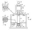
- FIG. 7depicts a wash station in the substrate table according to an embodiment of the invention.
- FIG. 8depicts an ultrasonic cleaning bath according to an embodiment of the invention.
- FIG. 1schematically depicts a lithographic apparatus according to one embodiment of the invention.
- the apparatuscomprises:
- the illumination systemmay include various types of optical components, such as refractive, reflective, magnetic, electromagnetic, electrostatic or other types of optical components, or any combination thereof, for directing, shaping, or controlling radiation.
- optical componentssuch as refractive, reflective, magnetic, electromagnetic, electrostatic or other types of optical components, or any combination thereof, for directing, shaping, or controlling radiation.
- the support structuresupports, i.e. bears the weight of, the patterning device. It holds the patterning device in a manner that depends on the orientation of the patterning device, the design of the lithographic apparatus, and other conditions, such as for example whether or not the patterning device is held in a vacuum environment.
- the support structurecan use mechanical, vacuum, electrostatic or other clamping techniques to hold the patterning device.
- the support structuremay be a frame or a table, for example, which may be fixed or movable as required.
- the support structuremay ensure that the patterning device is at a desired position, for example with respect to the projection system. Any use of the terms “reticle” or “mask” herein may be considered synonymous with the more general term “patterning device.”
- patterning deviceused herein should be broadly interpreted as referring to any device that can be used to impart a radiation beam with a pattern in its cross-section such as to create a pattern in a target portion of the substrate. It should be noted that the pattern imparted to the radiation beam may not exactly correspond to the desired pattern in the target portion of the substrate, for example if the pattern includes phase-shifting features or so called assist features. Generally, the pattern imparted to the radiation beam will correspond to a particular functional layer in a device being created in the target portion, such as an integrated circuit.
- the patterning devicemay be transmissive or reflective.
- Examples of patterning devicesinclude masks, programmable mirror arrays, and programmable LCD panels.
- Masksare well known in lithography, and include mask types such as binary, alternating phase-shift, and attenuated phase-shift, as well as various hybrid mask types.
- An example of a programmable mirror arrayemploys a matrix arrangement of small mirrors, each of which can be individually tilted so as to reflect an incoming radiation beam in different directions. The tilted mirrors impart a pattern in a radiation beam which is reflected by the mirror matrix.
- projection systemused herein should be broadly interpreted as encompassing any type of projection system, including refractive, reflective, catadioptric, magnetic, electromagnetic and electrostatic optical systems, or any combination thereof, as appropriate for the exposure radiation being used, or for other factors such as the use of an immersion liquid or the use of a vacuum. Any use of the term “projection lens” herein may be considered as synonymous with the more general term “projection system”.
- the apparatusis of a transmissive type (e.g. employing a transmissive mask).
- the apparatusmay be of a reflective type (e.g. employing a programmable mirror array of a type as referred to above, or employing a reflective mask).
- the lithographic apparatusmay be of a type having two (dual stage) or more substrate tables (and/or two or more support structures). In such “multiple stage” machines the additional tables may be used in parallel, or preparatory steps may be carried out on one or more tables while one or more other tables are being used for exposure.
- the illuminator ILreceives a radiation beam from a radiation source SO.
- the source and the lithographic apparatusmay be separate entities, for example when the source is an excimer laser. In such cases, the source is not considered to form part of the lithographic apparatus and the radiation beam is passed from the source SO to the illuminator IL with the aid of a beam delivery system BD comprising, for example, suitable directing mirrors and/or a beam expander. In other cases the source may be an integral part of the lithographic apparatus, for example when the source is a mercury lamp.
- the source SO and the illuminator IL, together with the beam delivery system BD if required,may be referred to as a radiation system.
- the illuminator ILmay comprise an adjuster AD for adjusting the angular intensity distribution of the radiation beam.
- an adjuster ADfor adjusting the angular intensity distribution of the radiation beam.
- the illuminator ILmay comprise various other components, such as an integrator IN and a condenser CO.
- the illuminatormay be used to condition the radiation beam, to have a desired uniformity and intensity distribution in its cross-section.
- the radiation beam Bis incident on the patterning device (e.g., mask MA), which is held on the support structure MT (e.g., mask table), and is patterned by the patterning device. Having traversed the patterning device MA, the radiation beam B passes through the projection system PS, which focuses the beam onto a target portion C of the substrate W.
- the substrate table WTcan be moved accurately, e.g. so as to position different target portions C in the path of the radiation beam B.
- the first positioner PM and another position sensor(which is not explicitly depicted in FIG.
- the support structure MTcan be used to accurately position the patterning device MA with respect to the path of the radiation beam B, e.g. after mechanical retrieval from a mask library, or during a scan.
- movement of the support structure MTmay be realized with the aid of a long-stroke module (coarse positioning) and a short-stroke module (fine positioning), which form part of the first positioner PM.
- movement of the substrate table WTmay be realized using a long-stroke module and a short-stroke module, which form part of the second positioner PW.
- the support structure MTmay be connected to a short-stroke actuator only, or may be fixed.
- Patterning device MA and substrate Wmay be aligned using patterning device alignment marks M 1 , M 2 and substrate alignment marks P 1 , P 2 .
- the substrate alignment marks as illustratedoccupy dedicated target portions, they may be located in spaces between target portions (these are known as scribe-lane alignment marks).
- the patterning device alignment marksmay be located between the dies.
- the depicted apparatuscould be used in at least one of the following modes:
- step modethe support structure MT and the substrate table WT are kept essentially stationary, while an entire pattern imparted to the radiation beam is projected onto a target portion C at one time (i.e. a single static exposure).
- the substrate table WTis then shifted in the X and/or Y direction so that a different target portion C can be exposed.
- step modethe maximum size of the exposure field limits the size of the target portion C imaged in a single static exposure.
- the support structure MT and the substrate table WTare scanned synchronously while a pattern imparted to the radiation beam is projected onto a target portion C (i.e. a single dynamic exposure).
- the velocity and direction of the substrate table WT relative to the support structure MTmay be determined by the (de-)magnification and image reversal characteristics of the projection system PS.
- the maximum size of the exposure fieldlimits the width (in the non-scanning direction) of the target portion in a single dynamic exposure, whereas the length of the scanning motion determines the height (in the scanning direction) of the target portion.
- the support structure MTis kept essentially stationary holding a programmable patterning device, and the substrate table WT is moved or scanned while a pattern imparted to the radiation beam is projected onto a target portion C.
- a pulsed radiation sourceis employed and the programmable patterning device is updated as required after each movement of the substrate table WT or in between successive radiation pulses during a scan.
- This mode of operationcan be readily applied to maskless lithography that utilizes programmable patterning device, such as a programmable mirror array of a type as referred to above.
- FIG. 4A further immersion lithography solution with a localized liquid supply system is shown in FIG. 4 .
- Liquidis supplied by two groove inlets IN on either side of the projection system PL and is removed by a plurality of discrete outlets OUT arranged radially outwardly of the inlets IN.
- the inlets IN and OUTcan be arranged in a plate with a hole in its center and through which the projection beam is projected.
- Liquidis supplied by one groove inlet IN on one side of the projection system PL and removed by a plurality of discrete outlets OUT on the other side of the projection system PL, causing a flow of a thin film of liquid between the projection system PL and the substrate W.
- the choice of which combination of inlet IN and outlets OUT to usecan depend on the direction of movement of the substrate W (the other combination of inlet IN and outlets OUT being inactive).
- Another immersion lithography solution with a localized liquid supply system solutionwhich has been proposed is to provide the liquid supply system with a liquid confinement structure which extends along at least a part of a boundary of the space between the final element of the projection system and the substrate table.
- the liquid confinement structureis substantially stationary relative to the projection system in the XY plane though there may be some relative movement in the Z direction (in the direction of the optical axis).
- a sealis formed between the liquid confinement structure and the surface of the substrate.
- the sealis a contactless seal such as a gas seal.
- FIG. 5shows a liquid supply system comprising a liquid confinement structure (sometimes referred to as an immersion hood or showerhead) according to an embodiment of the invention.
- a liquid confinement structuresometimes referred to as an immersion hood or showerhead
- FIG. 5depicts an arrangement of a reservoir 10 , which forms a contactless seal to the substrate around the image field of the projection system so that liquid is confined to fill a space between the substrate surface and the final element of the projection system.
- a liquid confinement structure 12 positioned below and surrounding the final element of the projection system PLforms the reservoir. Liquid is brought into the space below the projection system and within the liquid confinement structure 12 .
- the liquid confinement structure 12extends a little above the final element of the projection system and the liquid level rises above the final element so that a buffer of liquid is provided.
- the liquid confinement structure 12has an inner periphery that at the upper end preferably closely conforms to the shape of the projection system or the final element thereof and may, e.g., be round. At the bottom, the inner periphery closely conforms to the shape of the image field, e.g., rectangular though this need not be the case.
- the liquidis confined in the reservoir by a gas seal 16 between the bottom of the liquid confinement structure 12 and the surface of the substrate W.
- the gas sealis formed by gas, e.g. air, synthetic air, N 2 or an inert gas, provided under pressure via inlet 15 to the gap between liquid confinement structure 12 and substrate and extracted via outlet 14 .
- gase.g. air, synthetic air, N 2 or an inert gas
- the overpressure on the gas inlet 15 , vacuum level on the outlet 14 and geometry of the gapare arranged so that there is a high-velocity gas flow inwards that confines the liquid.
- other types of sealcould be used to contain the liquid such as simply an outlet to remove liquid and/or gas.
- the liquid confinement structure 12 and the projection system PLare positioned in such a way over the substrate W that the substrate may be exposed, the patterned beam of radiation passing through the liquid 11 from the projection system PL to the substrate W.
- the liquid confinement structure 12 and the substrate table WThave moved relative to each other so that the aperture holding liquid of the liquid confinement structure 12 is no longer completely over the substrate W. While the liquid confinement structure aperture extends beyond the surface of the substrate W, for example, the immersion liquid 11 can be replaced with a cleaning fluid 110 which may be supplied to the liquid confinement structure via the same outlet 13 as the immersion liquid 11 . In this case, the cleaning device is the liquid confinement structure.
- the cleaning fluid 110may be used to remove contaminants from both the final element of the projection system PL and/or the substrate table WT. Furthermore, the pressurized gas flow via outlet 14 and inlet 15 may also be used to clean the substrate table. Contaminants are washed away or broken down and removed when the cleaning fluid 110 is removed and replaced by immersion liquid 11 , ready to expose the next substrate.
- the cleaning fluid 110which may be supplied by the liquid confinement structure, itself may be a solvent, a detergent, a liquefied gas such as carbon dioxide, or a dissolved gas such as oxygen, ozone or nitrogen.
- the liquid confinement structuremay be used to contain cleaning gases as well as liquids.
- the gap between the projection system PL and the liquid confinement structure 12may be temporarily closed during the cleaning action and even gases that are potentially harmful to humans or to other parts of the lithographic apparatus may be used.
- the cleaning action using the liquid confinement structuremay be part of an exposure, or it may be part of a maintenance action when, for example, contamination levels require it.
- Softwaremay be used to guide movement of the substrate table further in every direction or desired direction than is required for mere exposure of the substrate. In this way, the entirety or a desired part of the substrate table WT may be cleaned because the entire or desired surface may, at some point, be beneath the liquid confinement structure.
- FIG. 7Another cleaning device configured to supply cleaning fluid to the liquid confinement structure is, referring to FIG. 7 , a cleaning station 20 provided in the substrate table WT.
- the cleaning station 20When cleaning of the final element of the projection system PL and/or of the substrate table WT is required, the cleaning station 20 is moved relative to the liquid confinement structure so that the cleaning station is below the final element.
- cleaning liquid 110is provided from the cleaning station 20 by a sprayer configured to sprayed the cleaning liquid 110 into the reservoir of the liquid confinement structure 12 and onto the final element of the projection system PL.
- the cleaning liquid 110can thereby clean the final element. Additionally or alternatively, the cleaning liquid 110 may fill up the reservoir so that the substrate table WT may be cleaned.
- the liquid confinement structure 12may then be activated so that ultra pure water or any other appropriate liquid rinses away any remaining cleaning liquid.
- the cleaning stationmay provide a cleaning gas such as ozone or a plasma.
- the cleaning liquidmay be liquid CO 2 (this cleaning may be known as “snow cleaning”).
- the cleaning fluid usedwill depend on the contaminant to be removed. Drying stains are usually salt deposits and depending on the exact salt, high or low pH solutions may be used. Other detergents may be used to remove metal deposits. For organic contaminants, organic solvents such as heptane, hexane (which are non polar), alcohol, e.g. ethanol, or acetone (which are polar) may be used.
- a projection beammay be projected through the final element PL during cleaning to break down certain organic contaminants.
- the liquid confinement structure 12 and/or the substrate table WTmay contain a brush on a motor.
- the cleaning station 20may be positioned anywhere in or on the substrate table WT or in or on the liquid confinement structure 12 so that the liquid confinement structure itself, a closing plate and so on may also be cleaned. Many surfaces in an immersion lithographic apparatus are at risk of contamination because of drying stains, organics contaminants from the resist evaporating off the substrate, contaminations from the immersion liquid itself, and so on. Accordingly, the cleaning fluid 110 , whether provided by the liquid confinement structure 12 or by the cleaning station 20 , may be provided to all the same surfaces that may be exposed to immersion liquid.
- FIG. 8shows another embodiment in which the immersion system, and in particular the final element of the projection system PL, may be cleaned.
- the liquid in the liquid confinement structure 12may be transformed into an ultrasonic cleaning bath by the incorporation of an ultrasonic emitter 30 in the substrate table WT and/or in the liquid confinement structure 12 as a cleaning device.
- Ultrasonic cleaningis particularly good for removing contaminants that have dried and hardened, for example, salts on the final element of the projection system PL. Ultrasonic cleaning is also useful for cleaning in areas that brushes or tissues cannot reach, such as the pimples in a pimple or burl-plate of the substrate table WT.
- a coatingmay be introduced into the reservoir of the liquid confinement structure 12 via the liquid confinement structure 12 and/or via the cleaning station 20 .
- the liquid confinement structure and/or the cleaning stationmay be referred to as a coater.
- the coatingmay be used to protect the liquid confinement structure, the final element, or other surfaces, or may be for other uses which would be clear to the person skilled in the art.
- a coating removal agentmay be introduced into the liquid confinement structure in the same way.
- UV radiationAnother cleaning device that may be used for cleaning microbiological contamination (i.e., bacterial cultures) is UV radiation.
- the radiation source of the lithographic apparatusmay be used to supply this UV radiation, although another source could be used.
- the radiation source of a lithographic apparatusmay emit 193 nm radiation, a type of radiation which kills bacteria that may be present in the liquid confinement structure, on the substrate table, and/or on the final element.
- a first wayis with a closing plate that is transparent to the UV radiation so that the closing plate holds the liquid within the liquid confinement structure 12 but the UV radiation may nonetheless reach the substrate table WT and kill the bacteria on it.
- a second wayis not to use a closing disc, but to irradiate bacteria and simultaneously to wash the dead bacteria away with the flow of the liquid in the liquid confinement structure 12 .
- the UV radiationmay be provided by the projection system PL itself as described above, or it may be provided by a separate optical element.
- an optical element positioned in the same place as the ultrasound emitter 30 in FIG. 8may be used to supply the UV radiation to the final element of the projection system PL and/or a surface of the liquid confinement structure 12 .
- the UV radiationmay in that case, for example, enter the liquid confinement structure 12 via a closing plate that is transparent to the UV radiation.
- UV radiationhas an advantage of keeping microbiological contamination low while preventing prolonged downtime, which can be caused by having to perform wet chemical sanitizing using hydrogen peroxide or ozonated water, for instance.
- This treatmentcan be carried out as a preventative or curative measure.
- lithographic apparatusin the manufacture of ICs
- the lithographic apparatus described hereinmay have other applications, such as the manufacture of integrated optical systems, guidance and detection patterns for magnetic domain memories, flat-panel displays, liquid-crystal displays (LCDs), thin-film magnetic heads, etc.
- LCDsliquid-crystal displays
- any use of the terms “wafer” or “die” hereinmay be considered as synonymous with the more general terms “substrate” or “target portion”, respectively.
- the substrate referred to hereinmay be processed, before or after exposure, in for example a track (a tool that typically applies a layer of resist to a substrate and develops the exposed resist), a metrology tool and/or an inspection tool. Where applicable, the disclosure herein may be applied to such and other substrate processing tools. Further, the substrate may be processed more than once, for example in order to create a multi-layer IC, so that the term substrate used herein may also refer to a substrate that already contains multiple processed layers.
- UV radiatione.g. having a wavelength of or about 365, 248, 193, 157 or 126 nm.
- lensmay refer to any one or combination of various types of optical components, including refractive and reflective optical components.
- the inventionmay take the form of a computer program containing one or more sequences of machine-readable instructions describing a method as disclosed above, or a data storage medium (e.g. semiconductor memory, magnetic or optical disk) having such a computer program stored therein.
- a data storage mediume.g. semiconductor memory, magnetic or optical disk
- a liquid supply systemis any mechanism that provides a liquid to a space between the projection system and the substrate and/or substrate table. It may comprise any combination of one or more structures, one or more liquid inlets, one or more gas inlets, one or more gas outlets, and/or one or more liquid outlets, the combination providing and confining the liquid to the space.
- a surface of the spacemay be limited to a portion of the substrate and/or substrate table, a surface of the space may completely cover a surface of the substrate and/or substrate table, or the space may envelop the substrate and/or substrate table.
Landscapes
- Physics & Mathematics (AREA)
- General Physics & Mathematics (AREA)
- Engineering & Computer Science (AREA)
- Public Health (AREA)
- Health & Medical Sciences (AREA)
- Epidemiology (AREA)
- Atmospheric Sciences (AREA)
- Life Sciences & Earth Sciences (AREA)
- Plasma & Fusion (AREA)
- Environmental & Geological Engineering (AREA)
- Exposure And Positioning Against Photoresist Photosensitive Materials (AREA)
- Exposure Of Semiconductors, Excluding Electron Or Ion Beam Exposure (AREA)
- Container, Conveyance, Adherence, Positioning, Of Wafer (AREA)
Abstract
Description
- an illumination system (illuminator) IL configured to condition a radiation beam B (e.g. UV radiation or DUV radiation).
- a support structure (e.g. a mask table) MT constructed to support a patterning device (e.g. a mask) MA and connected to a first positioner PM configured to accurately position the patterning device in accordance with certain parameters;
- a substrate table (e.g. a wafer table) WT constructed to hold a substrate (e.g. a resist-coated wafer) W and connected to a second positioner PW configured to accurately position the substrate in accordance with certain parameters; and
- a projection system (e.g. a refractive projection lens system) PS configured to project a pattern imparted to the radiation beam B by patterning device MA onto a target portion C (e.g. comprising one or more dies) of the substrate W.
Claims (31)
Priority Applications (5)
| Application Number | Priority Date | Filing Date | Title |
|---|---|---|---|
| US11/656,560US8115899B2 (en) | 2004-12-20 | 2007-01-23 | Lithographic apparatus and device manufacturing method |
| US12/986,576US8638419B2 (en) | 2004-12-20 | 2011-01-07 | Lithographic apparatus and device manufacturing method |
| US13/242,401US8941811B2 (en) | 2004-12-20 | 2011-09-23 | Lithographic apparatus and device manufacturing method |
| US14/584,826US9703210B2 (en) | 2004-12-20 | 2014-12-29 | Lithographic apparatus and device manufacturing method |
| US15/624,419US10509326B2 (en) | 2004-12-20 | 2017-06-15 | Lithographic apparatus and device manufacturing method |
Applications Claiming Priority (2)
| Application Number | Priority Date | Filing Date | Title |
|---|---|---|---|
| US11/015,767US7880860B2 (en) | 2004-12-20 | 2004-12-20 | Lithographic apparatus and device manufacturing method |
| US11/656,560US8115899B2 (en) | 2004-12-20 | 2007-01-23 | Lithographic apparatus and device manufacturing method |
Related Parent Applications (1)
| Application Number | Title | Priority Date | Filing Date |
|---|---|---|---|
| US11/015,767ContinuationUS7880860B2 (en) | 2004-12-20 | 2004-12-20 | Lithographic apparatus and device manufacturing method |
Related Child Applications (1)
| Application Number | Title | Priority Date | Filing Date |
|---|---|---|---|
| US12/986,576ContinuationUS8638419B2 (en) | 2004-12-20 | 2011-01-07 | Lithographic apparatus and device manufacturing method |
Publications (2)
| Publication Number | Publication Date |
|---|---|
| US20080002162A1 US20080002162A1 (en) | 2008-01-03 |
| US8115899B2true US8115899B2 (en) | 2012-02-14 |
Family
ID=36595231
Family Applications (6)
| Application Number | Title | Priority Date | Filing Date |
|---|---|---|---|
| US11/015,767Expired - Fee RelatedUS7880860B2 (en) | 2004-12-20 | 2004-12-20 | Lithographic apparatus and device manufacturing method |
| US11/656,560Expired - Fee RelatedUS8115899B2 (en) | 2004-12-20 | 2007-01-23 | Lithographic apparatus and device manufacturing method |
| US12/986,576Expired - Fee RelatedUS8638419B2 (en) | 2004-12-20 | 2011-01-07 | Lithographic apparatus and device manufacturing method |
| US13/242,401Expired - Fee RelatedUS8941811B2 (en) | 2004-12-20 | 2011-09-23 | Lithographic apparatus and device manufacturing method |
| US14/584,826Expired - Fee RelatedUS9703210B2 (en) | 2004-12-20 | 2014-12-29 | Lithographic apparatus and device manufacturing method |
| US15/624,419Expired - LifetimeUS10509326B2 (en) | 2004-12-20 | 2017-06-15 | Lithographic apparatus and device manufacturing method |
Family Applications Before (1)
| Application Number | Title | Priority Date | Filing Date |
|---|---|---|---|
| US11/015,767Expired - Fee RelatedUS7880860B2 (en) | 2004-12-20 | 2004-12-20 | Lithographic apparatus and device manufacturing method |
Family Applications After (4)
| Application Number | Title | Priority Date | Filing Date |
|---|---|---|---|
| US12/986,576Expired - Fee RelatedUS8638419B2 (en) | 2004-12-20 | 2011-01-07 | Lithographic apparatus and device manufacturing method |
| US13/242,401Expired - Fee RelatedUS8941811B2 (en) | 2004-12-20 | 2011-09-23 | Lithographic apparatus and device manufacturing method |
| US14/584,826Expired - Fee RelatedUS9703210B2 (en) | 2004-12-20 | 2014-12-29 | Lithographic apparatus and device manufacturing method |
| US15/624,419Expired - LifetimeUS10509326B2 (en) | 2004-12-20 | 2017-06-15 | Lithographic apparatus and device manufacturing method |
Country Status (2)
| Country | Link |
|---|---|
| US (6) | US7880860B2 (en) |
| JP (6) | JP4825510B2 (en) |
Cited By (2)
| Publication number | Priority date | Publication date | Assignee | Title |
|---|---|---|---|---|
| US9919939B2 (en) | 2011-12-06 | 2018-03-20 | Delta Faucet Company | Ozone distribution in a faucet |
| US11458214B2 (en) | 2015-12-21 | 2022-10-04 | Delta Faucet Company | Fluid delivery system including a disinfectant device |
Families Citing this family (76)
| Publication number | Priority date | Publication date | Assignee | Title |
|---|---|---|---|---|
| CN101825847B (en)* | 2003-04-11 | 2013-10-16 | 株式会社尼康 | Cleanup method for optics in immersion lithography |
| TW201806001A (en) | 2003-05-23 | 2018-02-16 | 尼康股份有限公司 | Exposure device and device manufacturing method |
| EP2261741A3 (en)* | 2003-06-11 | 2011-05-25 | ASML Netherlands B.V. | Lithographic apparatus and device manufacturing method |
| TWI245163B (en) | 2003-08-29 | 2005-12-11 | Asml Netherlands Bv | Lithographic apparatus and device manufacturing method |
| US7050146B2 (en) | 2004-02-09 | 2006-05-23 | Asml Netherlands B.V. | Lithographic apparatus and device manufacturing method |
| EP3203498A1 (en) | 2004-06-09 | 2017-08-09 | Nikon Corporation | Exposure apparatus and device manufacturing method |
| WO2005124833A1 (en)* | 2004-06-21 | 2005-12-29 | Nikon Corporation | Exposure device, exposure device member cleaning method, exposure device maintenance method, maintenance device, and device manufacturing method |
| US8698998B2 (en)* | 2004-06-21 | 2014-04-15 | Nikon Corporation | Exposure apparatus, method for cleaning member thereof, maintenance method for exposure apparatus, maintenance device, and method for producing device |
| JP2006024692A (en)* | 2004-07-07 | 2006-01-26 | Toshiba Corp | Resist pattern forming method |
| US7224427B2 (en)* | 2004-08-03 | 2007-05-29 | Taiwan Semiconductor Manufacturing Company, Ltd. | Megasonic immersion lithography exposure apparatus and method |
| JP4772306B2 (en)* | 2004-09-06 | 2011-09-14 | 株式会社東芝 | Immersion optical device and cleaning method |
| US7385670B2 (en)* | 2004-10-05 | 2008-06-10 | Asml Netherlands B.V. | Lithographic apparatus, cleaning system and cleaning method for in situ removing contamination from a component in a lithographic apparatus |
| CN101044594B (en)* | 2004-10-26 | 2010-05-12 | 株式会社尼康 | Substrate processing method, exposure apparatus, and device manufacturing method |
| US20070242248A1 (en)* | 2004-10-26 | 2007-10-18 | Nikon Corporation | Substrate processing method, exposure apparatus, and method for producing device |
| JP4784513B2 (en)* | 2004-12-06 | 2011-10-05 | 株式会社ニコン | Maintenance method, maintenance equipment, exposure apparatus, and device manufacturing method |
| US7880860B2 (en)* | 2004-12-20 | 2011-02-01 | Asml Netherlands B.V. | Lithographic apparatus and device manufacturing method |
| US7450217B2 (en)* | 2005-01-12 | 2008-11-11 | Asml Netherlands B.V. | Exposure apparatus, coatings for exposure apparatus, lithographic apparatus, device manufacturing method, and device manufactured thereby |
| JP2006261606A (en)* | 2005-03-18 | 2006-09-28 | Canon Inc | Exposure apparatus, exposure method, and device manufacturing method |
| US7291850B2 (en)* | 2005-04-08 | 2007-11-06 | Asml Netherlands B.V. | Lithographic apparatus and device manufacturing method |
| US7315033B1 (en)* | 2005-05-04 | 2008-01-01 | Advanced Micro Devices, Inc. | Method and apparatus for reducing biological contamination in an immersion lithography system |
| KR100638107B1 (en)* | 2005-06-09 | 2006-10-24 | 연세대학교 산학협력단 | Optical modulation micro-opening array device having immersion thin film layer and high speed micro pattern recording system using same |
| JP2007012375A (en)* | 2005-06-29 | 2007-01-18 | Toyota Motor Corp | FUEL CELL, FUEL CELL ELECTRODE CATALYST MANUFACTURING METHOD, AND FUEL CELL OPERATING METHOD |
| US7291569B2 (en)* | 2005-06-29 | 2007-11-06 | Infineon Technologies Ag | Fluids for immersion lithography systems |
| US20070004182A1 (en)* | 2005-06-30 | 2007-01-04 | Taiwan Semiconductor Manufacturing Company, Ltd. | Methods and system for inhibiting immersion lithography defect formation |
| KR20080031376A (en)* | 2005-07-11 | 2008-04-08 | 가부시키가이샤 니콘 | Exposure apparatus and device manufacturing method |
| US7986395B2 (en)* | 2005-10-24 | 2011-07-26 | Taiwan Semiconductor Manufacturing Company, Ltd. | Immersion lithography apparatus and methods |
| JP2007150102A (en)* | 2005-11-29 | 2007-06-14 | Fujitsu Ltd | Exposure apparatus and optical element cleaning method |
| US8125610B2 (en)* | 2005-12-02 | 2012-02-28 | ASML Metherlands B.V. | Method for preventing or reducing contamination of an immersion type projection apparatus and an immersion type lithographic apparatus |
| JP2007266074A (en)* | 2006-03-27 | 2007-10-11 | Toshiba Corp | Semiconductor device manufacturing method and immersion lithography system |
| TW200805000A (en)* | 2006-05-18 | 2008-01-16 | Nikon Corp | Exposure method and apparatus, maintenance method and device manufacturing method |
| CN102109773A (en)* | 2006-05-22 | 2011-06-29 | 株式会社尼康 | Exposure method, exposure apparatus, and maintenance method |
| US7969548B2 (en)* | 2006-05-22 | 2011-06-28 | Asml Netherlands B.V. | Lithographic apparatus and lithographic apparatus cleaning method |
| EP2034515A4 (en)* | 2006-05-23 | 2012-01-18 | Nikon Corp | Maintenance method, exposure method and apparatus, and device manufacturing method |
| US8564759B2 (en)* | 2006-06-29 | 2013-10-22 | Taiwan Semiconductor Manufacturing Company, Ltd. | Apparatus and method for immersion lithography |
| EP2043134A4 (en)* | 2006-06-30 | 2012-01-25 | Nikon Corp | Maintenance method, exposure method and apparatus and device manufacturing method |
| KR101523388B1 (en)* | 2006-08-30 | 2015-05-27 | 가부시키가이샤 니콘 | Exposure apparatus, device manufacturing method, cleaning method and member for cleaning |
| WO2008029884A1 (en)* | 2006-09-08 | 2008-03-13 | Nikon Corporation | Cleaning member, cleaning method and device manufacturing method |
| US8040490B2 (en)* | 2006-12-01 | 2011-10-18 | Nikon Corporation | Liquid immersion exposure apparatus, exposure method, and method for producing device |
| US8013975B2 (en)* | 2006-12-01 | 2011-09-06 | Nikon Corporation | Exposure apparatus, exposure method, and method for producing device |
| US20080156356A1 (en) | 2006-12-05 | 2008-07-03 | Nikon Corporation | Cleaning liquid, cleaning method, liquid generating apparatus, exposure apparatus, and device fabricating method |
| WO2008089990A2 (en)* | 2007-01-26 | 2008-07-31 | Carl Zeiss Smt Ag | Method for operating an immersion lithography apparatus |
| US8817226B2 (en) | 2007-02-15 | 2014-08-26 | Asml Holding N.V. | Systems and methods for insitu lens cleaning using ozone in immersion lithography |
| US8654305B2 (en)* | 2007-02-15 | 2014-02-18 | Asml Holding N.V. | Systems and methods for insitu lens cleaning in immersion lithography |
| JP4366407B2 (en)* | 2007-02-16 | 2009-11-18 | キヤノン株式会社 | Exposure apparatus and device manufacturing method |
| US8011377B2 (en) | 2007-05-04 | 2011-09-06 | Asml Netherlands B.V. | Cleaning device and a lithographic apparatus cleaning method |
| US7866330B2 (en) | 2007-05-04 | 2011-01-11 | Asml Netherlands B.V. | Cleaning device, a lithographic apparatus and a lithographic apparatus cleaning method |
| US7841352B2 (en)* | 2007-05-04 | 2010-11-30 | Asml Netherlands B.V. | Cleaning device, a lithographic apparatus and a lithographic apparatus cleaning method |
| US8947629B2 (en)* | 2007-05-04 | 2015-02-03 | Asml Netherlands B.V. | Cleaning device, a lithographic apparatus and a lithographic apparatus cleaning method |
| JP2009033111A (en)* | 2007-05-28 | 2009-02-12 | Nikon Corp | Exposure apparatus, device manufacturing method, cleaning apparatus, cleaning method, and exposure method |
| US7916269B2 (en)* | 2007-07-24 | 2011-03-29 | Asml Netherlands B.V. | Lithographic apparatus and contamination removal or prevention method |
| US20090025753A1 (en)* | 2007-07-24 | 2009-01-29 | Asml Netherlands B.V. | Lithographic Apparatus And Contamination Removal Or Prevention Method |
| NL1035942A1 (en)* | 2007-09-27 | 2009-03-30 | Asml Netherlands Bv | Lithographic Apparatus and Method of Cleaning a Lithographic Apparatus. |
| SG151198A1 (en)* | 2007-09-27 | 2009-04-30 | Asml Netherlands Bv | Methods relating to immersion lithography and an immersion lithographic apparatus |
| JP5017232B2 (en)* | 2007-10-31 | 2012-09-05 | エーエスエムエル ネザーランズ ビー.ブイ. | Cleaning apparatus and immersion lithography apparatus |
| SG183058A1 (en)* | 2007-12-17 | 2012-08-30 | Nikon Corp | Exposure apparatus, exposure method and device manufacturing method |
| NL1036273A1 (en)* | 2007-12-18 | 2009-06-19 | Asml Netherlands Bv | Lithographic apparatus and method of cleaning a surface or an immersion lithographic apparatus. |
| NL1036306A1 (en) | 2007-12-20 | 2009-06-23 | Asml Netherlands Bv | Lithographic apparatus and in-line cleaning apparatus. |
| US8451425B2 (en)* | 2007-12-28 | 2013-05-28 | Nikon Corporation | Exposure apparatus, exposure method, cleaning apparatus, and device manufacturing method |
| US8339572B2 (en) | 2008-01-25 | 2012-12-25 | Asml Netherlands B.V. | Lithographic apparatus and device manufacturing method |
| US20100039628A1 (en)* | 2008-03-19 | 2010-02-18 | Nikon Corporation | Cleaning tool, cleaning method, and device fabricating method |
| NL1036709A1 (en) | 2008-04-24 | 2009-10-27 | Asml Netherlands Bv | Lithographic apparatus and a method of operating the apparatus. |
| US7838425B2 (en)* | 2008-06-16 | 2010-11-23 | Kabushiki Kaisha Toshiba | Method of treating surface of semiconductor substrate |
| JP2010021370A (en)* | 2008-07-10 | 2010-01-28 | Canon Inc | Immersion exposure equipment and method of manufacturing device |
| US20100045949A1 (en)* | 2008-08-11 | 2010-02-25 | Nikon Corporation | Exposure apparatus, maintaining method and device fabricating method |
| EP2159638B1 (en)* | 2008-08-26 | 2015-06-17 | ASML Netherlands BV | Radiation source and lithographic apparatus |
| NL2003363A (en)* | 2008-09-10 | 2010-03-15 | Asml Netherlands Bv | Lithographic apparatus, method of manufacturing an article for a lithographic apparatus and device manufacturing method. |
| JP5120193B2 (en)* | 2008-10-08 | 2013-01-16 | 株式会社ニコン | Exposure apparatus, maintenance method, exposure method, and device manufacturing method |
| JPWO2010050240A1 (en)* | 2008-10-31 | 2012-03-29 | 株式会社ニコン | Exposure apparatus, exposure method, and device manufacturing method |
| EP2455934B1 (en) | 2009-07-17 | 2018-05-23 | Mitsubishi Electric Corporation | Facility operation display device, air-conditioning system, and program |
| NL2005610A (en) | 2009-12-02 | 2011-06-06 | Asml Netherlands Bv | Lithographic apparatus and surface cleaning method. |
| JP5404361B2 (en) | 2009-12-11 | 2014-01-29 | 株式会社東芝 | Semiconductor substrate surface treatment apparatus and method |
| MX2012007581A (en)* | 2009-12-28 | 2012-07-30 | Pioneer Hi Bred Int | Sorghum fertility restorer genotypes and methods of marker-assisted selection. |
| NL2006127A (en)* | 2010-02-17 | 2011-08-18 | Asml Netherlands Bv | A substrate table, a lithographic apparatus and a method for manufacturing a device using a lithographic apparatus. |
| US20120019803A1 (en)* | 2010-07-23 | 2012-01-26 | Nikon Corporation | Cleaning method, liquid immersion member, immersion exposure apparatus, device fabricating method, program, and storage medium |
| US20120019802A1 (en)* | 2010-07-23 | 2012-01-26 | Nikon Corporation | Cleaning method, immersion exposure apparatus, device fabricating method, program, and storage medium |
| US20180032409A1 (en) | 2016-07-26 | 2018-02-01 | Netapp, Inc. | Backup and recovery of application data of an application executing in a virtual machine |
Citations (208)
| Publication number | Priority date | Publication date | Assignee | Title |
|---|---|---|---|---|
| US3573975A (en) | 1968-07-10 | 1971-04-06 | Ibm | Photochemical fabrication process |
| US3648587A (en) | 1967-10-20 | 1972-03-14 | Eastman Kodak Co | Focus control for optical instruments |
| EP0023231B1 (en) | 1979-07-27 | 1982-08-11 | Tabarelli, Werner, Dr. | Optical lithographic method and apparatus for copying a pattern onto a semiconductor wafer |
| US4346164A (en) | 1980-10-06 | 1982-08-24 | Werner Tabarelli | Photolithographic method for the manufacture of integrated circuits |
| US4390273A (en) | 1981-02-17 | 1983-06-28 | Censor Patent-Und Versuchsanstalt | Projection mask as well as a method and apparatus for the embedding thereof and projection printing system |
| US4396705A (en) | 1980-09-19 | 1983-08-02 | Hitachi, Ltd. | Pattern forming method and pattern forming apparatus using exposures in a liquid |
| US4468120A (en) | 1981-02-04 | 1984-08-28 | Nippon Kogaku K.K. | Foreign substance inspecting apparatus |
| US4480910A (en) | 1981-03-18 | 1984-11-06 | Hitachi, Ltd. | Pattern forming apparatus |
| US4509852A (en) | 1980-10-06 | 1985-04-09 | Werner Tabarelli | Apparatus for the photolithographic manufacture of integrated circuit elements |
| FR2474708B1 (en) | 1980-01-24 | 1987-02-20 | Dme | HIGH-RESOLUTION MICROPHOTOLITHOGRAPHY PROCESS |
| US5040020A (en) | 1988-03-31 | 1991-08-13 | Cornell Research Foundation, Inc. | Self-aligned, high resolution resonant dielectric lithography |
| EP0418427A3 (en) | 1989-09-06 | 1992-01-22 | Eiichi Miyake | Exposure process |
| US5121256A (en) | 1991-03-14 | 1992-06-09 | The Board Of Trustees Of The Leland Stanford Junior University | Lithography system employing a solid immersion lens |
| US5257128A (en) | 1988-06-22 | 1993-10-26 | Board Of Regents, The University Of Texas System | Freezing/perfusion microscope stage |
| US5587794A (en) | 1990-12-13 | 1996-12-24 | Nikon Corporation | Surface position detection apparatus |
| US5610683A (en) | 1992-11-27 | 1997-03-11 | Canon Kabushiki Kaisha | Immersion type projection exposure apparatus |
| US5715039A (en) | 1995-05-19 | 1998-02-03 | Hitachi, Ltd. | Projection exposure apparatus and method which uses multiple diffraction gratings in order to produce a solid state device with fine patterns |
| EP0834773A2 (en) | 1996-10-07 | 1998-04-08 | Nikon Corporation | Focusing and tilting adjustment system for lithography aligner, manufacturing apparatus or inspection apparatus |
| US5900354A (en) | 1997-07-03 | 1999-05-04 | Batchelder; John Samuel | Method for optical inspection and lithography |
| US6236634B1 (en) | 1996-08-26 | 2001-05-22 | Digital Papyrus Corporation | Method and apparatus for coupling an optical lens to a disk through a coupling medium having a relatively high index of refraction |
| US6301055B1 (en) | 2000-08-16 | 2001-10-09 | California Institute Of Technology | Solid immersion lens structures and methods for producing solid immersion lens structures |
| US20020020821A1 (en) | 2000-08-08 | 2002-02-21 | Koninklijke Philips Electronics N.V. | Method of manufacturing an optically scannable information carrier |
| US6459472B1 (en) | 1998-05-15 | 2002-10-01 | Asml Netherlands B.V. | Lithographic device |
| US6466365B1 (en) | 2000-04-07 | 2002-10-15 | Corning Incorporated | Film coated optical lithography elements and method of making |
| US20020163629A1 (en) | 2001-05-07 | 2002-11-07 | Michael Switkes | Methods and apparatus employing an index matching medium |
| US6496257B1 (en)* | 1997-11-21 | 2002-12-17 | Nikon Corporation | Projection exposure apparatus and method |
| US20030030916A1 (en) | 2000-12-11 | 2003-02-13 | Nikon Corporation | Projection optical system and exposure apparatus having the projection optical system |
| US6560032B2 (en) | 2000-03-27 | 2003-05-06 | Olympus Optical Co., Ltd. | Liquid immersion lens system and optical apparatus using the same |
| US20030123040A1 (en) | 2001-11-07 | 2003-07-03 | Gilad Almogy | Optical spot grid array printer |
| US6600547B2 (en) | 2001-09-24 | 2003-07-29 | Nikon Corporation | Sliding seal |
| US6603130B1 (en) | 1999-04-19 | 2003-08-05 | Asml Netherlands B.V. | Gas bearings for use with vacuum chambers and their application in lithographic projection apparatuses |
| US20030157538A1 (en) | 1997-06-18 | 2003-08-21 | Krull Ulrich J. | Nucleic acid biosensor diagnostics |
| US20030174408A1 (en) | 2002-03-08 | 2003-09-18 | Carl Zeiss Smt Ag | Refractive projection objective for immersion lithography |
| US20040000627A1 (en) | 2002-06-28 | 2004-01-01 | Carl Zeiss Semiconductor Manufacturing Technologies Ag | Method for focus detection and an imaging system with a focus-detection system |
| WO2004007417A1 (en)* | 2002-07-12 | 2004-01-22 | The Australian National University | Enzyme inhibitors |
| US20040075895A1 (en) | 2002-10-22 | 2004-04-22 | Taiwan Semiconductor Manufacturing Co., Ltd. | Apparatus for method for immersion lithography |
| US20040109237A1 (en) | 2002-12-09 | 2004-06-10 | Carl Zeiss Smt Ag | Projection objective, especially for microlithography, and method for adjusting a projection objective |
| US20040114117A1 (en) | 2002-11-18 | 2004-06-17 | Asml Netherlands B.V. | Lithographic apparatus and device manufacturing method |
| WO2004053953A1 (en) | 2002-12-10 | 2004-06-24 | Nikon Corporation | Exposure apparatus and method for manufacturing device |
| WO2004053958A1 (en) | 2002-12-10 | 2004-06-24 | Nikon Corporation | Exposure apparatus and method for manufacturing device |
| WO2004053956A1 (en) | 2002-12-10 | 2004-06-24 | Nikon Corporation | Exposure apparatus, exposure method and method for manufacturing device |
| WO2004053955A1 (en) | 2002-12-10 | 2004-06-24 | Nikon Corporation | Exposure system and device producing method |
| WO2004053950A1 (en) | 2002-12-10 | 2004-06-24 | Nikon Corporation | Exposure apparatus and method for manufacturing device |
| US20040119954A1 (en) | 2002-12-10 | 2004-06-24 | Miyoko Kawashima | Exposure apparatus and method |
| WO2004053959A1 (en) | 2002-12-10 | 2004-06-24 | Nikon Corporation | Optical device and projection exposure apparatus using such optical device |
| WO2004053951A1 (en) | 2002-12-10 | 2004-06-24 | Nikon Corporation | Exposure method, exposure apparatus and method for manufacturing device |
| US20040118184A1 (en) | 2002-12-19 | 2004-06-24 | Asml Holding N.V. | Liquid flow proximity sensor for use in immersion lithography |
| WO2004053596A2 (en) | 2002-12-10 | 2004-06-24 | Carl Zeiss Smt Ag | Method for adjusting a desired optical property of a positioning lens and microlithographic projection exposure system |
| WO2004053957A1 (en) | 2002-12-10 | 2004-06-24 | Nikon Corporation | Surface position detection apparatus, exposure method, and device porducing method |
| WO2004053952A1 (en) | 2002-12-10 | 2004-06-24 | Nikon Corporation | Exposure apparatus and method for manufacturing device |
| WO2004053954A1 (en) | 2002-12-10 | 2004-06-24 | Nikon Corporation | Exposure apparatus and method for manufacturing device |
| US20040125351A1 (en) | 2002-12-30 | 2004-07-01 | Krautschik Christof Gabriel | Immersion lithography |
| WO2004055803A1 (en) | 2002-12-13 | 2004-07-01 | Koninklijke Philips Electronics N.V. | Liquid removal in a method and device for irradiating spots on a layer |
| WO2004057589A1 (en) | 2002-12-19 | 2004-07-08 | Koninklijke Philips Electronics N.V. | Method and device for irradiating spots on a layer |
| WO2004057590A1 (en) | 2002-12-19 | 2004-07-08 | Koninklijke Philips Electronics N.V. | Method and device for irradiating spots on a layer |
| US20040136494A1 (en) | 2002-11-12 | 2004-07-15 | Asml Netherlands B.V. | Lithographic apparatus and device manufacturing method |
| US20040135099A1 (en) | 2002-11-29 | 2004-07-15 | Asml Netherlands B.V. | Lithographic apparatus and device manufacturing method |
| US20040160582A1 (en) | 2002-11-12 | 2004-08-19 | Asml Netherlands B.V. | Lithographic apparatus and device manufacturing method |
| US20040165159A1 (en) | 2002-11-12 | 2004-08-26 | Asml Netherlands B.V. | Lithographic apparatus and device manufacturing method |
| US20040169834A1 (en) | 2002-11-18 | 2004-09-02 | Infineon Technologies Ag | Optical device for use with a lithography method |
| US20040169924A1 (en) | 2003-02-27 | 2004-09-02 | Asml Netherlands, B.V. | Stationary and dynamic radial transverse electric polarizer for high numerical aperture systems |
| US20040180299A1 (en) | 2003-03-11 | 2004-09-16 | Rolland Jason P. | Immersion lithography methods using carbon dioxide |
| US20040180294A1 (en) | 2003-02-21 | 2004-09-16 | Asml Holding N.V. | Lithographic printing with polarized light |
| US20040207824A1 (en) | 2002-11-12 | 2004-10-21 | Asml Netherlands B.V. | Lithographic apparatus and device manufacturing method |
| WO2004093130A2 (en)* | 2003-04-11 | 2004-10-28 | Nikon Corporation | Cleanup method for optics in immersion lithography |
| US20040211920A1 (en) | 2002-11-12 | 2004-10-28 | Asml Netherlands B.V. | Lithographic apparatus and device manufacturing method |
| US20040224265A1 (en) | 2003-05-09 | 2004-11-11 | Matsushita Electric Industrial Co., Ltd | Pattern formation method and exposure system |
| US20040224525A1 (en) | 2003-05-09 | 2004-11-11 | Matsushita Electric Industrial Co., Ltd. | Pattern formation method |
| US20040227923A1 (en) | 2003-02-27 | 2004-11-18 | Flagello Donis George | Stationary and dynamic radial transverse electric polarizer for high numerical aperture systems |
| US20040239954A1 (en) | 2003-05-28 | 2004-12-02 | Joerg Bischoff | Resolution enhanced optical metrology |
| US20040253547A1 (en) | 2003-06-12 | 2004-12-16 | Matsushita Electric Industrial Co., Ltd. | Pattern formation method |
| US20040253548A1 (en) | 2003-06-12 | 2004-12-16 | Matsushita Electric Industrial Co., Ltd. | Pattern formation method |
| US20040259008A1 (en) | 2003-06-23 | 2004-12-23 | Matsushita Electric Industrial Co., Ltd. | Pattern formation method |
| US20040257544A1 (en) | 2003-06-19 | 2004-12-23 | Asml Holding N.V. | Immersion photolithography system and method using microchannel nozzles |
| US20040259040A1 (en) | 2003-06-23 | 2004-12-23 | Matsushita Electric Industrial Co., Ltd. | Pattern formation method |
| US20040263809A1 (en) | 2003-06-27 | 2004-12-30 | Canon Kabushiki Kaisha | Immersion exposure technique |
| US20040263808A1 (en) | 2003-06-27 | 2004-12-30 | Asml Holding N.V. | Immersion photolithography system and method using inverted wafer-projection optics interface |
| WO2005001432A2 (en) | 2003-03-24 | 2005-01-06 | Massachusetts Institute Of Technology | Optical fluids, and systems and methods of making and using the same |
| US20050007569A1 (en) | 2003-05-13 | 2005-01-13 | Asml Netherlands B.V. | Lithographic apparatus and device manufacturing method |
| WO2005003864A2 (en) | 2003-06-24 | 2005-01-13 | Lam Research Corporation | Apparatus and method for providing a confined liquid for immersion lithography |
| WO2005006026A2 (en) | 2003-07-01 | 2005-01-20 | Nikon Corporation | Using isotopically specified fluids as optical elements |
| US20050018155A1 (en) | 2003-06-27 | 2005-01-27 | Asml Netherlands B. V. | Lithographic apparatus and device manufacturing method |
| WO2005008339A2 (en) | 2003-07-21 | 2005-01-27 | Asml Netherlands B.V. | Lithographic projection apparatus, purge gas supply system and gas purging method |
| US20050024609A1 (en)* | 2003-06-11 | 2005-02-03 | Asml Netherlands B.V. | Lithographic apparatus and device manufacturing method |
| US20050030506A1 (en) | 2002-03-08 | 2005-02-10 | Carl Zeiss Smt Ag | Projection exposure method and projection exposure system |
| WO2005013008A2 (en) | 2003-07-25 | 2005-02-10 | Advanced Micro Devices, Inc. | Method for monitoring and controlling imaging in immersion lithography systems |
| US20050030497A1 (en) | 2003-06-25 | 2005-02-10 | Takashi Nakamura | Liquid immersion type exposure apparatus |
| US20050037269A1 (en) | 2003-08-11 | 2005-02-17 | Levinson Harry J. | Method and apparatus for monitoring and controlling imaging in immersion lithography systems |
| US20050036213A1 (en) | 2003-08-12 | 2005-02-17 | Hans-Jurgen Mann | Projection objectives including a plurality of mirrors with lenses ahead of mirror M3 |
| US20050036183A1 (en) | 2003-08-11 | 2005-02-17 | Yee-Chia Yeo | Immersion fluid for immersion Lithography, and method of performing immersion lithography |
| US20050036184A1 (en) | 2003-08-11 | 2005-02-17 | Yee-Chia Yeo | Lithography apparatus for manufacture of integrated circuits |
| US20050036121A1 (en) | 2002-11-12 | 2005-02-17 | Asml Netherlands B.V. | Lithographic apparatus and device manufacturing method |
| US20050042554A1 (en) | 2003-07-28 | 2005-02-24 | Asml Netherlands B.V. | Lithographic apparatus, device manufacturing method and a substrate |
| EP1039511A4 (en) | 1997-12-12 | 2005-03-02 | Nikon Corp | Projection exposure method and projection aligner |
| US20050048223A1 (en) | 2003-09-02 | 2005-03-03 | Pawloski Adam R. | Method and apparatus for elimination of bubbles in immersion medium in immersion lithography systems |
| US20050046813A1 (en) | 2003-07-16 | 2005-03-03 | Asmil Netherlands B.V. | Lithographic apparatus and device manufacturing method |
| US20050046934A1 (en) | 2003-08-29 | 2005-03-03 | Tokyo Electron Limited | Method and system for drying a substrate |
| WO2005019935A2 (en) | 2003-08-21 | 2005-03-03 | Advanced Micro Devices, Inc. | Refractive index system monitor and control for immersion lithography |
| US20050052632A1 (en) | 2003-09-09 | 2005-03-10 | Canon Kabushiki Kaisha | Exposure technique |
| US20050068639A1 (en) | 2003-09-26 | 2005-03-31 | Fortis Systems Inc. | Contact printing using a magnified mask image |
| US20050073670A1 (en) | 2003-10-03 | 2005-04-07 | Micronic Laser Systems Ab | Method and device for immersion lithography |
| US20050084794A1 (en) | 2003-10-16 | 2005-04-21 | Meagley Robert P. | Methods and compositions for providing photoresist with improved properties for contacting liquids |
| US20050094116A1 (en) | 2003-08-29 | 2005-05-05 | Asml Netherlands B.V. | Gradient immersion lithography |
| US20050094125A1 (en) | 2003-10-31 | 2005-05-05 | Nikon Corporation | Supporting plate, stage device, exposure apparatus, and exposure method |
| US20050100745A1 (en) | 2003-11-06 | 2005-05-12 | Taiwan Semiconductor Manufacturing Company, Ltd. | Anti-corrosion layer on objective lens for liquid immersion lithography applications |
| US20050110973A1 (en) | 2003-11-24 | 2005-05-26 | Asml Netherlands B.V. | Lithographic apparatus and device manufacturing method |
| US20050117224A1 (en) | 1999-12-29 | 2005-06-02 | Carl Zeiss Smt Ag | Catadioptric projection objective with geometric beam splitting |
| WO2005050324A2 (en) | 2003-11-05 | 2005-06-02 | Dsm Ip Assets B.V. | A method and apparatus for producing microchips |
| US20050122505A1 (en) | 2003-12-08 | 2005-06-09 | Canon Kabushiki Kaisha | Substrate-holding technique |
| US20050122497A1 (en) | 2003-12-03 | 2005-06-09 | Lyons Christopher F. | Immersion lithographic process using a conforming immersion medium |
| WO2005054953A2 (en) | 2003-11-24 | 2005-06-16 | Carl-Zeiss Smt Ag | Holding device for an optical element in an objective |
| US20050132914A1 (en) | 2003-12-23 | 2005-06-23 | Asml Netherlands B.V. | Lithographic apparatus, alignment apparatus, device manufacturing method, and a method of converting an apparatus |
| US20050134817A1 (en) | 2003-06-25 | 2005-06-23 | Takashi Nakamura | Liquid immersion type exposure apparatus |
| US20050134815A1 (en) | 2003-12-23 | 2005-06-23 | Asml Netherlands B.V. | Lithographic apparatus and device manufacturing method |
| US20050140948A1 (en) | 2003-12-26 | 2005-06-30 | Canon Kabushiki Kaisha | Exposure apparatus and method |
| WO2005059618A2 (en) | 2003-12-19 | 2005-06-30 | Carl Zeiss Smt Ag | Microlithography projection objective with crystal lens |
| WO2005059617A2 (en) | 2003-12-15 | 2005-06-30 | Carl Zeiss Smt Ag | Projection objective having a high aperture and a planar end surface |
| WO2005059654A1 (en) | 2003-12-15 | 2005-06-30 | Carl Zeiss Smt Ag | Objective as a microlithography projection objective with at least one liquid lens |
| US20050146694A1 (en) | 2004-01-07 | 2005-07-07 | Toshinobu Tokita | Exposure apparatus and device manufacturing method |
| US20050147920A1 (en) | 2003-12-30 | 2005-07-07 | Chia-Hui Lin | Method and system for immersion lithography |
| US20050146695A1 (en) | 2004-01-06 | 2005-07-07 | Eigo Kawakami | Exposure apparatus and device manufacturing method |
| US20050146693A1 (en) | 2003-12-09 | 2005-07-07 | Yoshinori Ohsaki | Exposure apparatus |
| US20050145803A1 (en) | 2003-12-31 | 2005-07-07 | International Business Machines Corporation | Moving lens for immersion optical lithography |
| WO2005064400A2 (en) | 2003-12-24 | 2005-07-14 | Asml Netherlands B.V. | Chuck system, lithographic apparatus using the same and device manufacturing method |
| US20050151942A1 (en) | 2003-12-26 | 2005-07-14 | Canon Kabushiki Kaisha | Exposure method and apparatus |
| US20050153424A1 (en) | 2004-01-08 | 2005-07-14 | Derek Coon | Fluid barrier with transparent areas for immersion lithography |
| US20050158673A1 (en) | 2004-01-21 | 2005-07-21 | International Business Machines Corporation | Liquid-filled balloons for immersion lithography |
| WO2005069081A2 (en) | 2004-01-16 | 2005-07-28 | Carl Zeiss Smt Ag | Polarization-modulating optical element |
| WO2005069055A2 (en) | 2004-01-14 | 2005-07-28 | Carl Zeiss Smt Ag | Catadioptric projection objective |
| US20050164502A1 (en) | 2004-01-22 | 2005-07-28 | Hai Deng | Immersion liquids for immersion lithography |
| WO2005069078A1 (en) | 2004-01-19 | 2005-07-28 | Carl Zeiss Smt Ag | Microlithographic projection exposure apparatus with immersion projection lens |
| WO2005071491A2 (en) | 2004-01-20 | 2005-08-04 | Carl Zeiss Smt Ag | Exposure apparatus and measuring device for a projection lens |
| US20050175940A1 (en) | 2004-02-11 | 2005-08-11 | Asml Netherlands B.V. | Device manufacturing method and a substrate |
| US20050175776A1 (en) | 2003-11-14 | 2005-08-11 | Asml Netherlands B.V. | Lithographic apparatus and device manufacturing method |
| US20050174549A1 (en) | 2004-02-09 | 2005-08-11 | Asml Netherlands B.V. | Lithographic apparatus and device manufacturing method |
| WO2005076084A1 (en) | 2004-02-09 | 2005-08-18 | Carl Zeiss Smt Ag | Projection objective for a microlithographic projection exposure apparatus |
| WO2005074606A2 (en) | 2004-02-03 | 2005-08-18 | Rochester Institute Of Technology | Method of photolithography using a fluid and a system thereof |
| US20050185269A1 (en) | 2003-12-19 | 2005-08-25 | Carl Zeiss Smt Ag | Catadioptric projection objective with geometric beam splitting |
| WO2005081067A1 (en) | 2004-02-13 | 2005-09-01 | Carl Zeiss Smt Ag | Projection objective for a microlithographic projection exposure apparatus |
| WO2005081030A1 (en) | 2004-02-18 | 2005-09-01 | Corning Incorporated | Catadioptric imaging system for high numerical aperture imaging with deep ultraviolet light |
| US20050190455A1 (en) | 1999-12-29 | 2005-09-01 | Carl Zeiss Smt Ag | Refractive projection objective for immersion lithography |
| US20050200815A1 (en) | 2004-02-09 | 2005-09-15 | Canon Kabushiki Kaisha | Projection exposure apparatus, device manufacturing method, and sensor unit |
| US20050205108A1 (en)* | 2004-03-16 | 2005-09-22 | Taiwan Semiconductor Manufacturing Co., Ltd. | Method and system for immersion lithography lens cleaning |
| US20050213065A1 (en) | 2004-03-29 | 2005-09-29 | Atsushi Kitaoka | Exposure apparatus and method |
| US20050213066A1 (en) | 2004-03-29 | 2005-09-29 | Yuhei Sumiyoshi | Exposure apparatus |
| US20050213061A1 (en) | 2004-03-25 | 2005-09-29 | International Business Machines Corporation | System and apparatus for photolithography |
| US20050213072A1 (en) | 2004-03-29 | 2005-09-29 | Intel Corporation | Lithography using controlled polarization |
| US20050219489A1 (en) | 2002-12-10 | 2005-10-06 | Nikon Corporation | Exposure apparatus and method for producing device |
| US20050217135A1 (en) | 2002-09-30 | 2005-10-06 | Lam Research Corp. | Phobic barrier meniscus separation and containment |
| US20050217137A1 (en) | 2002-09-30 | 2005-10-06 | Lam Research Corp. | Concentric proximity processing head |
| US20050219499A1 (en) | 2004-04-01 | 2005-10-06 | Asml Netherlands B.V. | Lithographic apparatus and device manufacturing method |
| US20050217703A1 (en) | 2002-09-30 | 2005-10-06 | Lam Research Corp. | Apparatus and method for utilizing a meniscus in substrate processing |
| US20050219481A1 (en) | 2004-04-02 | 2005-10-06 | Asml Netherlands B.V. | Lithographic apparatus and device manufacturing method |
| US20050219482A1 (en) | 2004-04-01 | 2005-10-06 | Asml Netherlands B.V. | Lithographic apparatus, device manufacturing method and device manufactured thereby |
| US20050225737A1 (en) | 2003-12-19 | 2005-10-13 | Carl Zeiss Smt Ag | Projection objective for immersion lithography |
| US20050231694A1 (en) | 2004-04-14 | 2005-10-20 | Asml Netherlands B.V. | Lithographic apparatus and device manufacturing method |
| US20050233081A1 (en) | 2003-09-04 | 2005-10-20 | Toshinobu Tokita | Liquid immersion type exposure apparatus |
| US20050237501A1 (en) | 2004-04-22 | 2005-10-27 | International Business Machines Corporation | Wafer cell for immersion lithography |
| US20050245005A1 (en) | 2004-04-29 | 2005-11-03 | Benson Peter A | Wafer edge ring structures and methods of formation |
| US20050243292A1 (en) | 2004-05-03 | 2005-11-03 | Asml Netherlands B.V. | Lithographic apparatus and device manufacturing method |
| US20050253090A1 (en) | 2004-05-12 | 2005-11-17 | Taiwan Semiconductor Manufacturing Co., Ltd. | Apparatus and method for immersion lithography |
| US20050259232A1 (en) | 2004-05-18 | 2005-11-24 | Asml Netherlands B.V. | Lithographic apparatus and device manufacturing method |
| US20050259233A1 (en) | 2004-05-21 | 2005-11-24 | Asml Netherlands B.V. | Lithographic apparatus and device manufacturing method |
| US20050264778A1 (en) | 2003-06-09 | 2005-12-01 | Asml Netherlands B.V. | Lithographic apparatus and device manufacturing method |
| US20050274898A1 (en) | 2002-12-03 | 2005-12-15 | Nikon Corporation | Pollutant removal method and apparatus, and exposure method and apparatus |
| US20060028628A1 (en) | 2004-08-03 | 2006-02-09 | Taiwan Semiconductor Manufacturing Co., Ltd. | Lens cleaning module |
| US20060050351A1 (en) | 2004-09-06 | 2006-03-09 | Tatsuhiko Higashiki | Liquid immersion optical tool, method for cleaning liquid immersion optical tool, and method for manufacturing semiconductor device |
| US20060103813A1 (en) | 2004-11-09 | 2006-05-18 | Minebea Co., Ltd. | Color wheel, and method and jig for producing same |
| US20060103818A1 (en)* | 2004-11-18 | 2006-05-18 | International Business Machines Corporation | Method and apparatus for cleaning a semiconductor substrate in an immersion lithography system |
| US20060132731A1 (en) | 2004-12-20 | 2006-06-22 | Asml Netherlands B.V. | Lithographic apparatus and device manufacturing method |
| US20060209278A1 (en) | 2003-07-09 | 2006-09-21 | Nikon Corporation | Exposure apparatus and device manufacturing method |
| US20060232757A1 (en) | 2003-09-26 | 2006-10-19 | Nikon Corporation | Projection exposure apparatus, cleaning and maintenance methods of a projection exposure apparatus, and device manufacturing method |
| US20060250588A1 (en) | 2005-05-03 | 2006-11-09 | Stefan Brandl | Immersion exposure tool cleaning system and method |
| US20060256316A1 (en) | 2003-10-08 | 2006-11-16 | Zao Nikon Co., Ltd. | Substrate transport apparatus and method, exposure apparatus and exposure method, and device fabricating method |
| US7145641B2 (en) | 2003-12-31 | 2006-12-05 | Asml Netherlands, B.V. | Lithographic apparatus, device manufacturing method, and device manufactured thereby |
| US20070002296A1 (en) | 2005-06-30 | 2007-01-04 | Taiwan Semiconductor Manufacturing Company, Ltd. | Immersion lithography defect reduction |
| US20070026345A1 (en) | 2005-07-01 | 2007-02-01 | Spansion Llc | Use of supercritical fluid to dry wafer and clean lens in immersion lithography |
| US20070064215A1 (en) | 2003-12-23 | 2007-03-22 | Koninklijke Philips Electronic, N.V. | Removable pellicle for immersion lithography |
| US20070076197A1 (en) | 2005-10-04 | 2007-04-05 | Canon Kabushiki Kaisha | Exposure method, exposure apparatus, and device manufacturing method |
| US20070085989A1 (en) | 2005-06-21 | 2007-04-19 | Nikon Corporation | Exposure apparatus and exposure method, maintenance method, and device manufacturing method |
| US20070091287A1 (en) | 2005-10-24 | 2007-04-26 | Taiwan Semiconductor Manufacturing Company, Ltd. | Immersion lithography apparatus and methods |
| CN1963673A (en) | 2005-11-11 | 2007-05-16 | 台湾积体电路制造股份有限公司 | Immersion lithography exposure equipment and method |
| US7224434B2 (en) | 2004-10-19 | 2007-05-29 | Canon Kabushiki Kaisha | Exposure method |
| US20070127001A1 (en) | 2005-12-02 | 2007-06-07 | Asml Netherlands B.V. | Method for preventing or reducing contamination of an immersion type projection apparatus and an immersion type lithographic apparatus |
| US20070146658A1 (en) | 2005-12-27 | 2007-06-28 | Asml Netherlands B.V. | Lithographic apparatus and method |
| US20070146657A1 (en) | 2005-12-27 | 2007-06-28 | Asml Netherlands B.V. | Lithographic apparatus and method |
| US20070159610A1 (en) | 2004-02-10 | 2007-07-12 | Nikon Corporation | Exposure apparatus, device manufacturing method, maintenance method, and exposure method |
| US20070172234A1 (en) | 2006-01-26 | 2007-07-26 | Kazuhito Shigemori | Apparatus for and method of processing substrate |
| US20070206279A1 (en) | 2004-07-09 | 2007-09-06 | Vistec Semiconductor Systems Gmbh | Device for inspecting a microscopic component by means of an immersion objective |
| US20070229789A1 (en) | 2006-03-27 | 2007-10-04 | Daisuke Kawamura | Method of manufacturing semiconductor device and liquid immersion lithography system |
| US20070247600A1 (en) | 2003-05-23 | 2007-10-25 | Nikon Corporation | Exposure apparatus and method for producing device |
| US20070253710A1 (en) | 2006-04-27 | 2007-11-01 | Koji Kaneyama | Method of processing substrate, substrate processing system and substrate processing apparatus |
| US20070251543A1 (en) | 2006-04-28 | 2007-11-01 | Asml Netherlands B.V. | Methods to clean a surface, a device manufacturing method, a cleaning assembly, cleaning apparatus, and lithographic apparatus |
| US20070258072A1 (en) | 2004-06-21 | 2007-11-08 | Nikon Corporation | Exposure apparatus, method for cleaning memeber thereof, maintenance method for exposure apparatus, maintenance device, and method for producing device |
| WO2007136089A1 (en) | 2006-05-23 | 2007-11-29 | Nikon Corporation | Maintenance method, exposure method and apparatus, and device manufacturing method |
| US20070274711A1 (en) | 2006-05-29 | 2007-11-29 | Koji Kaneyama | Substrate processing apparatus and substrate processing method |
| US7307263B2 (en) | 2004-07-14 | 2007-12-11 | Asml Netherlands B.V. | Lithographic apparatus, radiation system, contaminant trap, device manufacturing method, and method for trapping contaminants in a contaminant trap |
| US20070285631A1 (en) | 2006-05-22 | 2007-12-13 | Asml Netherland B.V | Lithographic apparatus and lithographic apparatus cleaning method |
| US7315033B1 (en) | 2005-05-04 | 2008-01-01 | Advanced Micro Devices, Inc. | Method and apparatus for reducing biological contamination in an immersion lithography system |
| US7385670B2 (en) | 2004-10-05 | 2008-06-10 | Asml Netherlands B.V. | Lithographic apparatus, cleaning system and cleaning method for in situ removing contamination from a component in a lithographic apparatus |
| US7385674B2 (en) | 2003-05-15 | 2008-06-10 | Nikon Corporation | Exposure apparatus and device manufacturing method |
| US7405417B2 (en) | 2005-12-20 | 2008-07-29 | Asml Netherlands B.V. | Lithographic apparatus having a monitoring device for detecting contamination |
| US20080273181A1 (en) | 2007-05-04 | 2008-11-06 | Asml Netherlands B.V. | Cleaning device, a lithographic apparatus and a lithographic apparatus cleaning method |
| US20080284990A1 (en) | 2007-05-04 | 2008-11-20 | Asml Netherlands B.V. | Cleaning device, a lithographic apparatus and a lithographic cleaning method |
| US7462850B2 (en) | 2005-12-08 | 2008-12-09 | Asml Netherlands B.V. | Radical cleaning arrangement for a lithographic apparatus |
| US20090027636A1 (en) | 2007-07-24 | 2009-01-29 | Asml Netherlands B.V. | Lithographic Apparatus, Reflective Member And A Method of Irradiating The Underside Of A Liquid Supply System |
| US20090027635A1 (en) | 2007-07-24 | 2009-01-29 | Asml Netherlands B.V. | Lithographic Apparatus and Contamination Removal or Prevention Method |
| US7929111B2 (en) | 2003-04-10 | 2011-04-19 | Nikon Corporation | Environmental system including a transport region for an immersion lithography apparatus |
Family Cites Families (79)
| Publication number | Priority date | Publication date | Assignee | Title |
|---|---|---|---|---|
| DE224448C (en) | ||||
| DE221563C (en) | ||||
| DE242880C (en) | ||||
| DE206607C (en) | ||||
| US738649A (en)* | 1903-01-21 | 1903-09-08 | Walter D Young | Contact-shoe for electric railways. |
| JPS58202448A (en) | 1982-05-21 | 1983-11-25 | Hitachi Ltd | exposure equipment |
| DD206607A1 (en) | 1982-06-16 | 1984-02-01 | Mikroelektronik Zt Forsch Tech | METHOD AND DEVICE FOR ELIMINATING INTERFERENCE EFFECTS |
| JPS5919912A (en) | 1982-07-26 | 1984-02-01 | Hitachi Ltd | Immersion distance holding device |
| DD242880A1 (en) | 1983-01-31 | 1987-02-11 | Kuch Karl Heinz | DEVICE FOR PHOTOLITHOGRAPHIC STRUCTURAL TRANSMISSION |
| DD221563A1 (en) | 1983-09-14 | 1985-04-24 | Mikroelektronik Zt Forsch Tech | IMMERSIONS OBJECTIVE FOR THE STEP-BY-STEP PROJECTION IMAGING OF A MASK STRUCTURE |
| DD224448A1 (en) | 1984-03-01 | 1985-07-03 | Zeiss Jena Veb Carl | DEVICE FOR PHOTOLITHOGRAPHIC STRUCTURAL TRANSMISSION |
| JPS6265326A (en) | 1985-09-18 | 1987-03-24 | Hitachi Ltd | Exposure device |
| JPS6265326U (en) | 1985-10-16 | 1987-04-23 | ||
| JPS62121417A (en) | 1985-11-22 | 1987-06-02 | Hitachi Ltd | Immersion objective lens device |
| JPS62121417U (en) | 1986-01-24 | 1987-08-01 | ||
| JPS63157419A (en) | 1986-12-22 | 1988-06-30 | Toshiba Corp | Fine pattern transfer apparatus |
| JPS63157419U (en) | 1987-03-31 | 1988-10-14 | ||
| JPH04305917A (en) | 1991-04-02 | 1992-10-28 | Nikon Corp | Close-contact exposure equipment |
| JPH04305915A (en) | 1991-04-02 | 1992-10-28 | Nikon Corp | Adhesion type exposure device |
| JPH0562877A (en) | 1991-09-02 | 1993-03-12 | Yasuko Shinohara | Optical system for lsi manufacturing contraction projection aligner by light |
| JPH06104167A (en)* | 1992-09-18 | 1994-04-15 | Hitachi Ltd | Exposure apparatus and semiconductor device manufacturing method |
| JPH06124873A (en)* | 1992-10-09 | 1994-05-06 | Canon Inc | Immersion projection exposure system |
| JP2520833B2 (en) | 1992-12-21 | 1996-07-31 | 東京エレクトロン株式会社 | Immersion type liquid treatment device |
| JPH08316125A (en) | 1995-05-19 | 1996-11-29 | Hitachi Ltd | Projection exposure method and exposure apparatus |
| JP3612920B2 (en) | 1997-02-14 | 2005-01-26 | ソニー株式会社 | Exposure apparatus for producing an optical recording medium master |
| JP3747566B2 (en) | 1997-04-23 | 2006-02-22 | 株式会社ニコン | Immersion exposure equipment |
| JP3817836B2 (en) | 1997-06-10 | 2006-09-06 | 株式会社ニコン | EXPOSURE APPARATUS, ITS MANUFACTURING METHOD, EXPOSURE METHOD, AND DEVICE MANUFACTURING METHOD |
| JPH11162831A (en)* | 1997-11-21 | 1999-06-18 | Nikon Corp | Projection exposure apparatus and projection exposure method |
| JPH11283903A (en)* | 1998-03-30 | 1999-10-15 | Nikon Corp | Projection optical system inspection apparatus and projection exposure apparatus having the same |
| JPH11176727A (en) | 1997-12-11 | 1999-07-02 | Nikon Corp | Projection exposure equipment |
| WO1999049504A1 (en)* | 1998-03-26 | 1999-09-30 | Nikon Corporation | Projection exposure method and system |
| JP2000058436A (en) | 1998-08-11 | 2000-02-25 | Nikon Corp | Projection exposure apparatus and exposure method |
| JP2001121063A (en) | 1999-10-26 | 2001-05-08 | Tokyo Electron Ltd | Filter apparatus and liquid treatment apparatus |
| JP2000147204A (en) | 1998-11-06 | 2000-05-26 | Nikon Corp | Optical element having protective film, method of manufacturing the same, optical apparatus and semiconductor exposure apparatus |
| US6379746B1 (en) | 1999-02-02 | 2002-04-30 | Corning Incorporated | Method for temporarily protecting glass articles |
| JP2000323396A (en) | 1999-05-13 | 2000-11-24 | Canon Inc | Exposure method, exposure apparatus, and device manufacturing method |
| JP4504479B2 (en) | 1999-09-21 | 2010-07-14 | オリンパス株式会社 | Immersion objective lens for microscope |
| US6127101A (en) | 1999-10-12 | 2000-10-03 | Air Products And Chemicals, Inc. | Alkylated aminoalkylpiperazine surfactants and their use in photoresist developers |
| JP2002236111A (en) | 2001-02-09 | 2002-08-23 | Masahiro Nishikawa | Bubble detecting method and device for liquid pump |
| US6882406B2 (en)* | 2002-06-14 | 2005-04-19 | Asml Netherlands B.V. | Euv lithographic projection apparatus comprising an optical element with a self-assembled monolayer, optical element with a self-assembled monolayer, method of applying a self-assembled monolayer, device manufacturing method and device manufactured thereby |
| TWI249082B (en) | 2002-08-23 | 2006-02-11 | Nikon Corp | Projection optical system and method for photolithography and exposure apparatus and method using same |
| US6829035B2 (en)* | 2002-11-12 | 2004-12-07 | Applied Materials Israel, Ltd. | Advanced mask cleaning and handling |
| JP4232449B2 (en) | 2002-12-10 | 2009-03-04 | 株式会社ニコン | Exposure method, exposure apparatus, and device manufacturing method |
| WO2004093159A2 (en) | 2003-04-09 | 2004-10-28 | Nikon Corporation | Immersion lithography fluid control system |
| EP2950147B1 (en) | 2003-04-10 | 2017-04-26 | Nikon Corporation | Environmental system including vaccum scavenge for an immersion lithography apparatus |
| WO2004090633A2 (en) | 2003-04-10 | 2004-10-21 | Nikon Corporation | An electro-osmotic element for an immersion lithography apparatus |
| EP3352010A1 (en) | 2003-04-10 | 2018-07-25 | Nikon Corporation | Run-off path to collect liquid for an immersion lithography apparatus |
| JP4582089B2 (en) | 2003-04-11 | 2010-11-17 | 株式会社ニコン | Liquid jet recovery system for immersion lithography |
| KR101225884B1 (en) | 2003-04-11 | 2013-01-28 | 가부시키가이샤 니콘 | Apparatus and method for maintaining immersion fluid in the gap under the projection lens during wafer exchange in an immersion lithography machine |
| SG194246A1 (en) | 2003-04-17 | 2013-11-29 | Nikon Corp | Optical arrangement of autofocus elements for use with immersion lithography |
| EP3179309A1 (en) | 2003-07-08 | 2017-06-14 | Nikon Corporation | Wafer table for immersion lithography |
| JP2005072404A (en) | 2003-08-27 | 2005-03-17 | Sony Corp | Aligner and manufacturing method of semiconductor device |
| JP4305095B2 (en) | 2003-08-29 | 2009-07-29 | 株式会社ニコン | Immersion projection exposure apparatus equipped with an optical component cleaning mechanism and immersion optical component cleaning method |
| EP3223053A1 (en) | 2003-09-03 | 2017-09-27 | Nikon Corporation | Apparatus and method for providing fluid for immersion lithography |
| EP3203498A1 (en) | 2004-06-09 | 2017-08-09 | Nikon Corporation | Exposure apparatus and device manufacturing method |
| JP4677833B2 (en) | 2004-06-21 | 2011-04-27 | 株式会社ニコン | EXPOSURE APPARATUS, METHOD FOR CLEANING ITS MEMBER, EXPOSURE APPARATUS MAINTENANCE METHOD, MAINTENANCE EQUIPMENT AND DEVICE MANUFACTURING METHOD |
| KR200363781Y1 (en) | 2004-07-21 | 2004-10-11 | 주식회사 엘지화학 | Stiffness reinforced sandwich panel for house access floor system |
| US20060026755A1 (en) | 2004-08-05 | 2006-02-09 | Bain Colin C | Patient lift with integrated foot push pad |
| TW200628995A (en) | 2004-10-13 | 2006-08-16 | Nikon Corp | Exposure device, exposure method, and device manufacturing method |
| JP2006134999A (en) | 2004-11-04 | 2006-05-25 | Sony Corp | Immersion-type exposure device and method for cleaning holding base in immersion-type exposure device |
| US7732123B2 (en)* | 2004-11-23 | 2010-06-08 | Taiwan Semiconductor Manufacturing Company, Ltd. | Immersion photolithography with megasonic rinse |
| JP4784513B2 (en) | 2004-12-06 | 2011-10-05 | 株式会社ニコン | Maintenance method, maintenance equipment, exposure apparatus, and device manufacturing method |
| JP2006310706A (en) | 2005-05-02 | 2006-11-09 | Nikon Corp | Optical component cleaning method, immersion projection exposure apparatus, and exposure method |
| WO2006122578A1 (en) | 2005-05-17 | 2006-11-23 | Freescale Semiconductor, Inc. | Contaminant removal apparatus and method therefor |
| DE102005031792A1 (en) | 2005-07-07 | 2007-01-11 | Carl Zeiss Smt Ag | Method for removing contamination of optical elements, in particular surfaces of optical elements, and an optical system or subsystem therefor |
| JP2007029973A (en) | 2005-07-25 | 2007-02-08 | Sony Corp | Apparatus and method for laser beam machining, and apparatus and method for collecting debris |
| JP2007088328A (en) | 2005-09-26 | 2007-04-05 | Toshiba Corp | Cleaning method for immersion type exposure apparatus |
| JP2007142217A (en) | 2005-11-18 | 2007-06-07 | Taiwan Semiconductor Manufacturing Co Ltd | Immersion lithography exposure apparatus and its method |
| JP2007150102A (en) | 2005-11-29 | 2007-06-14 | Fujitsu Ltd | Exposure apparatus and optical element cleaning method |
| JP2007227543A (en) | 2006-02-22 | 2007-09-06 | Toshiba Corp | Immersion optical device, cleaning method, and immersion exposure method |
| JP2007227580A (en) | 2006-02-23 | 2007-09-06 | Sony Corp | Device and method for liquid-immersed exposure |
| TW200805000A (en) | 2006-05-18 | 2008-01-16 | Nikon Corp | Exposure method and apparatus, maintenance method and device manufacturing method |
| EP2043134A4 (en) | 2006-06-30 | 2012-01-25 | Nikon Corp | Maintenance method, exposure method and apparatus and device manufacturing method |
| NL1035942A1 (en)* | 2007-09-27 | 2009-03-30 | Asml Netherlands Bv | Lithographic Apparatus and Method of Cleaning a Lithographic Apparatus. |
| SG151198A1 (en)* | 2007-09-27 | 2009-04-30 | Asml Netherlands Bv | Methods relating to immersion lithography and an immersion lithographic apparatus |
| JP5017232B2 (en)* | 2007-10-31 | 2012-09-05 | エーエスエムエル ネザーランズ ビー.ブイ. | Cleaning apparatus and immersion lithography apparatus |
| NL1036273A1 (en)* | 2007-12-18 | 2009-06-19 | Asml Netherlands Bv | Lithographic apparatus and method of cleaning a surface or an immersion lithographic apparatus. |
| NL1036306A1 (en)* | 2007-12-20 | 2009-06-23 | Asml Netherlands Bv | Lithographic apparatus and in-line cleaning apparatus. |
| US8339572B2 (en)* | 2008-01-25 | 2012-12-25 | Asml Netherlands B.V. | Lithographic apparatus and device manufacturing method |
- 2004
- 2004-12-20USUS11/015,767patent/US7880860B2/ennot_activeExpired - Fee Related
- 2005
- 2005-12-19JPJP2005364310Apatent/JP4825510B2/ennot_activeExpired - Fee Related
- 2007
- 2007-01-23USUS11/656,560patent/US8115899B2/ennot_activeExpired - Fee Related
- 2008
- 2008-06-20JPJP2008161719Apatent/JP2008263221A/enactivePending
- 2008-06-20JPJP2008161707Apatent/JP2008277854A/enactivePending
- 2008-06-20JPJP2008161756Apatent/JP2008227548A/enactivePending
- 2008-06-20JPJP2008161741Apatent/JP2008227547A/enactivePending
- 2011
- 2011-01-07USUS12/986,576patent/US8638419B2/ennot_activeExpired - Fee Related
- 2011-09-23USUS13/242,401patent/US8941811B2/ennot_activeExpired - Fee Related
- 2011-11-29JPJP2011260597Apatent/JP2012044227A/enactivePending
- 2014
- 2014-12-29USUS14/584,826patent/US9703210B2/ennot_activeExpired - Fee Related
- 2017
- 2017-06-15USUS15/624,419patent/US10509326B2/ennot_activeExpired - Lifetime
Patent Citations (249)
| Publication number | Priority date | Publication date | Assignee | Title |
|---|---|---|---|---|
| US3648587A (en) | 1967-10-20 | 1972-03-14 | Eastman Kodak Co | Focus control for optical instruments |
| US3573975A (en) | 1968-07-10 | 1971-04-06 | Ibm | Photochemical fabrication process |
| EP0023231B1 (en) | 1979-07-27 | 1982-08-11 | Tabarelli, Werner, Dr. | Optical lithographic method and apparatus for copying a pattern onto a semiconductor wafer |
| FR2474708B1 (en) | 1980-01-24 | 1987-02-20 | Dme | HIGH-RESOLUTION MICROPHOTOLITHOGRAPHY PROCESS |
| US4396705A (en) | 1980-09-19 | 1983-08-02 | Hitachi, Ltd. | Pattern forming method and pattern forming apparatus using exposures in a liquid |
| US4346164A (en) | 1980-10-06 | 1982-08-24 | Werner Tabarelli | Photolithographic method for the manufacture of integrated circuits |
| US4509852A (en) | 1980-10-06 | 1985-04-09 | Werner Tabarelli | Apparatus for the photolithographic manufacture of integrated circuit elements |
| US4468120A (en) | 1981-02-04 | 1984-08-28 | Nippon Kogaku K.K. | Foreign substance inspecting apparatus |
| US4390273A (en) | 1981-02-17 | 1983-06-28 | Censor Patent-Und Versuchsanstalt | Projection mask as well as a method and apparatus for the embedding thereof and projection printing system |
| US4480910A (en) | 1981-03-18 | 1984-11-06 | Hitachi, Ltd. | Pattern forming apparatus |
| US5040020A (en) | 1988-03-31 | 1991-08-13 | Cornell Research Foundation, Inc. | Self-aligned, high resolution resonant dielectric lithography |
| US5257128A (en) | 1988-06-22 | 1993-10-26 | Board Of Regents, The University Of Texas System | Freezing/perfusion microscope stage |
| EP0418427A3 (en) | 1989-09-06 | 1992-01-22 | Eiichi Miyake | Exposure process |
| US5587794A (en) | 1990-12-13 | 1996-12-24 | Nikon Corporation | Surface position detection apparatus |
| US5121256A (en) | 1991-03-14 | 1992-06-09 | The Board Of Trustees Of The Leland Stanford Junior University | Lithography system employing a solid immersion lens |
| US5610683A (en) | 1992-11-27 | 1997-03-11 | Canon Kabushiki Kaisha | Immersion type projection exposure apparatus |
| US5715039A (en) | 1995-05-19 | 1998-02-03 | Hitachi, Ltd. | Projection exposure apparatus and method which uses multiple diffraction gratings in order to produce a solid state device with fine patterns |
| US6236634B1 (en) | 1996-08-26 | 2001-05-22 | Digital Papyrus Corporation | Method and apparatus for coupling an optical lens to a disk through a coupling medium having a relatively high index of refraction |
| EP0834773A2 (en) | 1996-10-07 | 1998-04-08 | Nikon Corporation | Focusing and tilting adjustment system for lithography aligner, manufacturing apparatus or inspection apparatus |
| US5825043A (en) | 1996-10-07 | 1998-10-20 | Nikon Precision Inc. | Focusing and tilting adjustment system for lithography aligner, manufacturing apparatus or inspection apparatus |
| US6191429B1 (en) | 1996-10-07 | 2001-02-20 | Nikon Precision Inc. | Projection exposure apparatus and method with workpiece area detection |
| US20030157538A1 (en) | 1997-06-18 | 2003-08-21 | Krull Ulrich J. | Nucleic acid biosensor diagnostics |
| US5900354A (en) | 1997-07-03 | 1999-05-04 | Batchelder; John Samuel | Method for optical inspection and lithography |
| US7061575B2 (en) | 1997-11-21 | 2006-06-13 | Nikon Corporation | Projection exposure apparatus and method |
| US6496257B1 (en)* | 1997-11-21 | 2002-12-17 | Nikon Corporation | Projection exposure apparatus and method |
| EP1039511A4 (en) | 1997-12-12 | 2005-03-02 | Nikon Corp | Projection exposure method and projection aligner |
| US6459472B1 (en) | 1998-05-15 | 2002-10-01 | Asml Netherlands B.V. | Lithographic device |
| US6603130B1 (en) | 1999-04-19 | 2003-08-05 | Asml Netherlands B.V. | Gas bearings for use with vacuum chambers and their application in lithographic projection apparatuses |
| US20050190455A1 (en) | 1999-12-29 | 2005-09-01 | Carl Zeiss Smt Ag | Refractive projection objective for immersion lithography |
| US20050117224A1 (en) | 1999-12-29 | 2005-06-02 | Carl Zeiss Smt Ag | Catadioptric projection objective with geometric beam splitting |
| US6560032B2 (en) | 2000-03-27 | 2003-05-06 | Olympus Optical Co., Ltd. | Liquid immersion lens system and optical apparatus using the same |
| US6466365B1 (en) | 2000-04-07 | 2002-10-15 | Corning Incorporated | Film coated optical lithography elements and method of making |
| US20020020821A1 (en) | 2000-08-08 | 2002-02-21 | Koninklijke Philips Electronics N.V. | Method of manufacturing an optically scannable information carrier |
| US6301055B1 (en) | 2000-08-16 | 2001-10-09 | California Institute Of Technology | Solid immersion lens structures and methods for producing solid immersion lens structures |
| US20030030916A1 (en) | 2000-12-11 | 2003-02-13 | Nikon Corporation | Projection optical system and exposure apparatus having the projection optical system |
| US6633365B2 (en) | 2000-12-11 | 2003-10-14 | Nikon Corporation | Projection optical system and exposure apparatus having the projection optical system |
| US20040021844A1 (en) | 2000-12-11 | 2004-02-05 | Nikon Corporation | Projection optical system and exposure apparatus having the projection optical system |
| WO2002091078A1 (en) | 2001-05-07 | 2002-11-14 | Massachusetts Institute Of Technology | Methods and apparatus employing an index matching medium |
| US20020163629A1 (en) | 2001-05-07 | 2002-11-07 | Michael Switkes | Methods and apparatus employing an index matching medium |
| US6600547B2 (en) | 2001-09-24 | 2003-07-29 | Nikon Corporation | Sliding seal |
| US20030123040A1 (en) | 2001-11-07 | 2003-07-03 | Gilad Almogy | Optical spot grid array printer |
| US20050030506A1 (en) | 2002-03-08 | 2005-02-10 | Carl Zeiss Smt Ag | Projection exposure method and projection exposure system |
| US20050141098A1 (en) | 2002-03-08 | 2005-06-30 | Carl Zeiss Smt Ag | Very high-aperture projection objective |
| US20030174408A1 (en) | 2002-03-08 | 2003-09-18 | Carl Zeiss Smt Ag | Refractive projection objective for immersion lithography |
| US20040000627A1 (en) | 2002-06-28 | 2004-01-01 | Carl Zeiss Semiconductor Manufacturing Technologies Ag | Method for focus detection and an imaging system with a focus-detection system |
| WO2004007417A1 (en)* | 2002-07-12 | 2004-01-22 | The Australian National University | Enzyme inhibitors |
| US20050217135A1 (en) | 2002-09-30 | 2005-10-06 | Lam Research Corp. | Phobic barrier meniscus separation and containment |
| US20050217137A1 (en) | 2002-09-30 | 2005-10-06 | Lam Research Corp. | Concentric proximity processing head |
| US20050217703A1 (en) | 2002-09-30 | 2005-10-06 | Lam Research Corp. | Apparatus and method for utilizing a meniscus in substrate processing |
| US20040075895A1 (en) | 2002-10-22 | 2004-04-22 | Taiwan Semiconductor Manufacturing Co., Ltd. | Apparatus for method for immersion lithography |
| US6788477B2 (en) | 2002-10-22 | 2004-09-07 | Taiwan Semiconductor Manufacturing Co., Ltd. | Apparatus for method for immersion lithography |
| US7932999B2 (en) | 2002-11-12 | 2011-04-26 | Asml Netherlands B.V. | Lithographic apparatus and device manufacturing method |
| US20040211920A1 (en) | 2002-11-12 | 2004-10-28 | Asml Netherlands B.V. | Lithographic apparatus and device manufacturing method |
| US7388648B2 (en) | 2002-11-12 | 2008-06-17 | Asml Netherlands B.V. | Lithographic projection apparatus |
| US7795603B2 (en) | 2002-11-12 | 2010-09-14 | Asml Netherlands B.V. | Lithographic apparatus and device manufacturing method |
| US20040207824A1 (en) | 2002-11-12 | 2004-10-21 | Asml Netherlands B.V. | Lithographic apparatus and device manufacturing method |
| US20050036121A1 (en) | 2002-11-12 | 2005-02-17 | Asml Netherlands B.V. | Lithographic apparatus and device manufacturing method |
| US20040165159A1 (en) | 2002-11-12 | 2004-08-26 | Asml Netherlands B.V. | Lithographic apparatus and device manufacturing method |
| US20040160582A1 (en) | 2002-11-12 | 2004-08-19 | Asml Netherlands B.V. | Lithographic apparatus and device manufacturing method |
| US20040136494A1 (en) | 2002-11-12 | 2004-07-15 | Asml Netherlands B.V. | Lithographic apparatus and device manufacturing method |
| US20040169834A1 (en) | 2002-11-18 | 2004-09-02 | Infineon Technologies Ag | Optical device for use with a lithography method |
| US20040114117A1 (en) | 2002-11-18 | 2004-06-17 | Asml Netherlands B.V. | Lithographic apparatus and device manufacturing method |
| US20040135099A1 (en) | 2002-11-29 | 2004-07-15 | Asml Netherlands B.V. | Lithographic apparatus and device manufacturing method |
| US20050274898A1 (en) | 2002-12-03 | 2005-12-15 | Nikon Corporation | Pollutant removal method and apparatus, and exposure method and apparatus |
| US20040109237A1 (en) | 2002-12-09 | 2004-06-10 | Carl Zeiss Smt Ag | Projection objective, especially for microlithography, and method for adjusting a projection objective |
| WO2004053954A1 (en) | 2002-12-10 | 2004-06-24 | Nikon Corporation | Exposure apparatus and method for manufacturing device |
| WO2004053951A1 (en) | 2002-12-10 | 2004-06-24 | Nikon Corporation | Exposure method, exposure apparatus and method for manufacturing device |
| WO2004053596A2 (en) | 2002-12-10 | 2004-06-24 | Carl Zeiss Smt Ag | Method for adjusting a desired optical property of a positioning lens and microlithographic projection exposure system |
| US7911582B2 (en) | 2002-12-10 | 2011-03-22 | Nikon Corporation | Exposure apparatus and device manufacturing method |
| WO2004053956A1 (en) | 2002-12-10 | 2004-06-24 | Nikon Corporation | Exposure apparatus, exposure method and method for manufacturing device |
| US20050219489A1 (en) | 2002-12-10 | 2005-10-06 | Nikon Corporation | Exposure apparatus and method for producing device |
| WO2004053959A1 (en) | 2002-12-10 | 2004-06-24 | Nikon Corporation | Optical device and projection exposure apparatus using such optical device |
| US20050264774A1 (en) | 2002-12-10 | 2005-12-01 | Nikon Corporation | Exposure apparatus and method for producing device |
| WO2004053955A1 (en) | 2002-12-10 | 2004-06-24 | Nikon Corporation | Exposure system and device producing method |
| WO2004053953A1 (en) | 2002-12-10 | 2004-06-24 | Nikon Corporation | Exposure apparatus and method for manufacturing device |
| US20040119954A1 (en) | 2002-12-10 | 2004-06-24 | Miyoko Kawashima | Exposure apparatus and method |
| WO2004053950A1 (en) | 2002-12-10 | 2004-06-24 | Nikon Corporation | Exposure apparatus and method for manufacturing device |
| WO2004053952A1 (en) | 2002-12-10 | 2004-06-24 | Nikon Corporation | Exposure apparatus and method for manufacturing device |
| WO2004053957A1 (en) | 2002-12-10 | 2004-06-24 | Nikon Corporation | Surface position detection apparatus, exposure method, and device porducing method |
| WO2004053958A1 (en) | 2002-12-10 | 2004-06-24 | Nikon Corporation | Exposure apparatus and method for manufacturing device |
| US20060126043A1 (en) | 2002-12-10 | 2006-06-15 | Nikon Corporation | Exposure apparatus and method for producing device |
| US7358507B2 (en) | 2002-12-13 | 2008-04-15 | Koninklijke Philips Electronics N.V. | Liquid removal in a method and device for irradiating spots on a layer |
| WO2004055803A1 (en) | 2002-12-13 | 2004-07-01 | Koninklijke Philips Electronics N.V. | Liquid removal in a method and device for irradiating spots on a layer |
| WO2004057590A1 (en) | 2002-12-19 | 2004-07-08 | Koninklijke Philips Electronics N.V. | Method and device for irradiating spots on a layer |
| WO2004057589A1 (en) | 2002-12-19 | 2004-07-08 | Koninklijke Philips Electronics N.V. | Method and device for irradiating spots on a layer |
| US20040118184A1 (en) | 2002-12-19 | 2004-06-24 | Asml Holding N.V. | Liquid flow proximity sensor for use in immersion lithography |
| US20040125351A1 (en) | 2002-12-30 | 2004-07-01 | Krautschik Christof Gabriel | Immersion lithography |
| US6781670B2 (en) | 2002-12-30 | 2004-08-24 | Intel Corporation | Immersion lithography |
| US20040180294A1 (en) | 2003-02-21 | 2004-09-16 | Asml Holding N.V. | Lithographic printing with polarized light |
| US20040227923A1 (en) | 2003-02-27 | 2004-11-18 | Flagello Donis George | Stationary and dynamic radial transverse electric polarizer for high numerical aperture systems |
| US20040169924A1 (en) | 2003-02-27 | 2004-09-02 | Asml Netherlands, B.V. | Stationary and dynamic radial transverse electric polarizer for high numerical aperture systems |
| US7029832B2 (en) | 2003-03-11 | 2006-04-18 | Samsung Electronics Co., Ltd. | Immersion lithography methods using carbon dioxide |
| US20040180299A1 (en) | 2003-03-11 | 2004-09-16 | Rolland Jason P. | Immersion lithography methods using carbon dioxide |
| WO2004081666A1 (en) | 2003-03-11 | 2004-09-23 | University Of North Carolina At Chapel Hill | Immersion lithography methods using carbon dioxide |
| WO2005001432A2 (en) | 2003-03-24 | 2005-01-06 | Massachusetts Institute Of Technology | Optical fluids, and systems and methods of making and using the same |
| US7929111B2 (en) | 2003-04-10 | 2011-04-19 | Nikon Corporation | Environmental system including a transport region for an immersion lithography apparatus |
| US20060023185A1 (en) | 2003-04-11 | 2006-02-02 | Nikon Corporation | Cleanup method for optics in immersion lithography |
| US20070171390A1 (en) | 2003-04-11 | 2007-07-26 | Nikon Corporation | Cleanup method for optics in immersion lithography |
| US20070247601A1 (en) | 2003-04-11 | 2007-10-25 | Nikon Corporation | Cleanup method for optics in immersion lithography |
| WO2004093130A2 (en)* | 2003-04-11 | 2004-10-28 | Nikon Corporation | Cleanup method for optics in immersion lithography |
| US20040224525A1 (en) | 2003-05-09 | 2004-11-11 | Matsushita Electric Industrial Co., Ltd. | Pattern formation method |
| US20040224265A1 (en) | 2003-05-09 | 2004-11-11 | Matsushita Electric Industrial Co., Ltd | Pattern formation method and exposure system |
| US20050007569A1 (en) | 2003-05-13 | 2005-01-13 | Asml Netherlands B.V. | Lithographic apparatus and device manufacturing method |
| US7385674B2 (en) | 2003-05-15 | 2008-06-10 | Nikon Corporation | Exposure apparatus and device manufacturing method |
| US20070247600A1 (en) | 2003-05-23 | 2007-10-25 | Nikon Corporation | Exposure apparatus and method for producing device |
| US7388649B2 (en) | 2003-05-23 | 2008-06-17 | Nikon Corporation | Exposure apparatus and method for producing device |
| US20040239954A1 (en) | 2003-05-28 | 2004-12-02 | Joerg Bischoff | Resolution enhanced optical metrology |
| US20050264778A1 (en) | 2003-06-09 | 2005-12-01 | Asml Netherlands B.V. | Lithographic apparatus and device manufacturing method |
| US20050024609A1 (en)* | 2003-06-11 | 2005-02-03 | Asml Netherlands B.V. | Lithographic apparatus and device manufacturing method |
| EP1486827B1 (en) | 2003-06-11 | 2011-11-02 | ASML Netherlands B.V. | Lithographic apparatus and device manufacturing method |
| US20040253547A1 (en) | 2003-06-12 | 2004-12-16 | Matsushita Electric Industrial Co., Ltd. | Pattern formation method |
| US20040253548A1 (en) | 2003-06-12 | 2004-12-16 | Matsushita Electric Industrial Co., Ltd. | Pattern formation method |
| US20040257544A1 (en) | 2003-06-19 | 2004-12-23 | Asml Holding N.V. | Immersion photolithography system and method using microchannel nozzles |
| US20040259008A1 (en) | 2003-06-23 | 2004-12-23 | Matsushita Electric Industrial Co., Ltd. | Pattern formation method |
| US20040259040A1 (en) | 2003-06-23 | 2004-12-23 | Matsushita Electric Industrial Co., Ltd. | Pattern formation method |
| WO2005003864A2 (en) | 2003-06-24 | 2005-01-13 | Lam Research Corporation | Apparatus and method for providing a confined liquid for immersion lithography |
| US20050134817A1 (en) | 2003-06-25 | 2005-06-23 | Takashi Nakamura | Liquid immersion type exposure apparatus |
| US20050030497A1 (en) | 2003-06-25 | 2005-02-10 | Takashi Nakamura | Liquid immersion type exposure apparatus |
| US20040263809A1 (en) | 2003-06-27 | 2004-12-30 | Canon Kabushiki Kaisha | Immersion exposure technique |
| US20050018155A1 (en) | 2003-06-27 | 2005-01-27 | Asml Netherlands B. V. | Lithographic apparatus and device manufacturing method |
| US20040263808A1 (en) | 2003-06-27 | 2004-12-30 | Asml Holding N.V. | Immersion photolithography system and method using inverted wafer-projection optics interface |
| WO2005006026A2 (en) | 2003-07-01 | 2005-01-20 | Nikon Corporation | Using isotopically specified fluids as optical elements |
| US20060209278A1 (en) | 2003-07-09 | 2006-09-21 | Nikon Corporation | Exposure apparatus and device manufacturing method |
| US20050046813A1 (en) | 2003-07-16 | 2005-03-03 | Asmil Netherlands B.V. | Lithographic apparatus and device manufacturing method |
| WO2005008339A2 (en) | 2003-07-21 | 2005-01-27 | Asml Netherlands B.V. | Lithographic projection apparatus, purge gas supply system and gas purging method |
| WO2005013008A2 (en) | 2003-07-25 | 2005-02-10 | Advanced Micro Devices, Inc. | Method for monitoring and controlling imaging in immersion lithography systems |
| US20050042554A1 (en) | 2003-07-28 | 2005-02-24 | Asml Netherlands B.V. | Lithographic apparatus, device manufacturing method and a substrate |
| US20050036184A1 (en) | 2003-08-11 | 2005-02-17 | Yee-Chia Yeo | Lithography apparatus for manufacture of integrated circuits |
| US20050037269A1 (en) | 2003-08-11 | 2005-02-17 | Levinson Harry J. | Method and apparatus for monitoring and controlling imaging in immersion lithography systems |
| US7061578B2 (en) | 2003-08-11 | 2006-06-13 | Advanced Micro Devices, Inc. | Method and apparatus for monitoring and controlling imaging in immersion lithography systems |
| WO2005017625A2 (en) | 2003-08-11 | 2005-02-24 | Advanced Micro Devices, Inc. | Method and apparatus for monitoring and controlling imaging in immersion lithography systems |
| US20050036183A1 (en) | 2003-08-11 | 2005-02-17 | Yee-Chia Yeo | Immersion fluid for immersion Lithography, and method of performing immersion lithography |
| US20050036213A1 (en) | 2003-08-12 | 2005-02-17 | Hans-Jurgen Mann | Projection objectives including a plurality of mirrors with lenses ahead of mirror M3 |
| WO2005015283A1 (en) | 2003-08-12 | 2005-02-17 | Carl Zeiss Smt Ag | Projection objectives including a plurality of curved mirrors with lenses ahead of the last but one mirror |
| WO2005019935A2 (en) | 2003-08-21 | 2005-03-03 | Advanced Micro Devices, Inc. | Refractive index system monitor and control for immersion lithography |
| US20050094116A1 (en) | 2003-08-29 | 2005-05-05 | Asml Netherlands B.V. | Gradient immersion lithography |
| WO2005024325A2 (en) | 2003-08-29 | 2005-03-17 | Tokyo Electron Limited | Method and system for drying a substrate |
| US20050046934A1 (en) | 2003-08-29 | 2005-03-03 | Tokyo Electron Limited | Method and system for drying a substrate |
| US20050048223A1 (en) | 2003-09-02 | 2005-03-03 | Pawloski Adam R. | Method and apparatus for elimination of bubbles in immersion medium in immersion lithography systems |
| WO2005022266A2 (en) | 2003-09-02 | 2005-03-10 | Advanced Micro Devices, Inc. | Immersion medium bubble elimination in immersion lithography |
| US20050233081A1 (en) | 2003-09-04 | 2005-10-20 | Toshinobu Tokita | Liquid immersion type exposure apparatus |
| US20050052632A1 (en) | 2003-09-09 | 2005-03-10 | Canon Kabushiki Kaisha | Exposure technique |
| US20050068639A1 (en) | 2003-09-26 | 2005-03-31 | Fortis Systems Inc. | Contact printing using a magnified mask image |
| US20060232757A1 (en) | 2003-09-26 | 2006-10-19 | Nikon Corporation | Projection exposure apparatus, cleaning and maintenance methods of a projection exposure apparatus, and device manufacturing method |
| US20050073670A1 (en) | 2003-10-03 | 2005-04-07 | Micronic Laser Systems Ab | Method and device for immersion lithography |
| WO2005034174A2 (en) | 2003-10-03 | 2005-04-14 | Micronic Laser Systems Ab | Method and device for immersion lithography |
| US20060256316A1 (en) | 2003-10-08 | 2006-11-16 | Zao Nikon Co., Ltd. | Substrate transport apparatus and method, exposure apparatus and exposure method, and device fabricating method |
| US20050084794A1 (en) | 2003-10-16 | 2005-04-21 | Meagley Robert P. | Methods and compositions for providing photoresist with improved properties for contacting liquids |
| US20050094125A1 (en) | 2003-10-31 | 2005-05-05 | Nikon Corporation | Supporting plate, stage device, exposure apparatus, and exposure method |
| WO2005050324A2 (en) | 2003-11-05 | 2005-06-02 | Dsm Ip Assets B.V. | A method and apparatus for producing microchips |
| US20050100745A1 (en) | 2003-11-06 | 2005-05-12 | Taiwan Semiconductor Manufacturing Company, Ltd. | Anti-corrosion layer on objective lens for liquid immersion lithography applications |
| US20050175776A1 (en) | 2003-11-14 | 2005-08-11 | Asml Netherlands B.V. | Lithographic apparatus and device manufacturing method |
| US20050110973A1 (en) | 2003-11-24 | 2005-05-26 | Asml Netherlands B.V. | Lithographic apparatus and device manufacturing method |
| WO2005054953A2 (en) | 2003-11-24 | 2005-06-16 | Carl-Zeiss Smt Ag | Holding device for an optical element in an objective |
| WO2005054955A2 (en) | 2003-11-24 | 2005-06-16 | Asml Netherlands B.V. | Lithographic apparatus and device manufacturing method |
| US20050122497A1 (en) | 2003-12-03 | 2005-06-09 | Lyons Christopher F. | Immersion lithographic process using a conforming immersion medium |
| WO2005062128A2 (en) | 2003-12-03 | 2005-07-07 | Advanced Micro Devices, Inc. | Immersion lithographic process using a conforming immersion medium |
| US20050122505A1 (en) | 2003-12-08 | 2005-06-09 | Canon Kabushiki Kaisha | Substrate-holding technique |
| US20050146693A1 (en) | 2003-12-09 | 2005-07-07 | Yoshinori Ohsaki | Exposure apparatus |
| WO2005059617A2 (en) | 2003-12-15 | 2005-06-30 | Carl Zeiss Smt Ag | Projection objective having a high aperture and a planar end surface |
| WO2005059654A1 (en) | 2003-12-15 | 2005-06-30 | Carl Zeiss Smt Ag | Objective as a microlithography projection objective with at least one liquid lens |
| US20050225737A1 (en) | 2003-12-19 | 2005-10-13 | Carl Zeiss Smt Ag | Projection objective for immersion lithography |
| WO2005059618A2 (en) | 2003-12-19 | 2005-06-30 | Carl Zeiss Smt Ag | Microlithography projection objective with crystal lens |
| US20050185269A1 (en) | 2003-12-19 | 2005-08-25 | Carl Zeiss Smt Ag | Catadioptric projection objective with geometric beam splitting |
| WO2005059645A2 (en) | 2003-12-19 | 2005-06-30 | Carl Zeiss Smt Ag | Microlithography projection objective with crystal elements |
| WO2005064405A2 (en) | 2003-12-23 | 2005-07-14 | Asml Netherlands B.V. | Lithographic apparatus and device manufacturing method |
| US20050132914A1 (en) | 2003-12-23 | 2005-06-23 | Asml Netherlands B.V. | Lithographic apparatus, alignment apparatus, device manufacturing method, and a method of converting an apparatus |
| US20070064215A1 (en) | 2003-12-23 | 2007-03-22 | Koninklijke Philips Electronic, N.V. | Removable pellicle for immersion lithography |
| US20050134815A1 (en) | 2003-12-23 | 2005-06-23 | Asml Netherlands B.V. | Lithographic apparatus and device manufacturing method |
| WO2005064400A2 (en) | 2003-12-24 | 2005-07-14 | Asml Netherlands B.V. | Chuck system, lithographic apparatus using the same and device manufacturing method |
| US20050151942A1 (en) | 2003-12-26 | 2005-07-14 | Canon Kabushiki Kaisha | Exposure method and apparatus |
| US20050140948A1 (en) | 2003-12-26 | 2005-06-30 | Canon Kabushiki Kaisha | Exposure apparatus and method |
| US20050147920A1 (en) | 2003-12-30 | 2005-07-07 | Chia-Hui Lin | Method and system for immersion lithography |
| US7145641B2 (en) | 2003-12-31 | 2006-12-05 | Asml Netherlands, B.V. | Lithographic apparatus, device manufacturing method, and device manufactured thereby |
| US20050145803A1 (en) | 2003-12-31 | 2005-07-07 | International Business Machines Corporation | Moving lens for immersion optical lithography |
| US20050146695A1 (en) | 2004-01-06 | 2005-07-07 | Eigo Kawakami | Exposure apparatus and device manufacturing method |
| US20050146694A1 (en) | 2004-01-07 | 2005-07-07 | Toshinobu Tokita | Exposure apparatus and device manufacturing method |
| US20050153424A1 (en) | 2004-01-08 | 2005-07-14 | Derek Coon | Fluid barrier with transparent areas for immersion lithography |
| WO2005069055A2 (en) | 2004-01-14 | 2005-07-28 | Carl Zeiss Smt Ag | Catadioptric projection objective |
| US20050190435A1 (en) | 2004-01-14 | 2005-09-01 | Carl Zeiss Smt Ag | Catadioptric projection objective |
| WO2005069081A2 (en) | 2004-01-16 | 2005-07-28 | Carl Zeiss Smt Ag | Polarization-modulating optical element |
| WO2005069078A1 (en) | 2004-01-19 | 2005-07-28 | Carl Zeiss Smt Ag | Microlithographic projection exposure apparatus with immersion projection lens |
| WO2005071491A2 (en) | 2004-01-20 | 2005-08-04 | Carl Zeiss Smt Ag | Exposure apparatus and measuring device for a projection lens |
| US20050158673A1 (en) | 2004-01-21 | 2005-07-21 | International Business Machines Corporation | Liquid-filled balloons for immersion lithography |
| US20050164502A1 (en) | 2004-01-22 | 2005-07-28 | Hai Deng | Immersion liquids for immersion lithography |
| US20050270505A1 (en) | 2004-02-03 | 2005-12-08 | Smith Bruce W | Method of photolithography using a fluid and a system thereof |
| WO2005074606A2 (en) | 2004-02-03 | 2005-08-18 | Rochester Institute Of Technology | Method of photolithography using a fluid and a system thereof |
| WO2005076084A1 (en) | 2004-02-09 | 2005-08-18 | Carl Zeiss Smt Ag | Projection objective for a microlithographic projection exposure apparatus |
| US20050200815A1 (en) | 2004-02-09 | 2005-09-15 | Canon Kabushiki Kaisha | Projection exposure apparatus, device manufacturing method, and sensor unit |
| US7050146B2 (en) | 2004-02-09 | 2006-05-23 | Asml Netherlands B.V. | Lithographic apparatus and device manufacturing method |
| US20050174549A1 (en) | 2004-02-09 | 2005-08-11 | Asml Netherlands B.V. | Lithographic apparatus and device manufacturing method |
| US20070159610A1 (en) | 2004-02-10 | 2007-07-12 | Nikon Corporation | Exposure apparatus, device manufacturing method, maintenance method, and exposure method |
| US20050175940A1 (en) | 2004-02-11 | 2005-08-11 | Asml Netherlands B.V. | Device manufacturing method and a substrate |
| WO2005081067A1 (en) | 2004-02-13 | 2005-09-01 | Carl Zeiss Smt Ag | Projection objective for a microlithographic projection exposure apparatus |
| WO2005081030A1 (en) | 2004-02-18 | 2005-09-01 | Corning Incorporated | Catadioptric imaging system for high numerical aperture imaging with deep ultraviolet light |
| US20050205108A1 (en)* | 2004-03-16 | 2005-09-22 | Taiwan Semiconductor Manufacturing Co., Ltd. | Method and system for immersion lithography lens cleaning |
| US20050213061A1 (en) | 2004-03-25 | 2005-09-29 | International Business Machines Corporation | System and apparatus for photolithography |
| US20050213066A1 (en) | 2004-03-29 | 2005-09-29 | Yuhei Sumiyoshi | Exposure apparatus |
| US20050213072A1 (en) | 2004-03-29 | 2005-09-29 | Intel Corporation | Lithography using controlled polarization |
| US20050213065A1 (en) | 2004-03-29 | 2005-09-29 | Atsushi Kitaoka | Exposure apparatus and method |
| US20050219482A1 (en) | 2004-04-01 | 2005-10-06 | Asml Netherlands B.V. | Lithographic apparatus, device manufacturing method and device manufactured thereby |
| US20050219499A1 (en) | 2004-04-01 | 2005-10-06 | Asml Netherlands B.V. | Lithographic apparatus and device manufacturing method |
| US20050219481A1 (en) | 2004-04-02 | 2005-10-06 | Asml Netherlands B.V. | Lithographic apparatus and device manufacturing method |
| US20050231694A1 (en) | 2004-04-14 | 2005-10-20 | Asml Netherlands B.V. | Lithographic apparatus and device manufacturing method |
| US20050237501A1 (en) | 2004-04-22 | 2005-10-27 | International Business Machines Corporation | Wafer cell for immersion lithography |
| US20050245005A1 (en) | 2004-04-29 | 2005-11-03 | Benson Peter A | Wafer edge ring structures and methods of formation |
| US20050243292A1 (en) | 2004-05-03 | 2005-11-03 | Asml Netherlands B.V. | Lithographic apparatus and device manufacturing method |
| US20050253090A1 (en) | 2004-05-12 | 2005-11-17 | Taiwan Semiconductor Manufacturing Co., Ltd. | Apparatus and method for immersion lithography |
| US7091502B2 (en) | 2004-05-12 | 2006-08-15 | Taiwan Semiconductor Manufacturing, Co., Ltd. | Apparatus and method for immersion lithography |
| US20050259232A1 (en) | 2004-05-18 | 2005-11-24 | Asml Netherlands B.V. | Lithographic apparatus and device manufacturing method |
| US20050259233A1 (en) | 2004-05-21 | 2005-11-24 | Asml Netherlands B.V. | Lithographic apparatus and device manufacturing method |
| US20070258072A1 (en) | 2004-06-21 | 2007-11-08 | Nikon Corporation | Exposure apparatus, method for cleaning memeber thereof, maintenance method for exposure apparatus, maintenance device, and method for producing device |
| US20070206279A1 (en) | 2004-07-09 | 2007-09-06 | Vistec Semiconductor Systems Gmbh | Device for inspecting a microscopic component by means of an immersion objective |
| US7307263B2 (en) | 2004-07-14 | 2007-12-11 | Asml Netherlands B.V. | Lithographic apparatus, radiation system, contaminant trap, device manufacturing method, and method for trapping contaminants in a contaminant trap |
| US7224427B2 (en) | 2004-08-03 | 2007-05-29 | Taiwan Semiconductor Manufacturing Company, Ltd. | Megasonic immersion lithography exposure apparatus and method |
| US20060028628A1 (en) | 2004-08-03 | 2006-02-09 | Taiwan Semiconductor Manufacturing Co., Ltd. | Lens cleaning module |
| US20060050351A1 (en) | 2004-09-06 | 2006-03-09 | Tatsuhiko Higashiki | Liquid immersion optical tool, method for cleaning liquid immersion optical tool, and method for manufacturing semiconductor device |
| US7385670B2 (en) | 2004-10-05 | 2008-06-10 | Asml Netherlands B.V. | Lithographic apparatus, cleaning system and cleaning method for in situ removing contamination from a component in a lithographic apparatus |
| US20080218712A1 (en) | 2004-10-05 | 2008-09-11 | Asml Netherlands B. V. | Lithographic apparatus, cleaning system and cleaning method for in situ removing contamination from a component in a lithographic apparatus |
| US7224434B2 (en) | 2004-10-19 | 2007-05-29 | Canon Kabushiki Kaisha | Exposure method |
| US20060103813A1 (en) | 2004-11-09 | 2006-05-18 | Minebea Co., Ltd. | Color wheel, and method and jig for producing same |
| US20060103818A1 (en)* | 2004-11-18 | 2006-05-18 | International Business Machines Corporation | Method and apparatus for cleaning a semiconductor substrate in an immersion lithography system |
| US20060132731A1 (en) | 2004-12-20 | 2006-06-22 | Asml Netherlands B.V. | Lithographic apparatus and device manufacturing method |
| US20060250588A1 (en) | 2005-05-03 | 2006-11-09 | Stefan Brandl | Immersion exposure tool cleaning system and method |
| US7315033B1 (en) | 2005-05-04 | 2008-01-01 | Advanced Micro Devices, Inc. | Method and apparatus for reducing biological contamination in an immersion lithography system |
| US20070085989A1 (en) | 2005-06-21 | 2007-04-19 | Nikon Corporation | Exposure apparatus and exposure method, maintenance method, and device manufacturing method |
| US20070002296A1 (en) | 2005-06-30 | 2007-01-04 | Taiwan Semiconductor Manufacturing Company, Ltd. | Immersion lithography defect reduction |
| US20070026345A1 (en) | 2005-07-01 | 2007-02-01 | Spansion Llc | Use of supercritical fluid to dry wafer and clean lens in immersion lithography |
| US20070076197A1 (en) | 2005-10-04 | 2007-04-05 | Canon Kabushiki Kaisha | Exposure method, exposure apparatus, and device manufacturing method |
| US20070091287A1 (en) | 2005-10-24 | 2007-04-26 | Taiwan Semiconductor Manufacturing Company, Ltd. | Immersion lithography apparatus and methods |
| CN1963673A (en) | 2005-11-11 | 2007-05-16 | 台湾积体电路制造股份有限公司 | Immersion lithography exposure equipment and method |
| US20070127001A1 (en) | 2005-12-02 | 2007-06-07 | Asml Netherlands B.V. | Method for preventing or reducing contamination of an immersion type projection apparatus and an immersion type lithographic apparatus |
| US7462850B2 (en) | 2005-12-08 | 2008-12-09 | Asml Netherlands B.V. | Radical cleaning arrangement for a lithographic apparatus |
| US7405417B2 (en) | 2005-12-20 | 2008-07-29 | Asml Netherlands B.V. | Lithographic apparatus having a monitoring device for detecting contamination |
| US20070146658A1 (en) | 2005-12-27 | 2007-06-28 | Asml Netherlands B.V. | Lithographic apparatus and method |
| US20070146657A1 (en) | 2005-12-27 | 2007-06-28 | Asml Netherlands B.V. | Lithographic apparatus and method |
| US20070172234A1 (en) | 2006-01-26 | 2007-07-26 | Kazuhito Shigemori | Apparatus for and method of processing substrate |
| US20070229789A1 (en) | 2006-03-27 | 2007-10-04 | Daisuke Kawamura | Method of manufacturing semiconductor device and liquid immersion lithography system |
| US20070253710A1 (en) | 2006-04-27 | 2007-11-01 | Koji Kaneyama | Method of processing substrate, substrate processing system and substrate processing apparatus |
| US20070251543A1 (en) | 2006-04-28 | 2007-11-01 | Asml Netherlands B.V. | Methods to clean a surface, a device manufacturing method, a cleaning assembly, cleaning apparatus, and lithographic apparatus |
| US20070285631A1 (en) | 2006-05-22 | 2007-12-13 | Asml Netherland B.V | Lithographic apparatus and lithographic apparatus cleaning method |
| US20080049201A1 (en) | 2006-05-22 | 2008-02-28 | Asml Netherlands B.V. | Lithographic apparatus and lithographic apparatus cleaning method |
| WO2007136089A1 (en) | 2006-05-23 | 2007-11-29 | Nikon Corporation | Maintenance method, exposure method and apparatus, and device manufacturing method |
| US20070274711A1 (en) | 2006-05-29 | 2007-11-29 | Koji Kaneyama | Substrate processing apparatus and substrate processing method |
| US20080273181A1 (en) | 2007-05-04 | 2008-11-06 | Asml Netherlands B.V. | Cleaning device, a lithographic apparatus and a lithographic apparatus cleaning method |
| US20080284990A1 (en) | 2007-05-04 | 2008-11-20 | Asml Netherlands B.V. | Cleaning device, a lithographic apparatus and a lithographic cleaning method |
| US20090027635A1 (en) | 2007-07-24 | 2009-01-29 | Asml Netherlands B.V. | Lithographic Apparatus and Contamination Removal or Prevention Method |
| US20090025753A1 (en) | 2007-07-24 | 2009-01-29 | Asml Netherlands B.V. | Lithographic Apparatus And Contamination Removal Or Prevention Method |
| US20090027636A1 (en) | 2007-07-24 | 2009-01-29 | Asml Netherlands B.V. | Lithographic Apparatus, Reflective Member And A Method of Irradiating The Underside Of A Liquid Supply System |
Non-Patent Citations (42)
| Title |
|---|
| "Depth-of-Focus Enhancement Using High Refractive Index Layer on the Imaging Layer", IBM Technical Disclosure Bulletin, vol. 27, No. 11, Apr. 1985, p. 6521. |
| A. Suzuki, "Lithography Advances on Multiple Fronts", EEdesign, EE Times, Jan. 5, 2004. |
| B. Lin, The k3 coefficient in nonparaxial lambda/NA scaling equations for resolution, depth of focus, and immersion lithography, J. Microlith., Microfab., Microsys. 1(1):7-12 (2002). |
| B. Lin, The k3 coefficient in nonparaxial λ/NA scaling equations for resolution, depth of focus, and immersion lithography, J. Microlith., Microfab., Microsys. 1(1):7-12 (2002). |
| B.J. Lin, "Drivers, Prospects and Challenges for Immersion Lithography", TSMC, Inc., Sep. 2002. |
| B.J. Lin, "Proximity Printing Through Liquid", IBM Technical Disclosure Bulletin, vol. 20, No. 11B, Apr. 1978, p. 4997. |
| B.J. Lin, "The Paths to Subhalf-Micrometer Optical Lithography", SPIE vol. 922, Optical/Laser Microlithography (1988), pp. 256-269. |
| B.W. Smith et al., "Immersion Optical Lithography at 193nm", Future Fab International, vol. 15, Jul. 11, 2003. |
| Decision of Rejection for Japanese Patent Application No. 2005-364310 dated Mar. 24, 2009. |
| Emerging Lithographic Technologies VI, Proceedings of SPIE, vol. 4688 (2002), "Semiconductor Foundry, Lithography, and Partners", B.J. Lin, pp. 11-24. |
| English translation of Notice of Reasons for Rejection issued for Japanese Patent Application No. 2005-364310, dated Dec. 2, 2008. |
| English translation of PCT/JP2004/007417 dated Nov. 27, 2007.* |
| G. Owen et al., "1/8 mum Optical Lithography", J. Vac. Sci. Technol. B., vol. 10, No. 6, Nov./Dec. 1992, pp. 3032-3036. |
| G. Owen et al., "1/8 μm Optical Lithography", J. Vac. Sci. Technol. B., vol. 10, No. 6, Nov./Dec. 1992, pp. 3032-3036. |
| G.W.W. Stevens, "Reduction of Waste Resulting from Mask Defects", Solid State Technology, Aug. 1978, vol. 21 008, pp. 68-72. |
| H. Hata, "The Development of Immersion Exposure Tools", Litho Forum, International SEMATECH, Los Angeles, Jan. 27-29, 2004, Slide Nos. 1-22. |
| H. Hogan, "New Semiconductor Lithography Makes a Splash", Photonics Spectra, Photonics TechnologyWorld, Oct. 2003 Edition, pp. 1-3. |
| H. Kawata et al., "Fabrication of 0.2 mum Fine Patterns Using Optical Projection Lithography with an Oil Immersion Lens", Jpn. J. Appl. Phys. vol. 31 (1992), pp. 4174-4177. |
| H. Kawata et al., "Fabrication of 0.2 μm Fine Patterns Using Optical Projection Lithography with an Oil Immersion Lens", Jpn. J. Appl. Phys. vol. 31 (1992), pp. 4174-4177. |
| H. Kawata et al., "Optical Projection Lithography using Lenses with Numerical Apertures Greater than Unity", Microelectronic Engineering 9 (1989), pp. 31-36. |
| Information Disclosure Statement filed Feb. 8, 2007 for U.S. Appl. No. 11/703,802. |
| J. Microlith., Microfab., Microsyst., vol. 1 No. 3, Oct. 2002, Society of Photo-Optical Instrumentation Engineers, "Resolution enhancement of 157 nm lithography by liquid immersion", M. Switkes et al., pp. 1-4. |
| J.A. Hoffnagle et al., "Liquid Immersion Deep-Ultraviolet Interferometric Lithography", J. Vac. Sci. Technol. B., vol. 17, No. 6, Nov./Dec. 1999, pp. 3306-3309. |
| Japanese Office Action mailed Mar. 30, 2011 in corresponding Japanese Patent Application No. 2005-364310. |
| Japanese Office Action mailed May 31, 2011 in corresponding Japanese Patent Application No. 2008-161707. |
| Japanese Office Action mailed May 31, 2011 in corresponding Japanese Patent Application No. 2008-161719. |
| Japanese Office Action mailed May 31, 2011 in corresponding Japanese Patent Application No. 2008-161741. |
| Japanese Office Action mailed May 31, 2011 in corresponding Japanese Patent Application No. 2008-161756. |
| M. Switkes et al., "Immersion Lithography at 157 nm", J. Vac. Sci. Technol. B., vol. 19, No. 6, Nov./Dec. 2001, pp. 2353-2356. |
| M. Switkes et al., "Immersion Lithography at 157 nn", MIT Lincoln Lab, Orlando 2001-1, Dec. 17, 2001. |
| M. Switkes et al., "Immersion Lithography: Optics for the 50 nm Node", 157 Anvers-1, Sep. 4, 2002. |
| Nikon Precision Europe GmbH, "Investor Relations-Nikon's Real Solutions", May 15, 2003. |
| Nikon Precision Europe GmbH, "Investor Relations—Nikon's Real Solutions", May 15, 2003. |
| Office Action dated Jun. 29, 2007 issued for U.S. Appln. No. 11/703,802. |
| Office Action for U.S. Appl. No. 11/222,319 dated Mar. 25, 2008. |
| Optical Microlithography XV, Proceedings of SPIE, vol. 4691 (2002), "Resolution Enhancement of 157 nm Lithography by Liquid Immersion", M. Switkes et al., pp. 459-465. |
| Optical Microlithography XVI, Proceedings of SPIE vol. 5040 (2003), "Immersion lithography; its potential performance and issues", Soichi OWA et al., pp. 724-733. |
| S. Owa and N. Nagasaka, "Potential Performance and Feasibility of Immersion Lithography", NGL Workshop 2003, Jul. 10, 2003, Slide Nos. 1-33. |
| S. Owa et al., "Advantage and Feasibility of Immersion Lithography", Proc. SPIE 5040 (2003). |
| S. Owa et al., "Immersion Lithography; its potential performance and issues", SPIE Microlithography 2003, 5040-186, Feb. 27, 2003. |
| S. Owa et al., "Update on 193nm immersion exposure tool", Litho Forum, International SEMATECH, Los Angeles, Jan. 27-29, 2004, Slide Nos. 1-51. |
| T. Matsuyama et al., "Nikon Projection Lens Update", SPIE Microlithography 2004, 5377-65, Mar. 2004. |
Cited By (4)
| Publication number | Priority date | Publication date | Assignee | Title |
|---|---|---|---|---|
| US9919939B2 (en) | 2011-12-06 | 2018-03-20 | Delta Faucet Company | Ozone distribution in a faucet |
| US10947138B2 (en) | 2011-12-06 | 2021-03-16 | Delta Faucet Company | Ozone distribution in a faucet |
| US12162785B2 (en) | 2011-12-06 | 2024-12-10 | Delta Faucet Company | Ozone distribution in a faucet |
| US11458214B2 (en) | 2015-12-21 | 2022-10-04 | Delta Faucet Company | Fluid delivery system including a disinfectant device |
Also Published As
| Publication number | Publication date |
|---|---|
| US20110109887A1 (en) | 2011-05-12 |
| US8941811B2 (en) | 2015-01-27 |
| JP4825510B2 (en) | 2011-11-30 |
| JP2012044227A (en) | 2012-03-01 |
| JP2008277854A (en) | 2008-11-13 |
| US20060132731A1 (en) | 2006-06-22 |
| JP2008227548A (en) | 2008-09-25 |
| JP2008227547A (en) | 2008-09-25 |
| US9703210B2 (en) | 2017-07-11 |
| US20150116675A1 (en) | 2015-04-30 |
| US10509326B2 (en) | 2019-12-17 |
| JP2008263221A (en) | 2008-10-30 |
| US20080002162A1 (en) | 2008-01-03 |
| US8638419B2 (en) | 2014-01-28 |
| US7880860B2 (en) | 2011-02-01 |
| US20170285488A1 (en) | 2017-10-05 |
| US20120008119A1 (en) | 2012-01-12 |
| JP2006179909A (en) | 2006-07-06 |
Similar Documents
| Publication | Publication Date | Title |
|---|---|---|
| US10509326B2 (en) | Lithographic apparatus and device manufacturing method | |
| US10061207B2 (en) | Method for preventing or reducing contamination of an immersion type projection apparatus and an immersion type lithographic apparatus | |
| US7969548B2 (en) | Lithographic apparatus and lithographic apparatus cleaning method | |
| JP5346100B2 (en) | Lithographic apparatus and method for cleaning a lithographic apparatus | |
| KR101160951B1 (en) | Lithographic Apparatus and Methods |
Legal Events
| Date | Code | Title | Description |
|---|---|---|---|
| AS | Assignment | Owner name:ASML NETHERLANDS B.V., NETHERLANDS Free format text:ASSIGNMENT OF ASSIGNORS INTEREST;ASSIGNORS:JANSEN, HANS;BASELMANS, JOHANNES JACOBUS MATHEUS;DONDERS, SJOERD NICOLAAS LAMBERTUS;AND OTHERS;REEL/FRAME:019854/0909 Effective date:20050225 | |
| ZAAA | Notice of allowance and fees due | Free format text:ORIGINAL CODE: NOA | |
| ZAAB | Notice of allowance mailed | Free format text:ORIGINAL CODE: MN/=. | |
| FEPP | Fee payment procedure | Free format text:PAYOR NUMBER ASSIGNED (ORIGINAL EVENT CODE: ASPN); ENTITY STATUS OF PATENT OWNER: LARGE ENTITY | |
| STCF | Information on status: patent grant | Free format text:PATENTED CASE | |
| FPAY | Fee payment | Year of fee payment:4 | |
| MAFP | Maintenance fee payment | Free format text:PAYMENT OF MAINTENANCE FEE, 8TH YEAR, LARGE ENTITY (ORIGINAL EVENT CODE: M1552); ENTITY STATUS OF PATENT OWNER: LARGE ENTITY Year of fee payment:8 | |
| FEPP | Fee payment procedure | Free format text:MAINTENANCE FEE REMINDER MAILED (ORIGINAL EVENT CODE: REM.); ENTITY STATUS OF PATENT OWNER: LARGE ENTITY | |
| LAPS | Lapse for failure to pay maintenance fees | Free format text:PATENT EXPIRED FOR FAILURE TO PAY MAINTENANCE FEES (ORIGINAL EVENT CODE: EXP.); ENTITY STATUS OF PATENT OWNER: LARGE ENTITY | |
| STCH | Information on status: patent discontinuation | Free format text:PATENT EXPIRED DUE TO NONPAYMENT OF MAINTENANCE FEES UNDER 37 CFR 1.362 | |
| FP | Lapsed due to failure to pay maintenance fee | Effective date:20240214 |