US8115567B2 - Method and system for matching networks embedded in an integrated circuit package - Google Patents
Method and system for matching networks embedded in an integrated circuit packageDownload PDFInfo
- Publication number
- US8115567B2 US8115567B2US11/956,071US95607107AUS8115567B2US 8115567 B2US8115567 B2US 8115567B2US 95607107 AUS95607107 AUS 95607107AUS 8115567 B2US8115567 B2US 8115567B2
- Authority
- US
- United States
- Prior art keywords
- impedance matching
- matching networks
- layer package
- integrated circuit
- devices
- Prior art date
- Legal status (The legal status is an assumption and is not a legal conclusion. Google has not performed a legal analysis and makes no representation as to the accuracy of the status listed.)
- Expired - Fee Related, expires
Links
- 238000000034methodMethods0.000titleclaimsabstractdescription21
- 230000005540biological transmissionEffects0.000claimsabstractdescription16
- 239000003990capacitorSubstances0.000claimsabstractdescription15
- 238000004891communicationMethods0.000claimsdescription7
- 239000003302ferromagnetic materialSubstances0.000claimsdescription4
- 239000002184metalSubstances0.000description19
- 229910000679solderInorganic materials0.000description11
- 238000010586diagramMethods0.000description10
- 239000004593EpoxySubstances0.000description6
- 238000004590computer programMethods0.000description5
- 230000003203everyday effectEffects0.000description3
- 230000006870functionEffects0.000description3
- 238000010295mobile communicationMethods0.000description3
- 230000005294ferromagnetic effectEffects0.000description2
- 238000001914filtrationMethods0.000description2
- 238000010348incorporationMethods0.000description2
- 238000004519manufacturing processMethods0.000description2
- 239000000463materialSubstances0.000description2
- 238000012546transferMethods0.000description2
- 235000009854Cucurbita moschataNutrition0.000description1
- 240000001980Cucurbita pepoSpecies0.000description1
- 235000009852Cucurbita pepoNutrition0.000description1
- 238000013459approachMethods0.000description1
- 238000006243chemical reactionMethods0.000description1
- 239000004020conductorSubstances0.000description1
- 238000011161developmentMethods0.000description1
- 238000005516engineering processMethods0.000description1
- 239000004744fabricSubstances0.000description1
- 230000005293ferrimagnetic effectEffects0.000description1
- 230000010365information processingEffects0.000description1
- 230000010354integrationEffects0.000description1
- 230000005291magnetic effectEffects0.000description1
- 238000012986modificationMethods0.000description1
- 230000004048modificationEffects0.000description1
- 238000012545processingMethods0.000description1
- 238000011160researchMethods0.000description1
- 235000020354squashNutrition0.000description1
Images


Classifications
- H—ELECTRICITY
- H01—ELECTRIC ELEMENTS
- H01L—SEMICONDUCTOR DEVICES NOT COVERED BY CLASS H10
- H01L23/00—Details of semiconductor or other solid state devices
- H01L23/58—Structural electrical arrangements for semiconductor devices not otherwise provided for, e.g. in combination with batteries
- H01L23/64—Impedance arrangements
- H01L23/66—High-frequency adaptations
- H—ELECTRICITY
- H01—ELECTRIC ELEMENTS
- H01L—SEMICONDUCTOR DEVICES NOT COVERED BY CLASS H10
- H01L23/00—Details of semiconductor or other solid state devices
- H01L23/48—Arrangements for conducting electric current to or from the solid state body in operation, e.g. leads, terminal arrangements ; Selection of materials therefor
- H01L23/488—Arrangements for conducting electric current to or from the solid state body in operation, e.g. leads, terminal arrangements ; Selection of materials therefor consisting of soldered or bonded constructions
- H01L23/498—Leads, i.e. metallisations or lead-frames on insulating substrates, e.g. chip carriers
- H01L23/49822—Multilayer substrates
- H—ELECTRICITY
- H01—ELECTRIC ELEMENTS
- H01L—SEMICONDUCTOR DEVICES NOT COVERED BY CLASS H10
- H01L23/00—Details of semiconductor or other solid state devices
- H01L23/58—Structural electrical arrangements for semiconductor devices not otherwise provided for, e.g. in combination with batteries
- H01L23/64—Impedance arrangements
- H01L23/642—Capacitive arrangements
- H—ELECTRICITY
- H01—ELECTRIC ELEMENTS
- H01L—SEMICONDUCTOR DEVICES NOT COVERED BY CLASS H10
- H01L23/00—Details of semiconductor or other solid state devices
- H01L23/58—Structural electrical arrangements for semiconductor devices not otherwise provided for, e.g. in combination with batteries
- H01L23/64—Impedance arrangements
- H01L23/645—Inductive arrangements
- H—ELECTRICITY
- H01—ELECTRIC ELEMENTS
- H01L—SEMICONDUCTOR DEVICES NOT COVERED BY CLASS H10
- H01L25/00—Assemblies consisting of a plurality of semiconductor or other solid state devices
- H01L25/16—Assemblies consisting of a plurality of semiconductor or other solid state devices the devices being of types provided for in two or more different subclasses of H10B, H10D, H10F, H10H, H10K or H10N, e.g. forming hybrid circuits
- H—ELECTRICITY
- H01—ELECTRIC ELEMENTS
- H01L—SEMICONDUCTOR DEVICES NOT COVERED BY CLASS H10
- H01L2223/00—Details relating to semiconductor or other solid state devices covered by the group H01L23/00
- H01L2223/58—Structural electrical arrangements for semiconductor devices not otherwise provided for
- H01L2223/64—Impedance arrangements
- H01L2223/66—High-frequency adaptations
- H01L2223/6605—High-frequency electrical connections
- H01L2223/6627—Waveguides, e.g. microstrip line, strip line, coplanar line
- H—ELECTRICITY
- H01—ELECTRIC ELEMENTS
- H01L—SEMICONDUCTOR DEVICES NOT COVERED BY CLASS H10
- H01L2223/00—Details relating to semiconductor or other solid state devices covered by the group H01L23/00
- H01L2223/58—Structural electrical arrangements for semiconductor devices not otherwise provided for
- H01L2223/64—Impedance arrangements
- H01L2223/66—High-frequency adaptations
- H01L2223/6644—Packaging aspects of high-frequency amplifiers
- H01L2223/6655—Matching arrangements, e.g. arrangement of inductive and capacitive components
- H—ELECTRICITY
- H01—ELECTRIC ELEMENTS
- H01L—SEMICONDUCTOR DEVICES NOT COVERED BY CLASS H10
- H01L2223/00—Details relating to semiconductor or other solid state devices covered by the group H01L23/00
- H01L2223/58—Structural electrical arrangements for semiconductor devices not otherwise provided for
- H01L2223/64—Impedance arrangements
- H01L2223/66—High-frequency adaptations
- H01L2223/6661—High-frequency adaptations for passive devices
- H01L2223/6677—High-frequency adaptations for passive devices for antenna, e.g. antenna included within housing of semiconductor device
- H—ELECTRICITY
- H01—ELECTRIC ELEMENTS
- H01L—SEMICONDUCTOR DEVICES NOT COVERED BY CLASS H10
- H01L2224/00—Indexing scheme for arrangements for connecting or disconnecting semiconductor or solid-state bodies and methods related thereto as covered by H01L24/00
- H01L2224/01—Means for bonding being attached to, or being formed on, the surface to be connected, e.g. chip-to-package, die-attach, "first-level" interconnects; Manufacturing methods related thereto
- H01L2224/10—Bump connectors; Manufacturing methods related thereto
- H01L2224/15—Structure, shape, material or disposition of the bump connectors after the connecting process
- H01L2224/16—Structure, shape, material or disposition of the bump connectors after the connecting process of an individual bump connector
- H01L2224/161—Disposition
- H01L2224/16151—Disposition the bump connector connecting between a semiconductor or solid-state body and an item not being a semiconductor or solid-state body, e.g. chip-to-substrate, chip-to-passive
- H01L2224/16221—Disposition the bump connector connecting between a semiconductor or solid-state body and an item not being a semiconductor or solid-state body, e.g. chip-to-substrate, chip-to-passive the body and the item being stacked
- H01L2224/16225—Disposition the bump connector connecting between a semiconductor or solid-state body and an item not being a semiconductor or solid-state body, e.g. chip-to-substrate, chip-to-passive the body and the item being stacked the item being non-metallic, e.g. insulating substrate with or without metallisation
- H01L2224/16227—Disposition the bump connector connecting between a semiconductor or solid-state body and an item not being a semiconductor or solid-state body, e.g. chip-to-substrate, chip-to-passive the body and the item being stacked the item being non-metallic, e.g. insulating substrate with or without metallisation the bump connector connecting to a bond pad of the item
- H—ELECTRICITY
- H01—ELECTRIC ELEMENTS
- H01L—SEMICONDUCTOR DEVICES NOT COVERED BY CLASS H10
- H01L2224/00—Indexing scheme for arrangements for connecting or disconnecting semiconductor or solid-state bodies and methods related thereto as covered by H01L24/00
- H01L2224/73—Means for bonding being of different types provided for in two or more of groups H01L2224/10, H01L2224/18, H01L2224/26, H01L2224/34, H01L2224/42, H01L2224/50, H01L2224/63, H01L2224/71
- H01L2224/732—Location after the connecting process
- H01L2224/73201—Location after the connecting process on the same surface
- H01L2224/73203—Bump and layer connectors
- H01L2224/73204—Bump and layer connectors the bump connector being embedded into the layer connector
- H—ELECTRICITY
- H01—ELECTRIC ELEMENTS
- H01L—SEMICONDUCTOR DEVICES NOT COVERED BY CLASS H10
- H01L23/00—Details of semiconductor or other solid state devices
- H01L23/48—Arrangements for conducting electric current to or from the solid state body in operation, e.g. leads, terminal arrangements ; Selection of materials therefor
- H01L23/488—Arrangements for conducting electric current to or from the solid state body in operation, e.g. leads, terminal arrangements ; Selection of materials therefor consisting of soldered or bonded constructions
- H01L23/498—Leads, i.e. metallisations or lead-frames on insulating substrates, e.g. chip carriers
- H01L23/49811—Additional leads joined to the metallisation on the insulating substrate, e.g. pins, bumps, wires, flat leads
- H01L23/49816—Spherical bumps on the substrate for external connection, e.g. ball grid arrays [BGA]
- H—ELECTRICITY
- H01—ELECTRIC ELEMENTS
- H01L—SEMICONDUCTOR DEVICES NOT COVERED BY CLASS H10
- H01L2924/00—Indexing scheme for arrangements or methods for connecting or disconnecting semiconductor or solid-state bodies as covered by H01L24/00
- H01L2924/10—Details of semiconductor or other solid state devices to be connected
- H01L2924/146—Mixed devices
- H01L2924/1461—MEMS
- H—ELECTRICITY
- H01—ELECTRIC ELEMENTS
- H01L—SEMICONDUCTOR DEVICES NOT COVERED BY CLASS H10
- H01L2924/00—Indexing scheme for arrangements or methods for connecting or disconnecting semiconductor or solid-state bodies as covered by H01L24/00
- H01L2924/15—Details of package parts other than the semiconductor or other solid state devices to be connected
- H01L2924/151—Die mounting substrate
- H01L2924/1517—Multilayer substrate
- H01L2924/15192—Resurf arrangement of the internal vias
- H—ELECTRICITY
- H01—ELECTRIC ELEMENTS
- H01L—SEMICONDUCTOR DEVICES NOT COVERED BY CLASS H10
- H01L2924/00—Indexing scheme for arrangements or methods for connecting or disconnecting semiconductor or solid-state bodies as covered by H01L24/00
- H01L2924/15—Details of package parts other than the semiconductor or other solid state devices to be connected
- H01L2924/151—Die mounting substrate
- H01L2924/153—Connection portion
- H01L2924/1531—Connection portion the connection portion being formed only on the surface of the substrate opposite to the die mounting surface
- H01L2924/15311—Connection portion the connection portion being formed only on the surface of the substrate opposite to the die mounting surface being a ball array, e.g. BGA
- H—ELECTRICITY
- H01—ELECTRIC ELEMENTS
- H01L—SEMICONDUCTOR DEVICES NOT COVERED BY CLASS H10
- H01L2924/00—Indexing scheme for arrangements or methods for connecting or disconnecting semiconductor or solid-state bodies as covered by H01L24/00
- H01L2924/15—Details of package parts other than the semiconductor or other solid state devices to be connected
- H01L2924/151—Die mounting substrate
- H01L2924/153—Connection portion
- H01L2924/1532—Connection portion the connection portion being formed on the die mounting surface of the substrate
- H01L2924/15321—Connection portion the connection portion being formed on the die mounting surface of the substrate being a ball array, e.g. BGA
- H—ELECTRICITY
- H01—ELECTRIC ELEMENTS
- H01L—SEMICONDUCTOR DEVICES NOT COVERED BY CLASS H10
- H01L2924/00—Indexing scheme for arrangements or methods for connecting or disconnecting semiconductor or solid-state bodies as covered by H01L24/00
- H01L2924/19—Details of hybrid assemblies other than the semiconductor or other solid state devices to be connected
- H01L2924/1901—Structure
- H01L2924/19011—Structure including integrated passive components
- H—ELECTRICITY
- H01—ELECTRIC ELEMENTS
- H01L—SEMICONDUCTOR DEVICES NOT COVERED BY CLASS H10
- H01L2924/00—Indexing scheme for arrangements or methods for connecting or disconnecting semiconductor or solid-state bodies as covered by H01L24/00
- H01L2924/19—Details of hybrid assemblies other than the semiconductor or other solid state devices to be connected
- H01L2924/1901—Structure
- H01L2924/1903—Structure including wave guides
- H—ELECTRICITY
- H01—ELECTRIC ELEMENTS
- H01L—SEMICONDUCTOR DEVICES NOT COVERED BY CLASS H10
- H01L2924/00—Indexing scheme for arrangements or methods for connecting or disconnecting semiconductor or solid-state bodies as covered by H01L24/00
- H01L2924/19—Details of hybrid assemblies other than the semiconductor or other solid state devices to be connected
- H01L2924/191—Disposition
- H01L2924/19101—Disposition of discrete passive components
- H01L2924/19105—Disposition of discrete passive components in a side-by-side arrangement on a common die mounting substrate
- H—ELECTRICITY
- H01—ELECTRIC ELEMENTS
- H01L—SEMICONDUCTOR DEVICES NOT COVERED BY CLASS H10
- H01L2924/00—Indexing scheme for arrangements or methods for connecting or disconnecting semiconductor or solid-state bodies as covered by H01L24/00
- H01L2924/30—Technical effects
- H01L2924/301—Electrical effects
- H01L2924/3011—Impedance
- H—ELECTRICITY
- H03—ELECTRONIC CIRCUITRY
- H03H—IMPEDANCE NETWORKS, e.g. RESONANT CIRCUITS; RESONATORS
- H03H7/00—Multiple-port networks comprising only passive electrical elements as network components
- H03H7/38—Impedance-matching networks
Definitions
- Certain embodiments of the inventionrelate to wireless communication. More specifically, certain embodiments of the invention relate to a method and system for matching networks embedded in an integrated circuit package.
- Mobile communicationshave changed the way people communicate and mobile phones have been transformed from a luxury item to an essential part of every day life.
- the use of mobile phonesis today dictated by social situations, rather than hampered by location or technology.
- voice connectionsfulfill the basic need to communicate, and mobile voice connections continue to filter even further into the fabric of every day life, the mobile Internet is the next step in the mobile communication revolution.
- the mobile Internetis poised to become a common source of everyday information, and easy, versatile mobile access to this data will be taken for granted.
- a system and/or method for matching networks embedded in an integrated circuit packagesubstantially as shown in and/or described in connection with at least one of the figures, as set forth more completely in the claims.
- FIG. 1is a block diagram of an exemplary wireless system, which may be utilized in accordance with an embodiment of the invention.
- FIG. 2is a block diagram illustrating a cross sectional view of a multi-layer package with integrated matching networks, in accordance with an embodiment of the invention.
- FIG. 3is a block diagram illustrating an exemplary on-package stub matching network, in accordance with an embodiment of the invention.
- FIG. 4is a block diagram illustrating an exemplary on-package single-ended inductance-network, in accordance with an embodiment of the invention.
- FIG. 5is a flow diagram illustrating exemplary steps in the fabrication of matching networks embedded in a multi-layer package, in accordance with an embodiment of the invention.
- Certain aspects of the inventionmay be found in a method and system for matching networks embedded in an integrated circuit package.
- Exemplary aspects of the inventionmay comprise controlling impedance within an integrated circuit via one or more impedance matching networks.
- the impedance matching networksmay be embedded within a multi-layer package bonded to the integrated circuit.
- the impedance of one or more devices within the integrated circuitmay be configured utilizing the impedance matching networks.
- the multi-layer packagemay comprise one or more impedance matching networks.
- the impedance matching networksmay provide impedance matching between devices internal to the integrated circuit and external devices.
- the impedance matching networksmay be embedded within the multi-layer package, and may comprise transmission lines, inductors, capacitors, transformers and/or surface mount devices.
- the impedance matching networksmay be deposited on top of and/or on bottom of the multi-layer package.
- the integrated circuitmay be flip-chip bonded to the multi-layer package
- FIG. 1is a block diagram of an exemplary wireless system, which may be utilized in accordance with an embodiment of the invention.
- the wireless system 150may comprise an antenna 151 , a transceiver 152 , a baseband processor 154 , a processor 156 , a system memory 158 , and a logic block 160 .
- the antenna 151may be used for reception and/or transmission of RF signals.
- the transceiver 152may comprise suitable logic, circuitry, and/or code that may be enabled to modulate and upconvert baseband signals to RF signals for transmission by one or more antennas, which may be represented generically by the antenna 151 .
- the transceiver 152may also be enabled to downconvert and demodulate received RF signals to baseband signals.
- the RF signalsmay be received by one or more antennas, which may be represented generically by the antenna 151 . Different wireless systems may use different antennas for transmission and reception.
- the transceiver 152may be enabled to execute other functions, for example, filtering the baseband and/or RF signals, and/or amplifying the baseband and/or RF signals.
- the transceiver 152may be integrated on a multi-layer package comprising impedance matching devices on the top and bottom surfaces as well as embedded within the package.
- the packagemay comprise a multi-layer structure to which integrated circuits may be flip-chip bonded.
- impedance matching devices on integrated circuitsgets increasingly challenging as the frequency of operation of devices increases. Additionally, incorporating devices on an integrated circuit may take valuable chip real estate, increasing chip size and cost. By utilizing impedance matching elements in the package, the size of these devices may be greatly reduced, which may be increasingly important as the frequency of operation of the wireless system 150 may be extended to the 60 GHz range.
- Impedance matching devices incorporated into the wireless system 150may comprise, transformers, baluns, transmission lines, inductors, and/or capacitors, for example.
- impedance matching devicesmay comprise surface mount devices soldered to the multi-layer package, described further with respect to FIG. 2 .
- the baseband processor 154may comprise suitable logic, circuitry, and/or code that may be enabled to process baseband signals for transmission via the transceiver 152 and/or the baseband signals received from the transceiver 152 .
- the processor 156may be any suitable processor or controller such as a CPU or DSP, or any type of integrated circuit processor.
- the processor 156may comprise suitable logic, circuitry, and/or code that may be enabled to control the operations of the transceiver 152 and/or the baseband processor 154 .
- the processor 156may be utilized to update and/or modify programmable parameters and/or values in a plurality of components, devices, and/or processing elements in the transceiver 152 and/or the baseband processor 154 .
- Control and/or data informationwhich may comprise the programmable parameters, may be transferred from other portions of the wireless system 150 , not shown in FIG. 1 , to the processor 156 .
- the processor 156may be enabled to transfer control and/or data information, which may include the programmable parameters, to other portions of the wireless system 150 , not shown in FIG. 1 , which may be part of the wireless system 150 .
- the processor 156may utilize the received control and/or data information, which may comprise the programmable parameters, to determine an operating mode of the transceiver 152 .
- the processor 156may be utilized to select a specific frequency for a local oscillator, a specific gain for a variable gain amplifier, configure the local oscillator and/or configure the variable gain amplifier for operation in accordance with various embodiments of the invention.
- the specific frequency selected and/or parameters needed to calculate the specific frequency, and/or the specific gain value and/or the parameters, which may be utilized to calculate the specific gainmay be stored in the system memory 158 via the processor 156 , for example.
- the information stored in system memory 158may be transferred to the transceiver 152 from the system memory 158 via the processor 156 .
- the system memory 158may comprise suitable logic, circuitry, and/or code that may be enabled to store a plurality of control and/or data information, including parameters needed to calculate frequencies and/or gain, and/or the frequency value and/or gain value.
- the logic block 160may comprise suitable logic, circuitry, and/or code that may enable controlling of various functionalities of the wireless system 150 .
- the logic block 160may comprise one or more state machines that may generate signals to control the transceiver 152 and/or the baseband processor 154 .
- the logic block 160may also comprise registers that may hold data for controlling, for example, the transceiver 152 and/or the baseband processor 154 .
- the logic block 160may also generate and/or store status information that may be read by, for example, the processor 156 .
- Amplifier gains and/or filtering characteristics, for example,may be controlled by the logic block 160 .
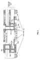
- FIG. 2is a block diagram illustrating a cross sectional view of a multi-layer package with integrated matching networks, in accordance with an embodiment of the invention.
- a chip 201there is shown a chip 201 , an insulating layer 203 , metal layers 205 A, 205 B, 205 C, 207 , 209 , 215 A, 215 B, 215 C and 217 , solder balls 211 , multi-layer package 213 , surface mount components 219 A and 219 B, and thermal epoxy 221 .
- the chip 201may comprise the transceiver 152 described with respect to FIG. 1 , or may also comprise any other integrated circuit within the wireless system 150 that may require impedance matching components and/or devices.
- the chip 201may be bump-bonded or flip-chip bonded to the multi-layer package 213 utilizing the solder balls 211 . In this manner, wire bonds connecting the chip 201 to the multi-layer package 213 may be eliminated, reducing and/or eliminating uncontrollable stray inductances due to wire bonds.
- the thermal conductance out of the chip 201may be greatly improved utilizing the solder balls 211 and the thermal epoxy 221 .
- the thermal epoxy 221may be electrically insulating but thermally conductive to allow for thermal energy to be conducted out of the chip 201 to the much larger thermal mass of the multilayer package 213 .
- the metal layers 205 A, 205 B, 205 C, 207 , 209 , 215 A, 215 B, 215 C and 217may comprise deposited metal layers utilized to delineate impedance matching devices.
- the metal layer 209may be patterned such that it may comprise a transmission line that may be utilized to impedance match a power amplifier in the chip 201 to an antenna, such as the antenna 151 described with respect to FIG. 1 , for example.
- the metal layers 207 and 217may comprise a microstrip structure, the impedance of which may be tuned, for example.
- one or more of the metal layersmay comprise ferromagnetic and/or ferrimagnetic layers utilized to define devices such as transformers, inductors, baluns, isolators, circulators, and gyrators.
- the metal layers 205 A, 205 B, 205 C and 215 Amay comprise a transformer that may be utilized to provide impedance matching between a power amplifier in the chip 201 and an antenna, for example.
- the metal layers 215 Cmay provide electrical contact to the surface mount devices 219 a and 219 B from the chip 201 via the solder balls 211 .
- the number of metal layersmay not be limited to the number of metal layers 205 A, 205 B, 205 C, 207 , 209 , 215 A, 215 B, 215 C and 217 shown in FIG. 2 . Accordingly, there may be any number of layers embedded within the multi-layer package 213 , depending on the number of contacts on the chip 201 coupled to the solder balls 211 , and the number of impedance matching devices fabricated within and/or on the multi-layer package 213 .
- the solder balls 211may comprise spherical balls of metal to provide electrical, thermal and physical contact between the chip 201 and the multi-layer package 213 .
- the chipIn making the contact with the solder balls 211 , the chip may be pressed with enough force to squash the metal spheres somewhat, and may be performed at an elevated temperature to provide suitable electrical resistance and physical bond strength.
- the thermal epoxy 221may fill the volume between the solder balls 211 and may provide a high thermal conductance path for heat transfer out of the chip 201 .
- the solder balls 211may also be utilized to provide electrical, thermal and physical contact between the multi-layer package 213 and a printed circuit board comprising other parts of the wireless system 150 , described with respect to FIG. 1 .
- the surface mount devices 219 A and 219 Bmay comprise discrete circuit elements such as resistors, capacitors, inductors, and diodes, for example.
- the surface mount devices 219 A and 219 Bmay be soldered to the multi-layer package 213 to provide electrical contact.
- the chip 201may comprise an RF front end, such as the RF transceiver 152 , described with respect to FIG. 1 , and may be utilized to transmit and receive RF signals.
- the chip 201may be electrically coupled to impedance matching devices fabricated on and/or within the multi-layer package 213 , such as transformers, baluns, transmission lines, inductors, capacitors and surface mount devices, for example. Heat from the chip 201 may be conducted to the multi-layer package via the thermal epoxy 221 and the solder balls 211 .
- FIG. 3is a block diagram illustrating an exemplary on-package stub matching network, in accordance with an embodiment of the invention.
- a stub matching circuit 300comprising a parallel impedance 301 and a series impedance 303 .
- the stub matching circuit 300may be enabled to match the output impedance 305 , such as from a power amplifier in the chip 201 , for example, and the load impedance 307 , such as from the antenna 151 , described with respect to FIG. 1 .
- the parallel impedance 301 and the series impedance 303may comprise transmission lines, for example, that may be tuned to provide impedance match between the output impedance 305 and the load impedance 307 .
- the transmission linesmay comprise metal layers, such as the metal layer 209 deposited on or embedded within the multi-layer package 213 described with respect to FIG. 2 .
- the parallel impedance 301 and the series impedance 303may comprise microstrip structures, such as the microstrip comprising the metal layers 207 and 217 , described with respect to FIG. 2 , for example.
- the impedancemay be adjusted by changing the dimensions of the structure utilizing microelectromechanical systems (MEMS) switches, for example.
- MEMSmicroelectromechanical systems
- FIG. 4is a block diagram illustrating an exemplary on-package single-ended inductance-network, in accordance with an embodiment of the invention.
- a single-ended inductance (L) network 400comprising an inductor 401 and a variable capacitance 403 .
- the L-network 400may be enabled to match the output impedance 405 , such as from a power amplifier in the chip 201 , for example, and the load impedance 407 , such as from the antenna 151 , described with respect to FIG. 1 .
- the inductor 401may comprise an inductor integrated on the multi-layer package 213 , described with respect to FIG. 2 .
- the inductor 401may comprise a spiral conductor, for example, fabricated from the metal layer 209 , described with respect to FIG. 2 .
- the inductor 401may be fabricated utilizing ferromagnetic material, as described with respect to FIG. 2 .
- the variable capacitor 403may comprise one or more capacitors fabricated on and/or embedded within the multi-layer package 213 , which may be selected by the chip 201 for impedance matching the output impedance 405 with the load resistance 407 .
- Each of the capacitors that comprise the variable capacitor 403may be fabricated from parallel metal layers in the multi-layer package 213 , such as the metal layers 207 and 217 , for example.
- the number of layers comprising the variable capacitor 403is not limited to the number shown in FIG. 2 . Accordingly, any number of individual capacitors may be fabricated as per the capacitance values required for impedance matching.
- FIG. 5is a flow diagram illustrating exemplary steps in the fabrication of matching networks embedded in a multi-layer package, in accordance with an embodiment of the invention.
- the multi-layer packagemay be fabricated with metal conductive and ferromagnetic layers embedded with the structure.
- transmission line and magnetic layer devicesmay be deposited on the top and/or bottom surfaces of the multi-layer package.
- a chipmay be flip-chip bonded to the multi-layer package and the package may then be flip-chip bonded to a printed circuit board. Thermal epoxy may be utilized to fill the volume between the solder balls between the chip and the package.
- the impedances of the impedance matching devices in the multi-layer packagemay be adjusted to match impedances between devices within the chip and external devices, followed by end step 511 .
- a method and systemare disclosed for controlling impedance within an integrated circuit 201 via one or more impedance matching networks 300 , 400 .
- the multi-layer package 213may comprise one or more impedance matching networks 300 , 400 .
- the impedance matching networks 300 , 400may provide impedance matching between devices internal to the integrated circuit 201 and external devices 151 .
- the impedance of one or more devices within the integrated circuit 201may be configured utilizing the impedance matching networks 300 , 400 .
- the impedance matching networks 300 , 400may be embedded within the multi-layer package 213 , and may comprise transmission lines, inductors 401 , capacitors 403 , transformers 205 A, 205 B, 205 C and/or surface mount devices 219 A, 219 B.
- the impedance matching networksmay be deposited on the top of and/or on the bottom of the multi-layer package 213 .
- the integrated circuit 201may be coupled to the multi-layer package 213 utilizing a flip-chip technique.
- Certain embodiments of the inventionmay comprise a machine-readable storage having stored thereon, a computer program having at least one code section for enabling communication, the at least one code section being executable by a machine for causing the machine to perform one or more of the steps described herein.
- aspects of the inventionmay be realized in hardware, software, firmware or a combination thereof.
- the inventionmay be realized in a centralized fashion in at least one computer system or in a distributed fashion where different elements are spread across several interconnected computer systems. Any kind of computer system or other apparatus adapted for carrying out the methods described herein is suited.
- a typical combination of hardware, software and firmwaremay be a general-purpose computer system with a computer program that, when being loaded and executed, controls the computer system such that it carries out the methods described herein.
- One embodiment of the present inventionmay be implemented as a board level product, as a single chip, application specific integrated circuit (ASIC), or with varying levels integrated on a single chip with other portions of the system as separate components.
- the degree of integration of the systemwill primarily be determined by speed and cost considerations. Because of the sophisticated nature of modern processors, it is possible to utilize a commercially available processor, which may be implemented external to an ASIC implementation of the present system. Alternatively, if the processor is available as an ASIC core or logic block, then the commercially available processor may be implemented as part of an ASIC device with various functions implemented as firmware.
- the present inventionmay also be embedded in a computer program product, which comprises all the features enabling the implementation of the methods described herein, and which when loaded in a computer system is able to carry out these methods.
- Computer program in the present contextmay mean, for example, any expression, in any language, code or notation, of a set of instructions intended to cause a system having an information processing capability to perform a particular function either directly or after either or both of the following: a) conversion to another language, code or notation; b) reproduction in a different material form.
- other meanings of computer programwithin the understanding of those skilled in the art are also contemplated by the present invention.
Landscapes
- Engineering & Computer Science (AREA)
- Microelectronics & Electronic Packaging (AREA)
- Physics & Mathematics (AREA)
- Condensed Matter Physics & Semiconductors (AREA)
- General Physics & Mathematics (AREA)
- Computer Hardware Design (AREA)
- Power Engineering (AREA)
- Semiconductor Integrated Circuits (AREA)
- Transceivers (AREA)
Abstract
Description
Claims (22)
Priority Applications (2)
| Application Number | Priority Date | Filing Date | Title |
|---|---|---|---|
| US11/956,071US8115567B2 (en) | 2007-12-13 | 2007-12-13 | Method and system for matching networks embedded in an integrated circuit package |
| US13/345,029US8242858B2 (en) | 2007-12-13 | 2012-01-06 | Method and system for matching networks embedded in an integrated circuit package |
Applications Claiming Priority (1)
| Application Number | Priority Date | Filing Date | Title |
|---|---|---|---|
| US11/956,071US8115567B2 (en) | 2007-12-13 | 2007-12-13 | Method and system for matching networks embedded in an integrated circuit package |
Related Child Applications (1)
| Application Number | Title | Priority Date | Filing Date |
|---|---|---|---|
| US13/345,029ContinuationUS8242858B2 (en) | 2007-12-13 | 2012-01-06 | Method and system for matching networks embedded in an integrated circuit package |
Publications (2)
| Publication Number | Publication Date |
|---|---|
| US20090153261A1 US20090153261A1 (en) | 2009-06-18 |
| US8115567B2true US8115567B2 (en) | 2012-02-14 |
Family
ID=40752407
Family Applications (2)
| Application Number | Title | Priority Date | Filing Date |
|---|---|---|---|
| US11/956,071Expired - Fee RelatedUS8115567B2 (en) | 2007-12-13 | 2007-12-13 | Method and system for matching networks embedded in an integrated circuit package |
| US13/345,029Expired - Fee RelatedUS8242858B2 (en) | 2007-12-13 | 2012-01-06 | Method and system for matching networks embedded in an integrated circuit package |
Family Applications After (1)
| Application Number | Title | Priority Date | Filing Date |
|---|---|---|---|
| US13/345,029Expired - Fee RelatedUS8242858B2 (en) | 2007-12-13 | 2012-01-06 | Method and system for matching networks embedded in an integrated circuit package |
Country Status (1)
| Country | Link |
|---|---|
| US (2) | US8115567B2 (en) |
Families Citing this family (4)
| Publication number | Priority date | Publication date | Assignee | Title |
|---|---|---|---|---|
| EP2387295A1 (en)* | 2010-05-10 | 2011-11-16 | Dialog Semiconductor B.V. | IC-Package with integrated impedance matching and harmonic suppression |
| CN103337717B (en)* | 2013-06-25 | 2015-07-08 | 华为技术有限公司 | Antenna impedance matching device, semiconductor chip and method |
| JP2016071908A (en)* | 2014-09-29 | 2016-05-09 | Tdk株式会社 | Magnetic head, head gimbal assembly, and magnetic recording/reproducing apparatus |
| US20200212536A1 (en)* | 2018-12-31 | 2020-07-02 | Texas Instruments Incorporated | Wireless communication device with antenna on package |
Citations (30)
| Publication number | Priority date | Publication date | Assignee | Title |
|---|---|---|---|---|
| US5914873A (en) | 1997-06-30 | 1999-06-22 | Advanced Micro Devices | Distributed voltage converter apparatus and method for high power microprocessor with array connections |
| US20020039026A1 (en) | 2000-04-04 | 2002-04-04 | Stroth John E. | Power line testing device with signal generator and signal detector |
| US6462976B1 (en) | 1997-02-21 | 2002-10-08 | University Of Arkansas | Conversion of electrical energy from one form to another, and its management through multichip module structures |
| US20020180063A1 (en) | 2001-06-05 | 2002-12-05 | Matsushita Electric Industrial Co., Ltd. | Semiconductor module |
| US6570442B2 (en) | 2000-08-08 | 2003-05-27 | Tdk Corporation | Radio frequency signal output module having radio-frequency power amplifier and isolator element |
| US6590468B2 (en)* | 2000-07-20 | 2003-07-08 | Paratek Microwave, Inc. | Tunable microwave devices with auto-adjusting matching circuit |
| US20040222506A1 (en) | 2002-10-15 | 2004-11-11 | Silicon Laboratories, Inc. | Integrated circuit package configuration incorporating shielded circuit element structure |
| US6848178B2 (en) | 2002-05-30 | 2005-02-01 | Denso Corporation | Enhancement of current-carrying capacity of a multilayer circuit board |
| US20050023656A1 (en) | 2002-08-08 | 2005-02-03 | Leedy Glenn J. | Vertical system integration |
| US20050161753A1 (en) | 2001-05-18 | 2005-07-28 | Corporation For National Research Initiatives | Method of fabricating radio frequency microelectromechanical systems (MEMS) devices on low-temperature co-fired ceramic (LTCC) substrates |
| US20050212642A1 (en) | 2004-03-26 | 2005-09-29 | Harris Corporation | Embedded toroidal transformers in ceramic substrates |
| US20050270135A1 (en) | 2000-05-17 | 2005-12-08 | Xerox Corporation | Method of making photolithographically-patterned out-of-plane coil structures |
| US20060091958A1 (en) | 2004-10-28 | 2006-05-04 | Broadcom Corporation | Multilevel power amplifier architecture using multi-tap transformer |
| US20060152911A1 (en) | 2005-01-10 | 2006-07-13 | Ixys Corporation | Integrated packaged having magnetic components |
| US7084715B2 (en) | 2002-09-27 | 2006-08-01 | Nokia Corporation | Coupling device |
| US7138884B2 (en)* | 2002-08-19 | 2006-11-21 | Dsp Group Inc. | Circuit package integrating passive radio frequency structure |
| US7149496B2 (en) | 2003-03-27 | 2006-12-12 | Kyocera Corporation | High-frequency module and radio communication apparatus |
| US7183633B2 (en) | 2001-03-01 | 2007-02-27 | Analog Devices Inc. | Optical cross-connect system |
| US20070062027A1 (en) | 2005-09-09 | 2007-03-22 | Stmicroelectronics S.R.L. | Inductive structure |
| US7253699B2 (en)* | 2003-05-12 | 2007-08-07 | Hrl Laboratories, Llc | RF MEMS switch with integrated impedance matching structure |
| US7289008B2 (en) | 2003-10-08 | 2007-10-30 | Kyocera Corporation | High-frequency module and communication apparatus |
| US7336232B1 (en) | 2006-08-04 | 2008-02-26 | Raytheon Company | Dual band space-fed array |
| US7348842B2 (en) | 2005-01-19 | 2008-03-25 | Micro-Mobio | Multi-substrate RF module for wireless communication devices |
| US7382213B2 (en)* | 2005-01-28 | 2008-06-03 | Northrop Grumman Corporation | Monolithically integrated switchable circuits with MEMS |
| US7427977B2 (en) | 2003-12-16 | 2008-09-23 | Lg Display Co., Ltd. | Lamp driving device for liquid crystal display device |
| US7515879B2 (en)* | 2004-02-05 | 2009-04-07 | Renesas Technology Corp. | Radio frequency circuit module |
| US7518248B2 (en) | 1999-12-28 | 2009-04-14 | Intel Corporation | Inductive filters and methods of fabrication therefor |
| US20090127674A1 (en) | 2004-06-28 | 2009-05-21 | Mitsubishi Electric Corporation | Multilayer dielectric substrate and semiconductor package |
| US20090189064A1 (en) | 2005-07-26 | 2009-07-30 | Sionex Corporation | Ultra compact ion mobility based analyzer apparatus, method, and system |
| US20090243535A1 (en) | 2008-03-31 | 2009-10-01 | Johnson Controls Technology Company | Multi-Input Relay Board |
- 2007
- 2007-12-13USUS11/956,071patent/US8115567B2/ennot_activeExpired - Fee Related
- 2012
- 2012-01-06USUS13/345,029patent/US8242858B2/ennot_activeExpired - Fee Related
Patent Citations (32)
| Publication number | Priority date | Publication date | Assignee | Title |
|---|---|---|---|---|
| US6462976B1 (en) | 1997-02-21 | 2002-10-08 | University Of Arkansas | Conversion of electrical energy from one form to another, and its management through multichip module structures |
| US5914873A (en) | 1997-06-30 | 1999-06-22 | Advanced Micro Devices | Distributed voltage converter apparatus and method for high power microprocessor with array connections |
| US7518248B2 (en) | 1999-12-28 | 2009-04-14 | Intel Corporation | Inductive filters and methods of fabrication therefor |
| US20020039026A1 (en) | 2000-04-04 | 2002-04-04 | Stroth John E. | Power line testing device with signal generator and signal detector |
| US20050270135A1 (en) | 2000-05-17 | 2005-12-08 | Xerox Corporation | Method of making photolithographically-patterned out-of-plane coil structures |
| US6590468B2 (en)* | 2000-07-20 | 2003-07-08 | Paratek Microwave, Inc. | Tunable microwave devices with auto-adjusting matching circuit |
| US6570442B2 (en) | 2000-08-08 | 2003-05-27 | Tdk Corporation | Radio frequency signal output module having radio-frequency power amplifier and isolator element |
| US7183633B2 (en) | 2001-03-01 | 2007-02-27 | Analog Devices Inc. | Optical cross-connect system |
| US20050161753A1 (en) | 2001-05-18 | 2005-07-28 | Corporation For National Research Initiatives | Method of fabricating radio frequency microelectromechanical systems (MEMS) devices on low-temperature co-fired ceramic (LTCC) substrates |
| US7045440B2 (en) | 2001-05-18 | 2006-05-16 | Corporation For National Research Initiatives | Method of fabricating radio frequency microelectromechanical systems (MEMS) devices on low-temperature co-fired ceramic (LTCC) substrates |
| US7385286B2 (en)* | 2001-06-05 | 2008-06-10 | Matsushita Electric Industrial Co., Ltd. | Semiconductor module |
| US20020180063A1 (en) | 2001-06-05 | 2002-12-05 | Matsushita Electric Industrial Co., Ltd. | Semiconductor module |
| US6848178B2 (en) | 2002-05-30 | 2005-02-01 | Denso Corporation | Enhancement of current-carrying capacity of a multilayer circuit board |
| US20050023656A1 (en) | 2002-08-08 | 2005-02-03 | Leedy Glenn J. | Vertical system integration |
| US7138884B2 (en)* | 2002-08-19 | 2006-11-21 | Dsp Group Inc. | Circuit package integrating passive radio frequency structure |
| US7084715B2 (en) | 2002-09-27 | 2006-08-01 | Nokia Corporation | Coupling device |
| US20040222506A1 (en) | 2002-10-15 | 2004-11-11 | Silicon Laboratories, Inc. | Integrated circuit package configuration incorporating shielded circuit element structure |
| US7149496B2 (en) | 2003-03-27 | 2006-12-12 | Kyocera Corporation | High-frequency module and radio communication apparatus |
| US7253699B2 (en)* | 2003-05-12 | 2007-08-07 | Hrl Laboratories, Llc | RF MEMS switch with integrated impedance matching structure |
| US7289008B2 (en) | 2003-10-08 | 2007-10-30 | Kyocera Corporation | High-frequency module and communication apparatus |
| US7427977B2 (en) | 2003-12-16 | 2008-09-23 | Lg Display Co., Ltd. | Lamp driving device for liquid crystal display device |
| US7515879B2 (en)* | 2004-02-05 | 2009-04-07 | Renesas Technology Corp. | Radio frequency circuit module |
| US20050212642A1 (en) | 2004-03-26 | 2005-09-29 | Harris Corporation | Embedded toroidal transformers in ceramic substrates |
| US20090127674A1 (en) | 2004-06-28 | 2009-05-21 | Mitsubishi Electric Corporation | Multilayer dielectric substrate and semiconductor package |
| US20060091958A1 (en) | 2004-10-28 | 2006-05-04 | Broadcom Corporation | Multilevel power amplifier architecture using multi-tap transformer |
| US20060152911A1 (en) | 2005-01-10 | 2006-07-13 | Ixys Corporation | Integrated packaged having magnetic components |
| US7348842B2 (en) | 2005-01-19 | 2008-03-25 | Micro-Mobio | Multi-substrate RF module for wireless communication devices |
| US7382213B2 (en)* | 2005-01-28 | 2008-06-03 | Northrop Grumman Corporation | Monolithically integrated switchable circuits with MEMS |
| US20090189064A1 (en) | 2005-07-26 | 2009-07-30 | Sionex Corporation | Ultra compact ion mobility based analyzer apparatus, method, and system |
| US20070062027A1 (en) | 2005-09-09 | 2007-03-22 | Stmicroelectronics S.R.L. | Inductive structure |
| US7336232B1 (en) | 2006-08-04 | 2008-02-26 | Raytheon Company | Dual band space-fed array |
| US20090243535A1 (en) | 2008-03-31 | 2009-10-01 | Johnson Controls Technology Company | Multi-Input Relay Board |
Also Published As
| Publication number | Publication date |
|---|---|
| US20090153261A1 (en) | 2009-06-18 |
| US20120105168A1 (en) | 2012-05-03 |
| US8242858B2 (en) | 2012-08-14 |
Similar Documents
| Publication | Publication Date | Title |
|---|---|---|
| US8659369B2 (en) | IC package with embedded filters | |
| US8269344B2 (en) | Method and system for inter-chip communication via integrated circuit package waveguides | |
| US8384596B2 (en) | Method and system for inter-chip communication via integrated circuit package antennas | |
| US8174451B2 (en) | Method and system for configurable antenna in an integrated circuit package | |
| US7863998B2 (en) | Method and system for processing signals via directional couplers embedded in an integrated circuit package | |
| US8855581B2 (en) | Integrated circuit package with transformer | |
| US8198714B2 (en) | Method and system for configuring a transformer embedded in a multi-layer integrated circuit (IC) package | |
| US7859359B2 (en) | Method and system for a balun embedded in an integrated circuit package | |
| US8659366B2 (en) | MEMS switches in an integrated circuit package | |
| US8274147B2 (en) | Method and system for intra-printed circuit board communication via waveguides | |
| US8450846B2 (en) | Method and system for communicating via flip-chip die and package waveguides | |
| US20090219908A1 (en) | Method and system for processing signals via diplexers embedded in an integrated circuit package | |
| US20090153421A1 (en) | Method and system for an integrated antenna and antenna management | |
| US8768269B2 (en) | MEMS and switched capacitors configured for increased resolution switching | |
| US7982555B2 (en) | Method and system for processing signals via power splitters embedded in an integrated circuit package | |
| US8242858B2 (en) | Method and system for matching networks embedded in an integrated circuit package | |
| US7859360B2 (en) | Method and system for controlling MEMS switches in an integrated circuit package |
Legal Events
| Date | Code | Title | Description |
|---|---|---|---|
| AS | Assignment | Owner name:BROADCOM CORPORATION, CALIFORNIA Free format text:ASSIGNMENT OF ASSIGNORS INTEREST;ASSIGNORS:ROFOUGARAN, AHMADREZA;ROFOUGARAN, MARYAM;REEL/FRAME:020553/0201 Effective date:20071211 | |
| ZAAA | Notice of allowance and fees due | Free format text:ORIGINAL CODE: NOA | |
| ZAAB | Notice of allowance mailed | Free format text:ORIGINAL CODE: MN/=. | |
| FEPP | Fee payment procedure | Free format text:PAYOR NUMBER ASSIGNED (ORIGINAL EVENT CODE: ASPN); ENTITY STATUS OF PATENT OWNER: LARGE ENTITY | |
| STCF | Information on status: patent grant | Free format text:PATENTED CASE | |
| FPAY | Fee payment | Year of fee payment:4 | |
| AS | Assignment | Owner name:BANK OF AMERICA, N.A., AS COLLATERAL AGENT, NORTH CAROLINA Free format text:PATENT SECURITY AGREEMENT;ASSIGNOR:BROADCOM CORPORATION;REEL/FRAME:037806/0001 Effective date:20160201 Owner name:BANK OF AMERICA, N.A., AS COLLATERAL AGENT, NORTH Free format text:PATENT SECURITY AGREEMENT;ASSIGNOR:BROADCOM CORPORATION;REEL/FRAME:037806/0001 Effective date:20160201 | |
| AS | Assignment | Owner name:AVAGO TECHNOLOGIES GENERAL IP (SINGAPORE) PTE. LTD., SINGAPORE Free format text:ASSIGNMENT OF ASSIGNORS INTEREST;ASSIGNOR:BROADCOM CORPORATION;REEL/FRAME:041706/0001 Effective date:20170120 Owner name:AVAGO TECHNOLOGIES GENERAL IP (SINGAPORE) PTE. LTD Free format text:ASSIGNMENT OF ASSIGNORS INTEREST;ASSIGNOR:BROADCOM CORPORATION;REEL/FRAME:041706/0001 Effective date:20170120 | |
| AS | Assignment | Owner name:BROADCOM CORPORATION, CALIFORNIA Free format text:TERMINATION AND RELEASE OF SECURITY INTEREST IN PATENTS;ASSIGNOR:BANK OF AMERICA, N.A., AS COLLATERAL AGENT;REEL/FRAME:041712/0001 Effective date:20170119 | |
| AS | Assignment | Owner name:AVAGO TECHNOLOGIES INTERNATIONAL SALES PTE. LIMITE Free format text:MERGER;ASSIGNOR:AVAGO TECHNOLOGIES GENERAL IP (SINGAPORE) PTE. LTD.;REEL/FRAME:047230/0133 Effective date:20180509 | |
| AS | Assignment | Owner name:AVAGO TECHNOLOGIES INTERNATIONAL SALES PTE. LIMITE Free format text:CORRECTIVE ASSIGNMENT TO CORRECT THE EFFECTIVE DATE OF MERGER TO 09/05/2018 PREVIOUSLY RECORDED AT REEL: 047230 FRAME: 0133. ASSIGNOR(S) HEREBY CONFIRMS THE MERGER;ASSIGNOR:AVAGO TECHNOLOGIES GENERAL IP (SINGAPORE) PTE. LTD.;REEL/FRAME:047630/0456 Effective date:20180905 | |
| MAFP | Maintenance fee payment | Free format text:PAYMENT OF MAINTENANCE FEE, 8TH YEAR, LARGE ENTITY (ORIGINAL EVENT CODE: M1552); ENTITY STATUS OF PATENT OWNER: LARGE ENTITY Year of fee payment:8 | |
| FEPP | Fee payment procedure | Free format text:MAINTENANCE FEE REMINDER MAILED (ORIGINAL EVENT CODE: REM.); ENTITY STATUS OF PATENT OWNER: LARGE ENTITY | |
| LAPS | Lapse for failure to pay maintenance fees | Free format text:PATENT EXPIRED FOR FAILURE TO PAY MAINTENANCE FEES (ORIGINAL EVENT CODE: EXP.); ENTITY STATUS OF PATENT OWNER: LARGE ENTITY | |
| STCH | Information on status: patent discontinuation | Free format text:PATENT EXPIRED DUE TO NONPAYMENT OF MAINTENANCE FEES UNDER 37 CFR 1.362 | |
| FP | Lapsed due to failure to pay maintenance fee | Effective date:20240214 |