US8115306B2 - Apparatus and method for packaging circuits - Google Patents
Apparatus and method for packaging circuitsDownload PDFInfo
- Publication number
- US8115306B2 US8115306B2US12/705,277US70527710AUS8115306B2US 8115306 B2US8115306 B2US 8115306B2US 70527710 AUS70527710 AUS 70527710AUS 8115306 B2US8115306 B2US 8115306B2
- Authority
- US
- United States
- Prior art keywords
- contact
- edge
- die
- edge contact
- dice
- Prior art date
- Legal status (The legal status is an assumption and is not a legal conclusion. Google has not performed a legal analysis and makes no representation as to the accuracy of the status listed.)
- Expired - Fee Related
Links
Images


Classifications
- H—ELECTRICITY
- H01—ELECTRIC ELEMENTS
- H01L—SEMICONDUCTOR DEVICES NOT COVERED BY CLASS H10
- H01L21/00—Processes or apparatus adapted for the manufacture or treatment of semiconductor or solid state devices or of parts thereof
- H01L21/70—Manufacture or treatment of devices consisting of a plurality of solid state components formed in or on a common substrate or of parts thereof; Manufacture of integrated circuit devices or of parts thereof
- H01L21/77—Manufacture or treatment of devices consisting of a plurality of solid state components or integrated circuits formed in, or on, a common substrate
- H01L21/78—Manufacture or treatment of devices consisting of a plurality of solid state components or integrated circuits formed in, or on, a common substrate with subsequent division of the substrate into plural individual devices
- H—ELECTRICITY
- H01—ELECTRIC ELEMENTS
- H01L—SEMICONDUCTOR DEVICES NOT COVERED BY CLASS H10
- H01L24/00—Arrangements for connecting or disconnecting semiconductor or solid-state bodies; Methods or apparatus related thereto
- H01L24/01—Means for bonding being attached to, or being formed on, the surface to be connected, e.g. chip-to-package, die-attach, "first-level" interconnects; Manufacturing methods related thereto
- H01L24/02—Bonding areas ; Manufacturing methods related thereto
- H01L24/03—Manufacturing methods
- H—ELECTRICITY
- H01—ELECTRIC ELEMENTS
- H01L—SEMICONDUCTOR DEVICES NOT COVERED BY CLASS H10
- H01L24/00—Arrangements for connecting or disconnecting semiconductor or solid-state bodies; Methods or apparatus related thereto
- H01L24/01—Means for bonding being attached to, or being formed on, the surface to be connected, e.g. chip-to-package, die-attach, "first-level" interconnects; Manufacturing methods related thereto
- H01L24/02—Bonding areas ; Manufacturing methods related thereto
- H01L24/04—Structure, shape, material or disposition of the bonding areas prior to the connecting process
- H01L24/05—Structure, shape, material or disposition of the bonding areas prior to the connecting process of an individual bonding area
- H—ELECTRICITY
- H01—ELECTRIC ELEMENTS
- H01L—SEMICONDUCTOR DEVICES NOT COVERED BY CLASS H10
- H01L24/00—Arrangements for connecting or disconnecting semiconductor or solid-state bodies; Methods or apparatus related thereto
- H01L24/93—Batch processes
- H—ELECTRICITY
- H10—SEMICONDUCTOR DEVICES; ELECTRIC SOLID-STATE DEVICES NOT OTHERWISE PROVIDED FOR
- H10B—ELECTRONIC MEMORY DEVICES
- H10B99/00—Subject matter not provided for in other groups of this subclass
- H10B99/22—Subject matter not provided for in other groups of this subclass including field-effect components
- H—ELECTRICITY
- H01—ELECTRIC ELEMENTS
- H01L—SEMICONDUCTOR DEVICES NOT COVERED BY CLASS H10
- H01L2224/00—Indexing scheme for arrangements for connecting or disconnecting semiconductor or solid-state bodies and methods related thereto as covered by H01L24/00
- H01L2224/01—Means for bonding being attached to, or being formed on, the surface to be connected, e.g. chip-to-package, die-attach, "first-level" interconnects; Manufacturing methods related thereto
- H01L2224/02—Bonding areas; Manufacturing methods related thereto
- H01L2224/023—Redistribution layers [RDL] for bonding areas
- H01L2224/0231—Manufacturing methods of the redistribution layers
- H01L2224/02311—Additive methods
- H—ELECTRICITY
- H01—ELECTRIC ELEMENTS
- H01L—SEMICONDUCTOR DEVICES NOT COVERED BY CLASS H10
- H01L2224/00—Indexing scheme for arrangements for connecting or disconnecting semiconductor or solid-state bodies and methods related thereto as covered by H01L24/00
- H01L2224/01—Means for bonding being attached to, or being formed on, the surface to be connected, e.g. chip-to-package, die-attach, "first-level" interconnects; Manufacturing methods related thereto
- H01L2224/02—Bonding areas; Manufacturing methods related thereto
- H01L2224/023—Redistribution layers [RDL] for bonding areas
- H01L2224/0231—Manufacturing methods of the redistribution layers
- H01L2224/02313—Subtractive methods
- H—ELECTRICITY
- H01—ELECTRIC ELEMENTS
- H01L—SEMICONDUCTOR DEVICES NOT COVERED BY CLASS H10
- H01L2224/00—Indexing scheme for arrangements for connecting or disconnecting semiconductor or solid-state bodies and methods related thereto as covered by H01L24/00
- H01L2224/01—Means for bonding being attached to, or being formed on, the surface to be connected, e.g. chip-to-package, die-attach, "first-level" interconnects; Manufacturing methods related thereto
- H01L2224/02—Bonding areas; Manufacturing methods related thereto
- H01L2224/023—Redistribution layers [RDL] for bonding areas
- H01L2224/0233—Structure of the redistribution layers
- H01L2224/02331—Multilayer structure
- H—ELECTRICITY
- H01—ELECTRIC ELEMENTS
- H01L—SEMICONDUCTOR DEVICES NOT COVERED BY CLASS H10
- H01L2224/00—Indexing scheme for arrangements for connecting or disconnecting semiconductor or solid-state bodies and methods related thereto as covered by H01L24/00
- H01L2224/01—Means for bonding being attached to, or being formed on, the surface to be connected, e.g. chip-to-package, die-attach, "first-level" interconnects; Manufacturing methods related thereto
- H01L2224/02—Bonding areas; Manufacturing methods related thereto
- H01L2224/023—Redistribution layers [RDL] for bonding areas
- H01L2224/0237—Disposition of the redistribution layers
- H01L2224/02371—Disposition of the redistribution layers connecting the bonding area on a surface of the semiconductor or solid-state body with another surface of the semiconductor or solid-state body
- H—ELECTRICITY
- H01—ELECTRIC ELEMENTS
- H01L—SEMICONDUCTOR DEVICES NOT COVERED BY CLASS H10
- H01L2224/00—Indexing scheme for arrangements for connecting or disconnecting semiconductor or solid-state bodies and methods related thereto as covered by H01L24/00
- H01L2224/01—Means for bonding being attached to, or being formed on, the surface to be connected, e.g. chip-to-package, die-attach, "first-level" interconnects; Manufacturing methods related thereto
- H01L2224/02—Bonding areas; Manufacturing methods related thereto
- H01L2224/023—Redistribution layers [RDL] for bonding areas
- H01L2224/0237—Disposition of the redistribution layers
- H01L2224/02375—Top view
- H—ELECTRICITY
- H01—ELECTRIC ELEMENTS
- H01L—SEMICONDUCTOR DEVICES NOT COVERED BY CLASS H10
- H01L2224/00—Indexing scheme for arrangements for connecting or disconnecting semiconductor or solid-state bodies and methods related thereto as covered by H01L24/00
- H01L2224/01—Means for bonding being attached to, or being formed on, the surface to be connected, e.g. chip-to-package, die-attach, "first-level" interconnects; Manufacturing methods related thereto
- H01L2224/02—Bonding areas; Manufacturing methods related thereto
- H01L2224/023—Redistribution layers [RDL] for bonding areas
- H01L2224/0237—Disposition of the redistribution layers
- H01L2224/02379—Fan-out arrangement
- H—ELECTRICITY
- H01—ELECTRIC ELEMENTS
- H01L—SEMICONDUCTOR DEVICES NOT COVERED BY CLASS H10
- H01L2224/00—Indexing scheme for arrangements for connecting or disconnecting semiconductor or solid-state bodies and methods related thereto as covered by H01L24/00
- H01L2224/01—Means for bonding being attached to, or being formed on, the surface to be connected, e.g. chip-to-package, die-attach, "first-level" interconnects; Manufacturing methods related thereto
- H01L2224/02—Bonding areas; Manufacturing methods related thereto
- H01L2224/023—Redistribution layers [RDL] for bonding areas
- H01L2224/0239—Material of the redistribution layers
- H—ELECTRICITY
- H01—ELECTRIC ELEMENTS
- H01L—SEMICONDUCTOR DEVICES NOT COVERED BY CLASS H10
- H01L2224/00—Indexing scheme for arrangements for connecting or disconnecting semiconductor or solid-state bodies and methods related thereto as covered by H01L24/00
- H01L2224/01—Means for bonding being attached to, or being formed on, the surface to be connected, e.g. chip-to-package, die-attach, "first-level" interconnects; Manufacturing methods related thereto
- H01L2224/02—Bonding areas; Manufacturing methods related thereto
- H01L2224/03—Manufacturing methods
- H01L2224/034—Manufacturing methods by blanket deposition of the material of the bonding area
- H01L2224/03444—Manufacturing methods by blanket deposition of the material of the bonding area in gaseous form
- H01L2224/0345—Physical vapour deposition [PVD], e.g. evaporation, or sputtering
- H—ELECTRICITY
- H01—ELECTRIC ELEMENTS
- H01L—SEMICONDUCTOR DEVICES NOT COVERED BY CLASS H10
- H01L2224/00—Indexing scheme for arrangements for connecting or disconnecting semiconductor or solid-state bodies and methods related thereto as covered by H01L24/00
- H01L2224/01—Means for bonding being attached to, or being formed on, the surface to be connected, e.g. chip-to-package, die-attach, "first-level" interconnects; Manufacturing methods related thereto
- H01L2224/02—Bonding areas; Manufacturing methods related thereto
- H01L2224/03—Manufacturing methods
- H01L2224/034—Manufacturing methods by blanket deposition of the material of the bonding area
- H01L2224/03444—Manufacturing methods by blanket deposition of the material of the bonding area in gaseous form
- H01L2224/03452—Chemical vapour deposition [CVD], e.g. laser CVD
- H—ELECTRICITY
- H01—ELECTRIC ELEMENTS
- H01L—SEMICONDUCTOR DEVICES NOT COVERED BY CLASS H10
- H01L2224/00—Indexing scheme for arrangements for connecting or disconnecting semiconductor or solid-state bodies and methods related thereto as covered by H01L24/00
- H01L2224/01—Means for bonding being attached to, or being formed on, the surface to be connected, e.g. chip-to-package, die-attach, "first-level" interconnects; Manufacturing methods related thereto
- H01L2224/02—Bonding areas; Manufacturing methods related thereto
- H01L2224/03—Manufacturing methods
- H01L2224/036—Manufacturing methods by patterning a pre-deposited material
- H01L2224/0361—Physical or chemical etching
- H—ELECTRICITY
- H01—ELECTRIC ELEMENTS
- H01L—SEMICONDUCTOR DEVICES NOT COVERED BY CLASS H10
- H01L2224/00—Indexing scheme for arrangements for connecting or disconnecting semiconductor or solid-state bodies and methods related thereto as covered by H01L24/00
- H01L2224/01—Means for bonding being attached to, or being formed on, the surface to be connected, e.g. chip-to-package, die-attach, "first-level" interconnects; Manufacturing methods related thereto
- H01L2224/02—Bonding areas; Manufacturing methods related thereto
- H01L2224/03—Manufacturing methods
- H01L2224/036—Manufacturing methods by patterning a pre-deposited material
- H01L2224/03622—Manufacturing methods by patterning a pre-deposited material using masks
- H—ELECTRICITY
- H01—ELECTRIC ELEMENTS
- H01L—SEMICONDUCTOR DEVICES NOT COVERED BY CLASS H10
- H01L2224/00—Indexing scheme for arrangements for connecting or disconnecting semiconductor or solid-state bodies and methods related thereto as covered by H01L24/00
- H01L2224/01—Means for bonding being attached to, or being formed on, the surface to be connected, e.g. chip-to-package, die-attach, "first-level" interconnects; Manufacturing methods related thereto
- H01L2224/02—Bonding areas; Manufacturing methods related thereto
- H01L2224/03—Manufacturing methods
- H01L2224/039—Methods of manufacturing bonding areas involving a specific sequence of method steps
- H—ELECTRICITY
- H01—ELECTRIC ELEMENTS
- H01L—SEMICONDUCTOR DEVICES NOT COVERED BY CLASS H10
- H01L2224/00—Indexing scheme for arrangements for connecting or disconnecting semiconductor or solid-state bodies and methods related thereto as covered by H01L24/00
- H01L2224/01—Means for bonding being attached to, or being formed on, the surface to be connected, e.g. chip-to-package, die-attach, "first-level" interconnects; Manufacturing methods related thereto
- H01L2224/02—Bonding areas; Manufacturing methods related thereto
- H01L2224/04—Structure, shape, material or disposition of the bonding areas prior to the connecting process
- H01L2224/05—Structure, shape, material or disposition of the bonding areas prior to the connecting process of an individual bonding area
- H01L2224/0554—External layer
- H01L2224/05541—Structure
- H01L2224/05548—Bonding area integrally formed with a redistribution layer on the semiconductor or solid-state body
- H—ELECTRICITY
- H01—ELECTRIC ELEMENTS
- H01L—SEMICONDUCTOR DEVICES NOT COVERED BY CLASS H10
- H01L2224/00—Indexing scheme for arrangements for connecting or disconnecting semiconductor or solid-state bodies and methods related thereto as covered by H01L24/00
- H01L2224/01—Means for bonding being attached to, or being formed on, the surface to be connected, e.g. chip-to-package, die-attach, "first-level" interconnects; Manufacturing methods related thereto
- H01L2224/02—Bonding areas; Manufacturing methods related thereto
- H01L2224/04—Structure, shape, material or disposition of the bonding areas prior to the connecting process
- H01L2224/05—Structure, shape, material or disposition of the bonding areas prior to the connecting process of an individual bonding area
- H01L2224/0554—External layer
- H01L2224/0556—Disposition
- H01L2224/05569—Disposition the external layer being disposed on a redistribution layer on the semiconductor or solid-state body
- H—ELECTRICITY
- H01—ELECTRIC ELEMENTS
- H01L—SEMICONDUCTOR DEVICES NOT COVERED BY CLASS H10
- H01L2224/00—Indexing scheme for arrangements for connecting or disconnecting semiconductor or solid-state bodies and methods related thereto as covered by H01L24/00
- H01L2224/01—Means for bonding being attached to, or being formed on, the surface to be connected, e.g. chip-to-package, die-attach, "first-level" interconnects; Manufacturing methods related thereto
- H01L2224/02—Bonding areas; Manufacturing methods related thereto
- H01L2224/04—Structure, shape, material or disposition of the bonding areas prior to the connecting process
- H01L2224/05—Structure, shape, material or disposition of the bonding areas prior to the connecting process of an individual bonding area
- H01L2224/0554—External layer
- H01L2224/0556—Disposition
- H01L2224/05571—Disposition the external layer being disposed in a recess of the surface
- H01L2224/05572—Disposition the external layer being disposed in a recess of the surface the external layer extending out of an opening
- H—ELECTRICITY
- H01—ELECTRIC ELEMENTS
- H01L—SEMICONDUCTOR DEVICES NOT COVERED BY CLASS H10
- H01L2224/00—Indexing scheme for arrangements for connecting or disconnecting semiconductor or solid-state bodies and methods related thereto as covered by H01L24/00
- H01L2224/01—Means for bonding being attached to, or being formed on, the surface to be connected, e.g. chip-to-package, die-attach, "first-level" interconnects; Manufacturing methods related thereto
- H01L2224/02—Bonding areas; Manufacturing methods related thereto
- H01L2224/04—Structure, shape, material or disposition of the bonding areas prior to the connecting process
- H01L2224/05—Structure, shape, material or disposition of the bonding areas prior to the connecting process of an individual bonding area
- H01L2224/0554—External layer
- H01L2224/05599—Material
- H01L2224/056—Material with a principal constituent of the material being a metal or a metalloid, e.g. boron [B], silicon [Si], germanium [Ge], arsenic [As], antimony [Sb], tellurium [Te] and polonium [Po], and alloys thereof
- H—ELECTRICITY
- H01—ELECTRIC ELEMENTS
- H01L—SEMICONDUCTOR DEVICES NOT COVERED BY CLASS H10
- H01L2224/00—Indexing scheme for arrangements for connecting or disconnecting semiconductor or solid-state bodies and methods related thereto as covered by H01L24/00
- H01L2224/01—Means for bonding being attached to, or being formed on, the surface to be connected, e.g. chip-to-package, die-attach, "first-level" interconnects; Manufacturing methods related thereto
- H01L2224/02—Bonding areas; Manufacturing methods related thereto
- H01L2224/07—Structure, shape, material or disposition of the bonding areas after the connecting process
- H01L2224/08—Structure, shape, material or disposition of the bonding areas after the connecting process of an individual bonding area
- H01L2224/081—Disposition
- H01L2224/0812—Disposition the bonding area connecting directly to another bonding area, i.e. connectorless bonding, e.g. bumpless bonding
- H01L2224/08151—Disposition the bonding area connecting directly to another bonding area, i.e. connectorless bonding, e.g. bumpless bonding the bonding area connecting between a semiconductor or solid-state body and an item not being a semiconductor or solid-state body, e.g. chip-to-substrate, chip-to-passive
- H01L2224/08221—Disposition the bonding area connecting directly to another bonding area, i.e. connectorless bonding, e.g. bumpless bonding the bonding area connecting between a semiconductor or solid-state body and an item not being a semiconductor or solid-state body, e.g. chip-to-substrate, chip-to-passive the body and the item being stacked
- H01L2224/08225—Disposition the bonding area connecting directly to another bonding area, i.e. connectorless bonding, e.g. bumpless bonding the bonding area connecting between a semiconductor or solid-state body and an item not being a semiconductor or solid-state body, e.g. chip-to-substrate, chip-to-passive the body and the item being stacked the item being non-metallic, e.g. insulating substrate with or without metallisation
- H01L2224/08237—Disposition the bonding area connecting directly to another bonding area, i.e. connectorless bonding, e.g. bumpless bonding the bonding area connecting between a semiconductor or solid-state body and an item not being a semiconductor or solid-state body, e.g. chip-to-substrate, chip-to-passive the body and the item being stacked the item being non-metallic, e.g. insulating substrate with or without metallisation the bonding area connecting to a bonding area disposed in a recess of the surface of the item
- H—ELECTRICITY
- H01—ELECTRIC ELEMENTS
- H01L—SEMICONDUCTOR DEVICES NOT COVERED BY CLASS H10
- H01L2224/00—Indexing scheme for arrangements for connecting or disconnecting semiconductor or solid-state bodies and methods related thereto as covered by H01L24/00
- H01L2224/80—Methods for connecting semiconductor or other solid state bodies using means for bonding being attached to, or being formed on, the surface to be connected
- H01L2224/80001—Methods for connecting semiconductor or other solid state bodies using means for bonding being attached to, or being formed on, the surface to be connected by connecting a bonding area directly to another bonding area, i.e. connectorless bonding, e.g. bumpless bonding
- H01L2224/8034—Bonding interfaces of the bonding area
- H01L2224/80357—Bonding interfaces of the bonding area being flush with the surface
- H—ELECTRICITY
- H01—ELECTRIC ELEMENTS
- H01L—SEMICONDUCTOR DEVICES NOT COVERED BY CLASS H10
- H01L2224/00—Indexing scheme for arrangements for connecting or disconnecting semiconductor or solid-state bodies and methods related thereto as covered by H01L24/00
- H01L2224/80—Methods for connecting semiconductor or other solid state bodies using means for bonding being attached to, or being formed on, the surface to be connected
- H01L2224/80001—Methods for connecting semiconductor or other solid state bodies using means for bonding being attached to, or being formed on, the surface to be connected by connecting a bonding area directly to another bonding area, i.e. connectorless bonding, e.g. bumpless bonding
- H01L2224/8038—Bonding interfaces outside the semiconductor or solid-state body
- H01L2224/80399—Material
- H01L2224/804—Material with a principal constituent of the material being a metal or a metalloid, e.g. boron [B], silicon [Si], germanium [Ge], arsenic [As], antimony [Sb], tellurium [Te] and polonium [Po], and alloys thereof
- H—ELECTRICITY
- H01—ELECTRIC ELEMENTS
- H01L—SEMICONDUCTOR DEVICES NOT COVERED BY CLASS H10
- H01L2224/00—Indexing scheme for arrangements for connecting or disconnecting semiconductor or solid-state bodies and methods related thereto as covered by H01L24/00
- H01L2224/80—Methods for connecting semiconductor or other solid state bodies using means for bonding being attached to, or being formed on, the surface to be connected
- H01L2224/80001—Methods for connecting semiconductor or other solid state bodies using means for bonding being attached to, or being formed on, the surface to be connected by connecting a bonding area directly to another bonding area, i.e. connectorless bonding, e.g. bumpless bonding
- H01L2224/808—Bonding techniques
- H01L2224/80897—Mechanical interlocking, e.g. anchoring, hook and loop-type fastening or the like
- H01L2224/80898—Press-fitting, i.e. pushing the parts together and fastening by friction, e.g. by compression of one part against the other
- H—ELECTRICITY
- H01—ELECTRIC ELEMENTS
- H01L—SEMICONDUCTOR DEVICES NOT COVERED BY CLASS H10
- H01L2224/00—Indexing scheme for arrangements for connecting or disconnecting semiconductor or solid-state bodies and methods related thereto as covered by H01L24/00
- H01L2224/93—Batch processes
- H—ELECTRICITY
- H01—ELECTRIC ELEMENTS
- H01L—SEMICONDUCTOR DEVICES NOT COVERED BY CLASS H10
- H01L24/00—Arrangements for connecting or disconnecting semiconductor or solid-state bodies; Methods or apparatus related thereto
- H01L24/01—Means for bonding being attached to, or being formed on, the surface to be connected, e.g. chip-to-package, die-attach, "first-level" interconnects; Manufacturing methods related thereto
- H01L24/02—Bonding areas ; Manufacturing methods related thereto
- H01L24/07—Structure, shape, material or disposition of the bonding areas after the connecting process
- H01L24/08—Structure, shape, material or disposition of the bonding areas after the connecting process of an individual bonding area
- H—ELECTRICITY
- H01—ELECTRIC ELEMENTS
- H01L—SEMICONDUCTOR DEVICES NOT COVERED BY CLASS H10
- H01L24/00—Arrangements for connecting or disconnecting semiconductor or solid-state bodies; Methods or apparatus related thereto
- H01L24/80—Methods for connecting semiconductor or other solid state bodies using means for bonding being attached to, or being formed on, the surface to be connected
- H—ELECTRICITY
- H01—ELECTRIC ELEMENTS
- H01L—SEMICONDUCTOR DEVICES NOT COVERED BY CLASS H10
- H01L2924/00—Indexing scheme for arrangements or methods for connecting or disconnecting semiconductor or solid-state bodies as covered by H01L24/00
- H01L2924/0001—Technical content checked by a classifier
- H01L2924/0002—Not covered by any one of groups H01L24/00, H01L24/00 and H01L2224/00
- H—ELECTRICITY
- H01—ELECTRIC ELEMENTS
- H01L—SEMICONDUCTOR DEVICES NOT COVERED BY CLASS H10
- H01L2924/00—Indexing scheme for arrangements or methods for connecting or disconnecting semiconductor or solid-state bodies as covered by H01L24/00
- H01L2924/01—Chemical elements
- H01L2924/01006—Carbon [C]
- H—ELECTRICITY
- H01—ELECTRIC ELEMENTS
- H01L—SEMICONDUCTOR DEVICES NOT COVERED BY CLASS H10
- H01L2924/00—Indexing scheme for arrangements or methods for connecting or disconnecting semiconductor or solid-state bodies as covered by H01L24/00
- H01L2924/01—Chemical elements
- H01L2924/01014—Silicon [Si]
- H—ELECTRICITY
- H01—ELECTRIC ELEMENTS
- H01L—SEMICONDUCTOR DEVICES NOT COVERED BY CLASS H10
- H01L2924/00—Indexing scheme for arrangements or methods for connecting or disconnecting semiconductor or solid-state bodies as covered by H01L24/00
- H01L2924/01—Chemical elements
- H01L2924/01015—Phosphorus [P]
- H—ELECTRICITY
- H01—ELECTRIC ELEMENTS
- H01L—SEMICONDUCTOR DEVICES NOT COVERED BY CLASS H10
- H01L2924/00—Indexing scheme for arrangements or methods for connecting or disconnecting semiconductor or solid-state bodies as covered by H01L24/00
- H01L2924/01—Chemical elements
- H01L2924/01022—Titanium [Ti]
- H—ELECTRICITY
- H01—ELECTRIC ELEMENTS
- H01L—SEMICONDUCTOR DEVICES NOT COVERED BY CLASS H10
- H01L2924/00—Indexing scheme for arrangements or methods for connecting or disconnecting semiconductor or solid-state bodies as covered by H01L24/00
- H01L2924/01—Chemical elements
- H01L2924/01029—Copper [Cu]
- H—ELECTRICITY
- H01—ELECTRIC ELEMENTS
- H01L—SEMICONDUCTOR DEVICES NOT COVERED BY CLASS H10
- H01L2924/00—Indexing scheme for arrangements or methods for connecting or disconnecting semiconductor or solid-state bodies as covered by H01L24/00
- H01L2924/01—Chemical elements
- H01L2924/01033—Arsenic [As]
- H—ELECTRICITY
- H01—ELECTRIC ELEMENTS
- H01L—SEMICONDUCTOR DEVICES NOT COVERED BY CLASS H10
- H01L2924/00—Indexing scheme for arrangements or methods for connecting or disconnecting semiconductor or solid-state bodies as covered by H01L24/00
- H01L2924/01—Chemical elements
- H01L2924/01047—Silver [Ag]
- H—ELECTRICITY
- H01—ELECTRIC ELEMENTS
- H01L—SEMICONDUCTOR DEVICES NOT COVERED BY CLASS H10
- H01L2924/00—Indexing scheme for arrangements or methods for connecting or disconnecting semiconductor or solid-state bodies as covered by H01L24/00
- H01L2924/01—Chemical elements
- H01L2924/01074—Tungsten [W]
- H—ELECTRICITY
- H01—ELECTRIC ELEMENTS
- H01L—SEMICONDUCTOR DEVICES NOT COVERED BY CLASS H10
- H01L2924/00—Indexing scheme for arrangements or methods for connecting or disconnecting semiconductor or solid-state bodies as covered by H01L24/00
- H01L2924/01—Chemical elements
- H01L2924/01079—Gold [Au]
- H—ELECTRICITY
- H01—ELECTRIC ELEMENTS
- H01L—SEMICONDUCTOR DEVICES NOT COVERED BY CLASS H10
- H01L2924/00—Indexing scheme for arrangements or methods for connecting or disconnecting semiconductor or solid-state bodies as covered by H01L24/00
- H01L2924/01—Chemical elements
- H01L2924/01082—Lead [Pb]
- H—ELECTRICITY
- H01—ELECTRIC ELEMENTS
- H01L—SEMICONDUCTOR DEVICES NOT COVERED BY CLASS H10
- H01L2924/00—Indexing scheme for arrangements or methods for connecting or disconnecting semiconductor or solid-state bodies as covered by H01L24/00
- H01L2924/013—Alloys
- H01L2924/014—Solder alloys
- H—ELECTRICITY
- H01—ELECTRIC ELEMENTS
- H01L—SEMICONDUCTOR DEVICES NOT COVERED BY CLASS H10
- H01L2924/00—Indexing scheme for arrangements or methods for connecting or disconnecting semiconductor or solid-state bodies as covered by H01L24/00
- H01L2924/049—Nitrides composed of metals from groups of the periodic table
- H01L2924/0504—14th Group
- H01L2924/05042—Si3N4
- H—ELECTRICITY
- H01—ELECTRIC ELEMENTS
- H01L—SEMICONDUCTOR DEVICES NOT COVERED BY CLASS H10
- H01L2924/00—Indexing scheme for arrangements or methods for connecting or disconnecting semiconductor or solid-state bodies as covered by H01L24/00
- H01L2924/10—Details of semiconductor or other solid state devices to be connected
- H01L2924/1015—Shape
- H01L2924/10155—Shape being other than a cuboid
- H01L2924/10156—Shape being other than a cuboid at the periphery
- H—ELECTRICITY
- H01—ELECTRIC ELEMENTS
- H01L—SEMICONDUCTOR DEVICES NOT COVERED BY CLASS H10
- H01L2924/00—Indexing scheme for arrangements or methods for connecting or disconnecting semiconductor or solid-state bodies as covered by H01L24/00
- H01L2924/10—Details of semiconductor or other solid state devices to be connected
- H01L2924/11—Device type
- H01L2924/12—Passive devices, e.g. 2 terminal devices
- H01L2924/1204—Optical Diode
- H01L2924/12042—LASER
- H—ELECTRICITY
- H01—ELECTRIC ELEMENTS
- H01L—SEMICONDUCTOR DEVICES NOT COVERED BY CLASS H10
- H01L2924/00—Indexing scheme for arrangements or methods for connecting or disconnecting semiconductor or solid-state bodies as covered by H01L24/00
- H01L2924/10—Details of semiconductor or other solid state devices to be connected
- H01L2924/11—Device type
- H01L2924/14—Integrated circuits
- H—ELECTRICITY
- H01—ELECTRIC ELEMENTS
- H01L—SEMICONDUCTOR DEVICES NOT COVERED BY CLASS H10
- H01L2924/00—Indexing scheme for arrangements or methods for connecting or disconnecting semiconductor or solid-state bodies as covered by H01L24/00
- H01L2924/15—Details of package parts other than the semiconductor or other solid state devices to be connected
- H01L2924/151—Die mounting substrate
- H01L2924/1515—Shape
- H01L2924/15153—Shape the die mounting substrate comprising a recess for hosting the device
- H—ELECTRICITY
- H01—ELECTRIC ELEMENTS
- H01L—SEMICONDUCTOR DEVICES NOT COVERED BY CLASS H10
- H01L2924/00—Indexing scheme for arrangements or methods for connecting or disconnecting semiconductor or solid-state bodies as covered by H01L24/00
- H01L2924/19—Details of hybrid assemblies other than the semiconductor or other solid state devices to be connected
- H01L2924/1901—Structure
- H01L2924/1904—Component type
- H01L2924/19041—Component type being a capacitor
Definitions
- Wafersare fabricated with a plurality of dice each having a plurality of integrated circuit elements therein.
- a dierepresents one individual chip that must be separated from adjacent dice before packaging.
- Contactsare added to the die before packaging.
- One type of contactis a solder ball.
- Wafer level packagingrefers to the complete packaging of an electronic component at the die or the wafer level. WLP is normally considered as a true chip size package. However, the profile of most WLP is the sum of the thickness of the die and the solder balls. It is desired to reduce the profile and/or thickness of packaged components.
- An embodiment of the inventionincludes an edge contact at a peripheral surface of the die.
- the edge contactconnects to a bond pad through a line.
- adjacent dice on a waferare connected to a same edge contact.
- the edge contactis divided.
- the edge contactis divided when the dice are separated.
- the edge contactis in the saw street and is divided when the wafer is diced.
- the diein some embodiments, includes a main body including a top layer, a bottom layer, and a peripheral edge surface extending between the top layer and the bottom layer.
- the main bodyincludes an integrated circuit therein that is electrically connected to the bond pad.
- the edge contactis beneath the top layer.
- the edge contactis above the bottom layer such that the edge contact does not increase the height of the die.
- the bond padis at the top layer.
- the dieis encased by an encapsulant.
- Some embodiments of the inventioninclude methods for creating a die.
- An embodiment of the inventionincludes fabricating at least two dice on a wafer, wherein the at least two dice are joined at an electrically conductive element in a saw street, and separating the at least two dice from each other along the saw street. At least part of the electrically conductive element remains with each die.
- the electrically conductive elementis created by forming a recess in the saw street and filling the recess with an electrically conducting material.
- the methodincludes connecting a bond pad from at least one of the dice to the electrically conductive material.
- An embodiment of the inventionincludes fabricating circuits for a memory device in at least one of the dice.
- forming the recessincludes sawing along the saw street to a depth of about half a height of the die.
- An embodiment of the inventionincludes connecting the bond pad includes depositing a metal on the wafer between the bond pad and the electrically conductive material.
- a further embodiment of the methodincludes patterning a recess in a saw street intermediate adjacent dice in a wafer, depositing an electrically conductive material in the recess to form an edge contact, connecting a bond pad of both dice to the edge contact, and separating the adjacent dice along the saw street such that each dice includes a part of the edge contact.
- An embodiment of the inventionincludes masking the wafer such that the electrically conductive material is deposited only in the recess.
- Embodiments of the inventionalso include substrates, wafers, integrated circuit packages, electrical devices, memory units, memory modules, electrical systems, computers, which include at least one die.
- FIG. 1is a top view of a wafer including a plurality of dice according to the invention.
- FIG. 2is a perspective view of a die according to the invention.
- FIGS. 3A and 3Bare cross sectional views of two dice according to an embodiment of the invention.
- FIGS. 3C and 3Dare cross sectional views of two dice according to an embodiment of the invention.
- FIGS. 4A , 4 B, and 4 Care cross sectional views of two dice according to an embodiment of the invention.
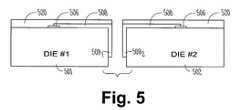
- FIG. 5is a view of two dice separated according to the teachings of an embodiment of the invention.
- FIG. 6is a top view of a die in a package according to the teachings of an embodiment of the invention.
- FIG. 7is a view of a circuit module according to the teachings of an embodiment of the invention.
- FIG. 8is view of a memory module according to the teachings of an embodiment of the invention.
- FIG. 9is a view of an electronic system according to the teachings of an embodiment of the invention.
- FIG. 10is a view of an embodiment of an electronic system according to the teachings an embodiment of the invention.
- FIG. 11is a view of a computer system according to the teachings of an embodiment of the invention.
- wafer and substrate used in the following descriptioninclude any base semiconductor structure. Both are to be understood as including silicon-on-sapphire (SOS) technology, silicon-on-insulator (SOI) technology, thin film transistor (TFT) technology, doped and undoped semiconductors, epitaxial layers of a silicon supported by a base semiconductor structure, as well as other semiconductor structures well known to one skilled in the art.
- SOSsilicon-on-sapphire
- SOIsilicon-on-insulator
- TFTthin film transistor
- the present descriptionuses a reference number convention of the first digit corresponding to the figure in which the number references and the last two digits corresponding to like elements throughout the description.
- the edge contacthas a reference number of X09, where X is the number of figure on which the reference number first appears.
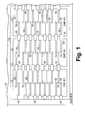
- FIG. 1shows a wafer 100 including a plurality of dice 101 , 102 , and 103 that are joined together along saw streets 105 .
- Wafer 100is illustrated as a square wafer but it will be understood that the wafer is not so limited and includes 200 millimeter, 300 millimeter, and 450 millimeter wafers known to those of skill in the art.
- wafer 100is illustrated with only three dice 101 , 102 , 103 thereon. It will be understood that the wafer 100 may have greater than two or three dice. In an embodiment, the wafer has greater than one thousand dice.
- a dieis an individual pattern, typically rectangular, on a substrate or wafer that contains circuitry, or integrated circuit devices, to perform a specific function.
- Each die 101 - 103includes an electrical circuit fabricated thereon according to known techniques.
- the die 101 - 103include integrated circuit elements such as capacitors, transistors, line, interconnects, plugs, pads, I/O connections, insulators, and/or other elements known in the art. These integrated circuit elements form electronic components such as processors and memory devices. Examples of memory devices include DRAM, SRAM, SDRAM, EEPROM, flash memory, ROM, etc.
- semiconductor wafer 100contains a repeated pattern of such dice containing the same functionality.
- Dice 101 - 103include bonding pads 106 .
- dice 101 - 103are identical and are formed by repeating a mask pattern on the wafer 100 .
- pads 106are at the top layer of the die.
- pads 106have a top surface aligned with the top surface of the thus-formed die.
- pads 106are aligned lengthwise along the middle of the die. Other embodiments of the invention are not limited to the pads 106 being positioned in the middle of the die.
- An electrically conductive line 108extends from each of the pads 106 to the periphery of the die 101 - 103 . Each line 108 electrically connects one pad 106 to one edge contact 109 .
- Edge contacts 109are positioned at the periphery of each die. Contacts 109 that are positioned at the periphery of two adjacent dice are integrally formed. That is, contacts 109 at the saw street 105 between die 101 and die 102 are connected to lines 108 of both die 101 and 102 . These contacts 109 are separated during a separation or dicing operation as described herein. Each of the pads 106 , lines 108 , and contacts 109 are not labeled in FIG. 1 for clarity. Each unit of connected pad 106 , line 108 , and contact 109 act as input/output connections to the internal circuits of the die. In an embodiment, the dice 101 - 103 are separated and further processed, e.g., tested or packaged, to form an end integrated circuit product.
- third metal redistribution wafer level packaging technologyis used on the wafer 100 to form the lines 108 from the bond pads 106 to the edge contacts 109 .
- Channelsare formed in the saw streets 105 .
- the wafer 100is first sawed about half to about three-quarter way through at the saw streets 105 . This forms the channels in the saw streets 105 between die 101 - 103 . Electrically conductive material is patterned in the channels to form the edge contacts 109 .
- Third metal redistribution on the wafer 100creates the lines 108 out from the bond pads 106 to the edge contacts 109 .
- lines 108 on the adjacent dice 101 , 102 or 102 , 103connect to the bond pads 106 of the adjacent die to a same edge contact as shown in FIG. 1 .
- the wafer 100is coated with polymide (PI), benzocyclobutenes (BCB) or other non-conductive materials except at the edge contacts.
- PIpolymide
- BCBbenzocyclobutenes
- Each individual dieis then singulated by sawing, breaking at the saw-streets or grinding or other dicing methods known in the art.
- the electrical connections of the die 101 , 102 , or 103 to external devicesare made through the edge contacts 109 .
- the singulated die 101 , 102 , or 103is mounted on a printed circuit board with the land patterns created to correspond to the locations of via-holes on the board.
- FIG. 2shows a die 201 including bonding pads 206 , electrically conductive lines 208 and contacts 209 .
- the pads 206are flush with the top surface 211 of the die 201 .
- the lines 208are flush with the top surface 211 of the die 201 .
- the top surface of the contacts 209are flush with the top surface 211 of the die 201 .
- the top surface of the contacts 209are beneath the top surface 211 of the die 201 .
- the contacts 209extend outwardly from the side surface 212 of the die 201 .
- contacts 209are metal.
- contacts 209include tungsten.
- contacts 209include titanium.
- the contacts 209include a noble metal. In an embodiment, the contacts 209 include gold. In an embodiment, contacts 209 include a gold coating on another metal or metal alloy. In an embodiment, the contacts 209 include silver. In an embodiment, contacts 209 include a silver coating on another metal or metal alloy.
- the gold or silver coatings on contacts 209are provided to improve the electrical connection between the contacts and external devices in which the die or chip 209 will be placed. In another embodiment, the chip 209 is enclosed, except for at least a portion of the contacts 209 , by an encapsulant. Encapsulants are known to those of ordinary skill in the art of integrated circuit packaging.
- FIG. 3Ashows a partial view of a wafer 300 , which has undergone fabrication processing steps to form the desired integrated circuits on each die 301 , 302 .
- the fabrication stepsinclude masking, depositing, etching, and other steps as understood in the art.
- a recess 315is formed in the saw street 305 .
- a recess 315is formed in each saw street 305 .
- a recess 315is formed in each saw street 305 along the longitudinal (longest) length of a rectangular die.
- the recess 315is formed on other sides of the die.
- recessesare formed on all four sides of the die.
- recess 315extends downwardly from the top surface 311 of wafer 300 about half the height of the wafer or die.
- the recess 315in an embodiment, is formed while forming integrated circuit structures in the dice.
- recess 315is etched into the wafer 300 after the circuits are formed in each die 301 , 302 .
- the recess 315extends the entire length of the saw street 305 . Bond pads 306 are formed on the dice 301 , 302 according to conventional processes.
- the wafer top surface 311is masked leaving open the area of the metal lines from bond pads 306 of one die 301 to bond pads 306 of the adjacent die 302 . It is within the scope of the various embodiments to use positive or negative resist mask.
- the maskin an embodiment, leaves open a wider area adjacent the saw street 305 on the dice 301 , 302 and in the recess 315 .
- the electrically conductive material for the lines 308 and the edge contacts 309is deposited on the wafer 300 . The material forms the lines 308 and edge contacts 309 in the open areas of the mask.
- the recesses 315are formed according to various embodiments of the invention.
- the wafer 300e.g., dice 301 , 302 and saw street 305 , is masked leaving openings aligned with the location of the edge contact 309 .
- Edge contact materialsuch as metal, is deposited in the opening to form the edge contact 309 .
- the mask and edge contact material on the maskis removed from the wafer 300 .
- the lines 308are formed to connect the edge contact to at least one of the bond pads 306 of the adjacent dice 301 , 302 .
- passivation layer 320is deposited according to conventional techniques. Passivation layer 320 covers the entire wafer except over the edge contacts 309 . In an embodiment, passivation layer 320 does not cover the saw street 305 . In an embodiment, passivation layer 320 includes inorganic polymers. In an embodiment, passivation layer 320 includes benzocyclobutenes (BCB). In an embodiment, passivation layer 320 includes polymides (PI). In an embodiment, passivation layer 320 includes at least one of silicon dioxide, silicon nitride, or silicon oxynitride. In an embodiment, passivation layer 320 includes organic polymers.
- a cutter 325is aligned with the saw street 305 , and, in particular, with edge contact 309 ( FIG. 3B ).
- Cutter 325cuts a center portion of the contact 309 to create edge contacts 309 1 and 309 2 .
- Edge contact 309 1is on the peripheral edge surface of the first die 301 .
- Edge contact 309 2is on the peripheral edge surface of the second die 302 .
- cutter 325only cuts the contact 309 , thus creating a scribe in the wafer 300 along saw street 305 .
- Adjacent wafers 301 , 302can be separated along the scribe by using a scribe and break technique. Referring to FIG. 3C , the cutter 326 completely cuts through the wafer 300 along the saw street 305 .
- At least one of cutters 325 , 326is a saw. In an embodiment, both of cutters 325 , 326 are saws. In an embodiment, at least one of cutters 325 , 326 is a laser.
- each die 301 , 302includes edge contacts 309 1 , 309 2 at peripheral surfaces of the die. Accordingly, the dice 301 , 302 have a height equal to the die or wafer height and the edge contacts 309 do not add to the height of the separated dice.
- eachis individually packaged in an encapsulant 340 .
- the encapsulant 340surrounds the dice 301 , 302 except for at least part of the edge contacts 309 .
- the encapsulant 340protects the dice 301 , 302 from an operating environment while the edge contacts 309 provide input and output signals to the circuits internal to the packaged die 301 , 302 .
- FIGS. 4A , 4 B, and 4 Care cross sectional views of two dice 401 , 402 according to an embodiment of the invention.
- Wafer 400includes a plurality of dice 401 , 402 .
- Each die 401 , 402includes circuits, such as integrated circuits, fabricated according to conventional processes. The circuits require communication to external circuits such as a buss, mother boards, and other electronic devices. Consequently, each die 401 , 402 includes a bond pad 406 .
- Wafer 400further includes saw streets 405 dividing the dice 401 , 402 whereat the dice are separated. A recess 415 is formed in the saw street 405 that is intermediate the dice 401 , 402 .
- a mask layer 431is formed over the wafer 400 except where the edge contact 409 is to be positioned.
- the mask layer 431is formed according to techniques known to one of skill in the art.
- the electrically conductive material of the edge contact 409is deposited into the recess.
- the conductive material of edge contact 409in an embodiment, is sputtered onto the wafer.
- the conductive material of the edge contact 409is deposited by chemical vapor deposition.
- the conductive material of the edge contact 409is deposited by evaporation sources.
- the conductive material of the edge contact 409is deposited by electron gun evaporation.
- the edge contacts 409are formed after lines 408 are formed.
- a second masking layer 432is formed over the wafer 400 .
- Masking layer 432extends a distance over the sides of the contact 409 .
- the width of the extension of the masking layer 432 over the contact 409is essentially equal to the width of the finished edge contacts 409 1 and 409 2 on the respective dice 401 and 402 .
- the unitary contact 409is etched away where it is not covered by masking layer 432 .
- contact 409is etched down to the portion of the wafer 400 beneath the recess.
- contact 409is etched so that it has a U-shape.
- the masking layers 431 , 432are removed ( FIG. 4B ).
- the dice 401 and 402are then separated or diced ( FIG. 4C ).
- the individual dice 401 and 402are then packaged, e.g., for example coated with a encapsulant, except for at least part of the edge contacts 409 .
- FIG. 5shows an embodiment which includes the wafer 500 being diced into a plurality of dice 501 , 502 .
- Each die 510 , 502includes bond pads 506 and electrical signal carrying lines 508 .
- the edge contacts 509are connected to the lines 508 .
- the edge contacts 509are formed according to various embodiments.
- the edge contacts 509extend to the top surface of the passivation layer 520 . That is, the top surface of the edge contact 509 is essentially in the same plane as the top surface of the passivation layer.
- the edge contacts 509have a top surface that is essentially in the same plane as a top surface of the encapsulant encasing the die 501 .
- the edge contacts 509have a bottom surface that is essentially in the same plane as a bottom surface of the encapsulant encasing the die 501 . In an embodiment, the edge contacts 509 have a height greater than one-half the height of the peripheral edge surface of the die. In an embodiment, the edge contacts 509 extend along approximately 75% of the height of the peripheral surface of the die.
- FIG. 6shows top view of a singulated land grid array, and a packaged die 601 .
- Each of the edge contacts 609are in electrical and physical contact with a contact pad 645 .
- the contact pads 645extend under the main body of the packaged die 601 . In an embodiment, contact pads 645 extend outward of the main body of the packaged die 601 .
- Contact pads 645act as contacts between the circuits external to the packaged die 601 and the die 601 through edge contacts 609 , lines 608 and bond pads 606 . Only one set of lines 608 and bond pads 606 are shown in FIG. 6 for sake of clarity. It will be understood that each of the edge contacts 609 may be connected to a line 608 , which in turn is connected to a bonding pad 606 .
- FIG. 6further illustrates line 608 and pad 609 in broken line as they are covered by an encapsulation layer that surrounds the die per se and protects the internal circuits from the environment, e.g., dirt, debris, moisture and
- An electrical device 650includes a socket, slot, recess or the like 652 which includes device contacts 653 .
- the packaged die 601is adapted to be received in the socket 652 , wherein the contact pads 645 engage contacts 653 .
- the contacts 653are electrically connect with communication lines connected to external circuits of the electrical device 650 .
- Electrical device 650includes mother boards, computers, consumer electronics, printed circuit boards, and the like.
- the contact pads 645in an embodiment, press fit against the device contacts 653 to hold the die 601 in the socket 652 .
- the edge contacts 609directly contact device contacts 653 .
- An embodiment of the inventionincludes fixing contact pads 645 to a substrate (not shown).
- the substrateis fixed to the bottom of the die.
- Encapsulant and substrateencase the die to protect it from the environment.
- Contact pads 645 and edge contacts 609are electrically conductive.
- pads 645 and contacts 609are made of a metal.
- at least one of contacts 609 and pads 645include a metal alloy.
- pads 645include copper.
- pads 645include a noble metal.
- pads 645include gold.
- pads 645include silver.
- the encapsulantin an embodiment, encases the die without a substrate.
- circuit module 700may be a combination of dice 701 representing a variety of functions, or a combination of dice 701 containing the same functionality.
- circuit module 700includes at least one socket, slot, recess or the like 752 into which the die 701 is received.
- One or more dice 701 of circuit module 700include I/O structures in accordance with various embodiments of the invention and/or are fabricated in accordance with various embodiments of the invention.
- dice 701are inserted into a slot 752 in a circuit board 750 such that the contacts 209 , 309 , 509 , or 609 are in electrical communication with the contacts in the slot 752 .
- contacts 209 , 309 , 509 , or 609are in physical contact with contacts in the slot 752 .
- the contacts 209 , 309 , 509 , or 609are press fit into the slot 752 against the contacts of the slot.
- circuit module 700is a printed circuit board having land patterns on which solder paste is applied, e.g., by printing the solder paste.
- a die 701is picked and placed at the mount with the die contacts 209 , 309 , 509 , or 609 aligned with the paste covered contacts of the mount. Either the die contacts or the mount contacts are reflowed to create a physical and electrical connection.
- circuit module 700Some examples of a circuit module include memory modules, device drivers, power modules, communication modems, processor modules and application-specific modules, and may include multilayer, multichip modules. Such modules will have a chip receiver in which a chip is inserted.
- Circuit module 700may be a subcomponent of a variety of electronic systems, such as a clock, a television, a cell phone, a personal computer, an automobile, an industrial control system, an aircraft and others. Such modules will have a circuit module receiver in which a circuit module is inserted.
- Circuit module 700will have a variety of leads 705 1 through 705 N extending therefrom and coupled to the contacts 209 , 309 , 409 , or 509 of dice 701 providing unilateral or bilateral communication and control.
- FIG. 8shows one embodiment of a circuit module as memory module 800 .
- Memory module 800contains multiple memory devices 801 contained on support 861 .
- support 861includes slots 852 for receiving memory devices 801 as described herein. The number of memory devices generally depends upon the desired bus width and the desire for parity.
- Memory devices 801may include one or more dice in accordance with various embodiments of the invention.
- the support 861includes sockets, slots, recesses or the like 852 , each adapted to receive a memory device 801 and provide electrical communication between a bus and memory device 801 .
- Memory module 800accepts a command signal from an external controller (not shown) on a command link 863 and provides for data input and data output on data links 865 .
- the command link 863 and data links 865are connected to leads 867 extending from the support 815 . Leads 867 are shown for conceptual purposes and are not limited to the positions shown in FIG. 8 .
- FIG. 9shows one embodiment of an electronic system 900 containing one or more circuit modules 700 . At least one of the circuit modules 700 contains a die in accordance with various embodiments of the invention.
- Electronic system 900generally contains a user interface 969 .
- User interface 969provides a user of the electronic system 900 with some form of control or observation of the results of the electronic system 900 .
- Some examples of user interface 969include the keyboard, pointing device, monitor or printer of a personal computer; the tuning dial, display or speakers of a radio; the ignition switch, gauges or gas pedal of an automobile; and the card reader, keypad, display or currency dispenser of an automated teller machine.
- User interface 969may further describe access ports provided to electronic system 900 .
- Access portsare used to connect an electronic system to the more tangible user interface components previously exemplified.
- One or more of the circuit modules 700may be a processor providing some form of manipulation, control or direction of inputs from or outputs to user interface 969 , or of other information either preprogrammed into, or otherwise provided to, electronic system 900 .
- electronic system 900includes memory modules 800 .
- electronic system 900will often be associated with certain mechanical components (not shown) in addition to circuit modules 700 and user interface 969 . It will be appreciated that the one or more circuit modules 700 in electronic system 900 can be replaced by a single integrated circuit.
- electronic system 900may be a subcomponent of a larger electronic system.
- FIG. 10shows one embodiment of an electronic system as memory system 1000 .
- Memory system 1000contains one or more memory modules 800 and a memory controller 1070 . At least one of the memory modules 800 includes a die in accordance with various embodiments of the invention.
- Memory controller 1070provides and controls a bidirectional interface between memory system 1000 and an external system bus 1072 .
- Memory system 1000accepts a command signal from the external bus 1072 and relays it to the one or more memory modules 800 on a command link 1074 .
- Memory system 1000provides for data input and data output between the one or more memory modules 800 and external system bus 1072 on data links 1076 .
- FIG. 11shows a further embodiment of an electronic system as a computer system 1100 .
- Computer system 1100contains a processor 1101 and a memory system 1000 housed in a computer unit 1180 .
- the memory system 1000includes a die in accordance with various embodiments of the invention.
- processor 1101includes a die in accordance with various embodiments of the invention.
- Computer system 1100is but one example of an electronic system containing another electronic system, i.e., memory system 1000 , as a subcomponent.
- Computer system 1100optionally contains user interface components. Depicted in FIG.
- a keyboard 1181a pointing device 1183 such as a mouse, trackball, or joystick
- a monitor 1185a printer 1187 and a bulk storage device 1189 .
- other componentsare often associated with computer system 1100 such as modems, device driver cards, additional storage devices, etc. These other components, in an embodiment, include a die in accordance with various embodiments of the invention.
- the processor 1101 and memory system 1000 of computer system 1100can be incorporated on a single integrated circuit. Such single package processing units reduce the communication time between the processor and the memory circuit.
- Some embodiments of the inventionprovide methods for producing a packaged die.
- the cuttercuts along the saw street but does not cut all the way through the wafer. Thus, channels intermediate the dice are created. Edge contact material is deposited or patterned in the channels. The dice are diced. The dice will have edge contacts around the periphery of the die. Thus, the contacts do not add to the height of the die and/or package. Accordingly, some embodiments of the invention provide an extremely low profile package, i.e., the package thickness is essentially the same as the die thickness. Shorter length contacts may further provide superior signal integrity along with space savings.
Landscapes
- Engineering & Computer Science (AREA)
- Computer Hardware Design (AREA)
- Microelectronics & Electronic Packaging (AREA)
- Power Engineering (AREA)
- Manufacturing & Machinery (AREA)
- Physics & Mathematics (AREA)
- Condensed Matter Physics & Semiconductors (AREA)
- General Physics & Mathematics (AREA)
- Semiconductor Integrated Circuits (AREA)
- Perforating, Stamping-Out Or Severing By Means Other Than Cutting (AREA)
Abstract
Description
This application is Continuation of U.S. application Ser. No. 11/934,556 filed Nov. 2, 2007 now U.S. Pat. No. 7,675,169 which is a is a Divisional of U.S. application Ser. No. 11/281,084 filed Nov. 17, 2005 now U.S. Pat. No. 7,358,154, which is a Divisional of U.S. application Ser. No. 10/929,932, filed Aug. 30, 2004, which is a Divisional of U.S. application Ser. No. 10/118,576, filed Apr. 8, 2002, now U.S. Pat. No. 6,894,386, which claims priority under 35 U.S.C. 119 from Singapore Application No. 200106182-9 filed Oct. 8, 2001, all of which are incorporated herein by reference in their entirety.
Wafers are fabricated with a plurality of dice each having a plurality of integrated circuit elements therein. A die represents one individual chip that must be separated from adjacent dice before packaging. Contacts are added to the die before packaging. One type of contact is a solder ball. Wafer level packaging (WLP) refers to the complete packaging of an electronic component at the die or the wafer level. WLP is normally considered as a true chip size package. However, the profile of most WLP is the sum of the thickness of the die and the solder balls. It is desired to reduce the profile and/or thickness of packaged components.
For the reasons stated above, for other reasons stated below, and for other reasons which will become apparent to those skilled in the art upon reading and understanding the present specification, there is a need in the art for an improved electronic component package and methods of packaging electronic components.
Some embodiments of the invention are directed to integrated circuit dice and their method of manufacture. An embodiment of the invention includes an edge contact at a peripheral surface of the die. The edge contact connects to a bond pad through a line. In an embodiment, adjacent dice on a wafer are connected to a same edge contact. The edge contact is divided. In an embodiment, the edge contact is divided when the dice are separated. In an embodiment, the edge contact is in the saw street and is divided when the wafer is diced. The die, in some embodiments, includes a main body including a top layer, a bottom layer, and a peripheral edge surface extending between the top layer and the bottom layer. The main body includes an integrated circuit therein that is electrically connected to the bond pad. In an embodiment, the edge contact is beneath the top layer. In an embodiment, the edge contact is above the bottom layer such that the edge contact does not increase the height of the die. In an embodiment, the bond pad is at the top layer. In an embodiment, the die is encased by an encapsulant.
Some embodiments of the invention include methods for creating a die. An embodiment of the invention includes fabricating at least two dice on a wafer, wherein the at least two dice are joined at an electrically conductive element in a saw street, and separating the at least two dice from each other along the saw street. At least part of the electrically conductive element remains with each die. In an embodiment, the electrically conductive element is created by forming a recess in the saw street and filling the recess with an electrically conducting material. In an embodiment of the invention, the method includes connecting a bond pad from at least one of the dice to the electrically conductive material. An embodiment of the invention includes fabricating circuits for a memory device in at least one of the dice. In an embodiment of the invention, forming the recess includes sawing along the saw street to a depth of about half a height of the die. An embodiment of the invention includes connecting the bond pad includes depositing a metal on the wafer between the bond pad and the electrically conductive material.
A further embodiment of the method includes patterning a recess in a saw street intermediate adjacent dice in a wafer, depositing an electrically conductive material in the recess to form an edge contact, connecting a bond pad of both dice to the edge contact, and separating the adjacent dice along the saw street such that each dice includes a part of the edge contact. An embodiment of the invention includes masking the wafer such that the electrically conductive material is deposited only in the recess.
Embodiments of the invention also include substrates, wafers, integrated circuit packages, electrical devices, memory units, memory modules, electrical systems, computers, which include at least one die.
These and other embodiments, aspects, advantages, and features of the invention will be set forth in part in the description which follows, and in part will become apparent to those skilled in the art by reference to the following description of the invention and referenced drawings or by practice of the invention.
In the following detailed description of various embodiments, reference is made to the accompanying drawings which form a part hereof, and in which is shown by way of illustration specific embodiments in which the inventions may be practiced. These embodiments are described in sufficient detail to enable those skilled in the art to practice the invention, and it is to be understood that other embodiments may be utilized and that process, electrical or mechanical changes may be made. The terms wafer and substrate used in the following description include any base semiconductor structure. Both are to be understood as including silicon-on-sapphire (SOS) technology, silicon-on-insulator (SOI) technology, thin film transistor (TFT) technology, doped and undoped semiconductors, epitaxial layers of a silicon supported by a base semiconductor structure, as well as other semiconductor structures well known to one skilled in the art. The following detailed description is, therefore, not to be taken in a limiting sense, and the scope of the various embodiments is defined only by the appended claims and their equivalents.
The present description uses a reference number convention of the first digit corresponding to the figure in which the number references and the last two digits corresponding to like elements throughout the description. For example, the edge contact has a reference number of X09, where X is the number of figure on which the reference number first appears.
Dice101-103 includebonding pads 106. In an embodiment, dice101-103 are identical and are formed by repeating a mask pattern on thewafer 100. In an embodiment,pads 106 are at the top layer of the die. In an embodiment,pads 106 have a top surface aligned with the top surface of the thus-formed die. In an embodiment,pads 106 are aligned lengthwise along the middle of the die. Other embodiments of the invention are not limited to thepads 106 being positioned in the middle of the die. An electricallyconductive line 108 extends from each of thepads 106 to the periphery of the die101-103. Eachline 108 electrically connects onepad 106 to oneedge contact 109.Edge contacts 109 are positioned at the periphery of each die.Contacts 109 that are positioned at the periphery of two adjacent dice are integrally formed. That is,contacts 109 at thesaw street 105 betweendie 101 and die102 are connected tolines 108 of both die101 and102. Thesecontacts 109 are separated during a separation or dicing operation as described herein. Each of thepads 106,lines 108, andcontacts 109 are not labeled inFIG. 1 for clarity. Each unit ofconnected pad 106,line 108, and contact109 act as input/output connections to the internal circuits of the die. In an embodiment, the dice101-103 are separated and further processed, e.g., tested or packaged, to form an end integrated circuit product.
In an embodiment, third metal redistribution wafer level packaging technology is used on thewafer 100 to form thelines 108 from thebond pads 106 to theedge contacts 109. Channels are formed in thesaw streets 105. In an embodiment, thewafer 100 is first sawed about half to about three-quarter way through at thesaw streets 105. This forms the channels in thesaw streets 105 between die101-103. Electrically conductive material is patterned in the channels to form theedge contacts 109. Third metal redistribution on thewafer 100 creates thelines 108 out from thebond pads 106 to theedge contacts 109. In an embodiment,lines 108 on theadjacent dice bond pads 106 of the adjacent die to a same edge contact as shown inFIG. 1 . In an embodiment, thewafer 100 is coated with polymide (PI), benzocyclobutenes (BCB) or other non-conductive materials except at the edge contacts. Each individual die is then singulated by sawing, breaking at the saw-streets or grinding or other dicing methods known in the art. The electrical connections of thedie edge contacts 109. In an embodiment, the singulated die101,102, or103 is mounted on a printed circuit board with the land patterns created to correspond to the locations of via-holes on the board.
An embodiment for fabricating the die will now be described with reference toFIGS. 3A-3D .FIG. 3A shows a partial view of awafer 300, which has undergone fabrication processing steps to form the desired integrated circuits on each die301,302. The fabrication steps include masking, depositing, etching, and other steps as understood in the art. In thesaw street 305, arecess 315 is formed. In an embodiment, arecess 315 is formed in each sawstreet 305. In an embodiment, arecess 315 is formed in each sawstreet 305 along the longitudinal (longest) length of a rectangular die. In an embodiment, therecess 315 is formed on other sides of the die. For example, on a rectangular or square die, recesses are formed on all four sides of the die. In an embodiment,recess 315 extends downwardly from thetop surface 311 ofwafer 300 about half the height of the wafer or die. Therecess 315, in an embodiment, is formed while forming integrated circuit structures in the dice. In an embodiment,recess 315 is etched into thewafer 300 after the circuits are formed in each die301,302. In an embodiment, therecess 315 extends the entire length of thesaw street 305.Bond pads 306 are formed on thedice bond pads 306 are formed, thewafer top surface 311 is masked leaving open the area of the metal lines frombond pads 306 of one die301 tobond pads 306 of theadjacent die 302. It is within the scope of the various embodiments to use positive or negative resist mask. The mask, in an embodiment, leaves open a wider area adjacent thesaw street 305 on thedice recess 315. The electrically conductive material for thelines 308 and theedge contacts 309 is deposited on thewafer 300. The material forms thelines 308 andedge contacts 309 in the open areas of the mask.
Therecesses 315 are formed according to various embodiments of the invention. Thewafer 300, e.g.,dice street 305, is masked leaving openings aligned with the location of theedge contact 309. Edge contact material, such as metal, is deposited in the opening to form theedge contact 309. In an embodiment, the mask and edge contact material on the mask is removed from thewafer 300. In an embodiment, thelines 308 are formed to connect the edge contact to at least one of thebond pads 306 of theadjacent dice
After the formation of thelines 308 of each die301,302, which lines are connected atedge contacts 309, thewafer 300 receives apassivation layer 320. In an embodiment,passivation layer 320 is deposited according to conventional techniques.Passivation layer 320 covers the entire wafer except over theedge contacts 309. In an embodiment,passivation layer 320 does not cover thesaw street 305. In an embodiment,passivation layer 320 includes inorganic polymers. In an embodiment,passivation layer 320 includes benzocyclobutenes (BCB). In an embodiment,passivation layer 320 includes polymides (PI). In an embodiment,passivation layer 320 includes at least one of silicon dioxide, silicon nitride, or silicon oxynitride. In an embodiment,passivation layer 320 includes organic polymers.
Acutter 325 is aligned with thesaw street 305, and, in particular, with edge contact309 (FIG. 3B ).Cutter 325 cuts a center portion of thecontact 309 to createedge contacts Edge contact 3091is on the peripheral edge surface of thefirst die 301.Edge contact 3092is on the peripheral edge surface of thesecond die 302. In an embodiment,cutter 325 only cuts thecontact 309, thus creating a scribe in thewafer 300 alongsaw street 305.Adjacent wafers FIG. 3C , thecutter 326 completely cuts through thewafer 300 along thesaw street 305. In an embodiment, at least one ofcutters cutters cutters dice edge contacts dice edge contacts 309 do not add to the height of the separated dice.
Once thedice encapsulant 340. Theencapsulant 340 surrounds thedice edge contacts 309. Thus, theencapsulant 340 protects thedice edge contacts 309 provide input and output signals to the circuits internal to the packageddie
After formation of theunitary edge contact 409 in the form of a solid plug of electrically conductive material in thesaw street recess 415, asecond masking layer 432 is formed over thewafer 400. Maskinglayer 432 extends a distance over the sides of thecontact 409. The width of the extension of themasking layer 432 over thecontact 409 is essentially equal to the width of thefinished edge contacts respective dice unitary contact 409 is etched away where it is not covered by maskinglayer 432. In an embodiment, contact409 is etched down to the portion of thewafer 400 beneath the recess. In an embodiment, contact409 is etched so that it has a U-shape. Thereafter, the masking layers431,432 are removed (FIG. 4B ). Thedice FIG. 4C ). Theindividual dice edge contacts 409.
Anelectrical device 650 includes a socket, slot, recess or the like652 which includesdevice contacts 653. The packaged die601 is adapted to be received in thesocket 652, wherein thecontact pads 645 engagecontacts 653. Thecontacts 653 are electrically connect with communication lines connected to external circuits of theelectrical device 650.Electrical device 650 includes mother boards, computers, consumer electronics, printed circuit boards, and the like. Thecontact pads 645, in an embodiment, press fit against thedevice contacts 653 to hold thedie 601 in thesocket 652. In an embodiment, theedge contacts 609 directly contactdevice contacts 653.
An embodiment of the invention includes fixingcontact pads 645 to a substrate (not shown). The substrate is fixed to the bottom of the die. Encapsulant and substrate encase the die to protect it from the environment. Contactpads 645 andedge contacts 609 are electrically conductive. In an embodiment,pads 645 andcontacts 609 are made of a metal. In an embodiment, at least one ofcontacts 609 andpads 645 include a metal alloy. In an embodiment,pads 645 include copper. In an embodiment,pads 645 include a noble metal. In an embodiment,pads 645 include gold. In an embodiment,pads 645 include silver. The encapsulant, in an embodiment, encases the die without a substrate.
Circuit Modules
As shown inFIG. 7 , two ormore dice 701 may be combined, with or without protective casing, into acircuit module 700 to enhance or extend the functionality of anindividual die 701.Circuit module 700 may be a combination ofdice 701 representing a variety of functions, or a combination ofdice 701 containing the same functionality. In an embodiment,circuit module 700 includes at least one socket, slot, recess or the like752 into which thedie 701 is received. One ormore dice 701 ofcircuit module 700 include I/O structures in accordance with various embodiments of the invention and/or are fabricated in accordance with various embodiments of the invention. In an embodiment,dice 701 are inserted into aslot 752 in acircuit board 750 such that thecontacts slot 752. In an embodiment,contacts slot 752. In an embodiment, thecontacts slot 752 against the contacts of the slot.
Some examples of a circuit module include memory modules, device drivers, power modules, communication modems, processor modules and application-specific modules, and may include multilayer, multichip modules. Such modules will have a chip receiver in which a chip is inserted.Circuit module 700 may be a subcomponent of a variety of electronic systems, such as a clock, a television, a cell phone, a personal computer, an automobile, an industrial control system, an aircraft and others. Such modules will have a circuit module receiver in which a circuit module is inserted.Circuit module 700 will have a variety ofleads 7051through705Nextending therefrom and coupled to thecontacts dice 701 providing unilateral or bilateral communication and control.
Electronic Systems
It is desired to reduce the size of packaged components. This results in packaging material savings and increases throughput by reducing packaging times. Moreover, with the growing popularity of smaller electronic device the electronic components must be as small as possible. Some embodiments of the invention provide methods for producing a packaged die. In an embodiment, the cutter cuts along the saw street but does not cut all the way through the wafer. Thus, channels intermediate the dice are created. Edge contact material is deposited or patterned in the channels. The dice are diced. The dice will have edge contacts around the periphery of the die. Thus, the contacts do not add to the height of the die and/or package. Accordingly, some embodiments of the invention provide an extremely low profile package, i.e., the package thickness is essentially the same as the die thickness. Shorter length contacts may further provide superior signal integrity along with space savings.
Although specific embodiments have been illustrated and described herein, it will be appreciated by those of ordinary skill in the art that any arrangement which is calculated to achieve the same purpose may be substituted for the specific embodiments shown. Many adaptations of the invention will be apparent to those of ordinary skill in the art. For example, other integrated circuit processing equipment may be utilized in conjunction with various embodiments of the invention. For another example, other integrated circuit fabrication processes are adapted to produce the dice and chips according to some embodiments of the invention. It is manifestly intended that the various embodiments of this invention be limited only by the following claims and equivalents thereof.
Claims (20)
1. An apparatus comprising an integrated circuit die, the integrated circuit die including:
a main body including a top layer, a bottom layer, and a peripheral edge surface extending between the top layer and the bottom layer;
a bond pad on the main body;
an edge contact at the peripheral edge surface, wherein the edge contact includes a bottom surface that is substantially in the same plane as a surface of an encapsulant encasing the die; and
a line connecting the bond pad to the edge contact.
2. The apparatus ofclaim 1 , wherein the edge contact includes a top surface and an edge surface, and wherein the top, bottom, and edge surfaces of the edge contact form a circumferential edge contact.
3. The apparatus ofclaim 2 , wherein the edge contact has an outer peripheral surface that is substantially coplanar with the peripheral edge surface of the main body.
4. The apparatus ofclaim 1 , wherein the edge contact is configured to make electrical contact with a contact pad extending under the main body.
5. The apparatus ofclaim 4 , wherein the edge contact includes a top surface and an edge surface, and wherein the edge contact and the contact pad form a “C” shape at the peripheral edge surface.
6. An apparatus comprising a grid array packaged die, comprising:
an integrated circuit die comprising:
a main body including a top layer, a bottom layer, and a peripheral surface extending between the top layer and the bottom layer;
a bond pad on one of: the top layer and the bottom layer of the main body;
an edge contact at the peripheral edge surface, wherein the edge contact includes a bottom surface that is substantially in the same plane as a surface of an encapsulant at least partially encasing the die; and
a line connecting the bond pad to the edge contact; and
a contact pad on the other of: the top layer and the bottom layer of the main body, wherein the contact pad is not formed on the same layer of the main body on which the bond pad is formed, the contact pad communicatively coupled to the edge contact.
7. The apparatus ofclaim 6 , wherein the edge contact includes a top surface and an edge surface, and wherein the edge contact and the contact pad form a “C” shape at the peripheral edge surface.
8. The apparatus ofclaim 6 , including a substrate, wherein the contact pad is fixed to the substrate.
9. The apparatus ofclaim 8 , wherein the encapsulant at least partially encases the integrated circuit die and the substrate.
10. The apparatus ofclaim 8 , wherein the substrate is configured to be received in a socket.
11. The apparatus ofclaim 6 , including a capacitive circuit element communicatively coupled to the bond pad.
12. An apparatus comprising a grid array packaged die, comprising:
an integrated circuit die comprising:
a main body including a top layer, a bottom layer, and a peripheral surface extending between the top layer and the bottom layer;
a bond pad on one of: the top layer and the bottom layer of the main body;
an edge contact embedded in the peripheral edge surface; and
a redistribution line on the bond pad layer connecting the bond pad to the edge contact; and
a contact pad on the other of: the top layer and the bottom layer of the main body, wherein the contact pad is formed on a different layer of the main body than the bond pad, the contact pad communicatively coupled to the edge contact.
13. The apparatus ofclaim 12 , including an encapsulant at least partially encasing the die,
wherein the edge contact includes a bottom surface that is substantially in the same plane as a bottom surface of the encapsulant and a top surface that is substantially in the same plane as a top surface of the encapsulant.
14. The apparatus ofclaim 12 , including an encapsulant encasing the die, wherein the edge contact includes a top surface, and wherein the edge contact forms a circumferential edge contact at the peripheral edge surface.
15. The apparatus ofclaim 14 , wherein the edge contact and the contact pad form a “C” shaped contact.
16. The apparatus ofclaim 12 , wherein the contact pad is fixed to a substrate and is configured for surface mounting to a conductive line of a circuit board.
17. A wafer, comprising:
a plurality of integrated circuit dice, wherein each integrated circuit die includes a bond pad;
saw streets between adjacent pairs of the plurality of dice;
an edge contact recessed in a saw street between an adjacent pair of the integrated circuit dice, wherein the edge contact does not extend above top surfaces of the pair of adjacent dice;
a first electrically conductive line extending from a bond pad of a first die of the pair of dice to the edge contact;
a second electrically conductive line extending from a bond pad of a second die of the pair of dice to the edge contact; and
a passivation layer covering a portion of the wafer excluding the edge contact.
18. The wafer ofclaim 17 , wherein at least one of the integrated circuit dice includes a capacitive circuit element.
19. The wafer ofclaim 17 , wherein a bond pad is on a top surface of at least one of the integrated circuit dice and the edge contact is at a peripheral surface of the at least one of the integrated circuit dice.
20. The wafer ofclaim 17 , wherein the first die and the second die have substantially coplanar top surfaces and substantially coplanar bottom surfaces, and wherein the edge contact does not extend below the bottom surfaces.
Priority Applications (1)
| Application Number | Priority Date | Filing Date | Title |
|---|---|---|---|
| US12/705,277US8115306B2 (en) | 2001-10-08 | 2010-02-12 | Apparatus and method for packaging circuits |
Applications Claiming Priority (7)
| Application Number | Priority Date | Filing Date | Title |
|---|---|---|---|
| SG200106182-9 | 2001-10-08 | ||
| SG200106182ASG102639A1 (en) | 2001-10-08 | 2001-10-08 | Apparatus and method for packing circuits |
| US10/118,576US6894386B2 (en) | 2001-10-08 | 2002-04-08 | Apparatus and method for packaging circuits |
| US10/929,932US8138617B2 (en) | 2001-10-08 | 2004-08-30 | Apparatus and method for packaging circuits |
| US11/281,084US7358154B2 (en) | 2001-10-08 | 2005-11-17 | Method for fabricating packaged die |
| US11/934,556US7675169B2 (en) | 2001-10-08 | 2007-11-02 | Apparatus and method for packaging circuits |
| US12/705,277US8115306B2 (en) | 2001-10-08 | 2010-02-12 | Apparatus and method for packaging circuits |
Related Parent Applications (1)
| Application Number | Title | Priority Date | Filing Date |
|---|---|---|---|
| US11/934,556ContinuationUS7675169B2 (en) | 2001-10-08 | 2007-11-02 | Apparatus and method for packaging circuits |
Publications (2)
| Publication Number | Publication Date |
|---|---|
| US20100140794A1 US20100140794A1 (en) | 2010-06-10 |
| US8115306B2true US8115306B2 (en) | 2012-02-14 |
Family
ID=29212568
Family Applications (5)
| Application Number | Title | Priority Date | Filing Date |
|---|---|---|---|
| US10/118,576Expired - Fee RelatedUS6894386B2 (en) | 2001-10-08 | 2002-04-08 | Apparatus and method for packaging circuits |
| US10/929,932Expired - Fee RelatedUS8138617B2 (en) | 2001-10-08 | 2004-08-30 | Apparatus and method for packaging circuits |
| US11/281,084Expired - Fee RelatedUS7358154B2 (en) | 2001-10-08 | 2005-11-17 | Method for fabricating packaged die |
| US11/934,556Expired - Fee RelatedUS7675169B2 (en) | 2001-10-08 | 2007-11-02 | Apparatus and method for packaging circuits |
| US12/705,277Expired - Fee RelatedUS8115306B2 (en) | 2001-10-08 | 2010-02-12 | Apparatus and method for packaging circuits |
Family Applications Before (4)
| Application Number | Title | Priority Date | Filing Date |
|---|---|---|---|
| US10/118,576Expired - Fee RelatedUS6894386B2 (en) | 2001-10-08 | 2002-04-08 | Apparatus and method for packaging circuits |
| US10/929,932Expired - Fee RelatedUS8138617B2 (en) | 2001-10-08 | 2004-08-30 | Apparatus and method for packaging circuits |
| US11/281,084Expired - Fee RelatedUS7358154B2 (en) | 2001-10-08 | 2005-11-17 | Method for fabricating packaged die |
| US11/934,556Expired - Fee RelatedUS7675169B2 (en) | 2001-10-08 | 2007-11-02 | Apparatus and method for packaging circuits |
Country Status (2)
| Country | Link |
|---|---|
| US (5) | US6894386B2 (en) |
| SG (1) | SG102639A1 (en) |
Cited By (1)
| Publication number | Priority date | Publication date | Assignee | Title |
|---|---|---|---|---|
| US9536831B2 (en)* | 2015-05-12 | 2017-01-03 | United Microelectronics Corp. | Semiconductor device and method for fabricating the same |
Families Citing this family (71)
| Publication number | Priority date | Publication date | Assignee | Title |
|---|---|---|---|---|
| SG102639A1 (en)* | 2001-10-08 | 2004-03-26 | Micron Technology Inc | Apparatus and method for packing circuits |
| TWI232560B (en)* | 2002-04-23 | 2005-05-11 | Sanyo Electric Co | Semiconductor device and its manufacture |
| US7579681B2 (en)* | 2002-06-11 | 2009-08-25 | Micron Technology, Inc. | Super high density module with integrated wafer level packages |
| SG142115A1 (en)* | 2002-06-14 | 2008-05-28 | Micron Technology Inc | Wafer level packaging |
| TWI229435B (en) | 2002-06-18 | 2005-03-11 | Sanyo Electric Co | Manufacture of semiconductor device |
| TWI227550B (en)* | 2002-10-30 | 2005-02-01 | Sanyo Electric Co | Semiconductor device manufacturing method |
| US6881610B2 (en)* | 2003-01-02 | 2005-04-19 | Intel Corporation | Method and apparatus for preparing a plurality of dice in wafers |
| TWI229890B (en)* | 2003-04-24 | 2005-03-21 | Sanyo Electric Co | Semiconductor device and method of manufacturing same |
| SG119185A1 (en) | 2003-05-06 | 2006-02-28 | Micron Technology Inc | Method for packaging circuits and packaged circuits |
| DE10334633A1 (en)* | 2003-07-29 | 2004-10-07 | Infineon Technologies Ag | Manufacturing arrangement with two semiconducting chips, involves joining extended contact area on first chip to contact area on second chip by conducting thermal flow process |
| JP4401181B2 (en) | 2003-08-06 | 2010-01-20 | 三洋電機株式会社 | Semiconductor device and manufacturing method thereof |
| US7612443B1 (en)* | 2003-09-04 | 2009-11-03 | University Of Notre Dame Du Lac | Inter-chip communication |
| KR100609011B1 (en)* | 2003-12-05 | 2006-08-03 | 삼성전자주식회사 | Wafer level module and manufacturing method thereof |
| US7129114B2 (en)* | 2004-03-10 | 2006-10-31 | Micron Technology, Inc. | Methods relating to singulating semiconductor wafers and wafer scale assemblies |
| US20050266661A1 (en)* | 2004-05-26 | 2005-12-01 | Lei Li | Semiconductor wafer with ditched scribe street |
| US7301235B2 (en)* | 2004-06-03 | 2007-11-27 | International Rectifier Corporation | Semiconductor device module with flip chip devices on a common lead frame |
| US7601649B2 (en)* | 2004-08-02 | 2009-10-13 | Micron Technology, Inc. | Zirconium-doped tantalum oxide films |
| DE602005013084D1 (en)* | 2005-09-15 | 2009-04-16 | Infineon Technologies Ag | Electromagnetic shielding of packages with a laminate substrate |
| TWI324800B (en)* | 2005-12-28 | 2010-05-11 | Sanyo Electric Co | Method for manufacturing semiconductor device |
| TWI287273B (en)* | 2006-01-25 | 2007-09-21 | Advanced Semiconductor Eng | Three dimensional package and method of making the same |
| TWI293499B (en)* | 2006-01-25 | 2008-02-11 | Advanced Semiconductor Eng | Three dimensional package and method of making the same |
| US7511379B1 (en)* | 2006-03-23 | 2009-03-31 | National Semiconductor Corporation | Surface mountable direct chip attach device and method including integral integrated circuit |
| US7542324B1 (en) | 2006-04-17 | 2009-06-02 | Altera Corporation | FPGA equivalent input and output grid muxing on structural ASIC memory |
| KR100871707B1 (en)* | 2007-03-30 | 2008-12-05 | 삼성전자주식회사 | Wafer level package having molding part to suppress cracking and manufacturing method thereof |
| EP1998371A1 (en)* | 2007-05-31 | 2008-12-03 | Infineon Technologies SensoNor AS | Method of manufacturing electrical conductors for a semiconductor device |
| US7763983B2 (en)* | 2007-07-02 | 2010-07-27 | Tessera, Inc. | Stackable microelectronic device carriers, stacked device carriers and methods of making the same |
| KR100905779B1 (en)* | 2007-08-20 | 2009-07-02 | 주식회사 하이닉스반도체 | Semiconductor package |
| WO2009035849A2 (en) | 2007-09-10 | 2009-03-19 | Vertical Circuits, Inc. | Semiconductor die mount by conformal die coating |
| US7898088B2 (en)* | 2007-10-09 | 2011-03-01 | National Semiconductor Corporation | I/O pad structures for integrated circuit devices |
| US7456503B1 (en) | 2007-10-09 | 2008-11-25 | National Semiconductor Corporation | Integrated circuit package |
| US8343809B2 (en) | 2010-03-15 | 2013-01-01 | Stats Chippac, Ltd. | Semiconductor device and method of forming repassivation layer with reduced opening to contact pad of semiconductor die |
| US8456002B2 (en) | 2007-12-14 | 2013-06-04 | Stats Chippac Ltd. | Semiconductor device and method of forming insulating layer disposed over the semiconductor die for stress relief |
| US9318441B2 (en) | 2007-12-14 | 2016-04-19 | Stats Chippac, Ltd. | Semiconductor device and method of forming sacrificial adhesive over contact pads of semiconductor die |
| US8183095B2 (en)* | 2010-03-12 | 2012-05-22 | Stats Chippac, Ltd. | Semiconductor device and method of forming sacrificial protective layer to protect semiconductor die edge during singulation |
| US7767496B2 (en) | 2007-12-14 | 2010-08-03 | Stats Chippac, Ltd. | Semiconductor device and method of forming interconnect structure for encapsulated die having pre-applied protective layer |
| US9153517B2 (en)* | 2008-05-20 | 2015-10-06 | Invensas Corporation | Electrical connector between die pad and z-interconnect for stacked die assemblies |
| EP2324499B1 (en)* | 2008-08-07 | 2012-01-18 | STMicroelectronics Srl | Circuit for the parallel supplying of power during testing of a plurality of electronic devices integrated on a semiconductor wafer |
| US8796691B2 (en)* | 2008-09-18 | 2014-08-05 | Innolux Corporation | System for displaying images and fabricating method thereof |
| US8674482B2 (en)* | 2008-11-18 | 2014-03-18 | Hong Kong Applied Science And Technology Research Institute Co. Ltd. | Semiconductor chip with through-silicon-via and sidewall pad |
| US9082438B2 (en) | 2008-12-02 | 2015-07-14 | Panasonic Corporation | Three-dimensional structure for wiring formation |
| US9070393B2 (en) | 2009-01-27 | 2015-06-30 | Panasonic Corporation | Three-dimensional structure in which wiring is provided on its surface |
| EP2378547A4 (en) | 2009-01-27 | 2013-12-04 | Panasonic Corp | METHOD FOR MOUNTING SEMICONDUCTOR CHIPS, SEMICONDUCTOR DEVICE OBTAINED THEREBY, METHOD FOR CONNECTING SEMICONDUCTOR CHIPS, AND THREE DIMENSIONAL STRUCTURE, AT THE SURFACE WHICH IS PROVIDED FOR WIRING AND METHOD FOR MANUFACTURING THE SAME |
| US8633581B2 (en)* | 2009-03-13 | 2014-01-21 | Infineon Technologies Ag | Semiconductor device |
| US7993976B2 (en)* | 2009-06-12 | 2011-08-09 | Stats Chippac, Ltd. | Semiconductor device and method of forming conductive vias with trench in saw street |
| EP2290686A3 (en) | 2009-08-28 | 2011-04-20 | STMicroelectronics S.r.l. | Method to perform electrical testing and assembly of electronic devices |
| US8454195B2 (en)* | 2009-09-18 | 2013-06-04 | Luxingtek, Ltd. | Lighting device, lighting panel and circuit board thereof |
| US9064716B2 (en)* | 2009-09-30 | 2015-06-23 | Virtium Technology, Inc. | Stacking devices at finished package level |
| US9548240B2 (en) | 2010-03-15 | 2017-01-17 | STATS ChipPAC Pte. Ltd. | Semiconductor device and method of forming repassivation layer for robust low cost fan-out semiconductor package |
| US8236613B2 (en)* | 2010-05-24 | 2012-08-07 | Alpha & Omega Semiconductor Inc. | Wafer level chip scale package method using clip array |
| US8541262B2 (en) | 2010-09-02 | 2013-09-24 | Taiwan Semiconductor Manufacturing Company, Ltd. | Die edge contacts for semiconductor devices |
| CN102760793A (en)* | 2011-04-26 | 2012-10-31 | 展晶科技(深圳)有限公司 | Manufacturing method of light-emitting diode encapsulation structure |
| US9623527B2 (en)* | 2011-05-06 | 2017-04-18 | Osram Opto Semiconductors Gmbh | Component carrier assembly having a trench structure which separates component carrier regions, and method for producing a plurality of component carrier regions |
| DE102011101035B4 (en)* | 2011-05-10 | 2014-07-10 | Infineon Technologies Ag | A method of manufacturing a terminal region on a sidewall of a semiconductor body |
| KR20120135626A (en)* | 2011-06-07 | 2012-12-17 | 삼성전자주식회사 | Method for manufacturing semiconductor chip package |
| JP5204271B2 (en)* | 2011-06-16 | 2013-06-05 | 株式会社東芝 | Endoscope device and substrate |
| USD689053S1 (en)* | 2011-11-15 | 2013-09-03 | Connectblue Ab | Module |
| USD668659S1 (en)* | 2011-11-15 | 2012-10-09 | Connectblue Ab | Module |
| USD692896S1 (en)* | 2011-11-15 | 2013-11-05 | Connectblue Ab | Module |
| USD680545S1 (en)* | 2011-11-15 | 2013-04-23 | Connectblue Ab | Module |
| USD668658S1 (en)* | 2011-11-15 | 2012-10-09 | Connectblue Ab | Module |
| USD680119S1 (en)* | 2011-11-15 | 2013-04-16 | Connectblue Ab | Module |
| US10090214B2 (en)* | 2012-10-15 | 2018-10-02 | Infineon Technologies Ag | Wafer and method for processing a wafer |
| JP6044382B2 (en)* | 2013-02-20 | 2016-12-14 | 株式会社デンソー | Multi-gap rotating electric machine |
| DE102015100783A1 (en) | 2015-01-20 | 2016-07-21 | Infineon Technologies Ag | Method for dicing a wafer and semiconductor chip |
| FR3040532B1 (en)* | 2015-08-31 | 2017-10-13 | St Microelectronics Tours Sas | SURFACE MOUNTING CHIP |
| US9704830B1 (en)* | 2016-01-13 | 2017-07-11 | International Business Machines Corporation | Semiconductor structure and method of making |
| US20200312732A1 (en) | 2018-09-14 | 2020-10-01 | Mediatek Inc. | Chip scale package structure and method of forming the same |
| US11450606B2 (en)* | 2018-09-14 | 2022-09-20 | Mediatek Inc. | Chip scale package structure and method of forming the same |
| FR3104315B1 (en) | 2019-12-04 | 2021-12-17 | St Microelectronics Tours Sas | Electronic chip manufacturing process |
| FR3104317A1 (en) | 2019-12-04 | 2021-06-11 | Stmicroelectronics (Tours) Sas | Electronic chip manufacturing process |
| FR3123148A1 (en)* | 2021-05-18 | 2022-11-25 | Stmicroelectronics (Tours) Sas | Manufacture of electronic chips |
Citations (148)
| Publication number | Priority date | Publication date | Assignee | Title |
|---|---|---|---|---|
| US3617938A (en) | 1970-05-04 | 1971-11-02 | United Aircraft Corp | Polarizing laser mirror |
| US3691707A (en) | 1969-11-12 | 1972-09-19 | Sola Basic Ind | Semiconductor material cutting apparatus and method of making the same |
| US3735214A (en) | 1972-01-27 | 1973-05-22 | Coilcraft Inc | A header for mounting circuit elements for incorporation in an electric circuit |
| US3991296A (en) | 1974-11-15 | 1976-11-09 | Nippon Electric Company, Ltd. | Apparatus for forming grooves on a wafer by use of a laser |
| US4085038A (en) | 1976-12-15 | 1978-04-18 | Western Electric Co., Inc. | Methods of and apparatus for sorting parts of a separated article |
| US4141456A (en) | 1976-08-30 | 1979-02-27 | Rca Corp. | Apparatus and method for aligning wafers |
| US4355457A (en) | 1980-10-29 | 1982-10-26 | Rca Corporation | Method of forming a mesa in a semiconductor device with subsequent separation into individual devices |
| US4610079A (en) | 1980-01-22 | 1986-09-09 | Tokyo Shibaura Denki Kabushiki Kaisha | Method of dicing a semiconductor wafer |
| US4668032A (en) | 1982-04-08 | 1987-05-26 | Harris Corporation | Flexible solder socket for connecting leadless integrated circuit packages to a printed circuit board |
| US4764846A (en) | 1987-01-05 | 1988-08-16 | Irvine Sensors Corporation | High density electronic package comprising stacked sub-modules |
| US4811722A (en) | 1987-06-05 | 1989-03-14 | Wacker Chemitronics Gmbh | Process for sharpening cutting-off tools and cutting-off process |
| US4871418A (en) | 1987-03-27 | 1989-10-03 | International Business Machines Corporation | Process for fabricating arbitrarily shaped through holes in a component |
| US4896459A (en) | 1986-04-18 | 1990-01-30 | Gmn Georg Muller Nurnberg A.G. | Apparatus for manufacturing thin wafers of hard, non-metallic material such as for use as semiconductor substrates |
| US4900893A (en) | 1987-03-20 | 1990-02-13 | Fanuc Ltd | Laser oscillation control system |
| US4930216A (en) | 1989-03-10 | 1990-06-05 | Microelectronics And Computer Technology Corporation | Process for preparing integrated circuit dies for mounting |
| US4961821A (en) | 1989-11-22 | 1990-10-09 | Xerox Corporation | Ode through holes and butt edges without edge dicing |
| US4983251A (en) | 1985-06-20 | 1991-01-08 | U.S. Philips Corporation | Method of manufacturing semiconductor devices |
| US4990993A (en) | 1980-04-25 | 1991-02-05 | Hitachi, Ltd. | Resin-molded semiconductor device using polymide and nitride films for the passivation film |
| US5079222A (en) | 1987-08-31 | 1992-01-07 | Semiconductor Energy Laboratory Co., Ltd. | Superconducting ceramic circuits and manufacturing method for the same |
| US5081049A (en) | 1988-07-18 | 1992-01-14 | Unisearch Limited | Sculpted solar cell surfaces |
| US5086407A (en) | 1989-06-05 | 1992-02-04 | Mcgarity Ralph C | Data processor integrated circuit with selectable multiplexed/non-multiplexed address and data modes of operation |
| US5091331A (en) | 1990-04-16 | 1992-02-25 | Harris Corporation | Ultra-thin circuit fabrication by controlled wafer debonding |
| US5107586A (en) | 1988-09-27 | 1992-04-28 | General Electric Company | Method for interconnecting a stack of integrated circuits at a very high density |
| US5126286A (en) | 1990-10-05 | 1992-06-30 | Micron Technology, Inc. | Method of manufacturing edge connected semiconductor die |
| US5146308A (en) | 1990-10-05 | 1992-09-08 | Micron Technology, Inc. | Semiconductor package utilizing edge connected semiconductor dice |
| US5166097A (en) | 1990-11-26 | 1992-11-24 | The Boeing Company | Silicon wafers containing conductive feedthroughs |
| US5185295A (en) | 1990-05-16 | 1993-02-09 | Kabushiki Kaisha Toshiba | Method for dicing semiconductor substrates using a laser scribing and dual etch process |
| US5218229A (en) | 1991-08-30 | 1993-06-08 | Micron Technology, Inc. | Inset die lead frame configuration lead frame for a semiconductor device having means for improved busing and die-lead frame attachment |
| US5219796A (en) | 1991-11-04 | 1993-06-15 | Xerox Corporation | Method of fabricating image sensor dies and the like for use in assembling arrays |
| US5272114A (en) | 1990-12-10 | 1993-12-21 | Amoco Corporation | Method for cleaving a semiconductor crystal body |
| US5294381A (en) | 1991-10-21 | 1994-03-15 | Sumitomo Electric Industries, Ltd. | Method of manufacturing a diamond heat sink |
| US5302554A (en) | 1992-02-06 | 1994-04-12 | Mitsubishi Denki Kabushiki Kaisha | Method for producing semiconductor device |
| US5302849A (en) | 1993-03-01 | 1994-04-12 | Motorola, Inc. | Plastic and grid array semiconductor device and method for making the same |
| US5356081A (en) | 1993-02-24 | 1994-10-18 | Electric Power Research Institute, Inc. | Apparatus and process for employing synergistic destructive powers of a water stream and a laser beam |
| EP0689245A2 (en) | 1994-06-22 | 1995-12-27 | Seiko Epson Corporation | Electronic device, its arrangement and method of manufacturing the same |
| US5500503A (en) | 1994-08-04 | 1996-03-19 | Midwest Research Institute | Simultaneous laser cutting and welding of metal foil to edge of a plate |
| US5543365A (en) | 1994-12-02 | 1996-08-06 | Texas Instruments Incorporated | Wafer scribe technique using laser by forming polysilicon |
| US5552345A (en) | 1993-09-22 | 1996-09-03 | Harris Corporation | Die separation method for silicon on diamond circuit structures |
| US5606198A (en) | 1993-10-13 | 1997-02-25 | Yamaha Corporation | Semiconductor chip with electrodes on side surface |
| US5648684A (en) | 1995-07-26 | 1997-07-15 | International Business Machines Corporation | Endcap chip with conductive, monolithic L-connect for multichip stack |
| US5663105A (en) | 1994-05-02 | 1997-09-02 | Texas Instruments Incorporated | Semiconductor device package side-by-side stacking and mounting system |
| US5661901A (en) | 1995-07-10 | 1997-09-02 | Micron Technology, Inc. | Method for mounting and electrically interconnecting semiconductor dice |
| US5737192A (en)* | 1993-04-30 | 1998-04-07 | The United States Of America As Represented By The Secretary Of The Air Force | Density improvement in integration modules |
| US5780806A (en) | 1995-07-25 | 1998-07-14 | Lockheed Idaho Technologies Company | Laser ablation system, and method of decontaminating surfaces |
| US5804314A (en) | 1994-03-22 | 1998-09-08 | Hewlett-Packard Company | Silicon microstructures and process for their fabrication |
| US5825076A (en) | 1996-07-25 | 1998-10-20 | Northrop Grumman Corporation | Integrated circuit non-etch technique for forming vias in a semiconductor wafer and a semiconductor wafer having vias formed therein using non-etch technique |
| US5846375A (en) | 1996-09-26 | 1998-12-08 | Micron Technology, Inc. | Area specific temperature control for electrode plates and chucks used in semiconductor processing equipment |
| US5852624A (en) | 1995-05-15 | 1998-12-22 | Kabushiki Kaisha Toshiba | Semiconductor laser element, method of manufacturing semiconductor laser element, and laser diode module |
| US5856937A (en) | 1996-11-22 | 1999-01-05 | Ma Laboratories, Inc. | Processor module with dual-bank SRAM cache having shared capacitors and R-C elements integrated into the module substrate |
| US5879964A (en) | 1997-07-07 | 1999-03-09 | Korea Advanced Institute Of Science And Technology | Method for fabricating chip size packages using lamination process |
| US5888884A (en) | 1998-01-02 | 1999-03-30 | General Electric Company | Electronic device pad relocation, precision placement, and packaging in arrays |
| US5902499A (en) | 1994-05-30 | 1999-05-11 | Richerzhagen; Bernold | Method and apparatus for machining material with a liquid-guided laser beam |
| US5904548A (en) | 1996-11-21 | 1999-05-18 | Texas Instruments Incorporated | Trench scribe line for decreased chip spacing |
| US5904546A (en) | 1996-02-12 | 1999-05-18 | Micron Technology, Inc. | Method and apparatus for dicing semiconductor wafers |
| US5910687A (en) | 1997-01-24 | 1999-06-08 | Chipscale, Inc. | Wafer fabrication of die-bottom contacts for electronic devices |
| US5925934A (en) | 1995-10-28 | 1999-07-20 | Institute Of Microelectronics | Low cost and highly reliable chip-sized package |
| US5952611A (en) | 1997-12-19 | 1999-09-14 | Texas Instruments Incorporated | Flexible pin location integrated circuit package |
| US5961852A (en) | 1997-09-09 | 1999-10-05 | Optical Coating Laboratory, Inc. | Laser scribe and break process |
| US5990566A (en) | 1998-05-20 | 1999-11-23 | Micron Technology, Inc. | High density semiconductor package |
| US6007730A (en) | 1997-02-14 | 1999-12-28 | Sumitomo Electric Industries, Ltd. | Method of manufacturing diamond heat sink |
| US6008069A (en) | 1996-10-18 | 1999-12-28 | Fujitsu Limited | Fabrication process of a semiconductor device including a dicing process of a semiconductor wafer |
| US6034438A (en)* | 1996-10-18 | 2000-03-07 | The Regents Of The University Of California | L-connect routing of die surface pads to the die edge for stacking in a 3D array |
| US6040618A (en) | 1997-03-06 | 2000-03-21 | Micron Technology, Inc. | Multi-chip module employing a carrier substrate with micromachined alignment structures and method of forming |
| US6054760A (en) | 1996-12-23 | 2000-04-25 | Scb Technologies Inc. | Surface-connectable semiconductor bridge elements and devices including the same |
| US6072236A (en) | 1996-03-07 | 2000-06-06 | Micron Technology, Inc. | Micromachined chip scale package |
| US6075710A (en) | 1998-02-11 | 2000-06-13 | Express Packaging Systems, Inc. | Low-cost surface-mount compatible land-grid array (LGA) chip scale package (CSP) for packaging solder-bumped flip chips |
| US6084175A (en) | 1993-05-20 | 2000-07-04 | Amoco/Enron Solar | Front contact trenches for polycrystalline photovoltaic devices and semi-conductor devices with buried contacts |
| US6083218A (en) | 1996-07-10 | 2000-07-04 | Trw Inc. | Method and apparatus for removing dental caries by using laser radiation |
| US6087203A (en) | 1997-12-19 | 2000-07-11 | Texas Instruments Incorporated | Method for adhering and sealing a silicon chip in an integrated circuit package |
| US6096635A (en) | 1997-10-21 | 2000-08-01 | Microjet Technology Co., Ltd. | Method for creating via hole in chip |
| US6130401A (en) | 1998-07-29 | 2000-10-10 | Lg Electronics Inc. | Device and method for machining transparent medium by laser |
| US6137164A (en) | 1998-03-16 | 2000-10-24 | Texas Instruments Incorporated | Thin stacked integrated circuit device |
| US6156030A (en) | 1997-06-04 | 2000-12-05 | Y-Beam Technologies, Inc. | Method and apparatus for high precision variable rate material removal and modification |
| US6163010A (en) | 1996-10-25 | 2000-12-19 | E. I. Du Pont De Nemours And Company | Method and apparatus for laser cutting materials |
| EP1071126A2 (en) | 1999-07-23 | 2001-01-24 | Agilent Technologies Inc | Microcap wafer-level package with vias |
| JP2001026435A (en) | 1999-07-14 | 2001-01-30 | Nakamura Tome Precision Ind Co Ltd | Scribing/breaking method of hard brittle plate |
| US6211488B1 (en) | 1998-12-01 | 2001-04-03 | Accudyne Display And Semiconductor Systems, Inc. | Method and apparatus for separating non-metallic substrates utilizing a laser initiated scribe |
| US6211572B1 (en) | 1995-10-31 | 2001-04-03 | Tessera, Inc. | Semiconductor chip package with fan-in leads |
| US6214703B1 (en) | 1999-04-15 | 2001-04-10 | Taiwan Semiconductor Manufacturing Company | Method to increase wafer utility by implementing deep trench in scribe line |
| US6228687B1 (en) | 1999-06-28 | 2001-05-08 | Micron Technology, Inc. | Wafer-level package and methods of fabricating |
| US6236107B1 (en) | 1994-04-29 | 2001-05-22 | Texas Instruments Incorporated | Encapsulate resin LOC package and method of fabrication |
| US6257224B1 (en) | 1997-03-04 | 2001-07-10 | Ngk Insulators, Ltd. | Process for working a preform made of an oxide single crystal, and a process for producing functional devices |
| US6271060B1 (en) | 1999-09-13 | 2001-08-07 | Vishay Intertechnology, Inc. | Process of fabricating a chip scale surface mount package for semiconductor device |
| US6271542B1 (en) | 1997-12-08 | 2001-08-07 | International Business Machines Corporation | Merged logic and memory combining thin film and bulk Si transistors |
| US6291894B1 (en) | 1998-08-31 | 2001-09-18 | Micron Technology, Inc. | Method and apparatus for a semiconductor package for vertical surface mounting |
| US6291317B1 (en) | 2000-12-06 | 2001-09-18 | Xerox Corporation | Method for dicing of micro devices |
| US6294837B1 (en) | 1997-12-18 | 2001-09-25 | Micron Technology, Inc. | Semiconductor interconnect having laser machined contacts |
| US6295978B1 (en) | 1996-11-26 | 2001-10-02 | Micron Technology, Inc. | Method for reducing damage to wafer cutting blades during wafer dicing |
| US20010030357A1 (en) | 1998-02-17 | 2001-10-18 | Akihiro Murata | Semiconductor apparatus substrate, semiconductor apparatus, and method of manufacturing thereof and electronic apparatus |
| US20010034564A1 (en) | 2000-04-27 | 2001-10-25 | Jones Gordon M. | Laser ablation process of rounding edges of aerodynamic sliders, and sliders formed thereby |
| US20010040152A1 (en) | 2000-05-09 | 2001-11-15 | Mitsutoshi Higashi | Method and apparatus for cutting a semiconductor wafer |
| US6319354B1 (en) | 1998-07-06 | 2001-11-20 | Micron Technology, Inc. | System and method for dicing semiconductor components |
| US6326689B1 (en) | 1999-07-26 | 2001-12-04 | Stmicroelectronics, Inc. | Backside contact for touchchip |
| US20010054606A1 (en) | 1999-06-08 | 2001-12-27 | Ilan Weishauss | Laser scribing of wafers |
| US20020019069A1 (en) | 2000-07-11 | 2002-02-14 | Seiko Epson Corporation | Optical element and method of manufacturing the same, and electronic instrument |
| US20020031899A1 (en) | 1999-06-08 | 2002-03-14 | Ran Manor | Apparatus and method for singulating semiconductor wafers |
| US20020031864A1 (en) | 1996-05-20 | 2002-03-14 | Ball Michael B. | Method of fabrication of stacked semiconductor devices |
| US20020046997A1 (en) | 2000-10-21 | 2002-04-25 | Hyung-Woo Nam | Method and apparatus for cutting a non-metal substrate by using a laser beam |
| US6379999B1 (en) | 1999-09-10 | 2002-04-30 | Oki Electric Industry Co., Ltd. | Semiconductor device and method of manufacturing the same |
| US6383835B1 (en) | 1995-09-01 | 2002-05-07 | Canon Kabushiki Kaisha | IC package having a conductive material at least partially filling a recess |
| US6391985B1 (en) | 1999-10-21 | 2002-05-21 | Union Carbide Chemicals & Plastics Technology Corporation | High condensing mode polyolefin production under turbulent conditions in a fluidized bed |
| US6393685B1 (en) | 1997-06-10 | 2002-05-28 | The Regents Of The University Of California | Microjoinery methods and devices |
| JP2002170904A (en) | 2000-12-04 | 2002-06-14 | Dainippon Printing Co Ltd | CSP type semiconductor device, manufacturing method thereof, and semiconductor module |
| US6414374B2 (en) | 1997-12-31 | 2002-07-02 | Micron Technology, Inc. | Semiconductor device including edge bond pads and methods |
| US20020086137A1 (en) | 2000-12-28 | 2002-07-04 | International Business Machines Corporation | Method of reducing wafer stress by laser ablation of streets |
| US20020089043A1 (en) | 1998-12-29 | 2002-07-11 | Sang Wook Park | Semiconductor package with shortened electric signal paths |
| US20020094607A1 (en) | 2001-01-16 | 2002-07-18 | Uta Gebauer | Electronic component with stacked semiconductor chips and method of producing the component |
| US6427676B2 (en) | 1996-11-12 | 2002-08-06 | Micron Technology, Inc. | Method for sawing wafers employing multiple indexing techniques for multiple die dimensions |
| US20020123213A1 (en) | 2000-02-24 | 2002-09-05 | Williams Vernon M. | Stereolithographically fabricated conductive elements, semiconductor device components and assemblies including such conductive elements, and methods |
| US20020139577A1 (en) | 2001-03-27 | 2002-10-03 | Miller Charles A. | In-street integrated circuit wafer via |
| US20020164838A1 (en) | 2001-05-02 | 2002-11-07 | Moon Ow Chee | Flexible ball grid array chip scale packages and methods of fabrication |
| US6483180B1 (en) | 1999-12-23 | 2002-11-19 | National Semiconductor Corporation | Lead frame design for burr-free singulation of molded array packages |
| US20020170896A1 (en) | 2001-05-21 | 2002-11-21 | Samsung Electronics Co., Ltd. | Method and apparatus for cutting a non-metallic substrate using a laser beam |
| US20020190435A1 (en) | 2001-01-31 | 2002-12-19 | O'brien James N. | Laser segmented cutting |
| US20030006795A1 (en) | 2001-01-22 | 2003-01-09 | Kyoichiro Asayama | Semiconductor device, method of measuring the same, and method of manufacturing the same |
| US6534382B1 (en) | 1996-12-18 | 2003-03-18 | Canon Kabushiki Kaisha | Process for producing semiconductor article |
| US20030052098A1 (en) | 2001-05-23 | 2003-03-20 | Gi-Heon Kim | Method and apparatus for cutting substrate using coolant |
| US20030060034A1 (en) | 1999-04-02 | 2003-03-27 | Imec Vzw, A Research Center In The Country Of Belgium | Method of transferring ultra-thin substrates and application of the method to the manufacture of a multi-layer thin film device |
| US20030071341A1 (en) | 2001-10-16 | 2003-04-17 | Jeung Boon Suan | Apparatus and method for leadless packaging of semiconductor devices |
| US6555294B1 (en) | 1998-07-28 | 2003-04-29 | Commissariat A L'energie Atomique | Method for collective production of magnetic heads with rounded bearing surface |
| US20030082845A1 (en) | 2000-01-14 | 2003-05-01 | Amkor Technology, Inc. | Package for multiple integrated circuits and method of making |
| US6562698B2 (en) | 1999-06-08 | 2003-05-13 | Kulicke & Soffa Investments, Inc. | Dual laser cutting of wafers |
| US6562640B1 (en) | 2000-08-23 | 2003-05-13 | Taiwan Micro Display Corporation | Method of manufacturing micro-display |
| US20030127428A1 (en) | 2000-09-14 | 2003-07-10 | Satoshi Fujii | Method for separating chips from diamond wafer |
| US6593595B2 (en) | 2001-02-14 | 2003-07-15 | Sharp Kabushiki Kaisha | Semiconductor light-emitting device and method for producing same |
| US6611052B2 (en) | 2001-11-16 | 2003-08-26 | Micron Technology, Inc. | Wafer level stackable semiconductor package |
| US6611540B1 (en) | 1999-07-29 | 2003-08-26 | Otward Maria Mueller | Diode-laser system for hyperpolarized He-3 and Xe-129 gas generation and other applications |
| US6624505B2 (en) | 1998-02-06 | 2003-09-23 | Shellcase, Ltd. | Packaged integrated circuits and methods of producing thereof |
| US6656765B1 (en) | 2000-02-02 | 2003-12-02 | Amkor Technology, Inc. | Fabricating very thin chip size semiconductor packages |
| US6669801B2 (en) | 2000-01-21 | 2003-12-30 | Fujitsu Limited | Device transfer method |
| US6677675B2 (en) | 2000-06-16 | 2004-01-13 | Micron Technology, Inc. | Microelectronic devices and microelectronic die packages |
| US20040026382A1 (en) | 2000-04-04 | 2004-02-12 | Bernold Richerzhagen | Method for cutting an object and or futher processing the cut material an carrier for holding the object and the cut material |
| US6717245B1 (en) | 2000-06-02 | 2004-04-06 | Micron Technology, Inc. | Chip scale packages performed by wafer level processing |
| US6733711B2 (en) | 2000-09-01 | 2004-05-11 | General Electric Company | Plastic packaging of LED arrays |
| US6735231B2 (en) | 2000-11-10 | 2004-05-11 | Sharp Kabushiki Kaisha | Semiconductor laser device |
| US6750547B2 (en) | 2001-12-26 | 2004-06-15 | Micron Technology, Inc. | Multi-substrate microelectronic packages and methods for manufacture |
| US20040188400A1 (en) | 2001-09-10 | 2004-09-30 | Micron Technology, Inc. | Wafer dicing device and method |
| US6836009B2 (en) | 2002-08-08 | 2004-12-28 | Micron Technology, Inc. | Packaged microelectronic components |
| US6847101B2 (en)* | 1995-10-31 | 2005-01-25 | Tessera, Inc. | Microelectronic package having a compliant layer with bumped protrusions |
| US20050029668A1 (en) | 2001-10-08 | 2005-02-10 | Micron Technology, Inc. | Apparatus and method for packaging circuits |
| US6930382B2 (en) | 2001-12-27 | 2005-08-16 | Kabushiki Kaisha Toshiba | Semiconductor device and method of manufacturing the same |
| US6946324B1 (en) | 1998-06-10 | 2005-09-20 | Asat Ltd. | Process for fabricating a leadless plastic chip carrier |
| US7071018B2 (en) | 2001-06-19 | 2006-07-04 | Bp Solar Limited | Process for manufacturing a solar cell |
| EP0818818B1 (en) | 1996-07-10 | 2006-09-13 | Nec Corporation | Method of separating wafers into individual die |
| US7198969B1 (en) | 1990-09-24 | 2007-04-03 | Tessera, Inc. | Semiconductor chip assemblies, methods of making same and components for same |
| CA2330426C (en) | 1998-04-30 | 2007-11-13 | Synova S.A. | Material shaping device with a laser beam which is injected into a stream of liquid |
| US7342320B2 (en) | 2001-04-25 | 2008-03-11 | Infineon Technologies Ag | Electronic component with semiconductor chips, electronic assembly composed of stacked semiconductor chips, and methods for producing an electronic component and an electronic assembly |
| US7375009B2 (en) | 2002-06-14 | 2008-05-20 | Micron Technology, Inc. | Method of forming a conductive via through a wafer |
Family Cites Families (5)
| Publication number | Priority date | Publication date | Assignee | Title |
|---|---|---|---|---|
| US516607A (en)* | 1894-03-13 | Car-coupling | ||
| JPS5836939A (en) | 1981-08-26 | 1983-03-04 | Toshiba Corp | Cutting method for glass wafer |
| JP2000243900A (en)* | 1999-02-23 | 2000-09-08 | Rohm Co Ltd | Semiconductor chip, semiconductor device using it, and manufacture of semiconductor chip |
| FR2794570B1 (en) | 1999-06-04 | 2003-07-18 | Gemplus Card Int | METHOD FOR MANUFACTURING PORTABLE DEVICE WITH INTEGRATED CIRCUIT WITH ELECTRICAL CONDUCTION PATHS |
| WO2000075983A1 (en) | 1999-06-08 | 2000-12-14 | Kulicke & Soffa Investments, Inc. | A method for dicing wafers with laser scribing |
- 2001
- 2001-10-08SGSG200106182Apatent/SG102639A1/enunknown
- 2002
- 2002-04-08USUS10/118,576patent/US6894386B2/ennot_activeExpired - Fee Related
- 2004
- 2004-08-30USUS10/929,932patent/US8138617B2/ennot_activeExpired - Fee Related
- 2005
- 2005-11-17USUS11/281,084patent/US7358154B2/ennot_activeExpired - Fee Related
- 2007
- 2007-11-02USUS11/934,556patent/US7675169B2/ennot_activeExpired - Fee Related
- 2010
- 2010-02-12USUS12/705,277patent/US8115306B2/ennot_activeExpired - Fee Related
Patent Citations (168)
| Publication number | Priority date | Publication date | Assignee | Title |
|---|---|---|---|---|
| US3691707A (en) | 1969-11-12 | 1972-09-19 | Sola Basic Ind | Semiconductor material cutting apparatus and method of making the same |
| US3617938A (en) | 1970-05-04 | 1971-11-02 | United Aircraft Corp | Polarizing laser mirror |
| US3735214A (en) | 1972-01-27 | 1973-05-22 | Coilcraft Inc | A header for mounting circuit elements for incorporation in an electric circuit |
| US3991296A (en) | 1974-11-15 | 1976-11-09 | Nippon Electric Company, Ltd. | Apparatus for forming grooves on a wafer by use of a laser |
| US4141456A (en) | 1976-08-30 | 1979-02-27 | Rca Corp. | Apparatus and method for aligning wafers |
| US4085038A (en) | 1976-12-15 | 1978-04-18 | Western Electric Co., Inc. | Methods of and apparatus for sorting parts of a separated article |
| US4610079A (en) | 1980-01-22 | 1986-09-09 | Tokyo Shibaura Denki Kabushiki Kaisha | Method of dicing a semiconductor wafer |
| US4990993A (en) | 1980-04-25 | 1991-02-05 | Hitachi, Ltd. | Resin-molded semiconductor device using polymide and nitride films for the passivation film |
| US4355457A (en) | 1980-10-29 | 1982-10-26 | Rca Corporation | Method of forming a mesa in a semiconductor device with subsequent separation into individual devices |
| US4668032A (en) | 1982-04-08 | 1987-05-26 | Harris Corporation | Flexible solder socket for connecting leadless integrated circuit packages to a printed circuit board |
| US4983251A (en) | 1985-06-20 | 1991-01-08 | U.S. Philips Corporation | Method of manufacturing semiconductor devices |
| US4896459A (en) | 1986-04-18 | 1990-01-30 | Gmn Georg Muller Nurnberg A.G. | Apparatus for manufacturing thin wafers of hard, non-metallic material such as for use as semiconductor substrates |
| US4764846A (en) | 1987-01-05 | 1988-08-16 | Irvine Sensors Corporation | High density electronic package comprising stacked sub-modules |
| US4900893A (en) | 1987-03-20 | 1990-02-13 | Fanuc Ltd | Laser oscillation control system |
| US4871418A (en) | 1987-03-27 | 1989-10-03 | International Business Machines Corporation | Process for fabricating arbitrarily shaped through holes in a component |
| US4811722A (en) | 1987-06-05 | 1989-03-14 | Wacker Chemitronics Gmbh | Process for sharpening cutting-off tools and cutting-off process |
| US5079222A (en) | 1987-08-31 | 1992-01-07 | Semiconductor Energy Laboratory Co., Ltd. | Superconducting ceramic circuits and manufacturing method for the same |
| US5081049A (en) | 1988-07-18 | 1992-01-14 | Unisearch Limited | Sculpted solar cell surfaces |
| US5107586A (en) | 1988-09-27 | 1992-04-28 | General Electric Company | Method for interconnecting a stack of integrated circuits at a very high density |
| US4930216A (en) | 1989-03-10 | 1990-06-05 | Microelectronics And Computer Technology Corporation | Process for preparing integrated circuit dies for mounting |
| US5086407A (en) | 1989-06-05 | 1992-02-04 | Mcgarity Ralph C | Data processor integrated circuit with selectable multiplexed/non-multiplexed address and data modes of operation |
| US4961821A (en) | 1989-11-22 | 1990-10-09 | Xerox Corporation | Ode through holes and butt edges without edge dicing |
| US5091331A (en) | 1990-04-16 | 1992-02-25 | Harris Corporation | Ultra-thin circuit fabrication by controlled wafer debonding |
| US5185295A (en) | 1990-05-16 | 1993-02-09 | Kabushiki Kaisha Toshiba | Method for dicing semiconductor substrates using a laser scribing and dual etch process |
| US7198969B1 (en) | 1990-09-24 | 2007-04-03 | Tessera, Inc. | Semiconductor chip assemblies, methods of making same and components for same |
| US5126286A (en) | 1990-10-05 | 1992-06-30 | Micron Technology, Inc. | Method of manufacturing edge connected semiconductor die |
| US5146308A (en) | 1990-10-05 | 1992-09-08 | Micron Technology, Inc. | Semiconductor package utilizing edge connected semiconductor dice |
| US5166097A (en) | 1990-11-26 | 1992-11-24 | The Boeing Company | Silicon wafers containing conductive feedthroughs |
| US5272114A (en) | 1990-12-10 | 1993-12-21 | Amoco Corporation | Method for cleaving a semiconductor crystal body |
| US5218229A (en) | 1991-08-30 | 1993-06-08 | Micron Technology, Inc. | Inset die lead frame configuration lead frame for a semiconductor device having means for improved busing and die-lead frame attachment |
| US5294381A (en) | 1991-10-21 | 1994-03-15 | Sumitomo Electric Industries, Ltd. | Method of manufacturing a diamond heat sink |
| US5219796A (en) | 1991-11-04 | 1993-06-15 | Xerox Corporation | Method of fabricating image sensor dies and the like for use in assembling arrays |
| US5302554A (en) | 1992-02-06 | 1994-04-12 | Mitsubishi Denki Kabushiki Kaisha | Method for producing semiconductor device |
| US5356081A (en) | 1993-02-24 | 1994-10-18 | Electric Power Research Institute, Inc. | Apparatus and process for employing synergistic destructive powers of a water stream and a laser beam |
| US5302849A (en) | 1993-03-01 | 1994-04-12 | Motorola, Inc. | Plastic and grid array semiconductor device and method for making the same |
| US5737192A (en)* | 1993-04-30 | 1998-04-07 | The United States Of America As Represented By The Secretary Of The Air Force | Density improvement in integration modules |
| US6084175A (en) | 1993-05-20 | 2000-07-04 | Amoco/Enron Solar | Front contact trenches for polycrystalline photovoltaic devices and semi-conductor devices with buried contacts |
| US5552345A (en) | 1993-09-22 | 1996-09-03 | Harris Corporation | Die separation method for silicon on diamond circuit structures |
| US5606198A (en) | 1993-10-13 | 1997-02-25 | Yamaha Corporation | Semiconductor chip with electrodes on side surface |
| US5804314A (en) | 1994-03-22 | 1998-09-08 | Hewlett-Packard Company | Silicon microstructures and process for their fabrication |
| US6236107B1 (en) | 1994-04-29 | 2001-05-22 | Texas Instruments Incorporated | Encapsulate resin LOC package and method of fabrication |
| US5663105A (en) | 1994-05-02 | 1997-09-02 | Texas Instruments Incorporated | Semiconductor device package side-by-side stacking and mounting system |
| US5902499A (en) | 1994-05-30 | 1999-05-11 | Richerzhagen; Bernold | Method and apparatus for machining material with a liquid-guided laser beam |
| EP0689245A2 (en) | 1994-06-22 | 1995-12-27 | Seiko Epson Corporation | Electronic device, its arrangement and method of manufacturing the same |
| US5729437A (en) | 1994-06-22 | 1998-03-17 | Seiko Epson Corporation | Electronic part including a thin body of molding resin |
| US5500503A (en) | 1994-08-04 | 1996-03-19 | Midwest Research Institute | Simultaneous laser cutting and welding of metal foil to edge of a plate |
| US5543365A (en) | 1994-12-02 | 1996-08-06 | Texas Instruments Incorporated | Wafer scribe technique using laser by forming polysilicon |
| US5852624A (en) | 1995-05-15 | 1998-12-22 | Kabushiki Kaisha Toshiba | Semiconductor laser element, method of manufacturing semiconductor laser element, and laser diode module |
| US5661901A (en) | 1995-07-10 | 1997-09-02 | Micron Technology, Inc. | Method for mounting and electrically interconnecting semiconductor dice |
| US5780806A (en) | 1995-07-25 | 1998-07-14 | Lockheed Idaho Technologies Company | Laser ablation system, and method of decontaminating surfaces |
| US5648684A (en) | 1995-07-26 | 1997-07-15 | International Business Machines Corporation | Endcap chip with conductive, monolithic L-connect for multichip stack |
| US6383835B1 (en) | 1995-09-01 | 2002-05-07 | Canon Kabushiki Kaisha | IC package having a conductive material at least partially filling a recess |
| US5925934A (en) | 1995-10-28 | 1999-07-20 | Institute Of Microelectronics | Low cost and highly reliable chip-sized package |
| US6211572B1 (en) | 1995-10-31 | 2001-04-03 | Tessera, Inc. | Semiconductor chip package with fan-in leads |
| US6847101B2 (en)* | 1995-10-31 | 2005-01-25 | Tessera, Inc. | Microelectronic package having a compliant layer with bumped protrusions |
| US5904546A (en) | 1996-02-12 | 1999-05-18 | Micron Technology, Inc. | Method and apparatus for dicing semiconductor wafers |
| US6072236A (en) | 1996-03-07 | 2000-06-06 | Micron Technology, Inc. | Micromachined chip scale package |
| US20020031864A1 (en) | 1996-05-20 | 2002-03-14 | Ball Michael B. | Method of fabrication of stacked semiconductor devices |
| EP0818818B1 (en) | 1996-07-10 | 2006-09-13 | Nec Corporation | Method of separating wafers into individual die |
| US6083218A (en) | 1996-07-10 | 2000-07-04 | Trw Inc. | Method and apparatus for removing dental caries by using laser radiation |
| US5825076A (en) | 1996-07-25 | 1998-10-20 | Northrop Grumman Corporation | Integrated circuit non-etch technique for forming vias in a semiconductor wafer and a semiconductor wafer having vias formed therein using non-etch technique |
| US5846375A (en) | 1996-09-26 | 1998-12-08 | Micron Technology, Inc. | Area specific temperature control for electrode plates and chucks used in semiconductor processing equipment |
| US6008069A (en) | 1996-10-18 | 1999-12-28 | Fujitsu Limited | Fabrication process of a semiconductor device including a dicing process of a semiconductor wafer |
| US6034438A (en)* | 1996-10-18 | 2000-03-07 | The Regents Of The University Of California | L-connect routing of die surface pads to the die edge for stacking in a 3D array |
| US6163010A (en) | 1996-10-25 | 2000-12-19 | E. I. Du Pont De Nemours And Company | Method and apparatus for laser cutting materials |
| US6427676B2 (en) | 1996-11-12 | 2002-08-06 | Micron Technology, Inc. | Method for sawing wafers employing multiple indexing techniques for multiple die dimensions |
| US5904548A (en) | 1996-11-21 | 1999-05-18 | Texas Instruments Incorporated | Trench scribe line for decreased chip spacing |
| US5856937A (en) | 1996-11-22 | 1999-01-05 | Ma Laboratories, Inc. | Processor module with dual-bank SRAM cache having shared capacitors and R-C elements integrated into the module substrate |
| US6295978B1 (en) | 1996-11-26 | 2001-10-02 | Micron Technology, Inc. | Method for reducing damage to wafer cutting blades during wafer dicing |
| US6534382B1 (en) | 1996-12-18 | 2003-03-18 | Canon Kabushiki Kaisha | Process for producing semiconductor article |
| US6054760A (en) | 1996-12-23 | 2000-04-25 | Scb Technologies Inc. | Surface-connectable semiconductor bridge elements and devices including the same |
| US5910687A (en) | 1997-01-24 | 1999-06-08 | Chipscale, Inc. | Wafer fabrication of die-bottom contacts for electronic devices |
| US6221751B1 (en) | 1997-01-24 | 2001-04-24 | Chipscale, Inc. | Wafer fabrication of die-bottom contacts for electronic devices |
| US6007730A (en) | 1997-02-14 | 1999-12-28 | Sumitomo Electric Industries, Ltd. | Method of manufacturing diamond heat sink |
| US6257224B1 (en) | 1997-03-04 | 2001-07-10 | Ngk Insulators, Ltd. | Process for working a preform made of an oxide single crystal, and a process for producing functional devices |
| US6040618A (en) | 1997-03-06 | 2000-03-21 | Micron Technology, Inc. | Multi-chip module employing a carrier substrate with micromachined alignment structures and method of forming |
| US6462399B1 (en) | 1997-03-06 | 2002-10-08 | Micron Technology, Inc. | Multi-chip module employing a carrier substrate with micromachined alignment structures and method of forming |
| US6133065A (en) | 1997-03-06 | 2000-10-17 | Micron Technology, Inc. | Multi-chip module employing carrier substrate with micromachined alignment structures and method of forming |
| US6156030A (en) | 1997-06-04 | 2000-12-05 | Y-Beam Technologies, Inc. | Method and apparatus for high precision variable rate material removal and modification |
| US6393685B1 (en) | 1997-06-10 | 2002-05-28 | The Regents Of The University Of California | Microjoinery methods and devices |
| US5879964A (en) | 1997-07-07 | 1999-03-09 | Korea Advanced Institute Of Science And Technology | Method for fabricating chip size packages using lamination process |
| US5961852A (en) | 1997-09-09 | 1999-10-05 | Optical Coating Laboratory, Inc. | Laser scribe and break process |
| US6096635A (en) | 1997-10-21 | 2000-08-01 | Microjet Technology Co., Ltd. | Method for creating via hole in chip |
| US6271542B1 (en) | 1997-12-08 | 2001-08-07 | International Business Machines Corporation | Merged logic and memory combining thin film and bulk Si transistors |
| US6294837B1 (en) | 1997-12-18 | 2001-09-25 | Micron Technology, Inc. | Semiconductor interconnect having laser machined contacts |
| US6087203A (en) | 1997-12-19 | 2000-07-11 | Texas Instruments Incorporated | Method for adhering and sealing a silicon chip in an integrated circuit package |
| US5952611A (en) | 1997-12-19 | 1999-09-14 | Texas Instruments Incorporated | Flexible pin location integrated circuit package |
| US6387729B2 (en) | 1997-12-19 | 2002-05-14 | Texas Instruments Incorporated | Method for adhering and sealing a silicon chip in an integrated circuit package |
| US20020001882A1 (en) | 1997-12-19 | 2002-01-03 | Eng Kian Teng | Method for adhering and sealing a silicon chip in an integrated circuit package |
| US6365833B1 (en) | 1997-12-19 | 2002-04-02 | Texas Instruments Incorporated | Integrated circuit package |
| US6414374B2 (en) | 1997-12-31 | 2002-07-02 | Micron Technology, Inc. | Semiconductor device including edge bond pads and methods |
| US6002163A (en) | 1998-01-02 | 1999-12-14 | General Electric Company | Electronic device pad relocation, precision placement, and packaging in arrays |
| US5888884A (en) | 1998-01-02 | 1999-03-30 | General Electric Company | Electronic device pad relocation, precision placement, and packaging in arrays |
| US6624505B2 (en) | 1998-02-06 | 2003-09-23 | Shellcase, Ltd. | Packaged integrated circuits and methods of producing thereof |
| US6075710A (en) | 1998-02-11 | 2000-06-13 | Express Packaging Systems, Inc. | Low-cost surface-mount compatible land-grid array (LGA) chip scale package (CSP) for packaging solder-bumped flip chips |
| US20010030357A1 (en) | 1998-02-17 | 2001-10-18 | Akihiro Murata | Semiconductor apparatus substrate, semiconductor apparatus, and method of manufacturing thereof and electronic apparatus |
| US6137164A (en) | 1998-03-16 | 2000-10-24 | Texas Instruments Incorporated | Thin stacked integrated circuit device |
| CA2330426C (en) | 1998-04-30 | 2007-11-13 | Synova S.A. | Material shaping device with a laser beam which is injected into a stream of liquid |
| US5990566A (en) | 1998-05-20 | 1999-11-23 | Micron Technology, Inc. | High density semiconductor package |
| US6946324B1 (en) | 1998-06-10 | 2005-09-20 | Asat Ltd. | Process for fabricating a leadless plastic chip carrier |
| US6319354B1 (en) | 1998-07-06 | 2001-11-20 | Micron Technology, Inc. | System and method for dicing semiconductor components |
| US6555294B1 (en) | 1998-07-28 | 2003-04-29 | Commissariat A L'energie Atomique | Method for collective production of magnetic heads with rounded bearing surface |
| US6130401A (en) | 1998-07-29 | 2000-10-10 | Lg Electronics Inc. | Device and method for machining transparent medium by laser |
| US6291894B1 (en) | 1998-08-31 | 2001-09-18 | Micron Technology, Inc. | Method and apparatus for a semiconductor package for vertical surface mounting |
| US6211488B1 (en) | 1998-12-01 | 2001-04-03 | Accudyne Display And Semiconductor Systems, Inc. | Method and apparatus for separating non-metallic substrates utilizing a laser initiated scribe |
| US20020089043A1 (en) | 1998-12-29 | 2002-07-11 | Sang Wook Park | Semiconductor package with shortened electric signal paths |
| US20030060034A1 (en) | 1999-04-02 | 2003-03-27 | Imec Vzw, A Research Center In The Country Of Belgium | Method of transferring ultra-thin substrates and application of the method to the manufacture of a multi-layer thin film device |
| US6214703B1 (en) | 1999-04-15 | 2001-04-10 | Taiwan Semiconductor Manufacturing Company | Method to increase wafer utility by implementing deep trench in scribe line |
| US20020031899A1 (en) | 1999-06-08 | 2002-03-14 | Ran Manor | Apparatus and method for singulating semiconductor wafers |
| US6420245B1 (en) | 1999-06-08 | 2002-07-16 | Kulicke & Soffa Investments, Inc. | Method for singulating semiconductor wafers |
| US6555447B2 (en) | 1999-06-08 | 2003-04-29 | Kulicke & Soffa Investments, Inc. | Method for laser scribing of wafers |
| US6562698B2 (en) | 1999-06-08 | 2003-05-13 | Kulicke & Soffa Investments, Inc. | Dual laser cutting of wafers |
| US20010054606A1 (en) | 1999-06-08 | 2001-12-27 | Ilan Weishauss | Laser scribing of wafers |
| US6521995B1 (en) | 1999-06-28 | 2003-02-18 | Micron Technology, Inc. | Wafer-level package |
| US6228687B1 (en) | 1999-06-28 | 2001-05-08 | Micron Technology, Inc. | Wafer-level package and methods of fabricating |
| JP2001026435A (en) | 1999-07-14 | 2001-01-30 | Nakamura Tome Precision Ind Co Ltd | Scribing/breaking method of hard brittle plate |
| EP1071126A2 (en) | 1999-07-23 | 2001-01-24 | Agilent Technologies Inc | Microcap wafer-level package with vias |
| US6326689B1 (en) | 1999-07-26 | 2001-12-04 | Stmicroelectronics, Inc. | Backside contact for touchchip |
| US6611540B1 (en) | 1999-07-29 | 2003-08-26 | Otward Maria Mueller | Diode-laser system for hyperpolarized He-3 and Xe-129 gas generation and other applications |
| US6379999B1 (en) | 1999-09-10 | 2002-04-30 | Oki Electric Industry Co., Ltd. | Semiconductor device and method of manufacturing the same |
| US6271060B1 (en) | 1999-09-13 | 2001-08-07 | Vishay Intertechnology, Inc. | Process of fabricating a chip scale surface mount package for semiconductor device |
| US6391985B1 (en) | 1999-10-21 | 2002-05-21 | Union Carbide Chemicals & Plastics Technology Corporation | High condensing mode polyolefin production under turbulent conditions in a fluidized bed |
| US6483180B1 (en) | 1999-12-23 | 2002-11-19 | National Semiconductor Corporation | Lead frame design for burr-free singulation of molded array packages |
| US20030082845A1 (en) | 2000-01-14 | 2003-05-01 | Amkor Technology, Inc. | Package for multiple integrated circuits and method of making |
| US6669801B2 (en) | 2000-01-21 | 2003-12-30 | Fujitsu Limited | Device transfer method |
| US6656765B1 (en) | 2000-02-02 | 2003-12-02 | Amkor Technology, Inc. | Fabricating very thin chip size semiconductor packages |
| US20020123213A1 (en) | 2000-02-24 | 2002-09-05 | Williams Vernon M. | Stereolithographically fabricated conductive elements, semiconductor device components and assemblies including such conductive elements, and methods |
| US20040026382A1 (en) | 2000-04-04 | 2004-02-12 | Bernold Richerzhagen | Method for cutting an object and or futher processing the cut material an carrier for holding the object and the cut material |
| US20010034564A1 (en) | 2000-04-27 | 2001-10-25 | Jones Gordon M. | Laser ablation process of rounding edges of aerodynamic sliders, and sliders formed thereby |
| US20010040152A1 (en) | 2000-05-09 | 2001-11-15 | Mitsutoshi Higashi | Method and apparatus for cutting a semiconductor wafer |
| US6717245B1 (en) | 2000-06-02 | 2004-04-06 | Micron Technology, Inc. | Chip scale packages performed by wafer level processing |
| US6677675B2 (en) | 2000-06-16 | 2004-01-13 | Micron Technology, Inc. | Microelectronic devices and microelectronic die packages |
| US20020019069A1 (en) | 2000-07-11 | 2002-02-14 | Seiko Epson Corporation | Optical element and method of manufacturing the same, and electronic instrument |
| US6562640B1 (en) | 2000-08-23 | 2003-05-13 | Taiwan Micro Display Corporation | Method of manufacturing micro-display |
| US6733711B2 (en) | 2000-09-01 | 2004-05-11 | General Electric Company | Plastic packaging of LED arrays |
| US6805808B2 (en) | 2000-09-14 | 2004-10-19 | Sumitomo Electric Industries, Ltd. | Method for separating chips from diamond wafer |
| US20030127428A1 (en) | 2000-09-14 | 2003-07-10 | Satoshi Fujii | Method for separating chips from diamond wafer |
| US20020046997A1 (en) | 2000-10-21 | 2002-04-25 | Hyung-Woo Nam | Method and apparatus for cutting a non-metal substrate by using a laser beam |
| US6735231B2 (en) | 2000-11-10 | 2004-05-11 | Sharp Kabushiki Kaisha | Semiconductor laser device |
| JP2002170904A (en) | 2000-12-04 | 2002-06-14 | Dainippon Printing Co Ltd | CSP type semiconductor device, manufacturing method thereof, and semiconductor module |
| US6291317B1 (en) | 2000-12-06 | 2001-09-18 | Xerox Corporation | Method for dicing of micro devices |
| US20020086137A1 (en) | 2000-12-28 | 2002-07-04 | International Business Machines Corporation | Method of reducing wafer stress by laser ablation of streets |
| US20020094607A1 (en) | 2001-01-16 | 2002-07-18 | Uta Gebauer | Electronic component with stacked semiconductor chips and method of producing the component |
| US20030006795A1 (en) | 2001-01-22 | 2003-01-09 | Kyoichiro Asayama | Semiconductor device, method of measuring the same, and method of manufacturing the same |
| US20020190435A1 (en) | 2001-01-31 | 2002-12-19 | O'brien James N. | Laser segmented cutting |
| US6593595B2 (en) | 2001-02-14 | 2003-07-15 | Sharp Kabushiki Kaisha | Semiconductor light-emitting device and method for producing same |
| US20020139577A1 (en) | 2001-03-27 | 2002-10-03 | Miller Charles A. | In-street integrated circuit wafer via |
| US7342320B2 (en) | 2001-04-25 | 2008-03-11 | Infineon Technologies Ag | Electronic component with semiconductor chips, electronic assembly composed of stacked semiconductor chips, and methods for producing an electronic component and an electronic assembly |
| US20020164838A1 (en) | 2001-05-02 | 2002-11-07 | Moon Ow Chee | Flexible ball grid array chip scale packages and methods of fabrication |
| US20040056008A1 (en) | 2001-05-21 | 2004-03-25 | Choo Dae-Ho | Apparatus for cutting a non-metallic substrate using a laser beam |
| US20020170896A1 (en) | 2001-05-21 | 2002-11-21 | Samsung Electronics Co., Ltd. | Method and apparatus for cutting a non-metallic substrate using a laser beam |
| US20030052098A1 (en) | 2001-05-23 | 2003-03-20 | Gi-Heon Kim | Method and apparatus for cutting substrate using coolant |
| US7071018B2 (en) | 2001-06-19 | 2006-07-04 | Bp Solar Limited | Process for manufacturing a solar cell |
| US20040188400A1 (en) | 2001-09-10 | 2004-09-30 | Micron Technology, Inc. | Wafer dicing device and method |
| US20060084240A1 (en) | 2001-10-08 | 2006-04-20 | Micron Technology, Inc. | Apparatus and method for packaging circuits |
| US6894386B2 (en) | 2001-10-08 | 2005-05-17 | Micron Technology, Inc. | Apparatus and method for packaging circuits |
| US7358154B2 (en) | 2001-10-08 | 2008-04-15 | Micron Technology, Inc. | Method for fabricating packaged die |
| US20050029668A1 (en) | 2001-10-08 | 2005-02-10 | Micron Technology, Inc. | Apparatus and method for packaging circuits |
| US20080054423A1 (en) | 2001-10-08 | 2008-03-06 | Micron Technology, Inc. | Apparatus and method for packaging circuits |
| US6743696B2 (en) | 2001-10-16 | 2004-06-01 | Micron Technology, Inc. | Apparatus and method for leadless packaging of semiconductor devices |
| US20030071335A1 (en) | 2001-10-16 | 2003-04-17 | Jeung Boon Suan | Apparatus and method for leadless packaging of semiconductor devices |
| US20030071341A1 (en) | 2001-10-16 | 2003-04-17 | Jeung Boon Suan | Apparatus and method for leadless packaging of semiconductor devices |
| US6611052B2 (en) | 2001-11-16 | 2003-08-26 | Micron Technology, Inc. | Wafer level stackable semiconductor package |
| US6750547B2 (en) | 2001-12-26 | 2004-06-15 | Micron Technology, Inc. | Multi-substrate microelectronic packages and methods for manufacture |
| US6930382B2 (en) | 2001-12-27 | 2005-08-16 | Kabushiki Kaisha Toshiba | Semiconductor device and method of manufacturing the same |
| US7375009B2 (en) | 2002-06-14 | 2008-05-20 | Micron Technology, Inc. | Method of forming a conductive via through a wafer |
| US20080211113A1 (en) | 2002-06-14 | 2008-09-04 | Micron Technology, Inc. | Wafer level packaging |
| US6836009B2 (en) | 2002-08-08 | 2004-12-28 | Micron Technology, Inc. | Packaged microelectronic components |
Non-Patent Citations (108)
| Title |
|---|
| "Search Report for Singapore Patent Application No. 200302511-1", (May 12, 2005), 17 pgs. |
| U.S. Appl. No. 10/118,576 Amendment and Response filed Jan. 26, 2004 to Final office action mailed Nov. 28, 2003, 13 pgs. |
| U.S. Appl. No. 10/118,576 Final office action mailed Nov. 28, 2003, 24 pgs. |
| U.S. Appl. No. 10/118,576 Non-final office action mailed Aug. 16, 2004, 8 pgs. |
| U.S. Appl. No. 10/118,576 Non-final office action mailed Jun. 10, 2003, 23 pgs. |
| U.S. Appl. No. 10/118,576 Non-final office action mailed Mar. 1, 2004, 8 pgs. |
| U.S. Appl. No. 10/118,576 Notice of allowance mailed Jan. 6, 2005, 5 pgs. |
| U.S. Appl. No. 10/118,576 Response filed May 28, 2004 to Non-final office action mailed Mar. 1, 2004, 8 pgs. |
| U.S. Appl. No. 10/118,576 Response filed Oct. 18, 2004 to Non-final office action mailed Aug. 16, 2004, 12 pgs. |
| U.S. Appl. No. 10/118,576 Response filed Sep. 10, 2003 to Non-final office action mailed Jun. 10, 2003, 20 pgs. |
| U.S. Appl. No. 10/118,576, Amendment and Response filed Jan. 26, 2004 to Final office action mailed Nov. 28, 2003, 13 pgs. |
| U.S. Appl. No. 10/118,576, Reponse filed May 5, 2003 to Restriction Requirement mailed Apr. 3, 2003, 1 pg. |
| U.S. Appl. No. 10/118,576, Restriction Requirement mailed Apr. 3, 2003, 5 pgs. |
| U.S. Appl. No. 10/232,267 Advisory Action mailed Mar. 21, 2007, 3 pgs. |
| U.S. Appl. No. 10/232,267 Final Office Action mailed Apr. 6, 2005, 8 pgs. |
| U.S. Appl. No. 10/232,267 Final Office Action mailed Dec. 29, 2006, 8 pgs. |
| U.S. Appl. No. 10/232,267 Final Office Action mailed Oct. 17, 2005, 9 pgs. |
| U.S. Appl. No. 10/232,267 Non Final Office Action mailed Jul. 17, 2006, 7 pgs. |
| U.S. Appl. No. 10/232,267 Non Final Office Action mailed Jun. 28, 2007., 8 pgs. |
| U.S. Appl. No. 10/232,267 Non Final Office Action mailed Jun. 29, 2006,7 pgs. |
| U.S. Appl. No. 10/232,267 Non Final Office Action mailed Mar. 26, 2004, 11 pgs. |
| U.S. Appl. No. 10/232,267 Non Final Office Action mailed Oct. 19, 2004, 9 pgs. |
| U.S. Appl. No. 10/232,267 Non-Final Office Action mailed Jul. 2, 2007, 9 Pgs. |
| U.S. Appl. No. 10/232,267 Notice of Allowance mailed Jan. 15, 2008, 11 pgs. |
| U.S. Appl. No. 10/232,267 Response filed Aug. 26, 2005 to Final Office Action mailed Apr. 6, 2005, 5 pgs. |
| U.S. Appl. No. 10/232,267 Response filed Feb. 15, 2007 to Final Office Action mailed Dec. 29, 2006,27 pgs. |
| U.S. Appl. No. 10/232,267 Response filed Jan. 11, 2005 to Non Final Office Action mailed Oct. 19, 2004, 20 pgs. |
| U.S. Appl. No. 10/232,267 Response filed Jul. 23, 2004 to Non Final Office Action mailed Mar. 26, 2004, 23 pgs. |
| U.S. Appl. No. 10/232,267 Response filed Mar. 28, 2007 to Final Office Action mailed Dec. 29, 2006, 23 pgs. |
| U.S. Appl. No. 10/232,267 Response filed Mar. 3, 2006 to Final Office Action mailed Oct. 17, 2005,21 pgs. |
| U.S. Appl. No. 10/232,267 Response filed Oct. 5, 2006 to Non Final Office Action mailed Jul. 17, 2006, 21 pgs. |
| U.S. Appl. No. 10/232,267 Response filed Sep. 25, 2007 to Non Final Office Action mailed Jun. 28, 2007., 23 pgs. |
| U.S. Appl. No. 10/744,632 Final Office Action mailed Apr. 2, 2008, 9 pgs. |
| U.S. Appl. No. 10/744,632 Final Office Action mailed Dec. 13, 2007, FOAR,11 pgs. |
| U.S. Appl. No. 10/744,632 Final office action mailed Jan. 31, 2007, 11 pgs. |
| U.S. Appl. No. 10/744,632 Non Final Office Action mailed Jul. 2, 2007, 9 pgs. |
| U.S. Appl. No. 10/744,632 Non-final office action mailed Jul. 2, 2007, 9 pgs. |
| U.S. Appl. No. 10/744,632 Non-final office action mailed Oct. 5, 2006, 15 pgs. |
| U.S. Appl. No. 10/744,632 Notice of Allowance mailed Nov. 3, 2009, 10 pgs. |
| U.S. Appl. No. 10/744,632 Notice of Allowance Mailed Nov. 3, 2009, 10. |
| U.S. Appl. No. 10/744,632 Response filed Dec. 29, 2008 to Non-final office action mailed Aug. 28, 2008, 18 pages. |
| U.S. Appl. No. 10/744,632 Response filed Feb. 11, 2008 to Final Office Action filed Dec. 13, 2007, 19 pages. |
| U.S. Appl. No. 10/744,632 Response filed Jun. 2, 2008 to Final Office Action mailed Apr. 2, 2008, 19 pages. |
| U.S. Appl. No. 10/744,632 Response filed Mar. 13, 2008 to Advisory Action mailed Feb. 25, 2008, 19 pgs. |
| U.S. Appl. No. 10/744,632 Response filed Mar. 26, 2007 to Final Office Action mailed Jan. 31, 2007, 18 pgs. |
| U.S. Appl. No. 10/744,632 Response filed Nov. 30, 2006 to Non Final Office Action mailed Oct. 5, 2006, 19 pgs. |
| U.S. Appl. No. 10/744,632 Response filed Nov. 30, 2006 to Non-final office action mailed Oct. 5, 2006, 19 pgs. |
| U.S. Appl. No. 10/744,632 Supplemental Notice of Allowability mailed Nov. 17, 2009, 4 pgs. |
| U.S. Appl. No. 10/744,632, Final Office Action mailed Mar. 4, 2009, 10 pgs. |
| U.S. Appl. No. 10/744,632, Non-Final Office Action mailed Aug. 28, 2008, 10 pgs. |
| U.S. Appl. No. 10/744,632, Response filed Mar. 26, 2007 to Final Office Action mailed Jan. 31, 2007, 18 pgs. |
| U.S. Appl. No. 10/744,632, Response Filed Mar. 26, 2007 to Final Office Action mailed Jan. 31, 2007., 18 pgs. |
| U.S. Appl. No. 10/744,632, Response filed Oct. 2, 2007 to Non-Final Office Action mailed Jul. 2, 2007., 19 pgs. |
| U.S. Appl. No. 10/744,632, Supplemental Notice of Allowability Mailed Nov. 17, 2009, 4 Pgs. |
| U.S. Appl. No. 10/823,314 Advisory Action mailed Oct. 2, 2006, 3 pgs. |
| U.S. Appl. No. 10/823,314 Final Office Action mailed Aug. 28, 2008, 11 Pgs. |
| U.S. Appl. No. 10/823,314 Final Office Action mailed Jul. 13, 2006, 7 pgs. |
| U.S. Appl. No. 10/823,314 Final Office Action mailed Sep. 11, 2007, 9 pgs. |
| U.S. Appl. No. 10/823,314 Non Final Office Action mailed Dec. 5, 2006,6 pgs. |
| U.S. Appl. No. 10/823,314 Non Final Office Action mailed Jan. 5, 2006, 7 pgs. |
| U.S. Appl. No. 10/823,314 Non Final Office Action Mailed on Feb. 4, 2009,8. |
| U.S. Appl. No. 10/823,314 Response filed Apr. 5, 2006 to Non Final Office Action mailed Jan. 5, 2006, 10 pgs. |
| U.S. Appl. No. 10/823,314 Response filed Feb. 13, 2007 to Non Final Office Action mailed Dec. 5, 2006, 13 pgs. |
| U.S. Appl. No. 10/823,314 Response filed May 12, 2008 to Non-Final Office Action mailed Feb. 11, 2008, 13 pages. |
| U.S. Appl. No. 10/823,314 Response filed Nov. 26, 2008 to Advisory Action mailed Nov. 19, 2008, 11 pages. |
| U.S. Appl. No. 10/823,314 Response filed Oct. 28, 2008 to Final Office Action mailed Aug. 28, 2008, 13 pages. |
| U.S. Appl. No. 10/823,314 response filed Oct. 31, 2007 to Final Office Action mailed Sep. 11, 2007., 13 pgs. |
| U.S. Appl. No. 10/823,314 Response filed Sep. 11, 2006 to Final Office Action mailed Jul. 13, 2006, 8 pgs. |
| U.S. Appl. No. 10/823,314, Non-Final Office Action mailed Feb. 11, 2008,7. |
| U.S. Appl. No. 10/929,932 , Response filed Sep. 21, 2005 to Restriction Requirement mailed Aug. 23, 2005, 1 pg. |
| U.S. Appl. No. 10/929,932 , Restriction Requirement mailed Aug. 23, 2005, 5 pgs. |
| U.S. Appl. No. 10/929,932 Final Office Action mailed Apr. 30, 2008,17 pgs. |
| U.S. Appl. No. 10/929,932 Non Final Office Action Mailed Nov. 9, 2009, 16. |
| U.S. Appl. No. 10/929,932 Non Final Office Action mailed Oct. 18, 2007, 15 pgs. |
| U.S. Appl. No. 10/929,932 Non-Final Office Action mailed Nov. 9, 2009, 15 pgs. |
| U.S. Appl. No. 10/929,932 Non-Final Office Action mailed Oct. 18, 2007, 15 pgs. |
| U.S. Appl. No. 10/929,932 Response filed Jul. 21, 2009 to Final Office Action mailed May 21, 2009, 11 pgs. |
| U.S. Appl. No. 10/929,932, Advisory Action mailed Aug. 11, 2009, 3 pgs. |
| U.S. Appl. No. 10/929,932, Advisory Action mailed Feb. 1, 2007,3 pgs. |
| U.S. Appl. No. 10/929,932, Final Office Action mailed May 21, 2009, 14 pgs. |
| U.S. Appl. No. 10/929,932, Final Office Action mailed Nov. 17, 2006, 11 pgs. |
| U.S. Appl. No. 10/929,932, Non Final Office Action mailed Jun. 20, 2006, 11 pgs. |
| U.S. Appl. No. 10/929,932, Non Final Office Action Mailed Oct. 16, 2008, 18pgs. |
| U.S. Appl. No. 10/929,932, Notice of Allowance mailed Apr. 9, 2007, 8 pgs. |
| U.S. Appl. No. 10/929,932, Notice of Allowance mailed Oct. 26, 2005, 7 pgs. |
| U.S. Appl. No. 10/929,932, Preliminary Amendment mailed Jan. 25, 2006,8 pgs. |
| U.S. Appl. No. 10/929,932, Response filed Feb. 6, 2009 to Non-Final Office Action mailed Oct. 16, 2008, 16 pages. |
| U.S. Appl. No. 10/929,932, Response filed Feb. 9, 2010 to Non Final Office Action mailed Nov. 9, 2009, 12 pgs. |
| U.S. Appl. No. 10/929,932, Response filed Jan. 17, 2007 to Final Office Action mailed Nov. 17, 2006, 10 pgs. |
| U.S. Appl. No. 10/929,932, Response filed Jan. 17, 2008 to Non-Final Office Action mailed Oct. 18, 2007, 13 pgs. |
| U.S. Appl. No. 10/929,932, Response filed Jul. 21, 2009 to Final Office Action mailed May 21, 2009, 11 pgs. |
| U.S. Appl. No. 10/929,932, Response filed Jul. 23, 2008 to Final Office Action mailed Apr. 30, 2008, 13 pgs. |
| U.S. Appl. No. 10/929,932, Response filed Sep. 20, 2006 to Non Final Office Action mailed Jun. 20, 2006, 11 pgs. |
| U.S. Appl. No. 11/281,084 Non-final office action mailed Jan. 22, 2007, 16 pgs. |
| U.S. Appl. No. 11/281,084 Notice of allowance mailed 7-24-200, 7 pgs. |
| U.S. Appl. No. 11/281,084 Response filed Apr. 23, 2007 to Non-final office action mailed Jan. 22, 2007, 11 pgs. |
| U.S. Appl. No. 11/281,084, Non-Final Office Action mailed Jan. 22, 2007, 16 pgs. |
| U.S. Appl. No. 11/281,084, Notice of Allowance mailed Jul. 24, 2007, 7 pgs. |
| U.S. Appl. No. 11/281,084, Notice of Allowance mailed Jul. 24, 2007., NOAR,7 pgs. |
| U.S. Appl. No. 11/281,084, Notice of Allowance Mailed Nov. 29, 2007, 8 pgs. |
| U.S. Appl. No. 11/281,084, Notice of Allowance Mailed Nov. 29, 2007, 8. |
| U.S. Appl. No. 11/281,084, Response filed Apr. 23, 2007 to Non-final office action mailed Jan. 22, 2007, 11 pgs. |
| U.S. Appl. No. 11/934,556 Notice of Allowance mailed Oct. 21, 2009, 6 pgs. |
| U.S. Appl. No. 11/934,556 Notice of Allowance Mailed Oct. 21, 2009,6 pgs. |
| U.S. Appl. No. 11/934,556 Response filed Jul. 6, 2009 to Ex Parte Quayle Action mailed May 13, 2009, 3 pgs. |
| U.S. Appl. No. 11/934,556, Ex-Parte Reexamination Final Office Action Mailed May 13, 2009, 6 pgs. |
| U.S. Appl. No. 12/120,044, Restriction Requirement mailed Nov. 4, 2009, 8 Pgs. |
| US 7,256,487, 08/2007, Poo et al. (withdrawn) |
Cited By (1)
| Publication number | Priority date | Publication date | Assignee | Title |
|---|---|---|---|---|
| US9536831B2 (en)* | 2015-05-12 | 2017-01-03 | United Microelectronics Corp. | Semiconductor device and method for fabricating the same |
Also Published As
| Publication number | Publication date |
|---|---|
| US7675169B2 (en) | 2010-03-09 |
| SG102639A1 (en) | 2004-03-26 |
| US6894386B2 (en) | 2005-05-17 |
| US20060084240A1 (en) | 2006-04-20 |
| US8138617B2 (en) | 2012-03-20 |
| US20100140794A1 (en) | 2010-06-10 |
| US20030067001A1 (en) | 2003-04-10 |
| US20080054423A1 (en) | 2008-03-06 |
| US7358154B2 (en) | 2008-04-15 |
| US20050029668A1 (en) | 2005-02-10 |
Similar Documents
| Publication | Publication Date | Title |
|---|---|---|
| US8115306B2 (en) | Apparatus and method for packaging circuits | |
| US10811278B2 (en) | Method for packaging circuits | |
| US7115984B2 (en) | Semiconductor devices including peripherally located bond pads, intermediates thereof, assemblies, and packages including the semiconductor devices, and support elements for the semiconductor devices | |
| US7029937B2 (en) | Semiconductor device and method of manufacturing the same, circuit board, and electronic instrument | |
| US7791207B2 (en) | Pass through via technology for use during the manufacture of a semiconductor device | |
| US6841849B2 (en) | Semiconductor device and method of manufacturing the same, circuit board and electronic instrument | |
| US20190295986A1 (en) | Semiconductor chip and semiconductor package including the same | |
| US20050116345A1 (en) | Support structure for low-k dielectrics | |
| US6746956B1 (en) | Hermetic seal for silicon die with metal feed through structure | |
| US6803304B2 (en) | Methods for producing electrode and semiconductor device | |
| US7511320B2 (en) | Semiconductor device and manufacturing method of the same | |
| US7696615B2 (en) | Semiconductor device having pillar-shaped terminal | |
| US11581289B2 (en) | Multi-chip package | |
| US20090026585A1 (en) | Semiconductor Device and Method for Manufacturing the same | |
| KR100324602B1 (en) | A manufacturing method of a semiconductor device capable of one-time package processing | |
| KR100702119B1 (en) | Bonding pad of semiconductor device and manufacturing method thereof | |
| KR20060024873A (en) | Semiconductor device and manufacturing method thereof |
Legal Events
| Date | Code | Title | Description |
|---|---|---|---|
| STCF | Information on status: patent grant | Free format text:PATENTED CASE | |
| CC | Certificate of correction | ||
| FPAY | Fee payment | Year of fee payment:4 | |
| FEPP | Fee payment procedure | Free format text:MAINTENANCE FEE REMINDER MAILED (ORIGINAL EVENT CODE: REM.); ENTITY STATUS OF PATENT OWNER: LARGE ENTITY | |
| LAPS | Lapse for failure to pay maintenance fees | Free format text:PATENT EXPIRED FOR FAILURE TO PAY MAINTENANCE FEES (ORIGINAL EVENT CODE: EXP.); ENTITY STATUS OF PATENT OWNER: LARGE ENTITY | |
| STCH | Information on status: patent discontinuation | Free format text:PATENT EXPIRED DUE TO NONPAYMENT OF MAINTENANCE FEES UNDER 37 CFR 1.362 | |
| FP | Lapsed due to failure to pay maintenance fee | Effective date:20200214 |