US8115208B2 - Image display system and manufacturing method thereof - Google Patents
Image display system and manufacturing method thereofDownload PDFInfo
- Publication number
- US8115208B2 US8115208B2US12/432,510US43251009AUS8115208B2US 8115208 B2US8115208 B2US 8115208B2US 43251009 AUS43251009 AUS 43251009AUS 8115208 B2US8115208 B2US 8115208B2
- Authority
- US
- United States
- Prior art keywords
- layer
- poly silicon
- image display
- display system
- silicon layer
- Prior art date
- Legal status (The legal status is an assumption and is not a legal conclusion. Google has not performed a legal analysis and makes no representation as to the accuracy of the status listed.)
- Active, expires
Links
- 238000004519manufacturing processMethods0.000titleabstractdescription16
- 229910021420polycrystalline siliconInorganic materials0.000claimsabstractdescription56
- 229920005591polysiliconPolymers0.000claimsabstractdescription56
- 239000003990capacitorSubstances0.000claimsabstractdescription22
- 239000013078crystalSubstances0.000claimsabstractdescription22
- 239000000758substrateSubstances0.000claimsabstractdescription14
- 238000000926separation methodMethods0.000claimsabstractdescription8
- 229910052751metalInorganic materials0.000claimsdescription5
- 239000002184metalSubstances0.000claimsdescription5
- 230000001678irradiating effectEffects0.000claimsdescription3
- 229910001182Mo alloyInorganic materials0.000claimsdescription2
- ZOKXTWBITQBERF-UHFFFAOYSA-NMolybdenumChemical group[Mo]ZOKXTWBITQBERF-UHFFFAOYSA-N0.000claimsdescription2
- 229910052750molybdenumInorganic materials0.000claimsdescription2
- 239000011733molybdenumSubstances0.000claimsdescription2
- 239000010409thin filmSubstances0.000claimsdescription2
- 238000000034methodMethods0.000abstractdescription16
- 238000005499laser crystallizationMethods0.000abstractdescription6
- 229910021417amorphous siliconInorganic materials0.000description14
- 229920001621AMOLEDPolymers0.000description13
- 238000002425crystallisationMethods0.000description13
- 230000008025crystallizationEffects0.000description13
- VYPSYNLAJGMNEJ-UHFFFAOYSA-NSilicium dioxideChemical compoundO=[Si]=OVYPSYNLAJGMNEJ-UHFFFAOYSA-N0.000description6
- 238000010586diagramMethods0.000description4
- 230000035945sensitivityEffects0.000description4
- 239000000377silicon dioxideSubstances0.000description3
- 230000001131transforming effectEffects0.000description3
- 229910052581Si3N4Inorganic materials0.000description2
- 230000003247decreasing effectEffects0.000description2
- 239000007769metal materialSubstances0.000description2
- 238000012986modificationMethods0.000description2
- 230000004048modificationEffects0.000description2
- 150000004767nitridesChemical class0.000description2
- HQVNEWCFYHHQES-UHFFFAOYSA-Nsilicon nitrideChemical compoundN12[Si]34N5[Si]62N3[Si]51N64HQVNEWCFYHHQES-UHFFFAOYSA-N0.000description2
- 230000008021depositionEffects0.000description1
- 239000000463materialSubstances0.000description1
- 239000007790solid phaseSubstances0.000description1
Images


Classifications
- H—ELECTRICITY
- H10—SEMICONDUCTOR DEVICES; ELECTRIC SOLID-STATE DEVICES NOT OTHERWISE PROVIDED FOR
- H10D—INORGANIC ELECTRIC SEMICONDUCTOR DEVICES
- H10D30/00—Field-effect transistors [FET]
- H10D30/60—Insulated-gate field-effect transistors [IGFET]
- H10D30/67—Thin-film transistors [TFT]
- H10D30/6704—Thin-film transistors [TFT] having supplementary regions or layers in the thin films or in the insulated bulk substrates for controlling properties of the device
- H—ELECTRICITY
- H10—SEMICONDUCTOR DEVICES; ELECTRIC SOLID-STATE DEVICES NOT OTHERWISE PROVIDED FOR
- H10D—INORGANIC ELECTRIC SEMICONDUCTOR DEVICES
- H10D30/00—Field-effect transistors [FET]
- H10D30/60—Insulated-gate field-effect transistors [IGFET]
- H10D30/67—Thin-film transistors [TFT]
- H10D30/6758—Thin-film transistors [TFT] characterised by the insulating substrates
- H—ELECTRICITY
- H10—SEMICONDUCTOR DEVICES; ELECTRIC SOLID-STATE DEVICES NOT OTHERWISE PROVIDED FOR
- H10D—INORGANIC ELECTRIC SEMICONDUCTOR DEVICES
- H10D86/00—Integrated devices formed in or on insulating or conducting substrates, e.g. formed in silicon-on-insulator [SOI] substrates or on stainless steel or glass substrates
- H10D86/01—Manufacture or treatment
- H10D86/021—Manufacture or treatment of multiple TFTs
- H10D86/0221—Manufacture or treatment of multiple TFTs comprising manufacture, treatment or patterning of TFT semiconductor bodies
- H10D86/0223—Manufacture or treatment of multiple TFTs comprising manufacture, treatment or patterning of TFT semiconductor bodies comprising crystallisation of amorphous, microcrystalline or polycrystalline semiconductor materials
- H10D86/0227—Manufacture or treatment of multiple TFTs comprising manufacture, treatment or patterning of TFT semiconductor bodies comprising crystallisation of amorphous, microcrystalline or polycrystalline semiconductor materials using structural arrangements to control crystal growth, e.g. placement of grain filters
- H—ELECTRICITY
- H10—SEMICONDUCTOR DEVICES; ELECTRIC SOLID-STATE DEVICES NOT OTHERWISE PROVIDED FOR
- H10D—INORGANIC ELECTRIC SEMICONDUCTOR DEVICES
- H10D86/00—Integrated devices formed in or on insulating or conducting substrates, e.g. formed in silicon-on-insulator [SOI] substrates or on stainless steel or glass substrates
- H10D86/40—Integrated devices formed in or on insulating or conducting substrates, e.g. formed in silicon-on-insulator [SOI] substrates or on stainless steel or glass substrates characterised by multiple TFTs
- H10D86/421—Integrated devices formed in or on insulating or conducting substrates, e.g. formed in silicon-on-insulator [SOI] substrates or on stainless steel or glass substrates characterised by multiple TFTs having a particular composition, shape or crystalline structure of the active layer
- H10D86/425—Integrated devices formed in or on insulating or conducting substrates, e.g. formed in silicon-on-insulator [SOI] substrates or on stainless steel or glass substrates characterised by multiple TFTs having a particular composition, shape or crystalline structure of the active layer having different crystal properties in different TFTs or within an individual TFT
- H—ELECTRICITY
- H10—SEMICONDUCTOR DEVICES; ELECTRIC SOLID-STATE DEVICES NOT OTHERWISE PROVIDED FOR
- H10D—INORGANIC ELECTRIC SEMICONDUCTOR DEVICES
- H10D86/00—Integrated devices formed in or on insulating or conducting substrates, e.g. formed in silicon-on-insulator [SOI] substrates or on stainless steel or glass substrates
- H10D86/40—Integrated devices formed in or on insulating or conducting substrates, e.g. formed in silicon-on-insulator [SOI] substrates or on stainless steel or glass substrates characterised by multiple TFTs
- H10D86/60—Integrated devices formed in or on insulating or conducting substrates, e.g. formed in silicon-on-insulator [SOI] substrates or on stainless steel or glass substrates characterised by multiple TFTs wherein the TFTs are in active matrices
- H—ELECTRICITY
- H10—SEMICONDUCTOR DEVICES; ELECTRIC SOLID-STATE DEVICES NOT OTHERWISE PROVIDED FOR
- H10K—ORGANIC ELECTRIC SOLID-STATE DEVICES
- H10K59/00—Integrated devices, or assemblies of multiple devices, comprising at least one organic light-emitting element covered by group H10K50/00
- H10K59/80—Constructional details
- H10K59/8794—Arrangements for heating and cooling
- H—ELECTRICITY
- H01—ELECTRIC ELEMENTS
- H01L—SEMICONDUCTOR DEVICES NOT COVERED BY CLASS H10
- H01L23/00—Details of semiconductor or other solid state devices
- H01L23/34—Arrangements for cooling, heating, ventilating or temperature compensation ; Temperature sensing arrangements
- H01L23/42—Fillings or auxiliary members in containers or encapsulations selected or arranged to facilitate heating or cooling
- H01L23/433—Auxiliary members in containers characterised by their shape, e.g. pistons
- H01L23/4334—Auxiliary members in encapsulations
- H—ELECTRICITY
- H01—ELECTRIC ELEMENTS
- H01L—SEMICONDUCTOR DEVICES NOT COVERED BY CLASS H10
- H01L2924/00—Indexing scheme for arrangements or methods for connecting or disconnecting semiconductor or solid-state bodies as covered by H01L24/00
- H01L2924/0001—Technical content checked by a classifier
- H01L2924/0002—Not covered by any one of groups H01L24/00, H01L24/00 and H01L2224/00
- H—ELECTRICITY
- H10—SEMICONDUCTOR DEVICES; ELECTRIC SOLID-STATE DEVICES NOT OTHERWISE PROVIDED FOR
- H10K—ORGANIC ELECTRIC SOLID-STATE DEVICES
- H10K50/00—Organic light-emitting devices
- H10K50/80—Constructional details
- H10K50/87—Arrangements for heating or cooling
- H—ELECTRICITY
- H10—SEMICONDUCTOR DEVICES; ELECTRIC SOLID-STATE DEVICES NOT OTHERWISE PROVIDED FOR
- H10K—ORGANIC ELECTRIC SOLID-STATE DEVICES
- H10K59/00—Integrated devices, or assemblies of multiple devices, comprising at least one organic light-emitting element covered by group H10K50/00
- H10K59/10—OLED displays
- H10K59/12—Active-matrix OLED [AMOLED] displays
- H10K59/121—Active-matrix OLED [AMOLED] displays characterised by the geometry or disposition of pixel elements
- H10K59/1213—Active-matrix OLED [AMOLED] displays characterised by the geometry or disposition of pixel elements the pixel elements being TFTs
- H—ELECTRICITY
- H10—SEMICONDUCTOR DEVICES; ELECTRIC SOLID-STATE DEVICES NOT OTHERWISE PROVIDED FOR
- H10K—ORGANIC ELECTRIC SOLID-STATE DEVICES
- H10K59/00—Integrated devices, or assemblies of multiple devices, comprising at least one organic light-emitting element covered by group H10K50/00
- H10K59/10—OLED displays
- H10K59/12—Active-matrix OLED [AMOLED] displays
- H10K59/121—Active-matrix OLED [AMOLED] displays characterised by the geometry or disposition of pixel elements
- H10K59/1216—Active-matrix OLED [AMOLED] displays characterised by the geometry or disposition of pixel elements the pixel elements being capacitors
- H—ELECTRICITY
- H10—SEMICONDUCTOR DEVICES; ELECTRIC SOLID-STATE DEVICES NOT OTHERWISE PROVIDED FOR
- H10K—ORGANIC ELECTRIC SOLID-STATE DEVICES
- H10K59/00—Integrated devices, or assemblies of multiple devices, comprising at least one organic light-emitting element covered by group H10K50/00
- H10K59/10—OLED displays
- H10K59/12—Active-matrix OLED [AMOLED] displays
- H10K59/13—Active-matrix OLED [AMOLED] displays comprising photosensors that control luminance
Definitions
- Taiwan Application Number 097116022filed Apr. 30, 2008, the disclosure of which is hereby incorporated by reference herein in its entirety.
- the present inventiongenerally relates to an image display system and manufacturing method thereof, and more particularly to an AMOLED (Active Matrix Organic Light Emitting Diode) circuit and manufacturing method thereof.
- AMOLEDActive Matrix Organic Light Emitting Diode
- An OLED (Organic Light Emitting Diode) displayis generally acknowledged as the next generation technology for the flat panel display, in which an AMOLED (Active Matrix Organic Light Emitting Diode) display is especially concerned.
- a pixel unit of the AMOLED displayincludes a driving TFT (Thin Film Transistor), a switching TFT, a luminous element (i.e. OLED element) and a capacitor.
- an ELAExcimer Laser Anneal
- the driving TFT of a driving circuit for driving the luminous element (e.g. OLED element) and the switching TFTDifferent demands of electrical characteristics exist for the driving TFT of a driving circuit for driving the luminous element (e.g. OLED element) and the switching TFT.
- a high mobilityis preferred for the switching TFT while the driving TFT is preferred to have a small crystal grain size so as to reduce discrepancies among the respective luminous elements (OLED elements), that is, to reduce the mura issue caused by the non-uniformity among transistors. Therefore, it is preferable that the poly silicon layers having different crystal grain characteristics are formed on different areas during the crystallization processes of transforming the aforesaid amorphous silicon layer into the poly silicon layers.
- a laser crystallization processsuch as ELA (Excimer Laser Anneal) and a non-laser crystallization process such as SPC (Solid Phase Crystallization), MIC (Metal Induced Crystallization), MILC (Metal Induced Lateral Crystallization), FE-MILC (Field Enhanced Metal Induced Lateral Crystallization), or the like can be used.
- ELAExcimer Laser Anneal
- SPCSolid Phase Crystallization
- MICMetal Induced Crystallization
- MILCMetal Induced Lateral Crystallization
- FE-MILCField Enhanced Metal Induced Lateral Crystallization
- the method of employing the aforesaid different crystallizations in the different processestakes more time and is quite complicated in comparison to a single laser crystallization process. Therefore, it is still difficult to increase the yield.
- the poly silicon layers formed by aforesaid different crystallization processesshow apparent discrepancies of the crystal grain characteristics.
- the present inventionis intended to solve the low yield problem of the AMOLED products because of the mura issue caused by the discrepancies among the respective luminous elements (OLED elements).
- An objective of the present inventionis to provide an image display system and manufacturing method thereof for forming poly silicon layers with different crystal grain sizes on a first area and a second area in a single laser crystallization process.
- the present inventionsolves a mura issue caused by forming the poly silicon layers by ELA (Excimer Laser Anneal). Accordingly, the image display system of the present invention can operate with good luminance uniformity.
- Another objective of the present inventionis to provide an image display system and manufacturing method thereof to increase the luminous sensitivity of a photo sensor.
- Another objective of the present inventionis to provide an image display system and manufacturing method thereof to decrease an occupied area of a capacitor and to increase an aperture ratio of the image display system.
- the image display system of the present inventioncomprises a substrate, a switching TFT and a driving TFT.
- the substratehas a first area and a second area.
- the switching TFTis positioned on the first area and has a first poly silicon layer.
- the driving TFTis positioned on the second area and has a second poly silicon layer and a heat sink layer. There is a separation layer provided between the second poly silicon layer and the heat sink layer.
- a photo sensor and a capacitorcan also be formed on the second area.
- the first poly silicon layer and the second poly silicon layerhave different crystal grain characteristics.
- the manufacturing method of the image display systemcomprises steps as follows: providing a substrate; forming a buffer layer on a first area and a second area of the substrate; forming a heat sink layer on the buffer layer of the second area; forming a separation layer on the heat sink layer of the second area; forming an amorphous silicon layer on the buffer layer of the first area and on the heat sink layer of the second area; transforming the amorphous silicon layer of the first area and the amorphous silicon layer of the second area into a first poly silicon layer and a second poly silicon layer with different crystal grain characteristics by a crystallization process; forming a switching TFT having the first poly silicon layer on the first area; and forming a driving TFT having the second poly silicon layer on the second area.
- the crystal grain size of the first poly silicon layeris larger than that of the second poly silicon layer.
- the mobility of the first poly silicon layeris higher than that of the second poly silicon layer.
- the heat sink layer for the photo sensoris employed to reflect light irradiating on the photo sensor to increase the luminous sensitivity of the photo sensor.
- the heat sink layer of the capacitorcan be an electrode thereof and connected therewith in parallel to decrease the occupied area of the capacitor for increasing the aperture ratio of the image display system.
- FIG. 1depicts a simple structure of an AMOLED (Active Matrix Organic Light Emitting Diode) structure.
- AMOLEDActive Matrix Organic Light Emitting Diode
- FIG. 2 a to FIG. 2 cillustrate diagrams of forming a poly silicon layer with small crystal grain size by employing a heat sink phenomenon according to the present invention.
- FIG. 3 a to FIG. 3 dillustrate sectional diagrams of steps of a manufacturing method according to the present invention.
- FIG. 1depicts a simple structure of an AMOLED (Active Matrix Organic Light Emitting Diode) structure.
- a pixel unit of the AMOLEDincludes a switching TFT 100 , a driving TFT 200 , a luminous element 250 and a capacitor 400 .
- the switching TFT 100is required to have a low sub-threshold swing value and high mobility.
- the driving TFT 200is required to have a high sub-threshold swing value and uniformity among transistors for the benefit of transmitting the conductive current of driving the luminous element 250 .
- the driving currentis very sensitive to the discrepancies among the respective luminous elements 250 of the respective pixel units. The discrepancies among the luminous elements 250 may cause the mura phenomenon.
- the poly silicon layers with different crystal grain structures or different crystal grain sizesfor the switching TFT 100 positioned on a first area and for the driving TFT 200 , the luminous element 250 and the capacitor 400 positioned on a second area, the aforesaid demands of the electrical characteristics can be satisfied.
- the poly silicon layers with different crystal grain structures or different crystal grain sizescan be formed on the first and second areas in a single crystallization process.
- FIG. 2 a to FIG. 2 cillustrate diagrams of forming a poly silicon layer with small crystal grain size by employing a heat sink phenomenon according to the present invention.
- the buffer layer 20 or 30can be made of oxide or nitride, such as, silica or silicon nitride.
- a heat sink layer 40is formed before deposition of an amorphous silicon layer 50 for crystallization.
- metal materialcan be chosen to form the heat sink layer 40 for achieving good heat conduction.
- a separation oxide layer 45 and successively the amorphous silicon layerare formed.
- the amorphous silicon layer 50is irradiated by laser (e.g. Excimer Laser Anneal) for proceeding the crystallization process to transform the amorphous silicon layer 50 into a poly silicon layer 80 .
- lasere.g. Excimer Laser Anneal
- the heat sink layer 40conducts the heat as indicated by the heat flow 70 shown in FIG. 2 b .
- the amorphous silicon layer 50is transformed into a poly silicon layer 80 , of which the crystal grain size is smaller than that in a case in which the heat sink layer 40 does not exist.
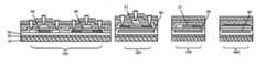
- FIG. 3 a to FIG. 3 dillustrate sectional diagrams of steps of a manufacturing method according to the present invention.
- an OLED displayis illustrated as an example.
- a switching TFT 100a driving TFT 200 , a photo sensor 300 and a capacitor (Cst) 400 of the OLED display
- a substrate 10having a first area and a second area is provided.
- the switching TFT 100is positioned on the first area.
- the driving TFT 200 , the photo sensor 300 and the capacitor 400are positioned on the second area.
- At least one buffer layer 20is formed on the substrate 10 .
- a buffer layer 20can be a nitride layer, such as a silicon nitride.
- Another buffer layer 30can be an oxide layer, such as silica.
- a heat sink layer 40can be formed on the buffer layer 30 of the driving TFT 200 , the photo sensor 300 and the capacitor 400 on the second area.
- a metal materialcan be chosen to form the heat sink layer 40 , such as molybdenum or molybdenum alloy.
- a further buffer layer 35is formed on the heat sink layer 40 .
- the material of the buffer layer 35can be silica as the same as the buffer layer 30 .
- the buffer layer 30 and the buffer layer 35cover the heat sink layer 40 on the second area as shown in FIG. 3 a.
- an amorphous silicon layer 50is formed to cover the buffer layer 30 and the buffer layer 35 .
- the amorphous silicon layer 50is then transformed into a poly silicon layer by ELA (Excimer Laser Anneal). Meanwhile, the poly silicon layer is patterned to form a first poly silicon layer 60 on the first area and a second poly silicon layer 61 on the second area as shown in FIG. 3 c .
- the heat sink layer 40is formed in advance on the second area where the driving TFT 200 , the photo sensor 300 and the capacitor 400 are formed, the heat sink phenomenon occurs on the second area during the crystallization process for transforming the amorphous silicon layer 50 into the first poly silicon layer 60 and the second poly silicon layer 61 by ELA.
- the heat sink layer 40is not formed on the first area where the switching TFT 100 are formed. Accordingly, the first poly silicon layer 60 on the first area and the second poly silicon layer 61 on the second area have different crystal grain sizes. Thereafter, with subsequent processes, the complete switching TFT 100 , the complete driving TFT 200 , the complete photo sensor 300 and the complete capacitor (Cst) 400 are manufactured as shown in FIG. 3 d.
- the first poly silicon layer 60is employed for manufacturing the switching TFT 100 and the second poly silicon layer 61 is employed for manufacturing the driving TFT 200 .
- the crystal grain size of the first poly silicon layer 60is larger than that of the second poly silicon layer 61 , and the mobility of the first poly silicon layer 60 is higher than that of the second poly silicon layer 61 .
- the high mobility demand for the switching TFT 100 and the small crystal grain size demand for the driving TFT 200can be satisfied. Therefore, the mura issue caused by the non-uniformity among the plural driving TFT 200 can be reduced.
- the heat sink layer 40which is positioned in correspondence to the photo sensor 300 , can be employed for reflecting light irradiating on the photo sensor 300 to increase the luminous sensitivity of the photo sensor 300 .
- the heat sink layer 40which is positioned in correspondence to the capacitor 400 can be employed as an electrode of the capacitor 400 and is connected with the capacitor 400 in parallel. Therefore, the occupied area of the capacitor 400 can be decreased to increase the aperture ratio of OLED display of the present invention.
- the poly silicon layers with different crystal grain sizes on the first area and the second areacan be formed in a single laser crystallization process according to the present invention.
- the present inventioncan solve the mura issue caused by forming the poly silicon layers with ELA. Therefore, the OLED display can acquire good luminance uniformity.
- the luminous sensitivity of the photo sensorcan be increased and the occupied area of the capacitor can be decreased, i.e. the aperture ratio of OLED display can be increased.
- the image display system of the present inventioncan be employed in a mobile phone, a digital camera, a personal digital assistance, a notebook, a laptop computer, a television, an in-vehicle display, a global positioning system, a flight display, a digital photo frame or a portable DVD player.
Landscapes
- Electroluminescent Light Sources (AREA)
- Recrystallisation Techniques (AREA)
- Thin Film Transistor (AREA)
- Devices For Indicating Variable Information By Combining Individual Elements (AREA)
Abstract
Description
Claims (11)
Applications Claiming Priority (3)
| Application Number | Priority Date | Filing Date | Title |
|---|---|---|---|
| TW97116022A | 2008-04-30 | ||
| TW097116022ATWI389211B (en) | 2008-04-30 | 2008-04-30 | Image display system and method of manufacturing same |
| TW097116022 | 2008-04-30 |
Publications (2)
| Publication Number | Publication Date |
|---|---|
| US20090272978A1 US20090272978A1 (en) | 2009-11-05 |
| US8115208B2true US8115208B2 (en) | 2012-02-14 |
Family
ID=41256522
Family Applications (1)
| Application Number | Title | Priority Date | Filing Date |
|---|---|---|---|
| US12/432,510Active2030-04-27US8115208B2 (en) | 2008-04-30 | 2009-04-29 | Image display system and manufacturing method thereof |
Country Status (3)
| Country | Link |
|---|---|
| US (1) | US8115208B2 (en) |
| JP (1) | JP5605823B2 (en) |
| TW (1) | TWI389211B (en) |
Cited By (1)
| Publication number | Priority date | Publication date | Assignee | Title |
|---|---|---|---|---|
| US20180026138A1 (en)* | 2016-07-19 | 2018-01-25 | Japan Display Inc. | TFT circuit board and display device having the same |
Families Citing this family (6)
| Publication number | Priority date | Publication date | Assignee | Title |
|---|---|---|---|---|
| KR101752400B1 (en)* | 2010-09-03 | 2017-06-30 | 삼성디스플레이 주식회사 | Method of forming polycrystalline silicon layer and thin film transistor and organic light emitting device including the polycrystalline silicon layer |
| WO2014024371A1 (en) | 2012-08-10 | 2014-02-13 | パナソニック株式会社 | Semiconductor light-emitting device |
| CN104465702B (en)* | 2014-11-03 | 2019-12-10 | 深圳市华星光电技术有限公司 | Manufacturing method of AMOLED (active matrix/organic light emitting diode) backboard |
| CN105514035B (en)* | 2016-01-21 | 2018-11-20 | 武汉华星光电技术有限公司 | The production method and low temperature polycrystalline silicon TFT substrate of low temperature polycrystalline silicon TFT substrate |
| US10388644B2 (en)* | 2016-11-29 | 2019-08-20 | Taiwan Semiconductor Manufacturing Company, Ltd. | Method of manufacturing conductors and semiconductor device which includes conductors |
| EP3970899B1 (en) | 2020-09-18 | 2023-11-22 | Laser Systems & Solutions of Europe | Method of and system for uniformly irradiating a frame of a processed substrate having a plurality of frames |
Citations (14)
| Publication number | Priority date | Publication date | Assignee | Title |
|---|---|---|---|---|
| US7166863B2 (en)* | 2002-03-15 | 2007-01-23 | Semiconductor Energy Laboratory Co. Ltd. | Semiconductor element, semiconductor device, electronic device, TV set and digital camera |
| US7259110B2 (en)* | 2004-04-28 | 2007-08-21 | Semiconductor Energy Laboratory Co., Ltd. | Manufacturing method of display device and semiconductor device |
| US7405033B2 (en)* | 2003-01-17 | 2008-07-29 | Semiconductor Energy Laboratory Co., Ltd. | Method for manufacturing resist pattern and method for manufacturing semiconductor device |
| US7491590B2 (en)* | 2004-05-28 | 2009-02-17 | Semiconductor Energy Laboratory Co., Ltd. | Method for manufacturing thin film transistor in display device |
| US7582904B2 (en)* | 2004-11-26 | 2009-09-01 | Semiconductor Energy Laboratory Co., Ltd. | Semiconductor device, display device and method for manufacturing thereof, and television device |
| US7615488B2 (en)* | 2004-03-19 | 2009-11-10 | Semiconductor Energy Laboratory Co., Ltd. | Method for forming pattern, thin film transistor, display device and method for manufacturing the same, and television device |
| US7635889B2 (en)* | 2005-01-28 | 2009-12-22 | Semiconductor Energy Laboratory Co., Ltd. | Semiconductor device, electronic device, and method of manufacturing semiconductor device |
| US7642038B2 (en)* | 2004-03-24 | 2010-01-05 | Semiconductor Energy Laboratory Co., Ltd. | Method for forming pattern, thin film transistor, display device, method for manufacturing thereof, and television apparatus |
| US7655566B2 (en)* | 2005-07-27 | 2010-02-02 | Semiconductor Energy Laboratory Co., Ltd. | Method for manufacturing semiconductor device |
| US7687326B2 (en)* | 2004-12-17 | 2010-03-30 | Semiconductor Energy Laboratory Co., Ltd. | Semiconductor device and manufacturing method thereof |
| US7727847B2 (en)* | 2006-08-24 | 2010-06-01 | Semiconductor Energy Laboratory Co., Ltd. | Method for manufacturing display device |
| US7732330B2 (en)* | 2005-06-30 | 2010-06-08 | Semiconductor Energy Laboratory Co., Ltd. | Semiconductor device and manufacturing method using an ink-jet method of the same |
| US7768617B2 (en)* | 2006-07-04 | 2010-08-03 | Semiconductor Energy Laboratory Co., Ltd. | Method for manufacturing a semiconductor device |
| US7807483B2 (en)* | 2006-07-28 | 2010-10-05 | Semiconductor Energy Laboratory Co., Ltd. | Method for manufacturing display device |
Family Cites Families (1)
| Publication number | Priority date | Publication date | Assignee | Title |
|---|---|---|---|---|
| US20080042131A1 (en)* | 2006-08-15 | 2008-02-21 | Tpo Displays Corp. | System for displaying images including thin film transistor device and method for fabricating the same |
- 2008
- 2008-04-30TWTW097116022Apatent/TWI389211B/ennot_activeIP Right Cessation
- 2009
- 2009-04-28JPJP2009109954Apatent/JP5605823B2/enactiveActive
- 2009-04-29USUS12/432,510patent/US8115208B2/enactiveActive
Patent Citations (14)
| Publication number | Priority date | Publication date | Assignee | Title |
|---|---|---|---|---|
| US7166863B2 (en)* | 2002-03-15 | 2007-01-23 | Semiconductor Energy Laboratory Co. Ltd. | Semiconductor element, semiconductor device, electronic device, TV set and digital camera |
| US7405033B2 (en)* | 2003-01-17 | 2008-07-29 | Semiconductor Energy Laboratory Co., Ltd. | Method for manufacturing resist pattern and method for manufacturing semiconductor device |
| US7615488B2 (en)* | 2004-03-19 | 2009-11-10 | Semiconductor Energy Laboratory Co., Ltd. | Method for forming pattern, thin film transistor, display device and method for manufacturing the same, and television device |
| US7642038B2 (en)* | 2004-03-24 | 2010-01-05 | Semiconductor Energy Laboratory Co., Ltd. | Method for forming pattern, thin film transistor, display device, method for manufacturing thereof, and television apparatus |
| US7259110B2 (en)* | 2004-04-28 | 2007-08-21 | Semiconductor Energy Laboratory Co., Ltd. | Manufacturing method of display device and semiconductor device |
| US7491590B2 (en)* | 2004-05-28 | 2009-02-17 | Semiconductor Energy Laboratory Co., Ltd. | Method for manufacturing thin film transistor in display device |
| US7582904B2 (en)* | 2004-11-26 | 2009-09-01 | Semiconductor Energy Laboratory Co., Ltd. | Semiconductor device, display device and method for manufacturing thereof, and television device |
| US7687326B2 (en)* | 2004-12-17 | 2010-03-30 | Semiconductor Energy Laboratory Co., Ltd. | Semiconductor device and manufacturing method thereof |
| US7635889B2 (en)* | 2005-01-28 | 2009-12-22 | Semiconductor Energy Laboratory Co., Ltd. | Semiconductor device, electronic device, and method of manufacturing semiconductor device |
| US7732330B2 (en)* | 2005-06-30 | 2010-06-08 | Semiconductor Energy Laboratory Co., Ltd. | Semiconductor device and manufacturing method using an ink-jet method of the same |
| US7655566B2 (en)* | 2005-07-27 | 2010-02-02 | Semiconductor Energy Laboratory Co., Ltd. | Method for manufacturing semiconductor device |
| US7768617B2 (en)* | 2006-07-04 | 2010-08-03 | Semiconductor Energy Laboratory Co., Ltd. | Method for manufacturing a semiconductor device |
| US7807483B2 (en)* | 2006-07-28 | 2010-10-05 | Semiconductor Energy Laboratory Co., Ltd. | Method for manufacturing display device |
| US7727847B2 (en)* | 2006-08-24 | 2010-06-01 | Semiconductor Energy Laboratory Co., Ltd. | Method for manufacturing display device |
Cited By (6)
| Publication number | Priority date | Publication date | Assignee | Title |
|---|---|---|---|---|
| US20180026138A1 (en)* | 2016-07-19 | 2018-01-25 | Japan Display Inc. | TFT circuit board and display device having the same |
| US11063154B2 (en)* | 2016-07-19 | 2021-07-13 | Japan Display Inc. | TFT circuit board and display device having the same |
| US20210305434A1 (en)* | 2016-07-19 | 2021-09-30 | Japan Display Inc. | Tft circuit board and display device having the same |
| US11742430B2 (en)* | 2016-07-19 | 2023-08-29 | Japan Display Inc. | TFT circuit board and display device having the same |
| US20230361220A1 (en)* | 2016-07-19 | 2023-11-09 | Japan Display Inc. | Tft circuit board and display device having the same |
| US12166135B2 (en)* | 2016-07-19 | 2024-12-10 | Japan Display Inc. | TFT circuit board and display device having the same |
Also Published As
| Publication number | Publication date |
|---|---|
| US20090272978A1 (en) | 2009-11-05 |
| JP5605823B2 (en) | 2014-10-15 |
| TW200945446A (en) | 2009-11-01 |
| TWI389211B (en) | 2013-03-11 |
| JP2009272625A (en) | 2009-11-19 |
Similar Documents
| Publication | Publication Date | Title |
|---|---|---|
| US8115208B2 (en) | Image display system and manufacturing method thereof | |
| US8183064B2 (en) | Thin film transistor devices for OLED displays and method for fabricating the same | |
| US10103173B2 (en) | Manufacture method of array substrate and array substrate manufactured by the method | |
| US7592628B2 (en) | Display with thin film transistor devices having different electrical characteristics in pixel and driving regions | |
| US20090203160A1 (en) | System for displaying images including thin film transistor device and method for fabricating the same | |
| US20080087889A1 (en) | Method of fabricating an organic electroluminescent device and system of displaying images | |
| US20160300900A1 (en) | Display Device | |
| US7498210B2 (en) | LTPS-LCD structure and method for manufacturing the same | |
| US11171159B2 (en) | Display backplane and method for manufacturing the same, display panel and display device | |
| US8158985B2 (en) | Thin film transistor devices with different electrical characteristics and method for fabricating the same | |
| CN108807420B (en) | Flexible display substrate, manufacturing method thereof and foldable display device | |
| JP7656586B2 (en) | Semiconductor Device | |
| US20100252833A1 (en) | Thin film transistor devices having transistors with different electrical characteristics and method for fabricating the same | |
| US7557498B2 (en) | System for displaying images including electroluminescent device and method for fabricating the same | |
| US11626429B2 (en) | Display device and method of fabricating the same | |
| US20210335981A1 (en) | Display panel, manufacturing method thereof and related display device | |
| US11532679B2 (en) | Method of fabricating array substrate, array substrate, and display apparatus | |
| US8299471B2 (en) | Organic electroluminescent device and fabrication method thereof | |
| CN101789434B (en) | Image display system and manufacturing method thereof | |
| CN101546732B (en) | Method for manufacturing thin film transistor and display with same | |
| CN101593730A (en) | Image display system and method for manufacturing the same | |
| EP4210035A1 (en) | Display panel, manufacturing method for display panel, and electronic device | |
| JP2025159017A (en) | Semiconductor Devices | |
| TW200407051A (en) | Active matrix organic light emitting diode and method of manufacturing the same |
Legal Events
| Date | Code | Title | Description |
|---|---|---|---|
| AS | Assignment | Owner name:TPO DISPLAYS CORP., TAIWAN Free format text:ASSIGNMENT OF ASSIGNORS INTEREST;ASSIGNORS:LIU, YU-CHUNG;LEE, TE-YU;REEL/FRAME:022616/0154 Effective date:20090423 | |
| AS | Assignment | Owner name:CHIMEI INNOLUX CORPORATION, TAIWAN Free format text:MERGER;ASSIGNOR:TPO DISPLAYS CORP.;REEL/FRAME:025738/0274 Effective date:20100318 | |
| STCF | Information on status: patent grant | Free format text:PATENTED CASE | |
| AS | Assignment | Owner name:INNOLUX CORPORATION, TAIWAN Free format text:CHANGE OF NAME;ASSIGNOR:CHIMEI INNOLUX CORPORATION;REEL/FRAME:032621/0718 Effective date:20121219 | |
| FPAY | Fee payment | Year of fee payment:4 | |
| MAFP | Maintenance fee payment | Free format text:PAYMENT OF MAINTENANCE FEE, 8TH YEAR, LARGE ENTITY (ORIGINAL EVENT CODE: M1552); ENTITY STATUS OF PATENT OWNER: LARGE ENTITY Year of fee payment:8 | |
| MAFP | Maintenance fee payment | Free format text:PAYMENT OF MAINTENANCE FEE, 12TH YEAR, LARGE ENTITY (ORIGINAL EVENT CODE: M1553); ENTITY STATUS OF PATENT OWNER: LARGE ENTITY Year of fee payment:12 | |
| AS | Assignment | Owner name:RED OAK INNOVATIONS LIMITED, IRELAND Free format text:ASSIGNMENT OF ASSIGNORS INTEREST;ASSIGNOR:INNOLUX CORPORATION;REEL/FRAME:069206/0903 Effective date:20240925 |