US8115112B2 - Interposer substrates and semiconductor device assemblies and electronic systems including such interposer substrates - Google Patents
Interposer substrates and semiconductor device assemblies and electronic systems including such interposer substratesDownload PDFInfo
- Publication number
- US8115112B2 US8115112B2US12/201,222US20122208AUS8115112B2US 8115112 B2US8115112 B2US 8115112B2US 20122208 AUS20122208 AUS 20122208AUS 8115112 B2US8115112 B2US 8115112B2
- Authority
- US
- United States
- Prior art keywords
- recess
- core member
- semiconductor die
- interposer substrate
- electrically conductive
- Prior art date
- Legal status (The legal status is an assumption and is not a legal conclusion. Google has not performed a legal analysis and makes no representation as to the accuracy of the status listed.)
- Active, expires
Links
Images


Classifications
- H—ELECTRICITY
- H01—ELECTRIC ELEMENTS
- H01L—SEMICONDUCTOR DEVICES NOT COVERED BY CLASS H10
- H01L23/00—Details of semiconductor or other solid state devices
- H01L23/02—Containers; Seals
- H—ELECTRICITY
- H01—ELECTRIC ELEMENTS
- H01L—SEMICONDUCTOR DEVICES NOT COVERED BY CLASS H10
- H01L23/00—Details of semiconductor or other solid state devices
- H01L23/12—Mountings, e.g. non-detachable insulating substrates
- H01L23/13—Mountings, e.g. non-detachable insulating substrates characterised by the shape
- H—ELECTRICITY
- H01—ELECTRIC ELEMENTS
- H01L—SEMICONDUCTOR DEVICES NOT COVERED BY CLASS H10
- H01L23/00—Details of semiconductor or other solid state devices
- H01L23/28—Encapsulations, e.g. encapsulating layers, coatings, e.g. for protection
- H01L23/31—Encapsulations, e.g. encapsulating layers, coatings, e.g. for protection characterised by the arrangement or shape
- H01L23/3107—Encapsulations, e.g. encapsulating layers, coatings, e.g. for protection characterised by the arrangement or shape the device being completely enclosed
- H01L23/3121—Encapsulations, e.g. encapsulating layers, coatings, e.g. for protection characterised by the arrangement or shape the device being completely enclosed a substrate forming part of the encapsulation
- H01L23/3128—Encapsulations, e.g. encapsulating layers, coatings, e.g. for protection characterised by the arrangement or shape the device being completely enclosed a substrate forming part of the encapsulation the substrate having spherical bumps for external connection
- H—ELECTRICITY
- H01—ELECTRIC ELEMENTS
- H01L—SEMICONDUCTOR DEVICES NOT COVERED BY CLASS H10
- H01L23/00—Details of semiconductor or other solid state devices
- H01L23/34—Arrangements for cooling, heating, ventilating or temperature compensation ; Temperature sensing arrangements
- H01L23/36—Selection of materials, or shaping, to facilitate cooling or heating, e.g. heatsinks
- H01L23/373—Cooling facilitated by selection of materials for the device or materials for thermal expansion adaptation, e.g. carbon
- H01L23/3735—Laminates or multilayers, e.g. direct bond copper ceramic substrates
- H—ELECTRICITY
- H01—ELECTRIC ELEMENTS
- H01L—SEMICONDUCTOR DEVICES NOT COVERED BY CLASS H10
- H01L23/00—Details of semiconductor or other solid state devices
- H01L23/52—Arrangements for conducting electric current within the device in operation from one component to another, i.e. interconnections, e.g. wires, lead frames
- H01L23/538—Arrangements for conducting electric current within the device in operation from one component to another, i.e. interconnections, e.g. wires, lead frames the interconnection structure between a plurality of semiconductor chips being formed on, or in, insulating substrates
- H01L23/5387—Flexible insulating substrates
- H—ELECTRICITY
- H01—ELECTRIC ELEMENTS
- H01L—SEMICONDUCTOR DEVICES NOT COVERED BY CLASS H10
- H01L25/00—Assemblies consisting of a plurality of semiconductor or other solid state devices
- H01L25/03—Assemblies consisting of a plurality of semiconductor or other solid state devices all the devices being of a type provided for in a single subclass of subclasses H10B, H10D, H10F, H10H, H10K or H10N, e.g. assemblies of rectifier diodes
- H01L25/10—Assemblies consisting of a plurality of semiconductor or other solid state devices all the devices being of a type provided for in a single subclass of subclasses H10B, H10D, H10F, H10H, H10K or H10N, e.g. assemblies of rectifier diodes the devices having separate containers
- H01L25/105—Assemblies consisting of a plurality of semiconductor or other solid state devices all the devices being of a type provided for in a single subclass of subclasses H10B, H10D, H10F, H10H, H10K or H10N, e.g. assemblies of rectifier diodes the devices having separate containers the devices being integrated devices of class H10
- B—PERFORMING OPERATIONS; TRANSPORTING
- B33—ADDITIVE MANUFACTURING TECHNOLOGY
- B33Y—ADDITIVE MANUFACTURING, i.e. MANUFACTURING OF THREE-DIMENSIONAL [3-D] OBJECTS BY ADDITIVE DEPOSITION, ADDITIVE AGGLOMERATION OR ADDITIVE LAYERING, e.g. BY 3-D PRINTING, STEREOLITHOGRAPHY OR SELECTIVE LASER SINTERING
- B33Y80/00—Products made by additive manufacturing
- H—ELECTRICITY
- H01—ELECTRIC ELEMENTS
- H01L—SEMICONDUCTOR DEVICES NOT COVERED BY CLASS H10
- H01L2224/00—Indexing scheme for arrangements for connecting or disconnecting semiconductor or solid-state bodies and methods related thereto as covered by H01L24/00
- H01L2224/01—Means for bonding being attached to, or being formed on, the surface to be connected, e.g. chip-to-package, die-attach, "first-level" interconnects; Manufacturing methods related thereto
- H01L2224/26—Layer connectors, e.g. plate connectors, solder or adhesive layers; Manufacturing methods related thereto
- H01L2224/31—Structure, shape, material or disposition of the layer connectors after the connecting process
- H01L2224/32—Structure, shape, material or disposition of the layer connectors after the connecting process of an individual layer connector
- H01L2224/321—Disposition
- H01L2224/32151—Disposition the layer connector connecting between a semiconductor or solid-state body and an item not being a semiconductor or solid-state body, e.g. chip-to-substrate, chip-to-passive
- H01L2224/32221—Disposition the layer connector connecting between a semiconductor or solid-state body and an item not being a semiconductor or solid-state body, e.g. chip-to-substrate, chip-to-passive the body and the item being stacked
- H01L2224/32225—Disposition the layer connector connecting between a semiconductor or solid-state body and an item not being a semiconductor or solid-state body, e.g. chip-to-substrate, chip-to-passive the body and the item being stacked the item being non-metallic, e.g. insulating substrate with or without metallisation
- H—ELECTRICITY
- H01—ELECTRIC ELEMENTS
- H01L—SEMICONDUCTOR DEVICES NOT COVERED BY CLASS H10
- H01L2224/00—Indexing scheme for arrangements for connecting or disconnecting semiconductor or solid-state bodies and methods related thereto as covered by H01L24/00
- H01L2224/01—Means for bonding being attached to, or being formed on, the surface to be connected, e.g. chip-to-package, die-attach, "first-level" interconnects; Manufacturing methods related thereto
- H01L2224/42—Wire connectors; Manufacturing methods related thereto
- H01L2224/47—Structure, shape, material or disposition of the wire connectors after the connecting process
- H01L2224/48—Structure, shape, material or disposition of the wire connectors after the connecting process of an individual wire connector
- H01L2224/4805—Shape
- H01L2224/4809—Loop shape
- H01L2224/48091—Arched
- H—ELECTRICITY
- H01—ELECTRIC ELEMENTS
- H01L—SEMICONDUCTOR DEVICES NOT COVERED BY CLASS H10
- H01L2224/00—Indexing scheme for arrangements for connecting or disconnecting semiconductor or solid-state bodies and methods related thereto as covered by H01L24/00
- H01L2224/01—Means for bonding being attached to, or being formed on, the surface to be connected, e.g. chip-to-package, die-attach, "first-level" interconnects; Manufacturing methods related thereto
- H01L2224/42—Wire connectors; Manufacturing methods related thereto
- H01L2224/47—Structure, shape, material or disposition of the wire connectors after the connecting process
- H01L2224/48—Structure, shape, material or disposition of the wire connectors after the connecting process of an individual wire connector
- H01L2224/481—Disposition
- H01L2224/48151—Connecting between a semiconductor or solid-state body and an item not being a semiconductor or solid-state body, e.g. chip-to-substrate, chip-to-passive
- H01L2224/48221—Connecting between a semiconductor or solid-state body and an item not being a semiconductor or solid-state body, e.g. chip-to-substrate, chip-to-passive the body and the item being stacked
- H01L2224/48225—Connecting between a semiconductor or solid-state body and an item not being a semiconductor or solid-state body, e.g. chip-to-substrate, chip-to-passive the body and the item being stacked the item being non-metallic, e.g. insulating substrate with or without metallisation
- H01L2224/48227—Connecting between a semiconductor or solid-state body and an item not being a semiconductor or solid-state body, e.g. chip-to-substrate, chip-to-passive the body and the item being stacked the item being non-metallic, e.g. insulating substrate with or without metallisation connecting the wire to a bond pad of the item
- H—ELECTRICITY
- H01—ELECTRIC ELEMENTS
- H01L—SEMICONDUCTOR DEVICES NOT COVERED BY CLASS H10
- H01L2224/00—Indexing scheme for arrangements for connecting or disconnecting semiconductor or solid-state bodies and methods related thereto as covered by H01L24/00
- H01L2224/01—Means for bonding being attached to, or being formed on, the surface to be connected, e.g. chip-to-package, die-attach, "first-level" interconnects; Manufacturing methods related thereto
- H01L2224/42—Wire connectors; Manufacturing methods related thereto
- H01L2224/47—Structure, shape, material or disposition of the wire connectors after the connecting process
- H01L2224/48—Structure, shape, material or disposition of the wire connectors after the connecting process of an individual wire connector
- H01L2224/481—Disposition
- H01L2224/48151—Connecting between a semiconductor or solid-state body and an item not being a semiconductor or solid-state body, e.g. chip-to-substrate, chip-to-passive
- H01L2224/48221—Connecting between a semiconductor or solid-state body and an item not being a semiconductor or solid-state body, e.g. chip-to-substrate, chip-to-passive the body and the item being stacked
- H01L2224/48225—Connecting between a semiconductor or solid-state body and an item not being a semiconductor or solid-state body, e.g. chip-to-substrate, chip-to-passive the body and the item being stacked the item being non-metallic, e.g. insulating substrate with or without metallisation
- H01L2224/4824—Connecting between the body and an opposite side of the item with respect to the body
- H—ELECTRICITY
- H01—ELECTRIC ELEMENTS
- H01L—SEMICONDUCTOR DEVICES NOT COVERED BY CLASS H10
- H01L2224/00—Indexing scheme for arrangements for connecting or disconnecting semiconductor or solid-state bodies and methods related thereto as covered by H01L24/00
- H01L2224/73—Means for bonding being of different types provided for in two or more of groups H01L2224/10, H01L2224/18, H01L2224/26, H01L2224/34, H01L2224/42, H01L2224/50, H01L2224/63, H01L2224/71
- H01L2224/732—Location after the connecting process
- H01L2224/73201—Location after the connecting process on the same surface
- H01L2224/73215—Layer and wire connectors
- H—ELECTRICITY
- H01—ELECTRIC ELEMENTS
- H01L—SEMICONDUCTOR DEVICES NOT COVERED BY CLASS H10
- H01L2225/00—Details relating to assemblies covered by the group H01L25/00 but not provided for in its subgroups
- H01L2225/03—All the devices being of a type provided for in the same main group of the same subclass of class H10, e.g. assemblies of rectifier diodes
- H01L2225/10—All the devices being of a type provided for in the same main group of the same subclass of class H10, e.g. assemblies of rectifier diodes the devices having separate containers
- H01L2225/1005—All the devices being of a type provided for in the same main group of the same subclass of class H10, e.g. assemblies of rectifier diodes the devices having separate containers the devices being integrated devices of class H10
- H01L2225/1011—All the devices being of a type provided for in the same main group of the same subclass of class H10, e.g. assemblies of rectifier diodes the devices having separate containers the devices being integrated devices of class H10 the containers being in a stacked arrangement
- H01L2225/1041—Special adaptations for top connections of the lowermost container, e.g. redistribution layer, integral interposer
- H—ELECTRICITY
- H01—ELECTRIC ELEMENTS
- H01L—SEMICONDUCTOR DEVICES NOT COVERED BY CLASS H10
- H01L2225/00—Details relating to assemblies covered by the group H01L25/00 but not provided for in its subgroups
- H01L2225/03—All the devices being of a type provided for in the same main group of the same subclass of class H10, e.g. assemblies of rectifier diodes
- H01L2225/10—All the devices being of a type provided for in the same main group of the same subclass of class H10, e.g. assemblies of rectifier diodes the devices having separate containers
- H01L2225/1005—All the devices being of a type provided for in the same main group of the same subclass of class H10, e.g. assemblies of rectifier diodes the devices having separate containers the devices being integrated devices of class H10
- H01L2225/1011—All the devices being of a type provided for in the same main group of the same subclass of class H10, e.g. assemblies of rectifier diodes the devices having separate containers the devices being integrated devices of class H10 the containers being in a stacked arrangement
- H01L2225/1047—Details of electrical connections between containers
- H01L2225/1058—Bump or bump-like electrical connections, e.g. balls, pillars, posts
- H—ELECTRICITY
- H01—ELECTRIC ELEMENTS
- H01L—SEMICONDUCTOR DEVICES NOT COVERED BY CLASS H10
- H01L24/00—Arrangements for connecting or disconnecting semiconductor or solid-state bodies; Methods or apparatus related thereto
- H01L24/01—Means for bonding being attached to, or being formed on, the surface to be connected, e.g. chip-to-package, die-attach, "first-level" interconnects; Manufacturing methods related thereto
- H01L24/42—Wire connectors; Manufacturing methods related thereto
- H01L24/47—Structure, shape, material or disposition of the wire connectors after the connecting process
- H01L24/48—Structure, shape, material or disposition of the wire connectors after the connecting process of an individual wire connector
- H—ELECTRICITY
- H01—ELECTRIC ELEMENTS
- H01L—SEMICONDUCTOR DEVICES NOT COVERED BY CLASS H10
- H01L2924/00—Indexing scheme for arrangements or methods for connecting or disconnecting semiconductor or solid-state bodies as covered by H01L24/00
- H01L2924/0001—Technical content checked by a classifier
- H01L2924/00014—Technical content checked by a classifier the subject-matter covered by the group, the symbol of which is combined with the symbol of this group, being disclosed without further technical details
- H—ELECTRICITY
- H01—ELECTRIC ELEMENTS
- H01L—SEMICONDUCTOR DEVICES NOT COVERED BY CLASS H10
- H01L2924/00—Indexing scheme for arrangements or methods for connecting or disconnecting semiconductor or solid-state bodies as covered by H01L24/00
- H01L2924/01—Chemical elements
- H01L2924/01019—Potassium [K]
- H—ELECTRICITY
- H01—ELECTRIC ELEMENTS
- H01L—SEMICONDUCTOR DEVICES NOT COVERED BY CLASS H10
- H01L2924/00—Indexing scheme for arrangements or methods for connecting or disconnecting semiconductor or solid-state bodies as covered by H01L24/00
- H01L2924/01—Chemical elements
- H01L2924/01078—Platinum [Pt]
- H—ELECTRICITY
- H01—ELECTRIC ELEMENTS
- H01L—SEMICONDUCTOR DEVICES NOT COVERED BY CLASS H10
- H01L2924/00—Indexing scheme for arrangements or methods for connecting or disconnecting semiconductor or solid-state bodies as covered by H01L24/00
- H01L2924/01—Chemical elements
- H01L2924/01087—Francium [Fr]
- H—ELECTRICITY
- H01—ELECTRIC ELEMENTS
- H01L—SEMICONDUCTOR DEVICES NOT COVERED BY CLASS H10
- H01L2924/00—Indexing scheme for arrangements or methods for connecting or disconnecting semiconductor or solid-state bodies as covered by H01L24/00
- H01L2924/095—Indexing scheme for arrangements or methods for connecting or disconnecting semiconductor or solid-state bodies as covered by H01L24/00 with a principal constituent of the material being a combination of two or more materials provided in the groups H01L2924/013 - H01L2924/0715
- H01L2924/097—Glass-ceramics, e.g. devitrified glass
- H01L2924/09701—Low temperature co-fired ceramic [LTCC]
- H—ELECTRICITY
- H01—ELECTRIC ELEMENTS
- H01L—SEMICONDUCTOR DEVICES NOT COVERED BY CLASS H10
- H01L2924/00—Indexing scheme for arrangements or methods for connecting or disconnecting semiconductor or solid-state bodies as covered by H01L24/00
- H01L2924/10—Details of semiconductor or other solid state devices to be connected
- H01L2924/11—Device type
- H01L2924/14—Integrated circuits
- H—ELECTRICITY
- H01—ELECTRIC ELEMENTS
- H01L—SEMICONDUCTOR DEVICES NOT COVERED BY CLASS H10
- H01L2924/00—Indexing scheme for arrangements or methods for connecting or disconnecting semiconductor or solid-state bodies as covered by H01L24/00
- H01L2924/15—Details of package parts other than the semiconductor or other solid state devices to be connected
- H01L2924/151—Die mounting substrate
- H01L2924/1515—Shape
- H01L2924/15153—Shape the die mounting substrate comprising a recess for hosting the device
- H—ELECTRICITY
- H01—ELECTRIC ELEMENTS
- H01L—SEMICONDUCTOR DEVICES NOT COVERED BY CLASS H10
- H01L2924/00—Indexing scheme for arrangements or methods for connecting or disconnecting semiconductor or solid-state bodies as covered by H01L24/00
- H01L2924/15—Details of package parts other than the semiconductor or other solid state devices to be connected
- H01L2924/151—Die mounting substrate
- H01L2924/153—Connection portion
- H01L2924/1531—Connection portion the connection portion being formed only on the surface of the substrate opposite to the die mounting surface
- H01L2924/15311—Connection portion the connection portion being formed only on the surface of the substrate opposite to the die mounting surface being a ball array, e.g. BGA
- H—ELECTRICITY
- H01—ELECTRIC ELEMENTS
- H01L—SEMICONDUCTOR DEVICES NOT COVERED BY CLASS H10
- H01L2924/00—Indexing scheme for arrangements or methods for connecting or disconnecting semiconductor or solid-state bodies as covered by H01L24/00
- H01L2924/15—Details of package parts other than the semiconductor or other solid state devices to be connected
- H01L2924/181—Encapsulation
- H—ELECTRICITY
- H01—ELECTRIC ELEMENTS
- H01L—SEMICONDUCTOR DEVICES NOT COVERED BY CLASS H10
- H01L2924/00—Indexing scheme for arrangements or methods for connecting or disconnecting semiconductor or solid-state bodies as covered by H01L24/00
- H01L2924/30—Technical effects
- H01L2924/301—Electrical effects
- H01L2924/3025—Electromagnetic shielding
- Y—GENERAL TAGGING OF NEW TECHNOLOGICAL DEVELOPMENTS; GENERAL TAGGING OF CROSS-SECTIONAL TECHNOLOGIES SPANNING OVER SEVERAL SECTIONS OF THE IPC; TECHNICAL SUBJECTS COVERED BY FORMER USPC CROSS-REFERENCE ART COLLECTIONS [XRACs] AND DIGESTS
- Y10—TECHNICAL SUBJECTS COVERED BY FORMER USPC
- Y10T—TECHNICAL SUBJECTS COVERED BY FORMER US CLASSIFICATION
- Y10T29/00—Metal working
- Y10T29/49—Method of mechanical manufacture
- Y10T29/49002—Electrical device making
- Y10T29/49117—Conductor or circuit manufacturing
- Y10T29/49124—On flat or curved insulated base, e.g., printed circuit, etc.
Definitions
- Embodiments of the inventionrelate to chip-scale packages (CSPs), stacking integrated such CSPs in a multi-chip module (MCM) structure in a package-on-package (POP) configuration, and methods of forming such packages and structures.
- CSPschip-scale packages
- MCMmulti-chip module
- POPpackage-on-package
- Semiconductor diceare conventionally packaged individually in transfer-molded resin packages or, less commonly, ceramic packages.
- Packaging supportsprotects, and (in some instances) dissipates heat from the semiconductor die and provides a lead system for power and ground or bias, as well as signal distribution to and from the semiconductor die or dice within.
- the die packagemay also facilitate burn-in and other testing of each semiconductor die or dice in the package prior to and after its assembly with higher-level packaging.
- Chip-scale packageOne type of integrated circuit (IC) or semiconductor die package is referred to as a “chip-scale package,” “chip-size package,” or merely “CSP.” These designations relate to the physical dimensions of the package, which are only nominally larger than the actual dimensions (length, width, and height) of the unpackaged semiconductor die.
- Chip-scale packagesmay be fabricated in “uncased” or “cased” configurations. Uncased chip-scale packages do not include encapsulation or other covering of the sides of a semiconductor die extending between the active surface and back side thereof, and thus exhibit a “footprint” (peripheral outline) that is substantially the same as that of an unpackaged semiconductor die.
- Cased chip-scale packageshave encapsulated or otherwise covered sides and thus exhibit a peripheral outline that is slightly larger than that of an unpackaged semiconductor die.
- a surface area of a footprint for a conventional cased chip-scale packagemay be up to about 1.2 times that of the bare semiconductor die contained within the package.
- a chip-scale packagemay include an interposer substrate bonded to a surface of the semiconductor die.
- the interposer substrateconventionally includes traces extending to contacts for making external electrical connections to the semiconductor die of the chip-scale package.
- the interposer substrate for a chip-scale packagemay conventionally comprise a flexible material, such as a polymer (i.e., polyimide) tape such as KAPTON® tape, or a rigid material, such as silicon, ceramic, glass, BT (Bismaleimide Triazine) resin, or an FR-4 or other fiberglass laminate.
- the external contacts for one type of chip-scale packageinclude solder balls or other discrete conductive elements protruding from the package and arranged in an array.
- BGAball grid array
- FBGAfine ball grid array
- Integrated circuit packaging surface mount technologysuch as so-called “vertical surface mount packages” or “VSMP” technology
- VSMPvertical surface mount packages
- This configurationresults in more compact designs and form factors and a significant increase in integrated circuit density.
- many VSMP designsare somewhat costly to implement and require fairly complex and sophisticated carrier substrates.
- the relatively large distance of protrusion of the VSMPs above the carrier substrateis unacceptable for compact applications where vertical height is an issue and, for other applications unacceptably limits the number of carrier substrates which may be inserted transversely in adjacent slots of a higher-level packaging substrate, such as a PC motherboard.
- Chip-scale packagesare thus of current interest in modern semiconductor packaging as a method for reducing both package size and cost. Further, the industry has responded to the limited space or “real estate” available for mounting semiconductor dice on a carrier substrate by vertically stacking two or more semiconductor dice, the I/Os of the die stack connecting to the carrier substrate often being provided between the lowermost semiconductor die and carrier substrate within the footprint of the stack. Therefore, it would be advantageous to provide a method and apparatus that may further reduce chip-scale package size and enhance robustness and heat transfer capabilities of the package while at the same time reduce fabrication cost and enhance production flexibility in combination with providing a capability to stack two or more semiconductor dice of the same or different types to increase circuit density on a carrier substrate to which such a multi-die chip-scale package is attached.
- FIG. 1is an embodiment of a Board-On-Chip package-on-package assembly according to an embodiment of the present invention
- FIG. 2is an embodiment of a Chip-On-Board package-on-package assembly according to an embodiment of the present invention
- FIG. 3depicts an embodiment of a sequence of acts in a method of manufacturing a Board-On-Chip assembly according to an embodiment of the present invention
- FIG. 4depicts an embodiment of a sequence of acts in a method of manufacturing a Chip-On-Board assembly according to an embodiment of the present invention.
- FIG. 5depicts a block diagram of a system including semiconductor dice packaged in accordance with one or more embodiments of the present invention.
- Embodiments of chip-scale packagesare disclosed, as well as to embodiments of methods of fabricating such packages including, by way of example only, Chip-On-Board (COB) and Board-On-Chip (BOC) packages. Also disclosed are embodiments of vertically stacked Package-On-Package (POP) modules, and systems including COB and BOC packages and POP modules.
- COBChip-On-Board
- BOCBoard-On-Chip
- POPvertically stacked Package-On-Package
- Embodiments of the chip-scale packagemay include a core member formed from a metal or metal alloy and having at least one portion partially folded over itself. These embodiments provide a minimized footprint, substantially chip-scale package of robust design exhibiting enhanced rigidity that provides a capability of stacking multiple semiconductor dice. Such embodiments also provide a capability to convert semiconductor dice exhibiting a peripheral or central bond pad I/O arrangement into array-type chip-scale packages. Yet a further advantage of the various embodiments of chip-scale packages of the present invention is improved thermal and circuit performance.
- the present inventionin various embodiments, relates to chip-scale packages exhibiting arrays of external contacts, as well as to methods of fabricating such packages including, by way of example only, ball grid array chip-scale packages.
- One embodiment of the inventioncomprises an interposer substrate that includes a core member.
- the core memberprovides, among others, a die attach area for receiving a semiconductor die and at least one folded flange member that extends both laterally away from and back toward and above the die attach area. Two opposing flange members may be employed.
- the interposer substrateprovides signal, ground or bias and power routing structures that are insulated from the core member by a dielectric material that may be at least partially supported by the flange members.
- the routing structuresmay further include conductive elements that provide electrical communication to the semiconductor die, another package, a carrier substrate, and the like.
- a semiconductor die with a plurality of bond pads on an active surfacemay be disposed over a die attach area of a core member of the interposer substrate with the active surface of the die disposed, face down, on the die attach area.
- the plurality of bond padsmay be accessible through at least one aperture in the form of a groove or slot formed in the core member that corresponds to the location of the plurality of bond pads.
- Flange members of the interposer substratemay extend laterally away from the semiconductor die attach area on opposing sides thereof and fold back over at least a portion of the core member toward the semiconductor die.
- the interposer substrateprovides signal, ground or bias and power routing structures that are insulated from the core member by a dielectric material that may be at least partially supported by the flange members.
- the routing structuresmay include conductive traces that provide electrical communication paths to locations proximate the bond pads of the semiconductor die.
- the conductive tracesmay also provide electrical communication to other conductive interconnects for external connection and which may include discrete conductive elements in the form of pads or lands, balls, bumps, studs, columns, pillars, or pins.
- At least a second semiconductor device assemblymay be stacked with the first semiconductor device assembly in a substantially superimposed manner.
- the conductive interconnectsmay be used to provide electrical communication, as well as thermal conduction, between the stacked semiconductor device assemblies.
- Yet another embodiment of the inventionincludes a chip-on-board (COB) semiconductor device assembly.
- a semiconductor die with a plurality of bond pads on an active surfacemay be disposed over and secured by its back side to a die attach area of an insulative layer located within a cavity of a core member of the interposer substrate.
- Flange members of the core membermay extend laterally from the semiconductor die attach area on opposing sides thereof and fold back over at least a portion of the core member toward the semiconductor die.
- the interposer substrateprovides signal, ground or bias and power routing structures that are insulated from the core member by a dielectric material and at least partially supported by the flange members.
- the routing structuresmay include conductive traces that provide electrical communication to locations proximate the bond pads of the semiconductor die.
- the conductive tracesprovide electrical communication to other conductive interconnects, which may comprise discrete conductive elements in the form of pads or lands, balls, bumps, studs, columns or pillars, pins or other conductive elements, or other conductive structures such as a Z-axis (anisotropic) conductive film.
- conductive interconnectsmay comprise discrete conductive elements in the form of pads or lands, balls, bumps, studs, columns or pillars, pins or other conductive elements, or other conductive structures such as a Z-axis (anisotropic) conductive film.
- At least a second semiconductor device assemblymay be stacked with the first semiconductor device assembly in a substantially superimposed manner.
- the conductive interconnectsmay provide electrical communication, as well as thermal conduction, between the stacked semiconductor device assemblies.
- Embodiments of methods of fabricating the chip-scale packages of the present invention, as well as assemblies of higher-level packaging incorporating the inventive packagesare also encompassed by the invention.
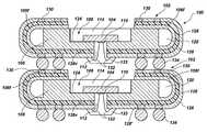
- FIG. 1A first embodiment of a Board-On-Chip (BOC) package-on-package assembly 100 according to the present invention may be seen in FIG. 1 .
- the BOC semiconductor device assemblies 102 included in package-on-package (POP) assembly 100 depicted in FIG. 1each include an electronic device, such as a semiconductor die 104 , may be disposed with its active surface facing downward upon a core member 106 , in an upward-facing (as the drawing is oriented), substantially central recess 108 thereof with bond pads 110 of semiconductor die 104 exposed through at least one aperture 112 configured as a groove or slot extending through core member 106 from central recess 108 to an opposing surface thereof.
- POPpackage-on-package
- Core member 106may comprise, by way of example only, copper or Alloy 42, a nickel-iron alloy. Aluminum and aluminum alloys may also be suitable materials.
- Each BOC semiconductor device assembly 102may further include a dielectric layer 126 , such as a polyimide layer, surrounding aperture 112 and extending over the opposing surface of core member 106 .
- Conductive traces 128are disposed over dielectric layer 126 and extend from locations adjacent aperture 112 around the exterior surface of dielectric layer 126 to terminate at terminal pads 130 on the opposing side of the BOC semiconductor device assembly 102 .
- conductive tracesis used herein in a nonlimiting sense, and may comprise, for example, metal conductive paths in the form of thin sheet material, stenciled conductive paths, or conductive paths of other materials and configurations.
- Terminal pads 130may comprise enlarged segments of conductive traces 128 .
- Conductive elements 132 in the form of, for example, wire bonds or traces on dielectric tape comprising TAB (tape automated bonding) type connectionsmay be used to connect the semiconductor die 104 to the conductive traces 128 .
- a dielectric material 133may be employed to fill the at least one aperture 112 and cover bond pads 110 , conductive elements 132 and the connection thereof to proximate ends of conductive traces 128 .
- Conductive interconnects in the form of discrete conductive elements 134may be formed on at least some of the conductive traces 128 on the underside (as the drawing figure is oriented) of each BOC semiconductor device assembly 102 , on enlarged portions 128 ′ thereof as shown.
- Discrete conductive elements 134may comprise, for example, pads or lands, balls, bumps, studs, columns or pillars, pins or other discrete conductive elements.
- Discrete conductive elements 134may comprise a metal, an alloy (including, for example, solders), a metal or alloy-covered nonconductive element, a conductive epoxy, or a conductor-filled epoxy, by way of example only.
- the core member 106may provide a rigid platform from which a semiconductor package may be formed; the core member 106 may provide sufficient rigidity to the package so that the core member 106 can be run on existing semiconductor assembly lines developed for processing of lead frame-based packages. As noted above, the core member 106 may have a recess 108 for receiving an electronic device such as a semiconductor die 104 and at least one aperture 112 that extends through the core member 106 from recess 108 to the exterior of the dielectric layer 126 adjacent ends of conductive traces 128 .
- the at least one aperture 112may be a single hole, a series of holes, a slot, or other shape having dimensions that expose bond pads 110 on the active surface of semiconductor die 104 therethrough and enable conductive elements 132 to be extended between bond pads 110 and adjacent ends of conductive traces 128 disposed on dielectric layer 126 .
- bond pads 110extend in parallel rows along and transverse to a centerline of semiconductor die 104 (which, in the example shown, lies perpendicular to the drawing sheet), and the at least one aperture 112 comprises a slot.
- active surface of semiconductor die 104is in at least partial contact with a dielectric, passivating layer 124 disposed at least on the floor of recess 108 of the core member 106 to electrically isolate the semiconductor die 104 from electrically conductive core member 106 and, optionally, over the walls of recess 108 and the walls of the at least one aperture 112 .
- Passivating layer 124may comprise a nonconductive adhesive, or a double-sided adhesive tape (such as KAPTON® tape) configured as a frame around the at least one aperture 112 , or tape strips or other segments lying adjacent the at least one aperture 112 on the floor of recess 108 .
- the passivating layer 124may also be applied by a chemical vapor deposition (CVD) process, stereolithographic process, spray process, or other suitable methods known in the art.
- a dielectric underfill or encapsulant material 114which may be thermally conductive, may at least partially fill the recess 108 and cover the back and sides of semiconductor die 104 .
- the core member 106may have a coefficient of thermal expansion (CTE) similar to that of the dielectric layer 126 , for example, so that the core member 106 does not delaminate from the dielectric layer 126 under thermal cycling-induced stress.
- CTEcoefficient of thermal expansion
- the core member 106may also exhibit good thermal conductivity, which may aid in transferring heat from the semiconductor die 104 to the exterior. Further, the core member 106 may be used as a ground or bias plane, or a shielding plane, for the semiconductor die 104 .
- Core member 106may have at least one flange member 106 f (two opposing flange members shown) extending from a central portion thereof proximate a die attach area thereof in which recess 108 resides. Each flange member 106 f may be formed such that the flange member 106 f is folded over to oppose an upper surface of the core member 106 and may optionally be secured thereto.
- each flange member 106 fextends away from recess 108 to a second, intermediate segment or portion thereof comprising an arcuate segment, which, in turn, extends into a third, distal segment that extends back toward, and over, the upper surface of the central portion of the core member 106 .
- flange members 106 fmay form voids 120 , flanking the central portion of the core member 106 .
- the voids 120may permit air or other fluids to pass through the BOC semiconductor device assembly 102 to aid cooling.
- the voids 120may be at least partially filled with a thermally conductive dielectric or encapsulant (not shown).
- Dielectric layer 126may be applied in flowable form to core member 106 , or may comprise a preformed film bonded to the core member 106 by a suitable adhesive (not shown), which may include epoxies, thermoset or thermoplastic adhesives, or other adhesives known in the art.
- the dielectric layer 126may be flexible, as well as thermally conductive and may exhibit sufficient elasticity such that it does not crack, break, or otherwise fail as it is folded over the core member 106 with the flange member 106 f to which it is secured.
- Conductive traces 128 and conductive elements 132provide electrical communication between the semiconductor die 104 and discrete conductive elements 134 , enabling electrical communication between each BOC semiconductor device assembly 102 and another BOC semiconductor device assembly 102 stacked thereon or thereunder, to a carrier substrate such as a printed circuit board, or to other higher-level packaging. Further, at least one of the conductive traces 128 may be connected through a conductive via 128 v in dielectric layer 126 to the core member 106 to provide a ground or voltage bias plane. Conductive traces 128 may be formed by, for example, blanket depositing of copper or another metal or alloy on dielectric layer 126 , masked, patterned and etched, as is known in the art.
- conductive traces 128may be preformed on a film comprising dielectric layer 126 and applied with dielectric layer 126 to core member 106 .
- Conductive via 128 vmay be formed by etching or otherwise perforating dielectric layer 126 , followed by filling with any suitable conductive material.
- One or more BOC semiconductor device assemblies 102may be stacked in a substantially vertical manner with other BOC semiconductor device assemblies 102 , as illustrated in FIG. 1 .
- the conductive interconnects comprising discrete conductive elements 134 of each BOC semiconductor device assembly 102enable electronic communication and mechanical securement between the BOC semiconductor device assemblies 102 , as well as provide ground or bias voltage, power and signal routing to and between package-on-package assembly 100 and higher-level packaging. If the discrete conductive elements 134 and dielectric layer 126 are thermally conductive, the flow of heat may be facilitated through the vertical stack to a heat sink (not shown), the exterior of the package-on-package assembly 100 , or other means of disposing of excess heat known in the art.
- the package-on-package assembly 100may be at least partially covered with encapsulant (not shown) as known in the art.
- FIG. 2illustrates a vertical Chip-On-Board (COB) package-on-package (POP) assembly 200 comprising a plurality of COB semiconductor device assemblies 202 .
- a COB semiconductor device assembly 202may include an electronic device in the form of a semiconductor die 204 , a core member 206 , a dielectric layer 226 , conductive traces 228 and conductive interconnects in the form of discrete conductive elements 234 .
- the core member 206may provide at least a substantially rigid support from which a semiconductor package may be formed; the core member 206 may be sufficiently rigid so that the core member 206 can be run on existing semiconductor assembly lines.
- a recess 208may be formed in the core member 206 , exposing at least part of the dielectric layer 226 , the dimensions of the recess 208 providing a volume sufficient to receive the semiconductor die 204 .
- a dielectric material or encapsulant 214which may be thermally conductive, may fill the recess 208 and at least partially cover the semiconductor die 204 .
- the core member 206may have a coefficient of thermal expansion (CTE) similar to the dielectric layer 226 , for example, so that the core member 206 does not delaminate from the dielectric layer 226 .
- CTEcoefficient of thermal expansion
- the core member 206may also exhibit good thermal conductivity, which may aid in transferring heat from the semiconductor die 204 to the exterior of the assembly.
- the core member 206may be employed as a ground or a shielding plane for the semiconductor die 204 . If core member 206 is used as a ground plane, an electrical connection may be effected between the semiconductor die 204 and core member 206 using, for example, a conductive or conductor-filled epoxy paste.
- examples of materials that may be suitable for the core member 206include copper, Alloy 42 and aluminum, or aluminum alloys.
- Core member 206may have at least one flange member 206 f (two opposing flange members shown) extending from a central portion thereof proximate a die attach area thereof in which recess 208 resides. Each flange member 206 f may be formed such that the flange member 206 f is folded over to oppose an upper surface of the core member 206 and may optionally be secured thereto.
- each flange member 206 fextends away from recess 208 to a second, intermediate segment or portion thereof comprising an arcuate segment, which, in turn, extends into a third, distal segment that extends back toward, and over, the upper surface of the central portion of the core member 206 .
- flange members 206 fmay form voids 220 flanking the central portion of the core member 206 .
- the voids 220may permit air or other fluids to pass through the COB semiconductor device assembly 202 to aid cooling.
- the voids 220may be at least partially filled with a thermally conductive dielectric or encapsulant (not shown).
- Semiconductor die 204may have bond pads 210 disposed upon an active surface thereof.
- One example of such semiconductor die 204 as illustrated in FIG. 2may have bond pads 210 disposed substantially along at least one peripheral edge thereof, bond pads 210 disposed along two opposing peripheral edges being shown.
- the back side of semiconductor die 204may be attached to the dielectric layer 226 with an adhesive or bonding agent, as known in the art.
- Dielectric layer 226may comprise a film bonded to the core member 206 by an adhesive (not shown), which may include epoxies, thermoset or thermoplastic adhesives, or other adhesives known in the art. Dielectric layer 226 may also be flexible, as well as thermally conductive. The flexible dielectric layer 226 may exhibit sufficient elasticity such that it does not crack, break, or otherwise fail as it is folded over the core member 206 with the flange member 206 f .
- One suitable material for flexible dielectric layer 226may be a polyimide film, another being a solder mask material, yet another being a die attach film (DAF).
- the dielectric layer 226may have conductive traces 228 extending from locations adjacent the periphery of semiconductor die 204 and over flange members 206 f to terminate at terminal pads 230 , in a manner similar to that described and depicted with respect to the embodiment of FIG. 1 .
- the conductive traces 228may be connected to bond pads 210 by conductive elements 232 , which may comprise bond wires or TAB type connections.
- conductive elements 232may extend through apertures 226 a , as shown in broken lines, in dielectric layer 226 .
- Conductive traces 228provide electrical communication between the semiconductor die 204 and conductive interconnects in the form of discrete conductive elements 234 , which may, in turn, be used to provide electrical communication between the COB semiconductor device assembly 202 and another stacked package, carrier substrate, or the like. Further, at least another of the discrete conductive elements 234 may connect to the core member 206 and to semiconductor die 204 by one or more suitably placed conductive vias as discussed with respect to the embodiment of FIG. 1 , to provide a ground or bias voltage plane.
- Conductive interconnects in the form of discrete conductive elements 234may be disposed on enlarged portions 228 ′ of conductive traces 228 and provide a means of external communication for the semiconductor die 204 in a manner similar to that described and depicted with respect to the embodiment of FIG. 1 .
- the discrete conductive elements 234may comprise, for example, pads or lands, balls, bumps, studs, columns or pillars, pins or other discrete conductive elements.
- an anisotropically conductive (Z-axis) adhesive film 234 aas shown in broken lines may be employed in lieu of discrete conductive elements.
- discrete conductive elements 234may comprise a metal, an alloy (including, for example, solders), a metal or alloy-covered nonconductive element, a conductive epoxy, or a conductor-filled epoxy, by way of example only.
- the discrete conductive elements 234 or other interconnect structuremay also be thermally conductive as well. As shown with respect to the connections between the upper and lower COB semiconductor device assemblies 202 in FIG.
- One or more COB semiconductor device assemblies 202may be stacked in a substantially vertical manner with other COB semiconductor device assemblies 202 to form a POP assembly 200 , as illustrated in FIG. 2 .
- the discrete conductive elements 234 of each COB semiconductor device assembly 202through terminal pads 230 and conductive traces 228 , may permit electronic communication between the COB semiconductor device assemblies 202 , as well as to a carrier substrate such as a printed circuit board, or to other higher-level packaging. If the discrete conductive elements 234 and dielectric layer 226 are thermally conductive, heat may flow through the vertical stack to a heat sink (not shown), the exterior of the COB semiconductor device assembly 202 , or other means of disposing of excess heat known in the art.
- the POP assembly 200may be at least partially covered with encapsulant (not shown) as known in the art.
- each COB semiconductor device assembly 202may employ pin or land grid array type discrete conductive elements 234 , as shown, to reduce stack height.
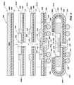
- FIG. 3Illustrated in FIG. 3 is one embodiment of a method of forming a BOC package.
- FIG. 3 , segment 301 aillustrates a precursor structure 300 comprising a metal or alloy core base 306 p , a precursor structure for the formation of a core member 306 , disposed on a dielectric layer 326 , which, in turn, is disposed on a thinner conductive layer C.
- Metal or alloy core base 306 pmay be formed, by way of example only, by electroplating or electroless plating and may be of, for example, 500 ⁇ m thickness.
- Metal or alloy core base 306 pmay be adhered to the dielectric layer 326 by a bonding agent (not shown), such as an epoxy, adhesive, adhesive tape, among other methods known in the art.
- the bonding agentmay be applied to the core base 306 p , the dielectric layer 326 , or both.
- a flexible dielectric materialmay be a polyimide film or tape.
- dielectric layer 326may be disposed on metal or alloy core base 306 p in flowable form, such as with a spin-on technique (not shown).
- Conductive layer Cis a precursor structure to conductive traces 328 that terminate at terminal pads 330 ( FIG. 3 , segments 301 d and 301 e ).
- Conductive traces 328may be formed by the aforementioned masking, patterning and etching after conductive layer C is applied or blanket-deposited onto dielectric layer 326 , or preformed and applied to dielectric layer 326 .
- conductive traces 328comprise conductive paths suitably formed and may be configured of any suitable material.
- Cavity 308which may form a recess 108 for receiving a semiconductor die 104 , as seen in FIG. 1 , may be formed in the core base 306 p by mechanical techniques, such as milling or chemical techniques, such as a masking, patterning and chemical (wet) etching process, or other such methods of forming cavities in metals that are known in the art.
- the depth of the cavity 308may be substantially the same as or greater than the height of a semiconductor die 104 to be disposed therewithin, although a cavity 308 having a depth less than the height of the semiconductor die 104 falls within the scope of the invention.
- An aperture or trench 309may be formed through core base 306 p and dielectric layer 326 from the bottom of cavity 308 in the form of at least one slot or groove.
- the size and shape of the at least one slot or groovemay be selected to provide access therethrough to bond pads of a semiconductor die disposed active surface down in cavity 308 and to provide sufficient clearance for a capillary of automated wire bonding equipment to join bond pads (not shown) on the semiconductor die with conductive traces 328 .
- the trench 309may be formed by mechanical techniques, such as drilling, chemical techniques, such as a masking, patterning and (wet) chemical etching process, or other such methods of forming cavities that are known in the art.
- Flanges 306 fflanking the central portion of core base 306 p and spaced from cavity 308 , may also be formed in the core base 306 p by thinning using mechanical techniques such as milling, chemical techniques, such as a masking, patterning and chemical (wet) etching process, or other such methods of reducing a thickness of a metal that are known in the art, the resulting structure now comprising core member 306 , corresponding to core member 106 of FIG. 1 .
- Flanges 306 fcorrespond to flange members 106 f of the core member 106 as seen in FIG. 1 .
- the volume of core base 306 p removed in the process to form the flanges 306 fmay be substantially sufficient to ensure the flanges 306 f have the requisite ductility needed to plastically fold a portion of each flange 306 f back toward the central portion of core member 306 , as discussed below.
- a dielectric, passivating layer 324may be disposed on the floor of cavity 308 of core member 306 and, optionally, over the walls of cavity 308 and the exposed portions of the dielectric layer 326 in the area of the walls of trench 309 .
- the dielectric layer 324may be applied by a chemical vapor deposition (CVD) process, stereolithographic process, spray process, or other suitable methods known in the art. If only disposed on the floor of cavity 308 , dielectric layer 324 may comprise a preformed dielectric tape or film, as previously mentioned.
- Segment 301 d of FIG. 3illustrates positioning a semiconductor die 104 within the cavity 308 of core member 306 .
- a bonding agentsuch as an epoxy, thermoset or thermoplastic adhesive, heat or light curable polymer, adhesive coated tape, or the like, may be applied to the floor of cavity 308 over the dielectric layer 324 to secure semiconductor die 104 by its active surface with bond pads 110 aligned with trench 309 , unless dielectric layer 324 is already adhesive in nature.
- the bonding agentmay be applied to the semiconductor die 104 in the form of, for example, LOC (Leads On Chip) adhesive coated tape segments, and used to form dielectric layer 324 .
- Semiconductor die 104may be positioned within the cavity 308 by a pick and place apparatus using, for example, a vacuum quill, or other by another suitable technique known in the art.
- a wire bonding processmay be used to form or connect conductive elements 332 , joining at least some of the bond pads 110 on the semiconductor die 104 through the trench 309 to proximate ends of the conductive traces 328 disposed on the dielectric layer 326 .
- conductive interconnectsin the form of discrete conductive elements 334 , corresponding to discrete conductive elements 134 of FIG. 1 .
- the discrete conductive elements 334may be formed or disposed on enlarged areas 328 ′ of conductive traces 328 disposed on the dielectric layer 326 and provide, in conjunction with the conductive traces 328 and conductive elements 332 , external electrical communication for the semiconductor die 104 .
- a dielectric encapsulant 314such as an underfill compound, may be dispensed within the cavity 308 to protect the back side and sides of semiconductor die 104 .
- Trench 309may be filled and conductive elements 332 covered with another dielectric encapsulant 333 , such as a silicon-filled thermoplastic resin, in a transfer molding operation.
- dielectric encapsulant 333such as a silicon-filled thermoplastic resin
- stereolithographic techniques using a photopolymermay be employed, or pot molding of a resin, or glob top encapsulation using a silicone. Encapsulation may be effected prior to, or after, formation or disposition of discrete conductive elements 334 on conductive traces 328 .
- Segment 301 e of FIG. 3illustrates a completed semiconductor device assembly after the flanges 306 f of the core member 306 have been folded over the top of the core member 306 to locations proximate cavity 308 , resting and in contact with unthinned portions of core member 306 .
- Voids 320are formed between folded-over flanges 306 f and the central portion of core member 306 .
- Dashed vertical lines 336visible in segment 301 d of FIG. 3 , indicate the approximate location of the fold, it being understood that the length of flanges 306 f as depicted are not to scale.
- the folding processis a simple mechanical process, and effected using conventional trim-and-form equipment by applying a bending force at or substantially near the distal end of each flange 306 f , as known in the art.
- a bending forcethat is greater than the yield strength of each flange 306 f in the fold area, the flange 306 f may be caused to remain in its folded position without the use of a bonding agent.
- a bonding agent(not shown), such as epoxy, or other adhesive as known in the art, may be applied to a portion of the upper surface of the core member 306 , the surface of the flanges 306 f , or both, prior to the folding process.
- the bonding agentmay provide additional adhesion to prevent the flanges 306 f from moving away from the upper surface of the core member 306 .
- spot weldingmay be used to secure flanges 306 f to the central portion of core member 306 .
- Segment 401 aillustrates a precursor structure 400 including a metal or metal alloy core base 406 p disposed over a dielectric layer 426 , which, in turn, is disposed over a thinner conductive layer C.
- Metal or alloy core base 406 pis a precursor structure used to form a core member 406 and may be formed, by way of example only, by electroplating or electroless plating and may be of, for example, 500 ⁇ m thickness.
- Metal or alloy core base 406 pmay be adhered to the dielectric layer 426 by a bonding agent (not shown), such as an epoxy, adhesive, adhesive tape, among other methods known in the art.
- the bonding agentmay be applied to the core base 406 p , the dielectric layer 426 , or both.
- a flexible dielectric materialmay be a polyimide film or tape.
- dielectric layer 426may be disposed on metal or alloy base 406 p in flowable form, such as with a spin-on technique.
- Conductive layer Cis a precursor structure used to form conductive traces 428 that terminate at terminal pads 430 , which may be formed by the aforementioned masking, patterning and etching after conductive layer C is applied or blanket-deposited onto dielectric layer 426 . Alternatively, conductive traces 428 may be preformed and applied to dielectric layer 426 .
- Cavity 408which may form a recess 208 for receiving a semiconductor die 204 , as seen in FIG. 2 , may be formed in the core base 406 p by mechanical techniques, such as milling, chemical techniques, such as a masking, patterning and chemical (wet) etching process, or other suitable method of forming cavities in metals, as known in the art.
- the depth of the cavity 408may be substantially the same as or greater than the height of a semiconductor die 204 to be disposed therewithin, although a cavity having a depth less than the height of the semiconductor die 204 falls within the scope of the invention.
- Cavity 408may stop on dielectric layer 426 , after which apertures 426 a are formed in dielectric layer 426 adjacent the intended location of a semiconductor die 204 , and through which conductive elements 432 may be subsequently extended between bond pads 210 of a semiconductor die 204 and the upper surfaces of conductive traces 428 exposed through apertures 426 a . If cavity 408 does not stop on dielectric layer 426 but stops instead on conductive layer C, an optional act as described with reference to segment 401 c of FIG. 4 may be performed.
- Flanges 406 fmay also be formed in core base 406 p by mechanical techniques, such as milling, chemical techniques, such as a masking, patterning and chemical etching process, or other suitable methods of reducing a thickness of a metal that are known in the art.
- the volume of core base 406 p removed in the process to form the flanges 406 fmay be substantially sufficient to ensure that the flanges 406 f have the requisite ductility needed to plastically fold a portion of each flange 406 f back toward the central portion of core base 406 p , as discussed below.
- Flanges 406 fflanking the central portion of core base 406 p and spaced from cavity 408 , may also be formed in the core base 406 p by thinning using mechanical techniques, such as milling, chemical techniques, such as a masking, patterning and chemical (wet) etching process, or other such methods of reducing a thickness of a metal that are known in the art, the resulting structure now comprising core member 406 , corresponding to core member 206 of FIG. 2 .
- Flanges 406 fcorrespond to flange members 206 f of the core member 206 as seen in FIG. 2 .
- the volume of core base 406 p removed in the process to form the flanges 406 fmay be substantially sufficient to ensure the flanges 406 f have the requisite ductility needed to plastically fold a portion of each flange 406 f back toward the central portion of core member 406 , as discussed below.
- Segment 401 c of FIG. 4illustrates another, optional intermediate act in the manufacturing process, if dielectric layer 426 is removed during formation of cavity 408 .
- a dielectric, passivating layer 424may be disposed on the floor of cavity 408 of core member 406 and, optionally, over the walls of cavity 408 .
- the dielectric layer 424may be applied by a chemical vapor deposition (CVD) process, stereolithographic process using a dielectric photopolymer material, spray process, or other suitable methods known in the art. If only disposed on the floor of cavity 408 , dielectric layer 424 may comprise a preformed dielectric tape or film, as previously mentioned.
- the dielectric layer 424electrically isolates a semiconductor die 204 (see segment 401 d of FIG. 4 ) placed thereon from conductive traces 428 .
- Apertures 426 amay be formed, using conventional etching techniques, through dielectric layer 424 for extending conductive elements 432 (see segments 401 d , 401 e of FIG. 4 ) from semiconductor die 204 to the upper sides of conductive traces 428 . If a preformed dielectric tape or film is employed for dielectric layer 424 , apertures 426 a may be preformed therein.
- the apertures 426 amay be formed in situ during activation or disposition of the photopolymer, depending on the specific stereolithographic technique employed.
- conductive layer Cis configured with a die paddle under cavity 408 and semiconductor die 204 electrically connected thereto for ground or bias purposes
- an aperture (not shown) for electrically connecting the back side of semiconductor die 204may be provided in dielectric layer 424 or, if dielectric layer 426 has not been removed, in dielectric layer 426 .
- a conductive or conductor-filled epoxy paste, or a solder pastemay be used to effect a physical and electrical connection with the back side of semiconductor die 204 .
- Segment 401 d of FIG. 4illustrates positioning a semiconductor die 204 within the cavity 408 of core member 406 .
- a bonding agentsuch as an epoxy, thermoset or thermoplastic adhesive, heat or light curable polymer, adhesive coated tape, or the like, may be applied to the floor of cavity 408 over the dielectric layer 426 to secure semiconductor die 204 by its back side with peripheral bond pads 210 proximate apertures 426 a in dielectric layer 426 , unless dielectric layer 426 is already adhesive in nature.
- the bonding agentmay be applied to the semiconductor die 204 in the form of, for example, LOC (Leads On Chip) adhesive coated tape segments.
- Semiconductor die 204may be positioned within the cavity 408 by a pick and place apparatus using, for example, a vacuum quill, or other by another suitable technique known in the art.
- a wire bonding processmay be used to form or connect conductive elements 432 , joining at least some of the bond pads 210 on the semiconductor die 204 through the apertures 426 a in dielectric layer 426 to proximate ends of the conductive traces 428 disposed on the dielectric layer 426 .
- conductive interconnectsin the form of discrete conductive elements 434 , corresponding to discrete conductive elements 234 of FIG. 2 and which, as shown in FIG. 2 , may be of various configurations.
- the discrete conductive elements 434may be formed or disposed on enlarged areas 428 ′ of conductive traces 428 disposed on the dielectric layer 426 and provide, in conjunction with the conductive traces 428 and conductive elements 432 , external electrical communication for the semiconductor die 204 .
- a dielectric encapsulant 414such as an underfill compound, may be dispensed within the cavity 408 to protect the back side and sides of semiconductor die 204 .
- stereolithographic techniques using a photopolymermay be employed, or pot molding of a resin, or glob top encapsulation using a silicone. Encapsulation may be effected prior to, or after, formation or disposition of discrete conductive elements 434 on conductive traces 428 .
- Segment 401 e of FIG. 4illustrates a completed semiconductor device assembly after the flanges 406 f of the core member 406 have been folded over the top of the core member 406 to locations proximate cavity 408 , resting and in contact with unthinned portions of core member 406 .
- Voids 420are formed between fold-over flanges 406 f and the central portion of core member 406 .
- Dashed vertical lines 436visible in segment 401 d of FIG. 4 , indicate the approximate location of the fold, it being understood that the length of flanges 406 f as depicted are not to scale.
- the folding processis a simple mechanical process, and effected using conventional trim-and-form equipment by applying a bending force at or substantially near the distal end of each flange 406 f , as known in the art.
- a bending forcethat is greater than the yield strength of each flange 406 f in the fold area, the flange 406 f may be caused to remain in its folded position without the use of a bonding agent.
- a bonding agent(not shown), such as epoxy, or other adhesive as known in the art, may be applied to a portion of the upper surface of the core member 406 , the surface of the flanges 406 f , or both, prior to the folding process.
- the bonding agentmay provide additional adhesion to prevent the flanges 406 f from moving away from the upper surface of the core member 406 .
- spot weldingmay be used to secure flanges 406 f to the central portion of core member 406 .
- FIG. 5 of the drawingsdepicts, in schematic block form, an embodiment of a system 500 including at least one semiconductor device assembly according to one or more embodiments of the present invention.
- System 500may comprise, by way of nonlimiting example only, a personal computer, a server, a cell phone, a personal digital assistant (PDA), a camera, or any other system comprising a processor 502 and memory 508 and, optionally, an input device 504 and an output device 506 .
- PDApersonal digital assistant
Landscapes
- Engineering & Computer Science (AREA)
- Microelectronics & Electronic Packaging (AREA)
- Power Engineering (AREA)
- General Physics & Mathematics (AREA)
- Computer Hardware Design (AREA)
- Condensed Matter Physics & Semiconductors (AREA)
- Physics & Mathematics (AREA)
- Chemical & Material Sciences (AREA)
- Materials Engineering (AREA)
- Ceramic Engineering (AREA)
- Cooling Or The Like Of Semiconductors Or Solid State Devices (AREA)
- Fixed Capacitors And Capacitor Manufacturing Machines (AREA)
- Lead Frames For Integrated Circuits (AREA)
- Structures Or Materials For Encapsulating Or Coating Semiconductor Devices Or Solid State Devices (AREA)
- Structures For Mounting Electric Components On Printed Circuit Boards (AREA)
Abstract
Description
Claims (30)
Priority Applications (1)
| Application Number | Priority Date | Filing Date | Title |
|---|---|---|---|
| US12/201,222US8115112B2 (en) | 2006-08-28 | 2008-08-29 | Interposer substrates and semiconductor device assemblies and electronic systems including such interposer substrates |
Applications Claiming Priority (2)
| Application Number | Priority Date | Filing Date | Title |
|---|---|---|---|
| US11/511,184US7425758B2 (en) | 2006-08-28 | 2006-08-28 | Metal core foldover package structures |
| US12/201,222US8115112B2 (en) | 2006-08-28 | 2008-08-29 | Interposer substrates and semiconductor device assemblies and electronic systems including such interposer substrates |
Related Parent Applications (1)
| Application Number | Title | Priority Date | Filing Date |
|---|---|---|---|
| US11/511,184ContinuationUS7425758B2 (en) | 2006-08-28 | 2006-08-28 | Metal core foldover package structures |
Publications (2)
| Publication Number | Publication Date |
|---|---|
| US20080316728A1 US20080316728A1 (en) | 2008-12-25 |
| US8115112B2true US8115112B2 (en) | 2012-02-14 |
Family
ID=39112594
Family Applications (3)
| Application Number | Title | Priority Date | Filing Date |
|---|---|---|---|
| US11/511,184ActiveUS7425758B2 (en) | 2006-08-28 | 2006-08-28 | Metal core foldover package structures |
| US12/180,880Active2027-05-12US7915077B2 (en) | 2006-08-28 | 2008-07-28 | Methods of making metal core foldover package structures |
| US12/201,222Active2028-01-17US8115112B2 (en) | 2006-08-28 | 2008-08-29 | Interposer substrates and semiconductor device assemblies and electronic systems including such interposer substrates |
Family Applications Before (2)
| Application Number | Title | Priority Date | Filing Date |
|---|---|---|---|
| US11/511,184ActiveUS7425758B2 (en) | 2006-08-28 | 2006-08-28 | Metal core foldover package structures |
| US12/180,880Active2027-05-12US7915077B2 (en) | 2006-08-28 | 2008-07-28 | Methods of making metal core foldover package structures |
Country Status (4)
| Country | Link |
|---|---|
| US (3) | US7425758B2 (en) |
| SG (1) | SG141286A1 (en) |
| TW (1) | TWI343105B (en) |
| WO (1) | WO2008027746A2 (en) |
Cited By (15)
| Publication number | Priority date | Publication date | Assignee | Title |
|---|---|---|---|---|
| US20110156269A1 (en)* | 2009-12-31 | 2011-06-30 | Hynix Semiconductor Inc. | Semiconductor package and stack semiconductor package having the same |
| US20120241936A1 (en)* | 2011-03-21 | 2012-09-27 | Kim Jingwan | Integrated circuit packaging system with package-on-package and method of manufacture thereof |
| US20130140062A1 (en)* | 2011-12-05 | 2013-06-06 | Kuang-Yao Chang | Circuit board structure and method for manufacturing the same |
| US20130182394A1 (en)* | 2012-01-13 | 2013-07-18 | Tyco Electronics Corporation | Electronic module packages and assemblies for electrical systems |
| US20130271924A1 (en)* | 2012-04-13 | 2013-10-17 | Quanta Computer Inc. | System in package assembly |
| US20140160684A1 (en)* | 2012-12-06 | 2014-06-12 | Apple Inc. | Cooling for electronic components |
| US9082031B2 (en) | 2012-09-25 | 2015-07-14 | Honeywell International, Inc. | Package-on-package based integrated circuit chip imager |
| US9223167B2 (en) | 2013-06-26 | 2015-12-29 | Apple Inc. | Liquid crystal switching barrier thermal control |
| US20160079213A1 (en)* | 2010-01-20 | 2016-03-17 | Samsung Electronics Co., Ltd. | Stacked semiconductor package |
| US9389029B2 (en) | 2013-09-30 | 2016-07-12 | Apple Inc. | Heat transfer structure |
| US20170055349A1 (en)* | 2015-08-23 | 2017-02-23 | Unimicron Technology Corp. | Package structure and manufacturing method thereof |
| US9674986B2 (en) | 2015-08-03 | 2017-06-06 | Apple Inc. | Parallel heat spreader |
| US9691694B2 (en) | 2015-02-18 | 2017-06-27 | Qualcomm Incorporated | Substrate comprising stacks of interconnects, interconnect on solder resist layer and interconnect on side portion of substrate |
| US20180005993A1 (en)* | 2016-06-30 | 2018-01-04 | Winbond Electronics Corp. | Package and packaging process of a semiconductor device |
| US12301744B2 (en) | 2022-01-10 | 2025-05-13 | Apple Inc. | Handheld electronic device |
Families Citing this family (80)
| Publication number | Priority date | Publication date | Assignee | Title |
|---|---|---|---|---|
| US6856009B2 (en) | 2003-03-11 | 2005-02-15 | Micron Technology, Inc. | Techniques for packaging multiple device components |
| CN1868056A (en)* | 2003-10-15 | 2006-11-22 | 皇家飞利浦电子股份有限公司 | Device, system and electric element |
| KR101313391B1 (en) | 2004-11-03 | 2013-10-01 | 테세라, 인코포레이티드 | Stacked packaging improvements |
| US7767543B2 (en)* | 2005-09-06 | 2010-08-03 | Semiconductor Energy Laboratory Co., Ltd. | Method for manufacturing a micro-electro-mechanical device with a folded substrate |
| US8058101B2 (en) | 2005-12-23 | 2011-11-15 | Tessera, Inc. | Microelectronic packages and methods therefor |
| KR100836663B1 (en)* | 2006-02-16 | 2008-06-10 | 삼성전기주식회사 | Cavity formed package-on package and method for manufacturing same |
| JP4955648B2 (en)* | 2006-03-07 | 2012-06-20 | 日本電気株式会社 | Electronic device packages, modules, and electronic equipment |
| US7888185B2 (en)* | 2006-08-17 | 2011-02-15 | Micron Technology, Inc. | Semiconductor device assemblies and systems including at least one conductive pathway extending around a side of at least one semiconductor device |
| US7425758B2 (en)* | 2006-08-28 | 2008-09-16 | Micron Technology, Inc. | Metal core foldover package structures |
| US7622811B2 (en)* | 2006-09-14 | 2009-11-24 | Stats Chippac, Inc. | Semiconductor assembly with component attached on die back side |
| US8252615B2 (en) | 2006-12-22 | 2012-08-28 | Stats Chippac Ltd. | Integrated circuit package system employing mold flash prevention technology |
| US7928582B2 (en)* | 2007-03-09 | 2011-04-19 | Micron Technology, Inc. | Microelectronic workpieces and methods for manufacturing microelectronic devices using such workpieces |
| US8852986B2 (en)* | 2007-05-16 | 2014-10-07 | Stats Chippac Ltd. | Integrated circuit package system employing resilient member mold system technology |
| US20090016036A1 (en)* | 2007-07-13 | 2009-01-15 | Wong Shaw Fong | Conductor reinforcement for circuit boards |
| US7928550B2 (en)* | 2007-11-08 | 2011-04-19 | Texas Instruments Incorporated | Flexible interposer for stacking semiconductor chips and connecting same to substrate |
| US20090166065A1 (en)* | 2008-01-02 | 2009-07-02 | Clayton James E | Thin multi-chip flex module |
| JP5012612B2 (en)* | 2008-03-26 | 2012-08-29 | 日本電気株式会社 | Semiconductor device mounting structure and electronic device using the mounting structure |
| US7786568B2 (en)* | 2008-09-30 | 2010-08-31 | Powertech Technology Inc. | Window BGA semiconductor package |
| US9059174B2 (en)* | 2008-11-05 | 2015-06-16 | Stmicroelectronics, Inc. | Method to reduce metal fuse thickness without extra mask |
| TWI501380B (en)* | 2010-01-29 | 2015-09-21 | Nat Chip Implementation Ct Nat Applied Res Lab | Three-dimensional soc structure stacking by multiple chip modules |
| KR20110101410A (en)* | 2010-03-08 | 2011-09-16 | 삼성전자주식회사 | Package on package |
| JP2013529850A (en)* | 2010-07-05 | 2013-07-22 | モサイド・テクノロジーズ・インコーポレーテッド | Multi-chip package with thermal frame and assembly method |
| US9159708B2 (en) | 2010-07-19 | 2015-10-13 | Tessera, Inc. | Stackable molded microelectronic packages with area array unit connectors |
| US8482111B2 (en) | 2010-07-19 | 2013-07-09 | Tessera, Inc. | Stackable molded microelectronic packages |
| KR101075241B1 (en) | 2010-11-15 | 2011-11-01 | 테세라, 인코포레이티드 | Microelectronic package with terminals in dielectric member |
| US20120146206A1 (en) | 2010-12-13 | 2012-06-14 | Tessera Research Llc | Pin attachment |
| US8618659B2 (en) | 2011-05-03 | 2013-12-31 | Tessera, Inc. | Package-on-package assembly with wire bonds to encapsulation surface |
| KR101128063B1 (en) | 2011-05-03 | 2012-04-23 | 테세라, 인코포레이티드 | Package-on-package assembly with wire bonds to encapsulation surface |
| US10163744B2 (en)* | 2011-09-07 | 2018-12-25 | STATS ChipPAC Pte. Ltd. | Semiconductor device and method of forming a low profile dual-purpose shield and heat-dissipation structure |
| US8836136B2 (en) | 2011-10-17 | 2014-09-16 | Invensas Corporation | Package-on-package assembly with wire bond vias |
| CN102522380B (en)* | 2011-12-21 | 2014-12-03 | 华为技术有限公司 | PoP packaging structure |
| US8946757B2 (en) | 2012-02-17 | 2015-02-03 | Invensas Corporation | Heat spreading substrate with embedded interconnects |
| US9349706B2 (en) | 2012-02-24 | 2016-05-24 | Invensas Corporation | Method for package-on-package assembly with wire bonds to encapsulation surface |
| US8372741B1 (en) | 2012-02-24 | 2013-02-12 | Invensas Corporation | Method for package-on-package assembly with wire bonds to encapsulation surface |
| US8835228B2 (en) | 2012-05-22 | 2014-09-16 | Invensas Corporation | Substrate-less stackable package with wire-bond interconnect |
| US9391008B2 (en) | 2012-07-31 | 2016-07-12 | Invensas Corporation | Reconstituted wafer-level package DRAM |
| US9502390B2 (en) | 2012-08-03 | 2016-11-22 | Invensas Corporation | BVA interposer |
| US8975738B2 (en) | 2012-11-12 | 2015-03-10 | Invensas Corporation | Structure for microelectronic packaging with terminals on dielectric mass |
| US8878353B2 (en) | 2012-12-20 | 2014-11-04 | Invensas Corporation | Structure for microelectronic packaging with bond elements to encapsulation surface |
| US9136254B2 (en) | 2013-02-01 | 2015-09-15 | Invensas Corporation | Microelectronic package having wire bond vias and stiffening layer |
| US10913653B2 (en)* | 2013-03-07 | 2021-02-09 | MCube Inc. | Method of fabricating MEMS devices using plasma etching and device therefor |
| US8883563B1 (en) | 2013-07-15 | 2014-11-11 | Invensas Corporation | Fabrication of microelectronic assemblies having stack terminals coupled by connectors extending through encapsulation |
| US9034696B2 (en) | 2013-07-15 | 2015-05-19 | Invensas Corporation | Microelectronic assemblies having reinforcing collars on connectors extending through encapsulation |
| US9023691B2 (en) | 2013-07-15 | 2015-05-05 | Invensas Corporation | Microelectronic assemblies with stack terminals coupled by connectors extending through encapsulation |
| US9167710B2 (en) | 2013-08-07 | 2015-10-20 | Invensas Corporation | Embedded packaging with preformed vias |
| US9685365B2 (en) | 2013-08-08 | 2017-06-20 | Invensas Corporation | Method of forming a wire bond having a free end |
| US20150076714A1 (en) | 2013-09-16 | 2015-03-19 | Invensas Corporation | Microelectronic element with bond elements to encapsulation surface |
| CN103560119B (en)* | 2013-11-05 | 2016-06-01 | 华进半导体封装先导技术研发中心有限公司 | For shielding three-dimension flexible substrate encapsulation structure and the making method of chip more |
| US9082753B2 (en) | 2013-11-12 | 2015-07-14 | Invensas Corporation | Severing bond wire by kinking and twisting |
| US9087815B2 (en) | 2013-11-12 | 2015-07-21 | Invensas Corporation | Off substrate kinking of bond wire |
| US9379074B2 (en) | 2013-11-22 | 2016-06-28 | Invensas Corporation | Die stacks with one or more bond via arrays of wire bond wires and with one or more arrays of bump interconnects |
| US9583456B2 (en) | 2013-11-22 | 2017-02-28 | Invensas Corporation | Multiple bond via arrays of different wire heights on a same substrate |
| US9263394B2 (en) | 2013-11-22 | 2016-02-16 | Invensas Corporation | Multiple bond via arrays of different wire heights on a same substrate |
| US9583411B2 (en) | 2014-01-17 | 2017-02-28 | Invensas Corporation | Fine pitch BVA using reconstituted wafer with area array accessible for testing |
| CN103871972A (en)* | 2014-03-31 | 2014-06-18 | 华为技术有限公司 | Flange, semiconductor power device and integrated circuit board |
| US9214454B2 (en) | 2014-03-31 | 2015-12-15 | Invensas Corporation | Batch process fabrication of package-on-package microelectronic assemblies |
| US10381326B2 (en) | 2014-05-28 | 2019-08-13 | Invensas Corporation | Structure and method for integrated circuits packaging with increased density |
| US9646917B2 (en) | 2014-05-29 | 2017-05-09 | Invensas Corporation | Low CTE component with wire bond interconnects |
| US9412714B2 (en) | 2014-05-30 | 2016-08-09 | Invensas Corporation | Wire bond support structure and microelectronic package including wire bonds therefrom |
| KR102243285B1 (en) | 2014-07-01 | 2021-04-23 | 삼성전자주식회사 | A semiconductor package |
| TW201608696A (en)* | 2014-08-28 | 2016-03-01 | 力晶科技股份有限公司 | Memory chip package module |
| US9735084B2 (en) | 2014-12-11 | 2017-08-15 | Invensas Corporation | Bond via array for thermal conductivity |
| US9888579B2 (en) | 2015-03-05 | 2018-02-06 | Invensas Corporation | Pressing of wire bond wire tips to provide bent-over tips |
| US9502372B1 (en) | 2015-04-30 | 2016-11-22 | Invensas Corporation | Wafer-level packaging using wire bond wires in place of a redistribution layer |
| US9761554B2 (en) | 2015-05-07 | 2017-09-12 | Invensas Corporation | Ball bonding metal wire bond wires to metal pads |
| KR20160132751A (en)* | 2015-05-11 | 2016-11-21 | 삼성전기주식회사 | Electronic component package and method of manufacturing the same |
| US10199337B2 (en) | 2015-05-11 | 2019-02-05 | Samsung Electro-Mechanics Co., Ltd. | Electronic component package and method of manufacturing the same |
| US9984979B2 (en) | 2015-05-11 | 2018-05-29 | Samsung Electro-Mechanics Co., Ltd. | Fan-out semiconductor package and method of manufacturing the same |
| US9490222B1 (en) | 2015-10-12 | 2016-11-08 | Invensas Corporation | Wire bond wires for interference shielding |
| US10490528B2 (en) | 2015-10-12 | 2019-11-26 | Invensas Corporation | Embedded wire bond wires |
| US10332854B2 (en) | 2015-10-23 | 2019-06-25 | Invensas Corporation | Anchoring structure of fine pitch bva |
| US10181457B2 (en) | 2015-10-26 | 2019-01-15 | Invensas Corporation | Microelectronic package for wafer-level chip scale packaging with fan-out |
| US10043779B2 (en) | 2015-11-17 | 2018-08-07 | Invensas Corporation | Packaged microelectronic device for a package-on-package device |
| US9659848B1 (en) | 2015-11-18 | 2017-05-23 | Invensas Corporation | Stiffened wires for offset BVA |
| US9984992B2 (en) | 2015-12-30 | 2018-05-29 | Invensas Corporation | Embedded wire bond wires for vertical integration with separate surface mount and wire bond mounting surfaces |
| US9935075B2 (en) | 2016-07-29 | 2018-04-03 | Invensas Corporation | Wire bonding method and apparatus for electromagnetic interference shielding |
| US10299368B2 (en) | 2016-12-21 | 2019-05-21 | Invensas Corporation | Surface integrated waveguides and circuit structures therefor |
| JP2018170333A (en)* | 2017-03-29 | 2018-11-01 | 株式会社東芝 | Semiconductor device and method of manufacturing the same |
| US11508587B2 (en) | 2017-12-29 | 2022-11-22 | Intel Corporation | Microelectronic assemblies |
| JP6984949B2 (en)* | 2019-08-28 | 2021-12-22 | Necプラットフォームズ株式会社 | Manufacturing methods for semiconductor devices, electronic devices and semiconductor devices |
Citations (54)
| Publication number | Priority date | Publication date | Assignee | Title |
|---|---|---|---|---|
| US5151769A (en) | 1991-04-04 | 1992-09-29 | General Electric Company | Optically patterned RF shield for an integrated circuit chip for analog and/or digital operation at microwave frequencies |
| US5347159A (en) | 1990-09-24 | 1994-09-13 | Tessera, Inc. | Semiconductor chip assemblies with face-up mounting and rear-surface connection to substrate |
| US5386341A (en) | 1993-11-01 | 1995-01-31 | Motorola, Inc. | Flexible substrate folded in a U-shape with a rigidizer plate located in the notch of the U-shape |
| US5394303A (en) | 1992-09-11 | 1995-02-28 | Kabushiki Kaisha Toshiba | Semiconductor device |
| US5448511A (en) | 1994-06-01 | 1995-09-05 | Storage Technology Corporation | Memory stack with an integrated interconnect and mounting structure |
| TW260792B (en) | 1993-11-25 | 1995-10-21 | Framatome & Cie | |
| US5552910A (en) | 1993-11-29 | 1996-09-03 | Sharp Kabushiki Kaisha | Liquid crystal display having zinc sulfide switching elements and method for producing the same |
| US5646446A (en) | 1995-12-22 | 1997-07-08 | Fairchild Space And Defense Corporation | Three-dimensional flexible assembly of integrated circuits |
| US5764484A (en)* | 1996-11-15 | 1998-06-09 | Olin Corporation | Ground ring for a metal electronic package |
| US5904496A (en) | 1997-01-24 | 1999-05-18 | Chipscale, Inc. | Wafer fabrication of inside-wrapped contacts for electronic devices |
| US5982030A (en) | 1998-02-27 | 1999-11-09 | Macintrye; Donald Malcom | Rigid package with low stress mounting of semiconductor die |
| US6028365A (en) | 1998-03-30 | 2000-02-22 | Micron Technology, Inc. | Integrated circuit package and method of fabrication |
| US6072238A (en)* | 1999-04-07 | 2000-06-06 | Motorola, Inc. | Semiconductor component |
| US6160705A (en)* | 1997-05-09 | 2000-12-12 | Texas Instruments Incorporated | Ball grid array package and method using enhanced power and ground distribution circuitry |
| US6172418B1 (en) | 1998-06-24 | 2001-01-09 | Nec Corporation | Semiconductor device and method for fabricating the same |
| US6208521B1 (en) | 1997-05-19 | 2001-03-27 | Nitto Denko Corporation | Film carrier and laminate type mounting structure using same |
| US6225688B1 (en) | 1997-12-11 | 2001-05-01 | Tessera, Inc. | Stacked microelectronic assembly and method therefor |
| US6287890B1 (en)* | 1999-10-18 | 2001-09-11 | Thin Film Module, Inc. | Low cost decal material used for packaging |
| US6291892B1 (en)* | 1998-04-02 | 2001-09-18 | Oki Electric Industry Co., Ltd | Semiconductor package that includes a shallow metal basin surrounded by an insulator frame |
| US6300679B1 (en) | 1998-06-01 | 2001-10-09 | Semiconductor Components Industries, Llc | Flexible substrate for packaging a semiconductor component |
| US20010054756A1 (en)* | 2000-06-21 | 2001-12-27 | Michio Horiuchi | Multi-layered semiconductor device and method for producing the same |
| US20020001178A1 (en)* | 1994-04-28 | 2002-01-03 | Makoto Iijima | Semiconductor device and method of forming the same. |
| US6365434B1 (en) | 2000-06-28 | 2002-04-02 | Micron Technology, Inc. | Method and apparatus for reduced flash encapsulation of microelectronic devices |
| US6376769B1 (en) | 1999-05-18 | 2002-04-23 | Amerasia International Technology, Inc. | High-density electronic package, and method for making same |
| US6486544B1 (en) | 1998-09-09 | 2002-11-26 | Seiko Epson Corporation | Semiconductor device and method manufacturing the same, circuit board, and electronic instrument |
| US6563223B2 (en) | 2000-08-22 | 2003-05-13 | Micron Technology, Inc. | Interconnection component for facilitating testing of packaged integrated circuits |
| US6576992B1 (en) | 2001-10-26 | 2003-06-10 | Staktek Group L.P. | Chip scale stacking system and method |
| US6600222B1 (en) | 2002-07-17 | 2003-07-29 | Intel Corporation | Stacked microelectronic packages |
| DE10227305A1 (en) | 2002-06-19 | 2003-09-04 | Siemens Dematic Ag | Electrical multiple layer component module used in polymer stud grid array technology comprises a second three-dimensional substrate arranged on first three-dimensional substrate with intermediate connections connected to contacts |
| US20030207501A1 (en)* | 2002-05-06 | 2003-11-06 | Schoenfeld Aaron M. | Semiconductor component with adjustment circuitry and method of fabrication |
| US20040000707A1 (en) | 2001-10-26 | 2004-01-01 | Staktek Group, L.P. | Modularized die stacking system and method |
| US6706553B2 (en)* | 2001-03-26 | 2004-03-16 | Intel Corporation | Dispensing process for fabrication of microelectronic packages |
| US20040115866A1 (en) | 2002-09-06 | 2004-06-17 | Tessera, Inc. | Methods of making microelectronic packages including folded substrates |
| US20040150088A1 (en)* | 2003-01-30 | 2004-08-05 | Micron Technology, Inc. | Semiconductor die package |
| US20040217471A1 (en)* | 2003-02-27 | 2004-11-04 | Tessera, Inc. | Component and assemblies with ends offset downwardly |
| US6833614B2 (en) | 2002-08-23 | 2004-12-21 | Shinko Electric Industries Co., Ltd. | Semiconductor package and semiconductor device |
| US20050009234A1 (en) | 2001-10-26 | 2005-01-13 | Staktek Group, L.P. | Stacked module systems and methods for CSP packages |
| US20050073846A1 (en) | 2001-09-27 | 2005-04-07 | Kenji Takine | Lightemitting device and method of manufacturing the same |
| US20050098873A1 (en) | 2003-09-15 | 2005-05-12 | Staktek Group L.P. | Stacked module systems and methods |
| US20050104205A1 (en)* | 2003-10-08 | 2005-05-19 | Chung-Cheng Wang | Substrate for electrical device and methods of manufacturing the same |
| US6914324B2 (en) | 2001-10-26 | 2005-07-05 | Staktek Group L.P. | Memory expansion and chip scale stacking system and method |
| US6919626B2 (en) | 1992-12-11 | 2005-07-19 | Staktek Group L.P. | High density integrated circuit module |
| US6940729B2 (en) | 2001-10-26 | 2005-09-06 | Staktek Group L.P. | Integrated circuit stacking system and method |
| US6956284B2 (en) | 2001-10-26 | 2005-10-18 | Staktek Group L.P. | Integrated circuit stacking system and method |
| US20050242423A1 (en)* | 2001-10-26 | 2005-11-03 | Staktek Group, L.P. | Stacked module systems and methods |
| US20060055038A1 (en) | 2004-09-10 | 2006-03-16 | Jinghui Mu | Tape ball grid array package with electromagnetic interference protection and method for fabricating the package |
| US7026708B2 (en) | 2001-10-26 | 2006-04-11 | Staktek Group L.P. | Low profile chip scale stacking system and method |
| US7053478B2 (en) | 2001-10-26 | 2006-05-30 | Staktek Group L.P. | Pitch change and chip scale stacking system |
| TWI260792B (en) | 2005-07-26 | 2006-08-21 | United Microelectronics Corp | Flip chip package with reduced thermal stress |
| US7309914B2 (en)* | 2005-01-20 | 2007-12-18 | Staktek Group L.P. | Inverted CSP stacking system and method |
| US20080048309A1 (en)* | 2006-08-28 | 2008-02-28 | Corisis David J | Metal core foldover package structures, systems including same and methods of fabrication |
| US7453155B2 (en) | 2005-04-08 | 2008-11-18 | Phoenix Precision Technology Corporation | Method for fabricating a flip chip package |
| US7563645B2 (en)* | 2003-07-17 | 2009-07-21 | Intel Corporation | Electronic package having a folded package substrate |
| US20100276799A1 (en) | 2009-05-04 | 2010-11-04 | Heng Stephen F | Semiconductor Chip Package with Stiffener Frame and Configured Lid |
- 2006
- 2006-08-28USUS11/511,184patent/US7425758B2/enactiveActive
- 2006-10-04SGSG200606927-2Apatent/SG141286A1/enunknown
- 2007
- 2007-08-20WOPCT/US2007/076286patent/WO2008027746A2/enactiveApplication Filing
- 2007-08-27TWTW096131721Apatent/TWI343105B/enactive
- 2008
- 2008-07-28USUS12/180,880patent/US7915077B2/enactiveActive
- 2008-08-29USUS12/201,222patent/US8115112B2/enactiveActive
Patent Citations (61)
| Publication number | Priority date | Publication date | Assignee | Title |
|---|---|---|---|---|
| US5347159A (en) | 1990-09-24 | 1994-09-13 | Tessera, Inc. | Semiconductor chip assemblies with face-up mounting and rear-surface connection to substrate |
| US5151769A (en) | 1991-04-04 | 1992-09-29 | General Electric Company | Optically patterned RF shield for an integrated circuit chip for analog and/or digital operation at microwave frequencies |
| US5394303A (en) | 1992-09-11 | 1995-02-28 | Kabushiki Kaisha Toshiba | Semiconductor device |
| US6919626B2 (en) | 1992-12-11 | 2005-07-19 | Staktek Group L.P. | High density integrated circuit module |
| US5386341A (en) | 1993-11-01 | 1995-01-31 | Motorola, Inc. | Flexible substrate folded in a U-shape with a rigidizer plate located in the notch of the U-shape |
| TW260792B (en) | 1993-11-25 | 1995-10-21 | Framatome & Cie | |
| US5552910A (en) | 1993-11-29 | 1996-09-03 | Sharp Kabushiki Kaisha | Liquid crystal display having zinc sulfide switching elements and method for producing the same |
| US20020001178A1 (en)* | 1994-04-28 | 2002-01-03 | Makoto Iijima | Semiconductor device and method of forming the same. |
| US5448511A (en) | 1994-06-01 | 1995-09-05 | Storage Technology Corporation | Memory stack with an integrated interconnect and mounting structure |
| US5646446A (en) | 1995-12-22 | 1997-07-08 | Fairchild Space And Defense Corporation | Three-dimensional flexible assembly of integrated circuits |
| US5776797A (en) | 1995-12-22 | 1998-07-07 | Fairchild Space And Defense Corporation | Three-dimensional flexible assembly of integrated circuits |
| US5764484A (en)* | 1996-11-15 | 1998-06-09 | Olin Corporation | Ground ring for a metal electronic package |
| US5904496A (en) | 1997-01-24 | 1999-05-18 | Chipscale, Inc. | Wafer fabrication of inside-wrapped contacts for electronic devices |
| US6160705A (en)* | 1997-05-09 | 2000-12-12 | Texas Instruments Incorporated | Ball grid array package and method using enhanced power and ground distribution circuitry |
| US6208521B1 (en) | 1997-05-19 | 2001-03-27 | Nitto Denko Corporation | Film carrier and laminate type mounting structure using same |
| US6225688B1 (en) | 1997-12-11 | 2001-05-01 | Tessera, Inc. | Stacked microelectronic assembly and method therefor |
| US5982030A (en) | 1998-02-27 | 1999-11-09 | Macintrye; Donald Malcom | Rigid package with low stress mounting of semiconductor die |
| US6028365A (en) | 1998-03-30 | 2000-02-22 | Micron Technology, Inc. | Integrated circuit package and method of fabrication |
| US6291892B1 (en)* | 1998-04-02 | 2001-09-18 | Oki Electric Industry Co., Ltd | Semiconductor package that includes a shallow metal basin surrounded by an insulator frame |
| US6300679B1 (en) | 1998-06-01 | 2001-10-09 | Semiconductor Components Industries, Llc | Flexible substrate for packaging a semiconductor component |
| US6172418B1 (en) | 1998-06-24 | 2001-01-09 | Nec Corporation | Semiconductor device and method for fabricating the same |
| US6486544B1 (en) | 1998-09-09 | 2002-11-26 | Seiko Epson Corporation | Semiconductor device and method manufacturing the same, circuit board, and electronic instrument |
| US6072238A (en)* | 1999-04-07 | 2000-06-06 | Motorola, Inc. | Semiconductor component |
| US6376769B1 (en) | 1999-05-18 | 2002-04-23 | Amerasia International Technology, Inc. | High-density electronic package, and method for making same |
| US6287890B1 (en)* | 1999-10-18 | 2001-09-11 | Thin Film Module, Inc. | Low cost decal material used for packaging |
| US6586846B2 (en)* | 1999-10-18 | 2003-07-01 | Thin Film Module, Inc. | Low cost decal material used for packaging |
| US20010054756A1 (en)* | 2000-06-21 | 2001-12-27 | Michio Horiuchi | Multi-layered semiconductor device and method for producing the same |
| US6365434B1 (en) | 2000-06-28 | 2002-04-02 | Micron Technology, Inc. | Method and apparatus for reduced flash encapsulation of microelectronic devices |
| US6563223B2 (en) | 2000-08-22 | 2003-05-13 | Micron Technology, Inc. | Interconnection component for facilitating testing of packaged integrated circuits |
| US6706553B2 (en)* | 2001-03-26 | 2004-03-16 | Intel Corporation | Dispensing process for fabrication of microelectronic packages |
| US20050073846A1 (en) | 2001-09-27 | 2005-04-07 | Kenji Takine | Lightemitting device and method of manufacturing the same |
| US6955945B2 (en) | 2001-10-26 | 2005-10-18 | Staktek Group L.P. | Memory expansion and chip scale stacking system and method |
| US7094632B2 (en) | 2001-10-26 | 2006-08-22 | Staktek Group L.P. | Low profile chip scale stacking system and method |
| US20040000707A1 (en) | 2001-10-26 | 2004-01-01 | Staktek Group, L.P. | Modularized die stacking system and method |
| US7053478B2 (en) | 2001-10-26 | 2006-05-30 | Staktek Group L.P. | Pitch change and chip scale stacking system |
| US7026708B2 (en) | 2001-10-26 | 2006-04-11 | Staktek Group L.P. | Low profile chip scale stacking system and method |
| US20050280135A1 (en) | 2001-10-26 | 2005-12-22 | Staktek Group L.P. | Stacking system and method |
| US20050242423A1 (en)* | 2001-10-26 | 2005-11-03 | Staktek Group, L.P. | Stacked module systems and methods |
| US20050009234A1 (en) | 2001-10-26 | 2005-01-13 | Staktek Group, L.P. | Stacked module systems and methods for CSP packages |
| US6956284B2 (en) | 2001-10-26 | 2005-10-18 | Staktek Group L.P. | Integrated circuit stacking system and method |
| US6576992B1 (en) | 2001-10-26 | 2003-06-10 | Staktek Group L.P. | Chip scale stacking system and method |
| US6940729B2 (en) | 2001-10-26 | 2005-09-06 | Staktek Group L.P. | Integrated circuit stacking system and method |
| US6914324B2 (en) | 2001-10-26 | 2005-07-05 | Staktek Group L.P. | Memory expansion and chip scale stacking system and method |
| US20030207501A1 (en)* | 2002-05-06 | 2003-11-06 | Schoenfeld Aaron M. | Semiconductor component with adjustment circuitry and method of fabrication |
| DE10227305A1 (en) | 2002-06-19 | 2003-09-04 | Siemens Dematic Ag | Electrical multiple layer component module used in polymer stud grid array technology comprises a second three-dimensional substrate arranged on first three-dimensional substrate with intermediate connections connected to contacts |
| US6600222B1 (en) | 2002-07-17 | 2003-07-29 | Intel Corporation | Stacked microelectronic packages |
| US6833614B2 (en) | 2002-08-23 | 2004-12-21 | Shinko Electric Industries Co., Ltd. | Semiconductor package and semiconductor device |
| US20040115866A1 (en) | 2002-09-06 | 2004-06-17 | Tessera, Inc. | Methods of making microelectronic packages including folded substrates |
| US20040150088A1 (en)* | 2003-01-30 | 2004-08-05 | Micron Technology, Inc. | Semiconductor die package |
| US20040217471A1 (en)* | 2003-02-27 | 2004-11-04 | Tessera, Inc. | Component and assemblies with ends offset downwardly |
| US7563645B2 (en)* | 2003-07-17 | 2009-07-21 | Intel Corporation | Electronic package having a folded package substrate |
| US20050098873A1 (en) | 2003-09-15 | 2005-05-12 | Staktek Group L.P. | Stacked module systems and methods |
| US20050104205A1 (en)* | 2003-10-08 | 2005-05-19 | Chung-Cheng Wang | Substrate for electrical device and methods of manufacturing the same |
| US20060055038A1 (en) | 2004-09-10 | 2006-03-16 | Jinghui Mu | Tape ball grid array package with electromagnetic interference protection and method for fabricating the package |
| US7309914B2 (en)* | 2005-01-20 | 2007-12-18 | Staktek Group L.P. | Inverted CSP stacking system and method |
| US7453155B2 (en) | 2005-04-08 | 2008-11-18 | Phoenix Precision Technology Corporation | Method for fabricating a flip chip package |
| TWI260792B (en) | 2005-07-26 | 2006-08-21 | United Microelectronics Corp | Flip chip package with reduced thermal stress |
| US20080048309A1 (en)* | 2006-08-28 | 2008-02-28 | Corisis David J | Metal core foldover package structures, systems including same and methods of fabrication |
| US7425758B2 (en)* | 2006-08-28 | 2008-09-16 | Micron Technology, Inc. | Metal core foldover package structures |
| US20080299709A1 (en)* | 2006-08-28 | 2008-12-04 | Micron Technology, Inc. | Metal core foldover package structures |
| US20100276799A1 (en) | 2009-05-04 | 2010-11-04 | Heng Stephen F | Semiconductor Chip Package with Stiffener Frame and Configured Lid |
Non-Patent Citations (4)
| Title |
|---|
| International Preliminary Report on Patentability dated Mar. 3, 2009 for International Application No. PCT/US2007/076286 (7 pages). |
| International Search Report dated Apr. 11, 2008, for International Application No. PCT/US2007/076286 (4 pages). |
| TW Search Report for TW Application No. 096131721 completed Nov. 27, 2010, 2 pages. |
| Written Opinion dated Apr. 11, 2008, for International Application No. PCT/US2007/076286 (5 pages). |
Cited By (22)
| Publication number | Priority date | Publication date | Assignee | Title |
|---|---|---|---|---|
| US20110156269A1 (en)* | 2009-12-31 | 2011-06-30 | Hynix Semiconductor Inc. | Semiconductor package and stack semiconductor package having the same |
| US20160079213A1 (en)* | 2010-01-20 | 2016-03-17 | Samsung Electronics Co., Ltd. | Stacked semiconductor package |
| US20120241936A1 (en)* | 2011-03-21 | 2012-09-27 | Kim Jingwan | Integrated circuit packaging system with package-on-package and method of manufacture thereof |
| US8432028B2 (en)* | 2011-03-21 | 2013-04-30 | Stats Chippac Ltd. | Integrated circuit packaging system with package-on-package and method of manufacture thereof |
| US20130140062A1 (en)* | 2011-12-05 | 2013-06-06 | Kuang-Yao Chang | Circuit board structure and method for manufacturing the same |
| US20130182394A1 (en)* | 2012-01-13 | 2013-07-18 | Tyco Electronics Corporation | Electronic module packages and assemblies for electrical systems |
| US8867231B2 (en)* | 2012-01-13 | 2014-10-21 | Tyco Electronics Corporation | Electronic module packages and assemblies for electrical systems |
| US20130271924A1 (en)* | 2012-04-13 | 2013-10-17 | Quanta Computer Inc. | System in package assembly |
| US9119320B2 (en)* | 2012-04-13 | 2015-08-25 | Quanta Computer Inc. | System in package assembly |
| US9430686B2 (en) | 2012-09-25 | 2016-08-30 | Honeywell International, Inc. | Package-on-package based integrated circuit chip imager |
| US9082031B2 (en) | 2012-09-25 | 2015-07-14 | Honeywell International, Inc. | Package-on-package based integrated circuit chip imager |
| US9125299B2 (en)* | 2012-12-06 | 2015-09-01 | Apple Inc. | Cooling for electronic components |
| US20140160684A1 (en)* | 2012-12-06 | 2014-06-12 | Apple Inc. | Cooling for electronic components |
| US9223167B2 (en) | 2013-06-26 | 2015-12-29 | Apple Inc. | Liquid crystal switching barrier thermal control |
| US9389029B2 (en) | 2013-09-30 | 2016-07-12 | Apple Inc. | Heat transfer structure |
| US9691694B2 (en) | 2015-02-18 | 2017-06-27 | Qualcomm Incorporated | Substrate comprising stacks of interconnects, interconnect on solder resist layer and interconnect on side portion of substrate |
| US9674986B2 (en) | 2015-08-03 | 2017-06-06 | Apple Inc. | Parallel heat spreader |
| US20170055349A1 (en)* | 2015-08-23 | 2017-02-23 | Unimicron Technology Corp. | Package structure and manufacturing method thereof |
| US9686866B2 (en)* | 2015-08-23 | 2017-06-20 | Unimicron Technology Corp. | Package structure and manufacturing method thereof |
| US20180005993A1 (en)* | 2016-06-30 | 2018-01-04 | Winbond Electronics Corp. | Package and packaging process of a semiconductor device |
| US9991232B2 (en)* | 2016-06-30 | 2018-06-05 | Winbond Electronics Corp. | Package and packaging process of a semiconductor device |
| US12301744B2 (en) | 2022-01-10 | 2025-05-13 | Apple Inc. | Handheld electronic device |
Also Published As
| Publication number | Publication date |
|---|---|
| US20080316728A1 (en) | 2008-12-25 |
| US7915077B2 (en) | 2011-03-29 |
| WO2008027746B1 (en) | 2008-07-31 |
| SG141286A1 (en) | 2008-04-28 |
| US7425758B2 (en) | 2008-09-16 |
| US20080048309A1 (en) | 2008-02-28 |
| TWI343105B (en) | 2011-06-01 |
| US20080299709A1 (en) | 2008-12-04 |
| WO2008027746A2 (en) | 2008-03-06 |
| WO2008027746A3 (en) | 2008-06-05 |
| TW200818435A (en) | 2008-04-16 |
Similar Documents
| Publication | Publication Date | Title |
|---|---|---|
| US8115112B2 (en) | Interposer substrates and semiconductor device assemblies and electronic systems including such interposer substrates | |
| US6369448B1 (en) | Vertically integrated flip chip semiconductor package | |
| US7198980B2 (en) | Methods for assembling multiple semiconductor devices | |
| US7915718B2 (en) | Apparatus for flip-chip packaging providing testing capability | |
| US7573136B2 (en) | Semiconductor device assemblies and packages including multiple semiconductor device components | |
| US8174105B2 (en) | Stacked semiconductor package having discrete components | |
| US6414381B1 (en) | Interposer for separating stacked semiconductor chips mounted on a multi-layer printed circuit board | |
| US7309913B2 (en) | Stacked semiconductor packages | |
| KR101407773B1 (en) | Apparatus for packaging semiconductor devices, packaged semiconductor components, methods of manufacturing apparatus for packaging semiconductor devices, and methods of manufacturing semiconductor components | |
| CN100499052C (en) | Planar grid array packaging device and manufacturing method thereof | |
| US8927332B2 (en) | Methods of manufacturing semiconductor device assemblies including face-to-face semiconductor dice | |
| US7554185B2 (en) | Flip chip and wire bond semiconductor package | |
| US20060194373A1 (en) | Methods for assembling semiconductor devices and interposers | |
| KR101166575B1 (en) | Semiconductor multi-package module having wire bond interconnection between stacked packages | |
| KR20050074961A (en) | Semiconductor stacked multi-package module having inverted second package | |
| US9917073B2 (en) | Reconstituted wafer-level package dram with conductive interconnects formed in encapsulant at periphery of the package | |
| US20080237833A1 (en) | Multi-chip semiconductor package structure | |
| JPWO2003012863A1 (en) | Semiconductor device and manufacturing method thereof | |
| US7235870B2 (en) | Microelectronic multi-chip module | |
| US20080237831A1 (en) | Multi-chip semiconductor package structure | |
| Kisiel et al. | Trends in assembling of advanced IC packages | |
| US20080237832A1 (en) | Multi-chip semiconductor package structure | |
| CN118352323A (en) | Semiconductor packaging |
Legal Events
| Date | Code | Title | Description |
|---|---|---|---|
| FEPP | Fee payment procedure | Free format text:PAYOR NUMBER ASSIGNED (ORIGINAL EVENT CODE: ASPN); ENTITY STATUS OF PATENT OWNER: LARGE ENTITY | |
| STCF | Information on status: patent grant | Free format text:PATENTED CASE | |
| CC | Certificate of correction | ||
| FPAY | Fee payment | Year of fee payment:4 | |
| AS | Assignment | Owner name:U.S. BANK NATIONAL ASSOCIATION, AS COLLATERAL AGENT, CALIFORNIA Free format text:SECURITY INTEREST;ASSIGNOR:MICRON TECHNOLOGY, INC.;REEL/FRAME:038669/0001 Effective date:20160426 Owner name:U.S. BANK NATIONAL ASSOCIATION, AS COLLATERAL AGEN Free format text:SECURITY INTEREST;ASSIGNOR:MICRON TECHNOLOGY, INC.;REEL/FRAME:038669/0001 Effective date:20160426 | |
| AS | Assignment | Owner name:MORGAN STANLEY SENIOR FUNDING, INC., AS COLLATERAL AGENT, MARYLAND Free format text:PATENT SECURITY AGREEMENT;ASSIGNOR:MICRON TECHNOLOGY, INC.;REEL/FRAME:038954/0001 Effective date:20160426 Owner name:MORGAN STANLEY SENIOR FUNDING, INC., AS COLLATERAL Free format text:PATENT SECURITY AGREEMENT;ASSIGNOR:MICRON TECHNOLOGY, INC.;REEL/FRAME:038954/0001 Effective date:20160426 | |
| AS | Assignment | Owner name:U.S. BANK NATIONAL ASSOCIATION, AS COLLATERAL AGENT, CALIFORNIA Free format text:CORRECTIVE ASSIGNMENT TO CORRECT THE REPLACE ERRONEOUSLY FILED PATENT #7358718 WITH THE CORRECT PATENT #7358178 PREVIOUSLY RECORDED ON REEL 038669 FRAME 0001. ASSIGNOR(S) HEREBY CONFIRMS THE SECURITY INTEREST;ASSIGNOR:MICRON TECHNOLOGY, INC.;REEL/FRAME:043079/0001 Effective date:20160426 Owner name:U.S. BANK NATIONAL ASSOCIATION, AS COLLATERAL AGEN Free format text:CORRECTIVE ASSIGNMENT TO CORRECT THE REPLACE ERRONEOUSLY FILED PATENT #7358718 WITH THE CORRECT PATENT #7358178 PREVIOUSLY RECORDED ON REEL 038669 FRAME 0001. ASSIGNOR(S) HEREBY CONFIRMS THE SECURITY INTEREST;ASSIGNOR:MICRON TECHNOLOGY, INC.;REEL/FRAME:043079/0001 Effective date:20160426 | |
| AS | Assignment | Owner name:JPMORGAN CHASE BANK, N.A., AS COLLATERAL AGENT, ILLINOIS Free format text:SECURITY INTEREST;ASSIGNORS:MICRON TECHNOLOGY, INC.;MICRON SEMICONDUCTOR PRODUCTS, INC.;REEL/FRAME:047540/0001 Effective date:20180703 Owner name:JPMORGAN CHASE BANK, N.A., AS COLLATERAL AGENT, IL Free format text:SECURITY INTEREST;ASSIGNORS:MICRON TECHNOLOGY, INC.;MICRON SEMICONDUCTOR PRODUCTS, INC.;REEL/FRAME:047540/0001 Effective date:20180703 | |
| AS | Assignment | Owner name:MICRON TECHNOLOGY, INC., IDAHO Free format text:RELEASE BY SECURED PARTY;ASSIGNOR:U.S. BANK NATIONAL ASSOCIATION, AS COLLATERAL AGENT;REEL/FRAME:047243/0001 Effective date:20180629 | |
| MAFP | Maintenance fee payment | Free format text:PAYMENT OF MAINTENANCE FEE, 8TH YEAR, LARGE ENTITY (ORIGINAL EVENT CODE: M1552); ENTITY STATUS OF PATENT OWNER: LARGE ENTITY Year of fee payment:8 | |
| AS | Assignment | Owner name:MICRON TECHNOLOGY, INC., IDAHO Free format text:RELEASE BY SECURED PARTY;ASSIGNOR:MORGAN STANLEY SENIOR FUNDING, INC., AS COLLATERAL AGENT;REEL/FRAME:050937/0001 Effective date:20190731 | |
| AS | Assignment | Owner name:MICRON TECHNOLOGY, INC., IDAHO Free format text:RELEASE BY SECURED PARTY;ASSIGNOR:JPMORGAN CHASE BANK, N.A., AS COLLATERAL AGENT;REEL/FRAME:051028/0001 Effective date:20190731 Owner name:MICRON SEMICONDUCTOR PRODUCTS, INC., IDAHO Free format text:RELEASE BY SECURED PARTY;ASSIGNOR:JPMORGAN CHASE BANK, N.A., AS COLLATERAL AGENT;REEL/FRAME:051028/0001 Effective date:20190731 | |
| MAFP | Maintenance fee payment | Free format text:PAYMENT OF MAINTENANCE FEE, 12TH YEAR, LARGE ENTITY (ORIGINAL EVENT CODE: M1553); ENTITY STATUS OF PATENT OWNER: LARGE ENTITY Year of fee payment:12 |