US8114300B2 - Multi-layer method for formation of registered arrays of cylindrical pores in polymer films - Google Patents
Multi-layer method for formation of registered arrays of cylindrical pores in polymer filmsDownload PDFInfo
- Publication number
- US8114300B2 US8114300B2US12/106,562US10656208AUS8114300B2US 8114300 B2US8114300 B2US 8114300B2US 10656208 AUS10656208 AUS 10656208AUS 8114300 B2US8114300 B2US 8114300B2
- Authority
- US
- United States
- Prior art keywords
- block copolymer
- copolymer material
- block
- trench
- substrate
- Prior art date
- Legal status (The legal status is an assumption and is not a legal conclusion. Google has not performed a legal analysis and makes no representation as to the accuracy of the status listed.)
- Active
Links
Images


Classifications
- B—PERFORMING OPERATIONS; TRANSPORTING
- B05—SPRAYING OR ATOMISING IN GENERAL; APPLYING FLUENT MATERIALS TO SURFACES, IN GENERAL
- B05D—PROCESSES FOR APPLYING FLUENT MATERIALS TO SURFACES, IN GENERAL
- B05D3/00—Pretreatment of surfaces to which liquids or other fluent materials are to be applied; After-treatment of applied coatings, e.g. intermediate treating of an applied coating preparatory to subsequent applications of liquids or other fluent materials
- B05D3/02—Pretreatment of surfaces to which liquids or other fluent materials are to be applied; After-treatment of applied coatings, e.g. intermediate treating of an applied coating preparatory to subsequent applications of liquids or other fluent materials by baking
- B05D3/0254—After-treatment
- B—PERFORMING OPERATIONS; TRANSPORTING
- B05—SPRAYING OR ATOMISING IN GENERAL; APPLYING FLUENT MATERIALS TO SURFACES, IN GENERAL
- B05D—PROCESSES FOR APPLYING FLUENT MATERIALS TO SURFACES, IN GENERAL
- B05D1/00—Processes for applying liquids or other fluent materials
- B05D1/34—Applying different liquids or other fluent materials simultaneously
- G—PHYSICS
- G03—PHOTOGRAPHY; CINEMATOGRAPHY; ANALOGOUS TECHNIQUES USING WAVES OTHER THAN OPTICAL WAVES; ELECTROGRAPHY; HOLOGRAPHY
- G03F—PHOTOMECHANICAL PRODUCTION OF TEXTURED OR PATTERNED SURFACES, e.g. FOR PRINTING, FOR PROCESSING OF SEMICONDUCTOR DEVICES; MATERIALS THEREFOR; ORIGINALS THEREFOR; APPARATUS SPECIALLY ADAPTED THEREFOR
- G03F7/00—Photomechanical, e.g. photolithographic, production of textured or patterned surfaces, e.g. printing surfaces; Materials therefor, e.g. comprising photoresists; Apparatus specially adapted therefor
- G03F7/0002—Lithographic processes using patterning methods other than those involving the exposure to radiation, e.g. by stamping
- B—PERFORMING OPERATIONS; TRANSPORTING
- B05—SPRAYING OR ATOMISING IN GENERAL; APPLYING FLUENT MATERIALS TO SURFACES, IN GENERAL
- B05D—PROCESSES FOR APPLYING FLUENT MATERIALS TO SURFACES, IN GENERAL
- B05D5/00—Processes for applying liquids or other fluent materials to surfaces to obtain special surface effects, finishes or structures
- B05D5/02—Processes for applying liquids or other fluent materials to surfaces to obtain special surface effects, finishes or structures to obtain a matt or rough surface
- Y—GENERAL TAGGING OF NEW TECHNOLOGICAL DEVELOPMENTS; GENERAL TAGGING OF CROSS-SECTIONAL TECHNOLOGIES SPANNING OVER SEVERAL SECTIONS OF THE IPC; TECHNICAL SUBJECTS COVERED BY FORMER USPC CROSS-REFERENCE ART COLLECTIONS [XRACs] AND DIGESTS
- Y10—TECHNICAL SUBJECTS COVERED BY FORMER USPC
- Y10S—TECHNICAL SUBJECTS COVERED BY FORMER USPC CROSS-REFERENCE ART COLLECTIONS [XRACs] AND DIGESTS
- Y10S438/00—Semiconductor device manufacturing: process
- Y10S438/942—Masking
- Y10S438/947—Subphotolithographic processing
- Y—GENERAL TAGGING OF NEW TECHNOLOGICAL DEVELOPMENTS; GENERAL TAGGING OF CROSS-SECTIONAL TECHNOLOGIES SPANNING OVER SEVERAL SECTIONS OF THE IPC; TECHNICAL SUBJECTS COVERED BY FORMER USPC CROSS-REFERENCE ART COLLECTIONS [XRACs] AND DIGESTS
- Y10—TECHNICAL SUBJECTS COVERED BY FORMER USPC
- Y10S—TECHNICAL SUBJECTS COVERED BY FORMER USPC CROSS-REFERENCE ART COLLECTIONS [XRACs] AND DIGESTS
- Y10S977/00—Nanotechnology
- Y10S977/84—Manufacture, treatment, or detection of nanostructure
- Y10S977/888—Shaping or removal of materials, e.g. etching
- Y—GENERAL TAGGING OF NEW TECHNOLOGICAL DEVELOPMENTS; GENERAL TAGGING OF CROSS-SECTIONAL TECHNOLOGIES SPANNING OVER SEVERAL SECTIONS OF THE IPC; TECHNICAL SUBJECTS COVERED BY FORMER USPC CROSS-REFERENCE ART COLLECTIONS [XRACs] AND DIGESTS
- Y10—TECHNICAL SUBJECTS COVERED BY FORMER USPC
- Y10S—TECHNICAL SUBJECTS COVERED BY FORMER USPC CROSS-REFERENCE ART COLLECTIONS [XRACs] AND DIGESTS
- Y10S977/00—Nanotechnology
- Y10S977/84—Manufacture, treatment, or detection of nanostructure
- Y10S977/895—Manufacture, treatment, or detection of nanostructure having step or means utilizing chemical property
- Y—GENERAL TAGGING OF NEW TECHNOLOGICAL DEVELOPMENTS; GENERAL TAGGING OF CROSS-SECTIONAL TECHNOLOGIES SPANNING OVER SEVERAL SECTIONS OF THE IPC; TECHNICAL SUBJECTS COVERED BY FORMER USPC CROSS-REFERENCE ART COLLECTIONS [XRACs] AND DIGESTS
- Y10—TECHNICAL SUBJECTS COVERED BY FORMER USPC
- Y10S—TECHNICAL SUBJECTS COVERED BY FORMER USPC CROSS-REFERENCE ART COLLECTIONS [XRACs] AND DIGESTS
- Y10S977/00—Nanotechnology
- Y10S977/84—Manufacture, treatment, or detection of nanostructure
- Y10S977/90—Manufacture, treatment, or detection of nanostructure having step or means utilizing mechanical or thermal property, e.g. pressure, heat
- Y—GENERAL TAGGING OF NEW TECHNOLOGICAL DEVELOPMENTS; GENERAL TAGGING OF CROSS-SECTIONAL TECHNOLOGIES SPANNING OVER SEVERAL SECTIONS OF THE IPC; TECHNICAL SUBJECTS COVERED BY FORMER USPC CROSS-REFERENCE ART COLLECTIONS [XRACs] AND DIGESTS
- Y10—TECHNICAL SUBJECTS COVERED BY FORMER USPC
- Y10T—TECHNICAL SUBJECTS COVERED BY FORMER US CLASSIFICATION
- Y10T428/00—Stock material or miscellaneous articles
- Y10T428/24—Structurally defined web or sheet [e.g., overall dimension, etc.]
- Y10T428/24174—Structurally defined web or sheet [e.g., overall dimension, etc.] including sheet or component perpendicular to plane of web or sheet
- Y10T428/24182—Inward from edge of web or sheet
- Y—GENERAL TAGGING OF NEW TECHNOLOGICAL DEVELOPMENTS; GENERAL TAGGING OF CROSS-SECTIONAL TECHNOLOGIES SPANNING OVER SEVERAL SECTIONS OF THE IPC; TECHNICAL SUBJECTS COVERED BY FORMER USPC CROSS-REFERENCE ART COLLECTIONS [XRACs] AND DIGESTS
- Y10—TECHNICAL SUBJECTS COVERED BY FORMER USPC
- Y10T—TECHNICAL SUBJECTS COVERED BY FORMER US CLASSIFICATION
- Y10T428/00—Stock material or miscellaneous articles
- Y10T428/24—Structurally defined web or sheet [e.g., overall dimension, etc.]
- Y10T428/24479—Structurally defined web or sheet [e.g., overall dimension, etc.] including variation in thickness
- Y10T428/24612—Composite web or sheet
- Y10T428/2462—Composite web or sheet with partial filling of valleys on outer surface
Definitions
- Embodiments of the inventionrelate to methods of fabricating thin films of self-assembling block copolymers, and devices resulting from those methods.
- diblock copolymersspontaneously assemble into periodic structures by microphase separation of the constituent polymer blocks after annealing, for example by thermal annealing above the glass transition temperature of the polymer or by solvent annealing, forming ordered domains at nanometer-scale dimensions.
- the film morphologyincluding the size and shape of the microphase-separated domains, can be controlled by the molecular weight and volume fraction of the AB blocks of a diblock copolymer to produce lamellar, cylindrical, or spherical morphologies, among others.
- a block copolymer filmwill microphase separate and self-assemble into a periodic spherical domains with spheres of polymer B surrounded by a matrix of polymer A.
- the diblock copolymerFor ratios of the two blocks between about 60:40 and 80:20, the diblock copolymer assembles into a periodic hexagonal close-packed or honeycomb array of cylinders of polymer B within a matrix of polymer A. For ratios between about 50:50 and 60:40, lamellar domains or alternating stripes of the blocks are formed. Domain size typically ranges from 5-50 nm.
- the self-assembled filmsare further processed to selectively remove one of the blocks, leaving the other polymer block as an etch mask on the substrate.
- the polymer block that is removeddoes not extend completely through the film and requires an additional etch of material to expose the underlying substrate, resulting in a reduction in the aspect ratio of the mask openings and the subsequently etched line or other opening in the substrate.
- FIG. 1illustrates an elevational, cross-sectional view of the substrate showing a block copolymer material within trenches in a substrate.
- FIG. 2illustrates a cross-sectional view of the substrate of FIG. 1 at a subsequent stage showing a self-assembled block copolymer film composed of parallel cylinders within the trenches.
- FIG. 2Ais a top plan view of a portion of the substrate of FIG. 2 taken along lines 2 A- 2 A.
- FIG. 3illustrates a diagrammatic top plan view of a portion of a substrate at a preliminary processing stage according to an embodiment of the present disclosure.
- FIGS. 3A-3Bare elevational, cross-sectional views of the substrate depicted in FIG. 3 taken along lines 3 A- 3 A and 3 B- 3 B, respectively.
- FIG. 4illustrates a top plan view of the substrate of FIG. 3 at a subsequent stage showing the formation of trenches in a material layer formed on a substrate.
- FIGS. 4A-4Billustrate elevational, cross-sectional views of a portion of the substrate depicted in FIG. 4 taken, respectively, along lines 4 A- 4 A and 4 B- 4 B.
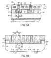
- FIGS. 5-8are top plan views of the substrate of FIG. 4 at subsequent stages in the fabrication of a self-assembled block copolymer film according to an embodiment of the disclosure.
- FIGS. 5A-8Aillustrate elevational, cross-sectional views of a portion of the substrate depicted in FIGS. 5-8 taken along lines 5 A- 5 A to 8 A- 8 A, respectively.
- FIGS. 5B-8Bare cross-sectional views of the substrate depicted in FIGS. 5-8 taken along lines 5 B- 5 B to 8 B- 8 B, respectively.
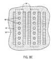
- FIG. 8Cis a top plan view of the substrate depicted in FIG. 8A taken along lines 8 C- 8 C.
- FIGS. 9-10are top plan views of the substrate of FIG. 8 at subsequent stages, illustrating an embodiment of the removal of one of the polymer blocks to form a mask to etch the substrate.
- FIGS. 9A-10Aillustrate elevational, cross-sectional views of a portion of the substrate depicted in FIGS. 9-10 taken along lines 9 A- 9 A and 10 A- 10 A, respectively.
- FIGS. 9B-10Bare cross-sectional views of the substrate depicted in FIGS. 9-10 taken along lines 9 B- 9 B to 10 B- 10 B, respectively.
- FIG. 11is a top plan view of the substrate of FIG. 10 at a subsequent stage, illustrating filling of the etched openings in the substrate.
- FIGS. 11A-11Billustrate elevational, cross-sectional views of a portion of the substrate depicted in FIG. 11 taken along lines 11 A- 11 A and 11 B- 11 B, respectively.
- semiconductor substrateor “semiconductive substrate” or “semiconductive wafer fragment” or “wafer fragment” or “wafer” will be understood to mean any construction comprising semiconductor material, including but not limited to bulk semiconductive materials such as a semiconductor wafer (either alone or in assemblies comprising other materials thereon), and semiconductive material layers (either alone or in assemblies comprising other materials).
- substraterefers to any supporting structure including, but not limited to, the semiconductive substrates, wafer fragments or wafers described above.
- L ois the inherent periodicity or pitch value (bulk period or repeat unit) of structures that self assemble upon annealing from a self-assembling (SA) block copolymer.
- L Bis the periodicity or pitch value of a blend of a block copolymer with one or more of its constituent homopolymers.
- Lis used herein to indicate the center-to-center cylinder pitch or spacing of cylinders of the block copolymer or blend, and is equivalent to “L o ” for a pure block copolymer and “L B ” for a copolymer blend.
- FIGS. 1-2illustrate the fabrication of a self-assembled film from a cylindrical-phase block copolymer (e.g., PS-b-P2VP) to form cylinders that are oriented parallel to the substrate surface.
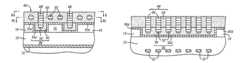
- a substrate 10(with active areas 12 ) is provided with an overlying material layer 14 that has been etched to form trenches 16 separated by spacers 18 .
- the trenchesinclude sidewalls 20 , ends 22 and a floor 24 that are preferential wetting to the minority block of the block copolymer material, e.g., oxide, etc.
- the width (w t ) of the trenches 16is about 1.5*L and the depth (D t ) is about L.
- the thickness (t) of the block copolymer material 26is about 0.5*L.
- annealingproduces a self-assembled film 28 composed of parallel cylinders 30 (diameter (d) ⁇ 0.5*L) of the minority block (e.g., P2VP) embedded within (or surrounded by) a matrix 32 of the majority block (e.g., PS) of the block copolymer material.
- a brush layer 30 a(thickness 0.5*L) forms on the preferential wetting surfaces (e.g., oxide, etc.) of the trenches and over the surface of the material layer 14 as a bilayer composed of the minority block wetting the trench surfaces.
- a layer of P2VP domainswill wet oxide interfaces, with attached PS domains directed away from the oxide material.
- the resulting film 28 with parallel cylinders 30can be used, for example, for patterning lines, but is not useful for fabricating an etch mask for patterning vias.
- a thickness of the block copolymer material 26 at about 1.5*Lis required at the time of annealing to produce the parallel cylinders as continuous lines.
- a polymer materiale.g., film, layer
- a polymer materialis prepared by guided self-assembly of block copolymers, with both polymer domains at the air interface.
- Block copolymer materialsspontaneously assemble into periodic structures by microphase separation of the constituent polymer blocks after annealing, forming ordered domains at nanometer-scale dimensions.
- a cylindrical-phase block copolymer layer with ordered structuresis formed as a base layer or film within a trench and used as a template to induce ordering of a subsequently deposited cylindrical-phase block copolymer resulting in a stacked double- or multi-layer structure having perpendicular-oriented cylinders in a polymer matrix.
- the pattern of perpendicular-oriented cylinders that is formedcan then be used, for example, as an etch mask for patterning nanosized features (e.g., vias) into the underlying substrate through selective removal of one block of the self-assembled block copolymer.
- nanosized featurese.g., vias
- FIGS. 3-8A method for fabricating a self-assembled block copolymer material that defines an array of nanometer-scale, perpendicular-oriented cylinders according to an embodiment of the invention is illustrated in FIGS. 3-8 .
- the described embodimentinvolves a thermal anneal of a cylindrical-phase block copolymer in combination with a graphoepitaxy technique that utilizes a lithographically defined trench as a guide with a floor, sidewalls and ends that are preferential wetting to one polymer block and function as constraints to induce self-assembly of the block copolymer of the base layer into an ordered one-dimensional (1-D) array of perpendicular-oriented cylindrical domains (“perpendicular cylinders”) within a polymer matrix, and the cylindrical-phase block copolymer of the overlying layer into cylinders in a polymer matrix oriented perpendicular and registered to the underlying perpendicular cylinders.
- multiple lines of the underlying perpendicular cylinderscan be formed in each trench with the overlying perpendicular-oriented cylinders.
- perpendicular cylindersused herein is understood to refer to the structure of the minority block of the base layer within the trenches, which shape can range from a half-sphere to an elongated cylinder with a rounded end, and is embedded within (surrounded by) a matrix of the majority block with a face wetting the air interface.
- the conditions provided in embodiments of the inventioninduce an orientational transition relative to the trench floor/substrate from parallel-oriented cylinders (“surface-parallel” cylinders) to perpendicular-oriented cylinders (“surface-normal” cylinders).
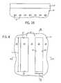
- a substrate 10 ′is provided.
- conductive lines 12 ′(or other active area, e.g., semiconducting regions) are situated within the substrate 10 ′.
- a material layer 14 ′(or one or more material layers) is formed over the substrate 10 ′ and etched to form trenches 16 ′ that are oriented perpendicular to an array of conductive lines 12 ′, as shown in FIGS. 4-4B . Portions of the material layer 14 ′ form a spacer 18 ′ outside and between the trenches.
- the trenches 16 ′are structured with opposing sidewalls 20 ′, opposing ends 22 ′, a floor 24 ′, a width (w t ), a length (l t ) and a depth (D t ).
- a single trench or multiple trenchescan be formed in the material layer 14 ′, and can span the entire width of an array of lines (or other active area).
- the substrate 10 ′is provided with an array of conductive lines 12 ′ (or other active areas) at a pitch of L.
- the trench or trenchesare formed over the active areas 12 ′ (e.g., lines) such that when the block copolymer material is annealed, each cylinder will be situated above a single active area 12 ′ (e.g., conductive line).
- multiple trenchesare formed with the ends 22 ′ of each adjacent trench 16 ′ aligned or slightly offset from each other at less than 5% of L such that cylinders in adjacent trenches are aligned and situated above the same line 12 ′.
- Single or multiple trenches 16 ′can be formed using a lithographic tool having an exposure system capable of patterning at the scale of L (10-100 nm).
- exposure systemsinclude, for example, extreme ultraviolet (EUV) lithography, proximity X-rays and electron beam (e-beam) lithography, as known and used in the art.
- EUVextreme ultraviolet
- e-beamelectron beam
- Conventional photolithographycan attain (at smallest) about 58 nm features.
- a method called “pitch doubling” or “pitch multiplication”can also be used for extending the capabilities of photolithographic techniques beyond their minimum pitch, as described, for example, in U.S. Pat. No. 5,328,810 (Lowrey et al.), U.S. Pat. No. 7,115,525 (Abatchev, et al.), US 2006/0281266 (Wells) and US 2007/0023805 (Wells).
- a pattern of linesis photolithographically formed in a photoresist material overlying a layer of an expendable material, which in turn overlies a substrate, the expendable material layer is etched to form placeholders or mandrels, the photoresist is stripped, spacers are formed on the sides of the mandrels, and the mandrels are then removed leaving behind the spacers as a mask for patterning the substrate.
- the initial photolithographyformed a pattern defining one feature and one space
- the same widthnow defines two features and two spaces, with the spaces defined by the spacers.
- the smallest feature size possible with a photolithographic techniqueis effectively decreased down to about 30 nm or less.
- Factors in forming a 1-D array of perpendicular cylinders within the trenchesinclude the width (w t ) of the trench, the formulation of the block copolymer or blend to achieve the desired pitch (L), and the total volume or thickness (t 2 ) of the block copolymer material within the trench at the end of the anneal at less than 2*L.
- the width (w t ) of the trenchcan be varied according to the desired number of rows and pattern of perpendicular cylinders.
- the trenches 16 ′are constructed with a width (w t ) of about 1.5*L (or 1.5 ⁇ the pitch value) of the block copolymer to form a single row of perpendicular cylinders.
- a cast block copolymer material (or blend) of about L and having a total thickness of less than 2*L at the end of annealwill self assemble within the trenches 16 ′ into perpendicular cylinders in a single row or line that is aligned with the sidewalls down the center of each trench 16 ′ with a center-to-center pitch distance (p) between adjacent perpendicular cylinders at or about the pitch distance or L value of the block copolymer material.
- the width (w t ) of the trenches 16 ′can be about 0.5*35 nm or about 55 nm to form a single row of perpendicular cylinders (each at about 20 nm diameter).
- a cylindrical-phase block copolymer with a pitch of L and having a total thickness of less than 2*L at the end of annealwill self-assemble to form perpendicular cylinders in a hexagonal array or a zigzag pattern with adjacent cylinders offset by about 0.5*L for the length (l t ) of the trench, rather than a single line row of perpendicular cylinders each separated by about L (center-to-center distance) and aligned with the sidewalls down the center of the trench.
- a cylindrical-phase block copolymer material having a L value of about 35 nm within a trench having a width of about 2-2.5*L or about 70-87.5 nmwill self assemble to form a hexagonal array of perpendicular cylinders (about 20 nm diameter) with a center-to-center pitch distance between adjacent cylinders of about 0.5*L value.
- the depth (D t ) of the trenches 16 ′is effective to direct lateral ordering of the block copolymer material during the anneal.
- the depth (D t ) of the trenches 16 ′is at or less than the final thickness (t 2 ) of the block copolymer material (D t ⁇ t 2 ), which minimizes the formation of a meniscus and variability in the thickness of the block copolymer material across the trench width.
- the trench depthis about 50-90% less, or about one-half to about two-thirds (about 1 ⁇ 2-2 ⁇ 3, or about 50%-67%) less than the final thickness (t 2 ) of the block copolymer material within the trench.
- the length (l t ) of the trenches 16 ′is according to the desired number of perpendicular cylinders in a row, and is generally at or about n*L or an integer multiple of L, and typically within a range of about n*10 to about n*100 nm (with n being the number of features or structures, e.g., perpendicular cylinders).
- the width of the mesas or spacers 18 ′ between adjacent trenchescan vary and is generally about L to about n*L.
- the trench dimensionis about 20-100 nm wide (w t ) and about 100-25,000 ⁇ m in length (l t ) with a depth (D t ) of about 10-100 nm.
- the trench sidewalls 20 ′, ends 22 ′ and floor 24 ′are preferential wetting by a minority block of the block copolymer to induce registration of cylinders (of the minority block) in a perpendicular orientation to the trench floor as the polymer blocks self-assemble to form the base layer 28 ′.
- the substrate 10 ′ and material layer 14 ′can be formed from the same or a highly similar material that is inherently preferential wetting to the minority (preferred) polymer block (e.g., PMMA of a PS-b-PMMA material) or, in other embodiments, a preferential wetting material can be applied onto the surfaces of the trenches 16 ′.
- the substrate 10 ′ and the material layer 14 ′can be composed of an inherently preferential wetting material such as a clean silicon surface (with native oxide), oxide (e.g., silicon oxide, SiO x ), silicon nitride, silicon oxycarbide, indium tin oxide (ITO), silicon oxynitride, and resist materials such as methacrylate-based resists and polydimethyl glutarimide resists, among other materials, which exhibit preferential wetting toward the preferred block (e.g., the minority block) (e.g., PMMA, PVP, etc.).
- a clean silicon surfacewith native oxide
- oxidee.g., silicon oxide, SiO x
- silicon nitridesilicon oxycarbide
- ITOindium tin oxide
- resist materialssuch as methacrylate-based resists and polydimethyl glutarimide resists, among other materials, which exhibit preferential wetting toward the preferred block (e.g., the minority block) (e.g.,
- the preferred (minority) blocke.g., the PMMA block, PVP block, etc.
- the preferred (minority) blockwill form a thin interface layer along the preferential wetting surfaces 20 ′, 22 ′, 24 ′ of the trenches.
- a preferential wetting materialsuch as a polymethylmethacrylate (PMMA) polymer modified with an —OH containing moiety (e.g., hydroxyethyl methacrylate) can be applied onto the surfaces of the trenches.
- PMMApolymethylmethacrylate
- An OH-modified PMMAcan be applied, for example, by spin coating and then heating (e.g., to about 170° C.) to allow the terminal —OH groups to end-graft to oxide surfaces (e.g., sidewalls 20 ′, ends 22 ′, floor 24 ′).
- Non-grafted materialcan be removed by rinsing with an appropriate solvent (e.g., toluene). See, for example, Mansky et al., Science, 1997, 275, 1458-1460, and In et al., Langmuir, 2006, 22, 7855-7860.
- a self-assembling, cylindrical-phase block copolymer material 26 ′ having an inherent pitch at or about L o (or a ternary blend of block copolymer and homopolymers blended to have a pitch at or about L B )is deposited into the trenches 16 ′ to form a base layer 28 ′.
- Nonlimiting examples of diblock copolymersinclude, for example, poly(styrene)-b-poly(methylmethacrylate) (PS-b-PMMA) or other PS-b-poly(acrylate) or PS-b-poly(methacrylate), poly(styrene)-b-poly(vinylpyridine) (PS-b-PVP), poly(styrene)-b-poly(lactide) (PS-b-PLA), and poly(styrene)-b-poly(tert-butyl acrylate) (PS-b-PtBA), poly(styrene)-b-poly(ethylene-co-butylene (PS-b-(PS-co-PB)), poly(styrene)-b-poly(ethylene oxide) (PS-b-PEO), polybutadiene-b-poly(vinylpyridine) (PB-b-PVP), poly(ethylene-alt-propylene)-b-pol
- block copolymersi.e., triblock or multiblock copolymers
- triblock copolymersinclude ABC copolymers such as poly(styrene-b-methyl methacrylate-b-ethylene oxide) (PS-b-PMMA-b-PEO), and ABA copolymers such as PS-PMMA-PS, PMMA-PS-PMMA, and PS-b-PI-b-PS, among others.
- the block copolymer or blendis constructed such that the minor domain can be selectively removed.
- the L value of the block copolymercan be modified, for example, by adjusting the molecular weight of the block copolymer.
- the block copolymer materialcan also be formulated as a binary or ternary blend comprising a block copolymer and one or more homopolymers (HPs) of the same type of polymers as the polymer blocks in the block copolymer, to produce a blend that will swell the size of the polymer domains and increase the L value.
- the concentration of homopolymers in a blendcan range from 0 to about 60 wt-%. Generally, when added to a polymer material, both homopolymers are added to the blend in about the same ratio or amount.
- a ternary diblock copolymer/homopolymer blendis a PS-b-PVP/PS/PVP blend, for example, 60 wt-% of 32.5 K/12 K PS-b-PVP, 20 wt-% of 10K PS, and 20 wt-% of 10K PVP.
- Another example of a ternary diblock copolymer/homopolymer blendis a PS-b-PMMA/PS/PMMA blend, for example, 60 wt-% of 46K/21K PS-b-PMMA, 20 wt-% of 20K polystyrene and 20 wt-% of 20K poly(methyl methacrylate).
- Yet another exampleis a blend of 60:20:20 (wt-%) of PS-b-PEO/PS/PEO, or a blend of about 85-90 wt-% PS-b-PEO and up to 10-15 wt-% PEO homopolymer.
- the film morphologyincluding the domain sizes and periods (L) of the microphase-separated domains, can be controlled by chain length of a block copolymer (molecular weight, MW) and volume fraction of the AB blocks of a diblock copolymer to produce cylindrical morphologies (among others).
- a block copolymermolecular weight, MW
- volume fraction of the AB blocks of a diblock copolymerto produce cylindrical morphologies (among others).
- the diblock copolymerwill microphase separate and self-assemble into periodic perpendicular cylinder domains of polymer B within a matrix of polymer A.
- An example of a cylinder-forming PS-b-PVP copolymer material (L o ⁇ 28 nm) to form about 14 nm diameter perpendicular cylinder PVP domains in a matrix of PSis composed of about 70 wt-% PS and 30 wt-% PVP with a total molecular weight (M n ) of 44.5 kg/mol.
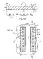
- the block copolymer materialcan be deposited by spin casting (spin-coating) from a dilute solution (e.g., about 0.25-2 wt % solution) of the block copolymer in an organic solvent such as dichloroethane (CH 2 Cl 2 ) or toluene, for example. Capillary forces pull excess block copolymer material 26 ′ (e.g., greater than a monolayer) into the trenches 16 ′. As shown in FIG. 5A , a thin layer or film 26 a ′ of the block copolymer material can be deposited onto the material layer 14 ′ outside the trenches, e.g., on the mesas/spacers 18 ′.
- the thin film 26 a ′(in excess of a monolayer) will flow off the mesas/spacers 18 ′ into the trenches leaving a structureless brush layer on the material layer 14 ′ from a top-down perspective.
- the block copolymer material 26 ′is then annealed to form the self-assembled base layer 28 ′.
- the cylindrical-phase block copolymer materiale.g., PS-b-PMMA
- the cylindrical-phase block copolymer materialwill self-assemble in response to the constraints provided by the width (w t ) of the trench 16 ′ and the character of the cylindrical-phase block copolymer composition 26 ′ (e.g., PS-b-PMMA having an inherent pitch at or about L) combined with trench surfaces 20 ′, 22 ′, 24 ′ that are preferential wetting by the minority or preferred block of the block copolymer (e.g., the PMMA block), and a total thickness (t 2 ) of the BCP material 26 ′ within the trench of less than 2*L at the end of anneal.
- the minority or preferred block of the block copolymere.g., the PMMA block
- the width (w) of the trenchis greater than 1.5*L
- an ordered hexagonal array of perpendicular cylinderscan be formed in each trench.
- the resulting base layer 28 ′is composed of a monolayer of perpendicular cylinder domains 34 ′ of the preferred (minority) block (e.g., PMMA) within a matrix 36 ′ of the majority polymer block (e.g., PS) oriented perpendicular to the trench floor 24 ′ and registered and aligned parallel to the trench sidewalls 20 ′ in a row down the middle of each trench for the length of the trench and spaced apart at a center-to-center pitch distance of about L.
- the face 38 ′ of the perpendicular cylinderswets the air interface (surface exposed) and the opposing ends 40 ′ are embedded in (surrounded by) the polymer matrix 36 ′.
- the diameter (d) of the perpendicular cylinders 34 ′will generally be about one-half of the center-to-center distance (pitch distance, p) between the perpendicular cylinders.
- a layer of the minority (preferred) blocksegregates to and wets the sidewalls 20 ′, ends 22 ′ and floor 24 ′ of the trenches to form a thin brush wetting layer 34 a ′ with a thickness of generally about 0.5*L.
- the brush layer 34 a ′is a bilayer of the minority block domains (e.g., PMMA) wetting trench (e.g., oxide) interfaces with attached majority block domains (e.g., PS) directed away from the trench surfaces and in contact with the majority block domains (e.g., PS) of the matrix 36 ′ at the surface of the perpendicular cylinder domains 34 ′.
- the minority block domainse.g., PMMA
- trenche.g., oxide
- majority block domainse.g., PS
- the resulting morphology of the annealed polymer material base layer 28 ′i.e., the perpendicular orientation of the perpendicular cylinders 34 ′, can be examined, for example, using atomic force microscopy (AFM), transmission electron microscopy (TEM), scanning electron microscopy (SEM).
- AFMatomic force microscopy
- TEMtransmission electron microscopy
- SEMscanning electron microscopy
- the self-assembled base layer 28 ′is defined by an array of perpendicular cylinders 34 ′ in a polymer matrix 36 ′ and a brush layer 34 a ′ (at about 0.5*L thick), each cylinder 34 ′ having a rounded end 40 ′ and a diameter at or about 0.5*L, with the number (n) of perpendicular cylinders in the row according to the length of the trench, and the center-to-center distance (pitch distance, p) between perpendicular cylinders at or about L.
- the block copolymer material 26 ′is cast into the trenches 16 ′ to an initial thickness (t 1 ) such that upon completion of inflow of polymer material off the mesas/spacers 18 ′ into the trenches and at the end of the anneal, the total volume or thickness (t 2 ) of the block copolymer material 26 ′ will induce and result in the formation of perpendicular cylinders 34 ′ in the trench.
- the block copolymer material 26 ′ within the trenches at the end of the annealhas an insufficient volume of polymer material to fully form surface parallel cylinders ( 30 ) that would typically result under the same or similar conditions (e.g., of trench width (w t ), trench depth (D t ), block copolymer material at about L, preferentially wetting trench surfaces).
- the total volume or thickness (t 2 ) of the block copolymer (BCP) material 26 ′ after the annealis effective to induce a transition from a surface parallel to a surface normal (or perpendicular) orientation of cylindrical domains relative to the trench floor/substrate surface.
- the thickness of the block copolymer material 26 ′can be measured, for example, by ellipsometry techniques.
- the face 38 ′ of the perpendicular cylinders 34 ′wets the air interface and the opposing ends 40 ′ are rounded.
- the total volume or thickness (t 2 ) of a PS-b-P2VP block copolymer material 26 ′ (or similar polymer material) after inflow from the mesas/spacers 18 ′ and at the end of annealis about 5-30% less (or about 10-20% less) than the 1.5*L value of the block copolymer material, or t 2 ⁇ 70-95%*(1.5*L).
- the PS-b-P2VP block copolymer material 26 ′can be cast into the trenches 16 ′ and the polymer material 26 a ′ caused to flow into the trenches wherein the total volume or thickness (t 2 ) of the block copolymer material 26 ′ at the end of anneal is [(about 0.70 to about 0.95)*(1.5*35 nm)], or about 36.75-49.9 nm thick.
- the typical thickness (t 2 ) of the block copolymer material 26 to form a monolayer of parallel cylinders (over a brush layer 30 a ) ( FIGS. 1-2 )is generally t 2 ⁇ L.
- a film 26 ′ of a block copolymer material such as PS-b-PMMA within the trenches 16 ′ at the end of annealshould be at less than the L value or t 2 ⁇ L to result in a reorientation of the cylinders from parallel to perpendicular with a brush layer 34 a ′ in contact with the trench surfaces 20 ′, 22 ′, 24 ′.
- the cylinders 34 ′have a shorter length and appear as half-spheres due to the rounded ends 40 ′.
- the total volume or thickness (t 2 ) of a PS-b-PMMA block copolymer material 26 ′ (or similar material) after inflow from the mesas/spacers 18 ′ and at the end of annealis about 5-30% less (or about 10-20% less) than the L value of the block copolymer material, or t 2 ⁇ 70-95%*(1*L).
- the PS-b-PMMA block copolymer material 26 ′can be cast into the trenches 16 ′ and the polymer material 26 a ′ caused to flow into the trenches wherein the total volume or thickness (t 2 ) of the block copolymer material 26 ′ after the anneal is [(about 0.70 to about 0.95)*(35 nm)], or about 24.5-33.25 nm thick, resulting in surface normal (perpendicular) cylinders 34 ′ within the trenches.
- a film 26 ′ of a block copolymer material such as PS-b-PDMS within trenches 16 ′ at the end of annealshould have a thickness (t 2 ) of less than about 2*L (or at t 2 ⁇ 2*L) to result in a reorientation to perpendicular cylinders 34 ′ ( FIG. 6A ) in which the cylinders are perpendicular to the trench floor 24 ′ with rounded ends 40 ′.
- the total volume or thickness (t 2 ) of PS-b-PDMS block copolymer material 26 ′ (or similar material) after annealis about 5-30% less (or about 10-20% less) than 2*L value of the block copolymer material, or t 2 ⁇ 70-95%*(2*L).
- the PS-b-PDMS block copolymer material 26 ′can be cast into the trenches 16 ′ and the polymer material 26 a ′ caused to flow into the trenches wherein the total volume or thickness (t 2 ) of the block copolymer material 26 ′ after the anneal is [(about 0.70 to about 0.95)*(2*35 nm)], or about 49-66.5 nm thick.
- the polymer material 26 ′can be annealed to form the polymer base layer 28 ′, for example, by thermal annealing to above the glass transition temperature of the component blocks of the copolymer material to cause the polymer blocks to separate and self assemble in response to the preferential wetting of the trench surfaces 20 ′, 22 ′, 24 ′.
- a PS-b-PMMA copolymer filmcan be annealed at a temperature of about 150-275° C. in a vacuum oven for about 1-24 hours to achieve the self-assembled morphology.
- the block copolymer material 26 ′can be globally heated or, in other embodiments, a zone or localized thermal anneal can be applied to portions or sections of the block copolymer material 26 ′.
- the substratecan be moved across a temperature gradient 42 ′ ( FIG. 6A ), for example, a hot-to-cold temperature gradient, positioned above (as shown) or underneath the substrate (or the thermal source can be moved relative to the substrate, e.g., arrow ⁇ ) such that the block copolymer material self-assembles upon cooling after passing through the heat source.
- the base layer (film) 28 ′can then be treated to crosslink one of the polymer domains to fix and enhance the strength of the polymer domain, for example, the polymer matrix 36 ′ (e.g., the PS segments to make the PS matrix insoluble).
- the polymer blockcan be structured to inherently crosslink (e.g., upon UV exposure) or formulated to contain a crosslinking agent.
- the block copolymer material 26 a ′ outside the trencheswill not be thick enough to result in self-assembly.
- the unstructured thin film 26 a ′ of the block copolymer material outside the trenchescan be removed, as illustrated in FIGS. 6A-6B , for example, by an etch technique or a planarization process.
- the trench regionscan be selectively exposed through a reticle (not shown) to crosslink only the annealed and self-assembled polymer material 28 ′ within the trenches 16 ′, and a wash can then be applied with an appropriate solvent (e.g., toluene) to remove the non-crosslinked portions of the block copolymer material 26 a ′ (e.g., on the spacers 18 ′), leaving the registered self-assembled base layer 28 ′ within the trench and exposing the surface ( 18 ′) of the material layer 14 ′ above/outside the trenches.
- an appropriate solvente.g., toluene
- the polymer material 26 ′can be crosslinked globally, a photoresist material can be applied to pattern and expose the areas of the polymer material 26 a ′ outside the trench regions, and the exposed portions of the polymer material 26 a ′ can be removed, for example by an oxygen (O 2 ) plasma treatment.
- O 2oxygen
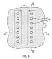
- the annealed and self-assembled base film 28 ′is then used as a template for inducing the ordering of an overlying cylindrical-phase block copolymer material such that the cylindrical domains of the annealed second film will orient perpendicular and registered to the underlying pattern of perpendicular cylinders in the base film.
- a cylindrical-phase block copolymer (BCP) material 44 ′ having an inherent pitch at or about the L value of the block copolymer material 26 ′ of the base layer 28 ′ (or a ternary blend of block copolymer and homopolymers blended to have a pitch at or about the L value)is deposited (e.g., by spin casting) onto the annealed (and crosslinked) base layer 28 ′ within the trenches 16 ′.
- the block copolymer material 44 ′can be deposited to a thickness (t 3 ) at or about its L value.
- the minority domain of the BCP material 44 ′is either identical to or preferentially wets the perpendicular cylinder (minority) domains 34 ′ of the underlying base layer 28 ′.
- the block copolymer material 44 ′is then annealed to form a self-assembled material layer 46 ′ over the base layer 28 ′, as depicted in FIGS. 8A-8C .
- the polymer material 44 ′can be annealed, for example, by thermal annealing.
- the chemical pattern of the perpendicular cylinder (minor) domains 34 ′ of the base layer 28 ′templates and imposes an induced ordering effect on the self-assembling cylindrical-phase block copolymer material 44 ′ to form a layer 46 ′ of perpendicular-oriented cylinders 48 ′ of the minority (preferred) block (e.g., PMMA) within a polymer matrix 50 ′ of the majority block (e.g., PS), with the cylinders registered to the underlying pattern of perpendicular cylinders 34 ′ of the base layer 28 ′.
- the diameter of the perpendicular cylinders 48 ′is at or about 0.5*L.
- parallel cylinders 30 ′ embedded in the matrix 50 a ′ and a brush layer 30 a ′will form over the preferential wetting material layer 14 ′, as shown in FIGS. 8A-8B .
- Intrinsic periods of the two block copolymer materials 26 ′, 44 ′can be matched, for example, through a ternary blend of either or both of the copolymer materials with one or more homopolymers to adjust the polymer periods (L values). See, for example, R. Ruiz, R. L. Sandstrom and C. T. Black, “Induced Orientational Order in Symmetric Diblock Copolymer Thin-Films,” Advanced Materials, 2007, 19(4), 587-59.
- the same cylindrical-phase block copolymer materialis used for both block copolymer materials 26 ′, 44 ′.
- the annealed and self-assembled polymer layer 46 ′can then be treated to cross-link one of the polymer segments (e.g., the PS matrix 50 ′), as previously described.
- one of the block componentscan be selectively removed to produce a porous film that can be used, for example, as a lithographic template or mask to pattern the underlying substrate 10 ′ in a semiconductor processing to define a regular pattern of nanometer sized openings (i.e., about 10-100 nm).
- the cylindrical domains 48 ′ and the underlying perpendicular cylinders 34 ′ of the base layer 28 ′are selectively removed to form a porous film of regular cylindrical-shaped voids or openings 54 ′ within a polymer matrix 36 ′, 50 ′ that are registered to the trench sidewalls 20 ′.
- selective removal of PMMA domains 34 ′, 48 ′ from a cross-linked PS matrix 36 ′, 50 ′can be performed, for example, by application of an oxygen (O 2 ) plasma, or by a chemical dissolution process such as acetic acid sonication by first irradiating the sample (ultraviolet (UV) radiation, 1 J/cm ⁇ 2 254 nm light), then ultrasonicating the film in glacial acetic acid, ultrasonicating in deionized water, and rinsing the film in deionized water to remove the degraded PMMA.
- O 2oxygen
- acetic acid sonicationby first irradiating the sample (ultraviolet (UV) radiation, 1 J/cm ⁇ 2 254 nm light), then ultrasonicating the film in glacial acetic acid, ultrasonicating in deionized water, and rinsing the film in deionized water to remove the degraded PMMA.
- a portion of the PS matrix 36 ′ situated underneath the openings 54 ′ and over the trench floor 24 ′remains after the removal of the PMMA domains 34 ′, 48 ′.
- the underlying PS matrix 36 ′can be removed, for example, by a reactive ion etch (RIE) using an oxygen plasma, for example, to expose the underlying substrate 10 ′ at the trench floor 24 ′, as illustrated in FIGS. 10-10B .
- the resulting polymer film 52 ′is composed of cylindrical openings 54 ′ within the polymer matrix 36 ′, 50 ′ (e.g., of PS).
- the RIE etchmay thin the polymer matrix 50 ′, as shown, although not to a significant extent.
- An embodiment of the application of the polymer film 52 ′is as an etch mask to form openings in the substrate 10 ′.
- the polymer film 52 ′can then be used as a mask to etch (arrows ⁇ ) a series of cylindrical openings or contact holes 56 ′ (shown in phantom) to the conductive lines 12 ′ or other active area (e.g., semiconducting region, etc.) in the underlying substrate 10 ′ (or an underlayer), for example, using a selective RIE plasma etch process.
- the residual polymer material 52 ′(e.g., 50 ′, 34 a ′, 36 ′) can be removed and the substrate openings 56 ′ can be filled with a material 58 ′ such as a metal or metal alloy such as Cu, Al, W, Si, and Ti 3 N 4 , among others, to form arrays of cylindrical contacts to the conductive lines 12 ′.
- the cylindrical openings 56 ′ in the substratecan also be filled with a metal-insulator-metal stack to form capacitors with an insulating material such as SiO 2 , Al 2 O 3 , HfO 2 , ZrO 2 , SrTiO 3 , and the like.
- Methods of the disclosureprovide a means of generating self-assembled diblock copolymer films composed of perpendicular-oriented cylinders in a polymer matrix.
- the methodsprovide ordered and registered elements on a nanometer scale that can be prepared more inexpensively than by electron beam lithography, EUV photolithography or conventional photolithography.
- the feature sizes produced and accessible by this inventioncannot be easily prepared by conventional photolithography. Since the domain sizes and periods (L) involved in this method are determined by the chain length of a block copolymer (MW), resolution can exceed other techniques such as conventional photolithography. Processing costs using the technique are significantly less than extreme ultraviolet (EUV) photolithography, which has comparable resolution.
- EUVextreme ultraviolet
- Embodiments of the inventioneliminate the need for preparing trench floors that wet both blocks of a block copolymer to form perpendicular-oriented cylinders from block copolymer materials. While forming a neutral wetting trench floor can be accomplished, for example, by forming a neutral wetting material (e.g., random copolymer material) on the trench floor, it requires either processes that are not conventional to semiconductor manufacturing and/or extra processing steps. The present methods do not require unconventional processes for manufacturing the required structures.
- a neutral wetting materiale.g., random copolymer material
- embodiments of the disclosure providing chemical pattern templating of the upper layerprovide fast processing of BCP materials relative to other methods of registering block copolymers such as processes that utilize graphoepitaxy with selective/neutral wetting trench or groove surfaces alone.
- the present methodsprovide formation of nanostructures in a manner that is more readily manufacturable.
Landscapes
- Physics & Mathematics (AREA)
- General Physics & Mathematics (AREA)
- Exposure Of Semiconductors, Excluding Electron Or Ion Beam Exposure (AREA)
Abstract
Description
Claims (35)
Priority Applications (2)
| Application Number | Priority Date | Filing Date | Title |
|---|---|---|---|
| US12/106,562US8114300B2 (en) | 2008-04-21 | 2008-04-21 | Multi-layer method for formation of registered arrays of cylindrical pores in polymer films |
| US13/396,261US8455082B2 (en) | 2008-04-21 | 2012-02-14 | Polymer materials for formation of registered arrays of cylindrical pores |
Applications Claiming Priority (1)
| Application Number | Priority Date | Filing Date | Title |
|---|---|---|---|
| US12/106,562US8114300B2 (en) | 2008-04-21 | 2008-04-21 | Multi-layer method for formation of registered arrays of cylindrical pores in polymer films |
Related Child Applications (1)
| Application Number | Title | Priority Date | Filing Date |
|---|---|---|---|
| US13/396,261DivisionUS8455082B2 (en) | 2008-04-21 | 2012-02-14 | Polymer materials for formation of registered arrays of cylindrical pores |
Publications (2)
| Publication Number | Publication Date |
|---|---|
| US20090263628A1 US20090263628A1 (en) | 2009-10-22 |
| US8114300B2true US8114300B2 (en) | 2012-02-14 |
Family
ID=41201358
Family Applications (2)
| Application Number | Title | Priority Date | Filing Date |
|---|---|---|---|
| US12/106,562ActiveUS8114300B2 (en) | 2008-04-21 | 2008-04-21 | Multi-layer method for formation of registered arrays of cylindrical pores in polymer films |
| US13/396,261ActiveUS8455082B2 (en) | 2008-04-21 | 2012-02-14 | Polymer materials for formation of registered arrays of cylindrical pores |
Family Applications After (1)
| Application Number | Title | Priority Date | Filing Date |
|---|---|---|---|
| US13/396,261ActiveUS8455082B2 (en) | 2008-04-21 | 2012-02-14 | Polymer materials for formation of registered arrays of cylindrical pores |
Country Status (1)
| Country | Link |
|---|---|
| US (2) | US8114300B2 (en) |
Cited By (24)
| Publication number | Priority date | Publication date | Assignee | Title |
|---|---|---|---|---|
| US20100155690A1 (en)* | 2008-12-18 | 2010-06-24 | Stmicroelectronics S.R.L. | Cross-point cell nanoarray with anisotropic active organic layer |
| US20120094087A1 (en)* | 2007-03-06 | 2012-04-19 | Millward Dan B | Registered Structure Formation via the Application of Directed Thermal Energy to Diblock Copolymer Films |
| US8445592B2 (en) | 2007-06-19 | 2013-05-21 | Micron Technology, Inc. | Crosslinkable graft polymer non-preferentially wetted by polystyrene and polyethylene oxide |
| US8450418B2 (en) | 2010-08-20 | 2013-05-28 | Micron Technology, Inc. | Methods of forming block copolymers, and block copolymer compositions |
| US8455082B2 (en) | 2008-04-21 | 2013-06-04 | Micron Technology, Inc. | Polymer materials for formation of registered arrays of cylindrical pores |
| US8518275B2 (en) | 2008-05-02 | 2013-08-27 | Micron Technology, Inc. | Graphoepitaxial self-assembly of arrays of downward facing half-cylinders |
| US8551808B2 (en) | 2007-06-21 | 2013-10-08 | Micron Technology, Inc. | Methods of patterning a substrate including multilayer antireflection coatings |
| US8557128B2 (en) | 2007-03-22 | 2013-10-15 | Micron Technology, Inc. | Sub-10 nm line features via rapid graphoepitaxial self-assembly of amphiphilic monolayers |
| US20130270621A1 (en)* | 2012-04-16 | 2013-10-17 | Kabushiki Kaisha Toshiba | Nonvolatile semiconductor storage device and fabrication method thereof |
| US8609221B2 (en) | 2007-06-12 | 2013-12-17 | Micron Technology, Inc. | Alternating self-assembling morphologies of diblock copolymers controlled by variations in surfaces |
| US8633112B2 (en) | 2008-03-21 | 2014-01-21 | Micron Technology, Inc. | Thermal anneal of block copolymer films with top interface constrained to wet both blocks with equal preference |
| US8642157B2 (en) | 2008-02-13 | 2014-02-04 | Micron Technology, Inc. | One-dimensional arrays of block copolymer cylinders and applications thereof |
| US8641914B2 (en) | 2008-03-21 | 2014-02-04 | Micron Technology, Inc. | Methods of improving long range order in self-assembly of block copolymer films with ionic liquids |
| US8669645B2 (en) | 2008-10-28 | 2014-03-11 | Micron Technology, Inc. | Semiconductor structures including polymer material permeated with metal oxide |
| US8900963B2 (en) | 2011-11-02 | 2014-12-02 | Micron Technology, Inc. | Methods of forming semiconductor device structures, and related structures |
| US8956713B2 (en) | 2007-04-18 | 2015-02-17 | Micron Technology, Inc. | Methods of forming a stamp and a stamp |
| US8980755B2 (en) | 2012-09-05 | 2015-03-17 | Kabushiki Kaisha Toshiba | Method of pattern formation |
| US8999492B2 (en) | 2008-02-05 | 2015-04-07 | Micron Technology, Inc. | Method to produce nanometer-sized features with directed assembly of block copolymers |
| US20150154997A1 (en)* | 2012-01-31 | 2015-06-04 | Seagate Technology Llc | Combining features using directed self-assembly to form patterns for etching |
| US9087699B2 (en) | 2012-10-05 | 2015-07-21 | Micron Technology, Inc. | Methods of forming an array of openings in a substrate, and related methods of forming a semiconductor device structure |
| US9142420B2 (en) | 2007-04-20 | 2015-09-22 | Micron Technology, Inc. | Extensions of self-assembled structures to increased dimensions via a “bootstrap” self-templating method |
| US9177795B2 (en) | 2013-09-27 | 2015-11-03 | Micron Technology, Inc. | Methods of forming nanostructures including metal oxides |
| US9229328B2 (en) | 2013-05-02 | 2016-01-05 | Micron Technology, Inc. | Methods of forming semiconductor device structures, and related semiconductor device structures |
| US9279191B2 (en) | 2012-09-07 | 2016-03-08 | Kabushiki Kaisha Toshiba | Pattern forming method |
Families Citing this family (16)
| Publication number | Priority date | Publication date | Assignee | Title |
|---|---|---|---|---|
| US8394483B2 (en) | 2007-01-24 | 2013-03-12 | Micron Technology, Inc. | Two-dimensional arrays of holes with sub-lithographic diameters formed by block copolymer self-assembly |
| KR101027677B1 (en)* | 2008-09-09 | 2011-04-12 | 주식회사 하이닉스반도체 | Contact hole formation method of semiconductor device |
| US8361704B2 (en)* | 2009-01-12 | 2013-01-29 | International Business Machines Corporation | Method for reducing tip-to-tip spacing between lines |
| KR101101767B1 (en)* | 2009-05-07 | 2012-01-05 | 한국과학기술원 | Coil-comb block copolymer and method for manufacturing nanostructure using same |
| US8563086B2 (en) | 2009-07-22 | 2013-10-22 | Korea Institute Research and Business Foundation | Nano pattern formation |
| US8592732B2 (en) | 2009-08-27 | 2013-11-26 | Korea University Research And Business Foundation | Resistive heating device for fabrication of nanostructures |
| JP5254381B2 (en)* | 2011-02-23 | 2013-08-07 | 株式会社東芝 | Pattern formation method |
| US9478429B2 (en)* | 2012-03-13 | 2016-10-25 | Massachusetts Institute Of Technology | Removable templates for directed self assembly |
| KR102003334B1 (en)* | 2012-09-04 | 2019-07-24 | 삼성전자주식회사 | Method of forming patterns |
| KR102394998B1 (en) | 2013-09-04 | 2022-05-04 | 도쿄엘렉트론가부시키가이샤 | Uv-assisted stripping of hardened photoresist to create chemical templates for directed self-assembly |
| US9793137B2 (en)* | 2013-10-20 | 2017-10-17 | Tokyo Electron Limited | Use of grapho-epitaxial directed self-assembly applications to precisely cut logic lines |
| US9653349B2 (en)* | 2014-01-24 | 2017-05-16 | Taiwan Semiconductor Manufacturing Company, Ltd. | Semiconductor integrated circuit with nano gap |
| US9385129B2 (en)* | 2014-11-13 | 2016-07-05 | Tokyo Electron Limited | Method of forming a memory capacitor structure using a self-assembly pattern |
| KR20160087479A (en)* | 2015-01-13 | 2016-07-22 | 에스케이하이닉스 주식회사 | Semiconductor device and manufacturing method thereof |
| US9947597B2 (en) | 2016-03-31 | 2018-04-17 | Tokyo Electron Limited | Defectivity metrology during DSA patterning |
| WO2019008602A1 (en)* | 2017-07-06 | 2019-01-10 | INDIAN INSTITUTE OF TECHNOLOGY MADRAS (IIT Madras) | Bi-layer resist approach of photolithographic patterning over pmma based polymer dielectrics |
Citations (140)
| Publication number | Priority date | Publication date | Assignee | Title |
|---|---|---|---|---|
| US4623674A (en) | 1985-06-21 | 1986-11-18 | Union Carbide Corporation | Polymer/polyols of substituted styrenes and polyurethanes made therefrom |
| US4877647A (en) | 1986-04-17 | 1989-10-31 | Kansas State University Research Foundation | Method of coating substrates with solvated clusters of metal particles |
| US5482656A (en) | 1993-03-04 | 1996-01-09 | Kabushiki Kaisha Toshiba | Non-linear optical devices employing a polysilane composition and a polysilane composition therefor |
| US5538655A (en) | 1994-06-29 | 1996-07-23 | Arthur D. Little, Inc. | Molecular complexes for use as electrolyte components |
| US5622668A (en) | 1992-02-07 | 1997-04-22 | The United States Of America As Represented By The Secretary Of The Air Force | Method for preparing oriented polymer structures and said structures |
| US5904824A (en) | 1997-03-07 | 1999-05-18 | Beckman Instruments, Inc. | Microfluidic electrophoresis device |
| US5948470A (en) | 1997-04-28 | 1999-09-07 | Harrison; Christopher | Method of nanoscale patterning and products made thereby |
| EP0784543B1 (en) | 1995-08-04 | 2000-04-26 | International Business Machines Corporation | Lithographic surface or thin layer modification |
| US6111323A (en) | 1997-12-30 | 2000-08-29 | International Business Machines Corporation | Reworkable thermoplastic encapsulant |
| US6143647A (en) | 1997-07-24 | 2000-11-07 | Intel Corporation | Silicon-rich block copolymers to achieve unbalanced vias |
| US6368871B1 (en) | 1997-08-13 | 2002-04-09 | Cepheid | Non-planar microstructures for manipulation of fluid samples |
| US6403382B1 (en) | 1998-12-08 | 2002-06-11 | Regents Of The University Of Minnesota | Attachment chemistry for organic molecules to silicon |
| US6423465B1 (en) | 2000-01-28 | 2002-07-23 | International Business Machines Corporation | Process for preparing a patterned continuous polymeric brush on a substrate surface |
| US6503841B1 (en) | 2000-07-07 | 2003-01-07 | Agere Systems Inc. | Oxide etch |
| US6506660B2 (en)* | 2000-11-15 | 2003-01-14 | International Business Machines Corporation | Semiconductor with nanoscale features |
| US6548830B1 (en) | 1996-05-22 | 2003-04-15 | Sony Corporation | Semiconductor device formed of single crystal grains in a grid pattern |
| US20030077452A1 (en) | 2001-07-17 | 2003-04-24 | Guire Patrick E. | Self assembling monolayer compositions |
| US20030091752A1 (en) | 2001-10-05 | 2003-05-15 | Nealey Paul F. | Guided self-assembly of block copolymer films on interferometrically nanopatterned substrates |
| US6566248B1 (en) | 2001-01-11 | 2003-05-20 | Advanced Micro Devices, Inc. | Graphoepitaxial conductor cores in integrated circuit interconnects |
| US6565763B1 (en) | 1999-06-07 | 2003-05-20 | Kabushiki Kaisha Toshiba | Method for manufacturing porous structure and method for forming pattern |
| US6569528B2 (en) | 2001-06-23 | 2003-05-27 | Pacific Corporation | Amphiphilic biodegradable block copolymers and self-assembled polymer aggregates formed from the same in aqueous milieu |
| US20030100822A1 (en) | 2001-09-01 | 2003-05-29 | Seok Lew | Analyte measuring biosensor chip using image scanning system |
| US20030185741A1 (en) | 2001-04-06 | 2003-10-02 | Krzysztof Matyjaszewski | Process for the preparation of nanostructured materials |
| US6699797B1 (en) | 2002-12-17 | 2004-03-02 | Intel Corporation | Method of fabrication of low dielectric constant porous metal silicate films |
| US6713238B1 (en) | 1998-10-09 | 2004-03-30 | Stephen Y. Chou | Microscale patterning and articles formed thereby |
| US20040084298A1 (en) | 2002-10-31 | 2004-05-06 | Y.D. Yao | Fabrication of nanocomposite thin films for high density magnetic recording media |
| EP1416303A2 (en) | 2002-10-30 | 2004-05-06 | Hitachi, Ltd. | Functioning substrate with a group of columnar micro pillars and its manufacturing method |
| US20040124092A1 (en) | 2002-12-30 | 2004-07-01 | Black Charles T. | Inorganic nanoporous membranes and methods to form same |
| US20040127001A1 (en) | 2002-12-27 | 2004-07-01 | International Business Machines Corporation | Robust ultra-low k interconnect structures using bridge-then-metallization fabrication sequence |
| US20040142578A1 (en) | 2002-03-28 | 2004-07-22 | Ulrich Wiesner | Thin film nanostructures |
| US6781166B2 (en) | 1999-07-02 | 2004-08-24 | President & Fellows Of Harvard College | Nanoscopic wire-based devices and arrays |
| US20040192013A1 (en) | 2003-03-31 | 2004-09-30 | Ryu Myung Kwan | Method for fabricating single crystal silicon film |
| US20040222415A1 (en) | 2003-03-11 | 2004-11-11 | Industrial Technology Research Institute | Organic device including semiconducting layer aligned according to microgrooves of photoresist layer |
| US20040254317A1 (en) | 2003-06-12 | 2004-12-16 | Jinlian Hu | Methods for producing di-block polymers |
| US20040256615A1 (en) | 2001-07-09 | 2004-12-23 | Henning Sirringhaus | Lamellar polymer architecture |
| US20040256662A1 (en) | 2003-06-20 | 2004-12-23 | International Business Machines Corporation | Nonvolatile memory device using semiconductor nanocrystals and method of forming same |
| US20040265548A1 (en) | 2003-05-20 | 2004-12-30 | Rong-Ming Ho | Nanopatterned templates from oriented degradable diblock copolymer thin films |
| CN1562730A (en) | 2004-03-24 | 2005-01-12 | 哈尔滨工业大学 | Method for adjusting and controlling configuration of self-assembling block copolymer template oriented to nano micro machining |
| JP2005008882A (en) | 1999-06-07 | 2005-01-13 | Toshiba Corp | Porous structure manufacturing method, porous structure forming material, pattern forming method, pattern forming material, electrochemical cell, and hollow fiber filter |
| TW200511364A (en) | 2003-02-12 | 2005-03-16 | Nantero Inc | Devices having horizontally-disposed nanofabric articles and methods of making the same |
| US20050062165A1 (en) | 2003-09-19 | 2005-03-24 | International Business Machines Corporation | Method of forming closed air gap interconnects and structures formed thereby |
| US20050074706A1 (en) | 2003-10-06 | 2005-04-07 | Robert Bristol | Enhancing photoresist performance using electric fields |
| US6890703B2 (en) | 2002-03-06 | 2005-05-10 | International Business Machines Corporation | Preparation of crosslinked particles from polymers having activatible crosslinking groups |
| US6890624B1 (en) | 2000-04-25 | 2005-05-10 | Nanogram Corporation | Self-assembled structures |
| US20050100830A1 (en) | 2003-10-27 | 2005-05-12 | Molecular Imprints, Inc. | Methods for fabricating patterned features utilizing imprint lithography |
| US20050124135A1 (en) | 2003-11-25 | 2005-06-09 | Farrokh Ayazi | Methods of forming oxide masks with submicron openings and microstructures formed thereby |
| US6913697B2 (en) | 2001-02-14 | 2005-07-05 | Science & Technology Corporation @ Unm | Nanostructured separation and analysis devices for biological membranes |
| US20050147841A1 (en) | 2002-03-22 | 2005-07-07 | Avto Tavkhelidze | Influence of surface geometry on metal properties |
| US6924341B2 (en) | 2001-03-30 | 2005-08-02 | The Uab Research Foundation | Polymer formation in room temperature ionic liquids |
| US20050167651A1 (en) | 2002-02-06 | 2005-08-04 | Merkulov Vladimir I. | Controlled alignment catalytically grown nanostructures |
| US20050208752A1 (en) | 2004-03-19 | 2005-09-22 | Colburn Matthew E | Method for fabricating a self-aligned nanocolumnar airbridge and structure produced thereby |
| US6949456B2 (en) | 2002-10-31 | 2005-09-27 | Asm Japan K.K. | Method for manufacturing semiconductor device having porous structure with air-gaps |
| US20050238889A1 (en) | 2003-07-10 | 2005-10-27 | Nancy Iwamoto | Layered components, materials, methods of production and uses thereof |
| US6962823B2 (en) | 2002-04-02 | 2005-11-08 | Nanosys, Inc. | Methods of making, positioning and orienting nanostructures, nanostructure arrays and nanostructure devices |
| US20050250053A1 (en) | 2004-05-06 | 2005-11-10 | Marsh Eugene P | Selective provision of a diblock copolymer material |
| WO2005122285A2 (en) | 2004-06-04 | 2005-12-22 | The Board Of Trustees Of The University Of Illinois | Methods and devices for fabricating and assembling printable semiconductor elements |
| US20060013956A1 (en) | 2004-04-20 | 2006-01-19 | Angelescu Dan E | Method and apparatus for providing shear-induced alignment of nanostructure in thin films |
| US20060014001A1 (en) | 2000-05-26 | 2006-01-19 | Hua Zhang | Fabrication of sub-50 nm solid-state nanostructures based on nanolithography |
| JP2006036923A (en) | 2004-07-27 | 2006-02-09 | National Institute Of Advanced Industrial & Technology | Highly oriented film of block copolymer-clay nanocomposite and method for producing the same |
| US20060046079A1 (en) | 2004-09-01 | 2006-03-02 | Samsung Corning Co., Ltd. | Method for preparing surfactant-templated, mesoporous low dielectric film |
| US20060046480A1 (en) | 2003-10-16 | 2006-03-02 | Ting Guo | Nanostructures, nanogrooves, and nanowires |
| JP2006055982A (en) | 2004-08-23 | 2006-03-02 | Ind Technol Res Inst | Nanopatterned templates from organized degradation diblock copolymer thin films |
| US20060062867A1 (en) | 2002-07-11 | 2006-03-23 | Molecular Imprints, Inc. | Formation of discontinuous films during an imprint lithography process |
| US20060060863A1 (en) | 2004-09-22 | 2006-03-23 | Jennifer Lu | System and method for controlling nanostructure growth |
| US20060078681A1 (en) | 2004-10-13 | 2006-04-13 | Kabushiki Kaisha Toshiba | Pattern forming method and method of processing a structure by use of same |
| US20060105562A1 (en) | 2004-11-12 | 2006-05-18 | Seagate Technology Llc | Method to make nano structure below 25 nanometer with high uniformity on large scale |
| US7056849B2 (en) | 2004-01-16 | 2006-06-06 | General Electric Company | Nanoscale ordered composites of covalent ceramics for high-temperature structural applications via block-copolymer-assisted assembly and method of making |
| US20060124467A1 (en) | 2003-05-20 | 2006-06-15 | Industrial Technology Research Institute | Metal nanodot arrays and fabrication methods thereof |
| US20060134556A1 (en) | 2004-11-22 | 2006-06-22 | Wisconsin Alumni Research Foundation | Methods and compositions for forming aperiodic patterned copolymer films |
| WO2006078952A1 (en) | 2005-01-21 | 2006-07-27 | University Of California | Methods for fabricating a long-range ordered periodic array of nano-features, and articles comprising same |
| US20060192283A1 (en) | 2004-04-29 | 2006-08-31 | Benson Peter A | Semiconductor wafer assemblies |
| US20060205875A1 (en) | 2005-03-11 | 2006-09-14 | Cha Jennifer N | Materials having predefined morphologies and methods of formation thereof |
| US20060217285A1 (en) | 2002-11-07 | 2006-09-28 | Mathias Destarac | Controlled structure copolymer comprising an amphoteric or zwitterionic part |
| US7115995B2 (en) | 2000-12-20 | 2006-10-03 | Intel Corporation | Structural reinforcement of highly porous low k dielectric films by Cu diffusion barrier structures |
| WO2006076016A3 (en) | 2004-05-21 | 2006-10-05 | Krzysztof Matyjaszewski | Conducting polymers |
| US7118784B1 (en) | 2005-06-27 | 2006-10-10 | The Regents Of The University Of California | Method and apparatus for controlling nucleation in self-assembled films |
| US7132370B2 (en) | 2003-08-01 | 2006-11-07 | Interuniversitair Microelektronica Centrum (Imec) | Method for selective removal of high-k material |
| US20060249784A1 (en) | 2005-05-06 | 2006-11-09 | International Business Machines Corporation | Field effect transistor device including an array of channel elements and methods for forming |
| US7135523B2 (en) | 2003-03-14 | 2006-11-14 | Industrial Technology Research Institute | Nanoscale helical microstructures and channels from chiral poly(L-lactide) block containing block copolymers |
| US20060258159A1 (en) | 2005-05-16 | 2006-11-16 | International Business Machines Corporation | Process for preparing electronics structures using a sacrificial multilayer hardmask scheme |
| US20060278158A1 (en) | 2005-06-08 | 2006-12-14 | Tolbert Sarah H | Ordered vertically oriented porous inorganic films produced through solution processing |
| US20060281266A1 (en) | 2005-06-09 | 2006-12-14 | Wells David H | Method and apparatus for adjusting feature size and position |
| US7163712B2 (en) | 2000-03-03 | 2007-01-16 | Duke University | Microstamping activated polymer surfaces |
| US20070020749A1 (en) | 2005-03-23 | 2007-01-25 | Wisconsin Alumni Research Foundation | Materials and methods for creating imaging layers |
| US20070023805A1 (en) | 2005-07-26 | 2007-02-01 | Wells David H | Reverse construction memory cell |
| WO2007013889A2 (en) | 2004-11-23 | 2007-02-01 | Agilent Technologies, Inc. | System and method for controlling the size and/or distribution of catalyst nanoparticles for nanostructure growth |
| WO2007024323A2 (en) | 2005-06-17 | 2007-03-01 | The University Of North Carolina At Chapel Hill | Nanoparticle fabrication methods, systems, and materials |
| US20070045562A1 (en) | 2005-08-29 | 2007-03-01 | Micron Technology, Inc. | Systems and methods for controlling ambient pressure during processing of microfeature workpieces, including during immersion lithography |
| US7186613B2 (en) | 2002-05-30 | 2007-03-06 | Air Products And Chemicals, Inc. | Low dielectric materials and methods for making same |
| US7189435B2 (en) | 2001-03-14 | 2007-03-13 | University Of Massachusetts | Nanofabrication |
| US7189430B2 (en) | 2002-02-11 | 2007-03-13 | Rensselaer Polytechnic Institute | Directed assembly of highly-organized carbon nanotube architectures |
| US7190049B2 (en) | 2000-03-22 | 2007-03-13 | University Of Massachusetts | Nanocylinder arrays |
| US20070071881A1 (en) | 2003-08-11 | 2007-03-29 | Lay-Lay Chua | Method of making a polymer device |
| US20070072403A1 (en) | 2005-09-27 | 2007-03-29 | Oki Electric Industry Co., Ltd. | Semiconductor device and method for fabricating the same |
| US7202308B2 (en) | 2000-12-21 | 2007-04-10 | Atofina | Hydrogenation method for unsaturated block copolymers and hydrogenated unsaturated block copolymers |
| WO2007024241A3 (en) | 2004-09-10 | 2007-04-12 | Ut Battelle Llc | Highly ordered porous carbon materials having well defined nanostructures and method of synthesis |
| WO2007019439A3 (en) | 2005-08-04 | 2007-05-03 | Angiotech Int Ag | Block copolymer compositions and uses thereof |
| WO2007055041A1 (en) | 2005-11-10 | 2007-05-18 | National University Corporation Kyoto Institute Of Technology | Membrane of block copolymer with oriented cylinder structure and process for producing the same |
| US20070122932A1 (en) | 2001-10-05 | 2007-05-31 | Cabot Corporation | Methods and compositions for the formation of recessed electrical features on a substrate |
| US20070175859A1 (en) | 2006-02-02 | 2007-08-02 | International Business Machines Corporation | Methods for forming improved self-assembled patterns of block copolymers |
| US20070181870A1 (en) | 2006-01-18 | 2007-08-09 | Consiglio Nazionale Delle Ricerche | Nanometric Device for the Measurement of the Conductivity and Quantum Effects of Individual Molecules and Methods for the Manufacture and Use Thereof |
| US20070208159A1 (en) | 2006-03-02 | 2007-09-06 | General Electric Company | Poly(arylene ether) block copolymer compositions, methods, and articles |
| US20070222995A1 (en) | 2006-03-27 | 2007-09-27 | Jennifer Lu | Artifact having a textured metal surface with nanometer-scale features and method for fabricating same |
| US20070224819A1 (en) | 2006-03-23 | 2007-09-27 | Micron Technology, Inc. | Topography directed patterning |
| US20070227383A1 (en) | 2004-06-30 | 2007-10-04 | Koninklijke Philips Electronics, N.V. | Soft Lithographic Stamp with a Chemically Patterned Surface |
| US20070249117A1 (en) | 2006-04-19 | 2007-10-25 | Kang Kyong-Rim | Polymer resin composition, related method for forming a pattern, and related method for fabricating a capacitor |
| US20070281220A1 (en)* | 2006-06-02 | 2007-12-06 | Sandhu Gurtej S | Topography based patterning |
| US20070293041A1 (en)* | 2006-06-19 | 2007-12-20 | International Business Machines Corporation | Sub-lithographic feature patterning using self-aligned self-assembly polymers |
| US20080083991A1 (en) | 2006-10-04 | 2008-04-10 | International Business Machines Corporation | Sub-lithographic local interconnects, and methods for forming same |
| US20080093743A1 (en) | 2006-10-19 | 2008-04-24 | International Business Machines Corporation | Sub-lithographic nano interconnect structures, and method for forming same |
| US20080103256A1 (en) | 2006-10-30 | 2008-05-01 | Kim Ho-Cheol | Self-assembled lamellar microdomains and method of alignment |
| US20080164558A1 (en) | 2007-01-09 | 2008-07-10 | International Business Machines Corporation | Method for fabricating shallow trench isolation structures using diblock copolymer patterning |
| US20080176767A1 (en) | 2007-01-24 | 2008-07-24 | Micron Technology, Inc. | Two-dimensional arrays of holes with sub-lithographic diameters formed by block copolymer self-assembly |
| WO2008096335A2 (en) | 2007-02-07 | 2008-08-14 | Yeda Research And Development Co. Ltd. | Producing an array of nanoscale structures on a substrate surface via a self-assembled template |
| US20080193658A1 (en) | 2007-02-08 | 2008-08-14 | Micron Technology, Inc. | Methods using block copolymer self-assembly for sub-lithographic patterning |
| US20080217292A1 (en) | 2007-03-06 | 2008-09-11 | Micron Technology, Inc. | Registered structure formation via the application of directed thermal energy to diblock copolymer films |
| US20080233323A1 (en) | 2007-03-23 | 2008-09-25 | Joy Cheng | Orienting, positioning, and forming nanoscale structures |
| WO2008118635A2 (en) | 2007-03-22 | 2008-10-02 | Micron Technology, Inc. | Sub-10 nm line features via rapid graphoepitaxial self-assembly of amphipilic monolayers |
| US20080257187A1 (en) | 2007-04-18 | 2008-10-23 | Micron Technology, Inc. | Methods of forming a stamp, methods of patterning a substrate, and a stamp and a patterning system for same |
| WO2008130847A1 (en) | 2007-04-20 | 2008-10-30 | Micron Technology, Inc. | Extensions of self-assembled structures to increased dimensions via a 'bootstrap' self-templating method |
| WO2008145268A1 (en) | 2007-05-26 | 2008-12-04 | Forschungszentrum Karlsruhe Gmbh | Die for micro-contact printing and method for the production thereof |
| US20080311347A1 (en) | 2007-06-12 | 2008-12-18 | Millward Dan B | Alternating Self-Assembling Morphologies of Diblock Copolymers Controlled by Variations in Surfaces |
| US20080315270A1 (en) | 2007-06-21 | 2008-12-25 | Micron Technology, Inc. | Multilayer antireflection coatings, structures and devices including the same and methods of making the same |
| US20080318005A1 (en) | 2007-06-19 | 2008-12-25 | Millward Dan B | Crosslinkable Graft Polymer Non-Preferentially Wetted by Polystyrene and Polyethylene Oxide |
| US20090062470A1 (en) | 2007-08-31 | 2009-03-05 | Micron Technology, Inc. | Zwitterionic block copolymers and methods |
| US7521090B1 (en) | 2008-01-12 | 2009-04-21 | International Business Machines Corporation | Method of use of epoxy-containing cycloaliphatic acrylic polymers as orientation control layers for block copolymer thin films |
| WO2009099924A2 (en) | 2008-02-05 | 2009-08-13 | Micron Technology, Inc. | Method to produce nanometer-sized features with directed assembly of block copolymers |
| US20090200646A1 (en)* | 2008-02-13 | 2009-08-13 | Millward Dan B | One-Dimensional Arrays of Block Copolymer Cylinders and Applications Thereof |
| US20090206489A1 (en) | 2008-02-20 | 2009-08-20 | International Business Machines Corporation | Dual damascene metal interconnect structure having a self-aligned via |
| WO2009117243A1 (en) | 2008-03-21 | 2009-09-24 | Micron Technology, Inc. | Thermal anneal of a block copolymer films with top interface constrained to wet both blocks with equal preference |
| US20090240001A1 (en) | 2008-03-21 | 2009-09-24 | Jennifer Kahl Regner | Methods of Improving Long Range Order in Self-Assembly of Block Copolymer Films with Ionic Liquids |
| US20090263628A1 (en) | 2008-04-21 | 2009-10-22 | Millward Dan B | Multi-Layer Method for Formation of Registered Arrays of Cylindrical Pores in Polymer Films |
| WO2009134635A2 (en) | 2008-05-02 | 2009-11-05 | Micron Technology, Inc. | Graphoepitaxial self-assembly of arrays of downward facing half-cylinders |
| US20100092873A1 (en) | 2008-10-09 | 2010-04-15 | Scott Sills | Methods Of Utilizing Block Copolymer To Form Patterns |
| US20100102415A1 (en) | 2008-10-28 | 2010-04-29 | Micron Technology, Inc. | Methods for selective permeation of self-assembled block copolymers with metal oxides, methods for forming metal oxide structures, and semiconductor structures including same |
| US20100124826A1 (en) | 2008-11-17 | 2010-05-20 | Dan Millward | Methods Of Utilizing Block Copolymer To Form Patterns |
| US20100137496A1 (en) | 2008-12-02 | 2010-06-03 | Dan Millward | Block Copolymer-Comprising Compositions and Methods of Purifying PS-b-PXVP |
| EP1593164B1 (en) | 2003-02-12 | 2010-06-30 | Nantero, Inc. | Devices having vertically-disposed nanofabric articles and methods of making the same |
| US7767099B2 (en)* | 2007-01-26 | 2010-08-03 | International Business Machines Corporaiton | Sub-lithographic interconnect patterning using self-assembling polymers |
| US20100323096A1 (en) | 2009-06-22 | 2010-12-23 | Scott Sills | Methods Of Utlizing Block Copolymer To Form Patterns |
Family Cites Families (50)
| Publication number | Priority date | Publication date | Assignee | Title |
|---|---|---|---|---|
| US5328810A (en) | 1990-05-07 | 1994-07-12 | Micron Technology, Inc. | Method for reducing, by a factor or 2-N, the minimum masking pitch of a photolithographic process |
| US5354489A (en) | 1990-08-30 | 1994-10-11 | Asahi Kasei Kogyo Kabushiki Kaisha | Method for changing the viscosity of a fluid comprising a liquid crystal compound |
| ATE159978T1 (en) | 1992-08-07 | 1997-11-15 | Fujikura Kasei Kk | ELECTROSENSITIVE COMPOSITION |
| US5382373A (en) | 1992-10-30 | 1995-01-17 | Lord Corporation | Magnetorheological materials based on alloy particles |
| TW272976B (en) | 1993-08-06 | 1996-03-21 | Ciba Geigy Ag | |
| US6776094B1 (en) | 1993-10-04 | 2004-08-17 | President & Fellows Of Harvard College | Kit For Microcontact Printing |
| US5512131A (en) | 1993-10-04 | 1996-04-30 | President And Fellows Of Harvard College | Formation of microstamped patterns on surfaces and derivative articles |
| JPH0867893A (en) | 1994-08-19 | 1996-03-12 | Lubrizol Corp:The | Electrorheological fluid of polar solid and an organic semiconductor |
| US5700902A (en) | 1995-07-27 | 1997-12-23 | Circe Biomedical, Inc. | Block copolymers |
| JPH1081889A (en) | 1996-09-06 | 1998-03-31 | Bridgestone Corp | Powder for electroviscous fluid |
| US6884842B2 (en) | 1997-10-14 | 2005-04-26 | Alnis Biosciences, Inc. | Molecular compounds having complementary surfaces to targets |
| CA2316834C (en) | 1998-01-07 | 2006-01-03 | Shearwater Polymers, Inc. | Degradable heterobifunctional poly(ethylene glycol) acrylates and gels and conjugates derived therefrom |
| US7282240B1 (en) | 1998-04-21 | 2007-10-16 | President And Fellows Of Harvard College | Elastomeric mask and use in fabrication of devices |
| KR100337679B1 (en) | 1998-06-05 | 2002-08-17 | 아사히 가세이 가부시키가이샤 | Hydrogenated block copolymer and polypropylene resin composition containing the same |
| US6423410B1 (en) | 1998-09-04 | 2002-07-23 | Mds Proteomics, Inc. | Ultrasonically generated paramagnetic polymer particles |
| US6630520B1 (en) | 1998-11-24 | 2003-10-07 | Dow Global Technologies Inc. | Composition containing a cross-linkable matrix precursor and a poragen, and a porous matrix prepared therefrom |
| US6413587B1 (en) | 1999-03-02 | 2002-07-02 | International Business Machines Corporation | Method for forming polymer brush pattern on a substrate surface |
| US6270946B1 (en) | 1999-03-18 | 2001-08-07 | Luna Innovations, Inc. | Non-lithographic process for producing nanoscale features on a substrate |
| WO2001017040A1 (en) | 1999-08-31 | 2001-03-08 | E Ink Corporation | A solvent annealing process for forming a thin semiconductor film with advantageous properties |
| US6998152B2 (en) | 1999-12-20 | 2006-02-14 | Micron Technology, Inc. | Chemical vapor deposition methods utilizing ionic liquids |
| US6573030B1 (en) | 2000-02-17 | 2003-06-03 | Applied Materials, Inc. | Method for depositing an amorphous carbon layer |
| NL1016779C2 (en) | 2000-12-02 | 2002-06-04 | Cornelis Johannes Maria V Rijn | Mold, method for manufacturing precision products with the aid of a mold, as well as precision products, in particular microsieves and membrane filters, manufactured with such a mold. |
| US6809210B2 (en) | 2001-06-12 | 2004-10-26 | Lucent Technologies Inc. | Method of solvating a metal in an aromatic organic liquid |
| DE10145747A1 (en) | 2001-09-17 | 2003-04-03 | Solvent Innovation Gmbh | Ionic liquids |
| US7807348B2 (en) | 2002-03-20 | 2010-10-05 | Wisconsin Alumni Research Foundation | Optical imaging of nanostructured substrates |
| US20030178707A1 (en) | 2002-03-21 | 2003-09-25 | Abbott Donald C. | Preplated stamped small outline no-lead leadframes having etched profiles |
| US6765030B2 (en) | 2002-03-22 | 2004-07-20 | The University Of North Carolina At Chapel Hill | Methods of forming polymeric structures using carbon dioxide and polymeric structures formed therapy |
| US20030235930A1 (en) | 2002-06-25 | 2003-12-25 | Lucent Technologies Inc. | Multi-impression nanofeature production |
| US6908861B2 (en) | 2002-07-11 | 2005-06-21 | Molecular Imprints, Inc. | Method for imprint lithography using an electric field |
| US7077992B2 (en) | 2002-07-11 | 2006-07-18 | Molecular Imprints, Inc. | Step and repeat imprint lithography processes |
| US20050008828A1 (en) | 2002-07-25 | 2005-01-13 | Trustees Of Stevens Institute Of Technology | Patterned polymer microgel and method of forming same |
| US6957608B1 (en) | 2002-08-02 | 2005-10-25 | Kovio, Inc. | Contact print methods |
| US7078276B1 (en) | 2003-01-08 | 2006-07-18 | Kovio, Inc. | Nanoparticles and method for making the same |
| US7326514B2 (en) | 2003-03-12 | 2008-02-05 | Cornell Research Foundation, Inc. | Organoelement resists for EUV lithography and methods of making the same |
| EP1479738A1 (en) | 2003-05-20 | 2004-11-24 | DSM IP Assets B.V. | Hydrophobic coatings comprising reactive nano-particles |
| GB0325748D0 (en) | 2003-11-05 | 2003-12-10 | Koninkl Philips Electronics Nv | A method of forming a patterned layer on a substrate |
| US7423164B2 (en) | 2003-12-31 | 2008-09-09 | Ut-Battelle, Llc | Synthesis of ionic liquids |
| US8088293B2 (en) | 2004-07-29 | 2012-01-03 | Micron Technology, Inc. | Methods of forming reticles configured for imprint lithography |
| US20060030495A1 (en) | 2004-08-06 | 2006-02-09 | Gregg George L Jr | Bullet lubrication formula |
| US7115525B2 (en) | 2004-09-02 | 2006-10-03 | Micron Technology, Inc. | Method for integrated circuit fabrication using pitch multiplication |
| US7855046B2 (en) | 2005-04-07 | 2010-12-21 | The University Of North Carolina At Charlotte | Method and apparatus for fabricating shaped structures and shaped structures including one- , two- or three-dimensional patterns incorporated therein |
| KR100634327B1 (en) | 2005-04-13 | 2006-10-13 | 한국기계연구원 | Method for manufacturing electronic device using roll-to-roll rotation printing method and apparatus therefor |
| KR20060113463A (en) | 2005-04-27 | 2006-11-02 | 히다치 막셀 가부시키가이샤 | Surface modification method of polymer substrate, method of forming plating film on polymer substrate, method of manufacturing polymer member and coating member |
| US7767129B2 (en) | 2005-05-11 | 2010-08-03 | Micron Technology, Inc. | Imprint templates for imprint lithography, and methods of patterning a plurality of substrates |
| US7771917B2 (en) | 2005-06-17 | 2010-08-10 | Micron Technology, Inc. | Methods of making templates for use in imprint lithography |
| US7507618B2 (en) | 2005-06-27 | 2009-03-24 | 3M Innovative Properties Company | Method for making electronic devices using metal oxide nanoparticles |
| US7306083B2 (en) | 2005-07-27 | 2007-12-11 | Gm Global Technology Operations, Inc. | Magnetorheological fluid device |
| JP2009523632A (en) | 2006-01-20 | 2009-06-25 | プレックストロニクス インコーポレーティッド | Electrostatic coatings and articles containing polythiophene |
| US20070289943A1 (en) | 2006-06-14 | 2007-12-20 | Jennifer Lu | Block copolymer mask for defining nanometer-scale structures |
| JP4673266B2 (en) | 2006-08-03 | 2011-04-20 | 日本電信電話株式会社 | Pattern forming method and mold |
- 2008
- 2008-04-21USUS12/106,562patent/US8114300B2/enactiveActive
- 2012
- 2012-02-14USUS13/396,261patent/US8455082B2/enactiveActive
Patent Citations (188)
| Publication number | Priority date | Publication date | Assignee | Title |
|---|---|---|---|---|
| US4623674A (en) | 1985-06-21 | 1986-11-18 | Union Carbide Corporation | Polymer/polyols of substituted styrenes and polyurethanes made therefrom |
| US4877647A (en) | 1986-04-17 | 1989-10-31 | Kansas State University Research Foundation | Method of coating substrates with solvated clusters of metal particles |
| US5622668A (en) | 1992-02-07 | 1997-04-22 | The United States Of America As Represented By The Secretary Of The Air Force | Method for preparing oriented polymer structures and said structures |
| US5482656A (en) | 1993-03-04 | 1996-01-09 | Kabushiki Kaisha Toshiba | Non-linear optical devices employing a polysilane composition and a polysilane composition therefor |
| US5538655A (en) | 1994-06-29 | 1996-07-23 | Arthur D. Little, Inc. | Molecular complexes for use as electrolyte components |
| EP0784543B1 (en) | 1995-08-04 | 2000-04-26 | International Business Machines Corporation | Lithographic surface or thin layer modification |
| US6548830B1 (en) | 1996-05-22 | 2003-04-15 | Sony Corporation | Semiconductor device formed of single crystal grains in a grid pattern |
| US20030143375A1 (en) | 1996-05-22 | 2003-07-31 | Takashi Noguchi | Silicon thin film, group of silicon single crystal grains and formation process thereof, and semiconductor device, flash memory cell and fabrication process thereof |
| US5904824A (en) | 1997-03-07 | 1999-05-18 | Beckman Instruments, Inc. | Microfluidic electrophoresis device |
| US5948470A (en) | 1997-04-28 | 1999-09-07 | Harrison; Christopher | Method of nanoscale patterning and products made thereby |
| US6143647A (en) | 1997-07-24 | 2000-11-07 | Intel Corporation | Silicon-rich block copolymers to achieve unbalanced vias |
| US6368871B1 (en) | 1997-08-13 | 2002-04-09 | Cepheid | Non-planar microstructures for manipulation of fluid samples |
| US7135144B2 (en) | 1997-08-13 | 2006-11-14 | Cepheid | Method for the manipulation of a fluid sample |
| US6111323A (en) | 1997-12-30 | 2000-08-29 | International Business Machines Corporation | Reworkable thermoplastic encapsulant |
| US6713238B1 (en) | 1998-10-09 | 2004-03-30 | Stephen Y. Chou | Microscale patterning and articles formed thereby |
| US6403382B1 (en) | 1998-12-08 | 2002-06-11 | Regents Of The University Of Minnesota | Attachment chemistry for organic molecules to silicon |
| US20060231525A1 (en) | 1999-06-07 | 2006-10-19 | Koji Asakawa | Method for manufacturing porous structure and method for forming pattern |
| US6565763B1 (en) | 1999-06-07 | 2003-05-20 | Kabushiki Kaisha Toshiba | Method for manufacturing porous structure and method for forming pattern |
| JP2005008882A (en) | 1999-06-07 | 2005-01-13 | Toshiba Corp | Porous structure manufacturing method, porous structure forming material, pattern forming method, pattern forming material, electrochemical cell, and hollow fiber filter |
| US20070161237A1 (en) | 1999-07-02 | 2007-07-12 | President And Fellows Of Harvard College | Nanoscopic wired-based devices and arrays |
| US6781166B2 (en) | 1999-07-02 | 2004-08-24 | President & Fellows Of Harvard College | Nanoscopic wire-based devices and arrays |
| US7172953B2 (en) | 1999-07-02 | 2007-02-06 | President And Fellows Of Harvard College | Methods of forming nanoscopic wire-based devices and arrays |
| US6423465B1 (en) | 2000-01-28 | 2002-07-23 | International Business Machines Corporation | Process for preparing a patterned continuous polymeric brush on a substrate surface |
| US7163712B2 (en) | 2000-03-03 | 2007-01-16 | Duke University | Microstamping activated polymer surfaces |
| US7190049B2 (en) | 2000-03-22 | 2007-03-13 | University Of Massachusetts | Nanocylinder arrays |
| US6890624B1 (en) | 2000-04-25 | 2005-05-10 | Nanogram Corporation | Self-assembled structures |
| US20050271805A1 (en) | 2000-04-25 | 2005-12-08 | Nanogram Corporation | Self-assembled structures |
| US7291284B2 (en) | 2000-05-26 | 2007-11-06 | Northwestern University | Fabrication of sub-50 nm solid-state nanostructures based on nanolithography |
| US20060014001A1 (en) | 2000-05-26 | 2006-01-19 | Hua Zhang | Fabrication of sub-50 nm solid-state nanostructures based on nanolithography |
| US6503841B1 (en) | 2000-07-07 | 2003-01-07 | Agere Systems Inc. | Oxide etch |
| US6506660B2 (en)* | 2000-11-15 | 2003-01-14 | International Business Machines Corporation | Semiconductor with nanoscale features |
| US7115995B2 (en) | 2000-12-20 | 2006-10-03 | Intel Corporation | Structural reinforcement of highly porous low k dielectric films by Cu diffusion barrier structures |
| US7202308B2 (en) | 2000-12-21 | 2007-04-10 | Atofina | Hydrogenation method for unsaturated block copolymers and hydrogenated unsaturated block copolymers |
| US6566248B1 (en) | 2001-01-11 | 2003-05-20 | Advanced Micro Devices, Inc. | Graphoepitaxial conductor cores in integrated circuit interconnects |
| US6913697B2 (en) | 2001-02-14 | 2005-07-05 | Science & Technology Corporation @ Unm | Nanostructured separation and analysis devices for biological membranes |
| US7189435B2 (en) | 2001-03-14 | 2007-03-13 | University Of Massachusetts | Nanofabrication |
| US20070200477A1 (en) | 2001-03-14 | 2007-08-30 | University Of Massachusetts | Nanofabrication |
| US6924341B2 (en) | 2001-03-30 | 2005-08-02 | The Uab Research Foundation | Polymer formation in room temperature ionic liquids |
| US20030185741A1 (en) | 2001-04-06 | 2003-10-02 | Krzysztof Matyjaszewski | Process for the preparation of nanostructured materials |
| US7056455B2 (en) | 2001-04-06 | 2006-06-06 | Carnegie Mellon University | Process for the preparation of nanostructured materials |
| US6569528B2 (en) | 2001-06-23 | 2003-05-27 | Pacific Corporation | Amphiphilic biodegradable block copolymers and self-assembled polymer aggregates formed from the same in aqueous milieu |
| US20040256615A1 (en) | 2001-07-09 | 2004-12-23 | Henning Sirringhaus | Lamellar polymer architecture |
| US6689473B2 (en) | 2001-07-17 | 2004-02-10 | Surmodics, Inc. | Self assembling monolayer compositions |
| US20030077452A1 (en) | 2001-07-17 | 2003-04-24 | Guire Patrick E. | Self assembling monolayer compositions |
| US20030100822A1 (en) | 2001-09-01 | 2003-05-29 | Seok Lew | Analyte measuring biosensor chip using image scanning system |
| US6746825B2 (en) | 2001-10-05 | 2004-06-08 | Wisconsin Alumni Research Foundation | Guided self-assembly of block copolymer films on interferometrically nanopatterned substrates |
| US20030091752A1 (en) | 2001-10-05 | 2003-05-15 | Nealey Paul F. | Guided self-assembly of block copolymer films on interferometrically nanopatterned substrates |
| US20070122932A1 (en) | 2001-10-05 | 2007-05-31 | Cabot Corporation | Methods and compositions for the formation of recessed electrical features on a substrate |
| US6926953B2 (en) | 2001-10-05 | 2005-08-09 | Wisconsin Alumni Research Foundation | Guided self-assembly of block copolymer films on interferometrically nanopatterned substrates |
| US7408186B2 (en) | 2002-02-06 | 2008-08-05 | Ut-Battelle Llc | Controlled alignment catalytically grown nanostructures |
| US20050167651A1 (en) | 2002-02-06 | 2005-08-04 | Merkulov Vladimir I. | Controlled alignment catalytically grown nanostructures |
| US7189430B2 (en) | 2002-02-11 | 2007-03-13 | Rensselaer Polytechnic Institute | Directed assembly of highly-organized carbon nanotube architectures |
| US20070218202A1 (en) | 2002-02-11 | 2007-09-20 | Rensselaer Polytechnic Institute | Directed assembly of highly-organized carbon nanotube architectures |
| US6890703B2 (en) | 2002-03-06 | 2005-05-10 | International Business Machines Corporation | Preparation of crosslinked particles from polymers having activatible crosslinking groups |
| US6992115B2 (en) | 2002-03-06 | 2006-01-31 | International Business Machines Corporation | Preparation of crosslinked particles from polymers having activatible crosslinking groups |
| US20050147841A1 (en) | 2002-03-22 | 2005-07-07 | Avto Tavkhelidze | Influence of surface geometry on metal properties |
| US20060249796A1 (en) | 2002-03-22 | 2006-11-09 | Avto Tavkhelidze | Influence of surface geometry on metal properties |
| US20040142578A1 (en) | 2002-03-28 | 2004-07-22 | Ulrich Wiesner | Thin film nanostructures |
| US6962823B2 (en) | 2002-04-02 | 2005-11-08 | Nanosys, Inc. | Methods of making, positioning and orienting nanostructures, nanostructure arrays and nanostructure devices |
| US7186613B2 (en) | 2002-05-30 | 2007-03-06 | Air Products And Chemicals, Inc. | Low dielectric materials and methods for making same |
| US20060062867A1 (en) | 2002-07-11 | 2006-03-23 | Molecular Imprints, Inc. | Formation of discontinuous films during an imprint lithography process |
| US20040125266A1 (en) | 2002-10-30 | 2004-07-01 | Akihiro Miyauchi | Functioning substrate with a group of columnar micro pillars and its manufacturing method |
| EP1416303A2 (en) | 2002-10-30 | 2004-05-06 | Hitachi, Ltd. | Functioning substrate with a group of columnar micro pillars and its manufacturing method |
| US20040084298A1 (en) | 2002-10-31 | 2004-05-06 | Y.D. Yao | Fabrication of nanocomposite thin films for high density magnetic recording media |
| US6949456B2 (en) | 2002-10-31 | 2005-09-27 | Asm Japan K.K. | Method for manufacturing semiconductor device having porous structure with air-gaps |
| US20060217285A1 (en) | 2002-11-07 | 2006-09-28 | Mathias Destarac | Controlled structure copolymer comprising an amphoteric or zwitterionic part |
| US6699797B1 (en) | 2002-12-17 | 2004-03-02 | Intel Corporation | Method of fabrication of low dielectric constant porous metal silicate films |
| US20040127001A1 (en) | 2002-12-27 | 2004-07-01 | International Business Machines Corporation | Robust ultra-low k interconnect structures using bridge-then-metallization fabrication sequence |
| US20040124092A1 (en) | 2002-12-30 | 2004-07-01 | Black Charles T. | Inorganic nanoporous membranes and methods to form same |
| TW200511364A (en) | 2003-02-12 | 2005-03-16 | Nantero Inc | Devices having horizontally-disposed nanofabric articles and methods of making the same |
| EP1593164B1 (en) | 2003-02-12 | 2010-06-30 | Nantero, Inc. | Devices having vertically-disposed nanofabric articles and methods of making the same |
| US20040222415A1 (en) | 2003-03-11 | 2004-11-11 | Industrial Technology Research Institute | Organic device including semiconducting layer aligned according to microgrooves of photoresist layer |
| US7135523B2 (en) | 2003-03-14 | 2006-11-14 | Industrial Technology Research Institute | Nanoscale helical microstructures and channels from chiral poly(L-lactide) block containing block copolymers |
| US20040192013A1 (en) | 2003-03-31 | 2004-09-30 | Ryu Myung Kwan | Method for fabricating single crystal silicon film |
| TW200419017A (en) | 2003-03-31 | 2004-10-01 | Boe Hydis Technology Co Ltd | Method for fabricating single crystal silicon film |
| US7135388B2 (en) | 2003-03-31 | 2006-11-14 | Boe Hydis Technology Co., Ltd. | Method for fabricating single crystal silicon film |
| US20060124467A1 (en) | 2003-05-20 | 2006-06-15 | Industrial Technology Research Institute | Metal nanodot arrays and fabrication methods thereof |
| US20040265548A1 (en) | 2003-05-20 | 2004-12-30 | Rong-Ming Ho | Nanopatterned templates from oriented degradable diblock copolymer thin films |
| US6989426B2 (en) | 2003-06-12 | 2006-01-24 | The Hong Kong Polytechnic University | Methods for producing di-block polymers |
| US20040254317A1 (en) | 2003-06-12 | 2004-12-16 | Jinlian Hu | Methods for producing di-block polymers |
| US7045851B2 (en) | 2003-06-20 | 2006-05-16 | International Business Machines Corporation | Nonvolatile memory device using semiconductor nanocrystals and method of forming same |
| US20060163646A1 (en) | 2003-06-20 | 2006-07-27 | International Business Machines Corporation | Nonvolatile memory device using semiconductor nanocrystals and method of forming same |
| US20040256662A1 (en) | 2003-06-20 | 2004-12-23 | International Business Machines Corporation | Nonvolatile memory device using semiconductor nanocrystals and method of forming same |
| US20050238889A1 (en) | 2003-07-10 | 2005-10-27 | Nancy Iwamoto | Layered components, materials, methods of production and uses thereof |
| US7132370B2 (en) | 2003-08-01 | 2006-11-07 | Interuniversitair Microelektronica Centrum (Imec) | Method for selective removal of high-k material |
| US20070071881A1 (en) | 2003-08-11 | 2007-03-29 | Lay-Lay Chua | Method of making a polymer device |
| US20050062165A1 (en) | 2003-09-19 | 2005-03-24 | International Business Machines Corporation | Method of forming closed air gap interconnects and structures formed thereby |
| US20050074706A1 (en) | 2003-10-06 | 2005-04-07 | Robert Bristol | Enhancing photoresist performance using electric fields |
| US20060046480A1 (en) | 2003-10-16 | 2006-03-02 | Ting Guo | Nanostructures, nanogrooves, and nanowires |
| US7407887B2 (en) | 2003-10-16 | 2008-08-05 | The Regents Of The University Of California | Nanostructures, nanogrooves, and nanowires |
| US20050100830A1 (en) | 2003-10-27 | 2005-05-12 | Molecular Imprints, Inc. | Methods for fabricating patterned features utilizing imprint lithography |
| US20050124135A1 (en) | 2003-11-25 | 2005-06-09 | Farrokh Ayazi | Methods of forming oxide masks with submicron openings and microstructures formed thereby |
| US7056849B2 (en) | 2004-01-16 | 2006-06-06 | General Electric Company | Nanoscale ordered composites of covalent ceramics for high-temperature structural applications via block-copolymer-assisted assembly and method of making |
| US7037744B2 (en) | 2004-03-19 | 2006-05-02 | International Business Machines Corporation | Method for fabricating a self-aligned nanocolumnar airbridge and structure produced thereby |
| US7030495B2 (en) | 2004-03-19 | 2006-04-18 | International Business Machines Corporation | Method for fabricating a self-aligned nanocolumnar airbridge and structure produced thereby |
| US20050208752A1 (en) | 2004-03-19 | 2005-09-22 | Colburn Matthew E | Method for fabricating a self-aligned nanocolumnar airbridge and structure produced thereby |
| US20050272341A1 (en) | 2004-03-19 | 2005-12-08 | International Business Machines Corp. | Method for fabricating a self-aligned nanocolumnar airbridge and structure produced thereby |
| CN1562730A (en) | 2004-03-24 | 2005-01-12 | 哈尔滨工业大学 | Method for adjusting and controlling configuration of self-assembling block copolymer template oriented to nano micro machining |
| US20060013956A1 (en) | 2004-04-20 | 2006-01-19 | Angelescu Dan E | Method and apparatus for providing shear-induced alignment of nanostructure in thin films |
| US20060192283A1 (en) | 2004-04-29 | 2006-08-31 | Benson Peter A | Semiconductor wafer assemblies |
| US20050250053A1 (en) | 2004-05-06 | 2005-11-10 | Marsh Eugene P | Selective provision of a diblock copolymer material |
| WO2006076016A3 (en) | 2004-05-21 | 2006-10-05 | Krzysztof Matyjaszewski | Conducting polymers |
| WO2005122285A2 (en) | 2004-06-04 | 2005-12-22 | The Board Of Trustees Of The University Of Illinois | Methods and devices for fabricating and assembling printable semiconductor elements |
| US20060038182A1 (en) | 2004-06-04 | 2006-02-23 | The Board Of Trustees Of The University | Stretchable semiconductor elements and stretchable electrical circuits |
| US20070227383A1 (en) | 2004-06-30 | 2007-10-04 | Koninklijke Philips Electronics, N.V. | Soft Lithographic Stamp with a Chemically Patterned Surface |
| JP2006036923A (en) | 2004-07-27 | 2006-02-09 | National Institute Of Advanced Industrial & Technology | Highly oriented film of block copolymer-clay nanocomposite and method for producing the same |
| JP2006055982A (en) | 2004-08-23 | 2006-03-02 | Ind Technol Res Inst | Nanopatterned templates from organized degradation diblock copolymer thin films |
| US20060046079A1 (en) | 2004-09-01 | 2006-03-02 | Samsung Corning Co., Ltd. | Method for preparing surfactant-templated, mesoporous low dielectric film |
| WO2007024241A3 (en) | 2004-09-10 | 2007-04-12 | Ut Battelle Llc | Highly ordered porous carbon materials having well defined nanostructures and method of synthesis |
| US20060060863A1 (en) | 2004-09-22 | 2006-03-23 | Jennifer Lu | System and method for controlling nanostructure growth |
| US20060078681A1 (en) | 2004-10-13 | 2006-04-13 | Kabushiki Kaisha Toshiba | Pattern forming method and method of processing a structure by use of same |
| US20060105562A1 (en) | 2004-11-12 | 2006-05-18 | Seagate Technology Llc | Method to make nano structure below 25 nanometer with high uniformity on large scale |
| US20060134556A1 (en) | 2004-11-22 | 2006-06-22 | Wisconsin Alumni Research Foundation | Methods and compositions for forming aperiodic patterned copolymer films |
| WO2007013889A2 (en) | 2004-11-23 | 2007-02-01 | Agilent Technologies, Inc. | System and method for controlling the size and/or distribution of catalyst nanoparticles for nanostructure growth |
| US20080032238A1 (en) | 2004-11-23 | 2008-02-07 | Lu Jennifer Q | System and method for controlling the size and/or distribution of catalyst nanoparticles for nanostructure growth |
| US20080260941A1 (en) | 2005-01-21 | 2008-10-23 | Sungho Jin | Method for Fabricating a Long-Range Ordered Periodic Array of Nano-Features, and Articles Comprising Same |
| WO2006078952A1 (en) | 2005-01-21 | 2006-07-27 | University Of California | Methods for fabricating a long-range ordered periodic array of nano-features, and articles comprising same |
| US20060205875A1 (en) | 2005-03-11 | 2006-09-14 | Cha Jennifer N | Materials having predefined morphologies and methods of formation thereof |
| US20070020749A1 (en) | 2005-03-23 | 2007-01-25 | Wisconsin Alumni Research Foundation | Materials and methods for creating imaging layers |
| US20060249784A1 (en) | 2005-05-06 | 2006-11-09 | International Business Machines Corporation | Field effect transistor device including an array of channel elements and methods for forming |
| US20060258159A1 (en) | 2005-05-16 | 2006-11-16 | International Business Machines Corporation | Process for preparing electronics structures using a sacrificial multilayer hardmask scheme |
| US20060278158A1 (en) | 2005-06-08 | 2006-12-14 | Tolbert Sarah H | Ordered vertically oriented porous inorganic films produced through solution processing |
| US20060281266A1 (en) | 2005-06-09 | 2006-12-14 | Wells David H | Method and apparatus for adjusting feature size and position |
| WO2007024323A2 (en) | 2005-06-17 | 2007-03-01 | The University Of North Carolina At Chapel Hill | Nanoparticle fabrication methods, systems, and materials |
| US7118784B1 (en) | 2005-06-27 | 2006-10-10 | The Regents Of The University Of California | Method and apparatus for controlling nucleation in self-assembled films |
| US20070023805A1 (en) | 2005-07-26 | 2007-02-01 | Wells David H | Reverse construction memory cell |
| WO2007019439A3 (en) | 2005-08-04 | 2007-05-03 | Angiotech Int Ag | Block copolymer compositions and uses thereof |
| US20070045562A1 (en) | 2005-08-29 | 2007-03-01 | Micron Technology, Inc. | Systems and methods for controlling ambient pressure during processing of microfeature workpieces, including during immersion lithography |
| US20070072403A1 (en) | 2005-09-27 | 2007-03-29 | Oki Electric Industry Co., Ltd. | Semiconductor device and method for fabricating the same |
| WO2007055041A1 (en) | 2005-11-10 | 2007-05-18 | National University Corporation Kyoto Institute Of Technology | Membrane of block copolymer with oriented cylinder structure and process for producing the same |
| US20070181870A1 (en) | 2006-01-18 | 2007-08-09 | Consiglio Nazionale Delle Ricerche | Nanometric Device for the Measurement of the Conductivity and Quantum Effects of Individual Molecules and Methods for the Manufacture and Use Thereof |
| US7347953B2 (en) | 2006-02-02 | 2008-03-25 | International Business Machines Corporation | Methods for forming improved self-assembled patterns of block copolymers |
| US20070175859A1 (en) | 2006-02-02 | 2007-08-02 | International Business Machines Corporation | Methods for forming improved self-assembled patterns of block copolymers |
| US20070208159A1 (en) | 2006-03-02 | 2007-09-06 | General Electric Company | Poly(arylene ether) block copolymer compositions, methods, and articles |
| US20070224819A1 (en) | 2006-03-23 | 2007-09-27 | Micron Technology, Inc. | Topography directed patterning |
| US20070222995A1 (en) | 2006-03-27 | 2007-09-27 | Jennifer Lu | Artifact having a textured metal surface with nanometer-scale features and method for fabricating same |
| US20070249117A1 (en) | 2006-04-19 | 2007-10-25 | Kang Kyong-Rim | Polymer resin composition, related method for forming a pattern, and related method for fabricating a capacitor |
| US20070281220A1 (en)* | 2006-06-02 | 2007-12-06 | Sandhu Gurtej S | Topography based patterning |
| US20070293041A1 (en)* | 2006-06-19 | 2007-12-20 | International Business Machines Corporation | Sub-lithographic feature patterning using self-aligned self-assembly polymers |
| US7605081B2 (en)* | 2006-06-19 | 2009-10-20 | International Business Machines Corporation | Sub-lithographic feature patterning using self-aligned self-assembly polymers |
| US20080083991A1 (en) | 2006-10-04 | 2008-04-10 | International Business Machines Corporation | Sub-lithographic local interconnects, and methods for forming same |
| US7592247B2 (en)* | 2006-10-04 | 2009-09-22 | International Business Machines Corporation | Sub-lithographic local interconnects, and methods for forming same |
| US7553760B2 (en) | 2006-10-19 | 2009-06-30 | International Business Machines Corporation | Sub-lithographic nano interconnect structures, and method for forming same |
| US20080093743A1 (en) | 2006-10-19 | 2008-04-24 | International Business Machines Corporation | Sub-lithographic nano interconnect structures, and method for forming same |
| US20080103256A1 (en) | 2006-10-30 | 2008-05-01 | Kim Ho-Cheol | Self-assembled lamellar microdomains and method of alignment |
| US7514339B2 (en)* | 2007-01-09 | 2009-04-07 | International Business Machines Corporation | Method for fabricating shallow trench isolation structures using diblock copolymer patterning |
| US20080164558A1 (en) | 2007-01-09 | 2008-07-10 | International Business Machines Corporation | Method for fabricating shallow trench isolation structures using diblock copolymer patterning |
| US20080176767A1 (en) | 2007-01-24 | 2008-07-24 | Micron Technology, Inc. | Two-dimensional arrays of holes with sub-lithographic diameters formed by block copolymer self-assembly |
| WO2008091741A2 (en) | 2007-01-24 | 2008-07-31 | Micron Technology, Inc. | Two-dimensional arrays of holes with sub-lithographic diameters formed by block copolymer self-assembly |
| US7767099B2 (en)* | 2007-01-26 | 2010-08-03 | International Business Machines Corporaiton | Sub-lithographic interconnect patterning using self-assembling polymers |
| WO2008096335A2 (en) | 2007-02-07 | 2008-08-14 | Yeda Research And Development Co. Ltd. | Producing an array of nanoscale structures on a substrate surface via a self-assembled template |
| US20080193658A1 (en) | 2007-02-08 | 2008-08-14 | Micron Technology, Inc. | Methods using block copolymer self-assembly for sub-lithographic patterning |
| WO2008097736A2 (en) | 2007-02-08 | 2008-08-14 | Micron Technology, Inc. | Methods using block copolymer self-assembly for sub-lithographic patterning |
| WO2008124219A2 (en) | 2007-03-06 | 2008-10-16 | Micron Technology, Inc. | Registered structure formation via the apllication of directed thermal energy to diblock copolymer films |
| US20080217292A1 (en) | 2007-03-06 | 2008-09-11 | Micron Technology, Inc. | Registered structure formation via the application of directed thermal energy to diblock copolymer films |
| US20080274413A1 (en) | 2007-03-22 | 2008-11-06 | Micron Technology, Inc. | Sub-10 nm line features via rapid graphoepitaxial self-assembly of amphiphilic monolayers |
| US20100163180A1 (en) | 2007-03-22 | 2010-07-01 | Millward Dan B | Sub-10 NM Line Features Via Rapid Graphoepitaxial Self-Assembly of Amphiphilic Monolayers |
| WO2008118635A2 (en) | 2007-03-22 | 2008-10-02 | Micron Technology, Inc. | Sub-10 nm line features via rapid graphoepitaxial self-assembly of amphipilic monolayers |
| US20080233323A1 (en) | 2007-03-23 | 2008-09-25 | Joy Cheng | Orienting, positioning, and forming nanoscale structures |
| US20080257187A1 (en) | 2007-04-18 | 2008-10-23 | Micron Technology, Inc. | Methods of forming a stamp, methods of patterning a substrate, and a stamp and a patterning system for same |
| WO2008130847A1 (en) | 2007-04-20 | 2008-10-30 | Micron Technology, Inc. | Extensions of self-assembled structures to increased dimensions via a 'bootstrap' self-templating method |
| US20080286659A1 (en)* | 2007-04-20 | 2008-11-20 | Micron Technology, Inc. | Extensions of Self-Assembled Structures to Increased Dimensions via a "Bootstrap" Self-Templating Method |
| WO2008145268A1 (en) | 2007-05-26 | 2008-12-04 | Forschungszentrum Karlsruhe Gmbh | Die for micro-contact printing and method for the production thereof |
| US20100279062A1 (en) | 2007-06-12 | 2010-11-04 | Millward Dan B | Alternating Self-Assembling Morphologies of Diblock Copolymers Controlled by Variations in Surfaces |
| US20080311347A1 (en) | 2007-06-12 | 2008-12-18 | Millward Dan B | Alternating Self-Assembling Morphologies of Diblock Copolymers Controlled by Variations in Surfaces |
| WO2008156977A2 (en) | 2007-06-12 | 2008-12-24 | Micron Technology, Inc. | Methods of fabricating nanostructures by use of thin films of self-assembling of diblock copolymers, and devices resulting from those methods |
| US20080318005A1 (en) | 2007-06-19 | 2008-12-25 | Millward Dan B | Crosslinkable Graft Polymer Non-Preferentially Wetted by Polystyrene and Polyethylene Oxide |
| US20080315270A1 (en) | 2007-06-21 | 2008-12-25 | Micron Technology, Inc. | Multilayer antireflection coatings, structures and devices including the same and methods of making the same |
| US20100204402A1 (en) | 2007-08-31 | 2010-08-12 | Micron Technology, Inc. | Zwitterionic Block Copolymers And Methods |
| US20090062470A1 (en) | 2007-08-31 | 2009-03-05 | Micron Technology, Inc. | Zwitterionic block copolymers and methods |
| US7521090B1 (en) | 2008-01-12 | 2009-04-21 | International Business Machines Corporation | Method of use of epoxy-containing cycloaliphatic acrylic polymers as orientation control layers for block copolymer thin films |
| WO2009099924A2 (en) | 2008-02-05 | 2009-08-13 | Micron Technology, Inc. | Method to produce nanometer-sized features with directed assembly of block copolymers |
| US20100316849A1 (en) | 2008-02-05 | 2010-12-16 | Millward Dan B | Method to Produce Nanometer-Sized Features with Directed Assembly of Block Copolymers |
| US20090200646A1 (en)* | 2008-02-13 | 2009-08-13 | Millward Dan B | One-Dimensional Arrays of Block Copolymer Cylinders and Applications Thereof |
| WO2009102551A3 (en) | 2008-02-13 | 2009-11-26 | Micron Technology, Inc. | One-dimensional arrays of block copolymer cylinders and applications thereof |
| US20090206489A1 (en) | 2008-02-20 | 2009-08-20 | International Business Machines Corporation | Dual damascene metal interconnect structure having a self-aligned via |
| WO2009117243A1 (en) | 2008-03-21 | 2009-09-24 | Micron Technology, Inc. | Thermal anneal of a block copolymer films with top interface constrained to wet both blocks with equal preference |
| US20090236309A1 (en) | 2008-03-21 | 2009-09-24 | Millward Dan B | Thermal Anneal of Block Copolymer Films with Top Interface Constrained to Wet Both Blocks with Equal Preference |
| US20090240001A1 (en) | 2008-03-21 | 2009-09-24 | Jennifer Kahl Regner | Methods of Improving Long Range Order in Self-Assembly of Block Copolymer Films with Ionic Liquids |
| WO2009117238A3 (en) | 2008-03-21 | 2010-06-17 | Micron Technology, Inc. | Methods of improving long range order in self-assembly of block copolymer films with ionic liquids |
| US20090263628A1 (en) | 2008-04-21 | 2009-10-22 | Millward Dan B | Multi-Layer Method for Formation of Registered Arrays of Cylindrical Pores in Polymer Films |
| WO2009134635A2 (en) | 2008-05-02 | 2009-11-05 | Micron Technology, Inc. | Graphoepitaxial self-assembly of arrays of downward facing half-cylinders |
| US20090274887A1 (en) | 2008-05-02 | 2009-11-05 | Millward Dan B | Graphoepitaxial Self-Assembly of Arrays of Downward Facing Half-Cylinders |
| US20100092873A1 (en) | 2008-10-09 | 2010-04-15 | Scott Sills | Methods Of Utilizing Block Copolymer To Form Patterns |
| US20100102415A1 (en) | 2008-10-28 | 2010-04-29 | Micron Technology, Inc. | Methods for selective permeation of self-assembled block copolymers with metal oxides, methods for forming metal oxide structures, and semiconductor structures including same |
| US20100124826A1 (en) | 2008-11-17 | 2010-05-20 | Dan Millward | Methods Of Utilizing Block Copolymer To Form Patterns |
| US20100137496A1 (en) | 2008-12-02 | 2010-06-03 | Dan Millward | Block Copolymer-Comprising Compositions and Methods of Purifying PS-b-PXVP |
| US20100323096A1 (en) | 2009-06-22 | 2010-12-23 | Scott Sills | Methods Of Utlizing Block Copolymer To Form Patterns |
Non-Patent Citations (135)
| Title |
|---|
| Ali, H.A., et al., Solid-State Electronics, 46 (2002) 1639-1642. |
| Arshady et al., Makromol. Chem., 1976, vol. 177, p. 2911-2918. |
| Bae, J. et al Abstract submitted for the Mar. '06 meeting of the American Physical Society, submitted Nov. 2005 [online], accessed via the Internet [retrieved on Apr. 5, 2010], URL: <http://absimage.aps.org/image/MWS—MAR06-2005-003641.pdf>. |
| Bae, Joonwon, "Surface Modification Using Photo-Crosslinkable Random Copolymers", Abstract submitted for the Mar. 2006 meeting of The American Physical Society, submitted Nov. 30, 2005. |
| Balsara et al, CPIMA, IRG Technical Programs, Synthesis and application of Nanostructured Materials, Leland Stanford Junior Univ., 2006, http://www.stanford.eduigroup/cpima/irg/irg—1.htm, printed Jul. 1, 2009. |
| Bang, Joona, "The Effect of Humidity on the Ordering of Tri-block Copolymer Thin Films," Abstract submitted for the Mar. 2007 meeting of The American Physical Society, submitted Nov. 20, 2006. |
| Bass, Robert B., et al., "Microcontact Printing with Octadecanethiol", Applied Surface Science, 226(4), pp. 335-340, Apr. 2004, http://www.ece.virginia.edu/UVML/sis/Papers/rbbpapers/assoct.pdf. |
| Bearinger, J.P., et al., Nature Materials 2, 259-264, 2003, published online Mar. 23, 2003. |
| Berry et al., Orientational Order in Block Copolymer Films Zone Annealed below the Order-Disorder Transition Temperature , Nano Letters vol. 7, No. 9 Aug. 2007, p. 2789-2794. |
| Berry, B.C., et al., "Effects of Zone Annealing on Thin Films of Block Copolymers", National Institute of Standard and Technology, Polymers Division, Gaithersburg, MD., 2007. |
| Black, C.T., Applied Physics Letters 87, 163116-1 to 1163116-3, 2005, published online Oct. 13, 2005. |
| Black, C.T., et al., IBM J. Res. & Dev., vol. 51, No. 5, Sep. 2007, pp. 605-633. |
| Black, C.T., IEEE 2005 Custom Integrated Circuits Conference, pp. 87-91. |
| Black, C.T., Proc. of SPIE, vol. 6153, 615302 (2006). |
| Black, Charles T., ACSNano, vol. 1, No. 3, 2007, American Chemical Society, pp. 147-150, Published online Oct. 31, 2007. |
| Black, Charles T., et al., IEEE Electronon Device Letters, vol. 25, No. 9, Sep. 2004, pp. 622-624. |
| Black, Charles T., IEEE Transactions on Nanotechnology, vol. 3, No. 3, Sep. 2004, pp. 412-415. |
| Botelho do Rego, A.M., et al., Surface Science, 482-485 (2001), pp. 1228-1234. |
| Brydson, Rik M., et al. (chapter authors), "Generic Methodologies for Nanotechnology: Classification and Fabrication", Nanoscale Science and Technology, edited by R.W. Kelsall, et al., 2005 John Wiley & Sons, Ltd., (published online: Dec. 20, 2005) (http://www3.interscience.wiley.com/cgi-bin/summary/112217550/SUMMARY). |
| Bulpitt, Paul et al, Journal of Biomedical Materials Research, vol. 47, Issue 2, pp. 152-169 Abstract only, published online Aug. 13, 1999. |
| Canaria, Christi A., et al., "Formation and Removal of Alkylthiolate Self-Assembled Monolayers on Gold in Aqueous Solutions", Lab Chip 6, 289-295 (2006), http://www.rsc.org/publishing/journals/LC/article.asp?doi=b51066c) (Abstract). |
| Candau et al., Polymer, 1977, vol. 18, p. 1253-1257, Dec. 1977. |
| Cavicchi, Kevin A., et al., Macromolecules 2007, vol. 40, 2007, pp. 1181-1186, published on the web Jan. 24, 2007. |
| Chandekar, Amol, et al., "Template-Directed Adsorption of block Copolymers on Alkanethiol-Patterned Gold Surfaces," (circa 2006), http://www.nano.neu.edu/industry/industry-showcase/industry-day/documents/Chandekar.pdf) (Powerpoint template for scientific posters (Swarthmore College)). |
| Cheng, Joy T., et al., Nano Letters, vol. 0, No. 0, A-E, published on Web Aug. 16, 2006. |
| Cheng, Joy Y., et al., Adv. Mater. 2003, vol. 15, No. 19, pp. 1599-1602, Oct. 2, 2003. |
| Cheng, Joy Y., et al., Applied Physics Letters, 91, 143106-143106-3 (2007), published online Oct. 1, 2007. |
| Cheng, Joy Y., et al., Nano Letters, vol. 6, No. 9, 2006, pp. 2099-2103, publ on Web Aug. 16, 2006. |
| Daoulas Kostas Ch., et al., Physical Review Letters 96, week ending Jan. 27, 2006, pp. 036104-1-036104-3. |
| Darling, S.B., Progress in Polymer Science, vol. 32, No. 10, Sep. 28, 2007, pp. 1152-1204. |
| Desai, Dr. Trejal A., et al., Business Briefing: Medical Device Manufacturing & Technology, 2002. |
| Edwards, Erik W., et al., Advanced Mater, 16, No. 15, Aug. 4, 2004, pp. 1315-1319. |
| Edwards, Erik W., et al., Journal of Polymer Science: Part B Polymer Physics, vol. 43, 3444-3459, 2005. |
| Elisseeff J., et al., Journal of Biomedical Materials Research, 51(2): 164-171, Aug. 2000, Abstract only. |
| Fasolka, Michael J. et al., Macromolecules 2000, vol. 33, No. 15, pp. 5702-5712, published on web Jun. 29, 2000. |
| Fukunaga et al., Self-Assembly of Block Copolymer Thin Films Having a Half-Domain-Spacing Thickness: Nonequilibrium Pathways to Achieve Equilibrium Brush Layers Parallel to Substrate, Macromolecules vol. 39, Aug. 2006, p. 6171-6179. |
| Gates, Byron D., et al., Annu. Rev. Mater. Res. 2004, 34:339-72, published online Mar. 26, 2004. |
| Ge, Zhenbin, et al., PRL 96, 186101-1-186101-4, The American Physical Society, week ending May 12, 2006. |
| Gelest Inc., Silane Coupling Agents: Connecting Across Boundaries, pp. 1-56, 2006. |
| Genua, A., et al., Nanotechnology, 18 (2007), pp. 1-7, Published Apr. 27, 2007. |
| Gillmor, S.D., et al., Langmuir 2000, vol. 16, No. 18, 2000, pp. 7223-7228, Published on Web Aug. 5, 2000. |
| Gudipati, Chakravarthy S., et al., Journal of Polymer Science Part A: Polymer Chemistry, vol. 42, pp. 6193-6208. |
| Guo, Kai, et al., Abstract of "Synthesis and Characterization of Novel Biodegradable Unsaturated Poly(ester amide)/Poly(ethylene glycol) Diacrylate Hydrogels", Journal of Polymer Science Part A: Polymer Chemistry, vol. 43, Issue 17, pp. 3932-3944, 2005 Wiley Periodicals, Inc. |
| Hamley, I. W., "Introduction to Block Copolymers", Developments in Block Copolymers Science and Technology, 2004, John Wiley & Sons, Ltd., pp. 1-29. |
| Hammond et al., Temperature Dependence of Order, Disorder, and Defects in Laterally Confined Diblock Copolymer Cylinder Monolayers, Macromoleculars vol. 38, Jul. 2005; p. 6575-6585. |
| Harrison, Christopher et al., Polymer, vol. 39, No. 13, pp. 2733-2744, 1998. |
| Hawker et al., Facile Synthesis of Block Copolymers for Nanolithographic Applications; Polymer Reprints, 2005. |
| He, Yiyong et al., J. Am. Chem. Soc. 2006, 128, pp. 2745-2750. |
| Hermans, Thomas M., et al., "Application of Solvent-Directed Assembly of Block Copolymers to the Synthesis of Nanostructured Materials with Low Dielectric Constants", Angewandte Chem. Int. Ed. 2006, 45, pp. 6648-6652. |
| Hutchison, J. Brian, et al., Chem. Mater., vol. 17, No. 19, 2005, pp. 4789-4797, published on Web Aug. 25, 2005. |
| In, Insik, et al., Langmuir, vol. 22, No. 18, 2006, pp. 7855-7860, published on Web Aug. 1, 2006. |
| Ji, Shengxiang, et al., Macromolecules, 2008, 41(23): 9098-9103. |
| Ji, Shengxiang, et al., Preparation of Neutral Wetting Brushes for Block Copolymer Films from Homopolymer Blends, submitted to Advanced Materials, 20(16): 3054-3060; published online Jul. 7, 2008. |
| Jun, et al., Langmuir, 2002, 18(9), pp. 3415-3417, Abstract only, Web publication date Apr. 3, 2002. |
| Karim, Alamgir et al., "Control of Ordering Kinetics and Morphology Using Zone Annealing of Thin Block Copolymer Filmes", Abstract submitted for the Mar. 2007 Meeting of The American Physical Society, Nov. 20, 2006. |
| Kim, IS, et al., Int J Pharm., Sep. 15, 2000; 205(1-2): 109-16, Abstract only. |
| Kim, Sang Ouk, et al., Adv. Mater., 2007, 19, pp. 3271-3275. |
| Kim, Sang Ouk, et al., Nature, vol. 424, Jul. 24, 2003, pp. 411-414. |
| Kim, Seung Hyun, et al., Adv. Mater. 2004, 16, No. 3, Feb. 3, pp. 226-231. |
| Kim, Seung Hyun, et al., Advanced Mater., vol. 16, No. 23-24, pp. 2119-2123, Dec. 17, 2004. |
| Kim, Seung Hyun, et al., Macromolecules 2006, vol. 39, No. 24, 2006, pp. 8473-8479, published on Web Oct. 25, 2006. |
| Kim, SH, J Biomater Appl., Jul. 2000; 15(1): 23-46 Abstract only. |
| Kim, SH, J Biomater Res., Mar. 15, 2000; 49(4): 517-27 Abstract only. |
| Kim, Su-Jin, et al., J. Vac. Sci. Technol. B26(1), Jan./Feb. 2008, 189-194. |
| Knoll et al., Phase Behavior in Thin Films of Cylinder-Forming Block Copolymers, Physical Review Letters vol. 89, No. 3 Jul. 2002. |
| Krishnamoorthy, Sivashankar, et al., MaterialsToday, vol. 9, No. 9, Sep. 2006, pp. 40-47. |
| La, Young-Hye, et al., Chem. Mater, 2007, vol. 19, No. 18, pp. 4538-4544, published on Web Jul. 28, 2007. |
| La, Young-Hye, et al., J. Vac. Sci. Technol. B 25(6), Nov./Dec. 2007, pp. 2508-2513. |
| Laracuente, A.R., et al., Surface Science 545, 2003, pp. 70-84. |
| Lentz, David, et al., "Whole Wafer Imprint Patterning Using Step and Flash Imprint Lithography: A Manufacturing Solution for Sub 100 nm Patterning", SPIE Advanced Lithography Paper, http://molecularimprints.com/NewsEvents/tech-articles/new-articles/SPIE-07-MII-WW-Paper.pdf), Feb. 2007, pp. 1-10. |
| Li, Mingqi, et al., MaterialsToday, vol. 9, No. 9, Sep. 2006, pp. 30-39. |
| Li, Wai-kin, et al, J. Vac. Sci. Technol. B 25(6), Nov./Dec. 2007, pp. 1982-1984, published Dec. 6, 2007. |
| Li, Xue, et al., Polymer 48 (2007), pp. 2434-2443, Available online Feb. 25, 2007. |
| Lin, Zhiqun, et al., Adv. Mater. 2002, 14 No. 19, Oct. 2, pp. 1373-1376. |
| Lin-Gibson, Sheng, et al., Macromolecules 2005, 38, pp. 2897-2902, Published on Web Mar. 8, 2005. |
| Lutolf, M.P., et al, Nature Biotechnology, 23, 47-55 (2005), Abstract only, published online Jan. 6, 2005. |
| Malkoch, Michael, et al., Chem. Commun., 2006, pp. 2774-2776, Publ on Web Jun. 1, 2006. |
| Mansky, P., et al., Science, vol. 275, Mar. 7, 1997, pp. 1458-1460. |
| Martens, P., et al., Polymer, vol. 41, Issue 21, Oct. 2000, pp. 7715-7722, Abstract only. |
| Matsuda, T., et al., Asaio J, Jul.-Sep. 1992; 38(3): M154-7, Abstract only. |
| Maye, Mathew A., et al., Journal of Chemical Education, vol. 79, No. 2, Feb. 2002, pp. 207-210. |
| Metters, Andrew, et al., Biomacromolecules 2005, 6, pp. 290-301, 2005, Published on Web Nov. 13, 2004. |
| Meyer, Evelyn, et al., Macromollecular Mater. Eng., 276/277, 2000, pp. 44-50. |
| Mezzenga, Raffaele, et al., Langmuir 2003, vol. 19, No. 20, 2003, pp. 8144-8147, Published on Web Aug. 29, 2003. |
| Mindel, Joseph., et.al., "A Study of Bredig Platinum Sols", The Chemical Laboratories of New York University, vol. 65 pp. 2112. |
| Naito, et al., IEEE Transactions on Magnetics, vol. 38, No. 5, Sep. 2002, pp. 1949-1951. |
| Nealey, Paul F., et al., "Self-Assembling Resists for Nanolithography", IEEE 2005. |
| Nguyen, Kytai, et al., Biomaterials 23, 2002, pp. 4307-4314. |
| Nishikubo, T., American Chemical Society Symposium Series, 1997, p. 214-230. |
| Niu, Sanjun, et al., Macromolecules, 36(7), 2428-2440, 2003 (web release date: Mar. 13, 2003) http://digitalcommons.uni.edu/cgi/viewcontent.cgi?article+1005&contect=chemeng-nanotechnology). |
| Olayo-Valles, Roberto et al., J. Mater. Chem, 2004, 14, 2729-2731, Published on web Aug. 18, 2004. |
| Parejo, Pilar Garcia, et al., J. Mater. Chem., 2006, 16, pp. 2165-2169. |
| Park, Cheolmin, et al., Polymer 44, 2003, 6725-6760. |
| Park, Dae-Ho, Nanotechnology 18, 2007, 355304, pp. 1-7, Aug. 8, 2007. |
| Park, Miri, et al., Science, v. 276, No. 5317, p. 1401-1404, May 30, 1997. |
| Park, Sang-Min, et al., Adv. Mater., 2007, 19, pp. 607-611. |
| Park, Sung Chan, et al., Macromolecules 2007, vol. 40, No. 22, pp. 8119-8124, Published on Web Oct. 4, 2007. |
| Peng, Juan et al., Macromol. Rapid Commun. 2007, 28, 1422-1428. |
| Peters, Richard D., et al., J. Vac. Sci. Technol. B, vol. 18, No. 6, Nov./Dec. 2000, pp. 3530-3532. |
| Peters, Richard D., et al., Macromolecules, vol. 35, No. 5, 2002, pp. 1822-1834, Published on Web Jan. 26, 2002. |
| Potemkin, Igor I., et al., Macromol. Rapid Commun., 2007, 28, pp. 579-584. |
| Resnick, Douglas, J., et al., J. Microlith., Microfab., Microsyst., vol. 3, No. 2, Apr. 2004, pp. 316-321. |
| Rogers, John A., ACS Nano, vol. 1, No. 3, pp. 151-153, 2007. |
| Rozkiewicz, Dorota I., et al., Angew. Chem. Int. Ed., 2006, 45, pp. 5292-5296. |
| Ruiz, Ricardo et al., Science, vol. 321, Aug. 15, 2008, pp. 936-939. |
| Ruiz, Ricardo, et al., Adv. Mater, 2007, 19, pp. 587-591. |
| Ryu, Du Yeol, et al., Macromolecules, vol. 40, No. 12, 2007, pp. 4296-4300, Published on Web May 19, 2007. |
| Saraf, Ravi R., et al., Applied Physics Letters, vol. 80, No. 23, Jun. 10, 2002, pp. 4425-4427. |
| Sawhney, Amarpreet S., et al., Macromolecules 1993, 26, 581-587, Abstract only. |
| Segalman, Rachel A., Materials Science and Engineering R 48 (2005), pp. 191-226. |
| Shahrjerdi, Davood, et al., IEEE Electron Device Letters, vol. 28, No. 9, Sep. 2007, pp. 793-796. |
| Sharma, Sadhana, et al., Applied Surface Science, 206 (2003), pp. 218-229. |
| Sigma-Aldrich, Tutorial regarding Materials for Lithography/Nanopatterning, http://www.sigmaaldrich.com/Area-of-Interest/Chemistry/Materials-Science/Micro-and-Nanoelectronic website, retrieved Aug. 27, 2007. |
| Sivaniah, E., et al., Macromolecules 2003, 36, pp. 5894-5896, Publ on Web Jul. 15, 2003. |
| Sivaniah, et al., Macromolecules 2005, 38, 1837-1849, Publ on Web Feb. 2, 2005. |
| Solak, Harun H., Journal of Physics D: Applied Physics, 2006, pp. R171-R188, Published May 5, 2006. |
| Srinvivasan, Charan, et al., ACS Nano, vol. 1, No. 3, pp. 191-201, 2007, published online Oct. 17, 2007. |
| Stoykovich, Mark P., et al., ACS Nano, vol. 1, No. 3, 2007, pp. 168-175, Published online Oct. 6, 2007. |
| Stoykovich, Mark P., et al., Science, vol. 308, Jun. 3, 2005, pp. 1442-1446. |
| Sundrani, Deepak, et al., Langmuir 2004, vol. 20, No. 12, 2004, pp. 5091-5099, Published on Web Mar. 11, 2004. |
| Sundrani, Deepak, et al., Nano Lett., vol. 4, No. 2, 2004, pp. 273-276, Published on Web Dec. 25, 2003. |
| Van Poll, Maaike L., et al., Angew. Chem. Int. Ed. 2007, 46, pp. 6634-6637. |
| Wang, C., et al., Electrochimica Acta 52 (2006), pp. 704-709, Available online Jul. 12, 2006. |
| Wathier, Michel, et al., J. Am. Chem. Soc., 2004, 126 (40), pp. 12744-12745, Abstract only, web publication date Sep. 21, 2004. |
| Winesett, D.A., et al., Langmuir 2003, 19, pp. 8526-8535, Publ on Web Aug. 22, 2003. |
| Wu, C.Y., et al., IEEE, 2007, pp. 153-154. |
| Xiao, Shuaigang et al., Nanotechnology 16 (2005) S324-S329, Apr. 15, 2005. |
| Xu, Ting et al., Polymer 42, (2001) 9091-9095. |
| Yamaguchi, Toru, et al., Journal of Photopolymer Science and Technology, vol. 19, No. 3, 2006, pp. 385-388. |
| Yan, Xiaohu, et al., J. Am. Chem. Soc., vol. 126, No. 32, 2004, pp. 10059-10066. |
| Yang, Xiao M., et al., Macromolecules 2000, vol. 33, No. 26, 2000, pp. 9575-9582, Publ on Web Dec. 26, 2000. |
| Yang, XiaoMin, et al., J. Vac. Sci. Technol. B 22(6), Nov./Dec. 2004, 3331-3334. |
| Yurt, Serkan, et al., Macromolecules 2006, vol. 39, No. 5, 2006, Published on Web Feb. 2, 2006. |
| Zehner, Robert W. et al., Langmuir, vol. 14, No. 2, pp. 241-244, Jan. 20, 1998.. |
| Zhang, Mingfu, et al., Adv. Mater. 2007, 19, pp. 1571-1576, Published online May 15, 2007. |
Cited By (48)
| Publication number | Priority date | Publication date | Assignee | Title |
|---|---|---|---|---|
| US20120094087A1 (en)* | 2007-03-06 | 2012-04-19 | Millward Dan B | Registered Structure Formation via the Application of Directed Thermal Energy to Diblock Copolymer Films |
| US8409449B2 (en)* | 2007-03-06 | 2013-04-02 | Micron Technology, Inc. | Registered structure formation via the application of directed thermal energy to diblock copolymer films |
| US8753738B2 (en) | 2007-03-06 | 2014-06-17 | Micron Technology, Inc. | Registered structure formation via the application of directed thermal energy to diblock copolymer films |
| US8801894B2 (en) | 2007-03-22 | 2014-08-12 | Micron Technology, Inc. | Sub-10 NM line features via rapid graphoepitaxial self-assembly of amphiphilic monolayers |
| US8784974B2 (en) | 2007-03-22 | 2014-07-22 | Micron Technology, Inc. | Sub-10 NM line features via rapid graphoepitaxial self-assembly of amphiphilic monolayers |
| US8557128B2 (en) | 2007-03-22 | 2013-10-15 | Micron Technology, Inc. | Sub-10 nm line features via rapid graphoepitaxial self-assembly of amphiphilic monolayers |
| US9276059B2 (en) | 2007-04-18 | 2016-03-01 | Micron Technology, Inc. | Semiconductor device structures including metal oxide structures |
| US8956713B2 (en) | 2007-04-18 | 2015-02-17 | Micron Technology, Inc. | Methods of forming a stamp and a stamp |
| US9768021B2 (en) | 2007-04-18 | 2017-09-19 | Micron Technology, Inc. | Methods of forming semiconductor device structures including metal oxide structures |
| US9142420B2 (en) | 2007-04-20 | 2015-09-22 | Micron Technology, Inc. | Extensions of self-assembled structures to increased dimensions via a “bootstrap” self-templating method |
| US8609221B2 (en) | 2007-06-12 | 2013-12-17 | Micron Technology, Inc. | Alternating self-assembling morphologies of diblock copolymers controlled by variations in surfaces |
| US9257256B2 (en) | 2007-06-12 | 2016-02-09 | Micron Technology, Inc. | Templates including self-assembled block copolymer films |
| US8513359B2 (en) | 2007-06-19 | 2013-08-20 | Micron Technology, Inc. | Crosslinkable graft polymer non preferentially wetted by polystyrene and polyethylene oxide |
| US8785559B2 (en) | 2007-06-19 | 2014-07-22 | Micron Technology, Inc. | Crosslinkable graft polymer non-preferentially wetted by polystyrene and polyethylene oxide |
| US8445592B2 (en) | 2007-06-19 | 2013-05-21 | Micron Technology, Inc. | Crosslinkable graft polymer non-preferentially wetted by polystyrene and polyethylene oxide |
| US8551808B2 (en) | 2007-06-21 | 2013-10-08 | Micron Technology, Inc. | Methods of patterning a substrate including multilayer antireflection coatings |
| US10005308B2 (en) | 2008-02-05 | 2018-06-26 | Micron Technology, Inc. | Stamps and methods of forming a pattern on a substrate |
| US10828924B2 (en) | 2008-02-05 | 2020-11-10 | Micron Technology, Inc. | Methods of forming a self-assembled block copolymer material |
| US8999492B2 (en) | 2008-02-05 | 2015-04-07 | Micron Technology, Inc. | Method to produce nanometer-sized features with directed assembly of block copolymers |
| US11560009B2 (en) | 2008-02-05 | 2023-01-24 | Micron Technology, Inc. | Stamps including a self-assembled block copolymer material, and related methods |
| US8642157B2 (en) | 2008-02-13 | 2014-02-04 | Micron Technology, Inc. | One-dimensional arrays of block copolymer cylinders and applications thereof |
| US10153200B2 (en) | 2008-03-21 | 2018-12-11 | Micron Technology, Inc. | Methods of forming a nanostructured polymer material including block copolymer materials |
| US8633112B2 (en) | 2008-03-21 | 2014-01-21 | Micron Technology, Inc. | Thermal anneal of block copolymer films with top interface constrained to wet both blocks with equal preference |
| US8641914B2 (en) | 2008-03-21 | 2014-02-04 | Micron Technology, Inc. | Methods of improving long range order in self-assembly of block copolymer films with ionic liquids |
| US11282741B2 (en) | 2008-03-21 | 2022-03-22 | Micron Technology, Inc. | Methods of forming a semiconductor device using block copolymer materials |
| US9682857B2 (en) | 2008-03-21 | 2017-06-20 | Micron Technology, Inc. | Methods of improving long range order in self-assembly of block copolymer films with ionic liquids and materials produced therefrom |
| US9315609B2 (en) | 2008-03-21 | 2016-04-19 | Micron Technology, Inc. | Thermal anneal of block copolymer films with top interface constrained to wet both blocks with equal preference |
| US8455082B2 (en) | 2008-04-21 | 2013-06-04 | Micron Technology, Inc. | Polymer materials for formation of registered arrays of cylindrical pores |
| US8993088B2 (en) | 2008-05-02 | 2015-03-31 | Micron Technology, Inc. | Polymeric materials in self-assembled arrays and semiconductor structures comprising polymeric materials |
| US8518275B2 (en) | 2008-05-02 | 2013-08-27 | Micron Technology, Inc. | Graphoepitaxial self-assembly of arrays of downward facing half-cylinders |
| US8669645B2 (en) | 2008-10-28 | 2014-03-11 | Micron Technology, Inc. | Semiconductor structures including polymer material permeated with metal oxide |
| US8436340B2 (en)* | 2008-12-18 | 2013-05-07 | Stmicroelectronics S.R.L. | Cross-point cell nanoarray with anisotropic active organic layer |
| US20100155690A1 (en)* | 2008-12-18 | 2010-06-24 | Stmicroelectronics S.R.L. | Cross-point cell nanoarray with anisotropic active organic layer |
| US8450418B2 (en) | 2010-08-20 | 2013-05-28 | Micron Technology, Inc. | Methods of forming block copolymers, and block copolymer compositions |
| US9431605B2 (en) | 2011-11-02 | 2016-08-30 | Micron Technology, Inc. | Methods of forming semiconductor device structures |
| US8900963B2 (en) | 2011-11-02 | 2014-12-02 | Micron Technology, Inc. | Methods of forming semiconductor device structures, and related structures |
| US20150154997A1 (en)* | 2012-01-31 | 2015-06-04 | Seagate Technology Llc | Combining features using directed self-assembly to form patterns for etching |
| US9349406B2 (en)* | 2012-01-31 | 2016-05-24 | Seagate Technology Llc | Combining features using directed self-assembly to form patterns for etching |
| US9171948B2 (en)* | 2012-04-16 | 2015-10-27 | Kabushiki Kaisha Toshiba | Nonvolatile semiconductor storage device and fabrication method thereof |
| US20130270621A1 (en)* | 2012-04-16 | 2013-10-17 | Kabushiki Kaisha Toshiba | Nonvolatile semiconductor storage device and fabrication method thereof |
| US8980755B2 (en) | 2012-09-05 | 2015-03-17 | Kabushiki Kaisha Toshiba | Method of pattern formation |
| US9279191B2 (en) | 2012-09-07 | 2016-03-08 | Kabushiki Kaisha Toshiba | Pattern forming method |
| US9087699B2 (en) | 2012-10-05 | 2015-07-21 | Micron Technology, Inc. | Methods of forming an array of openings in a substrate, and related methods of forming a semiconductor device structure |
| US9229328B2 (en) | 2013-05-02 | 2016-01-05 | Micron Technology, Inc. | Methods of forming semiconductor device structures, and related semiconductor device structures |
| US10049874B2 (en) | 2013-09-27 | 2018-08-14 | Micron Technology, Inc. | Self-assembled nanostructures including metal oxides and semiconductor structures comprised thereof |
| US11532477B2 (en) | 2013-09-27 | 2022-12-20 | Micron Technology, Inc. | Self-assembled nanostructures including metal oxides and semiconductor structures comprised thereof |
| US9177795B2 (en) | 2013-09-27 | 2015-11-03 | Micron Technology, Inc. | Methods of forming nanostructures including metal oxides |
| US12400856B2 (en) | 2013-09-27 | 2025-08-26 | Micron Technology, Inc. | Methods of forming nanostructures including metal oxides using block copolymer materials |
Also Published As
| Publication number | Publication date |
|---|---|
| US20120141741A1 (en) | 2012-06-07 |
| US8455082B2 (en) | 2013-06-04 |
| US20090263628A1 (en) | 2009-10-22 |
Similar Documents
| Publication | Publication Date | Title |
|---|---|---|
| US8114300B2 (en) | Multi-layer method for formation of registered arrays of cylindrical pores in polymer films | |
| US11282741B2 (en) | Methods of forming a semiconductor device using block copolymer materials | |
| US9257256B2 (en) | Templates including self-assembled block copolymer films | |
| US8372295B2 (en) | Extensions of self-assembled structures to increased dimensions via a “bootstrap” self-templating method | |
| US8101261B2 (en) | One-dimensional arrays of block copolymer cylinders and applications thereof | |
| US8512846B2 (en) | Two-dimensional arrays of holes with sub-lithographic diameters formed by block copolymer self-assembly | |
| US8083953B2 (en) | Registered structure formation via the application of directed thermal energy to diblock copolymer films |
Legal Events
| Date | Code | Title | Description |
|---|---|---|---|
| AS | Assignment | Owner name:MICRON TECHNOLOGY, INC., IDAHO Free format text:ASSIGNMENT OF ASSIGNORS INTEREST;ASSIGNOR:MILLWARD, DAN B.;REEL/FRAME:020832/0286 Effective date:20080416 | |
| FEPP | Fee payment procedure | Free format text:PAYOR NUMBER ASSIGNED (ORIGINAL EVENT CODE: ASPN); ENTITY STATUS OF PATENT OWNER: LARGE ENTITY | |
| STCF | Information on status: patent grant | Free format text:PATENTED CASE | |
| FPAY | Fee payment | Year of fee payment:4 | |
| AS | Assignment | Owner name:U.S. BANK NATIONAL ASSOCIATION, AS COLLATERAL AGENT, CALIFORNIA Free format text:SECURITY INTEREST;ASSIGNOR:MICRON TECHNOLOGY, INC.;REEL/FRAME:038669/0001 Effective date:20160426 Owner name:U.S. BANK NATIONAL ASSOCIATION, AS COLLATERAL AGEN Free format text:SECURITY INTEREST;ASSIGNOR:MICRON TECHNOLOGY, INC.;REEL/FRAME:038669/0001 Effective date:20160426 | |
| AS | Assignment | Owner name:MORGAN STANLEY SENIOR FUNDING, INC., AS COLLATERAL AGENT, MARYLAND Free format text:PATENT SECURITY AGREEMENT;ASSIGNOR:MICRON TECHNOLOGY, INC.;REEL/FRAME:038954/0001 Effective date:20160426 Owner name:MORGAN STANLEY SENIOR FUNDING, INC., AS COLLATERAL Free format text:PATENT SECURITY AGREEMENT;ASSIGNOR:MICRON TECHNOLOGY, INC.;REEL/FRAME:038954/0001 Effective date:20160426 | |
| AS | Assignment | Owner name:U.S. BANK NATIONAL ASSOCIATION, AS COLLATERAL AGENT, CALIFORNIA Free format text:CORRECTIVE ASSIGNMENT TO CORRECT THE REPLACE ERRONEOUSLY FILED PATENT #7358718 WITH THE CORRECT PATENT #7358178 PREVIOUSLY RECORDED ON REEL 038669 FRAME 0001. ASSIGNOR(S) HEREBY CONFIRMS THE SECURITY INTEREST;ASSIGNOR:MICRON TECHNOLOGY, INC.;REEL/FRAME:043079/0001 Effective date:20160426 Owner name:U.S. BANK NATIONAL ASSOCIATION, AS COLLATERAL AGEN Free format text:CORRECTIVE ASSIGNMENT TO CORRECT THE REPLACE ERRONEOUSLY FILED PATENT #7358718 WITH THE CORRECT PATENT #7358178 PREVIOUSLY RECORDED ON REEL 038669 FRAME 0001. ASSIGNOR(S) HEREBY CONFIRMS THE SECURITY INTEREST;ASSIGNOR:MICRON TECHNOLOGY, INC.;REEL/FRAME:043079/0001 Effective date:20160426 | |
| AS | Assignment | Owner name:JPMORGAN CHASE BANK, N.A., AS COLLATERAL AGENT, ILLINOIS Free format text:SECURITY INTEREST;ASSIGNORS:MICRON TECHNOLOGY, INC.;MICRON SEMICONDUCTOR PRODUCTS, INC.;REEL/FRAME:047540/0001 Effective date:20180703 Owner name:JPMORGAN CHASE BANK, N.A., AS COLLATERAL AGENT, IL Free format text:SECURITY INTEREST;ASSIGNORS:MICRON TECHNOLOGY, INC.;MICRON SEMICONDUCTOR PRODUCTS, INC.;REEL/FRAME:047540/0001 Effective date:20180703 | |
| AS | Assignment | Owner name:MICRON TECHNOLOGY, INC., IDAHO Free format text:RELEASE BY SECURED PARTY;ASSIGNOR:U.S. BANK NATIONAL ASSOCIATION, AS COLLATERAL AGENT;REEL/FRAME:047243/0001 Effective date:20180629 | |
| MAFP | Maintenance fee payment | Free format text:PAYMENT OF MAINTENANCE FEE, 8TH YEAR, LARGE ENTITY (ORIGINAL EVENT CODE: M1552); ENTITY STATUS OF PATENT OWNER: LARGE ENTITY Year of fee payment:8 | |
| AS | Assignment | Owner name:MICRON TECHNOLOGY, INC., IDAHO Free format text:RELEASE BY SECURED PARTY;ASSIGNOR:MORGAN STANLEY SENIOR FUNDING, INC., AS COLLATERAL AGENT;REEL/FRAME:050937/0001 Effective date:20190731 | |
| AS | Assignment | Owner name:MICRON SEMICONDUCTOR PRODUCTS, INC., IDAHO Free format text:RELEASE BY SECURED PARTY;ASSIGNOR:JPMORGAN CHASE BANK, N.A., AS COLLATERAL AGENT;REEL/FRAME:051028/0001 Effective date:20190731 Owner name:MICRON TECHNOLOGY, INC., IDAHO Free format text:RELEASE BY SECURED PARTY;ASSIGNOR:JPMORGAN CHASE BANK, N.A., AS COLLATERAL AGENT;REEL/FRAME:051028/0001 Effective date:20190731 | |
| MAFP | Maintenance fee payment | Free format text:PAYMENT OF MAINTENANCE FEE, 12TH YEAR, LARGE ENTITY (ORIGINAL EVENT CODE: M1553); ENTITY STATUS OF PATENT OWNER: LARGE ENTITY Year of fee payment:12 |