US8111375B2 - Exposure apparatus and method for manufacturing device - Google Patents
Exposure apparatus and method for manufacturing deviceDownload PDFInfo
- Publication number
- US8111375B2 US8111375B2US11/600,763US60076306AUS8111375B2US 8111375 B2US8111375 B2US 8111375B2US 60076306 AUS60076306 AUS 60076306AUS 8111375 B2US8111375 B2US 8111375B2
- Authority
- US
- United States
- Prior art keywords
- liquid
- substrate
- optical system
- projection optical
- housing
- Prior art date
- Legal status (The legal status is an assumption and is not a legal conclusion. Google has not performed a legal analysis and makes no representation as to the accuracy of the status listed.)
- Expired - Fee Related
Links
Images


Classifications
- G—PHYSICS
- G03—PHOTOGRAPHY; CINEMATOGRAPHY; ANALOGOUS TECHNIQUES USING WAVES OTHER THAN OPTICAL WAVES; ELECTROGRAPHY; HOLOGRAPHY
- G03F—PHOTOMECHANICAL PRODUCTION OF TEXTURED OR PATTERNED SURFACES, e.g. FOR PRINTING, FOR PROCESSING OF SEMICONDUCTOR DEVICES; MATERIALS THEREFOR; ORIGINALS THEREFOR; APPARATUS SPECIALLY ADAPTED THEREFOR
- G03F7/00—Photomechanical, e.g. photolithographic, production of textured or patterned surfaces, e.g. printing surfaces; Materials therefor, e.g. comprising photoresists; Apparatus specially adapted therefor
- G03F7/70—Microphotolithographic exposure; Apparatus therefor
- G03F7/70216—Mask projection systems
- G03F7/70341—Details of immersion lithography aspects, e.g. exposure media or control of immersion liquid supply
- G—PHYSICS
- G03—PHOTOGRAPHY; CINEMATOGRAPHY; ANALOGOUS TECHNIQUES USING WAVES OTHER THAN OPTICAL WAVES; ELECTROGRAPHY; HOLOGRAPHY
- G03B—APPARATUS OR ARRANGEMENTS FOR TAKING PHOTOGRAPHS OR FOR PROJECTING OR VIEWING THEM; APPARATUS OR ARRANGEMENTS EMPLOYING ANALOGOUS TECHNIQUES USING WAVES OTHER THAN OPTICAL WAVES; ACCESSORIES THEREFOR
- G03B27/00—Photographic printing apparatus
- G03B27/32—Projection printing apparatus, e.g. enlarger, copying camera
- G03B27/42—Projection printing apparatus, e.g. enlarger, copying camera for automatic sequential copying of the same original
Definitions
- the present inventionrelates to an exposure apparatus and a device manufacturing method in which an image of a pattern is projection-exposed onto a substrate via a projection optical system and, in particular, to a liquid immersion type exposure apparatus.
- Semiconductor devices and liquid crystal display devicesare manufactured through the so-called photolithography technique, by which a pattern formed on a mask is transferred onto a photosensitive substrate.
- the exposure apparatus used in the photolithography processhas a mask stage that supports a mask and a substrate stage that supports a substrate, and transfers the mask pattern, via a projection optical system, onto the substrate while successively moving the mask stage and the substrate stage.
- a projection optical systemIn recent years, there has been demand for higher resolution projection optical systems in order to handle the much higher levels of integration of device patterns. As the exposure wavelength to be used is shorter, the resolution of the projection optical system becomes higher. As the numerical aperture of the projection optical system is larger, the resolution of the projection optical system becomes higher.
- the exposure wavelength used in exposure apparatuseshas shortened year by year, and the numerical aperture of projection optical systems has also increased.
- the currently mainstream exposure wavelengthis the 248 nm KrF excimer laser, but an even shorter wavelength 193 nm ArF excimer laser is also being commercialized.
- the depth of focus (DOF)is also important when performing an exposure.
- the liquid immersion methodhas been proposed, as disclosed in, for example, Japanese Unexamined Patent Application, First Publication No. H10-303114, as a method to substantially shorten the exposure wavelength and increase the depth of focus.
- This liquid immersion methodis designed to, by filling the space between the under surface of the projection optical system and the substrate surface with a liquid, e.g., water or organic solvent, form a liquid immersion region and thus by taking advantage of the fact that the wavelength of the exposure light in the liquid becomes 1/n times (n is the refractive index of the liquid and is generally about 1.2 to 1.6) of that in the air, improve the resolution and, at the same time, enlarge the depth of focus by approximately n times.
- a liquide.g., water or organic solvent
- the immersion liquid type exposure apparatus disclosed in the above-mentioned Japanese Unexamined Patent Application, First Publication No. H10-303114is configured such that a liquid bath is formed of a holder table, wall portions, etc. on a substrate stage, and a substrate is positioned in the liquid bath.
- a liquid bathis formed of a holder table, wall portions, etc. on a substrate stage, and a substrate is positioned in the liquid bath.
- pipings for supplying and recovering the liquidneed to be connected to the substrate stage, which may adversely affect the movement accuracy of the stage.
- the present inventionhas been made in consideration of such situations, and its objective is to provide an exposure apparatus and a device manufacturing method in which scattering of the liquid for forming a liquid immersion region is suppressed, the movement of the substrate stage is not obstructed by pipings and the like for supplying and recovering the liquid, and a substrate can be exposed with a required pattern accuracy.
- the present inventionadopts the following configuration corresponding to FIGS. 1 to 8 as illustrated in embodiments.
- An exposure apparatus of the present inventionis an exposure apparatus wherein an image of a pattern is projected onto a substrate via a projection optical system to expose the substrate, the exposure apparatus includes a substrate moving means that is movable while holding the substrate above the projection optical system and a liquid immersion unit that fills at least a portion of the space between the projection optical system, wherein the substrate with a liquid and projects the image of a pattern onto the substrate via the projection optical system and the liquid.
- a device manufacturing method of the present inventionuses the above-described exposure apparatus.
- a liquid immersion regioncan be formed between the projection optical system and the substrate, with the liquid being held on the upper end portion of the projection optical system fixed at a predetermined position. That is, since it is configured such that the substrate moves relative to the liquid, scattering of the liquid can be suppressed, and deterioration of the pattern image projected onto the substrate can be prevented.
- pipings and the like for supplying and recovering the liquid for forming the liquid immersion region on the upper end portion of the fixed projection optical systemneed not be connected to the substrate moving device (substrate stage), deterioration of the movement accuracy of the substrate stage due to the pipings and the like does not occur.
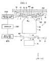
- FIG. 1is an outline configuration drawing showing a first embodiment of an exposure apparatus of the present invention.
- FIG. 2is an enlarged drawing of a main part of FIG. 1 and is a sectional side view showing a liquid immersion unit and its vicinity.
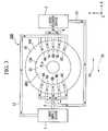
- FIG. 3is a plan view of the liquid immersion unit of FIG. 2 viewed from above.
- FIG. 4is a plan view showing another liquid immersion unit embodiment.
- FIG. 5is an enlarged main part drawing showing a second embodiment of an exposure apparatus of the present invention.
- FIG. 6is a plan view of the liquid immersion unit of FIG. 1 viewed from above.
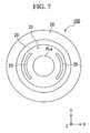
- FIG. 7is a plan view showing another liquid immersion unit embodiment.
- FIG. 8is a flowchart showing an example of a semiconductor device manufacturing process.
- FIG. 1is an outline configuration drawing showing a first embodiment of an exposure apparatus of the present invention.
- an exposure apparatus EXis provided with a mask stage MST that holds a mask M, a substrate stage PST that holds a substrate P, an illumination optical system IL that illuminates the mask M held by the mask stage MST with exposure light EL, a projection optical system PL that projects a pattern image of the mask M illuminated with the exposure light EL onto the substrate P held by the substrate stage PST, and a controller CONT that controls the overall operation of the exposure apparatus EX.
- the projection optical system PLis configured to form an image plane thereabove.
- the mask stage MST that holds the mask Mis disposed under the projection optical system PL, and on the other hand, the substrate stage PST that holds the substrate P is disposed above the projection optical system PL.
- the exposure apparatus EX of the embodimentis a liquid immersion type exposure apparatus to which a liquid immersion method is applied, with the exposure wavelength being shortened in effect, to improve the resolution and at the same time to widen the depth of focus and is provided with a liquid immersion unit 100 constituting a part of a liquid immersion device that fills at least a portion of the space between the projection optical system PL and the substrate P.
- the liquid immersion unit 100is provided with a liquid bath 10 that is fixed to the upper end portion on the image plane side of projection optical system PL, a liquid supply device 1 that supplies liquid 30 via a supply pipe 3 forming a flow path to the liquid bath 10 , and a liquid recovery device 2 that recovers the liquid via a recovery pipe 4 forming a flow path of the liquid from the liquid bath 10 .
- the exposure apparatus EXat least while transferring the pattern image of the mask M onto the substrate P, at least a portion of the space between the projection optical system PL and the substrate P is filled with the liquid 30 supplied from the liquid supply device 1 of the liquid immersion unit 100 and a liquid immersion region AR 2 is formed so as to include the projection area AR 1 of the projection optical system PL.
- the space between the optical element PLa located at the upper end portion of the projection optical system PL and the exposure surface (top surface) of the substrate Pis filled with the liquid 30 , and the pattern image of the mask M is projected onto the substrate P via the projection optical system PL and the liquid 30 between the projection optical system PL and the substrate P, and thus the substrate P is exposed.
- scanning stepperthe exposure apparatus EX in which the substrate P is exposed with the pattern formed on the mask M while synchronously moving the mask M and the substrate P in mutually different directions (opposite directions) along the scanning direction.
- the direction that coincides with the optical axis AX of the projection optical system PLis referred to as the Z-axis direction
- the synchronous movement direction (the scanning direction), in a plane perpendicular to the Z-axis direction, of the mask M and the substrate Pis referred to as the X-axis direction
- the direction perpendicular to the Z-direction and to the Y-directionis referred to as the Y-direction (the non-scanning direction).
- the direction around the X-axis, the direction around the Y-axis, and the direction around the Z-axisare respectively referred to as the ⁇ X-direction, the ⁇ Y-direction, and the ⁇ Z-direction.
- the “substrate” referred to hereinincludes a semiconductor wafer over which a photoresist, a photosensitive material, is coated and that the “mask” includes a reticle formed with a device pattern to be reduction projected onto a substrate.
- the illumination optical system ILis for illuminating the mask M held by the mask stage MST with the exposure light EL and comprises an exposure light source, an optical integrator for uniforming the illuminance of a light flux emitted from the exposure light source, a condenser lens for condensing the exposure light EL from the optical integrator, a relay lens system, a variable field stop for setting an illumination area on the mask M formed by the exposure light EL to be of a slit-like shape, etc.
- a predetermined illumination area on the mask Mis illuminated, by the illumination optical system IL, with the exposure light EL having a uniform illuminance distribution.
- a bright line of ultraviolet regionemitted from the illumination optical system IL
- a deep ultraviolet lightemitted from a mercury lamp
- a deep ultraviolet lightemitted from a mercury lamp
- a deep ultraviolet lightemitted from a mercury lamp
- a deep ultraviolet lightemitted from a mercury lamp
- a deep ultraviolet lightemitted from a mercury lamp
- a deep ultraviolet lightemitted from a mercury lamp
- a deep ultraviolet lightsuch as a KrF excimer laser light (wavelength of 248 nm)
- a vacuum ultraviolet lightVUV light
- an ArF excimer laser lightis used.
- the mask stage MSTis for supporting the mask M, is disposed under the projection optical system PL, and is two-dimensionally movable and finely rotatable in the ⁇ Z-direction, in a plane perpendicular to the optical axis AX, i.e., in the XY-plane.
- vacuum suction holesfor vacuum sucking mask M.
- the mask Mis sucked by and held on the mask stage MST via the vacuum suction holes so that the pattern surface of the mask M is directed upwardly (in the +Z direction).
- the mask MSTis driven by mask stage driving unit MSTD such as a linear motor.
- the mask stage driving unit MSTDis controlled by the controller CONT.
- the mask stage MSTis provided with a moving mirror 50 . Further, a laser interferometer 51 is positioned at a position facing the moving mirror 50 . The two-dimensional position and the rotation angle of the mask M held by the mask stage MST are measured by the laser interferometer 51 in real time, and the measurement results are outputted to the controller CONT. By driving the mask stage driving unit MSTD based on the measurement results from the laser interferometer 51 , the controller CONT performs positioning of the mask M held by the mask stage MST.
- the projection optical system PLis for projection exposing the pattern of the mask M onto the substrate P at a predetermined projection magnification of ⁇ .
- the projection optical system PLis constituted by a plurality of optical elements, including an optical element (lens) PLa disposed at the substrate P side upper end portion, and those optical elements are supported by a lens barrel PK. And, the projection optical system PL is arranged such that it forms thereabove an image plane.
- the projection optical system PLis a reduction system of which projection magnification ⁇ is, e.g., 1 ⁇ 4 or 1 ⁇ 5. It should be noted that the projection optical system PL may also be either a 1 ⁇ magnification system or a magnifying system.
- optical element PLa at the upper end portion of the projection optical system PL of the embodimentis detachable (exchangeable) relative to the lens barrel PK, and the liquid 30 of the liquid immersion region AR 2 is in contact with the optical element PLa.
- the liquid contact surface of the optical element PLais a plane substantially parallel to the XY-plane.
- the substrate stage PST constituting a part of a substrate moving deviceis movable while holding substrate P.
- the substrate stage PSTis provided with a Z stage 52 that holds substrate P via a substrate holder, a XY stage 53 that supports the Z stage 52 , and a base 54 that supports the XY stage 53 .
- the base 54is supported by a supporting member different from a supporting member that supports, e.g., the projection optical system PL.
- the substrate holder of the substrate stage PSTholds the substrate P so that the substrate P's exposure surface that is coated with a photosensitive material and is to be exposed is directed downwardly (in the ⁇ Z direction).
- On the surface (under surface) of the substrate holderare provided a plurality of vacuum suction holes that communicate with a vacuum device.
- the substrate holdersucks and holds the substrate P via the vacuum suction holes.
- the substrate stage PSTis driven by the substrate stage driving unit PSTD such as a linear motor.
- the substrate stage driving unit PSTDis controlled by the controller CONT.
- the Z stage 52By driving the Z stage 52 , the Z-direction position (focus position) and the ⁇ X-direction and ⁇ Y-direction positions of the substrate P held by the Z stage 52 are controlled.
- the XY stage 53By driving the XY stage 53 , the XY-direction position (the position in the direction substantially parallel to the image plane of the projection optical system PL) of the substrate P is controlled.
- the Z stage 52by controlling the focus position and inclination angle of the substrate P, makes the surface of the substrate P to coincide with the image plane of the projection optical system PL in an auto-focus manner and an auto-leveling manner, the XY stage 53 performs positioning of the substrate P in the X-axis and Y-axis directions.
- the Z stage and the XY stagemay be integrally constructed.
- the substrate stage PST(Z stage 52 ) is provided with a moving mirror 55 . Further, a laser interferometer 56 is positioned at a position facing the moving mirror 55 . The two-dimensional position and the rotation angle of the substrate P held by the substrate stage PST are measured by the laser interferometer 56 in real time, and the measurement results are outputted to the controller CONT. By driving the substrate stage driving unit PSTD based on the measurement results from the laser interferometer 56 , the controller CONT performs positioning of the substrate P held by the substrate stage PST.
- FIG. 2is an enlarged drawing of a main part of FIG. 1 and is a sectional side view showing the liquid immersion unit 100 .
- the liquid immersion unit 100is provided with the liquid bath 10 that has a side wall portion 10 C and can hold the liquid 30 , the liquid supply device 1 that supplies the liquid 30 to the liquid bath 10 via the supply pipe 3 , and the liquid recovery device 2 that recovers the liquid 30 via the recovery pipe 4 .
- the liquid supply device 1is provided with a tank that stores the liquid 30 , a compressing pump, etc. and supplies the liquid 30 to the liquid bath 10 via the supply pipe 3 .
- the liquid supply operation of the liquid supply device 1is controlled by the controller CONT.
- the controller CONTcan control the per-unit-time liquid supply amount to the liquid bath 10 of the liquid supply device 1 .
- the liquid supply device 1is provided with a temperature adjusting device that adjusts the temperature of the liquid 30 to be supplied to the liquid bath 10 . By using the temperature adjusting device, the liquid supply device 1 sets the temperature of the liquid 30 to be supplied to the liquid bath 10 to be, for example, substantially the same temperature as that inside a chamber in which the exposure apparatus EX is accommodated.
- the supply pipe 3is provided with a rectifying members 5 for rectifying the liquid 30 to be supplied to the liquid bath 10 .
- the rectifying members 5are constituted by, e.g., a porous material or a slit member having a slit-shaped flow path.
- the liquid supply device 1may be provided with a gas bubble removal device (a degas unit) that removes gas bubbles contained in the liquid 30 to be supplied to the liquid bath 10 .
- the gas bubble removal devicecan be constructed by, for example, a heating device that removes the gas bubbles by heating the liquid 30 or a decompressing unit in which the liquid 30 is stored in a predetermined a container and, by reducing the pressure inside the container, the gas bubbles are removed.
- purified wateris used as the liquid 30 .
- the purified watercan transmit not only ArF excimer laser light, but also the exposure light EL even when it is, for example, a bright line of ultraviolet region (g-line, h-line, or i-line) emitted from a mercury lamp or deep ultraviolet light (DUV light) such as KrF excimer laser light (wavelength of 248 nm).
- a bright line of ultraviolet regiong-line, h-line, or i-line
- DUV lightdeep ultraviolet light
- the liquid recovery device 2is for recovering the liquid 30 in the liquid bath 10 , is provided with, e.g., a suction device such as a vacuum pump, a tank that stores the recovered liquid 30 , etc.
- the liquid recovery device 2recovers the liquid 30 in the liquid bath 10 via the recovery pipe 4 .
- the liquid recovery operation of the liquid recovery device 2is controlled by the controller CONT, and the controller CONT can control the per-unit-time liquid recovery amount of the liquid recovery device 2 .
- the liquid bath 10is for holding the liquid 30 .
- the liquid bath 10has the side wall portion 10 c , and is attached to the upper end portion of the lens barrel of the projection optical system PL.
- On the top portion of the liquid bath 10is formed an opening portion 10 A, and the liquid 30 held by the liquid bath 10 is exposed toward the outside of the liquid bath 10 via the opening portion 10 A.
- the size of the opening portion 10 Ais formed to be larger than that of the projection area AR 1 of the projection optical system PL.
- a bottom portion 10 D of the liquid bath 10is formed a through-hole 10 B.
- the lens barrel upper portion (not shown) of the projection optical system PLInto the through-hole 10 B of the liquid bath 10 is fitted the lens barrel upper portion (not shown) of the projection optical system PL, and between the through-hole 10 B and the lens barrel is provided a sealing member for preventing leakage of the liquid 30 in the liquid bath 10 .
- the upper end surface of the optical element PLa of the projection optical system PLis positioned to be lower than the upper end surface of the side wall portion 10 c of the liquid bath 10 ; and thus, it is configured such that when the liquid bath 10 is filled with liquid 30 , the upper end portion including the upper end surface of the optical element PLa is immersed in the liquid 30 .
- the liquid bath 10is formed by, e.g., a ceramic material. Such a ceramic material, even if a part thereof elutes into the liquid 30 , hardly affects the photosensitive material coated on the exposure surface of the substrate P.
- the substrate stage PSTis configured such that the exposure surface of the substrate P held by the stage is located apart from the upper end portion of the liquid bath 10 by a predetermined distance. More specifically, the distance between the substrate P and the liquid bath 10 is set such that the exposure surface of the substrate P and the liquid 30 exposed upwardly from the opening portion 10 A of the liquid bath 10 come into contact with each other through the surface tension of the liquid 30 .
- FIG. 3is a view of the liquid immersion unit 100 viewed from above.
- the upper end optical element PLa of the projection optical system PLis formed to be circular when viewed from the top, and the liquid bath 10 and its opening portion 10 A are also formed to be circular when viewed from the top.
- the optical element PLais located in substantially the center portion of the liquid bath 10 (the opening portion 10 A).
- the supply pipe 3 connected to the liquid supply device 1branches, halfway, into three flow paths, and each of the branch flow paths is respectively connected to either one of the three supply ports 6 A- 6 C provided on the ⁇ X side of the optical element PLa of the projection optical system PL.
- the optical element PLaOn the +X side of the optical element PLa are provided two recovery ports 7 A and 7 B; and the flow paths, each connected to either one of those recovery ports 7 A and 7 B, are assembled into one, and the assembled flow path is connected to the recovery pipe 4 .
- the supply ports 6 A- 6 C connected to the liquid supply device 1 via the supply pipe 3are provided on the ⁇ X side, and the recovery ports 7 A and 7 B connected to the liquid recovery device 2 via the recovery pipe 4 are provided on the +X side, in a manner in which the upper end portion of the optical element PLa of the projection optical system PL is interposed between the supply ports and the recovery ports.
- supply ports 8 A- 8 C and recovery ports 9 A and 9 Bare disposed in the arrangement in which the supply ports 6 A- 6 C and the recovery ports 7 A and 7 B are rotated by substantially 180 degrees.
- the supply ports 8 A- 8 Care connected to the liquid supply device 1 via the supply pipe 11
- the recovery ports 9 A and 9 Bare connected to the liquid recovery device 2 via the recovery pipe 12 .
- the supply ports 6 A- 6 C and the recovery ports 9 A and 9 Bare disposed alternately in the Y-direction
- the supply ports 8 A- 8 C and the recovery ports 7 A and 7 Bare disposed alternately in the Y-direction.
- the supply and the recovery of the liquid 30are performed by the liquid supply device 1 and the liquid recovery device 2 , by the use of the supply pipe 3 , the supply ports 6 A- 6 C, the recovery pipe 4 , and the recovery ports 7 A and 7 B.
- the liquid 30is supplied from the liquid supply device 1 to the liquid bath 10 including the space between the projection optical system PL and substrate P via the supply pipe 3 and the supply ports 6 A- 6 C, and, at the same time, the liquid 30 is recovered by the liquid recovery device 2 via the recovery ports 7 A and 7 B and the recovery pipe 4 , with the liquid 30 flowing in the +X direction in liquid bath 10 .
- the supply and the recovery of the liquid 30are performed by the liquid supply device 1 and the liquid recovery device 2 , by the use of the supply pipe 11 , the supply ports 8 A- 8 C, the recovery pipe 12 , and the recovery ports 9 A and 9 B.
- the liquid 30is supplied from the liquid supply device 1 to the liquid bath 10 including the space between the projection optical system PL and the substrate P via the supply pipe 11 and the supply ports 8 A- 8 C, and, at the same time, the liquid 30 is recovered by the liquid recovery device 2 via the recovery ports 9 A and 9 B and the recovery pipe 12 , with the liquid 30 flowing in the ⁇ X direction in the liquid bath 10 .
- the controller CONTby using the liquid supply device 1 and the liquid recovery device 2 , makes liquid 30 flow along the moving direction of the substrate P and in the same direction as the moving direction of the substrate P.
- fresh and clean liquid 30can be continuously supplied to the space between the projection optical system PL and the substrate P.
- the space between the projection optical system PL and the substrate Pcan be filled with the liquid 30 , both in of the case where the substrate P is scanned in the +X direction and in the case where the substrate P is scanned in the ⁇ X direction, which makes it possible to obtain a high resolution and a wide depth of focus.
- the liquid bath 10may be attached, for example, a focus detection system that can detect the surface position of the substrate P relative to the image plane of the projection optical system PL.
- the focus detection lightpasses through the liquid 30 .
- the exposure apparatus EX of the present embodimentprojection-exposes the pattern image of the mask M onto the substrate P while moving mask M and substrate P in the X-direction (scanning direction); and, during scanning exposure, a pattern image of a part of the mask M is projected onto the projection area AR 1 formed above the projection optical system PL, and in synchronization with the movement of the mask M in the ⁇ X direction (or in the +X direction) at speed V, the substrate P moves, via the XY stage 53 , in the +X direction (or in the ⁇ X direction) at speed ⁇ V ( ⁇ is the projection magnification). And, after completion of exposure for one shot area, a next shot area is brought to the projection area through the stepping movement of the substrate P, and in this way, exposure for each shot area is successively performed through the step-and-scan method.
- the controller CONTdrives the liquid supply device 1 and the liquid recovery device 2 and starts the supply and recovery operations of the liquid 30 relative to the liquid bath 10 .
- Liquid 30 delivered from the liquid supply device 1 to form the liquid immersion region AR 2after flowing through the supply pipe 3 , is supplied to the liquid bath 10 via the supply ports 6 A- 6 C.
- the controller CONTilluminates the mask M with the exposure light EL by means of the illumination optical system IL while synchronously moving the mask M and the substrate P and projects the pattern image of the mask M onto the substrate P via the projection optical system PL and the liquid 30 .
- the liquid supply device 1 and the liquid recovery device 2While performing scanning exposure with the substrate P being moved in, e.g., the +X-direction, the liquid supply device 1 and the liquid recovery device 2 continue to perform the liquid supply operation and the liquid recovery operation. Since, by doing so, the temperature-adjusted liquid 30 is always supplied from the liquid supply device 1 to the liquid bath 10 , excessive temperature change (temperature rise) of the liquid 30 in liquid bath 10 due to the irradiation heat of the exposure light can be suppressed, which realizes a high accuracy exposure of the pattern image.
- the liquid 30flows, between the substrate P and the optical element PLa of the projection optical system PL, in the direction parallel to (in the same direction as) the scanning direction of the substrate P. Further, when the liquid supply operation by the liquid supply device 1 and the liquid recovery operation by the liquid recovery device 2 are performed in a coordinated manner, the exposure surface of the substrate P and the surface of liquid 30 exposed upwardly from the aperture portion 10 A of the liquid bath 10 come into contact with each other with the aid of the surface tension of liquid 30 , and thus the liquid 30 is disposed between the projection area AR 1 on the substrate P and the optical element PLa, forming the liquid immersion region AR 2 .
- the substrate Pis exposed in the state in which the substrate P is held by the substrate stage PST such that the exposure surface of the substrate P comes into contact with the surface of liquid 30 .
- the substrate stage PSTcan freely move the substrate P in the XY-plane, with the substrate not being in contact with liquid bath 10 .
- the controller CONTmay change, depending on the scanning speed of the substrate P, the per-unit-time liquid supply amount of the liquid supply device 1 and the per-unit-time liquid recovery amount of the liquid recovery device 2 .
- the per-unit-time liquid supply amount and the per-unit-time liquid recovery amountare increased.
- the flow rate of liquid 30 flowing between the projection optical system PL and the substrate Palso increases in accordance with the moving speed of the substrate P, and thus the liquid immersion region AR 2 can be smoothly formed between the projection optical system PL and the substrate P.
- the size of the liquid bath 10is determined in accordance with the moving speed of the substrate P. More specifically, when the moving speed of the substrate P is made to be higher, there arises the possibility that the liquid 30 in the liquid bath 10 is dragged by substrate P, the formation of the liquid immersion region AR 2 becomes unstable, and the liquid 30 cannot be disposed on the projection area AR 1 on the substrate P, though the liquid 30 can be, by making the liquid bath 10 larger to make the area of the contact surface between the substrate P and the liquid 30 larger, smoothly disposed on the projection area AR 1 , even if the moving speed of the substrate P is made to be higher.
- the distance between the liquid bath 10 and the substrate P held by substrate stage PSTmay be determined in accordance with the surface tension (interfacial tension) of the liquid 30 to be used.
- Purified wateris used as liquid 30 in the embodiment; but, when another kind of liquid is used, since the surface tension values (interfacial tension values) of liquids vary depending on their material characteristics, the distance between the liquid bath 10 and the substrate P is set in accordance with the surface tension of the liquid used.
- the liquid bath 10 of the liquid immersion unit 100can be provided on the upper end portion of the projection optical system PL that does not move, and the liquid immersion region AR 2 can be formed between the projection optical system PL and the substrate P. Since the position of the liquid bath 10 is fixed, the undulation of the liquid surface exposed upwardly from the aperture portion 10 A of the liquid bath 10 and the scattering of the liquid can be prevented, and the deterioration of the pattern image projected onto the substrate P can be suppressed.
- the liquid supply device 1 for supplying liquid 30 to form the liquid immersion region AR 2 and the supply pipe 3 connected thereto, and the liquid recovery device 2 for recovering liquid 30 and the recovery pipe 4 connected theretoneed not be attached to the substrate stage PST which is a moving portion, the disadvantage, due to the device and the pipes, that the movement of the substrate stage PST is disturbed can be suppressed, for example.
- the liquid immersion exposurecan also be performed in the state that the liquid 30 is, without being made to flow, pooled in the liquid bath 10 .
- occurrence of temperature change (temperature rise) of liquid 30 in the liquid bath 10 due to the exposure light irradiation heatcan be suppressed, and deterioration of the pattern can be prevented.
- clean liquid 30can be always supplied from the liquid supply device 1 to the liquid bath 10 , and, at the same time, even if impurities have come to be mixed in the liquid 30 of the liquid bath 10 , the impurities can be immediately recovered from the liquid bath 10 by the liquid recovery device 2 .
- each of the Y-direction side portions between which the optical element PLa of the projection optical system PL is interposedmay be provided supply nozzles 13 A- 13 C, supply nozzles 14 A- 14 C, recovery nozzles 15 A, 15 B, 16 A, and 16 B.
- the liquid bath 10is attached to the lens barrel in the vicinity of the upper end portion of the projection optical system PL, it may also be configured such that the bath is held by a supporting member separated from the projection optical system PL.
- FIG. 5is a sectional side view of liquid immersion unit 100 of the second embodiment
- FIG. 6is a plan view thereof viewed from above.
- the same or equivalent constituent elements as those in the above-described embodimentare denoted by the same reference numerals, and their descriptions will be abridged or omitted.
- the liquid immersion unit 100is provided with a liquid immersion forming member 20 that is attached to the upper end portion optical element PLa of the projection optical system PL and has an upper surface 21 facing the substrate P, with liquid supply ports 23 A- 23 C that formed on the upper surface 21 and are connected to the liquid supply device 1 via flow paths 22 A- 22 C formed inside the forming member 20 and supply pipe 3 , and with liquid recovery ports 25 A and 25 B that formed on the upper surface 21 and are connected to the liquid recovery device 2 via flow paths 24 A and 24 B and recovery pipe 4 .
- the forming member 20has, in its center portion, as viewed from the top, a hole portion 20 A that fits with the optical element PLa of the projection optical system PL, and it is configured such that when the optical element PLa is fitted with the hole portion 20 A, the upper surface 21 of the forming member 20 and the upper end surface of the optical element PLa of the projection optical system PL are substantially flush with each other.
- Each of the liquid supply ports 23 A- 23 Cis provided on the ⁇ X side of the optical element PLa of the projection optical system PL and discharges the liquid 30 upwardly.
- the liquid recovery ports 25 A and 25 Bare provided on the +X side of the optical element PLa and suck the liquid 30 downwardly.
- liquid supply ports and two liquid recovery portsare provided with, the number and arrangement thereof may be set in a discretionary way. Further, as well as the first embodiment, separate liquid supply ports and liquid recovery ports may be provided on the upper surface 21 in the arrangement in which the above-described liquid supply ports 23 A- 23 C and liquid recovery ports 25 A and 25 B are rotated by substantially 180 degrees.
- trap portions 28 and 29that recover liquid 30 that has not been recovered by the liquid recovery ports.
- Each of the trap portions 28 and 29is an arc-shaped groove, as viewed from the top, and is provided in the position such that the optical element PLa of the projection optical system PL is interposed between the trap portions.
- a flow path 30 connected to the trap portion 29is connected to a tank 32 and to a vacuum pump 34 as a suction device, via a conduit 31 provided outside the forming member 20 .
- the flow path that connects the tank 32 with the vacuum pump 34is provided with a valve 33 .
- the tank 32is provided with a discharge flow path 32 A, and it is configured such that when the liquid 30 has pooled in the tank up to a predetermined amount, the liquid is discharged through the discharge flow path 32 A.
- a flow path 35 connected to the trap portion 28is also connected to a tank, a valve, and a vacuum pump, similar to the above-described ones.
- the controller CONTdrives the liquid supply device 1 and the liquid recovery device 2 , supplies the liquid 30 to the upper surface 21 via the liquid supply ports 23 A- 23 C, and forms the liquid immersion region AR 2 between the optical element PLa of the projection optical system PL and the substrate P. And, the liquid 30 is recovered via the liquid recovery ports 25 A and 25 B, and the substrate P is exposed, with liquid 30 being made to flow in the direction parallel to (in the same direction as) the scanning direction of the substrate P.
- the liquid 30 supplied from, e.g., the liquid supply device 1 via supply ports 23 A- 23 Cflows in the manner that the liquid, being induced by the +X direction movement of the substrate P, is pulled into the space between the projection optical system PL and the substrate P, and thus, even if the supply energy of the liquid supply device 1 is small, the temperature-adjusted liquid 30 is always supplied from the liquid supply device 1 between the upper end surface of the optical element PLa and the substrate P, and excessive temperature change (temperature rise) of the liquid 30 due to the irradiation heat of the exposure light is suppressed, which realizes a high accuracy exposure of the pattern image.
- the liquid bath having the side wallis used to hold the liquid 30 in the first embodiment; in contrast, it is configured in the second embodiment such that the liquid 30 is disposed between the planar upper surface 21 and the upper end surface of the optical element PLa, and the substrate P, and thus, even when the substrate P is inclined by a large amount, the substrate P does not come into contact with the forming member 20 . And, since, also in this embodiment, it is configured such that the substrate P is moved in the state that the liquid immersion forming member 20 of the liquid immersion unit 100 is fixed to the projection optical system PL that does not move, undulation, scattering, etc. of the liquid 30 do not occur, which realizes stable projection of the pattern image onto the substrate P.
- the trap portion 28may be formed annularly so as to surround the optical element PLa of the projection optical system PL. Still further, it may be configured such that, without providing the liquid recovery ports 25 A and 25 B, all of the supplied liquid 30 is recovered by the trap portions 28 and 29 .
- the trap portions for recovering the liquid 30 that has not been recovered by the liquid recovery portsare constituted by the grooves and the vacuum pumps (suction devices) connected thereto, but, by, for example, disposing porous members, such as sponges, in the grooves, the liquid 30 that has not been recovered can be recovered and held by the porous members.
- the liquid 30 of the embodimentsis constituted by purified water.
- Purified waterhas the advantage that it can be easily available in large quantities in, e.g., a semiconductor manufacturing factories and also the advantage that it does not adversely affect photoresist on the substrate P, the optical elements (lenses), etc. Further, purified water does not adversely affect the environment and contains scarcely any impurities. Thus, the effect that it cleans the surface of the substrate P and the surface of the optical element provided at the end portion of the projection optical system PL can be expected.
- the refractive index n of purified water (water) relative to the exposure light EL having a wavelength of about 193 nmis approximately 1.44, and when ArF excimer laser light (having 193 nm wavelength) is used as the light source of exposure light EL, the wavelength is effectively shortened, on the substrate P, as multiplied by 1/n, i.e., effectively becomes approximately 134 nm, and thus, a high resolution can be obtained.
- the numerical aperture of the projection optical system PLcan be further increased if it is preferable to ensure a depth of focus approximately the same as that when used in air, and the resolution is also improved from this standpoint.
- the pressure, caused by the flow of the liquid 30 , of the space between the optical element located at the end of the projection optical system PL and the substrate Pis high, it may be configured such that the optical element is rigidly fixed so as not to move due to the pressure, instead of making the optical element exchangeable.
- the liquid 30is water
- the liquid 30may be a liquid other than water.
- the light source of the exposure light ELis an F 2 laser
- the F 2 laser lightdoes not transmit through water, and thus, as the liquid 30 , a fluorofluid that can transmit the F 2 laser light may be used.
- a materiale.g., cedar oil
- cedar oile.g., cedar oil
- the substrate P of each of the above-described embodimentscan be not only a semiconductor wafer for manufacturing a semiconductor device, but also a glass substrate for a display device, a ceramic wafer for a thin film magnetic head, a master mask or reticle (synthetic quartz or silicon wafer), etc.
- the exposure apparatus EXin addition to a scan type exposure apparatus (scanning stepper) in which while synchronously moving the mask M and the substrate P, the pattern of the mask M is scan-exposed, a step-and-repeat type projection exposure apparatus (stepper) that exposes the full pattern of the mask M in the state in which the mask M and substrate P are stationary, and the substrate P is successively moved stepwise can be used. Also, the present invention can be applied to a step-and-stitch type exposure apparatus in which at least two patterns are transferred onto the substrate P in a partially overlapping manner.
- the present inventioncan be applied to a twin stage type exposure apparatus, which is disclosed in, e.g., Japanese Unexamined Patent Application, First Publication Nos. H10-163099 and H10-214783, and Published Japanese Translation No. 2000-505958 of the PCT International Publication.
- the type of exposure apparatus EXis not limited to an exposure apparatus, which exposes a semiconductor pattern onto the substrate P, for manufacturing semiconductor devices, but can also be applied to a variety of exposure apparatuses, e.g., an exposure apparatus for manufacturing liquid crystal display devices or a displays, an exposure apparatus for manufacturing thin film magnetic heads, an exposure apparatus for manufacturing image pickup devices, and an exposure apparatus for manufacturing reticles or masks.
- each of substrate stage PST and mask stage MSTmay be either of a type moving along a guide or of a guideless type having no guide.
- a planar motormay be used that opposes a magnet unit in which magnets are two-dimensionally arranged to an armature unit in which coils are two-dimensionally arranged, and that drives each of the substrate stage PST and the mask stage MST by an electromagnetic force.
- either one of the magnet unit and the armature unitis attached to the stage PST or the stage MST, and the other unit is attached to the moving surface side of the stage PST or the stage MST.
- a reaction force generated by the movement of the substrate stage PSTmay be, as described in Japanese Unexamined Patent Application, First Publication No. H08-166475 (U.S. Pat. No. 5,528,118), mechanically released to the floor (earth) by use of a frame member so that the force does not transmit to the projection optical system PL.
- a reaction force generated by the movement of the mask stage MSTmay be, as described in Japanese Unexamined Patent Application, First Publication No. H08-330224 (U.S. patent application Ser. No. 08/416,558), mechanically released to the floor (earth) by use of a frame member so that the force does not transmit to the projection optical system PL.
- the exposure apparatus EXis built by assembling various subsystems, including each element listed in the claims of the present application, in such a manner that prescribed mechanical accuracy, electrical accuracy, and optical accuracy are maintained.
- every optical systemis adjusted to achieve its optical accuracy
- every mechanical systemis adjusted to achieve its mechanical accuracy
- every electrical systemis adjusted to achieve its electrical accuracy.
- the process of assembling each subsystem into the exposure apparatusincludes mechanical interfaces, electrical circuit wiring connections, and air pressure plumbing connections between each subsystem. Needless to say, there is also a process where each subsystem is assembled prior to the assembling of the exposure apparatus from the various subsystems.
- micro devicessuch as semiconductor devices are manufactured by a series of steps, including: step 201 in which the micro device's function and performance design is performed; step 202 in which a mask (reticle) is manufactured based on the design step; step 203 in which a substrate, the device's base material, is manufactured; step 204 in which the mask pattern is exposed onto the substrate by the exposure apparatus EX according to the above-described embodiments; device assembly step 205 (including the dicing process, bonding process, and packaging process); inspection step 206 .
- step 201in which the micro device's function and performance design is performed
- step 202in which a mask (reticle) is manufactured based on the design step
- step 203in which a substrate, the device's base material, is manufactured
- step 204in which the mask pattern is exposed onto the substrate by the exposure apparatus EX according to the above-described embodiments
- device assembly step 205including the dicing process, bonding process, and packaging process
- inspection step 206inspection step 206 .
Landscapes
- Physics & Mathematics (AREA)
- General Physics & Mathematics (AREA)
- Exposure And Positioning Against Photoresist Photosensitive Materials (AREA)
- Exposure Of Semiconductors, Excluding Electron Or Ion Beam Exposure (AREA)
- Control Of Vending Devices And Auxiliary Devices For Vending Devices (AREA)
- Liquid Crystal (AREA)
Abstract
Description
R=k1·λ/NA, (1)
δ=±k2·λ/NA2, (2)
where λ is the exposure wavelength, NA is the numerical aperture of the projection optical system, and k1and k2are process coefficients. It can be seen from formulas (1) and (2) that if, to enhance the resolution R, the wavelength λ is made shorter and the numerical aperture is made larger, then the depth of focus δ becomes narrower.
Claims (11)
Priority Applications (1)
| Application Number | Priority Date | Filing Date | Title |
|---|---|---|---|
| US11/600,763US8111375B2 (en) | 2003-04-07 | 2006-11-17 | Exposure apparatus and method for manufacturing device |
Applications Claiming Priority (6)
| Application Number | Priority Date | Filing Date | Title |
|---|---|---|---|
| JP2003103145 | 2003-04-07 | ||
| JP2003-103145 | 2003-04-07 | ||
| PCT/JP2004/004969WO2004090956A1 (en) | 2003-04-07 | 2004-04-06 | Exposure apparatus and method for manufacturing device |
| US11/239,402US7480029B2 (en) | 2003-04-07 | 2005-09-30 | Exposure apparatus and method for manufacturing device |
| US11/257,089US20060033901A1 (en) | 2003-04-07 | 2005-10-25 | Exposure apparatus and method for manufacturing device |
| US11/600,763US8111375B2 (en) | 2003-04-07 | 2006-11-17 | Exposure apparatus and method for manufacturing device |
Related Parent Applications (1)
| Application Number | Title | Priority Date | Filing Date |
|---|---|---|---|
| US11/257,089ContinuationUS20060033901A1 (en) | 2003-04-07 | 2005-10-25 | Exposure apparatus and method for manufacturing device |
Publications (2)
| Publication Number | Publication Date |
|---|---|
| US20070064209A1 US20070064209A1 (en) | 2007-03-22 |
| US8111375B2true US8111375B2 (en) | 2012-02-07 |
Family
ID=33156817
Family Applications (4)
| Application Number | Title | Priority Date | Filing Date |
|---|---|---|---|
| US11/239,402Expired - Fee RelatedUS7480029B2 (en) | 2003-04-07 | 2005-09-30 | Exposure apparatus and method for manufacturing device |
| US11/257,089AbandonedUS20060033901A1 (en) | 2003-04-07 | 2005-10-25 | Exposure apparatus and method for manufacturing device |
| US11/600,763Expired - Fee RelatedUS8111375B2 (en) | 2003-04-07 | 2006-11-17 | Exposure apparatus and method for manufacturing device |
| US12/219,835Expired - Fee RelatedUS8537331B2 (en) | 2003-04-07 | 2008-07-29 | Exposure apparatus and method for manufacturing device |
Family Applications Before (2)
| Application Number | Title | Priority Date | Filing Date |
|---|---|---|---|
| US11/239,402Expired - Fee RelatedUS7480029B2 (en) | 2003-04-07 | 2005-09-30 | Exposure apparatus and method for manufacturing device |
| US11/257,089AbandonedUS20060033901A1 (en) | 2003-04-07 | 2005-10-25 | Exposure apparatus and method for manufacturing device |
Family Applications After (1)
| Application Number | Title | Priority Date | Filing Date |
|---|---|---|---|
| US12/219,835Expired - Fee RelatedUS8537331B2 (en) | 2003-04-07 | 2008-07-29 | Exposure apparatus and method for manufacturing device |
Country Status (8)
| Country | Link |
|---|---|
| US (4) | US7480029B2 (en) |
| EP (1) | EP1612850B1 (en) |
| JP (2) | JP4902201B2 (en) |
| KR (1) | KR101176817B1 (en) |
| AT (1) | ATE426914T1 (en) |
| DE (1) | DE602004020200D1 (en) |
| TW (1) | TWI385706B (en) |
| WO (1) | WO2004090956A1 (en) |
Families Citing this family (63)
| Publication number | Priority date | Publication date | Assignee | Title |
|---|---|---|---|---|
| EP1612850B1 (en)* | 2003-04-07 | 2009-03-25 | Nikon Corporation | Exposure apparatus and method for manufacturing a device |
| KR101547077B1 (en) | 2003-04-09 | 2015-08-25 | 가부시키가이샤 니콘 | Exposure method and apparatus, and device manufacturing method |
| EP2950147B1 (en) | 2003-04-10 | 2017-04-26 | Nikon Corporation | Environmental system including vaccum scavenge for an immersion lithography apparatus |
| EP3062152B1 (en) | 2003-04-10 | 2017-12-20 | Nikon Corporation | Environmental system including vaccum scavenge for an immersion lithography apparatus |
| KR101225884B1 (en)* | 2003-04-11 | 2013-01-28 | 가부시키가이샤 니콘 | Apparatus and method for maintaining immersion fluid in the gap under the projection lens during wafer exchange in an immersion lithography machine |
| EP2261741A3 (en) | 2003-06-11 | 2011-05-25 | ASML Netherlands B.V. | Lithographic apparatus and device manufacturing method |
| US6867844B2 (en) | 2003-06-19 | 2005-03-15 | Asml Holding N.V. | Immersion photolithography system and method using microchannel nozzles |
| TW201721717A (en) | 2003-06-19 | 2017-06-16 | 尼康股份有限公司 | Exposure apparatus, exposure method, and device manufacturing method |
| US6809794B1 (en)* | 2003-06-27 | 2004-10-26 | Asml Holding N.V. | Immersion photolithography system and method using inverted wafer-projection optics interface |
| EP1491956B1 (en)* | 2003-06-27 | 2006-09-06 | ASML Netherlands B.V. | Lithographic apparatus and device manufacturing method |
| WO2005006415A1 (en) | 2003-07-09 | 2005-01-20 | Nikon Corporation | Exposure apparatus and method for manufacturing device |
| US7370659B2 (en) | 2003-08-06 | 2008-05-13 | Micron Technology, Inc. | Photolithographic stepper and/or scanner machines including cleaning devices and methods of cleaning photolithographic stepper and/or scanner machines |
| TWI245163B (en)* | 2003-08-29 | 2005-12-11 | Asml Netherlands Bv | Lithographic apparatus and device manufacturing method |
| EP3223053A1 (en)* | 2003-09-03 | 2017-09-27 | Nikon Corporation | Apparatus and method for providing fluid for immersion lithography |
| TWI573175B (en) | 2003-10-28 | 2017-03-01 | 尼康股份有限公司 | Optical illumination device, exposure device, exposure method and device manufacturing method |
| US7411653B2 (en) | 2003-10-28 | 2008-08-12 | Asml Netherlands B.V. | Lithographic apparatus |
| US7528929B2 (en) | 2003-11-14 | 2009-05-05 | Asml Netherlands B.V. | Lithographic apparatus and device manufacturing method |
| TWI385414B (en) | 2003-11-20 | 2013-02-11 | 尼康股份有限公司 | Optical illuminating apparatus, illuminating method, exposure apparatus, exposure method and device fabricating method |
| JP4323946B2 (en) | 2003-12-19 | 2009-09-02 | キヤノン株式会社 | Exposure equipment |
| US7589822B2 (en) | 2004-02-02 | 2009-09-15 | Nikon Corporation | Stage drive method and stage unit, exposure apparatus, and device manufacturing method |
| TWI389174B (en) | 2004-02-06 | 2013-03-11 | 尼康股份有限公司 | Polarization changing device, optical illumination apparatus, light-exposure apparatus and light-exposure method |
| CN100592210C (en)* | 2004-02-13 | 2010-02-24 | 卡尔蔡司Smt股份公司 | Projection objective lens of microlithographic projection exposure device |
| KR101851511B1 (en) | 2004-03-25 | 2018-04-23 | 가부시키가이샤 니콘 | Exposure apparatus and method for manufacturing device |
| WO2005104195A1 (en) | 2004-04-19 | 2005-11-03 | Nikon Corporation | Exposure apparatus and device producing method |
| US8054448B2 (en) | 2004-05-04 | 2011-11-08 | Nikon Corporation | Apparatus and method for providing fluid for immersion lithography |
| US7304715B2 (en) | 2004-08-13 | 2007-12-04 | Asml Netherlands B.V. | Lithographic apparatus and device manufacturing method |
| US7701550B2 (en) | 2004-08-19 | 2010-04-20 | Asml Netherlands B.V. | Lithographic apparatus and device manufacturing method |
| US7379155B2 (en)* | 2004-10-18 | 2008-05-27 | Asml Netherlands B.V. | Lithographic apparatus and device manufacturing method |
| US7161654B2 (en)* | 2004-12-02 | 2007-01-09 | Asml Netherlands B.V. | Lithographic apparatus and device manufacturing method |
| JP4784513B2 (en) | 2004-12-06 | 2011-10-05 | 株式会社ニコン | Maintenance method, maintenance equipment, exposure apparatus, and device manufacturing method |
| US7180571B2 (en)* | 2004-12-08 | 2007-02-20 | Asml Netherlands B.V. | Lithographic projection apparatus and actuator |
| SG124351A1 (en)* | 2005-01-14 | 2006-08-30 | Asml Netherlands Bv | Lithographic apparatus and device manufacturing method |
| US8692973B2 (en) | 2005-01-31 | 2014-04-08 | Nikon Corporation | Exposure apparatus and method for producing device |
| KR101513840B1 (en) | 2005-01-31 | 2015-04-20 | 가부시키가이샤 니콘 | Exposure apparatus and method for manufacturing device |
| CN102360170B (en) | 2005-02-10 | 2014-03-12 | Asml荷兰有限公司 | Immersion liquid, exposure apparatus, and exposure process |
| US7324185B2 (en) | 2005-03-04 | 2008-01-29 | Asml Netherlands B.V. | Lithographic apparatus and device manufacturing method |
| US7411654B2 (en)* | 2005-04-05 | 2008-08-12 | Asml Netherlands B.V. | Lithographic apparatus and device manufacturing method |
| US20060232753A1 (en) | 2005-04-19 | 2006-10-19 | Asml Holding N.V. | Liquid immersion lithography system with tilted liquid flow |
| US8248577B2 (en) | 2005-05-03 | 2012-08-21 | Asml Netherlands B.V. | Lithographic apparatus and device manufacturing method |
| KR20180128526A (en) | 2005-05-12 | 2018-12-03 | 가부시키가이샤 니콘 | Projection optical system, exposure apparatus and device manufacturing method |
| DE102005024163A1 (en) | 2005-05-23 | 2006-11-30 | Carl Zeiss Smt Ag | Optical system e.g. projection objective, for microlithography projection exposure system, has module insertable and removable as unit into system, and concave curved optical surface for capping cavity during operation of exposure system |
| US7583358B2 (en) | 2005-07-25 | 2009-09-01 | Micron Technology, Inc. | Systems and methods for retrieving residual liquid during immersion lens photolithography |
| US7456928B2 (en) | 2005-08-29 | 2008-11-25 | Micron Technology, Inc. | Systems and methods for controlling ambient pressure during processing of microfeature workpieces, including during immersion lithography |
| JP2007088339A (en)* | 2005-09-26 | 2007-04-05 | Nikon Corp | Exposure apparatus and device manufacturing method |
| JPWO2007055237A1 (en) | 2005-11-09 | 2009-04-30 | 株式会社ニコン | Exposure apparatus, exposure method, and device manufacturing method |
| US20070127002A1 (en)* | 2005-11-09 | 2007-06-07 | Nikon Corporation | Exposure apparatus and method, and device manufacturing method |
| WO2007055199A1 (en) | 2005-11-09 | 2007-05-18 | Nikon Corporation | Exposure apparatus and method, and method for manufacturing device |
| TWI397945B (en) | 2005-11-14 | 2013-06-01 | 尼康股份有限公司 | A liquid recovery member, an exposure apparatus, an exposure method, and an element manufacturing method |
| US7773195B2 (en) | 2005-11-29 | 2010-08-10 | Asml Holding N.V. | System and method to increase surface tension and contact angle in immersion lithography |
| JP5194799B2 (en) | 2005-12-06 | 2013-05-08 | 株式会社ニコン | Exposure method, exposure apparatus, and device manufacturing method |
| US8472004B2 (en) | 2006-01-18 | 2013-06-25 | Micron Technology, Inc. | Immersion photolithography scanner |
| JP4889331B2 (en)* | 2006-03-22 | 2012-03-07 | 大日本スクリーン製造株式会社 | Substrate processing apparatus and substrate processing method |
| US9477158B2 (en)* | 2006-04-14 | 2016-10-25 | Asml Netherlands B.V. | Lithographic apparatus and device manufacturing method |
| US8451427B2 (en) | 2007-09-14 | 2013-05-28 | Nikon Corporation | Illumination optical system, exposure apparatus, optical element and manufacturing method thereof, and device manufacturing method |
| JP5267029B2 (en) | 2007-10-12 | 2013-08-21 | 株式会社ニコン | Illumination optical apparatus, exposure apparatus, and device manufacturing method |
| CN101681125B (en) | 2007-10-16 | 2013-08-21 | 株式会社尼康 | Illumination optical system, exposure apparatus, and device manufacturing method |
| CN101681123B (en) | 2007-10-16 | 2013-06-12 | 株式会社尼康 | Illumination optical system, exposure apparatus, and device manufacturing method |
| US8379187B2 (en) | 2007-10-24 | 2013-02-19 | Nikon Corporation | Optical unit, illumination optical apparatus, exposure apparatus, and device manufacturing method |
| US9116346B2 (en) | 2007-11-06 | 2015-08-25 | Nikon Corporation | Illumination apparatus, illumination method, exposure apparatus, and device manufacturing method |
| CN105606344B (en) | 2008-05-28 | 2019-07-30 | 株式会社尼康 | Lamp optical system, means of illumination, exposure device and exposure method |
| DE102008050868A1 (en)* | 2008-09-30 | 2010-04-08 | M+W Zander Products Gmbh | Fluid i.e. ultra-pure water, temperature stabilizing device for use during manufacturing of chips from silicon wafers, has reservoir lying in flow path of fluid and containing volume of fluid, where supplied fluid passes through reservoir |
| US20110153387A1 (en)* | 2009-12-17 | 2011-06-23 | Google Inc. | Customizing surveys |
| WO2015189875A1 (en)* | 2014-06-12 | 2015-12-17 | 富士電機株式会社 | Impurity adding apparatus, impurity adding method, and semiconductor element manufacturing method |
Citations (130)
| Publication number | Priority date | Publication date | Assignee | Title |
|---|---|---|---|---|
| US3243321A (en) | 1962-11-02 | 1966-03-29 | Atlas Copco Ab | Method of teflon coating of metals |
| US3648587A (en) | 1967-10-20 | 1972-03-14 | Eastman Kodak Co | Focus control for optical instruments |
| US4346164A (en) | 1980-10-06 | 1982-08-24 | Werner Tabarelli | Photolithographic method for the manufacture of integrated circuits |
| JPS57153433A (en) | 1981-03-18 | 1982-09-22 | Hitachi Ltd | Manufacturing device for semiconductor |
| JPS58202448A (en) | 1982-05-21 | 1983-11-25 | Hitachi Ltd | exposure equipment |
| JPS5919912A (en) | 1982-07-26 | 1984-02-01 | Hitachi Ltd | Immersion distance holding device |
| DD221563A1 (en) | 1983-09-14 | 1985-04-24 | Mikroelektronik Zt Forsch Tech | IMMERSIONS OBJECTIVE FOR THE STEP-BY-STEP PROJECTION IMAGING OF A MASK STRUCTURE |
| DD224448A1 (en) | 1984-03-01 | 1985-07-03 | Zeiss Jena Veb Carl | DEVICE FOR PHOTOLITHOGRAPHIC STRUCTURAL TRANSMISSION |
| JPS6265326A (en) | 1985-09-18 | 1987-03-24 | Hitachi Ltd | Exposure device |
| JPS63157419A (en) | 1986-12-22 | 1988-06-30 | Toshiba Corp | Fine pattern transfer apparatus |
| EP0418427A2 (en) | 1989-09-06 | 1991-03-27 | Eiichi Miyake | Exposure process |
| US5059287A (en) | 1989-06-16 | 1991-10-22 | Charles W. Harkey, Sr. | Portable water distiller |
| EP0605103A1 (en) | 1992-11-27 | 1994-07-06 | Canon Kabushiki Kaisha | Projection apparatus for immersed exposure |
| US5528118A (en) | 1994-04-01 | 1996-06-18 | Nikon Precision, Inc. | Guideless stage with isolated reaction stage |
| US5623853A (en) | 1994-10-19 | 1997-04-29 | Nikon Precision Inc. | Precision motion stage with single guide beam and follower stage |
| US5715039A (en) | 1995-05-19 | 1998-02-03 | Hitachi, Ltd. | Projection exposure apparatus and method which uses multiple diffraction gratings in order to produce a solid state device with fine patterns |
| WO1998028665A1 (en) | 1996-12-24 | 1998-07-02 | Koninklijke Philips Electronics N.V. | Two-dimensionally balanced positioning device with two object holders, and lithographic device provided with such a positioning device |
| US5825043A (en) | 1996-10-07 | 1998-10-20 | Nikon Precision Inc. | Focusing and tilting adjustment system for lithography aligner, manufacturing apparatus or inspection apparatus |
| US5874820A (en) | 1995-04-04 | 1999-02-23 | Nikon Corporation | Window frame-guided stage mechanism |
| WO1999049504A1 (en) | 1998-03-26 | 1999-09-30 | Nikon Corporation | Projection exposure method and system |
| JP2000012453A (en)* | 1998-06-18 | 2000-01-14 | Nikon Corp | Exposure apparatus, method of using the same, exposure method, and method of manufacturing mask |
| US20020145714A1 (en) | 2001-04-05 | 2002-10-10 | Nikon Corporation | Reticle chucks and methods for holding a lithographic reticle utilizing same |
| US20020149753A1 (en) | 1997-09-04 | 2002-10-17 | Canon Kabushiki Kaisha | Exposure apparatus and device manufacturing method |
| US20020163629A1 (en) | 2001-05-07 | 2002-11-07 | Michael Switkes | Methods and apparatus employing an index matching medium |
| US20030030916A1 (en) | 2000-12-11 | 2003-02-13 | Nikon Corporation | Projection optical system and exposure apparatus having the projection optical system |
| WO2003077037A1 (en) | 2002-03-08 | 2003-09-18 | Carl Zeiss Smt Ag | Refractive projection objective for immersion lithography |
| US20040000627A1 (en) | 2002-06-28 | 2004-01-01 | Carl Zeiss Semiconductor Manufacturing Technologies Ag | Method for focus detection and an imaging system with a focus-detection system |
| WO2004019128A2 (en) | 2002-08-23 | 2004-03-04 | Nikon Corporation | Projection optical system and method for photolithography and exposure apparatus and method using same |
| US20040075895A1 (en)* | 2002-10-22 | 2004-04-22 | Taiwan Semiconductor Manufacturing Co., Ltd. | Apparatus for method for immersion lithography |
| US20040109237A1 (en) | 2002-12-09 | 2004-06-10 | Carl Zeiss Smt Ag | Projection objective, especially for microlithography, and method for adjusting a projection objective |
| US20040114117A1 (en) | 2002-11-18 | 2004-06-17 | Asml Netherlands B.V. | Lithographic apparatus and device manufacturing method |
| US20040119954A1 (en) | 2002-12-10 | 2004-06-24 | Miyoko Kawashima | Exposure apparatus and method |
| US20040118184A1 (en) | 2002-12-19 | 2004-06-24 | Asml Holding N.V. | Liquid flow proximity sensor for use in immersion lithography |
| US6757051B2 (en) | 2000-06-19 | 2004-06-29 | Nikon Corporation | Projection optical system, manufacturing method thereof, and projection exposure apparatus |
| US20040125351A1 (en) | 2002-12-30 | 2004-07-01 | Krautschik Christof Gabriel | Immersion lithography |
| WO2004055803A1 (en) | 2002-12-13 | 2004-07-01 | Koninklijke Philips Electronics N.V. | Liquid removal in a method and device for irradiating spots on a layer |
| WO2004057589A1 (en) | 2002-12-19 | 2004-07-08 | Koninklijke Philips Electronics N.V. | Method and device for irradiating spots on a layer |
| WO2004057590A1 (en) | 2002-12-19 | 2004-07-08 | Koninklijke Philips Electronics N.V. | Method and device for irradiating spots on a layer |
| US20040136494A1 (en) | 2002-11-12 | 2004-07-15 | Asml Netherlands B.V. | Lithographic apparatus and device manufacturing method |
| US20040160582A1 (en) | 2002-11-12 | 2004-08-19 | Asml Netherlands B.V. | Lithographic apparatus and device manufacturing method |
| US20040165159A1 (en) | 2002-11-12 | 2004-08-26 | Asml Netherlands B.V. | Lithographic apparatus and device manufacturing method |
| US20040169924A1 (en) | 2003-02-27 | 2004-09-02 | Asml Netherlands, B.V. | Stationary and dynamic radial transverse electric polarizer for high numerical aperture systems |
| US20040169834A1 (en) | 2002-11-18 | 2004-09-02 | Infineon Technologies Ag | Optical device for use with a lithography method |
| WO2004077154A2 (en) | 2003-02-21 | 2004-09-10 | Asml Holding N.V. | Lithographic printing with polarized light |
| US20040180299A1 (en) | 2003-03-11 | 2004-09-16 | Rolland Jason P. | Immersion lithography methods using carbon dioxide |
| US20040207824A1 (en) | 2002-11-12 | 2004-10-21 | Asml Netherlands B.V. | Lithographic apparatus and device manufacturing method |
| WO2004090634A2 (en) | 2003-04-10 | 2004-10-21 | Nikon Corporation | Environmental system including vaccum scavange for an immersion lithography apparatus |
| WO2004090577A2 (en) | 2003-04-11 | 2004-10-21 | Nikon Corporation | Maintaining immersion fluid under a lithographic projection lens |
| WO2004090633A2 (en) | 2003-04-10 | 2004-10-21 | Nikon Corporation | An electro-osmotic element for an immersion lithography apparatus |
| US6809794B1 (en) | 2003-06-27 | 2004-10-26 | Asml Holding N.V. | Immersion photolithography system and method using inverted wafer-projection optics interface |
| WO2004093159A2 (en) | 2003-04-09 | 2004-10-28 | Nikon Corporation | Immersion lithography fluid control system |
| WO2004092833A2 (en) | 2003-04-10 | 2004-10-28 | Nikon Corporation | Environmental system including a transport region for an immersion lithography apparatus |
| WO2004092830A2 (en) | 2003-04-11 | 2004-10-28 | Nikon Corporation | Liquid jet and recovery system for immersion lithography |
| US20040211920A1 (en) | 2002-11-12 | 2004-10-28 | Asml Netherlands B.V. | Lithographic apparatus and device manufacturing method |
| WO2004093130A2 (en) | 2003-04-11 | 2004-10-28 | Nikon Corporation | Cleanup method for optics in immersion lithography |
| WO2004093160A2 (en) | 2003-04-10 | 2004-10-28 | Nikon Corporation | Run-off path to collect liquid for an immersion lithography apparatus |
| WO2004095135A2 (en) | 2003-04-17 | 2004-11-04 | Nikon Corporation | Optical arrangement of autofocus elements for use with immersion lithography |
| US20040224265A1 (en) | 2003-05-09 | 2004-11-11 | Matsushita Electric Industrial Co., Ltd | Pattern formation method and exposure system |
| US20040224525A1 (en) | 2003-05-09 | 2004-11-11 | Matsushita Electric Industrial Co., Ltd. | Pattern formation method |
| US20040227923A1 (en) | 2003-02-27 | 2004-11-18 | Flagello Donis George | Stationary and dynamic radial transverse electric polarizer for high numerical aperture systems |
| US20040253547A1 (en) | 2003-06-12 | 2004-12-16 | Matsushita Electric Industrial Co., Ltd. | Pattern formation method |
| US20040253548A1 (en) | 2003-06-12 | 2004-12-16 | Matsushita Electric Industrial Co., Ltd. | Pattern formation method |
| US20040257544A1 (en) | 2003-06-19 | 2004-12-23 | Asml Holding N.V. | Immersion photolithography system and method using microchannel nozzles |
| US20040259040A1 (en) | 2003-06-23 | 2004-12-23 | Matsushita Electric Industrial Co., Ltd. | Pattern formation method |
| US20040259008A1 (en) | 2003-06-23 | 2004-12-23 | Matsushita Electric Industrial Co., Ltd. | Pattern formation method |
| WO2005001432A2 (en) | 2003-03-24 | 2005-01-06 | Massachusetts Institute Of Technology | Optical fluids, and systems and methods of making and using the same |
| WO2005001572A2 (en) | 2003-06-27 | 2005-01-06 | Asml Netherlands B.V. | Lithographic apparatus and device manufacturing method |
| WO2005003864A2 (en) | 2003-06-24 | 2005-01-13 | Lam Research Corporation | Apparatus and method for providing a confined liquid for immersion lithography |
| WO2005006026A2 (en) | 2003-07-01 | 2005-01-20 | Nikon Corporation | Using isotopically specified fluids as optical elements |
| WO2005008339A2 (en) | 2003-07-21 | 2005-01-27 | Asml Netherlands B.V. | Lithographic projection apparatus, purge gas supply system and gas purging method |
| US20050030506A1 (en) | 2002-03-08 | 2005-02-10 | Carl Zeiss Smt Ag | Projection exposure method and projection exposure system |
| WO2005013008A2 (en) | 2003-07-25 | 2005-02-10 | Advanced Micro Devices, Inc. | Method for monitoring and controlling imaging in immersion lithography systems |
| US20050036121A1 (en) | 2002-11-12 | 2005-02-17 | Asml Netherlands B.V. | Lithographic apparatus and device manufacturing method |
| US20050036213A1 (en) | 2003-08-12 | 2005-02-17 | Hans-Jurgen Mann | Projection objectives including a plurality of mirrors with lenses ahead of mirror M3 |
| US20050037269A1 (en) | 2003-08-11 | 2005-02-17 | Levinson Harry J. | Method and apparatus for monitoring and controlling imaging in immersion lithography systems |
| US20050036184A1 (en) | 2003-08-11 | 2005-02-17 | Yee-Chia Yeo | Lithography apparatus for manufacture of integrated circuits |
| US20050036183A1 (en) | 2003-08-11 | 2005-02-17 | Yee-Chia Yeo | Immersion fluid for immersion Lithography, and method of performing immersion lithography |
| US20050042554A1 (en) | 2003-07-28 | 2005-02-24 | Asml Netherlands B.V. | Lithographic apparatus, device manufacturing method and a substrate |
| US20050048223A1 (en) | 2003-09-02 | 2005-03-03 | Pawloski Adam R. | Method and apparatus for elimination of bubbles in immersion medium in immersion lithography systems |
| US20050046934A1 (en) | 2003-08-29 | 2005-03-03 | Tokyo Electron Limited | Method and system for drying a substrate |
| WO2005019935A2 (en) | 2003-08-21 | 2005-03-03 | Advanced Micro Devices, Inc. | Refractive index system monitor and control for immersion lithography |
| WO2005024517A2 (en) | 2003-09-03 | 2005-03-17 | Nikon Corporation | Apparatus and method for providing fluid for immersion lithography |
| US20050068639A1 (en) | 2003-09-26 | 2005-03-31 | Fortis Systems Inc. | Contact printing using a magnified mask image |
| US20050073670A1 (en) | 2003-10-03 | 2005-04-07 | Micronic Laser Systems Ab | Method and device for immersion lithography |
| US20050084794A1 (en) | 2003-10-16 | 2005-04-21 | Meagley Robert P. | Methods and compositions for providing photoresist with improved properties for contacting liquids |
| SG110100A1 (en) | 2003-06-27 | 2005-04-28 | Asml Holding Nv | Immersion photolithography system and method using inverted wafer-projection optics interface |
| US20050094116A1 (en) | 2003-08-29 | 2005-05-05 | Asml Netherlands B.V. | Gradient immersion lithography |
| US20050100745A1 (en) | 2003-11-06 | 2005-05-12 | Taiwan Semiconductor Manufacturing Company, Ltd. | Anti-corrosion layer on objective lens for liquid immersion lithography applications |
| US20050110973A1 (en) | 2003-11-24 | 2005-05-26 | Asml Netherlands B.V. | Lithographic apparatus and device manufacturing method |
| US20050117224A1 (en) | 1999-12-29 | 2005-06-02 | Carl Zeiss Smt Ag | Catadioptric projection objective with geometric beam splitting |
| WO2005050324A2 (en) | 2003-11-05 | 2005-06-02 | Dsm Ip Assets B.V. | A method and apparatus for producing microchips |
| US20050122497A1 (en) | 2003-12-03 | 2005-06-09 | Lyons Christopher F. | Immersion lithographic process using a conforming immersion medium |
| WO2005054953A2 (en) | 2003-11-24 | 2005-06-16 | Carl-Zeiss Smt Ag | Holding device for an optical element in an objective |
| US20050132914A1 (en) | 2003-12-23 | 2005-06-23 | Asml Netherlands B.V. | Lithographic apparatus, alignment apparatus, device manufacturing method, and a method of converting an apparatus |
| US20050134815A1 (en) | 2003-12-23 | 2005-06-23 | Asml Netherlands B.V. | Lithographic apparatus and device manufacturing method |
| WO2005059645A2 (en) | 2003-12-19 | 2005-06-30 | Carl Zeiss Smt Ag | Microlithography projection objective with crystal elements |
| WO2005059617A2 (en) | 2003-12-15 | 2005-06-30 | Carl Zeiss Smt Ag | Projection objective having a high aperture and a planar end surface |
| WO2005059654A1 (en) | 2003-12-15 | 2005-06-30 | Carl Zeiss Smt Ag | Objective as a microlithography projection objective with at least one liquid lens |
| US20050147920A1 (en) | 2003-12-30 | 2005-07-07 | Chia-Hui Lin | Method and system for immersion lithography |
| US20050145803A1 (en) | 2003-12-31 | 2005-07-07 | International Business Machines Corporation | Moving lens for immersion optical lithography |
| US20050146695A1 (en) | 2004-01-06 | 2005-07-07 | Eigo Kawakami | Exposure apparatus and device manufacturing method |
| US20050146694A1 (en) | 2004-01-07 | 2005-07-07 | Toshinobu Tokita | Exposure apparatus and device manufacturing method |
| WO2005064400A2 (en) | 2003-12-24 | 2005-07-14 | Asml Netherlands B.V. | Chuck system, lithographic apparatus using the same and device manufacturing method |
| US20050153424A1 (en) | 2004-01-08 | 2005-07-14 | Derek Coon | Fluid barrier with transparent areas for immersion lithography |
| US20050158673A1 (en) | 2004-01-21 | 2005-07-21 | International Business Machines Corporation | Liquid-filled balloons for immersion lithography |
| US20050164502A1 (en) | 2004-01-22 | 2005-07-28 | Hai Deng | Immersion liquids for immersion lithography |
| WO2005069055A2 (en) | 2004-01-14 | 2005-07-28 | Carl Zeiss Smt Ag | Catadioptric projection objective |
| WO2005069078A1 (en) | 2004-01-19 | 2005-07-28 | Carl Zeiss Smt Ag | Microlithographic projection exposure apparatus with immersion projection lens |
| WO2005069081A2 (en) | 2004-01-16 | 2005-07-28 | Carl Zeiss Smt Ag | Polarization-modulating optical element |
| WO2005071491A2 (en) | 2004-01-20 | 2005-08-04 | Carl Zeiss Smt Ag | Exposure apparatus and measuring device for a projection lens |
| US20050174549A1 (en) | 2004-02-09 | 2005-08-11 | Asml Netherlands B.V. | Lithographic apparatus and device manufacturing method |
| US20050175940A1 (en) | 2004-02-11 | 2005-08-11 | Asml Netherlands B.V. | Device manufacturing method and a substrate |
| WO2005074606A2 (en) | 2004-02-03 | 2005-08-18 | Rochester Institute Of Technology | Method of photolithography using a fluid and a system thereof |
| WO2005076084A1 (en) | 2004-02-09 | 2005-08-18 | Carl Zeiss Smt Ag | Projection objective for a microlithographic projection exposure apparatus |
| US20050185269A1 (en) | 2003-12-19 | 2005-08-25 | Carl Zeiss Smt Ag | Catadioptric projection objective with geometric beam splitting |
| WO2005081030A1 (en) | 2004-02-18 | 2005-09-01 | Corning Incorporated | Catadioptric imaging system for high numerical aperture imaging with deep ultraviolet light |
| US20050190455A1 (en) | 1999-12-29 | 2005-09-01 | Carl Zeiss Smt Ag | Refractive projection objective for immersion lithography |
| WO2005081068A2 (en) | 2004-02-13 | 2005-09-01 | Carl Zeiss Smt Ag | Imaging system for a microlithographical projection light system |
| WO2005081067A1 (en) | 2004-02-13 | 2005-09-01 | Carl Zeiss Smt Ag | Projection objective for a microlithographic projection exposure apparatus |
| US20050205108A1 (en) | 2004-03-16 | 2005-09-22 | Taiwan Semiconductor Manufacturing Co., Ltd. | Method and system for immersion lithography lens cleaning |
| US20050213072A1 (en) | 2004-03-29 | 2005-09-29 | Intel Corporation | Lithography using controlled polarization |
| US20050213061A1 (en) | 2004-03-25 | 2005-09-29 | International Business Machines Corporation | System and apparatus for photolithography |
| US20050217703A1 (en) | 2002-09-30 | 2005-10-06 | Lam Research Corp. | Apparatus and method for utilizing a meniscus in substrate processing |
| US20050219481A1 (en) | 2004-04-02 | 2005-10-06 | Asml Netherlands B.V. | Lithographic apparatus and device manufacturing method |
| US20050217137A1 (en) | 2002-09-30 | 2005-10-06 | Lam Research Corp. | Concentric proximity processing head |
| US20050217135A1 (en) | 2002-09-30 | 2005-10-06 | Lam Research Corp. | Phobic barrier meniscus separation and containment |
| US20050219482A1 (en) | 2004-04-01 | 2005-10-06 | Asml Netherlands B.V. | Lithographic apparatus, device manufacturing method and device manufactured thereby |
| US20050219499A1 (en) | 2004-04-01 | 2005-10-06 | Asml Netherlands B.V. | Lithographic apparatus and device manufacturing method |
| US20050225737A1 (en) | 2003-12-19 | 2005-10-13 | Carl Zeiss Smt Ag | Projection objective for immersion lithography |
| US7480029B2 (en) | 2003-04-07 | 2009-01-20 | Nikon Corporation | Exposure apparatus and method for manufacturing device |
Family Cites Families (25)
| Publication number | Priority date | Publication date | Assignee | Title |
|---|---|---|---|---|
| BE416412A (en)* | 1935-07-08 | |||
| US2552414A (en)* | 1948-06-08 | 1951-05-08 | Hazeltine Research Inc | Electrical connector for solid dielectric type coaxial lines |
| US3398391A (en)* | 1967-08-10 | 1968-08-20 | Alexander R. Brishka | Hermetically sealed connectors |
| US3678447A (en)* | 1970-06-17 | 1972-07-18 | Amp Inc | Coaxial cable connector sub-assembly |
| US3633051A (en)* | 1971-02-16 | 1972-01-04 | Gte Sylvania Inc | Transistorized load control circuit |
| US4372112A (en)* | 1980-07-01 | 1983-02-08 | Ford Motor Company | Thin-walled exhaust gas manifold casting |
| JPH04305917A (en) | 1991-04-02 | 1992-10-28 | Nikon Corp | Close-contact exposure equipment |
| JPH04305915A (en) | 1991-04-02 | 1992-10-28 | Nikon Corp | Adhesion type exposure device |
| JP3203698B2 (en)* | 1991-09-02 | 2001-08-27 | 株式会社ニコン | Microscope immersion objective and waterproof cap |
| JPH0562877A (en) | 1991-09-02 | 1993-03-12 | Yasuko Shinohara | Optical system for lsi manufacturing contraction projection aligner by light |
| JPH06124873A (en) | 1992-10-09 | 1994-05-06 | Canon Inc | Immersion projection exposure system |
| JPH06208058A (en)* | 1993-01-13 | 1994-07-26 | Olympus Optical Co Ltd | Microscope objective lens |
| JPH07220990A (en) | 1994-01-28 | 1995-08-18 | Hitachi Ltd | Pattern forming method and exposure apparatus thereof |
| JP3747566B2 (en)* | 1997-04-23 | 2006-02-22 | 株式会社ニコン | Immersion exposure equipment |
| JP3817836B2 (en)* | 1997-06-10 | 2006-09-06 | 株式会社ニコン | EXPOSURE APPARATUS, ITS MANUFACTURING METHOD, EXPOSURE METHOD, AND DEVICE MANUFACTURING METHOD |
| US6083040A (en)* | 1997-07-25 | 2000-07-04 | Itt Manufacturing Enterprises, Inc. | Connector with releasable mounting flange |
| US6058666A (en)* | 1997-08-31 | 2000-05-09 | Lin; Wei-Hwang | Twin-axis prestressed single-tee beam with lower flange and process of construction |
| DE10123027B4 (en)* | 2001-05-11 | 2005-07-21 | Evotec Oai Ag | Device for the examination of chemical and / or biological samples |
| US6666732B1 (en)* | 2001-05-21 | 2003-12-23 | John E. Endacott | Terminal connector |
| US6581579B1 (en)* | 2002-06-19 | 2003-06-24 | Walbro Engine Management, L.L.C. | Vapor separator for a fuel pump assembly |
| US6679726B1 (en)* | 2002-11-26 | 2004-01-20 | Molex Incorporated | Panel mounted electrical connector |
| JP4449310B2 (en)* | 2003-02-27 | 2010-04-14 | 株式会社寺岡精工 | Weighing printer |
| US20050045554A1 (en)* | 2003-08-28 | 2005-03-03 | Gambro Lundia Ab | Membrane unit element, semipermeable membrane, filtration device, and processes for manufacturing the same |
| US7106415B2 (en)* | 2003-12-09 | 2006-09-12 | Anvik Corporation | Illumination compensator for curved surface lithography |
| JP4253592B2 (en)* | 2004-01-06 | 2009-04-15 | オリンパス株式会社 | Immersion objective lens, fluorescence analyzer and inverted microscope. |
- 2004
- 2004-04-06EPEP04726018Apatent/EP1612850B1/ennot_activeExpired - Lifetime
- 2004-04-06JPJP2005505289Apatent/JP4902201B2/ennot_activeExpired - Fee Related
- 2004-04-06WOPCT/JP2004/004969patent/WO2004090956A1/enactiveApplication Filing
- 2004-04-06DEDE602004020200Tpatent/DE602004020200D1/ennot_activeExpired - Fee Related
- 2004-04-06KRKR1020057019039Apatent/KR101176817B1/ennot_activeExpired - Fee Related
- 2004-04-06ATAT04726018Tpatent/ATE426914T1/ennot_activeIP Right Cessation
- 2004-04-07TWTW093109567Apatent/TWI385706B/ennot_activeIP Right Cessation
- 2005
- 2005-09-30USUS11/239,402patent/US7480029B2/ennot_activeExpired - Fee Related
- 2005-10-25USUS11/257,089patent/US20060033901A1/ennot_activeAbandoned
- 2006
- 2006-11-17USUS11/600,763patent/US8111375B2/ennot_activeExpired - Fee Related
- 2008
- 2008-07-29USUS12/219,835patent/US8537331B2/ennot_activeExpired - Fee Related
- 2010
- 2010-05-10JPJP2010108612Apatent/JP5287791B2/ennot_activeExpired - Fee Related
Patent Citations (155)
| Publication number | Priority date | Publication date | Assignee | Title |
|---|---|---|---|---|
| US3243321A (en) | 1962-11-02 | 1966-03-29 | Atlas Copco Ab | Method of teflon coating of metals |
| US3648587A (en) | 1967-10-20 | 1972-03-14 | Eastman Kodak Co | Focus control for optical instruments |
| US4346164A (en) | 1980-10-06 | 1982-08-24 | Werner Tabarelli | Photolithographic method for the manufacture of integrated circuits |
| JPS57153433A (en) | 1981-03-18 | 1982-09-22 | Hitachi Ltd | Manufacturing device for semiconductor |
| US4480910A (en) | 1981-03-18 | 1984-11-06 | Hitachi, Ltd. | Pattern forming apparatus |
| JPS58202448A (en) | 1982-05-21 | 1983-11-25 | Hitachi Ltd | exposure equipment |
| JPS5919912A (en) | 1982-07-26 | 1984-02-01 | Hitachi Ltd | Immersion distance holding device |
| DD221563A1 (en) | 1983-09-14 | 1985-04-24 | Mikroelektronik Zt Forsch Tech | IMMERSIONS OBJECTIVE FOR THE STEP-BY-STEP PROJECTION IMAGING OF A MASK STRUCTURE |
| DD224448A1 (en) | 1984-03-01 | 1985-07-03 | Zeiss Jena Veb Carl | DEVICE FOR PHOTOLITHOGRAPHIC STRUCTURAL TRANSMISSION |
| JPS6265326A (en) | 1985-09-18 | 1987-03-24 | Hitachi Ltd | Exposure device |
| JPS63157419A (en) | 1986-12-22 | 1988-06-30 | Toshiba Corp | Fine pattern transfer apparatus |
| US5059287A (en) | 1989-06-16 | 1991-10-22 | Charles W. Harkey, Sr. | Portable water distiller |
| EP0418427A2 (en) | 1989-09-06 | 1991-03-27 | Eiichi Miyake | Exposure process |
| EP0605103A1 (en) | 1992-11-27 | 1994-07-06 | Canon Kabushiki Kaisha | Projection apparatus for immersed exposure |
| US5610683A (en)* | 1992-11-27 | 1997-03-11 | Canon Kabushiki Kaisha | Immersion type projection exposure apparatus |
| US5528118A (en) | 1994-04-01 | 1996-06-18 | Nikon Precision, Inc. | Guideless stage with isolated reaction stage |
| US5623853A (en) | 1994-10-19 | 1997-04-29 | Nikon Precision Inc. | Precision motion stage with single guide beam and follower stage |
| US5874820A (en) | 1995-04-04 | 1999-02-23 | Nikon Corporation | Window frame-guided stage mechanism |
| US5715039A (en) | 1995-05-19 | 1998-02-03 | Hitachi, Ltd. | Projection exposure apparatus and method which uses multiple diffraction gratings in order to produce a solid state device with fine patterns |
| US5825043A (en) | 1996-10-07 | 1998-10-20 | Nikon Precision Inc. | Focusing and tilting adjustment system for lithography aligner, manufacturing apparatus or inspection apparatus |
| WO1998028665A1 (en) | 1996-12-24 | 1998-07-02 | Koninklijke Philips Electronics N.V. | Two-dimensionally balanced positioning device with two object holders, and lithographic device provided with such a positioning device |
| US20020149753A1 (en) | 1997-09-04 | 2002-10-17 | Canon Kabushiki Kaisha | Exposure apparatus and device manufacturing method |
| WO1999049504A1 (en) | 1998-03-26 | 1999-09-30 | Nikon Corporation | Projection exposure method and system |
| JP2000012453A (en)* | 1998-06-18 | 2000-01-14 | Nikon Corp | Exposure apparatus, method of using the same, exposure method, and method of manufacturing mask |
| US20050190455A1 (en) | 1999-12-29 | 2005-09-01 | Carl Zeiss Smt Ag | Refractive projection objective for immersion lithography |
| US20050117224A1 (en) | 1999-12-29 | 2005-06-02 | Carl Zeiss Smt Ag | Catadioptric projection objective with geometric beam splitting |
| US6757051B2 (en) | 2000-06-19 | 2004-06-29 | Nikon Corporation | Projection optical system, manufacturing method thereof, and projection exposure apparatus |
| US20030030916A1 (en) | 2000-12-11 | 2003-02-13 | Nikon Corporation | Projection optical system and exposure apparatus having the projection optical system |
| US20020145714A1 (en) | 2001-04-05 | 2002-10-10 | Nikon Corporation | Reticle chucks and methods for holding a lithographic reticle utilizing same |
| US20020163629A1 (en) | 2001-05-07 | 2002-11-07 | Michael Switkes | Methods and apparatus employing an index matching medium |
| WO2002091078A1 (en) | 2001-05-07 | 2002-11-14 | Massachusetts Institute Of Technology | Methods and apparatus employing an index matching medium |
| WO2003077037A1 (en) | 2002-03-08 | 2003-09-18 | Carl Zeiss Smt Ag | Refractive projection objective for immersion lithography |
| US20030174408A1 (en) | 2002-03-08 | 2003-09-18 | Carl Zeiss Smt Ag | Refractive projection objective for immersion lithography |
| US20050030506A1 (en) | 2002-03-08 | 2005-02-10 | Carl Zeiss Smt Ag | Projection exposure method and projection exposure system |
| US20050141098A1 (en) | 2002-03-08 | 2005-06-30 | Carl Zeiss Smt Ag | Very high-aperture projection objective |
| US20040000627A1 (en) | 2002-06-28 | 2004-01-01 | Carl Zeiss Semiconductor Manufacturing Technologies Ag | Method for focus detection and an imaging system with a focus-detection system |
| WO2004019128A2 (en) | 2002-08-23 | 2004-03-04 | Nikon Corporation | Projection optical system and method for photolithography and exposure apparatus and method using same |
| US20050217703A1 (en) | 2002-09-30 | 2005-10-06 | Lam Research Corp. | Apparatus and method for utilizing a meniscus in substrate processing |
| US20050217137A1 (en) | 2002-09-30 | 2005-10-06 | Lam Research Corp. | Concentric proximity processing head |
| US20050217135A1 (en) | 2002-09-30 | 2005-10-06 | Lam Research Corp. | Phobic barrier meniscus separation and containment |
| US7367345B1 (en)* | 2002-09-30 | 2008-05-06 | Lam Research Corporation | Apparatus and method for providing a confined liquid for immersion lithography |
| US20040075895A1 (en)* | 2002-10-22 | 2004-04-22 | Taiwan Semiconductor Manufacturing Co., Ltd. | Apparatus for method for immersion lithography |
| US6788477B2 (en) | 2002-10-22 | 2004-09-07 | Taiwan Semiconductor Manufacturing Co., Ltd. | Apparatus for method for immersion lithography |
| US20040165159A1 (en) | 2002-11-12 | 2004-08-26 | Asml Netherlands B.V. | Lithographic apparatus and device manufacturing method |
| US20040136494A1 (en) | 2002-11-12 | 2004-07-15 | Asml Netherlands B.V. | Lithographic apparatus and device manufacturing method |
| US20040160582A1 (en) | 2002-11-12 | 2004-08-19 | Asml Netherlands B.V. | Lithographic apparatus and device manufacturing method |
| US20050036121A1 (en) | 2002-11-12 | 2005-02-17 | Asml Netherlands B.V. | Lithographic apparatus and device manufacturing method |
| US20040211920A1 (en) | 2002-11-12 | 2004-10-28 | Asml Netherlands B.V. | Lithographic apparatus and device manufacturing method |
| US20040207824A1 (en) | 2002-11-12 | 2004-10-21 | Asml Netherlands B.V. | Lithographic apparatus and device manufacturing method |
| US20040114117A1 (en) | 2002-11-18 | 2004-06-17 | Asml Netherlands B.V. | Lithographic apparatus and device manufacturing method |
| US20040169834A1 (en) | 2002-11-18 | 2004-09-02 | Infineon Technologies Ag | Optical device for use with a lithography method |
| US20040109237A1 (en) | 2002-12-09 | 2004-06-10 | Carl Zeiss Smt Ag | Projection objective, especially for microlithography, and method for adjusting a projection objective |
| US20040119954A1 (en) | 2002-12-10 | 2004-06-24 | Miyoko Kawashima | Exposure apparatus and method |
| WO2004055803A1 (en) | 2002-12-13 | 2004-07-01 | Koninklijke Philips Electronics N.V. | Liquid removal in a method and device for irradiating spots on a layer |
| US7021119B2 (en) | 2002-12-19 | 2006-04-04 | Asml Holding N.V. | Liquid flow proximity sensor for use in immersion lithography |
| US20040118184A1 (en) | 2002-12-19 | 2004-06-24 | Asml Holding N.V. | Liquid flow proximity sensor for use in immersion lithography |
| WO2004057589A1 (en) | 2002-12-19 | 2004-07-08 | Koninklijke Philips Electronics N.V. | Method and device for irradiating spots on a layer |
| WO2004057590A1 (en) | 2002-12-19 | 2004-07-08 | Koninklijke Philips Electronics N.V. | Method and device for irradiating spots on a layer |
| US20040125351A1 (en) | 2002-12-30 | 2004-07-01 | Krautschik Christof Gabriel | Immersion lithography |
| US20040180294A1 (en) | 2003-02-21 | 2004-09-16 | Asml Holding N.V. | Lithographic printing with polarized light |
| WO2004077154A2 (en) | 2003-02-21 | 2004-09-10 | Asml Holding N.V. | Lithographic printing with polarized light |
| US20040227923A1 (en) | 2003-02-27 | 2004-11-18 | Flagello Donis George | Stationary and dynamic radial transverse electric polarizer for high numerical aperture systems |
| US20040169924A1 (en) | 2003-02-27 | 2004-09-02 | Asml Netherlands, B.V. | Stationary and dynamic radial transverse electric polarizer for high numerical aperture systems |
| WO2004081666A1 (en) | 2003-03-11 | 2004-09-23 | University Of North Carolina At Chapel Hill | Immersion lithography methods using carbon dioxide |
| US20040180299A1 (en) | 2003-03-11 | 2004-09-16 | Rolland Jason P. | Immersion lithography methods using carbon dioxide |
| WO2005001432A2 (en) | 2003-03-24 | 2005-01-06 | Massachusetts Institute Of Technology | Optical fluids, and systems and methods of making and using the same |
| US7480029B2 (en) | 2003-04-07 | 2009-01-20 | Nikon Corporation | Exposure apparatus and method for manufacturing device |
| WO2004093159A2 (en) | 2003-04-09 | 2004-10-28 | Nikon Corporation | Immersion lithography fluid control system |
| WO2004093160A2 (en) | 2003-04-10 | 2004-10-28 | Nikon Corporation | Run-off path to collect liquid for an immersion lithography apparatus |
| WO2004092833A2 (en) | 2003-04-10 | 2004-10-28 | Nikon Corporation | Environmental system including a transport region for an immersion lithography apparatus |
| WO2004090634A2 (en) | 2003-04-10 | 2004-10-21 | Nikon Corporation | Environmental system including vaccum scavange for an immersion lithography apparatus |
| WO2004090633A2 (en) | 2003-04-10 | 2004-10-21 | Nikon Corporation | An electro-osmotic element for an immersion lithography apparatus |
| WO2004093130A2 (en) | 2003-04-11 | 2004-10-28 | Nikon Corporation | Cleanup method for optics in immersion lithography |
| WO2004092830A2 (en) | 2003-04-11 | 2004-10-28 | Nikon Corporation | Liquid jet and recovery system for immersion lithography |
| WO2004090577A2 (en) | 2003-04-11 | 2004-10-21 | Nikon Corporation | Maintaining immersion fluid under a lithographic projection lens |
| WO2004095135A2 (en) | 2003-04-17 | 2004-11-04 | Nikon Corporation | Optical arrangement of autofocus elements for use with immersion lithography |
| US20040224525A1 (en) | 2003-05-09 | 2004-11-11 | Matsushita Electric Industrial Co., Ltd. | Pattern formation method |
| US20040224265A1 (en) | 2003-05-09 | 2004-11-11 | Matsushita Electric Industrial Co., Ltd | Pattern formation method and exposure system |
| US20040253547A1 (en) | 2003-06-12 | 2004-12-16 | Matsushita Electric Industrial Co., Ltd. | Pattern formation method |
| US20040253548A1 (en) | 2003-06-12 | 2004-12-16 | Matsushita Electric Industrial Co., Ltd. | Pattern formation method |
| US20040257544A1 (en) | 2003-06-19 | 2004-12-23 | Asml Holding N.V. | Immersion photolithography system and method using microchannel nozzles |
| US20040259008A1 (en) | 2003-06-23 | 2004-12-23 | Matsushita Electric Industrial Co., Ltd. | Pattern formation method |
| US20040259040A1 (en) | 2003-06-23 | 2004-12-23 | Matsushita Electric Industrial Co., Ltd. | Pattern formation method |
| WO2005003864A2 (en) | 2003-06-24 | 2005-01-13 | Lam Research Corporation | Apparatus and method for providing a confined liquid for immersion lithography |
| SG110100A1 (en) | 2003-06-27 | 2005-04-28 | Asml Holding Nv | Immersion photolithography system and method using inverted wafer-projection optics interface |
| US20050254031A1 (en) | 2003-06-27 | 2005-11-17 | Asml Holding N.V. | Immersion photolithography system and method using inverted wafer-projection optics interface |
| US6809794B1 (en) | 2003-06-27 | 2004-10-26 | Asml Holding N.V. | Immersion photolithography system and method using inverted wafer-projection optics interface |
| US6980277B2 (en) | 2003-06-27 | 2005-12-27 | Asml Holding N.V. | Immersion photolithography system and method using inverted wafer-projection optics interface |
| WO2005001572A2 (en) | 2003-06-27 | 2005-01-06 | Asml Netherlands B.V. | Lithographic apparatus and device manufacturing method |
| US20040263808A1 (en) | 2003-06-27 | 2004-12-30 | Asml Holding N.V. | Immersion photolithography system and method using inverted wafer-projection optics interface |
| WO2005006026A2 (en) | 2003-07-01 | 2005-01-20 | Nikon Corporation | Using isotopically specified fluids as optical elements |
| WO2005008339A2 (en) | 2003-07-21 | 2005-01-27 | Asml Netherlands B.V. | Lithographic projection apparatus, purge gas supply system and gas purging method |
| WO2005013008A2 (en) | 2003-07-25 | 2005-02-10 | Advanced Micro Devices, Inc. | Method for monitoring and controlling imaging in immersion lithography systems |
| US20050042554A1 (en) | 2003-07-28 | 2005-02-24 | Asml Netherlands B.V. | Lithographic apparatus, device manufacturing method and a substrate |
| US20050036184A1 (en) | 2003-08-11 | 2005-02-17 | Yee-Chia Yeo | Lithography apparatus for manufacture of integrated circuits |
| US20050037269A1 (en) | 2003-08-11 | 2005-02-17 | Levinson Harry J. | Method and apparatus for monitoring and controlling imaging in immersion lithography systems |
| US20050036183A1 (en) | 2003-08-11 | 2005-02-17 | Yee-Chia Yeo | Immersion fluid for immersion Lithography, and method of performing immersion lithography |
| WO2005017625A2 (en) | 2003-08-11 | 2005-02-24 | Advanced Micro Devices, Inc. | Method and apparatus for monitoring and controlling imaging in immersion lithography systems |
| US20050036213A1 (en) | 2003-08-12 | 2005-02-17 | Hans-Jurgen Mann | Projection objectives including a plurality of mirrors with lenses ahead of mirror M3 |
| WO2005015283A1 (en) | 2003-08-12 | 2005-02-17 | Carl Zeiss Smt Ag | Projection objectives including a plurality of curved mirrors with lenses ahead of the last but one mirror |
| WO2005019935A2 (en) | 2003-08-21 | 2005-03-03 | Advanced Micro Devices, Inc. | Refractive index system monitor and control for immersion lithography |
| US20050094116A1 (en) | 2003-08-29 | 2005-05-05 | Asml Netherlands B.V. | Gradient immersion lithography |
| WO2005024325A2 (en) | 2003-08-29 | 2005-03-17 | Tokyo Electron Limited | Method and system for drying a substrate |
| US20050046934A1 (en) | 2003-08-29 | 2005-03-03 | Tokyo Electron Limited | Method and system for drying a substrate |
| WO2005022266A2 (en) | 2003-09-02 | 2005-03-10 | Advanced Micro Devices, Inc. | Immersion medium bubble elimination in immersion lithography |
| US20050048223A1 (en) | 2003-09-02 | 2005-03-03 | Pawloski Adam R. | Method and apparatus for elimination of bubbles in immersion medium in immersion lithography systems |
| WO2005024517A2 (en) | 2003-09-03 | 2005-03-17 | Nikon Corporation | Apparatus and method for providing fluid for immersion lithography |
| US20050068639A1 (en) | 2003-09-26 | 2005-03-31 | Fortis Systems Inc. | Contact printing using a magnified mask image |
| WO2005034174A2 (en) | 2003-10-03 | 2005-04-14 | Micronic Laser Systems Ab | Method and device for immersion lithography |
| US20050073670A1 (en) | 2003-10-03 | 2005-04-07 | Micronic Laser Systems Ab | Method and device for immersion lithography |
| US20050084794A1 (en) | 2003-10-16 | 2005-04-21 | Meagley Robert P. | Methods and compositions for providing photoresist with improved properties for contacting liquids |
| WO2005050324A2 (en) | 2003-11-05 | 2005-06-02 | Dsm Ip Assets B.V. | A method and apparatus for producing microchips |
| US20050100745A1 (en) | 2003-11-06 | 2005-05-12 | Taiwan Semiconductor Manufacturing Company, Ltd. | Anti-corrosion layer on objective lens for liquid immersion lithography applications |
| WO2005054953A2 (en) | 2003-11-24 | 2005-06-16 | Carl-Zeiss Smt Ag | Holding device for an optical element in an objective |
| WO2005054955A2 (en) | 2003-11-24 | 2005-06-16 | Asml Netherlands B.V. | Lithographic apparatus and device manufacturing method |
| US20050110973A1 (en) | 2003-11-24 | 2005-05-26 | Asml Netherlands B.V. | Lithographic apparatus and device manufacturing method |
| WO2005062128A2 (en) | 2003-12-03 | 2005-07-07 | Advanced Micro Devices, Inc. | Immersion lithographic process using a conforming immersion medium |
| US20050122497A1 (en) | 2003-12-03 | 2005-06-09 | Lyons Christopher F. | Immersion lithographic process using a conforming immersion medium |
| WO2005059654A1 (en) | 2003-12-15 | 2005-06-30 | Carl Zeiss Smt Ag | Objective as a microlithography projection objective with at least one liquid lens |
| WO2005059617A2 (en) | 2003-12-15 | 2005-06-30 | Carl Zeiss Smt Ag | Projection objective having a high aperture and a planar end surface |
| WO2005059618A2 (en) | 2003-12-19 | 2005-06-30 | Carl Zeiss Smt Ag | Microlithography projection objective with crystal lens |
| WO2005059645A2 (en) | 2003-12-19 | 2005-06-30 | Carl Zeiss Smt Ag | Microlithography projection objective with crystal elements |
| US20050225737A1 (en) | 2003-12-19 | 2005-10-13 | Carl Zeiss Smt Ag | Projection objective for immersion lithography |
| US20050185269A1 (en) | 2003-12-19 | 2005-08-25 | Carl Zeiss Smt Ag | Catadioptric projection objective with geometric beam splitting |
| WO2005064405A2 (en) | 2003-12-23 | 2005-07-14 | Asml Netherlands B.V. | Lithographic apparatus and device manufacturing method |
| US20050132914A1 (en) | 2003-12-23 | 2005-06-23 | Asml Netherlands B.V. | Lithographic apparatus, alignment apparatus, device manufacturing method, and a method of converting an apparatus |
| US20050134815A1 (en) | 2003-12-23 | 2005-06-23 | Asml Netherlands B.V. | Lithographic apparatus and device manufacturing method |
| WO2005064400A2 (en) | 2003-12-24 | 2005-07-14 | Asml Netherlands B.V. | Chuck system, lithographic apparatus using the same and device manufacturing method |
| US20050147920A1 (en) | 2003-12-30 | 2005-07-07 | Chia-Hui Lin | Method and system for immersion lithography |
| US20050145803A1 (en) | 2003-12-31 | 2005-07-07 | International Business Machines Corporation | Moving lens for immersion optical lithography |
| US20050146695A1 (en) | 2004-01-06 | 2005-07-07 | Eigo Kawakami | Exposure apparatus and device manufacturing method |
| US20050146694A1 (en) | 2004-01-07 | 2005-07-07 | Toshinobu Tokita | Exposure apparatus and device manufacturing method |
| US20050153424A1 (en) | 2004-01-08 | 2005-07-14 | Derek Coon | Fluid barrier with transparent areas for immersion lithography |
| US20050190435A1 (en) | 2004-01-14 | 2005-09-01 | Carl Zeiss Smt Ag | Catadioptric projection objective |
| WO2005069055A2 (en) | 2004-01-14 | 2005-07-28 | Carl Zeiss Smt Ag | Catadioptric projection objective |
| WO2005069081A2 (en) | 2004-01-16 | 2005-07-28 | Carl Zeiss Smt Ag | Polarization-modulating optical element |
| WO2005069078A1 (en) | 2004-01-19 | 2005-07-28 | Carl Zeiss Smt Ag | Microlithographic projection exposure apparatus with immersion projection lens |
| WO2005071491A2 (en) | 2004-01-20 | 2005-08-04 | Carl Zeiss Smt Ag | Exposure apparatus and measuring device for a projection lens |
| US20050158673A1 (en) | 2004-01-21 | 2005-07-21 | International Business Machines Corporation | Liquid-filled balloons for immersion lithography |
| US20050164502A1 (en) | 2004-01-22 | 2005-07-28 | Hai Deng | Immersion liquids for immersion lithography |
| WO2005074606A2 (en) | 2004-02-03 | 2005-08-18 | Rochester Institute Of Technology | Method of photolithography using a fluid and a system thereof |
| US20050270505A1 (en) | 2004-02-03 | 2005-12-08 | Smith Bruce W | Method of photolithography using a fluid and a system thereof |
| WO2005076084A1 (en) | 2004-02-09 | 2005-08-18 | Carl Zeiss Smt Ag | Projection objective for a microlithographic projection exposure apparatus |
| US20050174549A1 (en) | 2004-02-09 | 2005-08-11 | Asml Netherlands B.V. | Lithographic apparatus and device manufacturing method |
| US20050175940A1 (en) | 2004-02-11 | 2005-08-11 | Asml Netherlands B.V. | Device manufacturing method and a substrate |
| WO2005081067A1 (en) | 2004-02-13 | 2005-09-01 | Carl Zeiss Smt Ag | Projection objective for a microlithographic projection exposure apparatus |
| WO2005081068A2 (en) | 2004-02-13 | 2005-09-01 | Carl Zeiss Smt Ag | Imaging system for a microlithographical projection light system |
| US20070285637A1 (en) | 2004-02-13 | 2007-12-13 | Carl Zeiss Smt Ag | Imaging System for a Microlithographical Projection Light System |
| WO2005081030A1 (en) | 2004-02-18 | 2005-09-01 | Corning Incorporated | Catadioptric imaging system for high numerical aperture imaging with deep ultraviolet light |
| US20050205108A1 (en) | 2004-03-16 | 2005-09-22 | Taiwan Semiconductor Manufacturing Co., Ltd. | Method and system for immersion lithography lens cleaning |
| US20050213061A1 (en) | 2004-03-25 | 2005-09-29 | International Business Machines Corporation | System and apparatus for photolithography |
| US20050213072A1 (en) | 2004-03-29 | 2005-09-29 | Intel Corporation | Lithography using controlled polarization |
| US20050219499A1 (en) | 2004-04-01 | 2005-10-06 | Asml Netherlands B.V. | Lithographic apparatus and device manufacturing method |
| US20050219482A1 (en) | 2004-04-01 | 2005-10-06 | Asml Netherlands B.V. | Lithographic apparatus, device manufacturing method and device manufactured thereby |
| US20050219481A1 (en) | 2004-04-02 | 2005-10-06 | Asml Netherlands B.V. | Lithographic apparatus and device manufacturing method |
Non-Patent Citations (40)
| Title |
|---|
| Aug. 26, 2011 Office Action issued in US Appl. No. 12/219,835. |
| Dec. 10, 2007 European Search Report in European Application No. 04726018.7. |
| Dec. 30, 2008 Office Action in U.S. Appl. No. 11/187,010. |
| Dec. 30, 2009 Office Action (Notice of Opposition) in European Application No. 04726018.7, with translation. |
| Emerging Lithographic Technologies VI, Proceedings of SPIE, vol. 4688 (2002), "Semiconductor Foundry, Lithography, and Partners", B.J. Lin, pp. 11-24. |
| Feb. 21, 2006 Office Action in U.S. Appl. No. 11/239,402. |
| Feb. 25, 2010 Office Action in U.S. Appl. No. 11/187,010. |
| Feb. 9, 2010 Office Action in Japanese Application No. 2005-505289, with translation. |
| J. Microlith., Microfab., Microsyst., vol. 1 No. 3, Oct. 2002, Society of Photo-Optical Instrumentation Engineers, "Resolution enhancement of 157 nm lithography by liquid immersion", M. Switkes et al., pp. 1-4. |
| Jan. 25, 2008 Office Action in U.S. Appl. No. 11/239,402. |
| Jan. 26, 2007 Office Action in U.S. Appl. No. 11/257,089. |
| Jan. 28, 2011 Office Action issued in Korean Patent Application No. 10-2005-7019039 (w/English-language Translation). |
| Jan. 3, 2011 Office Action in U.S. Appl. No. 12/219,835. |
| Jul. 19, 2007 Office Action in U.S. Appl. No. 11/239,402. |
| Jul. 2, 2007 Office Action in U.S. Appl. No. 11/257,089. |
| Jul. 21, 2009 Office Action in U.S. Appl. No. 11/187,010. |
| Jul. 25, 2011 Office Action issued in Taiwanese Patent Application No. 093109567 (with English Translation). |
| Jul. 27, 2004 International Search report in Application No. PCT/JP2004/004969, with translation. |
| Jul. 27, 2004 Written Opinion in Application No. PCT/JP2004/004969, with translation. |
| Jul. 6, 2009 Australian Office Action in Singapore Application No. 200708903-0. |
| Mar. 13, 2006 Office Action in U.S. Appl. No. 11/257,089. |
| Mar. 13, 2008 Office Action in European Application No. 04726018.7. |
| Mar. 18, 2008 Office Action in U.S. Appl. No. 11/187,010. |
| Mar. 22, 2011 Office Action in Japanese Application No. 2005-505289, with translation. |
| Mar. 3, 2006 Australian Notice of Allowance in Singapore Application No. 200506373-0. |
| May 19, 2010 Australian Search and Examination Report in Singapore Application No. 200708903-0. |
| Nikon Corporation, 3rd 157 nm symposium, Sep. 4, 2002, "Nikon F2 Exposure Tool", Soichi Owa et al., 25 pages (slides 1-25). |
| Nikon Corporation, Immersion Lithography Workshop, Dec. 11, 2002, 24 pages (slides 1-24). |
| Nikon Corporation, Immersion Workshop, Jan. 27, 2004, "Update on 193 nm immersion exposure tool", S. Owa et al., 38 pages (slides 1-38). |
| Nikon Corporation, Litho Forum, Jan. 28, 2004, "Update on 193 nm immersion exposure tool", S. Owa et al., 51 pages (slides 1-51). |
| Nikon Corporation, NGL Workshop, Jul. 10, 2003, :Potential performance and feasibility of immersion lithography, Soichi Owa et al., 33 pages, slides 1-33. |
| Nov. 29, 2006 Office Action in U.S. Appl. No. 11/239,402. |
| Oct. 14, 2010 Office Action issued in Taiwanese Patent Application No. 093109567 (with English Translation). |
| Oct. 4, 201 1 Office Action issued in JP Application No. 2005-505289 (with English translation). |
| Optical Microlithography XV, Proceedings of SPIE, vol. 4691 (2002), "Resolution Enhancement of 157 nm Lithography by Liquid Immersion", M. Switkes et al., pp. 459-465. |
| Optical Microlithography XVI, Proceedings of SPIE vol. 5040 (2003), "Immersion lithography; its potential performance and issues", Soichi OWA et al., pp. 724-733. |
| Sep. 15, 2008 Notice of Allowance in U.S. Appl. No. 11/239,402. |
| Sep. 22, 2011 Office Action issued in EP Application No. 04726018.7. |
| Sep. 24, 2009 Office Action in Japanese Application No. 2005-505289, with translation. |
| Sep. 8, 2008 Office Action in U.S. Appl. No. 11/187,010. |
Also Published As
| Publication number | Publication date |
|---|---|
| EP1612850A1 (en) | 2006-01-04 |
| US8537331B2 (en) | 2013-09-17 |
| WO2004090956A1 (en) | 2004-10-21 |
| TW200503071A (en) | 2005-01-16 |
| JP5287791B2 (en) | 2013-09-11 |
| US20080291410A1 (en) | 2008-11-27 |
| JP4902201B2 (en) | 2012-03-21 |
| TWI385706B (en) | 2013-02-11 |
| US7480029B2 (en) | 2009-01-20 |
| US20060023188A1 (en) | 2006-02-02 |
| EP1612850B1 (en) | 2009-03-25 |
| KR20050118721A (en) | 2005-12-19 |
| EP1612850A4 (en) | 2008-01-09 |
| JPWO2004090956A1 (en) | 2006-07-06 |
| US20070064209A1 (en) | 2007-03-22 |
| US20060033901A1 (en) | 2006-02-16 |
| ATE426914T1 (en) | 2009-04-15 |
| JP2010183109A (en) | 2010-08-19 |
| KR101176817B1 (en) | 2012-08-24 |
| DE602004020200D1 (en) | 2009-05-07 |
Similar Documents
| Publication | Publication Date | Title |
|---|---|---|
| US8111375B2 (en) | Exposure apparatus and method for manufacturing device | |
| KR101311564B1 (en) | Exposure method, exposure device, and device manufacturing method | |
| US9097988B2 (en) | Exposure apparatus and device manufacturing method | |
| JP4596077B2 (en) | Vacuum system, immersion exposure apparatus and exposure method, and device manufacturing method | |
| US7855777B2 (en) | Exposure apparatus and method for manufacturing device | |
| JP4605014B2 (en) | Exposure apparatus, exposure method, and device manufacturing method | |
| JP4529433B2 (en) | Exposure apparatus, exposure method, and device manufacturing method | |
| JP2010118714A (en) | Exposure apparatus, exposure method, and method for manufacturing device | |
| JP2012142609A (en) | Stage device, exposure equipment, and device manufacturing method | |
| JP4655763B2 (en) | Exposure apparatus, exposure method, and device manufacturing method |
Legal Events
| Date | Code | Title | Description |
|---|---|---|---|
| ZAAA | Notice of allowance and fees due | Free format text:ORIGINAL CODE: NOA | |
| ZAAB | Notice of allowance mailed | Free format text:ORIGINAL CODE: MN/=. | |
| ZAAA | Notice of allowance and fees due | Free format text:ORIGINAL CODE: NOA | |
| ZAAA | Notice of allowance and fees due | Free format text:ORIGINAL CODE: NOA | |
| ZAAA | Notice of allowance and fees due | Free format text:ORIGINAL CODE: NOA | |
| ZAAB | Notice of allowance mailed | Free format text:ORIGINAL CODE: MN/=. | |
| ZAAA | Notice of allowance and fees due | Free format text:ORIGINAL CODE: NOA | |
| ZAAA | Notice of allowance and fees due | Free format text:ORIGINAL CODE: NOA | |
| ZAAB | Notice of allowance mailed | Free format text:ORIGINAL CODE: MN/=. | |
| STCF | Information on status: patent grant | Free format text:PATENTED CASE | |
| FEPP | Fee payment procedure | Free format text:PAYOR NUMBER ASSIGNED (ORIGINAL EVENT CODE: ASPN); ENTITY STATUS OF PATENT OWNER: LARGE ENTITY | |
| FPAY | Fee payment | Year of fee payment:4 | |
| MAFP | Maintenance fee payment | Free format text:PAYMENT OF MAINTENANCE FEE, 8TH YEAR, LARGE ENTITY (ORIGINAL EVENT CODE: M1552); ENTITY STATUS OF PATENT OWNER: LARGE ENTITY Year of fee payment:8 | |
| FEPP | Fee payment procedure | Free format text:MAINTENANCE FEE REMINDER MAILED (ORIGINAL EVENT CODE: REM.); ENTITY STATUS OF PATENT OWNER: LARGE ENTITY | |
| LAPS | Lapse for failure to pay maintenance fees | Free format text:PATENT EXPIRED FOR FAILURE TO PAY MAINTENANCE FEES (ORIGINAL EVENT CODE: EXP.); ENTITY STATUS OF PATENT OWNER: LARGE ENTITY | |
| STCH | Information on status: patent discontinuation | Free format text:PATENT EXPIRED DUE TO NONPAYMENT OF MAINTENANCE FEES UNDER 37 CFR 1.362 | |
| FP | Lapsed due to failure to pay maintenance fee | Effective date:20240207 |